KR100952578B1 - Manufacturing method of planar capacitor and manufacturing method of semiconductor device using same - Google Patents
Manufacturing method of planar capacitor and manufacturing method of semiconductor device using sameDownload PDFInfo
- Publication number
- KR100952578B1 KR100952578B1KR1020030008122AKR20030008122AKR100952578B1KR 100952578 B1KR100952578 B1KR 100952578B1KR 1020030008122 AKR1020030008122 AKR 1020030008122AKR 20030008122 AKR20030008122 AKR 20030008122AKR 100952578 B1KR100952578 B1KR 100952578B1
- Authority
- KR
- South Korea
- Prior art keywords
- capacitor
- manufacturing
- nitrogen
- semiconductor substrate
- oxide film
- Prior art date
- Legal status (The legal status is an assumption and is not a legal conclusion. Google has not performed a legal analysis and makes no representation as to the accuracy of the status listed.)
- Expired - Fee Related
Links
Images


Classifications
- H—ELECTRICITY
- H10—SEMICONDUCTOR DEVICES; ELECTRIC SOLID-STATE DEVICES NOT OTHERWISE PROVIDED FOR
- H10D—INORGANIC ELECTRIC SEMICONDUCTOR DEVICES
- H10D1/00—Resistors, capacitors or inductors
- H10D1/60—Capacitors
- H10D1/68—Capacitors having no potential barriers
- H10D1/692—Electrodes
Landscapes
- Semiconductor Integrated Circuits (AREA)
Abstract
Translated fromKoreanDescription
Translated fromKorean도 1a 내지 도 1g는 본 발명의 바람직한 실시예에 따른 평면 캐패시터의 제조방법을 설명하기 위하여 도시한 단면도들이다.1A to 1G are cross-sectional views illustrating a method of manufacturing a planar capacitor according to an exemplary embodiment of the present invention.
도 2a 내지 도 2h는 본 발명의 바람직한 실시예에 따른 MPDL(Merged Planar DRAM and Logic) 소자의 제조방법을 설명하기 위하여 도시한 단면도들이다.2A to 2H are cross-sectional views illustrating a method of manufacturing a merged planar DRAM and logic (MPDL) device according to a preferred embodiment of the present invention.
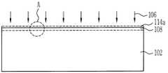
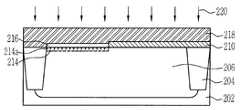
도 3은 도 1c에 도시된 'A' 부위를 확대하여 도시한 도면이다.3 is an enlarged view of a portion 'A' illustrated in FIG. 1C.
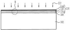
도 4는 도 1e에 도시된 'B' 부위를 확대하여 도시한 도면이다.4 is an enlarged view illustrating a portion 'B' illustrated in FIG. 1E.
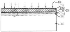
도 5는 도 1f에 도시된 'C' 부위를 확대하여 도시한 도면이다.FIG. 5 is an enlarged view of a portion 'C' shown in FIG. 1F.
도 6a 내지 도 6c는 도 1d 및 도 1e에서 실시되는 산화공정 및 질화공정에 따른 질화층의 프로파일(profile)을 설명하기 위하여 도시한 도면이다.6A to 6C are diagrams for explaining a profile of a nitride layer according to an oxidation process and a nitriding process performed in FIGS. 1D and 1E.
도 7은 본 발명의 실시예에 따른 유전체막의 프로파일을 설명하기 위하여 도시한 도면이다.7 is a diagram illustrating a profile of a dielectric film according to an embodiment of the present invention.
<도면의 주요 부분에 대한 부호의 설명> <Explanation of symbols for the main parts of the drawings>
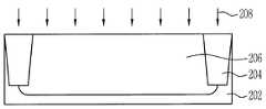
102, 202 : 반도체 기판 104, 208 : 어닐공정 102, 202:
106, 212 : 질소 이온주입공정 106, 212: nitrogen ion implantation process
108, 214 : 질소 주입층 114a 및 114b : 질화층 108, 214:
110 : 산화막 112 : RPN 공정 110: oxide film 112: RPN process
114a, 114b : 질화층 116, 216 : 유전체막 114a and 114b:
118 : 폴리실리콘층 120, 220 : RTP 어닐공정 118:
122, 222 : 캐패시터 122, 222 capacitors
204 : 소자 분리막 206 : 웰 204: device separator 206: well
224 : 트랜지스터 226 : HLD막 224
228 : 소오스 및 드레인 이온주입공정 228 Source and drain ion implantation process
230 : 소오스 및 드레인 접합영역 230 source and drain junction regions
232 : LDD 스페이서 234 : 금속 살리사이드층
232: LDD spacer 234: metal salicide layer
본 발명은 평면 캐패시터 제조방법 및 이를 이용한 반도체 소자의 제조방법에 관한 것으로, 특히 MOS(Metal Oxide Semiconductor)형 캐패시터(capacitor), 즉 평면 캐패시터(planar capacitor)의 제조방법과, 상기 평면 캐패시터와 트랜지스터(또는, 셀)를 포함하는 MPDL(Merged Planar DRAM and Logic) 소자의 제조방법에 관한 것이다.BACKGROUND OF THE
일반적으로, MPDL(Merged Planar DRAM and Logic) 소자에서의 평면 캐패시터의 제조공정을 간략하게 설명하면 다음과 같다. 우선, 소자 분리막이 형성된 p형 반도체 기판에 웰 이온주입(well implant) 공정을 실시하여 캐패시터의 하부전극으로 기능하는 웰(well)을 형성한다. 그런 다음, 순수 산화공정(pure oxidation)을 실시하여 상기 반도체 기판 상에 유전체막(dielectric film)으로 기능하는 게이트 산화막(gate oxide film)을 형성한다. 그런 다음, 전체 구조 상부에 폴리실리콘층(polysilicon layer)을 증착한 후 패터닝하여 캐패시터의 상부전극을 형성한다.In general, the manufacturing process of the planar capacitor in the merged planar DRAM and logic (MPDL) device will be briefly described as follows. First, a well ion implantation process is performed on a p-type semiconductor substrate on which an isolation layer is formed to form a well that functions as a lower electrode of a capacitor. Then, pure oxidation is performed to form a gate oxide film functioning as a dielectric film on the semiconductor substrate. Then, a polysilicon layer is deposited on the entire structure and then patterned to form an upper electrode of the capacitor.
상기에서 설명한 바와 같이 MPDL 소자에서는 산화공정을 실시하여 동일한 두께로 트랜지스터의 게이트 산화막과 캐패시터의 유전체막을 형성한다. 이에 따라, 유전체막의 두께에 많은 제약이 따르게 된다. 최근, MPDL 소자가 점점 고집적화되고, 대용량의 디램(DRAM) 셀(cell)이 요구되면서 정전용량(capacitance)이 큰 유전체막의 필요성이 더욱 커지고 있다. 유전체막의 정전용량을 증가시키기 위해서는 유전체막의 두께(thickness)가 감소되어야 한다. 그러나, 유전체막의 두께를 감소시키는 경우에는 항복전압(breakdown voltage)의 감소, 누설전류(leakage current)의 증가, 동작전류의 감소 및 신뢰성의 감소 등의 문제가 야기된다. 또한, 평면 캐패시터를 이용하여 디램을 구성하는 경우에는 정전용량의 감소에 따라 리프레쉬 타임(refresh time)을 증가시키는데 한계가 있다. 따라서, 디램 신뢰성 향상에도 문제점이 발생할 수 있으며, 이로 인해 MPDL 소자를 비롯한 반도체 소자 제조방법에 많은 제약이 따르게 된다.
As described above, in the MPDL device, an oxidation process is performed to form the gate oxide film of the transistor and the dielectric film of the capacitor with the same thickness. Accordingly, many restrictions are placed on the thickness of the dielectric film. In recent years, as MPDL devices are increasingly integrated and a large capacity DRAM cell is required, the need for a dielectric film having a large capacitance is increasing. In order to increase the capacitance of the dielectric film, the thickness of the dielectric film must be reduced. However, when the thickness of the dielectric film is reduced, problems such as a decrease in breakdown voltage, an increase in leakage current, a decrease in operating current, and a decrease in reliability are caused. In addition, in the case of configuring the DRAM using a planar capacitor, there is a limit to increasing the refresh time according to the reduction of the capacitance. Therefore, problems may also arise in improving the DRAM reliability, which leads to many limitations in the manufacturing method of semiconductor devices including MPDL devices.
따라서, 본 발명은 상기한 종래기술의 문제점을 해결하기 위해 안출된 것으로서, MPDL 소자에서 평면 캐패시터의 유전체막의 두께를 감소시켜 정전용량을 증가시킬 수 있는 평면 캐패시터의 제조방법을 제공하는데 그 목적이 있다.Accordingly, an object of the present invention is to provide a method of manufacturing a planar capacitor which can increase capacitance by reducing the thickness of the dielectric film of the planar capacitor in an MPDL device. .
또한, 본 발명은 평면 캐패시터의 유전체막의 두께를 감소시킴에 따라 야기되는 항복전압의 감소, 누설전류의 증가, 동작전류의 감소 및 신뢰성의 감소 등과 같은 소자의 특성 저하를 해결할 수 있는 평면 캐패시터의 제조방법을 제공하는데 다른 목적이 있다.In addition, the present invention provides a planar capacitor that can solve the deterioration of device characteristics such as a decrease in breakdown voltage, an increase in leakage current, a decrease in operating current, and a decrease in reliability caused by reducing the thickness of the dielectric film of the planar capacitor. There is another purpose in providing a method.
또한, 본 발명은 평면 캐패시터의 유전체막의 두께가 감소된 만큼 GOI(Gate Oxide Integrety) 특성을 향상시킬 수 있는 평면 캐패시터의 제조방법을 제공하는데 또 다른 목적이 있다.In addition, another object of the present invention is to provide a method of manufacturing a planar capacitor capable of improving the gate oxide integrety (GOI) characteristics as the thickness of the dielectric film of the planar capacitor is reduced.
또한, 본 발명은 소자 신뢰성 향상을 위하여 특성이 개선된(advanced) 평면 캐패시터와 트랜지스터를 포함하는 MPDL 소자의 제조방법을 제공하는데 또 다른 목적이 있다.
Another object of the present invention is to provide a method for manufacturing an MPDL device including an advanced planar capacitor and a transistor for improving device reliability.
본 발명의 일측면에 따르면, 웰 이온주입공정을 실시하여 반도체 기판 내에 웰을 형성하는 단계와, 질소 이온주입공정을 실시하여 상기 반도체 기판 내에 질소 주입층을 형성하는 단계와, 산화공정 및 질화공정 또는 상기 질화공정 및 상기 산 화공정을 순차적으로 실시하여 상기 반도체 기판 상에 적어도 하나의 질화층이 포함된 유전체막을 형성하는 단계와, 전체 구조 상부에 폴리실리콘층을 증착하는 단계와, 열처리공정을 실시하여 상기 질소 주입층 내에 존재하는 질소 이온을 외부로 확산시켜 제거함으로써 상기 질소 주입층이 제거되는 단계와, 상기 폴리실리콘층 및 상기 유전체막을 패터닝하는 단계를 포함하는 평면 캐패시터의 제조방법을 제공한다.According to one aspect of the present invention, a well ion implantation process is performed to form a well in a semiconductor substrate, a nitrogen ion implantation process is performed to form a nitrogen injection layer in the semiconductor substrate, an oxidation process and a nitriding process Or sequentially performing the nitriding and oxidizing processes to form a dielectric film including at least one nitride layer on the semiconductor substrate, depositing a polysilicon layer over the entire structure, and performing a heat treatment process. And removing the nitrogen injection layer by diffusing and removing nitrogen ions present in the nitrogen injection layer to the outside, and patterning the polysilicon layer and the dielectric film. .
또한, 본 발명의 다른 측면에 따르면, 캐패시터 영역과 트랜지스터 영역으로 정의되는 반도체 기판을 제공하는 단계와, 웰 이온주입공정을 실시하여 상기 반도체 기판 내에 웰을 형성하는 단계와, 상기 반도체 기판 상에 게이트 산화막용 열산화막을 형성하는 단계와, 상기 캐패시터 영역만 오픈되는 마스크를 이용한 질소 이온주입공정을 실시하여 상기 캐패시터 영역의 상기 반도체 기판의 상부영역에 질소 주입층을 형성하는 단계와, 상기 마스크를 이용한 세정공정을 실시하여 상기 캐패시터 영역의 상기 열산화막을 제거하는 단계와, 상기 마스크를 제거하고, 산화공정 및 질화공정 또는 질화공정 및 산화공정을 순차적으로 실시하여 상기 단계에서 상기 열산화막이 제거된 부위에 적어도 하나의 질화층을 포함하는 캐패시터용 유전체막을 형성하는 단계와, 전체 구조 상부에 폴리실리콘층을 증착하는 단계와, 열처리공정을 실시하여 상기 단계에서 형성된 상기 질소 주입층을 제거하는 단계와, 상기 폴리실리콘층, 상기 유전체막 및 상기 열산화막을 패터닝하여 상기 캐패시터 영역에는 캐패시터를 형성하고, 상기 트랜지스터 영역에는 트랜지스터를 형성하는 단계와, 상기 캐패시터와 상기 트랜지스터 사이에 살리사이드층 형성방지용 절연막을 형성하는 단계와, 소오스 및 드레인 이온주입공정을 실시하여 상기 트랜지스터의 양측의 상기 반도체 기판에 소오스 및 드레인 접합영역을 형성하는 단계와, 전체 구조 상부에 금속층을 증착하고, 열처리공정을 적어도 1회 실시하여 상기 캐패시터, 상기 트랜지스터 및 상기 소오스 및 드레인 접합영역의 상부에 금속 실리사이드층을 형성하는 단계를 포함하는 반도체 소자의 제조방법을 제공한다.In addition, according to another aspect of the invention, providing a semiconductor substrate defined by a capacitor region and a transistor region, performing a well ion implantation process to form a well in the semiconductor substrate, a gate on the semiconductor substrate Forming a nitrogen oxide layer on an upper region of the semiconductor substrate in the capacitor region by forming a thermal oxide layer for an oxide layer, performing a nitrogen ion implantation process using a mask that opens only the capacitor region, and using the mask. Performing a cleaning process to remove the thermal oxide film in the capacitor region, removing the mask, and sequentially performing an oxidation process, a nitriding process, a nitriding process, and an oxidation process to remove the thermal oxide film in the step. Forming a capacitor dielectric film including at least one nitride layer on the substrate Depositing a polysilicon layer over the entire structure, performing a heat treatment process to remove the nitrogen injection layer formed in the step, and patterning the polysilicon layer, the dielectric film, and the thermal oxide film. Forming a capacitor in the capacitor region, forming a transistor in the transistor region, forming an insulating film for preventing the formation of a salicide layer between the capacitor and the transistor, and performing a source and drain ion implantation process to perform the transistor. Forming a source and drain junction region on the semiconductor substrate on both sides of the substrate; depositing a metal layer over the entire structure; and performing a heat treatment process at least once to form the capacitor, the transistor, and the source and drain junction region. Forming a metal silicide layer It provides a method for producing a semiconductor device also.
이하, 첨부된 도면을 참조하여 본 발명의 바람직한 실시예를 설명하기로 한다. 그러나, 본 발명은 이하에서 개시되는 실시예에 한정되는 것이 아니라 서로 다른 다양한 형태로 구현될 수 있으며, 단지 본 실시예는 본 발명의 개시가 완전하도록하며 통상의 지식을 가진자에게 발명의 범주를 완전하게 알려주기 위해 제공되는 것이다.Hereinafter, with reference to the accompanying drawings will be described a preferred embodiment of the present invention. However, the present invention is not limited to the embodiments disclosed below, but may be implemented in various forms, and only the present embodiments are intended to complete the disclosure of the present invention and to those skilled in the art. It is provided for complete information.
도 1a 내지 도 1g는 본 발명의 바람직한 실시예에 따른 평면 캐패시터의 제조방법을 설명하기 위하여 도시한 단면도들이다. 여기서, 도 1a 내지 도 1g에서 도시된 참조부호들 중 서로 동일한 참조부호는 동일한 기능을 하는 동일한 구성요소를 가리킨다.1A to 1G are cross-sectional views illustrating a method of manufacturing a planar capacitor according to an exemplary embodiment of the present invention. Here, the same reference numerals among the reference numerals shown in FIGS. 1A to 1G indicate the same components having the same function.
도 1a를 참조하면, 전처리 세정공정을 통해 상부 표면이 세정된 반도체 기판(102)을 제공한다. 이때, 전처리 세정공정은 DHF(Diluted HF; 50:1의 비율로 H20로 희석된 HF용액)와 SC-1(NH4OH/H2O2/H2O 용액이 소정 비율로 혼합된 용액)을 이용하여 실시하거나, BOE(Buffer Oxide Etchant; 100:1 또는 300:1의 비율로 H2O로 희석된 HF와 NH4F의 혼합용액[1:4 내지 1:7])와 SC-1을 이용하여 실시하는 것이 바 람직하다.Referring to FIG. 1A, a
한편, 반도체 기판(102)에는 반도체 기판(102)을 활성영역과 필드영역으로 정의하기 위한 소자 분리막(도시하지 않음)이 형성될 수 있다. 이 경우, 소자 분리막은 STI(Shallow Trench Isolation) 스킴(scheme)을 이용하여 형성하거나, LOCOS(LOCal Oxidation of silicon) 스킴(scheme)을 이용하여 형성한다. 소자 분리막은 고집적화를 구현하기 위하여 LOCOS 스킴 대신에 STI 스킴을 이용하여 형성하는 것이 바람직하다.Meanwhile, an isolation layer (not shown) may be formed in the
이어서, 반도체 기판(102)에 대하여 웰 이온주입(well implant)공정을 실시하여 반도체 기판(102) 내에 웰(도시하지 않음)을 형성한다. 웰은 구현하고자 하는 소자의 물성 특성에 따라 p-웰 또는 n-웰로 형성된다. p-웰은 'p-' 불순물인 보론(boron)을 주입하여 형성한다. n-웰은 'n-' 불순물인 인(phosphorous)을 주입하여 형성한다.Subsequently, a well ion implantation process is performed on the
도 1b를 참조하면, 웰에 대하여 어닐(anneal)공정(104)을 실시한다. 이와 같이, 어닐공정(104)을 실시하는 이유는 캐패시터의 정전용량을 증가시키기 위함이다. 어닐공정(104)을 실시하는 경우 웰에 주입된 불순물의 농도가 높아지며, 이에 따라 정전용량도 증가하게 된다.Referring to FIG. 1B, an
어닐공정(104)을 실시하여 웰 내의 도핑농도를 증가시키면, 후속 캐패시터 유전체막의 일렉트릭컬(electrical) 두께가 감소하게 되는 효과가 있으며, 이를 일렉트리컬 산화막으로 환산하면 2 내지 3Å의 두께가 감소하는 효과가 발생하게 된 다. 다시 말하면, 불순물의 농도가 높아지면 단위면적당 Rs(Sheet Resistance)는 작아지게 되고, 캐리어(carrier)의 이동도(density)가 크게 된다. 따라서, 불순물 농도가 높아져 축적용량(accumulation capacitance)이 증가되는 정도는 실제 캐패시터 유전체막의 두께가 감소되어 정전용량이 증가되는 정도와 거의 유사하다. 이 것을 일렉트리컬 산화막 두께로 환산하면 2 내지 3Å 정도가 된다. 따라서, 본 발명의 바람직한 실시예에서는 일렉트리컬 산화막의 두께가 2 내지 3Å 정도의 두께가 되도록 불순물 농도를 증가시킨다.Increasing the doping concentration in the well by performing the
예컨대, 어닐공정(104)은 퍼니스(furnace)를 이용하여 다음과 같은 단계로 이루어진다. 먼저, 반도체 기판(102)을 퍼니스 내부로 로딩(loading) 시킨다. 그런 다음, 상기 퍼니스 내부로 질소(N2) 가스를 유입시켜 질소 분위기(N2 ambient)를 형성한다. 그런 다음, 상기 퍼니스 내부를 850℃(±100℃) 온도 범위로 유지시킨 상태에서 10분(±2분) 동안 유지한다. 그런 다음, 반도체 기판(102)을 상기 퍼니스 외부로 언로딩(unloading)시켜 공정을 마무리 한다.For example, the
상기에서 설명한 어닐공정(104) 단계는 이해의 편의를 위해 일례로 설명하였을 뿐 이에 한정되는 것이 아니다. 즉, 어닐공정(104) 단계는 서로 바뀔 수 있다. 한편, 어닐공정(104)은 거의 100% 질소 분위기에서 850℃의 온도로 10분 동안 실시하는 것이 바람직하다. 여기서, 어닐공정(104)을 거의 100%의 질소 분위기에서 실시하는 이유는 산소(O2)가 유입되는 경우, 산소에 의해 반도체 기판(102) 상부 표면에 소정의 산화막이 형성되기 때문이다.The
도 1c를 참조하면, 질소 이온주입(nitrogen implant)공정(106)을 실시한다. 이로써, 도 3에 도시된 바와 같이 반도체 기판(102)의 상부 영역에는 다량의 질소(108a)가 주입되어 질소 주입층(108)이 형성된다. 이와 같이, 질소 이온주입공정(106)을 실시하는 이유는 캐패시터의 유전체막의 두께를 감소시키기 위함이다. 즉, 반도체 기판(102) 내에 질소 주입층(114)을 형성함으로써 후속 캐패시터의 유전체막을 형성하기 위하여 도 1d에서 실시되는 열산화(thermal oxidation)공정시 형성되는 산화막(110)의 두께를 제어할 수 있다.Referring to FIG. 1C, a nitrogen
예컨대, 질소 이온주입공정(106)은 질소 이온(원자량; 14)을 이용하여 2e14atoms/cm2(±0.5e14atoms/cm2)의 도즈(dose), 10KeV(±1KeV)의 이온주입에너지로 실시한다. 바람직하게는, 질소 이온을 이용하여 2e14atoms/cm2의 도즈, 10KeV의 이온주입에너지로 실시한다.For example, the nitrogen
한편, 질소 이온주입공정(106)시 반도체 기판(102)의 상부 표면이 손상을 입게 되는 경우가 발생된다. 이러한 반도체 기판(102)의 상부 표면의 손상을 방지하기 위하여 질소 이온주입공정(106) 전에 반도체 기판(102) 상에 질소 이온주입공정(106)의 버퍼층(buffer layer) 또는 베리어층(barrier layer)으로 열산화막(thermal oxide; 도시하지 않음)을 형성할 수 있다. 이 경우, 열산화막은 50Å(±10Å)으로 형성한다. 바람직하게는 50Å으로 형성한다.On the other hand, during the nitrogen
상기에서 질소 이온주입공정(106)을 실시하기 전에 반도체 기판(102) 상에 열산화막을 형성하는 경우, 도 3에 도시된 바와 같이 질소 이온주입공정(106)에 의 해 열산화막과 반도체 기판(102)의 계면(interface)에 질화층(114a)이 아주 미미하게 형성된다.In the case where the thermal oxide film is formed on the
도 1d를 참조하면, 도 1c에서 열산화막을 형성하는 경우에는 세정공정을 실시하여 상기 열산화막을 제거한다. 이때, 세정공정은 BOE(Buffer Oxide Etchant; 100:1 또는 300:1의 비율로 H2O로 희석된 HF와 NH4F의 혼합용액[1:4 내지 1:7])를 이용하여 실시한다.Referring to FIG. 1D, when the thermal oxide film is formed in FIG. 1C, a cleaning process is performed to remove the thermal oxide film. At this time, the washing process is performed using BOE (Buffer Oxide Etchant; mixed solution of HF and NH4 F diluted with H2 O at a ratio of 100: 1 or 300: 1 [1: 4 to 1: 7]). .
이어서, 전체 구조 상부에 대하여 열 산화공정(thermal oxidation) 또는 ISSG(In-Situ Steam Generation-wet)을 실시한다. 이로써, 반도체 기판(102) 상에 캐패시터 유전체막용 산화막(SiO2, 110)이 형성된다. 이때, 열 산화공정은 습식(wet) 또는 건식(dry) 산화공정으로 실시한다. 습식 산화공정은 습식 H2/O2 분위기에서 700 내지 900℃로 40 내지 60초 동안 실시한다. 바람직하게는 습식 H2/O2 분위기에서 800℃로 50초 동안 실시한다.Subsequently, thermal oxidation or In-Situ Steam Generation-wet (ISSG) is performed on the entire structure. As a result, oxide films (SiO2 , 110) for a capacitor dielectric film are formed on the
도 1e를 참조하면, 도 1d에서 실시되는 열 산화공정과 인시튜(in-situ)로 질화공정(112)을 실시한다. 질화공정(112)은 NO, N20, NH3, RPN(Remote Plasma Nitridation) 또는 DPN(Decoupled Plasma Nitridation)으로 실시한다. 이로써, 도 4에 도시된 바와 같이, 산화막(110)의 상부영역에 질화층(114b)이 형성된다. 여기서, 질화층(114b)은 산화막(110)의 상부에 형성되는 것으로 도시되어 있으나, 실제로는 질화층(114)의 상부가 산화막(110) 두께의 80 내지 90% 지점에 위치된다. 또 한, 질화층(114b)은 산화막(110) 전체 두께의 1/3 정도의 두께로 형성하는 것이 바람직하다. 이로써, 질화층(114a), 산화막(110) 및 질화층(114b)으로 이루어진 유전체막(116)이 형성된다.Referring to FIG. 1E, the
일례로, RPN 공정은 상기 산화공정이 실시되는 동일 챔버(chamber) 내에서 다음과 같은 단계로 이루어진다. 먼저, 산화공정이 완료된 후 챔버 내부로 질소(N2) 가스를 유입시켜 질소 분위기(N2 ambient)를 형성한다. 그런 다음, 상기 챔버 내부를 400℃(±100℃) 온도 범위로 유지시킨 상태에서 10분(±2분) 동안 유지한다. 그런 다음, 반도체 기판(102)을 상기 챔버 외부로 언로딩시켜 공정을 마무리 한다. 여기서, RPN 공정단계는 이해의 편의를 위해 일례로 설명하였을 뿐 이에 한정되는 것이 아니다. 즉, RPN 공정단계는 서로 바뀔 수 있다. 한편, RPN 공정은 질소 분위기에서 400℃의 온도로 10분 동안 실시하는 것이 바람직하다.In one example, the RPN process consists of the following steps in the same chamber in which the oxidation process is carried out. First, after the oxidation process is completed, nitrogen (N2 ) gas is introduced into the chamber to form a nitrogen atmosphere (N2 ambient). Then, the inside of the chamber is maintained for 10 minutes (± 2 minutes) while maintaining the temperature in the 400 ℃ (± 100 ℃) range. Then, the
한편, 본 발명의 바람직한 실시예에 따른 캐패시터 제조방법은 도 1d 및 도 1e에서 설명한 내용에 한정되는 것이 아니다. 예컨대, 도 1d에서 실시되는 열 산화공정 전에 먼저 도 1e에서 실시되는 질화공정(112), 예컨대 NO 어닐공정을 실시하여 질화층을 형성한 후 후속으로 재산화(reoxidation) 공정을 실시하여 산화막을 형성할 수도 있다. 이 경우에는 반도체 기판(102) 상부에 질화층이 먼저 형성되고, 후속 재산화공정에 의해 질화층과 반도체 기판(102) 사이에 산화막이 성장되게 된다.Meanwhile, the capacitor manufacturing method according to the preferred embodiment of the present invention is not limited to the contents described with reference to FIGS. 1D and 1E. For example, prior to the thermal oxidation process performed in FIG. 1D, a
상기 도 1d 및 도 1e에서 실시되는 산화공정 및 질화공정(112)에 따라 변화 되는 질화층의 농도(concentration) 및 깊이(depth)를 도 6a 내지 도 6c를 통해 설명하기로 한다.Concentration and depth of the nitride layer changed according to the oxidation process and the
도 6a는 먼저 열 산화공정을 실시한 후 인-시튜로 NO 어닐공정을 실시하는 경우 질화층(114b)의 프로파일(profile)을 도시한 도면이다. 이 경우에는 도 6a에 도시된 바와 같이, 열 산화공정에 의해 반도체 기판(Si) 상에 산화막(SiO2)이 먼저 형성된 후, NO 어닐공정에 의해 산화막(SiO2)과 반도체 기판(Si)의 계면 사이에 질화층(114b)이 형성된다.FIG. 6A is a diagram illustrating a profile of the
도 6b는 먼저 NO 어닐공정을 실시한 후 재산화공정을 실시하는 경우 질화층(114b)의 프로파일을 도시한 도면이다. 이 경우에는 도 6b에 도시된 바와 같이, NO 어닐공정에 의해 반도체 기판(Si) 상에 질화층(114b)이 먼저 형성된 후, 재산화공정에 의해 질화층(114b)과 반도체 기판(Si) 사이에 산화막(SiO2)이 성장되어 형성된다.FIG. 6B shows a profile of the
도 6c는 먼저 열산화공정을 실시한 후 플라즈마 질화(plasma nitridation)공정을 실시하는 경우 질화층(114b)의 프로파일을 도시한 도면이다. 이 경우에는 도 6c에 도시된 바와 같이, 열 산화공정에 의해 반도체 기판(Si) 상에 산화막(SiO2)이 먼저 형성된 후, 플라즈마 질화공정에 의해 산화막(SiO2)과 반도체 기판(Si)의 계면 사이에 질화층(114b)이 형성된다.FIG. 6C illustrates a profile of the
상기에서 설명한 공정들을 실시함으로써 도 7과 같은 프로파일을 갖는 유전 체막(116)이 형성된다. 즉, 유전체막(116)은 질화층(114a), 산화막(110) 및 질화층(114b)으로 이루어진다. 이로써, PMOS의 경우에는 보론 침투(boron penetration)를 방지할 수 있다. 또한, 핫 전자(resist hot electron)의 감소에 따른 영향도 최소화할 수 있다.By performing the processes described above, the
도 1f를 참조하면, 전체 구조 상부에 캐패시터의 상부전극용으로 폴리실리콘층(118)을 형성한다. 이때, 폴리실리콘층(118)은 LPCVD(Low Pressure Chemical Vapor Deposition) 공정으로 도프트(doped) 비정질 실리콘막으로 형성하거나, 언도프트(undoped) 비정질 실리콘막으로 형성할 수 있다. 예컨대, 도프트 비정질 실리콘막은 SiH4 또는 Si2H6와 PH3 가스를 이용하여 형성한다. 언도프트 비정질 실리콘막은 SiH4 또는 Si2H6가스를 이용하여 형성한다.Referring to FIG. 1F, a
이어서, 전체 구조 상부에 대하여 열처리공정(120)을 실시한다. 예컨대, 열처리공정(120)은 RTP(Rapid Temperature Process) 어닐공정으로 실시한다. 이러한 RTP 어닐공정은 도 5에 도시된 바와 같이 반도체 기판(102)의 상부 영역에 형성된 질소 주입층(108)에 존재하는 질소원자(108a)를 외부로 확산(out diffusion)시켜 제거하는 역할을 한다. 반도체 기판(102)의 상부 영역에 존재하는 질소 주입층(108)을 제거시킴으로써 누설전류를 감소시키게 된다. 이에 따라 유전체막(116)의 신뢰성 및 GOI 특성을 향상시킬 수 있다.Subsequently, the
예컨대, RTP 어닐공정 단계를 설명하면 다음과 같다. RTP 어닐공정은 은 반도체 기판(102)을 챔버 내부로 로딩시킨 후, 상기 챔버 내부로 질소(N2) 가스를 유 입시켜 질소 분위기(N2 ambient)를 형성한다. 그런 다음, 상기 챔버 내부를 900℃(±100℃) 온도 범위로 유지시킨 상태에서 10초(±1초) 동안 유지한다. 그런 다음, 반도체 기판(102)을 상기 챔버 외부로 언로딩시켜 공정을 마무리 한다. 한편, RTP 어닐공정(120)은 질소 분위기에서 900℃의 온도로 10초 동안 실시하는 것이 바람직하다.For example, the RTP annealing process step will be described below. In the RTP annealing process, the
도 1g를 참조하면, 포토리소그래피(photolithography) 공정 및 식각공정을 실시하여 상부전극용 폴리실리콘층(118) 및 유전체막(116)을 원하는 형태로 패터닝한다. 이로써, 캐패시터(122)가 완성된다.Referring to FIG. 1G, a photolithography process and an etching process are performed to pattern the upper
이하에서는, 도 1a 내지 도 1g를 통해 설명한 캐패시터 제조방법을 이용한 MPDL 소자의 제조방법을 도 2a 내지 도 2h를 통해 설명하기로 한다. 여기서, 도 2a 내지 도 2h에서 도시된 참조부호들 중 서로 동일한 참조부호는 동일한 기능을 하는 동일한 구성요소를 가리킨다.Hereinafter, a method of manufacturing an MPDL device using the capacitor manufacturing method described with reference to FIGS. 1A to 1G will be described with reference to FIGS. 2A to 2H. Here, the same reference numerals among the reference numerals shown in FIGS. 2A to 2H indicate the same components having the same function.
도 2a를 참조하면, 캐패시터가 형성될 영역(이하, '캐패시터 영역'이라 함)(CR; Capacitor Region)과, 트랜지스터가 형성될 영역(이하, '트랜지스터 영역'이라 함)(TR; Transistor Region)으로 정의된(defined) 반도체 기판(202)을 제공한다.Referring to FIG. 2A, a region where a capacitor is to be formed (hereinafter referred to as a 'capacitor region') (CR) and a region where a transistor is to be formed (hereinafter referred to as a 'transistor region') (TR) A
반도체 기판(202)에는 반도체 기판(202)을 활성영역과 필드영역으로 정의하기 위한 소자 분리막(204)이 형성된다. 소자 분리막(204)은 STI 스킴을 이용하여 형성한다.In the
이어서, 반도체 기판(202)에 대하여 웰 이온주입공정을 실시하여 반도체 기판(202) 내에 웰(206)을 형성한다. 웰(206)은 구현하고자 하는 소자의 물성 특성에 따라 p-웰 또는 n-웰로 형성된다. p-웰은 'p-' 불순물인 보론을 주입하여 형성한다. n-웰은 'n-' 불순물인 인을 주입하여 형성한다.Subsequently, a well ion implantation process is performed on the
도 2b를 참조하면, 웰(206)에 대하여 어닐공정(208)을 실시한다. 도 1b에서 설명한 바와 같이 어닐공정(208)을 실시하는 이유는 캐패시터의 정전용량을 증가시키기 위함이다. 이때, 어닐공정(208)은 도 1b에서 실시된 어닐공정(104)과 동일한 방법으로 실시한다.Referring to FIG. 2B, an
도 2c를 참조하면, 전체 구조 상부에 게이트 산화막용 열산화막(210)을 형성한다. 열산화막(210)은 캐패시터 영역(CR)에서 버퍼층 또는 후속 질소 이온주입공정(212)시 베리어층으로 기능한다. 트랜지스터 영역(TR)에서는 게이트 산화막으로 기능한다. 열산화막(210)은 50Å(±10Å)으로 형성한다. 바람직하게는 50Å으로 형성한다.Referring to FIG. 2C, a
이어서, 전체 구조 상부에 포토레지스트(photoresist; 미도시)를 도포한 후, 포토 마스크(photo mask)를 이용한 노광공정 및 현상공정을 순차적으로 실시하여 포토레지스트 패턴(PR)을 형성한다. 이때, 포토레지스트 패턴(PR)은 캐패시터 영역(CR)만 오픈(open)되도록 형성한다.Subsequently, a photoresist (not shown) is applied over the entire structure, and then an exposure process and a development process using a photo mask are sequentially performed to form a photoresist pattern PR. In this case, the photoresist pattern PR is formed so that only the capacitor region CR is opened.
이어서, 포토레지스트 패턴(PR)을 마스크로 이용하여 질소 이온주입공정(212)을 실시한다. 이로써, 캐패시터 영역(CR)의 반도체 기판(202)에 는 다량의 질소가 주입되어 질소 주입층(214)이 형성된다. 질소 이온주입공정(212)은 질소 이온을 이용하여 2e14atoms/cm2(±0.5e14atoms/cm2)의 도즈, 10KeV(±1KeV)의 이온주입에너지로 실시한다. 바람직하게는 질소 이온을 이용하여 2e14atoms/cm2의 도즈, 10KeV의 이온주입에너지로 실시한다. 이때, 질소 이온주입공정(212)에 의해 반도체 기판(202)와 열산화막(210) 사이의 계면에는 질화층(도시하지 않음)이 미미하게 나마 형성된다.Next, the nitrogen
도 2d를 참조하면, 포토레지스트 패턴(PR)을 그대로 식각 마스크로 이용한 세정공정을 실시하여 캐패시터 영역(CR)의 열산화막(210)을 제거한다. 이때, 세정공정은 BOE(Buffer Oxide Etchant; 100:1 또는 300:1의 비율로 H2O로 희석된 HF와 NH4F의 혼합용액[1:4 내지 1:7])를 이용하여 실시한다.Referring to FIG. 2D, the
이어서, 포토레지스트 패턴(PR)을 스트립(strip) 공정을 실시하여 제거한다. 그런 다음, 열 산화공정과 질화공정을 인시튜로 실시하여 열산화막(210)이 제거된 부위에 열산화막(210)보다 얇게 산화막(도시하지 않음)과 질화층(도시하지 않음)을 형성한다. 이로써, 도 2c에서 실시되는 질소 이온주입공정(212)에 의해 형성된 질화층과, 열산화공정 및 질화공정으로 형성된 산화막 및 질화층으로 이루어진 유전체막(216)이 형성된다. 여기서, 상기 열 산화공정과 상기 질화공정은 도 1d 및 도 1e에서 실시되는 방법과 동일한 방법으로 실시된다.Subsequently, the photoresist pattern PR is removed by performing a strip process. Then, the thermal oxidation process and the nitriding process are performed in situ to form an oxide film (not shown) and a nitride layer (not shown) in a portion thinner than the
이어서, 전체 구조 상부에 폴리실리콘층(218)을 증착한다. 이때, 폴리실리콘 층(218)은 LPCVD 공정으로 도프트 비정질 실리콘막으로 증착하거나, 언도프트 비정질 실리콘막으로 증착할 수 있다. 예컨대, 도프트 비정질 실리콘막은 SiH4 또는 Si2H6와 PH3 가스를 이용하여 증착한다. 언도프트 비정질 실리콘막은 SiH4 또는 Si2H6가스를 이용하여 증착한다.Next, a
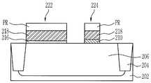
도 2e를 참조하면, 전체 구조 상부에 대하여 열처리공정(220)을 실시한다. 예컨대, 열처리공정(220)은 RTP 어닐공정으로 실시한다. 이러한 RTP 어닐공정은 질화층(214)에 존재하는 질소원자(214a)를 외부로 확산시켜 제거하는 기능을 한다. 반도체 기판(202) 내에 질소 이온주입공정(212)에 의해 형성된 질소 주입층(214)을 제거시킴으로써 누설전류를 감소시킬 수 있다. 다시 말하면, 질소 이온주입공정(212)에 의해 형성된 질소 주입층(214)은 기판내 결점(defect)으로 작용하여 누설전류를 증가시키게 된다. 따라서, 질소 주입층(214)을 제거시킴으로써 누설전류를 감소시킬 수 있는 것이다. 예컨대, RTP 어닐공정은 질소 분위기에서 900℃(±100℃) 온도 범위로 10초(±1초) 동안 실시한다. 바람직하게는 질소 분위기에서 900℃의 온도로 10초 동안 실시한다.Referring to FIG. 2E, a
도 2f를 참조하면, 전체 구조 상부에 포토레지스트를 도포한 후 포토 마스크를 이용한 노광공정 및 현상공정을 순차적으로 실시하여 포토레지스트 패턴(PR)을 형성한다. 그런 다음, 상기 포토리소그래피 패턴(PR)을 이용한 식각공정을 실시한다. 이로써, 캐패시터 영역(CR)에는 폴리실리콘층(218) 및 유전체막(216)이 패터닝되어 캐패시터(222)가 형성된다. 트랜지스터 영역(TR)에는 폴리실리콘층(218) 및 열산화막(210)이 패터닝되어 트랜지스터(224)가 형성된다. 그런 다음, 상기 포토레지스트 패턴(PR)은 스트립 공정에 의해 제거된다.Referring to FIG. 2F, after the photoresist is applied over the entire structure, an exposure process and a development process using a photo mask are sequentially performed to form a photoresist pattern PR. Then, an etching process using the photolithography pattern PR is performed. As a result, the
도 2g를 참조하면, 전체 구조 상부에 HLD(High temperature Low pressure Dielectric)막을 증착한다. 그런 다음, HLD막에 대하여 HF 세정(HF cleaning)을 이용하여 벌크 에치(bulk etch)를 실시한다. 상기 벌크 에치는 마스크 공정없이 에치백(etch back) 하는 공정을 말하며, 후속 공정을 통해 도시되지 않은 넌 살리사이드 영역(non-salicide region)에 대한 마스크 작업을 실시한 후 HF 세정으로 스페이서 부분을 제거하게 된다. 이러한 과정을 거치면, 캐패시터(222)와 트랜지스터(224) 사이에만 HLD막이 잔류된다. 상기 잔류되는 HLD막(226)은 이 부위에서 살리사이드(SALICIDE)가 형성되지 않도록 하는 살리사이드 블럭킹(blocking) 기능을 한다.Referring to FIG. 2G, a high temperature low pressure dielectric (HLD) film is deposited on the entire structure. Then, bulk etch is performed on the HLD film using HF cleaning. The bulk etch refers to a process of etching back without a mask process, and performing a mask operation on a non-salicide region (not shown) through a subsequent process to remove the spacer portion by HF cleaning. do. Through this process, the HLD film remains only between the
이어서, 전체 구조 상부에 대하여 소오스 및 드레인 이온주입공정(228)을 실시한다. 이로써, 트랜지스터(224)의 양측의 반도체 기판(202)에는 소오스 및 드레인 접합영역(230)이 형성된다. 한편, 소오스 및 드레인 이온주입공정(228)은 트랜지스터(224)의 물성적 특성에 따라 다르게 진행된다. 예컨대, 트랜지스터(224)가 NMOS 경우에는 비소(As) 이온을 1E15 내지 1E16atoms/cm2의 도즈량으로 하여 10 내지 40KeV의 이온주입에너지로 실시할 수 있다. PMOS 경우에는 붕소(B) 이온을 1E15 내지 1E16atoms/cm2의 도즈량으로 하여 1 내지 10KeV의 이온주입에너지로 실시할 수 있다.Subsequently, the source and drain
도 2h를 참조하면, 전체 구조 상부에 HLD막(도시하지 않음)을 증착한다. 그런 다음, 블랭켓 에치(blanket etch) 또는 에치백(etch back) 방식과 같은 직진성 건식(dry) 식각공정으로 상기 HLD막을 식각한다. 이로써, 트랜지스터(224)의 측벽에는 LDD(Lightly Doped Drain) 스페이서(spacer)(232)가 형성된다. 여기서, 트랜지스터(224)의 측벽에 LDD 스페이서(232)를 형성하는 이유는 후속 살리사이드 형성공정시 살리사이드층이 트랜지스터(224)의 측벽에 형성되는 것을 방지하기 위함이다.Referring to FIG. 2H, an HLD film (not shown) is deposited on the entire structure. Then, the HLD film is etched by a straight dry etching process such as a blanket etch or an etch back method. As a result, a lightly doped drain (LDD) spacer 232 is formed on the sidewall of the
이어서, 전체 구조 상부에 니켈(nickel), 티타늄(Titanium; Ti) 및 코발트(Cobalt; Co) 등을 이용하여 금속층(도시하지 않음)을 증착한다. 예컨대, 금속층은 접합누설전류를 고려하여 70Å(±20Å)의 두께로 형성하는 것이 바람직하다. 그런 다음, 상기 금속층을 보호하기 위하여 캡핑층(도시하지 않음)을 형성할 수도 있다. 이때, 상기 캡핑층으로는 코발트, 니켈, 티타늄 또는 티타늄 질화막으로 형성할 수 있다. 그런 다음, 전체 구조 상부에 RTP 방식으로 열처리공정을 적어도 1회 이상 실시하여 캐패시터(222), 트랜지스터(224) 및 노출되는 소오스 및 드레인 접합영역(230) 상에 금속 살리사이드층(234)을 형성한다. 이때, 상기 열처리공정은 400 내지 500℃의 온도범위에서 실시한다. 그런 다음, H2SO4와 H2O2를 소정 비율로 혼합한 혼합용액을 이용한 세정공정을 실시하여 반응하지 않고 미반응된 금속을 제거한다.Subsequently, a metal layer (not shown) is deposited on the entire structure using nickel, titanium (Ti), cobalt (Co), or the like. For example, the metal layer is preferably formed to a thickness of 70 mA (± 20 mA) in consideration of the junction leakage current. Then, a capping layer (not shown) may be formed to protect the metal layer. In this case, the capping layer may be formed of cobalt, nickel, titanium, or titanium nitride. Then, the
상기에서 설명한 본 발명의 기술적 사상은 바람직한 실시예에서 구체적으로 기술되었으나, 상기한 실시예는 그 설명을 위한 것이며, 그 제한을 위한 것이 아님을 주의하여야 한다. 또한, 본 발명은 본 발명의 기술 분야의 통상의 전문가라면 본 발명의 기술적 사상의 범위 내에서 다양한 실시예가 가능함을 이해할 수 있을 것이다.
Although the technical spirit of the present invention described above has been described in detail in a preferred embodiment, it should be noted that the above embodiment is for the purpose of description and not of limitation. In addition, the present invention will be understood by those skilled in the art that various embodiments are possible within the scope of the technical idea of the present invention.
이상에서 설명한 바와 같이, 본 발명에서는 웰 형성 후 어닐공정을 실시하여 웰에 주입된 이온의 농도을 증가시킴으로써 캐패시터의 정전용량을 증가시킬 수 있다.As described above, in the present invention, the capacitance of the capacitor may be increased by performing an annealing process after the well formation to increase the concentration of ions injected into the well.
또한, 본 발명에서는 캐패시터의 유전체막을 형성하기 전에, 질소 이온주입공정을 실시하여 웰(즉, 반도체 기판)의 상부영역에 질소가 다량 주입된 질소 주입층이 존재되도록 함으로써 후속 산화공정에 의해 형성되는 유전체막의 두께를 감소시키는 것이 가능하다.In addition, in the present invention, before forming the dielectric film of the capacitor, a nitrogen ion implantation process is performed to allow a nitrogen injection layer in which a large amount of nitrogen is injected into the upper region of the well (ie, the semiconductor substrate) to be formed by a subsequent oxidation process. It is possible to reduce the thickness of the dielectric film.
또한, 본 발명에서는 산화공정을 실시하여 산화막을 형성한 후 인시튜 방식으로 RPN 공정을 실시하여 상기 산화막의 상하부에 질화층을 형성하고, 이 들을 유전체막으로 사용함으로써 PMOS 트랜지스터의 경우 보론 침투에 의한 소자 특성의 저하를 방지할 수 있다.In addition, in the present invention, after forming an oxide film by performing an oxidation process, a RPN process is performed in situ to form a nitride layer on the upper and lower portions of the oxide film, and these are used as dielectric films. The fall of an element characteristic can be prevented.
또한, 본 발명에서는 RTP 방식으로 열처리공정을 실시하여 질소 이온주입공정으로 형성된 질화층을 제거하고, 이에 따라 이 부위에서의 누설전류를 감소시켜 캐패시터의 유전체막의 신뢰성 및 GOI 특성을 향상시킬 수 있다. 또한, 캐패시터의 정전용량을 50% 이상 증가시킬 수 있다.In addition, in the present invention, by performing a heat treatment process by the RTP method to remove the nitride layer formed by the nitrogen ion implantation process, it is possible to improve the reliability and GOI characteristics of the dielectric film of the capacitor by reducing the leakage current at this site. In addition, the capacitance of the capacitor can be increased by 50% or more.
결국, 본 발명은 캐패시터의 유전체막의 두께를 감소시켜 캐패시터의 정전용량을 증가시키는 한편, 상기 유전체막의 감소에 따라 야기되는 문턱전압의 감소, 누설전류의 증가, 동작 전류의 감소, 유전체막의 신뢰성 감소 및 GOI 특성 저하 등을 해결할 수 있다. 따라서, 본 발명은 향후 반도체 기술이 고집적화되어 소자 분리막의 간격이 줄어들지라도 크게 영향을 미치지 않으며, MPDL에서 구현하는 캐패시터의 셀 크기 또한 캐패시터의 정전용량이 증가하는 정도만큼 작게 할 수 있다는 장점이 있다.
As a result, the present invention reduces the thickness of the dielectric film of the capacitor to increase the capacitance of the capacitor, while reducing the threshold voltage caused by the decrease of the dielectric film, increasing the leakage current, reducing the operating current, decreasing the reliability of the dielectric film, and Deterioration of GOI characteristics can be solved. Therefore, the present invention does not significantly affect the semiconductor technology due to the high integration of the device isolation layer, and the cell size of the capacitor implemented in the MPDL can be reduced as much as the capacitance of the capacitor increases.
Claims (24)
Translated fromKoreanPriority Applications (1)
| Application Number | Priority Date | Filing Date | Title |
|---|---|---|---|
| KR1020030008122AKR100952578B1 (en) | 2003-02-10 | 2003-02-10 | Manufacturing method of planar capacitor and manufacturing method of semiconductor device using same |
Applications Claiming Priority (1)
| Application Number | Priority Date | Filing Date | Title |
|---|---|---|---|
| KR1020030008122AKR100952578B1 (en) | 2003-02-10 | 2003-02-10 | Manufacturing method of planar capacitor and manufacturing method of semiconductor device using same |
Publications (2)
| Publication Number | Publication Date |
|---|---|
| KR20040072156A KR20040072156A (en) | 2004-08-18 |
| KR100952578B1true KR100952578B1 (en) | 2010-04-12 |
Family
ID=37359754
Family Applications (1)
| Application Number | Title | Priority Date | Filing Date |
|---|---|---|---|
| KR1020030008122AExpired - Fee RelatedKR100952578B1 (en) | 2003-02-10 | 2003-02-10 | Manufacturing method of planar capacitor and manufacturing method of semiconductor device using same |
Country Status (1)
| Country | Link |
|---|---|
| KR (1) | KR100952578B1 (en) |
Cited By (1)
| Publication number | Priority date | Publication date | Assignee | Title |
|---|---|---|---|---|
| KR20230027489A (en) | 2021-08-19 | 2023-02-28 | 주식회사 키파운드리 | Single poly non-volatile memory device and manufacturing method thereof |
Citations (4)
| Publication number | Priority date | Publication date | Assignee | Title |
|---|---|---|---|---|
| KR950012704A (en)* | 1993-10-12 | 1995-05-16 | 김주용 | Capacitor Manufacturing Method of Semiconductor Device |
| KR20000045274A (en)* | 1998-12-30 | 2000-07-15 | 김영환 | Fabrication method of capacitor |
| KR20000065605A (en)* | 1999-04-07 | 2000-11-15 | 윤종용 | Method for Forming a Capacitor Using Oxygen Ion Implantation, a Semiconductor Device Having Oxygen Ion Implanted Platinum Family Metal Layer and Manufacturing Method Thereof |
| KR20020002639A (en)* | 2000-06-30 | 2002-01-10 | 박종섭 | A method for forming a storage node of a semiconductor device |
- 2003
- 2003-02-10KRKR1020030008122Apatent/KR100952578B1/ennot_activeExpired - Fee Related
Patent Citations (4)
| Publication number | Priority date | Publication date | Assignee | Title |
|---|---|---|---|---|
| KR950012704A (en)* | 1993-10-12 | 1995-05-16 | 김주용 | Capacitor Manufacturing Method of Semiconductor Device |
| KR20000045274A (en)* | 1998-12-30 | 2000-07-15 | 김영환 | Fabrication method of capacitor |
| KR20000065605A (en)* | 1999-04-07 | 2000-11-15 | 윤종용 | Method for Forming a Capacitor Using Oxygen Ion Implantation, a Semiconductor Device Having Oxygen Ion Implanted Platinum Family Metal Layer and Manufacturing Method Thereof |
| KR20020002639A (en)* | 2000-06-30 | 2002-01-10 | 박종섭 | A method for forming a storage node of a semiconductor device |
Cited By (2)
| Publication number | Priority date | Publication date | Assignee | Title |
|---|---|---|---|---|
| KR20230027489A (en) | 2021-08-19 | 2023-02-28 | 주식회사 키파운드리 | Single poly non-volatile memory device and manufacturing method thereof |
| US11825650B2 (en) | 2021-08-19 | 2023-11-21 | Key Foundry Co., Ltd. | Single poly non-volatile memory device and manufacturing method thereof |
Also Published As
| Publication number | Publication date |
|---|---|
| KR20040072156A (en) | 2004-08-18 |
Similar Documents
| Publication | Publication Date | Title |
|---|---|---|
| KR100568859B1 (en) | Method for manufacturing transistor of DRAM semiconductor device | |
| JP2004095918A (en) | Semiconductor storage device and method of manufacturing semiconductor device | |
| TW495967B (en) | Semiconductor integrated circuit device and the manufacturing method thereof | |
| JP2000332237A (en) | Method for manufacturing semiconductor device | |
| CN101770989B (en) | Formation method of semiconductor structure | |
| US20020102796A1 (en) | Method for forming dual gate electrode for semiconductor device | |
| JP2802263B2 (en) | Method for manufacturing semiconductor device | |
| JP2005340329A (en) | Semiconductor device and manufacturing method thereof | |
| US20020168828A1 (en) | Method of reducing threshold voltage shifting of a gate | |
| US5882962A (en) | Method of fabricating MOS transistor having a P+ -polysilicon gate | |
| US6124187A (en) | Method of fabricating semiconductor device | |
| KR20060100092A (en) | Manufacturing Method of Semiconductor Device | |
| KR100952578B1 (en) | Manufacturing method of planar capacitor and manufacturing method of semiconductor device using same | |
| US7358128B2 (en) | Method for manufacturing a transistor | |
| US6753227B2 (en) | Method of fabricating MOS transistors | |
| KR100495858B1 (en) | Method of manufacturing a semiconductor device | |
| KR100607818B1 (en) | Method of manufacturing transistor of semiconductor device | |
| KR100703835B1 (en) | A semiconductor device having a dual polysilicon gate having a polysilicon depletion phenomenon and a manufacturing method thereof | |
| KR100449256B1 (en) | Method for forming the DRAM memory cell | |
| KR100393964B1 (en) | Method of forming Gate of SRAM Device | |
| JP2004186359A (en) | Semiconductor integrated circuit device and its manufacturing method | |
| KR100691491B1 (en) | Dual Gate of Semiconductor Device and Formation Method | |
| KR100904729B1 (en) | Method for forming dual gate of semiconductor device | |
| KR100861282B1 (en) | Method of manufacturing semiconductor device | |
| KR100607793B1 (en) | Ion implantation method of polysilicon gate electrode |
Legal Events
| Date | Code | Title | Description |
|---|---|---|---|
| PA0109 | Patent application | St.27 status event code:A-0-1-A10-A12-nap-PA0109 | |
| PG1501 | Laying open of application | St.27 status event code:A-1-1-Q10-Q12-nap-PG1501 | |
| PN2301 | Change of applicant | St.27 status event code:A-3-3-R10-R11-asn-PN2301 | |
| R19-X000 | Request for party data change rejected | St.27 status event code:A-3-3-R10-R19-oth-X000 | |
| N231 | Notification of change of applicant | ||
| PN2301 | Change of applicant | St.27 status event code:A-3-3-R10-R13-asn-PN2301 St.27 status event code:A-3-3-R10-R11-asn-PN2301 | |
| R17-X000 | Change to representative recorded | St.27 status event code:A-3-3-R10-R17-oth-X000 | |
| PN2301 | Change of applicant | St.27 status event code:A-3-3-R10-R13-asn-PN2301 St.27 status event code:A-3-3-R10-R11-asn-PN2301 | |
| A201 | Request for examination | ||
| PA0201 | Request for examination | St.27 status event code:A-1-2-D10-D11-exm-PA0201 | |
| D13-X000 | Search requested | St.27 status event code:A-1-2-D10-D13-srh-X000 | |
| R17-X000 | Change to representative recorded | St.27 status event code:A-3-3-R10-R17-oth-X000 | |
| D14-X000 | Search report completed | St.27 status event code:A-1-2-D10-D14-srh-X000 | |
| E902 | Notification of reason for refusal | ||
| PE0902 | Notice of grounds for rejection | St.27 status event code:A-1-2-D10-D21-exm-PE0902 | |
| E13-X000 | Pre-grant limitation requested | St.27 status event code:A-2-3-E10-E13-lim-X000 | |
| P11-X000 | Amendment of application requested | St.27 status event code:A-2-2-P10-P11-nap-X000 | |
| P13-X000 | Application amended | St.27 status event code:A-2-2-P10-P13-nap-X000 | |
| E701 | Decision to grant or registration of patent right | ||
| PE0701 | Decision of registration | St.27 status event code:A-1-2-D10-D22-exm-PE0701 | |
| GRNT | Written decision to grant | ||
| PR0701 | Registration of establishment | St.27 status event code:A-2-4-F10-F11-exm-PR0701 | |
| PR1002 | Payment of registration fee | St.27 status event code:A-2-2-U10-U11-oth-PR1002 Fee payment year number:1 | |
| PG1601 | Publication of registration | St.27 status event code:A-4-4-Q10-Q13-nap-PG1601 | |
| FPAY | Annual fee payment | Payment date:20130325 Year of fee payment:4 | |
| PR1001 | Payment of annual fee | St.27 status event code:A-4-4-U10-U11-oth-PR1001 Fee payment year number:4 | |
| FPAY | Annual fee payment | Payment date:20140318 Year of fee payment:5 | |
| PR1001 | Payment of annual fee | St.27 status event code:A-4-4-U10-U11-oth-PR1001 Fee payment year number:5 | |
| PR1001 | Payment of annual fee | St.27 status event code:A-4-4-U10-U11-oth-PR1001 Fee payment year number:6 | |
| FPAY | Annual fee payment | Payment date:20160318 Year of fee payment:7 | |
| PR1001 | Payment of annual fee | St.27 status event code:A-4-4-U10-U11-oth-PR1001 Fee payment year number:7 | |
| FPAY | Annual fee payment | Payment date:20170316 Year of fee payment:8 | |
| PR1001 | Payment of annual fee | St.27 status event code:A-4-4-U10-U11-oth-PR1001 Fee payment year number:8 | |
| FPAY | Annual fee payment | Payment date:20180316 Year of fee payment:9 | |
| PR1001 | Payment of annual fee | St.27 status event code:A-4-4-U10-U11-oth-PR1001 Fee payment year number:9 | |
| P22-X000 | Classification modified | St.27 status event code:A-4-4-P10-P22-nap-X000 | |
| FPAY | Annual fee payment | Payment date:20190318 Year of fee payment:10 | |
| PR1001 | Payment of annual fee | St.27 status event code:A-4-4-U10-U11-oth-PR1001 Fee payment year number:10 | |
| PR1001 | Payment of annual fee | St.27 status event code:A-4-4-U10-U11-oth-PR1001 Fee payment year number:11 | |
| PN2301 | Change of applicant | St.27 status event code:A-5-5-R10-R11-asn-PN2301 | |
| PN2301 | Change of applicant | St.27 status event code:A-5-5-R10-R14-asn-PN2301 | |
| R18-X000 | Changes to party contact information recorded | St.27 status event code:A-5-5-R10-R18-oth-X000 | |
| PC1903 | Unpaid annual fee | St.27 status event code:A-4-4-U10-U13-oth-PC1903 Not in force date:20210406 Payment event data comment text:Termination Category : DEFAULT_OF_REGISTRATION_FEE | |
| PC1903 | Unpaid annual fee | St.27 status event code:N-4-6-H10-H13-oth-PC1903 Ip right cessation event data comment text:Termination Category : DEFAULT_OF_REGISTRATION_FEE Not in force date:20210406 | |
| PN2301 | Change of applicant | St.27 status event code:A-5-5-R10-R13-asn-PN2301 St.27 status event code:A-5-5-R10-R11-asn-PN2301 | |
| P22-X000 | Classification modified | St.27 status event code:A-4-4-P10-P22-nap-X000 |