KR100952521B1 - Plasma processing apparatus, plasma processing method and computer readable storage medium - Google Patents
Plasma processing apparatus, plasma processing method and computer readable storage mediumDownload PDFInfo
- Publication number
- KR100952521B1 KR100952521B1KR1020077001688AKR20077001688AKR100952521B1KR 100952521 B1KR100952521 B1KR 100952521B1KR 1020077001688 AKR1020077001688 AKR 1020077001688AKR 20077001688 AKR20077001688 AKR 20077001688AKR 100952521 B1KR100952521 B1KR 100952521B1
- Authority
- KR
- South Korea
- Prior art keywords
- electrode
- plasma
- voltage
- high frequency
- etching
- Prior art date
- Legal status (The legal status is an assumption and is not a legal conclusion. Google has not performed a legal analysis and makes no representation as to the accuracy of the status listed.)
- Expired - Fee Related
Links
Images


Classifications
- H—ELECTRICITY
- H01—ELECTRIC ELEMENTS
- H01L—SEMICONDUCTOR DEVICES NOT COVERED BY CLASS H10
- H01L21/00—Processes or apparatus adapted for the manufacture or treatment of semiconductor or solid state devices or of parts thereof
- H01L21/02—Manufacture or treatment of semiconductor devices or of parts thereof
- H01L21/04—Manufacture or treatment of semiconductor devices or of parts thereof the devices having potential barriers, e.g. a PN junction, depletion layer or carrier concentration layer
- H01L21/18—Manufacture or treatment of semiconductor devices or of parts thereof the devices having potential barriers, e.g. a PN junction, depletion layer or carrier concentration layer the devices having semiconductor bodies comprising elements of Group IV of the Periodic Table or AIIIBV compounds with or without impurities, e.g. doping materials
- H01L21/30—Treatment of semiconductor bodies using processes or apparatus not provided for in groups H01L21/20 - H01L21/26
- H01L21/31—Treatment of semiconductor bodies using processes or apparatus not provided for in groups H01L21/20 - H01L21/26 to form insulating layers thereon, e.g. for masking or by using photolithographic techniques; After treatment of these layers; Selection of materials for these layers
- H01L21/3205—Deposition of non-insulating-, e.g. conductive- or resistive-, layers on insulating layers; After-treatment of these layers
- H—ELECTRICITY
- H01—ELECTRIC ELEMENTS
- H01L—SEMICONDUCTOR DEVICES NOT COVERED BY CLASS H10
- H01L21/00—Processes or apparatus adapted for the manufacture or treatment of semiconductor or solid state devices or of parts thereof
- H01L21/02—Manufacture or treatment of semiconductor devices or of parts thereof
- H01L21/04—Manufacture or treatment of semiconductor devices or of parts thereof the devices having potential barriers, e.g. a PN junction, depletion layer or carrier concentration layer
- H01L21/18—Manufacture or treatment of semiconductor devices or of parts thereof the devices having potential barriers, e.g. a PN junction, depletion layer or carrier concentration layer the devices having semiconductor bodies comprising elements of Group IV of the Periodic Table or AIIIBV compounds with or without impurities, e.g. doping materials
- H01L21/30—Treatment of semiconductor bodies using processes or apparatus not provided for in groups H01L21/20 - H01L21/26
- H01L21/31—Treatment of semiconductor bodies using processes or apparatus not provided for in groups H01L21/20 - H01L21/26 to form insulating layers thereon, e.g. for masking or by using photolithographic techniques; After treatment of these layers; Selection of materials for these layers
- H01L21/3105—After-treatment
- H01L21/311—Etching the insulating layers by chemical or physical means
- H01L21/31105—Etching inorganic layers
- H01L21/31111—Etching inorganic layers by chemical means
- H01L21/31116—Etching inorganic layers by chemical means by dry-etching
- H—ELECTRICITY
- H01—ELECTRIC ELEMENTS
- H01J—ELECTRIC DISCHARGE TUBES OR DISCHARGE LAMPS
- H01J37/00—Discharge tubes with provision for introducing objects or material to be exposed to the discharge, e.g. for the purpose of examination or processing thereof
- H01J37/32—Gas-filled discharge tubes
- H01J37/32009—Arrangements for generation of plasma specially adapted for examination or treatment of objects, e.g. plasma sources
- H01J37/32082—Radio frequency generated discharge
- H01J37/32091—Radio frequency generated discharge the radio frequency energy being capacitively coupled to the plasma
- H—ELECTRICITY
- H01—ELECTRIC ELEMENTS
- H01J—ELECTRIC DISCHARGE TUBES OR DISCHARGE LAMPS
- H01J37/00—Discharge tubes with provision for introducing objects or material to be exposed to the discharge, e.g. for the purpose of examination or processing thereof
- H01J37/32—Gas-filled discharge tubes
- H01J37/32009—Arrangements for generation of plasma specially adapted for examination or treatment of objects, e.g. plasma sources
- H01J37/32082—Radio frequency generated discharge
- H01J37/32137—Radio frequency generated discharge controlling of the discharge by modulation of energy
- H01J37/32155—Frequency modulation
- H01J37/32165—Plural frequencies
- H—ELECTRICITY
- H01—ELECTRIC ELEMENTS
- H01J—ELECTRIC DISCHARGE TUBES OR DISCHARGE LAMPS
- H01J37/00—Discharge tubes with provision for introducing objects or material to be exposed to the discharge, e.g. for the purpose of examination or processing thereof
- H01J37/32—Gas-filled discharge tubes
- H01J37/32431—Constructional details of the reactor
- H01J37/32532—Electrodes
- H—ELECTRICITY
- H01—ELECTRIC ELEMENTS
- H01L—SEMICONDUCTOR DEVICES NOT COVERED BY CLASS H10
- H01L21/00—Processes or apparatus adapted for the manufacture or treatment of semiconductor or solid state devices or of parts thereof
- H01L21/02—Manufacture or treatment of semiconductor devices or of parts thereof
- H01L21/04—Manufacture or treatment of semiconductor devices or of parts thereof the devices having potential barriers, e.g. a PN junction, depletion layer or carrier concentration layer
- H01L21/18—Manufacture or treatment of semiconductor devices or of parts thereof the devices having potential barriers, e.g. a PN junction, depletion layer or carrier concentration layer the devices having semiconductor bodies comprising elements of Group IV of the Periodic Table or AIIIBV compounds with or without impurities, e.g. doping materials
- H01L21/30—Treatment of semiconductor bodies using processes or apparatus not provided for in groups H01L21/20 - H01L21/26
- H01L21/31—Treatment of semiconductor bodies using processes or apparatus not provided for in groups H01L21/20 - H01L21/26 to form insulating layers thereon, e.g. for masking or by using photolithographic techniques; After treatment of these layers; Selection of materials for these layers
- H01L21/3105—After-treatment
- H01L21/311—Etching the insulating layers by chemical or physical means
- H01L21/31127—Etching organic layers
- H01L21/31133—Etching organic layers by chemical means
- H01L21/31138—Etching organic layers by chemical means by dry-etching
- H—ELECTRICITY
- H01—ELECTRIC ELEMENTS
- H01J—ELECTRIC DISCHARGE TUBES OR DISCHARGE LAMPS
- H01J2237/00—Discharge tubes exposing object to beam, e.g. for analysis treatment, etching, imaging
- H01J2237/32—Processing objects by plasma generation
- H01J2237/33—Processing objects by plasma generation characterised by the type of processing
- H01J2237/334—Etching
- H01J2237/3342—Resist stripping
Landscapes
- Engineering & Computer Science (AREA)
- Chemical & Material Sciences (AREA)
- Physics & Mathematics (AREA)
- Condensed Matter Physics & Semiconductors (AREA)
- Power Engineering (AREA)
- Analytical Chemistry (AREA)
- Microelectronics & Electronic Packaging (AREA)
- Computer Hardware Design (AREA)
- Plasma & Fusion (AREA)
- General Physics & Mathematics (AREA)
- Manufacturing & Machinery (AREA)
- General Chemical & Material Sciences (AREA)
- Chemical Kinetics & Catalysis (AREA)
- Inorganic Chemistry (AREA)
- Drying Of Semiconductors (AREA)
- Plasma Technology (AREA)
- Chemical Vapour Deposition (AREA)
- Physical Vapour Deposition (AREA)
Abstract
Translated fromKoreanDescription
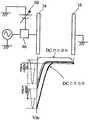
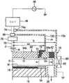
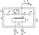
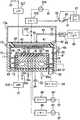
Translated fromKorean도 1은 본 발명의 실시예 1에 따른 플라즈마 에칭 장치를 나타낸 개략 단면도,1 is a schematic cross-sectional view showing a plasma etching apparatus according to
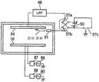
도 2는 도 1의 플라즈마 에칭 장치에 있어서 제 1 고주파 전원에 접속된 정합기의 구조를 나타내는 도면,FIG. 2 is a view showing the structure of a matcher connected to a first high frequency power supply in the plasma etching apparatus of FIG. 1;
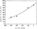
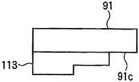
도 3은 도 1의 플라즈마 에칭 장치에 있어서, 상부 전극에 직류 전압을 인가했을 때의 Vdc 및 플라즈마 시스 두께의 변화를 나타내는 도면,3 is a view showing a change in the thickness of Vdc and plasma sheath when a direct current voltage is applied to the upper electrode in the plasma etching apparatus of FIG. 1;
도 4a는 도 1의 플라즈마 에칭 장치에 있어서, 상부 전극에 직류 전압을 인가한 경우와 인가하지 않은 경우의 플라즈마 상태를 비교하여 나타내는 도면,FIG. 4A is a diagram illustrating a plasma state in a case where a direct current voltage is applied to an upper electrode and a non-applied state in the plasma etching apparatus of FIG. 1;
도 4b는 도 1의 플라즈마 에칭 장치에 있어서, 상부 전극에 직류 전압을 인가한 경우와 인가하지 않은 경우의 플라즈마 상태를 비교하여 나타내는 도면,FIG. 4B is a view showing a plasma state in a case where a direct current voltage is applied to the upper electrode and not when the plasma etching apparatus of FIG. 1 is applied;
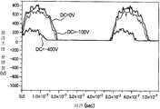
도 5는 도 1의 플라즈마 에칭 장치에 의해 상부 전극에 인가하는 직류 전압을 변화시켜 SiO2막을 에칭했을 때에 있어서의 포토레지스트막의 에칭레이트, SiO2 막의 에칭레이트, 및 포토레지스트막에 대한 Si02막의 선택비를 나타내는 그래프,5 is a Si02 film for varying the DC voltage in when etching SiO2 film is a photoresist film, the etching rate, a SiO2 film etching rate, and a photoresist film applied to the upper electrode by a plasma etching apparatus of FIG. 1 A graph showing the selectivity,
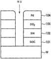
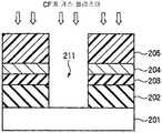
도 6은 연속 에칭 프로세스가 적용되는 다층막의 일례를 나타내는 도면,6 shows an example of a multilayer film to which a continuous etching process is applied;
도 7은 도 1의 플라즈마 에칭 장치에 있어서, 상부 전극에 직류 전압을 인가했을 때의 플라즈마 포텐셜 파형의 변화를 나타내는 도면,7 is a view showing a change in plasma potential waveform when a direct current voltage is applied to an upper electrode in the plasma etching apparatus of FIG. 1;
도 8은 도 1의 플라즈마 에칭 장치에 있어서의, 상부 전극으로 인가하는 직류 전압과 최대 플라즈마 포텐셜과의 관계를 나타내는 도면,8 is a diagram showing a relationship between a DC voltage applied to an upper electrode and a maximum plasma potential in the plasma etching apparatus of FIG. 1;
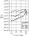
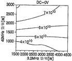
도 9는 도 1의 플라즈마 에칭 장치에 있어서, 인가하는 직류 전압을 변화시킨 경우의 전자 밀도 및 그 분포의 변화를 나타내는 도면,FIG. 9 is a diagram showing a change in electron density and its distribution when the DC voltage to be applied is changed in the plasma etching apparatus of FIG. 1; FIG.
도 10a는 도 9의 에칭에 있어서, 각 직류 전압에 있어서의 센터와 에지의 에칭 상태를 모식적으로 나타내는 도면,FIG. 10A is a diagram schematically showing an etching state between a center and an edge in each DC voltage in the etching of FIG. 9;
도 10b는 도 9의 에칭에 있어서, 각 직류 전압에 있어서의 센터와 에지의 에칭 상태를 모식적으로 나타내는 도면,FIG. 10B is a diagram schematically showing an etching state between a center and an edge in each DC voltage in the etching of FIG. 9;
도 10c는 도 9의 에칭에 있어서, 각 직류 전압에 있어서의 센터와 에지의 에칭 상태를 모식적으로 나타내는 도면,FIG. 10C is a diagram schematically showing an etching state between a center and an edge in each DC voltage in the etching of FIG. 9;
도 11은 상부 전극 표면에 있어서의 자기 바이어스 전압과, 인가하는 직류 전압과의 관계를 나타내는 도면,11 is a diagram illustrating a relationship between a self bias voltage on a surface of an upper electrode and a DC voltage to be applied;
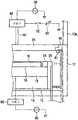
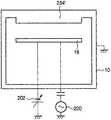
도 12는 도 1의 플라즈마 에칭 장치에 있어서, 플라즈마를 검출하는 검출기를 마련한 상태를 나타내는 단면도,12 is a cross-sectional view showing a state in which a detector for detecting plasma is provided in the plasma etching apparatus of FIG. 1;
도 13은 도 1의 플라즈마 에칭 장치에 있어서, 상부 전극으로 직류 전압을 인가할 때에 이상(異常) 방전을 억제하기 위한 파형을 나타내는 도면,FIG. 13 is a diagram showing waveforms for suppressing abnormal discharge when the direct current voltage is applied to the upper electrode in the plasma etching apparatus of FIG. 1; FIG.
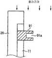
도 14는 GND 블록의 다른 배치예를 나타내는 개략도,14 is a schematic diagram showing another arrangement example of a GND block;
도 15는 GND 블록의 또 다른 배치예를 나타내는 개략도,15 is a schematic view showing still another example of arrangement of a GND block;
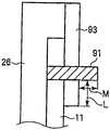
도 16a는 GND 블록의 부착물 방지예를 설명하기 위한 도면,16A is a view for explaining an example of preventing deposits on a GND block;
도 16b는 GND 블록의 부착물 방지예를 설명하기 위한 도면,16B is a view for explaining an example of preventing deposits on the GND block;
도 17은 GND 블록의 부착물을 제거할 수 있는 장치 구성의 일례를 나타내는 개략도,17 is a schematic diagram showing an example of a device configuration capable of removing a deposit of a GND block;
도 18a는 도 17의 장치에 있어서의 플라즈마 에칭시에 있어서의 상태와 클리닝시에 있어서의 상태를 설명하기 위한 개략도,18A is a schematic diagram for explaining a state during plasma etching and a state during cleaning in the apparatus of FIG. 17;
도 18b는 도 17의 장치에 있어서의 플라즈마 에칭시에 있어서의 상태와 클리닝시에 있어서의 상태를 설명하기 위한 개략도,18B is a schematic diagram for explaining a state during plasma etching and a state during cleaning in the apparatus of FIG. 17;
도 19는 도 17의 장치에 있어서의 플라즈마 에칭시에 있어서의 다른 상태를 나타내는 개략도,19 is a schematic view showing another state during plasma etching in the apparatus of FIG. 17;
도 20은 GND 블록의 부착물을 제거할 수 있는 장치 구성의 다른 예를 나타내는 개략도,20 is a schematic diagram showing another example of an apparatus configuration capable of removing an attachment of a GND block;
도 21a는 도 20의 장치에 있어서의 플라즈마 에칭시에 있어서의 상태와 클리닝시에 있어서의 상태를 설명하기 위한 개략도,FIG. 21A is a schematic diagram for explaining a state during plasma etching and a state during cleaning in the apparatus of FIG. 20; FIG.
도 21b는 도 20의 장치에 있어서의 플라즈마 에칭시에 있어서의 상태와 클리닝시에 있어서의 상태를 설명하기 위한 개략도,21B is a schematic diagram for explaining a state during plasma etching and a state during cleaning in the apparatus of FIG. 20;
도 22는 DC적으로 접지되지 않게 되는 것을 방지하는 기능을 구비한 GND 블록의 일례를 나타내는 모식도,22 is a schematic diagram showing an example of a GND block having a function of preventing the DC from being grounded;
도 23은 DC적으로 접지되지 않게 되는 것을 방지하는 기능을 구비한 GND 블 록의 다른 예를 나타내는 모식도,23 is a schematic diagram illustrating another example of a GND block having a function of preventing the DC from being grounded;
도 24a는 DC적으로 접지되지 않게 되는 것을 방지하는 기능을 구비한 GND 블록의 또 다른 예를 나타내는 모식도,24A is a schematic diagram illustrating still another example of a GND block having a function of preventing DC grounding;
도 24b는 DC적으로 접지되지 않게 되는 것을 방지하는 기능을 구비한 GND 블록의 또 다른 예를 나타내는 모식도,24B is a schematic diagram illustrating still another example of a GND block having a function of preventing DC grounding;
도 25는 DC적으로 접지되지 않게 되는 것을 방지하는 기능을 구비한 GND 블록의 또 다른 예를 나타내는 모식도,25 is a schematic diagram illustrating still another example of a GND block having a function of preventing the DC from being grounded;
도 26은 DC적으로 접지되지 않게 되는 것을 방지하는 기능을 구비한 GND 블록의 또 다른 예를 나타내는 모식도,FIG. 26 is a schematic diagram illustrating still another example of a GND block having a function of preventing DC grounding; FIG.
도 27은 DC적으로 접지되지 않게 되는 것을 방지하는 기능을 구비한 GND 블록의 또 다른 예를 나타내는 모식도,FIG. 27 is a schematic diagram illustrating still another example of a GND block having a function of preventing DC grounding; FIG.
도 28은 RF 플라즈마 및 DC 플라즈마에 있어서의 전자 온도 분포를 나타내는 도면,28 shows electron temperature distribution in an RF plasma and a DC plasma;
도 29는 고주파 전력만으로 플라즈마를 형성한 경우와 직류 전압도 인가한 경우에 있어서의 전자 온도 분포를 나타내는 도면,29 is a diagram showing an electron temperature distribution when a plasma is formed using only high frequency power and a DC voltage is also applied;
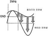
도 30a는 바이어스 고주파 전력의 주파수가 2㎒인 경우와 13.56㎒인 경우에 있어서의 이온의 추종성을 설명하기 위한 도면,30A is a diagram for explaining the followability of ions when the frequency of the bias high frequency power is 2 MHz and when the frequency is 13.56 MHz;
도 30b는 바이어스 고주파 전력의 주파수가 2㎒인 경우와 13.56㎒인 경우에 있어서의 이온의 추종성을 설명하기 위한 도면,30B is a diagram for explaining the followability of ions when the frequency of the bias high frequency power is 2 MHz and when the frequency is 13.56 MHz;
도 31은 바이어스 고주파 전력의 주파수가 2㎒인 경우와 13.56㎒인 경우에 있어서의 이온 에너지 분포를 나타내는 도면,31 is a diagram showing an ion energy distribution when the frequency of the bias high frequency power is 2 MHz and when the frequency is 13.56 MHz;
도 32a는 도 1의 플라즈마 에칭 장치에 의해 에칭을 행할 때에 있어서의 에칭 대상으로 될 수 있는 웨이퍼의 단면 구조의 일례를 나타내는 모식도,32A is a schematic diagram illustrating an example of a cross-sectional structure of a wafer that can be an etching target when etching is performed by the plasma etching apparatus of FIG. 1;
도 32b는 도 1의 플라즈마 에칭 장치에 의해 에칭을 행할 때에 있어서의 에칭 대상으로 될 수 있는 웨이퍼의 단면 구조의 일례를 나타내는 모식도,32B is a schematic diagram illustrating an example of a cross-sectional structure of a wafer that may be an etching target when etching is performed by the plasma etching apparatus of FIG. 1;
도 33a는 도 1의 플라즈마 에칭 장치에 의해 에칭을 행할 때에 있어서의 에칭 대상으로 될 수 있는 웨이퍼의 단면 구조의 다른 예를 나타내는 모식도,33A is a schematic diagram illustrating another example of a cross-sectional structure of a wafer that can be an etching target when etching is performed by the plasma etching apparatus of FIG. 1;
도 33b는 도 1의 플라즈마 에칭 장치에 의해 에칭을 행할 때에 있어서의 에칭 대상으로 될 수 있는 웨이퍼의 단면 구조의 다른 예를 나타내는 모식도,33B is a schematic diagram illustrating another example of a cross-sectional structure of a wafer that can be an etching target when etching is performed by the plasma etching apparatus of FIG. 1.
도 34는 본 발명의 실시예 2에 따른 플라즈마 에칭 장치를 나타내는 개략 단면도,34 is a schematic cross-sectional view showing a plasma etching apparatus according to a second embodiment of the present invention;
도 35는 도 34의 플라즈마 에칭 장치의 주요부의 구성을 나타내는 개략 단면도,FIG. 35 is a schematic cross-sectional view showing a configuration of main parts of the plasma etching apparatus of FIG. 34; FIG.
도 36은 도 34의 플라즈마 에칭 장치에 있어서의 플라즈마 생성 수단의 주요부의 등가 회로를 나타내는 회로도,36 is a circuit diagram showing an equivalent circuit of a main part of the plasma generating means in the plasma etching apparatus of FIG. 34;
도 37은 도 34의 플라즈마 에칭 장치에 있어서의 가변 콘덴서의 캐패시턴스의 값과 전계 강도 비율과의 관계를 나타내는 도면,FIG. 37 is a view showing a relationship between a capacitance value of a variable capacitor and an electric field intensity ratio in the plasma etching apparatus of FIG. 34; FIG.
도 38은 도 34의 플라즈마 에칭 장치의 상부 전극으로의 직류 전압 인가의 변형예를 나타내는 도면,FIG. 38 is a view showing a modification of DC voltage application to the upper electrode of the plasma etching apparatus of FIG. 34;
도 39는 도 34의 플라즈마 에칭 장치의 상부 전극으로의 직류 전압 인가의 다른 변형예를 나타내는 도면,FIG. 39 shows another modification of the application of the DC voltage to the upper electrode of the plasma etching apparatus of FIG. 34;
도 40은 본 발명의 실시예 3에 따른 플라즈마 에칭 장치를 나타내는 개략 단면도,40 is a schematic cross-sectional view showing a plasma etching apparatus according to a third embodiment of the present invention;
도 41은 본 발명의 실시예 3에 따른 플라즈마 에칭 장치를 나타내는 개략 단면도,41 is a schematic cross-sectional view showing a plasma etching apparatus according to a third embodiment of the present invention;
*도 42a는 도 41의 플라즈마 에칭 장치에 있어서, 상부 전극에 직류 전압을 인가했을 때의 Vdc 및 플라즈마 시스 두께의 변화를 나타내는 도면,Fig. 42A is a view showing changes in Vdc and plasma sheath thicknesses when a DC voltage is applied to the upper electrode in the plasma etching apparatus of Fig. 41;
도 42b는 도 41의 플라즈마 에칭 장치에 있어서, 상부 전극에 직류 전압을 인가했을 때의 Vdc 및 플라즈마 시스 두께의 변화를 나타내는 도면,FIG. 42B is a view showing changes in Vdc and plasma sheath thickness when a DC voltage is applied to the upper electrode in the plasma etching apparatus of FIG. 41;
도 43a는 도 41의 플라즈마 에칭 장치에 있어서, HARC 에칭의 조건을 이용하여, 인가하는 직류 전압을 변화시킨 경우의 전자 밀도의 변화를 나타내는 도면,FIG. 43A is a diagram showing a change in electron density when the DC voltage to be applied is changed by using a condition of HARC etching in the plasma etching apparatus of FIG. 41;
도 43b는 도 41의 플라즈마 에칭 장치에 있어서, HARC 에칭의 조건을 이용하여, 인가하는 직류 전압을 변화시킨 경우의 전자 밀도의 변화를 나타내는 도면,FIG. 43B is a diagram showing a change in electron density when the DC voltage to be applied is changed by using a condition of HARC etching in the plasma etching apparatus of FIG. 41;
도 43c는 도 41의 플라즈마 에칭 장치에 있어서, HARC 에칭의 조건을 이용하여, 인가하는 직류 전압을 변화시킨 경우의 전자 밀도의 변화를 나타내는 도면,FIG. 43C is a diagram showing a change in electron density when the DC voltage to be applied is changed using the condition of HARC etching in the plasma etching apparatus of FIG. 41;
도 43d는 도 41의 플라즈마 에칭 장치에 있어서, HARC 에칭의 조건을 이용하여, 인가하는 직류 전압을 변화시킨 경우의 전자 밀도의 변화를 나타내는 도면,FIG. 43D is a diagram showing a change in electron density when the DC voltage to be applied is changed by using a condition of HARC etching in the plasma etching apparatus of FIG. 41;
도 44a는 도 41의 플라즈마 에칭 장치에 있어서, Via 에칭의 조건을 이용하 여, 인가하는 직류 전압을 변화시킨 경우의 전자 밀도의 변화를 나타내는 도면,FIG. 44A is a diagram showing a change in electron density when the DC voltage to be applied is changed using the conditions of Via etching in the plasma etching apparatus of FIG. 41;
도 44b는 도 41의 플라즈마 에칭 장치에 있어서, Via 에칭의 조건을 이용하여, 인가하는 직류 전압을 변화시킨 경우의 전자 밀도의 변화를 나타내는 도면,FIG. 44B is a view showing a change in electron density when the DC voltage to be applied is changed using the Via etching condition in the plasma etching apparatus of FIG. 41;
도 44c는 도 41의 플라즈마 에칭 장치에 있어서, Via 에칭의 조건을 이용하여, 인가하는 직류 전압을 변화시킨 경우의 전자 밀도의 변화를 나타내는 도면,FIG. 44C is a diagram showing a change in electron density when the DC voltage to be applied is changed using the Via etching condition in the plasma etching apparatus of FIG. 41;
도 44d는 도 41의 플라즈마 에칭 장치에 있어서, Via 에칭의 조건을 이용하여, 인가하는 직류 전압을 변화시킨 경우의 전자 밀도의 변화를 나타내는 도면,FIG. 44D is a diagram showing a change in electron density when the DC voltage to be applied is changed using the Via etching condition in the plasma etching apparatus of FIG. 41;
도 45는 상기 HARC 에칭에서, 제 1 고주파 전력을 3000W, 제 2 고주파 전력을 4000W로 한 경우의 웨이퍼 직경 방향의 전자 밀도 분포를 나타내는 도면,45 is a diagram showing an electron density distribution in the wafer radial direction when the first high frequency power is 3000W and the second high frequency power is 4000W in the HARC etching;
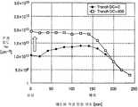
도 46은 트렌치 에칭의 조건을 이용하여, 직류 전압을 인가한 경우와 인가하지 않은 경우에 있어서 웨이퍼 직경 방향의 전자 밀도 분포를 측정한 결과를 나타내는 도면,FIG. 46 shows the results of measuring the electron density distribution in the wafer radial direction when a direct current voltage was applied or not, using the conditions of trench etching; FIG.
도 47은 도 41의 플라즈마 에칭 장치에 있어서의, 상부 전극의 전기적 상태를 나타내는 도면,FIG. 47 is a view showing an electrical state of an upper electrode in the plasma etching apparatus of FIG. 41;
도 48은 도 41의 플라즈마 에칭 장치에 있어서의, 상부 전극의 전기적 상태를 나타내는 도면,FIG. 48 shows the electrical state of the upper electrode in the plasma etching apparatus of FIG. 41;
도 49는 도 41의 플라즈마 에칭 장치에 있어서의, 상부 전극의 전기적 상태를 나타내는 도면,FIG. 49 shows the electrical state of the upper electrode in the plasma etching apparatus of FIG. 41;
도 50은 도 41의 플라즈마 에칭 장치에 있어서, 플라즈마를 검출하는 검출기를 마련한 상태를 나타내는 단면도,50 is a cross-sectional view showing a state where a detector for detecting plasma is provided in the plasma etching apparatus of FIG. 41;
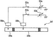
도 51은 GND 블록의 다른 배치예를 나타내는 개략도,51 is a schematic diagram illustrating another arrangement example of a GND block;
도 52는 GND 블록의 또 다른 배치예를 나타내는 개략도,52 is a schematic diagram showing another layout example of a GND block;
도 53은 GND 블록의 부착물을 제거할 수 있는 장치 구성의 일례를 나타내는 개략도,53 is a schematic diagram showing an example of a device configuration capable of removing a deposit on a GND block;
도 54a는 도 53의 장치에 있어서의 플라즈마 에칭시에 있어서의 상태와 클리닝시에 있어서의 상태를 설명하기 위한 개략도,FIG. 54A is a schematic diagram for explaining a state during plasma etching and a state during cleaning in the apparatus of FIG. 53; FIG.
도 54b는 도 53의 장치에 있어서의 플라즈마 에칭시에 있어서의 상태와 클리닝시에 있어서의 상태를 설명하기 위한 개략도,FIG. 54B is a schematic diagram for explaining a state during plasma etching and a state during cleaning in the apparatus of FIG. 53; FIG.
도 55는 도 53의 장치에 있어서의 플라즈마 에칭시에 있어서의 다른 상태를 나타내는 개략도,55 is a schematic view showing another state during plasma etching in the apparatus of FIG. 53;
도 56은 GND 블록의 부착물을 제거할 수 있는 장치 구성의 다른 예를 나타내는 개략도,56 is a schematic diagram showing another example of the apparatus configuration capable of removing the attachment of the GND block;
도 57a는 도 56의 장치에 있어서의 플라즈마 에칭시에 있어서의 상태와 클리닝시에 있어서의 상태를 설명하기 위한 개략도,FIG. 57A is a schematic diagram for explaining a state during plasma etching and a state during cleaning in the apparatus of FIG. 56; FIG.
도 57b는 도 56의 장치에 있어서의 플라즈마 에칭시에 있어서의 상태와 클리닝시에 있어서의 상태를 설명하기 위한 개략도,FIG. 57B is a schematic diagram for explaining a state during plasma etching and a state during cleaning in the apparatus of FIG. 56; FIG.
도 58은 본 발명의 실시예 4에 따른 플라즈마 에칭 장치의 주요부를 간략화하여 나타내는 개략 단면도,58 is a schematic sectional view schematically showing a main part of a plasma etching apparatus according to Embodiment 4 of the present invention;
도 59는 본 발명의 실시예 5에 따른 플라즈마 에칭 장치의 주요부를 간략화하여 나타내는 개략 단면도,59 is a schematic sectional view schematically showing a main part of a plasma etching apparatus according to
도 60은 본 발명의 실시예 6에 따른 플라즈마 에칭 장치의 주요부를 간략화하여 나타내는 단면도,60 is a sectional view schematically showing a main part of a plasma etching apparatus according to a sixth embodiment of the present invention;
도 61은 본 발명의 실시예 7에 따른 플라즈마 에칭 장치의 주요부를 간략화하여 나타내는 단면도,61 is a sectional view schematically showing a main part of a plasma etching apparatus according to a seventh embodiment of the present invention;
도 62는 본 발명의 실시예 8에 따른 플라즈마 에칭 장치의 주요부를 간략화하여 나타내는 단면도,Fig. 62 is a sectional view schematically showing a main part of a plasma etching apparatus according to Embodiment 8 of the present invention;
도 63은 본 발명의 실시예 9에 따른 플라즈마 에칭 장치의 주요부를 간략화하여 나타내는 단면도,FIG. 63 is a sectional view schematically showing a main part of a plasma etching apparatus according to Embodiment 9 of the present invention; FIG.
도 64는 본 발명의 실시예 10에 따른 플라즈마 에칭 장치의 주요부를 간략화하여 나타내는 단면도,64 is a sectional view schematically showing a main part of a plasma etching apparatus according to a tenth embodiment of the present invention;
도 65는 본 발명의 실시예 11에 따른 플라즈마 에칭 장치의 주요부를 간략화하여 나타내는 단면도,65 is a sectional view schematically showing a main part of a plasma etching apparatus according to
도 66은 본 발명의 실시예 12에 따른 플라즈마 에칭 장치의 주요부를 간략화하여 나타내는 단면도,66 is a sectional view schematically showing a main part of a plasma etching apparatus according to a twelfth embodiment of the present invention;
도 67은 본 발명의 실시예 13에 따른 플라즈마 에칭 장치의 주요부를 간략화하여 나타내는 개략 단면도,67 is a schematic sectional view schematically showing a main part of a plasma etching apparatus according to a thirteenth embodiment of the present invention;
도 68은 본 발명의 실시예 13에 따른 플라즈마 에칭 장치와 대비할 만한 종래의 플라즈마 에칭 장치의 주요부를 간략화하여 나타내는 개략 단면도,FIG. 68 is a schematic sectional view schematically showing a main part of a conventional plasma etching apparatus that is contrasted with the plasma etching apparatus according to
도 69는 본 발명의 실시예 13에 따른 플라즈마 에칭 장치의 변형예의 주요부를 간략화하여 나타내는 개략 단면도,69 is a schematic sectional view schematically showing a main part of a modification of the plasma etching apparatus according to
도 70은 본 발명의 실시예 13에 따른 플라즈마 에칭 장치의 다른 변형예의 주요부를 간략화하여 나타내는 단면도,70 is a sectional view schematically showing a main part of another modification of the plasma etching apparatus according to the thirteenth embodiment of the present invention;
도 71은 본 발명의 실시예 13에 따른 플라즈마 에칭 장치의 다른 변형예의 주요부를 간략화하여 나타내는 개략 단면도,71 is a schematic sectional view schematically showing a main part of another modification of the plasma etching apparatus according to the thirteenth embodiment of the present invention;
도 72는 본 발명의 실시예 13에 따른 플라즈마 에칭 장치의 또 다른 변형예의 주요부를 나타내는 개략 단면도,72 is a schematic sectional view showing a main part of still another modification of the plasma etching apparatus according to
도 73은 본 발명의 실시예 13에 따른 플라즈마 에칭 장치의 또 다른 변형예의 주요부를 나타내는 개략 단면도,73 is a schematic sectional view showing the principal parts of still another modification of the plasma etching apparatus according to the thirteenth embodiment of the present invention;
도 74는 본 발명의 실시예 14에 따른 플라즈마 에칭 장치의 주요부를 간략화하여 나타내는 단면도,74 is a sectional view schematically showing a main part of a plasma etching apparatus according to
도 75는 본 발명의 실시예 14에 따른 플라즈마 에칭 장치의 변형예의 주요부를 간략화하여 나타내는 개략 단면도,75 is a schematic sectional view schematically showing a main part of a modification of the plasma etching apparatus according to
도 76은 본 발명의 실시예 15에 따른 플라즈마 에칭 장치의 주요부를 간략화하여 나타내는 개략 단면도,76 is a schematic sectional view schematically showing a main part of a plasma etching apparatus according to a fifteenth embodiment of the present invention;
도 77은 본 발명의 실시예 15에 따른 플라즈마 에칭 장치의 변형예의 주요부를 간략화하여 나타내는 개략 단면도,77 is a schematic sectional view schematically showing a main part of a modification of the plasma etching apparatus according to Embodiment 15 of the present invention;
도 78은 본 발명의 실시예 15에 따른 플라즈마 에칭 장치의 다른 변형예의 주요부를 간략화하여 나타내는 개략 단면도,78 is a schematic sectional view schematically showing a main part of another modification of the plasma etching apparatus according to the fifteenth embodiment of the present invention;
도 79는 본 발명의 실시예 16에 따른 플라즈마 에칭 장치의 예를 나타내는 단면도,79 is a sectional view showing an example of the plasma etching apparatus according to the sixteenth embodiment of the present invention;
도 80은 본 발명의 실시예 17에 따른 플라즈마 에칭 장치의 예를 나타내는 단면도,80 is a sectional view showing an example of a plasma etching apparatus according to
도 81은 본 발명을 적용할 수 있는 다른 타입의 플라즈마 에칭 장치의 예를 나타내는 단면도,81 is a sectional view showing an example of another type of plasma etching apparatus to which the present invention can be applied;
도 82는 본 발명을 적용할 수 있는 또 다른 타입의 플라즈마 에칭 장치의 예를 나타내는 개략도이다.82 is a schematic view showing an example of another type of plasma etching apparatus to which the present invention can be applied.
도면의 주요 부분에 대한 부호의 설명Explanation of symbols for the main parts of the drawings
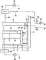
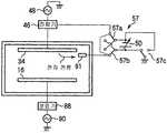
51 : 컨트롤러66 : 처리 가스 공급원51
84 : 배기 장치87 :정합기84
89 : 정합기95 : 제어부89: matching device 95: control unit
96 : 사용자 인터페이스97 : 기억부96: user interface 97: storage unit
본 발명은 반도체 기판 등의 피처리 기판에 플라즈마 처리를 실시하는 플라즈마 처리 장치, 플라즈마 처리 방법, 및 컴퓨터 판독 가능한 기억 매체에 관한 것이다.BACKGROUND OF THE
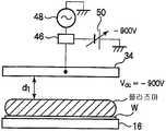
예컨대, 반도체 장치의 제조 프로세스에 있어서는, 피처리 기판인 반도체 웨 이퍼에 형성된 소정의 층에 소정의 패턴을 형성하기 위해, 레지스트를 마스크로 하여 플라즈마에 의해 에칭하는 플라즈마 에칭 처리가 많이 이용되고 있다.For example, in the manufacturing process of a semiconductor device, in order to form a predetermined | prescribed pattern in the predetermined | prescribed layer formed in the semiconductor wafer which is a to-be-processed substrate, the plasma etching process which etches by plasma using a resist as a mask is used a lot.
이러한 플라즈마 에칭을 행하기 위한 플라즈마 에칭 장치로는, 여러 가지의 것이 이용되고 있지만, 그 중에서도 용량 결합형 평행 평판 플라즈마 처리 장치가 주류를 이루고 있다.As a plasma etching apparatus for performing such plasma etching, various things are used, but the capacitively coupled parallel plate plasma processing apparatus is the mainstream among them.
용량 결합형 평행 평판 플라즈마 에칭 장치는, 챔버 내에 한 쌍의 평행 평판 전극(상부 및 하부 전극)을 배치하고, 처리 가스를 챔버 내에 도입하는 동시에, 전극의 한쪽에 고주파를 인가하여 전극 사이에 고주파 전계를 형성하고, 이 고주파 전계에 의해 처리 가스인 플라즈마를 형성하여 반도체 웨이퍼의 소정의 층에 대해 플라즈마 에칭을 실시한다.The capacitively coupled parallel plate plasma etching apparatus arranges a pair of parallel plate electrodes (upper and lower electrodes) in a chamber, introduces a processing gas into the chamber, and applies a high frequency to one of the electrodes to apply a high frequency electric field between the electrodes. Is formed, a plasma which is a processing gas is formed by this high frequency electric field, and plasma etching is performed on a predetermined layer of the semiconductor wafer.
구체적으로는, 상부 전극에 플라즈마 형성용 고주파를 인가하여 플라즈마를 형성하고, 하부 전극에 이온 인입용 고주파를 인가함으로써, 적절한 플라즈마 상태를 형성하는 플라즈마 에칭 장치가 알려져 있으며, 이에 따라, 고(高) 선택비로 재현성이 높은 에칭 처리가 가능하다(예컨대, 일본 공개 특허 공보 제 2000-173993호(특허문헌 1)).Specifically, a plasma etching apparatus is known which forms an appropriate plasma state by applying a high frequency for plasma formation to an upper electrode to form a plasma, and applying a high frequency for ion induction to a lower electrode, whereby a high plasma state is known. Etching process with high reproducibility is possible at a selection ratio (for example, Unexamined-Japanese-Patent No. 2000-173993 (patent document 1)).
그런데, 최근의 미세 가공의 요구에 대응하여, 마스크로서 이용되는 포토레지스트의 막두께가 얇아져서, 사용되는 포토레지스트도 KrF 포토레지스트(즉, KrF 가스를 발광원으로 한 레이저광으로 노광하는 포토레지스트)에서, 약 0.13㎛ 이하의 패턴 개구를 형성할 수 있는 ArF 포토레지스트(즉, ArF 가스를 발광원으로 한, 보다 단파장의 레이저광으로 노광하는 포토레지스트)로 이행되고 있다.By the way, in response to the recent demand for microfabrication, the film thickness of the photoresist used as a mask becomes thin, so that the photoresist used is also exposed to KrF photoresist (that is, photoresist exposed by laser light using KrF gas as a light emitting source). ), An ArF photoresist capable of forming a pattern opening of about 0.13 μm or less (that is, a photoresist exposed with a shorter wavelength laser light using ArF gas as a light emitting source).
그러나, ArF 포토레지스트는 내(耐)플라즈마성이 낮기 때문에, KrF 레지스트에서는 거의 발생하지 않았던 에칭 도중에서의 표면의 거칠기(roughness)가 발생되게 된다고 하는 문제가 있다. 이 때문에, 개구부의 내벽면에 세로줄(스트라이에이션(striation))이 생기거나, 개구부가 넓어지는(CD의 확대) 등의 문제가 발생하여, 포토레지스트의 막두께가 얇은 것과 더해져서, 양호한 에칭 선택비로 에칭 홀을 형성할 수가 없다고 하는 문제가 발생하고 있다.However, since ArF photoresist has low plasma resistance, there is a problem that roughness of the surface is generated during etching which hardly occurred in KrF resist. This causes problems such as vertical streaks (striation) on the inner wall surface of the openings, widening of the openings (expansion of the CD), and a thin film thickness of the photoresist. There arises a problem that an etching hole cannot be formed.
한편, 이러한 종류의 에칭 장치에서는, 상부 전극에 공급한 플라즈마 생성용의 고주파 전력의 파워가 작은 경우에는, 에칭 종료 후에 상부 전극에 퇴적물(데포지션(deposition))이 부착되어, 프로세스 특성의 변화나 파티클(particle)의 우려가 있다. 또한, 파워가 큰 경우에는, 전극의 마모가 발생하여, 파워가 작은 경우와는 프로세스 특성이 변화한다. 고주파 전원으로부터의 파워는 프로세스에 따라 적정한 범위가 결정되기 때문에, 어떠한 파워에서도 프로세스가 변동되지 않는 것이 바람직하다. 또한, 에칭시에는 챔버 벽에 데포지션이 발생하여, 연속 에칭 프로세스의 경우 등에 있어서, 앞의 처리의 영향이 잔존하여 다음 처리에 악영향을 미치는 메모리 효과가 발생하기 때문에, 챔버 벽에의 퇴적물의 부착 해소도 요구된다.On the other hand, in this kind of etching apparatus, when the power of the high frequency power for plasma generation supplied to the upper electrode is small, a deposit (deposition) adheres to the upper electrode after the end of etching, resulting in a change in process characteristics and There is a fear of particles. In addition, when the power is large, wear of the electrode occurs, and the process characteristics change when the power is small. Since the power from the high frequency power source is determined in an appropriate range depending on the process, it is preferable that the process does not vary at any power. In addition, deposition occurs on the chamber wall during etching, and in the case of a continuous etching process, for example, in the case of a continuous etching process, since the effect of the previous process remains and a memory effect that adversely affects the next process occurs, deposition of deposits on the chamber wall is caused. Resolution is also required.
또한, 이러한 평행 평판형 용량 결합형의 에칭 장치에서는, 챔버 내의 압력이 높고 사용하는 에칭 가스가 부성(負性) 가스(예컨대, CxFy, O2 등)의 경우에, 챔버 중심부의 플라즈마 밀도가 낮아지는데, 이러한 경우에 플라즈마 밀도를 컨트롤 하는 것은 곤란하다.In addition, in such a parallel plate capacitively coupled etching apparatus, when the pressure in the chamber is high and the etching gas to be used is a negative gas (for example, Cx Fy , O2, etc.), the plasma at the center of the chamber is used. The density is lowered, in which case it is difficult to control the plasma density.
한편, 반도체 장치에 있어서, 배선의 미세화나 고속화의 요구가 높아짐에 수반하여, 배선 기생 용량의 저감을 도모할 목적으로 저유전율의 층간 절연막의 이용이 진행되고 있다. 이러한 저유전율막(Low-k막) 중에서도, 특히 SiOC계 막이 주목을 받고 있다.In the semiconductor device, on the other hand, as the demand for miniaturization and high speed of wiring increases, the use of a low dielectric constant interlayer insulating film is progressing in order to reduce wiring parasitic capacitance. Among such low dielectric constant films (Low-k films), SiOC films are particularly attracting attention.
SiOC계 막 등의 유기계 Low-k막에 플라즈마 에칭을 행하는 경우, 중요시되는 것이 질화규소 등의 하지막(下地膜)이나 마스크층과의 선택비를 충분히 확보하는 것이다. 통상은, 하지막과의 선택성이 비교적 높은 처리 가스로서 플루오로카본 가스계의 혼합 가스가 이용되지만, 그것만으로 충분한 선택비를 얻기는 어렵다. 그래서, SiOC계 막의 에칭에 있어서, Cu 배선의 배리어층인 질화규소막을 하지 에치 스톱층으로 하여 SiOC계 층간 절연막을 플라즈마 에칭할 때에, 하지막과의 선택비를 향상시키기 위하여, 처리 가스로서 C4F8/Ar/N2를 Ar의 유량비가 80% 이상으로 되도록 이용하여, 질화규소막과의 선택비를 향상시키는 에칭 방법이 제안되어 있다(예컨대, 일본 공개 특허 공보 제 2002-270586호(특허문헌 2)).In the case of performing plasma etching on an organic low-k film such as an SiOC film, it is important to sufficiently secure a selectivity with an underlying film such as silicon nitride or a mask layer. Usually, although the mixed gas of a fluorocarbon gas system is used as a process gas with a relatively high selectivity with a base film, it is difficult to obtain sufficient selectivity only by it. Therefore, in etching the SiOC film, in order to improve the selectivity with the underlying film when plasma etching the SiOC interlayer insulating film using the silicon nitride film as the barrier layer of the Cu wiring as the base etch stop layer, C4 F is used as the processing gas. is8 / with such an Ar / N2 in a flow rate ratio of 80% or more of Ar, the etching method for improving the selectivity of the silicon nitride film has been proposed (e.g., Japanese Laid-Open Patent Publication No. 2002-270586 (Patent Document 2 )).
또한, 상기 특허문헌 2와 마찬가지로, 질화규소막을 하지 에치 스톱층으로 하여 SiOC계 층간 절연막을 플라즈마 에칭할 때에, 처리 가스로서 CHF3/Ar/N2를 이용하는 제 1 단계의 에칭과, 처리 가스로서 C4F8/Ar/N2를 이용하는 제 2 단계의 에칭을 행하여, 마스크와 질화규소막의 양쪽에 대한 선택비를 향상시키는 에칭 방법도 제안되어 있다(예컨대, 일본 공개 특허 공보 제 2004-87875호(특허문헌 3))In addition, as in Patent Document 2, when not silicon nitride film by the etch stop layer to plasma etch the SiOC-based inter-layer insulating film, a process gas CHF3 / Ar / N etching of the first step using thesecond and, as the process gas C4, etching is performed in a second stage using an F8 / Ar / N2, the etching method for improving the selectivity to the both sides of the mask and the silicon nitride film has been proposed (e.g., Japanese Laid-Open Patent Publication No. 2004-87875 (Patent Document 3))
그러나, 전술한 바와 같이 Cu 배선의 배리어층으로서 이용되고 있는 질화규소는 배리어성은 좋지만, 비유전률이 7.0으로 높기 때문에, SiOC계 막 등의 Low-k막의 저유전율 특성을 충분히 활용하기 위해서는, 비유전률이 더욱 낮은 배리어층이 요구되고 있으며, 그 하나로서 비유전률이 3.5인 탄화규소(SiC)가 있다.However, as described above, silicon nitride used as a barrier layer for Cu wiring has good barrier properties, but has a high dielectric constant of 7.0. Therefore, in order to fully utilize the low dielectric constant characteristics of low-k films such as SiOC films, Lower barrier layers are required, one of which is silicon carbide (SiC) having a relative dielectric constant of 3.5.
이러한 저유전율 배리어층인 SiC를 하지 에치 스톱층으로서 사용하여 상층의 피에칭층인 Low-k막을 에칭할 때에 있어서도, 충분한 에칭 선택비를 확보하는 것이 필요하다. 그러나, 상기 특허문헌 2 및 특허문헌 3에 기재된 플루오로카본계의 처리 가스를 이용하는 플라즈마 에칭에서는, Low-k막과 SiC층과의 에칭 선택비를 충분히 확보할 수가 없다.Even when etching the Low-k film which is an upper etching target layer using SiC which is such a low dielectric constant barrier layer as a base etch stop layer, it is necessary to ensure sufficient etching selectivity. However, in the plasma etching using the fluorocarbon process gas of patent document 2 and
본 발명은 이러한 사정을 감안하여 이루어진 것으로, 레지스트층 등의 유기 마스크층의 내(耐)플라즈마성을 높게 유지하여 고(高)선택비로 에칭할 수 있고, 또는 전극으로의 퇴적물의 부착을 유효하게 해소할 수 있으며, 또는 고속의 에칭이 가능하고, 또는 피처리 기판에 대하여 균일한 에칭을 행할 수 있는 플라즈마 처리 장치 및 플라즈마 처리 방법을 제공하는 것을 목적으로 한다.SUMMARY OF THE INVENTION The present invention has been made in view of the above circumstances, and can be etched at a high selectivity while maintaining high plasma resistance of organic mask layers such as a resist layer, or effectively depositing deposits on electrodes. It is an object of the present invention to provide a plasma processing apparatus and a plasma processing method capable of eliminating the problem, enabling high speed etching, or performing uniform etching on a substrate to be processed.
또한, 에치 스톱층으로서의 하지 SiC층에 대하여 높은 에칭 선택비로 Low-k막의 에칭을 행할 수 있는 플라즈마 처리 방법을 제공하는 것을 목적으로 한다.Moreover, it aims at providing the plasma processing method which can etch a low-k film with a high etching selectivity with respect to the base SiC layer as an etch stop layer.
본 발명의 제 1 관점에서는, 피처리 기판이 수용되고, 진공 배기 가능한 처리 용기와, 처리 용기 내에 대향하여 배치되는 제 1 전극 및 제 2 전극과, 상기 제 1 전극 또는 제 2 전극에 플라즈마 형성용 제 1 고주파 전력을 공급하는 제 1 고주파 전력 공급 유닛과, 상기 처리 용기 내에 처리 가스를 공급하는 처리 가스 공급 유닛을 구비하고, 상기 제 1 전극 및 제 2 전극과의 사이에 처리 가스인 플라즈마를 생성하여 피처리 기판의 소정의 층을 플라즈마 처리하는 플라즈마 처리 장치로서, 상기 제 1 전극 또는 제 2 전극에 직류 전압 또는 교류 전압을 인가하는 전원을 더 구비하고, 인가 전극의 표면에 대한 소정의 스퍼터 효과를 얻을 수 있는 정도로 그 표면의 자기 바이어스 전압 Vdc의 절대값이 커지도록, 또는 인가 전극에 있어서의 플라즈마 시스(sheath)의 두께를 확대시켜, 상기 인가 전극의 대향 전극측에 축소된 플라즈마가 형성되도록, 또는 인가 전극 근방에서 생성한 전자를 상기 피처리 기판 상에 조사시키도록, 또는 플라즈마 포텐셜이 소망하는 값으로 제어되도록, 또는 플라즈마 밀도를 상승시키도록, 또는 플라즈마 밀도의 분포가 소망하는 에칭의 균일성을 얻을 수 있는 정도로 균일하게 되도록, 상기 전원으로부터의 인가 전압, 인가 전류 및 인가 전력 중 어느 하나를 제어하는 것을 특징으로 하는 플라즈마 처리 장치를 제공한다.In a first aspect of the present invention, a plasma processing chamber is formed on a processing container in which a substrate to be processed is accommodated and which can be evacuated, a first electrode and a second electrode disposed to face the processing container, and the first electrode or the second electrode A first high frequency power supply unit for supplying a first high frequency power and a processing gas supply unit for supplying a processing gas into the processing container, and generating a plasma which is a processing gas between the first electrode and the second electrode; A plasma processing apparatus for plasma processing a predetermined layer of a substrate to be processed, comprising: a power supply for applying a direct current voltage or an alternating voltage to the first electrode or the second electrode, and having a predetermined sputtering effect on the surface of the applied electrode. the extent of the surface to obtain a self-bias voltage Vdc plasma sheath (sheath) of the absolute value to be greater, or is applied to the electrode of the To enlarge the thickness so that a reduced plasma is formed on the opposite electrode side of the applied electrode, or to irradiate electrons generated near the applied electrode on the target substrate, or to control the plasma potential to a desired value, Or controlling any one of an applied voltage, an applied current, and an applied power from the power source so as to raise the plasma density, or to make the distribution of the plasma density uniform so as to obtain a desired etching uniformity. A plasma processing apparatus is provided.
이 경우에, 상기 직류 전압 또는 교류 전압은, 펄스 형상 또는 변조된 것이 바람직하다. 또한, 상기 전원으로부터의 인가 전압, 인가 전류 및 인가 전력 중 어느 하나를 제어하는 제어 장치를 더 구비하는 구성으로 할 수 있다. 또한, 생성된 플라즈마의 상태를 검출하는 검출기를 더 구비하고, 이 검출기의 정보에 근거하여 상기 제어 장치가 상기 전원으로부터의 인가 전압, 인가 전류 및 인가 전력 중 어느 하나를 제어하여도 좋다.In this case, the DC voltage or the AC voltage is preferably pulse-shaped or modulated. Moreover, it can be set as the structure further provided with the control apparatus which controls any one of the applied voltage, the applied current, and applied power from the said power supply. Further, a detector for detecting the state of the generated plasma may be further provided, and the control device may control any one of an applied voltage, an applied current, and an applied power from the power source based on the information of the detector.
본 발명의 제 2 관점에서는, 피처리 기판이 수용되고, 진공 배기 가능한 처리 용기와, 처리 용기 내에 대향하여 배치되는 제 1 전극 및 제 2 전극과, 상기 제 1 전극 또는 제 2 전극에 플라즈마 형성용 제 1 고주파 전력을 공급하는 제 1 고주파 전력 공급 유닛과, 상기 처리 용기 내에 처리 가스를 공급하는 처리 가스 공급 유닛을 구비하고, 상기 제 1 전극 및 제 2 전극과의 사이에 처리 가스인 플라즈마를 생성하여 피처리 기판의 소정의 층을 플라즈마 처리하는 플라즈마 처리 장치로서, 상기 제 1 전극 또는 제 2 전극에 직류 전압 또는 교류 전압을 인가하는 전원을 더 구비하고, 상기 전원의 한쪽의 극이 상기 제 1 전극 또는 제 2 전극에 접속되고, 다른쪽의 극이 상기 처리 용기 내의 소정의 부재에 접속되며, 상기 전원으로부터의 인가 전압, 인가 전류 및 인가 전력 중 어느 하나를 제어하는 것을 특징으로 하는 플라즈마 처리 장치를 제공한다.In a second aspect of the present invention, a plasma processing apparatus includes a processing container in which a substrate to be processed is accommodated and which can be evacuated, a first electrode and a second electrode disposed to face each other in the processing container, and the first electrode or the second electrode. A first high frequency power supply unit for supplying a first high frequency power and a processing gas supply unit for supplying a processing gas into the processing container, and generating a plasma which is a processing gas between the first electrode and the second electrode; A plasma processing apparatus for plasma-processing a predetermined layer of a substrate to be processed, comprising: a power supply for applying a direct current voltage or an alternating voltage to the first electrode or the second electrode, wherein one pole of the power supply is the first electrode; Connected to an electrode or a second electrode, the other pole is connected to a predetermined member in the processing container, and the applied voltage, applied current and phosphorus from the power source; It provides a plasma processing apparatus, characterized in that for controlling either the power.
이 경우에 있어서, 상기 소정의 부재는, 처리 용기 내에 존재하는 절연 부재에 매설된 도체, 또는 처리 용기의 벽부를 구성하는 부재, 또는 상기 제 2 전극 상의 피처리 기판 가장자리에 탑재된 보정 링인 것이 바람직하다. 또한, 다른 직류 전원을 더 갖고, 상기 다른 직류 전원의 한쪽의 극이 상기 제 1 전극 및 제 2 전극 중 상기 직류 전원이 접속되어 있지 않은 전극에 접속되고, 다른쪽의 극이 상기 소정의 부재 또는 상기 소정의 부재로부터 절연된 다른 소정의 부재에 접속되어 있도록 구성할 수 있다. 또한, 상기 다른 직류 전원이 접속되는 상기 다른 소정의 부재는, 처리 용기 내에 존재하는 절연 부재에 매설된 도체, 또는 처리 용기의 벽부 를 구성하는 부재, 또는 상기 제 2 전극 상의 피처리 기판 가장자리에 탑재된 보정 링인 것이 바람직하다.In this case, it is preferable that the said predetermined member is a conductor embedded in the insulation member which exists in a process container, the member which comprises the wall part of a process container, or the correction ring mounted in the edge of the to-be-processed substrate on the said 2nd electrode. Do. In addition, a further pole of the other DC power supply, one pole of the other DC power supply is connected to the electrode of the first electrode and the second electrode is not connected to the DC power, the other pole is the predetermined member or It can be comprised so that it may be connected to the other predetermined member insulated from the said predetermined member. The other predetermined member to which the other DC power source is connected is mounted on a conductor embedded in an insulating member existing in the processing container, a member constituting a wall of the processing container, or an edge of a substrate to be processed on the second electrode. It is preferable that it is a corrected ring.
본 발명의 제 3 관점에서는, 피처리 기판이 수용되고, 진공 배기 가능한 처리 용기와, 처리 용기 내에 대향하여 배치되는 제 1 전극 및 제 2 전극과, 상기 제 1 전극 또는 제 2 전극에 플라즈마 형성용 제 1 고주파 전력을 공급하는 제 1 고주파 전력 공급 유닛과, 상기 처리 용기 내에 처리 가스를 공급하는 처리 가스 공급 유닛을 구비하고, 상기 제 1 전극 및 제 2 전극과의 사이에 처리 가스인 플라즈마를 생성하여 피처리 기판의 소정의 층을 플라즈마 처리하는 플라즈마 처리 장치로서, 상기 처리 용기 내의 소정의 부재에 직류 전압 또는 교류 전압을 인가하는 전원을 더 구비하는 것을 특징으로 하는 플라즈마 처리 장치를 제공한다.In the third aspect of the present invention, a substrate for processing a substrate to be accommodated and capable of vacuum evacuation, a first electrode and a second electrode disposed to face each other in the processing container, and a plasma forming method for the first electrode or the second electrode. A first high frequency power supply unit for supplying a first high frequency power and a processing gas supply unit for supplying a processing gas into the processing container, and generating a plasma which is a processing gas between the first electrode and the second electrode; A plasma processing apparatus for plasma processing a predetermined layer of a substrate to be processed is provided, further comprising a power supply for applying a direct current voltage or an alternating voltage to a predetermined member in the processing container.
이 경우에 있어서, 상기 직류 전압 또는 교류 전압은 펄스 형상 또는 변조된 것이어도 좋다. 또한, 상기 소정의 부재는, 처리 용기 내에 존재하는 절연 부재에 매설된 도체, 또는 처리 용기의 벽부를 구성하는 부재인 것이 바람직하다. 또한, 상기 전원의 극을 상기 소정의 부재에 접속하고, 다른쪽의 극을 상기 처리 용기 내의 상기 소정의 부재로부터 절연된 다른 소정의 부재에 접속하도록 구성하여도 좋다. 또한, 상기 소정의 부재 및 상기 다른 소정의 부재는, 처리 용기 내에 존재하는 절연 부재에 매설된 도체, 또는 처리 용기의 벽부를 구성하는 부재인 것이 바람직하다.In this case, the DC voltage or the AC voltage may be pulsed or modulated. Moreover, it is preferable that the said predetermined member is a member which comprises the conductor embedded in the insulating member which exists in a process container, or the wall part of a process container. The pole of the power supply may be connected to the predetermined member, and the other pole may be connected to another predetermined member insulated from the predetermined member in the processing container. Moreover, it is preferable that the said predetermined member and the said other predetermined member are a member which comprises the conductor embedded in the insulating member which exists in a processing container, or the wall part of a processing container.
본 발명의 제 3 관점에 있어서, 다른 전원을 더 갖고, 상기 다른 전원은, 상기 처리 용기 내의 상기 소정의 부재로부터 절연된 다른 소정의 부재에 접속하여 직류 전압 또는 교류 전압을 인가하는 것이 바람직하다. 이 경우에 있어서, 상기 다른 소정의 부재에 인가되는 직류 전압 또는 교류 전압은 펄스 형상 또는 변조된 것이어도 좋다.In the third aspect of the present invention, it is preferable to further have another power supply, and the other power supply is connected to another predetermined member insulated from the predetermined member in the processing container to apply a DC voltage or an AC voltage. In this case, the DC voltage or the AC voltage applied to the other predetermined member may be pulsed or modulated.
본 발명의 제 3 관점에 있어서, 상기 전원이 접속되는 상기 소정의 부재는 상기 제 1 전극 근방에 배치되고, 상기 다른 직류 전원이 접속되는 상기 다른 소정의 부재는 상기 제 2 전극 근방에 배치되는 것이 바람직하다. 이 경우에 있어서, 상기 소정의 부재 및 상기 다른 소정 부재는, 처리 용기 내에 존재하는 절연 부재에 매설된 도체, 또는 처리 용기의 벽부를 구성하는 부재인 것이 바람직하다.In the third aspect of the present invention, the predetermined member to which the power source is connected is disposed near the first electrode, and the other predetermined member to which the other DC power source is connected is disposed near the second electrode. desirable. In this case, it is preferable that the said predetermined member and the said other predetermined member are a member which comprises the conductor embedded in the insulating member which exists in a processing container, or the wall part of a processing container.
본 발명의 제 3 관점에 있어서, 상기 제 1 전극은 상부 전극이고, 상기 제 2 전극은 피처리체를 탑재하는 하부 전극이며, 상기 제 2 전극 상방(上方)의 피처리 기판의 외주부의 피처리 기판에 인접한 위치에 설치된 냉각 가능한 냉각 링과, 그 외측 또는 상측에 설치된 보정 링을 갖고, 상기 보정 링이 직류 전압 또는 교류 전압이 인가되는 상기 소정의 부재로서 기능하도록 구성하여도 좋다. 이 경우에 있어서, 상기 냉각 링은, 상기 냉각 링과 상기 제 2 전극과의 사이에 방열성이 양호한 부재를 배치하거나, 또는 상기 냉각 링과 상기 제 2 전극과의 사이에 열 전달 가스를 흘리는 것에 의해 냉각되는 것이 바람직하다. 또한, 상기 냉각 링의 온도를 계측하는 온도 계측 기구와, 상기 냉각 링을 냉각하는 냉각부와, 냉각부에 의한 상기 냉각 링의 냉각을 제어하는 냉각 제어부를 더 구비하는 것이 바람직하다. 또한, 상기 제 2 전극에는 고주파 전력이 공급되고, 상기 보정 링으로의 급전(給電)은 상기 제 2 전극을 거쳐 행해지며, 상기 냉각 링과 상기 제 2 전극 사이에는 유 전체 부재가 마련되어 있도록 구성하여도 좋다.In a third aspect of the present invention, the first electrode is an upper electrode, the second electrode is a lower electrode on which a target object is to be mounted, and the substrate to be processed on the outer peripheral portion of the substrate to be processed above the second electrode. The cooling ring may be provided at a position adjacent to the cooling ring and a correction ring provided at an outer side or an upper side thereof, and the correction ring may be configured to function as the predetermined member to which a DC voltage or an AC voltage is applied. In this case, the cooling ring is formed by disposing a member having good heat dissipation between the cooling ring and the second electrode, or by flowing a heat transfer gas between the cooling ring and the second electrode. It is preferred to cool. Moreover, it is preferable to further provide the temperature measuring mechanism which measures the temperature of the said cooling ring, the cooling part which cools the said cooling ring, and the cooling control part which controls cooling of the said cooling ring by a cooling part. In addition, the second electrode is supplied with a high frequency power, the power supply to the correction ring is performed via the second electrode, and a dielectric member is provided between the cooling ring and the second electrode Also good.
본 발명의 제 3 관점에 있어서, 상기 제 1 전극은 상부 전극이고, 상기 제 2 전극은 피처리체를 탑재하는 하부 전극이며, 상기 제 2 전극 상방의 피처리 기판의 외주부의 피처리 기판에 인접한 위치에 설치된 제 1 보정 링과, 그 외측 또는 상측에 설치된 제 2 보정 링을 갖고, 상기 제 1 보정 링 및 제 2 보정 링이 직류 전압 또는 교류 전압이 인가되는 상기 소정의 부재로서 기능하도록 구성하여도 좋다. 이 경우에 있어서, 상기 제 1 보정 링과 상기 제 2 보정 링에 인가하는 전압은, 각각 독립적으로 변화시키는 것이 가능하다. 또한, 상기 제 1 보정 링과 상기 제 1 보정 링에는, 각각 서로 다른 전원으로부터 전압이 인가되도록 구성하여도 좋다. 또한, 상기 제 1 보정 링과 상기 제 2 보정 링에는, 각각 단일 전원의 한쪽의 극 및 다른쪽의 극이 접속되도록 구성하여도 좋다. 또한, 상기 제 1 보정 링은 냉각되더라도 좋다.In a third aspect of the present invention, the first electrode is an upper electrode, the second electrode is a lower electrode on which a target object is to be mounted, and a position adjacent to the target substrate on the outer peripheral portion of the substrate to be processed above the second electrode. The first correction ring and the second correction ring provided on the outer side or the upper side, and the first correction ring and the second correction ring are configured to function as the predetermined member to which a direct current voltage or an alternating voltage is applied. good. In this case, the voltages applied to the first correction ring and the second correction ring can be changed independently. The first correction ring and the first correction ring may be configured such that voltages are applied from different power sources. The first correction ring and the second correction ring may be configured such that one pole and the other pole of a single power supply are connected, respectively. Further, the first correction ring may be cooled.
*본 발명의 제 4 관점에서는, 피처리 기판이 수용되고, 진공 배기 가능한 처리 용기와, 처리 용기 내에 대향하여 배치되는 제 1 전극 및 피처리 기판을 지지하는 제 2 전극과, 상기 제 2 전극에 플라즈마 형성용 제 1 고주파 전력을 인가하는 제 1 고주파 전력 인가 유닛과, 상기 제 1 전극에 직류 전압을 인가하는 직류 전원과, 상기 처리 용기 내에 처리 가스를 공급하는 처리 가스 공급 유닛을 구비하는 것을 특징으로 하는 플라즈마 처리 장치를 제공한다.In the fourth aspect of the present invention, a substrate to be processed is accommodated, and a vacuum container can be evacuated, a first electrode disposed to face the processing container, a second electrode supporting the substrate to be processed, and the second electrode. A first high frequency power applying unit for applying a first high frequency power for plasma formation, a direct current power supply for applying a direct current voltage to the first electrode, and a processing gas supply unit for supplying a processing gas into the processing container; A plasma processing apparatus is provided.
본 발명의 제 5 관점에서는, 피처리 기판이 수용되고, 진공 배기 가능한 처 리 용기와, 처리 용기 내에 대향하여 배치되는 제 1 전극 및 피처리 기판을 지지하는 제 2 전극과, 상기 제 1 전극에 플라즈마 형성용 고주파 전력을 인가하는 제 1 고주파 전력 인가 유닛과, 상기 제 2 전극에 제 2 고주파 전력을 인가하는 제 2 고주파 전력 인가 유닛과, 상기 제 2 전극에 제 3 고주파 전력을 인가하는 제 3 고주파 전력 인가 유닛과, 상기 제 1 전극에 직류 전압을 인가하는 직류 전원과, 상기 처리 용기 내에 처리 가스를 공급하는 처리 가스 공급 유닛을 구비하는 것을 특징으로 하는 플라즈마 처리 장치를 제공한다.In the fifth aspect of the present invention, there is provided a processing container in which a substrate to be processed is accommodated and which can be evacuated, a first electrode disposed to face the processing container, a second electrode supporting the substrate, and the first electrode. A first high frequency power applying unit for applying a high frequency power for plasma formation, a second high frequency power applying unit for applying a second high frequency power to the second electrode, and a third for applying a third high frequency power to the second electrode A high frequency power supply unit, a direct current power supply for applying a direct current voltage to the first electrode, and a processing gas supply unit for supplying a processing gas into the processing container are provided.
본 발명의 제 6 관점에서는, 피처리 기판이 수용되고, 진공 배기 가능한 처리 용기와, 처리 용기 내에 대향하여 배치되는 제 1 전극 및 제 2 전극과, 상기 제 1 전극 또는 제 2 전극에 플라즈마 형성용 제 1 고주파 전력을 공급하는 제 1 고주파 전력 공급 유닛과, 상기 처리 용기 내에 처리 가스를 공급하는 처리 가스 공급 유닛을 구비하고, 상기 제 1 전극 및 제 2 전극과의 사이에 처리 가스인 플라즈마를 생성하여 피처리 기판의 소정의 층을 플라즈마 처리하는 플라즈마 처리 장치를 이용한 플라즈마 처리 방법으로서, 플라즈마를 형성할 때에, 상기 제 1 전극 또는 제 2 전극에 직류 전압 또는 교류 전압을 인가하고, 그 때에, 인가 전극의 표면에 대한 소정의 스퍼터 효과를 얻을 수 있는 정도로 그 표면의 자기 바이어스 전압 Vdc의 절대값이 커지도록, 또는 인가 전극에 있어서의 플라즈마 시스의 두께를 확대시켜, 상기 인가 전극의 대향 전극측에 축소된 플라즈마가 형성되도록, 또는 인가 전극 근방에서 생성한 전자를 상기 피처리 기판 상에 조사시키도록, 또는 플라즈마 포텐셜이 소망하는 값으로 제어되도록, 또는 플라즈마 밀도를 상승시키도록, 또는 플라즈마 밀도의 분포가 소망하는 에칭의 균일성을 얻을 수 있는 정도로 균일하게 되도록, 그 인가 전압, 인가 전류 및 인가 전력 중 어느 하나를 제어하는 것을 특징으로 하는 플라즈마 처리 방법을 제공한다.In a sixth aspect of the present invention, a plasma processing apparatus is provided for forming a substrate on which a substrate to be processed is accommodated and capable of vacuum evacuation, a first electrode and a second electrode disposed to face each other in the processing container, and the first or second electrode A first high frequency power supply unit for supplying a first high frequency power and a processing gas supply unit for supplying a processing gas into the processing container, and generating a plasma which is a processing gas between the first electrode and the second electrode; A plasma processing method using a plasma processing apparatus that performs plasma processing on a predetermined layer of a substrate to be processed, wherein when a plasma is formed, a direct current voltage or an alternating voltage is applied to the first electrode or the second electrode, and then to a degree that can obtain the predetermined sputtering effect on the surface of the electrode becomes larger the absolute value of the self bias voltage Vdc on the surface, or The thickness of the plasma sheath in the electrode is enlarged so that a reduced plasma is formed on the opposite electrode side of the applied electrode, or the electrons generated in the vicinity of the applied electrode are irradiated on the target substrate, or the plasma potential Any one of the applied voltage, applied current and applied power may be controlled so as to be controlled to this desired value, or to raise the plasma density, or to make the distribution of the plasma density uniform to such an extent that a desired etching uniformity can be obtained. It provides a plasma processing method characterized in that the control.
본 발명의 제 7 관점에서는, 피처리 기판이 수용되고, 진공 배기 가능한 처리 용기와, 처리 용기 내에 대향하여 배치되는 제 1 전극 및 제 2 전극과, 상기 제 1 전극 또는 제 2 전극에 플라즈마 형성용 고주파 전력을 공급하는 고주파 전력 공급 유닛과, 상기 처리 용기 내에 처리 가스를 공급하는 처리 가스 공급 유닛을 구비하고, 상기 제 1 전극 및 제 2 전극과의 사이에 처리 가스인 플라즈마를 생성하여 피처리 기판의 소정의 층을 플라즈마 처리하는 플라즈마 처리 장치를 이용한 플라즈마 처리 방법으로서, 플라즈마를 형성할 때에, 상기 처리 용기 내의 소정의 부재에 직류 전압 또는 교류 전압을 인가하는 것을 특징으로 하는 플라즈마 에칭 방법을 제공한다.According to a seventh aspect of the present invention, a substrate for processing a substrate to be accommodated and capable of vacuum evacuation, a first electrode and a second electrode disposed to face each other in the processing container, and a plasma forming method for the first electrode or the second electrode. A high frequency power supply unit for supplying a high frequency power, and a processing gas supply unit for supplying a processing gas into the processing container, and generating a plasma, which is a processing gas, between the first electrode and the second electrode to produce a processing target substrate. A plasma processing method using a plasma processing apparatus for plasma processing a predetermined layer of the present invention, the plasma etching method comprising applying a direct current voltage or an alternating voltage to a predetermined member in the processing container when plasma is formed. .
본 발명의 제 8 관점에서는, 처리 용기 내에, 제 1 전극 및 피처리 기판을 지지하는 제 2 전극을 대향하여 배치하고, 상기 제 2 전극에 플라즈마 형성용 제 1 고주파 전력을 인가하면서, 상기 처리 용기 내에 처리 가스를 공급하여, 해당 처리 가스인 플라즈마를 생성시켜서, 상기 제 2 전극에 지지된 피처리 기판에 플라즈마 처리를 실시하는 플라즈마 처리 방법으로서, 상기 제 1 전극에 직류 전압을 인가하는 공정과, 상기 제 1 전극에 직류 전압을 인가하면서, 상기 피처리 기판에 플라즈마 처리를 실시하는 공정을 갖는 것을 특징으로 하는 플라즈마 처리 방법을 제공한 다.In an eighth aspect of the present invention, in the processing container, a first electrode and a second electrode supporting the substrate to be processed are disposed to face each other, and the first electrode is applied with the first high frequency power for plasma formation to the second electrode. A plasma processing method of supplying a processing gas into a plasma to generate a plasma, which is the processing gas, and performing a plasma processing on a substrate to be supported by the second electrode, the plasma processing method comprising: applying a DC voltage to the first electrode; A plasma processing method is provided, wherein the plasma processing is performed on the substrate to be processed while applying a direct current voltage to the first electrode.
본 발명의 제 9 관점에서는, 처리 용기 내에, 제 1 전극 및 피처리 기판을 지지하는 제 2 전극을 대향하여 배치하고, 상기 제 1 전극에 플라즈마 형성용 제 1 고주파 전력을 인가하고, 상기 제 2 전극에 제 2 고주파 전력과 제 3 고주파 전력을 인가하면서, 상기 처리 용기 내에 처리 가스를 공급하여, 해당 처리 가스인 플라즈마를 생성시켜서, 상기 제 2 전극에 지지된 피처리 기판에 플라즈마 처리를 실시하는 플라즈마 처리 방법으로서, 상기 제 1 전극에 직류 전압을 인가하는 공정과, 상기 제 1 전극에 직류 전압을 인가하면서, 상기 피처리 기판에 플라즈마 처리를 실시하는 공정을 갖는 것을 특징으로 하는 플라즈마 처리 방법을 제공한다.In a ninth aspect of the present invention, a first electrode and a second electrode supporting a substrate to be processed are disposed to face each other in the processing container, a first high frequency power for plasma formation is applied to the first electrode, and the second While applying a second high frequency power and a third high frequency power to the electrode, a processing gas is supplied into the processing container to generate a plasma which is the processing gas, and plasma processing is performed on the substrate to be supported by the second electrode. A plasma processing method comprising the steps of applying a direct current voltage to the first electrode, and performing a plasma processing on the substrate to be processed while applying a direct current voltage to the first electrode. to provide.
본 발명의 제 10 관점에서는, 컴퓨터 상에서 동작하는 제어 프로그램이 기억된 컴퓨터 기억 매체로서, 상기 제어 프로그램은, 실행시에, 상기 제 6 관점의 플라즈마 처리 방법이 행해지도록, 플라즈마 처리 장치를 제어하는 것을 특징으로 하는 컴퓨터 판독 가능한 기억 매체를 제공한다.In a tenth aspect of the present invention, a computer storage medium having a control program operating on a computer stored therein, wherein the control program is configured to control the plasma processing apparatus such that the plasma processing method of the sixth aspect is performed when executed. A computer readable storage medium is provided.
본 발명의 제 11 관점에서는, 컴퓨터 상에서 동작하는 제어 프로그램이 기억된 컴퓨터 기억 매체로서, 상기 제어 프로그램은, 실행시에, 상기 제 7 관점의 플라즈마 처리 방법이 행해지도록, 플라즈마 처리 장치를 제어하는 것을 특징으로 하는 컴퓨터 판독 가능한 기억 매체를 제공한다.In an eleventh aspect of the present invention, a computer storage medium having stored thereon a control program that operates on a computer, wherein the control program controls the plasma processing apparatus so that the plasma processing method of the seventh aspect is performed when executed. A computer readable storage medium is provided.
본 발명의 제 12 관점에서는, 컴퓨터 상에서 동작하는 제어 프로그램이 기억된 컴퓨터 기억 매체로서, 상기 제어 프로그램은, 실행시에, 상기 제 8 관점의 플라즈마 처리 방법이 행해지도록, 플라즈마 처리 장치를 제어하는 것을 특징으로 하 는 컴퓨터 판독 가능한 기억 매체를 제공한다.In a twelfth aspect of the present invention, a computer storage medium in which a control program that operates on a computer is stored, wherein the control program controls the plasma processing apparatus such that the plasma processing method of the eighth aspect is performed when executed. A computer readable storage medium is provided.
*본 발명의 제 13 관점에서는, 컴퓨터 상에서 동작하는 제어 프로그램이 기억된 컴퓨터 기억 매체로서, 상기 제어 프로그램은, 실행시에, 상기 제 9 관점의 플라즈마 처리 방법이 행해지도록, 플라즈마 처리 장치를 제어하는 것을 특징으로 하는 컴퓨터 판독 가능한 기억 매체를 제공한다.In a thirteenth aspect of the present invention, a computer storage medium in which a control program operating on a computer is stored, wherein the control program controls the plasma processing apparatus so that the plasma processing method of the ninth aspect is performed when executed. A computer readable storage medium is provided.
본 발명의 제 14 관점에서는, 피처리 기판이 수용되고, 진공 배기 가능한 처리 용기와, 처리 용기 내에 대향하여 배치되는 제 1 전극 및 피처리 기판을 지지하는 제 2 전극과, 상기 제 1 전극에 상대적으로 주파수가 높은 제 1 고주파 전력을 인가하는 제 1 고주파 전력 인가 유닛과, 상기 제 2 전극에 상대적으로 주파수가 낮은 제 2 고주파 전력을 인가하는 제 2 고주파 전력 인가 유닛과, 상기 제 1 전극에 직류 전압을 인가하는 직류 전원과, 상기 처리 용기 내에 처리 가스를 공급하는 처리 가스 공급 유닛과, 상기 직류 전원으로부터 상기 제 1 전극으로의 인가 전압, 인가 전류 및 인가 전력 중 어느 하나를 제어하는 제어 장치를 구비하는 것을 특징으로 하는 플라즈마 처리 장치를 제공한다.According to a fourteenth aspect of the present invention, a processing container in which a substrate to be processed is accommodated and capable of vacuum evacuation, a first electrode disposed opposite to the processing container and a second electrode supporting the substrate to be processed, and relative to the first electrode A first high frequency power applying unit for applying a first high frequency power having a high frequency, a second high frequency power applying unit for applying a second high frequency power having a relatively low frequency to the second electrode, and a direct current to the first electrode. A control device for controlling any one of a DC power supply for applying a voltage, a processing gas supply unit for supplying a processing gas into the processing container, and an applied voltage, an applied current, and an applied power from the DC power supply to the first electrode; It is provided with a plasma processing apparatus characterized by.
이 경우에, 상기 직류 전원은, 인가 전압, 인가 전류 및 인가 전력 중 어느 하나가 가변이도록 구성할 수 있다. 이 경우에, 상기 제어 장치는, 상기 직류 전원으로부터 상기 제 1 전극으로의 직류 전압의 인가 여부를 제어하도록 구성할 수 있다. 또한, 생성된 플라즈마의 상태를 검출하는 검출기를 더 구비하고, 이 검출기의 정보에 근거하여 상기 제어 장치가 상기 직류 전원으로부터 상기 제 1 전극으 로의 인가 전압, 인가 전류 및 인가 전력 중 어느 하나를 제어하도록 구성할 수 있다.In this case, the DC power supply can be configured such that any one of an applied voltage, an applied current, and an applied power is variable. In this case, the control device may be configured to control whether or not a DC voltage is applied from the DC power supply to the first electrode. Further, a detector for detecting the state of the generated plasma is further provided, and the control device controls any one of an applied voltage, an applied current, and an applied power from the DC power supply to the first electrode based on the information of the detector. Can be configured to
상기 제 14 관점의 플라즈마 처리 장치에 있어서는, 전형적으로는 상기 제 1 전극은 상부 전극이고, 상기 제 2 전극은 하부 전극이다. 이 경우에, 상기 제 1 전극에 인가되는 제 1 고주파 전력의 주파수는 13.56㎒ 이상인 것이 바람직하고, 40㎒ 이상이 한층 더 바람직하다. 또한, 상기 제 2 전극에 인가되는 제 2 고주파 전력의 주파수는 13.56㎒ 이하인 것이 바람직하다.In the plasma processing apparatus of the fourteenth aspect, typically, the first electrode is an upper electrode, and the second electrode is a lower electrode. In this case, the frequency of the first high frequency power applied to the first electrode is preferably 13.56 MHz or more, more preferably 40 MHz or more. In addition, the frequency of the second high frequency power applied to the second electrode is preferably 13.56 MHz or less.
또한, 상기 제 14 관점의 플라즈마 처리 장치에 있어서, 상기 직류 전원은 -2000∼+1000V의 범위의 전압을 인가하는 것이 바람직하다. 또한, 상기 직류 전원으로부터 인가되는 직류 전압의 절대값이 100V 이상, 바람직하게는 500V 이상인 것이 바람직하다. 또한, 상기 직류 전압은, 상기 제 1 전극에 인가되는 제 1 고주파 전력에 의해 해당 제 1 전극의 표면에 발생하는 자기 바이어스 전압보다 절대값이 큰 부(負;negative)의 전압인 것이 바람직하다. 또한, 상기 제 1 전극의 상기 제 2 전극과의 대향면은 실리콘 함유 물질로 형성할 수 있다.In the plasma processing apparatus of the fourteenth aspect, the DC power supply preferably applies a voltage in the range of -2000 to + 1000V. The absolute value of the DC voltage applied from the DC power supply is preferably 100 V or more, preferably 500 V or more. In addition, the DC voltage is preferably a negative voltage whose absolute value is larger than the self bias voltage generated on the surface of the first electrode by the first high frequency power applied to the first electrode. In addition, the opposite surface of the first electrode to the second electrode may be formed of a silicon-containing material.
상기 제 14 관점의 플라즈마 처리 장치에 있어서는, 상기 제 1 전극에 인가된 상기 직류 전원으로부터의 직류 전압에 근거한 전류를 플라즈마를 거쳐 방출하기 위하여, 상시 접지되어 있는 도전성 부재를 상기 처리 용기 내에 마련할 수 있다. 이 경우에, 상기 제 1 전극이 상부 전극이고, 상기 제 2 전극이 하부 전극이며, 상기 도전성 부재는 상기 제 2 전극의 주위에 설치되도록 할 수 있다. 또한, 상기 제 1 전극의 근방에 배치되도록 하는 것도 가능하다. 또한, 상기 도전성 부 재는, 상기 제 1 전극의 외측에 링 형상으로 배치할 수 있다. 또한, 상기 접지된 도전성 부재는, 플라즈마 처리시의 비상물(飛翔物)의 부착을 방지하기 위한 오목부를 갖고 있는 구성으로 할 수 있다.In the plasma processing apparatus of the fourteenth aspect, a conductive member that is always grounded can be provided in the processing container in order to discharge current based on a DC voltage from the DC power source applied to the first electrode via a plasma. have. In this case, the first electrode may be an upper electrode, the second electrode may be a lower electrode, and the conductive member may be provided around the second electrode. It is also possible to be arranged in the vicinity of the first electrode. In addition, the conductive member may be disposed in a ring shape on the outer side of the first electrode. In addition, the grounded conductive member can be configured to have a concave portion for preventing adhesion of an emergency object during plasma processing.
이와 같은 구성에 있어서, 상기 도전성 부재의 일부를 덮는 보호판을 갖고, 상기 보호판을 상기 도전성 부재에 대하여 상대 이동시키는 구동 기구에 의해, 상기 도전성 부재의 플라즈마에 노출되는 부분이 변화하도록 하여도 좋다. 또한, 상기 도전성 부재는 그 일부가 플라즈마에 노출되는 원기둥 형상이며, 상기 도전성 부재를 원기둥의 축을 중심으로 회전시키는 구동 기구에 의해, 상기 도전성 부재의 플라즈마에 노출되는 부분이 변화하도록 하여도 좋다. 또한, 상기 도전성 부재의 일부를 덮고, 또한 플라즈마에 의해 에칭될 수 있는 재질을 갖는 단차 형상의 보호막을 가지며, 상기 보호막이 에칭되는 것에 의해, 상기 도전성 부재의 플라즈마에 노출되는 부분이 변화하도록 하여도 좋다.In such a structure, the part exposed to the plasma of the said conductive member may be changed by the drive mechanism which has a protective plate which covers a part of said conductive member, and moves the said protection plate relative to the said conductive member. The conductive member may have a cylindrical shape in which part thereof is exposed to the plasma, and the portion exposed to the plasma of the conductive member may be changed by a driving mechanism that rotates the conductive member about the axis of the cylinder. In addition, it has a stepped protective film which covers a part of the conductive member and has a material that can be etched by the plasma, and the portion exposed to the plasma of the conductive member is changed by etching the protective film. good.
상기 제 14 관점의 플라즈마 처리 장치에 있어서, 상기 제 1 전극에 인가된 상기 직류 전원으로부터의 직류 전압에 근거한 전류를 플라즈마를 거쳐 방출하기 위하여, 전체 제어 장치로부터의 지령에 근거하여 접지되는 도전성 부재를 상기 처리 용기 내에 마련할 수 있다. 이 경우에, 상기 제 1 전극이 상부 전극이고, 상기 제 2 전극이 하부 전극이며, 상기 도전성 부재는 상기 제 2 전극의 주위에 설치되도록 할 수 있다. 또한, 상기 제 1 전극의 근방에 배치되도록 하는 것도 가능하다. 또한, 상기 도전성 부재는 상기 제 1 전극의 외측에 링 형상으로 배치할 수 있다. 또한, 상기 접지된 도전성 부재는, 플라즈마 처리시의 비상물의 부착을 방 지하기 위한 오목부를 갖고 있는 구성으로 할 수 있다. 또한, 상기 도전성 부재는, 플라즈마 에칭시에 접지되도록 할 수 있다.In the plasma processing apparatus of the fourteenth aspect, a conductive member grounded on the basis of an instruction from the entire control apparatus is used to discharge a current based on a DC voltage from the DC power source applied to the first electrode via a plasma. It can be provided in the said processing container. In this case, the first electrode may be an upper electrode, the second electrode may be a lower electrode, and the conductive member may be provided around the second electrode. It is also possible to be arranged in the vicinity of the first electrode. In addition, the conductive member may be disposed in a ring shape on the outer side of the first electrode. In addition, the grounded conductive member can be configured to have a concave portion for preventing the attachment of an emergency object during the plasma treatment. The conductive member may be grounded at the time of plasma etching.
상기 도전성 부재에는, 직류 전압 또는 교류 전압을 인가할 수 있도록 되어 있고, 전체 제어 장치로부터의 지령에 근거하여 직류 전압 또는 교류 전압이 인가되는 것에 의해 그 표면이 스퍼터 또는 에칭되는 것으로 할 수 있다. 이 경우에, 상기 도전성 부재는, 클리닝시에 직류 전압 또는 교류 전압이 인가되는 것이 바람직하다. 또한, 상기 도전성 부재의 접속을, 상기 직류 전원측과 접지 라인으로 전환하는 전환 기구를 더 구비하고, 상기 전환 기구에 의해 상기 도전성 부재를 상기 직류 전원측에 접속했을 때에, 상기 직류 전원으로부터 상기 도전성 부재로 직류 전압 또는 교류 전압이 인가되는 것에 의해 그 표면이 스퍼터 또는 에칭되도록 할 수 있다. 이와 같은 구성에 있어서, 상기 도전성 부재에는 부의 직류 전압을 인가할 수 있도록 되어 있는 것이 바람직하다. 그리고, 이와 같이 부의 직류 전압을 인가할 수 있는 구성에 있어서, 상기 처리 용기 내에, 상기 도전성 부재에 부의 직류 전압이 인가되었을 때에 유입된 직류 전자 전류를 배출하기 위하여, 접지된 도전성 보조 부재를 마련하는 것이 바람직하다. 이 경우에 있어서, 상기 제 1 전극이 상부 전극이고, 상기 제 2 전극이 하부 전극이며, 상기 도전성 부재는 상기 제 1 전극의 근방에 배치되고, 상기 도전성 보조 부재는 상기 제 2 전극의 주위에 설치되는 구성으로 할 수 있다.A direct current voltage or an alternating current voltage can be applied to the conductive member, and the surface can be sputtered or etched by applying a direct current voltage or an alternating current voltage based on instructions from the entire control device. In this case, it is preferable that a DC voltage or an AC voltage is applied to the said conductive member at the time of cleaning. Further, a switching mechanism for switching the connection of the conductive member to the DC power supply side and the ground line is further provided, and when the conductive member is connected to the DC power supply side by the switching mechanism, the DC power supply is connected to the conductive member. The application of a direct current voltage or an alternating voltage can cause the surface to be sputtered or etched. In such a configuration, it is preferable that a negative DC voltage can be applied to the conductive member. And in the structure which can apply negative DC voltage in this way, in order to discharge the DC electron current which flowed in when the negative DC voltage was applied to the said electroconductive member in the said processing container, a grounded electroconductive auxiliary member is provided. It is preferable. In this case, the first electrode is an upper electrode, the second electrode is a lower electrode, the conductive member is disposed in the vicinity of the first electrode, and the conductive auxiliary member is provided around the second electrode. It can be set as the configuration.
상기 제 14 관점의 플라즈마 처리 장치에 있어서, 전체 제어 장치로부터의 지령에 근거하여, 상기 제 1 전극에 공급된 상기 직류 전원으로부터의 직류 전류를 플라즈마를 거쳐 방출하기 위하여 접지되는 제 1 상태, 및 상기 직류 전원으로부터 직류 전압이 인가되어 그 표면이 스퍼터 또는 에칭되는 제 2 상태 중 어느 하나를 취하는 도전성 부재를 상기 처리 용기 내에 마련하고, 상기 직류 전원의 부극(負極)이 상기 인가 전극에 접속되고, 또한 상기 도전성 부재가 접지 라인에 접속되는 제 1 접속과, 상기 직류 전원의 정극(正極)이 상기 제 1 전극에 접속되고, 상기 직류 전원의 부극이 상기 도전성 부재에 접속되는 제 2 접속 사이에서 전환 가능하며, 그 전환에 의해, 각각 상기 제 1 상태 및 상기 제 2 상태를 형성할 수 있는 접속 전환 기구를 더 구비하는 구성으로 할 수 있다. 이 경우에, 상기 제 1 상태는 플라즈마 에칭시에 형성되며, 상기 제 2 상태는 상기 도전성 부재의 클리닝시에 형성되는 것이 바람직하다.In the plasma processing apparatus of the fourteenth aspect, the first state is grounded to discharge a DC current from the DC power supply supplied to the first electrode via a plasma based on instructions from the entire control apparatus, and the A conductive member having any one of a second state in which a direct current voltage is applied from a direct current power source and the surface is sputtered or etched is provided in the processing container, a negative electrode of the direct current power source is connected to the application electrode, and Switchable between a first connection where the conductive member is connected to a ground line, and a second connection where a positive electrode of the DC power supply is connected to the first electrode, and a negative electrode of the DC power supply is connected to the conductive member And by the switching, further comprising a connection switching mechanism capable of forming the first state and the second state, respectively. Can the city. In this case, it is preferable that the first state is formed at the time of plasma etching, and the second state is formed at the cleaning of the conductive member.
본 발명의 제 15 관점에서는, 피처리 기판이 수용되고, 진공 배기 가능한 처리 용기와, 처리 용기 내에 대향하여 배치되는 제 1 전극 및 피처리 기판을 지지하는 제 2 전극과, 상기 제 1 전극에 상대적으로 주파수가 높은 제 1 고주파 전력을 인가하는 제 1 고주파 전력 인가 유닛과, 상기 제 2 전극에 상대적으로 주파수가 낮은 제 2 고주파 전력을 인가하는 제 2 고주파 전력 인가 유닛과, 상기 제 1 전극에 직류 전압을 인가하는 직류 전원과, 상기 처리 용기 내에 처리 가스를 공급하는 처리 가스 공급 유닛과, 상기 직류 전원으로부터 상기 제 1 전극으로의 인가 전압, 인가 전류 및 인가 전력 중 어느 하나를 제어하는 제어 장치를 구비하고, 상기 제 1 전극은, 내측 전극과 외측 전극으로 분할되어 있고, 상기 제 1 고주파 전력은, 상기 내측 전극과 상기 외측 전극으로 분배되어 인가되며, 상기 직류 전원은 이들 중 적어도 한쪽에 접속되어 있는 것을 특징으로 하는 플라즈마 처리 장치를 제공한다.According to a fifteenth aspect of the present invention, a processing container in which a substrate to be processed is accommodated and capable of vacuum evacuation, a first electrode disposed opposite to the processing container, a second electrode supporting the substrate to be processed, and a relative relative to the first electrode. A first high frequency power applying unit for applying a first high frequency power having a high frequency, a second high frequency power applying unit for applying a second high frequency power having a relatively low frequency to the second electrode, and a direct current to the first electrode. A control device for controlling any one of a DC power supply for applying a voltage, a processing gas supply unit for supplying a processing gas into the processing container, and an applied voltage, an applied current, and an applied power from the DC power supply to the first electrode; The first electrode is divided into an inner electrode and an outer electrode, and the first high frequency electric power is provided in the inner electrode and the outer electric field. Is applied are allocated by the DC power source provides a plasma processing apparatus, characterized in that connected to at least one of these.
상기 제 15 관점의 플라즈마 처리 장치에 있어서, 상기 직류 전원은, 상기 내측 전극과 상기 외측 전극에 인가하는 직류 전압을 각각 독립적으로 변화시키는 것이 가능하도록 구성할 수 있다. 이 경우에 있어서, 상기 내측 전극과 상기 외측 전극에는, 각각 서로 다른 직류 전원으로부터 직류 전압이 인가되도록 구성할 수 있다. 또한, 상기 전원의 한쪽의 극을 상기 내측 전극에 접속하고, 다른쪽의 극을 상기 외측 전극에 접속하도록 구성할 수 있다. 이 경우에, 상기 직류 전원은, 인가 전압, 인가 전류 및 인가 전력 중 어느 하나가 가변이도록 구성할 수 있다.In the plasma processing apparatus of the fifteenth aspect, the DC power supply can be configured to be capable of independently changing the DC voltage applied to the inner electrode and the outer electrode, respectively. In this case, the inner electrode and the outer electrode can be configured such that a direct current voltage is applied from a different direct current power source. In addition, one pole of the power source can be connected to the inner electrode, and the other pole can be configured to be connected to the outer electrode. In this case, the DC power supply can be configured such that any one of an applied voltage, an applied current, and an applied power is variable.
이 경우에, 상기 제어 장치는, 상기 직류 전원으로부터 상기 제 1 전극으로의 직류 전압의 인가 여부를 제어하도록 구성할 수 있다. 또한, 생성된 플라즈마의 상태를 검출하는 검출기를 더 구비하고, 이 검출기의 정보에 근거하여 상기 제어 장치가 상기 직류 전원으로부터 상기 제 1 전극으로의 인가 전압, 인가 전류 및 인가 전력 중 어느 하나를 제어하도록 구성할 수 있다.In this case, the control device may be configured to control whether or not a DC voltage is applied from the DC power supply to the first electrode. The apparatus further includes a detector for detecting a state of the generated plasma, and the control device controls any one of an applied voltage, an applied current, and an applied power from the DC power supply to the first electrode based on the information of the detector. Can be configured to
상기 제 15 관점의 플라즈마 처리 장치에 있어서는, 전형적으로는 상기 제 1 전극은 상부 전극이고, 상기 제 2 전극은 하부 전극이다. 이 경우에, 상기 제 1 전극에 인가되는 제 1 고주파 전력의 주파수는 13.56㎒ 이상인 것이 바람직하고, 40㎒ 이상이 한층 더 바람직하다. 또한, 상기 제 2 전극에 인가되는 제 2 고주파 전력의 주파수는 13.56㎒ 이하인 것이 바람직하다.In the plasma processing apparatus of the fifteenth aspect, typically, the first electrode is an upper electrode, and the second electrode is a lower electrode. In this case, the frequency of the first high frequency power applied to the first electrode is preferably 13.56 MHz or more, more preferably 40 MHz or more. In addition, the frequency of the second high frequency power applied to the second electrode is preferably 13.56 MHz or less.
또한, 상기 제 15 관점의 플라즈마 처리 장치에 있어서, 상기 직류 전원은 -2000∼+1000V의 범위의 전압을 인가하는 것을 적용할 수 있으며, 또한, 상기 직류 전원으로부터 인가되는 직류 전압의 절대값이 100V 이상, 바람직하게는 500V 이상인 것이 바람직하다. 또한, 상기 직류 전압은, 상기 제 1 전극에 인가되는 제 1 고주파 전력에 의해 해당 제 1 전극의 표면에 발생하는 자기 바이어스 전압보다 절대값이 큰 부의 전압인 것이 바람직하다. 또한, 상기 제 1 전극의 상기 제 2 전극과의 대향면은 실리콘 함유 물질로 형성할 수 있다.Further, in the plasma processing apparatus of the fifteenth aspect, the DC power supply can be applied to a voltage in the range of -2000 to + 1000V, and the absolute value of the DC voltage applied from the DC power supply is 100 V or more. Preferably, it is 500V or more. In addition, the DC voltage is preferably a negative voltage whose absolute value is larger than the self bias voltage generated on the surface of the first electrode by the first high frequency power applied to the first electrode. In addition, the opposite surface of the first electrode to the second electrode may be formed of a silicon-containing material.
상기 제 15 관점의 플라즈마 처리 장치에 있어서, 상기 제 1 전극에 인가된 상기 직류 전원으로부터의 직류 전압에 근거한 전류를 플라즈마를 거쳐 방출하기 위하여, 상시 접지되어 있는 도전성 부재를 상기 처리 용기 내에 마련할 수 있다.In the plasma processing apparatus of the fifteenth aspect, a conductive member which is always grounded can be provided in the processing container in order to discharge a current based on a DC voltage from the DC power applied to the first electrode via a plasma. have.
이 경우에, 상기 제 1 전극이 상부 전극이고, 상기 제 2 전극이 하부 전극이며, 상기 도전성 부재는 상기 제 2 전극의 주위에 설치되도록 할 수 있다. 또한, 상기 제 1 전극의 근방에 배치되도록 하는 것도 가능하다. 또한, 상기 도전성 부재는 상기 제 1 전극의 외측에 링 형상으로 배치할 수 있다. 또한, 상기 접지된 도전성 부재는, 플라즈마 처리시의 비상물의 부착을 방지하기 위한 오목부를 갖고 있는 구성으로 할 수 있다.In this case, the first electrode may be an upper electrode, the second electrode may be a lower electrode, and the conductive member may be provided around the second electrode. It is also possible to be arranged in the vicinity of the first electrode. In addition, the conductive member may be disposed in a ring shape on the outer side of the first electrode. In addition, the grounded conductive member can be configured to have a concave portion for preventing adhesion of an emergency object during plasma processing.
이와 같은 구성에 있어서, 상기 도전성 부재의 일부를 덮는 보호판을 갖고, 상기 보호판을 상기 도전성 부재에 대하여 상대 이동시키는 구동 기구에 의해, 상기 도전성 부재의 플라즈마에 노출되는 부분이 변화하도록 하여도 좋다. 또한, 상기 도전성 부재는 그 일부가 플라즈마에 노출되는 원기둥 형상이며, 상기 도전성 부재를 원기둥의 축을 중심으로 회전시키는 구동 기구에 의해, 상기 도전성 부재의 플라즈마에 노출되는 부분이 변화하도록 하여도 좋다. 또한, 상기 도전성 부재의 일부를 덮고, 또한 플라즈마에 의해 에칭될 수 있는 재질을 갖는 단차 형상의 보호막을 가지며, 상기 보호막이 에칭되는 것에 의해, 상기 도전성 부재의 플라즈마에 노출되는 부분이 변화하도록 하여도 좋다.In such a structure, the part exposed to the plasma of the said conductive member may be changed by the drive mechanism which has a protective plate which covers a part of said conductive member, and moves the said protection plate relative to the said conductive member. The conductive member may have a cylindrical shape in which part thereof is exposed to the plasma, and the portion exposed to the plasma of the conductive member may be changed by a driving mechanism that rotates the conductive member about the axis of the cylinder. In addition, it has a stepped protective film which covers a part of the conductive member and has a material that can be etched by the plasma, and the portion exposed to the plasma of the conductive member is changed by etching the protective film. good.
상기 제 15 관점의 플라즈마 처리 장치에 있어서, 상기 제 1 전극에 인가된 상기 직류 전원으로부터의 직류 전압에 근거한 전류를 플라즈마를 거쳐 방출하기 위하여, 전체 제어 장치로부터의 지령에 근거하여 접지되는 도전성 부재를 상기 처리 용기 내에 마련할 수 있다. 이 경우에, 상기 제 1 전극이 상부 전극이고, 상기 제 2 전극이 하부 전극이며, 상기 도전성 부재는 상기 제 2 전극의 주위에 설치되도록 할 수 있다. 또한, 상기 제 1 전극의 근방에 배치되도록 하는 것도 가능하다. 또한, 상기 도전성 부재는 상기 제 1 전극의 외측에 링 형상으로 배치할 수 있다. 또한, 상기 접지된 도전성 부재는, 플라즈마 처리시의 비상물의 부착을 방지하기 위한 오목부를 갖고 있는 구성으로 할 수 있다. 또한, 상기 도전성 부재는, 플라즈마 에칭시에 접지되도록 할 수 있다.In the plasma processing apparatus of the fifteenth aspect, a conductive member grounded on the basis of instructions from the entire control apparatus is used to discharge a current based on a direct current voltage from the direct current power source applied to the first electrode via a plasma. It can be provided in the said processing container. In this case, the first electrode may be an upper electrode, the second electrode may be a lower electrode, and the conductive member may be provided around the second electrode. It is also possible to be arranged in the vicinity of the first electrode. In addition, the conductive member may be disposed in a ring shape on the outer side of the first electrode. In addition, the grounded conductive member can be configured to have a concave portion for preventing adhesion of an emergency object during plasma processing. The conductive member may be grounded at the time of plasma etching.
상기 도전성 부재에는, 직류 전압 또는 교류 전압을 인가할 수 있도록 되어 있고, 전체 제어 장치로부터의 지령에 근거하여 직류 전압 또는 교류 전압이 인가되는 것에 의해 그 표면이 스퍼터 또는 에칭되는 것으로 할 수 있다. 이 경우에, 상기 도전성 부재는, 클리닝시에 직류 전압 또는 교류 전압이 인가되는 것이 바람직하다. 또한, 상기 도전성 부재의 접속을, 상기 직류 전원측과 접지 라인으로 전환하는 전환 기구를 더 구비하고, 상기 전환 기구에 의해 상기 도전성 부재를 상기 직류 전원측에 접속했을 때에, 상기 직류 전원으로부터 상기 도전성 부재로 직류 전압 또는 교류 전압이 인가되는 것에 의해 그 표면이 스퍼터 또는 에칭되도록 할 수 있다. 이와 같은 구성에 있어서, 상기 도전성 부재에는 부의 직류 전압을 인가할 수 있도록 되어 있는 것이 바람직하다. 그리고, 이와 같이 부의 직류 전압을 인가할 수 있는 구성에 있어서, 상기 처리 용기 내에, 상기 도전성 부재에 부의 직류 전압이 인가되었을 때에 유입된 직류 전자 전류를 배출하기 위하여, 접지된 도전성 보조 부재를 마련하는 것이 바람직하다. 이 경우에 있어서, 상기 제 1 전극이 상부 전극이고, 상기 제 2 전극이 하부 전극이며, 상기 도전성 부재는 상기 제 1 전극의 근방에 배치되고, 상기 도전성 보조 부재는 상기 제 2 전극의 주위에 설치되는 구성으로 할 수 있다.A direct current voltage or an alternating current voltage can be applied to the conductive member, and the surface can be sputtered or etched by applying a direct current voltage or an alternating current voltage based on instructions from the entire control device. In this case, it is preferable that a DC voltage or an AC voltage is applied to the said conductive member at the time of cleaning. Further, a switching mechanism for switching the connection of the conductive member to the DC power supply side and the ground line is further provided, and when the conductive member is connected to the DC power supply side by the switching mechanism, the DC power supply is connected to the conductive member. The application of a direct current voltage or an alternating voltage can cause the surface to be sputtered or etched. In such a configuration, it is preferable that a negative DC voltage can be applied to the conductive member. And in the structure which can apply negative DC voltage in this way, in order to discharge the DC electron current which flowed in when the negative DC voltage was applied to the said electroconductive member in the said processing container, a grounded electroconductive auxiliary member is provided. It is preferable. In this case, the first electrode is an upper electrode, the second electrode is a lower electrode, the conductive member is disposed in the vicinity of the first electrode, and the conductive auxiliary member is provided around the second electrode. It can be set as the configuration.
상기 제 15 관점의 플라즈마 처리 장치에 있어서, 전체 제어 장치로부터의 지령에 근거하여, 상기 제 1 전극에 공급된 상기 직류 전원으로부터의 직류 전류를 플라즈마를 거쳐 방출하기 위하여 접지되는 제 1 상태, 및 상기 직류 전원으로부터 직류 전압이 인가되어 그 표면이 스퍼터 또는 에칭되는 제 2 상태 중 어느 하나를 취하는 도전성 부재를 상기 처리 용기 내에 마련하고, 상기 직류 전원의 부극이 상기 인가 전극에 접속되고, 또한 상기 도전성 부재가 접지 라인에 접속되는 제 1 접속과, 상기 직류 전원의 정극이 상기 제 1 전극에 접속되고, 상기 직류 전원의 부극이 상기 도전성 부재에 접속되는 제 2 접속 사이에서 전환 가능하며, 그 전환에 의해, 각각 상기 제 1 상태 및 상기 제 2 상태를 형성할 수 있는 접속 전환 기구를 더 구비하는 구성으로 할 수 있다. 이 경우에, 상기 제 1 상태는 플라즈마 에칭시 에 형성되고, 상기 제 2 상태는 상기 도전성 부재의 클리닝시에 형성되는 것이 바람직하다.In the plasma processing apparatus of the fifteenth aspect, the first state is grounded so as to discharge a direct current from the direct current power source supplied to the first electrode via a plasma based on instructions from the entire control apparatus, and the A conductive member having any one of a second state in which a direct current voltage is applied from a direct current power source and the surface is sputtered or etched is provided in the processing container, a negative electrode of the direct current power source is connected to the application electrode, and the conductive member Is switchable between a first connection of which is connected to a ground line and a second connection of which a positive electrode of the DC power supply is connected to the first electrode, and a negative connection of the DC power supply is connected to the conductive member. And a connection switching mechanism capable of forming the first state and the second state, respectively. There. In this case, it is preferable that the first state is formed during plasma etching, and the second state is formed when cleaning the conductive member.
본 발명의 제 16 관점에서는, 처리 용기 내에, 제 1 전극 및 피처리 기판을 지지하는 제 2 전극을 대향하여 배치하고, 상기 제 1 전극에 상대적으로 주파수가 높은 제 1 고주파 전력을 인가하고, 상기 제 2 전극에 상대적으로 주파수가 낮은 제 2 고주파 전력을 인가하면서, 상기 처리 용기 내에 처리 가스를 공급하여, 해당 처리 가스인 플라즈마를 생성시켜서, 상기 제 2 전극에 지지된 피처리 기판에 플라즈마 처리를 실시하는 플라즈마 처리 방법으로서, 상기 제 1 전극에 직류 전압을 인가하는 공정과, 상기 제 1 전극에 직류 전압을 인가하면서, 상기 피처리 기판에 플라즈마 처리를 실시하는 공정을 갖는 것을 특징으로 하는 플라즈마 처리 방법을 제공한다.In a sixteenth aspect of the present invention, in a processing container, a first electrode and a second electrode supporting a substrate to be processed are disposed to face each other, a first high frequency power having a relatively high frequency is applied to the first electrode, and the While applying a second high frequency power having a relatively low frequency to the second electrode, a processing gas is supplied into the processing container to generate a plasma which is the processing gas, thereby performing plasma treatment on the substrate to be supported by the second electrode. A plasma processing method comprising the steps of: applying a direct current voltage to the first electrode; and applying a direct current voltage to the first electrode while performing a plasma treatment on the substrate to be processed. Provide a method.
상기 제 16 관점의 플라즈마 처리 방법에 있어서는, 전형적으로는 상기 제 1 전극은 상부 전극이고, 상기 제 2 전극은 하부 전극이다. 이 경우에, 상기 직류 전압은, 상기 제 1 전극에 인가되는 제 1 고주파 전력에 의해 해당 제 1 전극의 표면에 발생하는 자기 바이어스 전압보다 절대값이 큰 부의 전압인 것이 바람직하다. 또한, 상기 상부 전극에 인가되는 제 1 고주파 전력의 주파수가 13.56∼60㎒이고, 상기 하부 전극에 인가되는 제 2 고주파 전력의 주파수가 300㎑∼13.56㎒ 이하인 것이 바람직하다. 또한, 상기 처리 가스가 플루오로카본을 포함하는 가스인 것이 바람직하다. 이 경우, 상기 플루오로카본을 포함하는 가스가, 적어도 C4F8을 포함 하는 것이 보다 바람직하다. 상기 플루오로카본을 포함하는 가스 중에, 불활성 가스를 더 포함하는 것도 가능하다. 또한, 상기 절연막이, 유기계 절연막이어도 좋다. 여기서, 상기 유기계 절연막이 SiOC계 막이어도 좋고, 이 경우, 상기 SiOC계 막의 하지막이 탄화규소(SiC)에 의해 형성되어 있는 것이 바람직하다.In the plasma processing method of the sixteenth aspect, typically, the first electrode is an upper electrode, and the second electrode is a lower electrode. In this case, the DC voltage is preferably a negative voltage whose absolute value is larger than the self bias voltage generated on the surface of the first electrode by the first high frequency power applied to the first electrode. The frequency of the first high frequency power applied to the upper electrode is preferably 13.56 to 60 MHz, and the frequency of the second high frequency power applied to the lower electrode is 300 kHz to 13.56 MHz or less. Moreover, it is preferable that the said process gas is gas containing fluorocarbon. In this case, it is more preferable that the gas containing the fluorocarbon contains at least C4 F8 . It is also possible to further contain an inert gas in the gas containing the said fluorocarbon. The insulating film may be an organic insulating film. The organic insulating film may be a SiOC film, and in this case, it is preferable that the underlying film of the SiOC film is formed of silicon carbide (SiC).
상기 제 16 관점의 플라즈마 처리 방법에 있어서, 상기 직류 전압의 절대값은 1500V 이하인 것이 바람직하다. 또한, 처리 압력은 1.3∼26.7㎩(10∼200mTorr)인 것이 바람직하다. 또한, 상기 상부 전극에 인가되는 제 1 고주파 전력이 3000W 이하인 것이 바람직하다. 또한, 상기 하부 전극에 인가되는 제 2 고주파 전력이 100∼5000W인 것이 바람직하다. 또한, 상기 처리 가스가, C4F8과 N2와 Ar의 혼합 가스이며, 그 유량비가 C4F8/N2/Ar=4∼20/100∼500/500∼1500mL/min(sccm)인 것이 바람직하다. 이상의 플라즈마 처리 방법은 오버 에칭 단계에 적용되는 것이어도 좋다.In the plasma processing method of the sixteenth aspect, the absolute value of the DC voltage is preferably 1500 V or less. The treatment pressure is preferably 1.3 to 26.7 kPa (10 to 200 mTorr). In addition, the first high frequency power applied to the upper electrode is preferably 3000W or less. In addition, the second high frequency power applied to the lower electrode is preferably 100 to 5000W. In addition, the said process gas is C4 F8 and the mixed gas of N2 and Ar, The flow ratio is C4 F8 / N2 / Ar =4 to 20/100 to 500/500 to 1500 mL / min (sccm) Is preferably. The above plasma treatment method may be applied to the over etching step.
또한, 상기 제 16 관점의 플라즈마 처리 방법에 있어서, 상기 제 2 전극에 지지된 피처리 기판의 절연막을 에칭할 때, 상기 절연막의 하지막과의 선택비를 크게 하기 위하여, 상기 처리 가스로서, C5F8, Ar, N2의 조합을 사용할 수 있다. 또한, 상기 제 2 전극에 지지된 피처리 기판의 절연막을 에칭할 때, 상기 절연막의 마스크와의 선택비를 크게 하기 위하여, 상기 처리 가스로서, CF4 또는 C4F8, CF4, Ar, N2, O2 중 어느 하나의 조합을 사용할 수 있다. 또한, 상기 제 2 전극에 지지 된 피처리 기판의 절연막을 에칭할 때, 상기 절연막의 에칭 속도를 높이기 위하여, 상기 처리 가스로서, C4F6, CF4, Ar, O2, 또는 C4F6, C3F8, Ar, O2, 또는 C4F6, CH2F2, Ar, O2 중 어느 하나의 조합을 사용할 수 있다.In the plasma processing method of the sixteenth aspect, when the insulating film of the substrate to be supported supported by the second electrode is etched, C is used as the processing gas to increase the selectivity with the underlying film of the insulating film. Combinations of5 F8 , Ar, N2 may be used. Further, when etching the insulating film of the target substrate supported by the second electrode, in order to increase the selectivity with the mask of the insulating film, CF4 or C4 F8 , CF4 , Ar, Combinations of any one of N2 and O2 can be used. Further, when etching the insulating film of the substrate to be processed supported by the second electrode, in order to increase the etching rate of the insulating film, as the processing gas, C4 F6 , CF4 , Ar, O2 , or C4 F6 , C3 F8 , Ar, O2 , or a combination of any one of C4 F6 , CH2 F2 , Ar, O2 can be used.
본 발명의 제 17 관점에서는, 처리 용기 내에, 제 1 전극 및 피처리 기판을 지지하는 제 2 전극을 대향하여 배치하고, 내측 전극과 외측 전극으로 분할된 상기 제 1 전극에 상대적으로 주파수가 높은 제 1 고주파 전력을 인가하고, 상기 제 2 전극에 상대적으로 주파수가 낮은 제 2 고주파 전력을 인가하면서, 상기 처리 용기 내에 처리 가스를 공급하여, 해당 처리 가스인 플라즈마를 생성시켜서, 상기 제 2 전극에 지지된 피처리 기판에 플라즈마 처리를 실시하는 플라즈마 처리 방법으로서, 상기 내측 전극과 상기 외측 전극의 적어도 한쪽에 직류 전압을 인가하는 공정과, 상기 제 1 전극에 직류 전압을 인가하면서, 상기 피처리 기판에 플라즈마 처리를 실시하는 공정을 갖는 것을 특징으로 하는 플라즈마 처리 방법을 제공한다.According to a seventeenth aspect of the present invention, in a processing container, a first electrode and a second electrode for supporting a substrate to be processed are disposed to face each other, and a frequency having a relatively high frequency relative to the first electrode divided into an inner electrode and an outer electrode. While applying one high frequency power and applying a second high frequency power having a relatively low frequency to the second electrode, a processing gas is supplied into the processing container to generate a plasma which is the processing gas, and is supported by the second electrode. A plasma processing method for performing a plasma treatment on a substrate to be processed, the method comprising: applying a DC voltage to at least one of the inner electrode and the outer electrode, and applying a DC voltage to the first electrode, It provides a plasma processing method comprising the step of performing a plasma processing.
상기 제 17 관점의 플라즈마 처리 방법에 있어서, 상기 제 2 전극에 지지된 피처리 기판의 절연막을 에칭할 때, 상기 절연막의 하지막과의 선택비를 크게 하기 위하여, 상기 처리 가스로서, C5F8, Ar, N2의 조합을 사용할 수 있다. 또한, 상기 제 2 전극에 지지된 피처리 기판의 절연막을 에칭할 때, 상기 절연막의 마스크와의 선택비를 크게 하기 위하여, 상기 처리 가스로서, CF4 또는 C4F8, CF4, Ar, N2, O2 중 어느 하나의 조합을 사용할 수 있다. 또한, 상기 제 2 전극에 지지된 피처리 기판의 절연막을 에칭할 때, 상기 절연막의 에칭 속도를 높이기 위하여, 상기 처리 가 스로서, C4F6, CF4, Ar, O2, 또는 C4F6, C3F8, Ar, O2, 또는 C4F6, CH2F2, Ar, O2 중 어느 하나의 조합을 사용할 수 있다.In the plasma processing method of the seventeenth aspect, when etching the insulating film of the substrate to be supported by the second electrode, in order to increase the selectivity with the underlying film of the insulating film, C5 F is used as the processing gas. A combination of8 , Ar, and N2 can be used. Further, when etching the insulating film of the target substrate supported by the second electrode, in order to increase the selectivity with the mask of the insulating film, CF4 or C4 F8 , CF4 , Ar, Combinations of any one of N2 and O2 can be used. Further, when etching the insulating film of the substrate to be supported by the second electrode, in order to increase the etching rate of the insulating film, as the processing gas, C4 F6 , CF4 , Ar, O2 , or C4. A combination of any one of F6 , C3 F8 , Ar, O2 , or C4 F6 , CH2 F2 , Ar, O2 can be used.
또한, 본 발명의 제 18 관점에 따르면, 컴퓨터 상에서 동작하는 제어 프로그램이 기억된 컴퓨터 기억 매체로서, 상기 제어 프로그램은, 실행시에, 상기 제 16 관점의 플라즈마 처리 방법이 행해지도록, 플라즈마 처리 장치를 제어하는 것을 특징으로 하는 컴퓨터 기억 매체가 제공된다.According to an eighteenth aspect of the present invention, there is provided a computer storage medium in which a control program that operates on a computer is stored, wherein the control program is configured such that the plasma processing method of the sixteenth aspect is executed when executed. A computer storage medium is provided for controlling.
또한, 본 발명의 제 19 관점에 따르면, 컴퓨터 상에서 동작하는 제어 프로그램이 기억된 컴퓨터 기억 매체로서, 상기 제어 프로그램은, 실행시에, 상기 제 17 관점의 플라즈마 처리 방법이 행해지도록, 플라즈마 처리 장치를 제어하는 것을 특징으로 하는 컴퓨터 기억 매체가 제공된다.According to a nineteenth aspect of the present invention, there is provided a computer storage medium in which a control program operating on a computer is stored, wherein the control program is configured such that the plasma processing method of the seventeenth aspect is performed at execution time. A computer storage medium is provided for controlling.
본 발명의 제 20 관점에서는, 피처리 기판이 수용되고, 진공 배기 가능한 처리 용기와, 처리 용기 내에 대향하여 배치되는 제 1 전극 및 피처리 기판을 지지하는 제 2 전극과, 상기 제 2 전극에 상대적으로 주파수가 높은 제 1 고주파 전력을 인가하는 제 1 고주파 전력 인가 유닛과, 상기 제 2 전극에 상대적으로 주파수가 낮은 제 2 고주파 전력을 인가하는 제 2 고주파 전력 인가 유닛과, 상기 제 1 전극에 직류 전압을 인가하는 직류 전원과, 상기 처리 용기 내에 처리 가스를 공급하는 처리 가스 공급 유닛을 구비하는 것을 특징으로 하는 플라즈마 처리 장치를 제공한다.According to a twentieth aspect of the present invention, a processing container in which a substrate to be processed is accommodated and capable of vacuum evacuation, a first electrode disposed opposite to the processing container, a second electrode supporting the substrate to be processed, and a relative relative to the second electrode A first high frequency power applying unit for applying a first high frequency power having a high frequency, a second high frequency power applying unit for applying a second high frequency power having a relatively low frequency to the second electrode, and a direct current to the first electrode. A plasma processing apparatus comprising a direct current power source for applying a voltage and a processing gas supply unit for supplying a processing gas into the processing container.
이 경우에, 상기 직류 전원은, 상기 제 1 전극으로의 인가 전압, 인가 전류 및 인가 전력 중 어느 하나가 가변이도록 구성할 수 있다. 또한, 상기 직류 전원으로부터 상기 제 1 전극으로의 인가 전압, 인가 전류 및 인가 전력 중 어느 하나를 제어하는 제어 장치를 더 구비하도록 구성할 수 있다. 이 경우에, 상기 제어 장치는, 상기 직류 전원으로부터 상기 제 1 전극으로의 직류 전압의 인가 여부를 제어하도록 구성할 수 있다. 또한, 생성된 플라즈마의 상태를 검출하는 검출기를 더 구비하고, 이 검출기의 정보에 근거하여 상기 제어 장치가 상기 직류 전원으로부터 상기 제 1 전극으로의 인가 전압, 인가 전류 및 인가 전력 중 어느 하나를 제어하도록 구성할 수 있다.In this case, the DC power supply can be configured such that any one of an applied voltage, an applied current, and an applied power to the first electrode is variable. The apparatus may further include a control device for controlling any one of an applied voltage, an applied current, and an applied power from the DC power supply to the first electrode. In this case, the control device may be configured to control whether or not a DC voltage is applied from the DC power supply to the first electrode. The apparatus further includes a detector for detecting a state of the generated plasma, and the control device controls any one of an applied voltage, an applied current, and an applied power from the DC power supply to the first electrode based on the information of the detector. Can be configured to
상기 제 20 관점의 플라즈마 처리 장치에 있어서는, 전형적으로는 상기 제 1 전극은 상부 전극이고, 상기 제 2 전극은 하부 전극이다. 이 경우에, 상기 제 2 전극에 인가되는 제 1 고주파 전력의 주파수는 27㎒ 이상인 것이 바람직하고, 40㎒ 이상이 한층 더 바람직하다. 또한, 상기 제 2 전극에 인가되는 제 2 고주파 전력의 주파수는 13.56㎒ 이하인 것이 바람직하다.In the plasma processing apparatus of the twentieth aspect, typically, the first electrode is an upper electrode, and the second electrode is a lower electrode. In this case, the frequency of the first high frequency power applied to the second electrode is preferably 27 MHz or more, more preferably 40 MHz or more. In addition, the frequency of the second high frequency power applied to the second electrode is preferably 13.56 MHz or less.
또한, 상기 제 20 관점의 플라즈마 처리 장치에 있어서, 상기 직류 전원은 -2000∼+1000V의 범위의 전압을 인가하는 것이 바람직하다. 또한, 상기 제 1 전극의 상기 제 2 전극과의 대향면은 실리콘 함유 물질로 형성할 수 있다.In the plasma processing apparatus of the twentieth aspect, the DC power supply preferably applies a voltage in the range of -2000 to + 1000V. In addition, the opposite surface of the first electrode to the second electrode may be formed of a silicon-containing material.
또한, 상기 제 20 관점의 플라즈마 처리 장치에 있어서, 상기 제 1 전극은, 접지 전위에 대하여 직류적으로 플로팅 상태인 것이 바람직하다. 이 경우에, 상기 제 1 전극을 플로팅 상태 혹은 접지 상태로 가변시킬 수 있는 가변 장치를 갖고, 전체 제어 장치로부터의 지령에 근거하여, 상기 제 1 전극에 직류 전압이 인가되어 있을 때 상기 가변 장치는 상기 제 1 전극을 접지 전위에 대하여 플로팅 상태로 하고, 상기 제 1 전극에 직류 전압이 인가되어 있지 않을 때 상기 가변 장치는 상기 제 1 전극을 접지 전위에 대하여 플로팅 상태 혹은 접지 상태 중 어느 하나로 하는 것이 바람직하다.In the plasma processing apparatus of the twentieth aspect, the first electrode is preferably in a floating state in direct current with respect to the ground potential. In this case, the variable device has a variable device capable of varying the first electrode to a floating state or a ground state, and when the direct current voltage is applied to the first electrode based on instructions from the entire control device, the variable device When the first electrode is in a floating state with respect to the ground potential, and the DC voltage is not applied to the first electrode, the variable device sets the first electrode to either a floating state or a ground state with respect to the ground potential. desirable.
상기 제 20 관점의 플라즈마 처리 장치에 있어서, 상기 제 1 전극에 인가된 상기 직류 전원으로부터의 직류 전압에 근거한 전류를 플라즈마를 거쳐 방출하기 위하여, 상시 접지되어 있는 도전성 부재를 상기 처리 용기 내에 마련할 수 있다. 이 경우에, 상기 제 1 전극이 상부 전극이고, 상기 제 2 전극이 하부 전극이며, 상기 도전성 부재는 상기 제 2 전극의 주위에 설치되도록 할 수 있다. 또한, 상기 제 1 전극의 근방에 배치되도록 하는 것도 가능하다. 또한, 상기 도전성 부재는 상기 제 1 전극의 외측에 링 형상으로 배치할 수 있다. 또한, 상기 접지된 도전성 부재는, 플라즈마 처리시의 비상물의 부착을 방지하기 위한 오목부를 갖고 있는 구성으로 할 수 있다.In the plasma processing apparatus of the twentieth aspect, a conductive member which is always grounded can be provided in the processing container to discharge a current based on a DC voltage from the DC power source applied to the first electrode via a plasma. have. In this case, the first electrode may be an upper electrode, the second electrode may be a lower electrode, and the conductive member may be provided around the second electrode. It is also possible to be arranged in the vicinity of the first electrode. In addition, the conductive member may be disposed in a ring shape on the outer side of the first electrode. In addition, the grounded conductive member can be configured to have a concave portion for preventing adhesion of an emergency object during plasma processing.
이와 같은 구성에 있어서, 상기 도전성 부재의 일부를 덮는 보호판을 갖고, 상기 보호판을 상기 도전성 부재에 대하여 상대 이동시키는 구동 기구에 의해, 상기 도전성 부재의 플라즈마에 노출되는 부분이 변화하도록 하여도 좋다. 또한, 상기 도전성 부재는 그 일부가 플라즈마에 노출되는 원기둥 형상이며, 상기 도전성 부재를 원기둥의 축을 중심으로 회전시키는 구동 기구에 의해, 상기 도전성 부재의 플라즈마에 노출되는 부분이 변화하도록 하여도 좋다. 또한, 상기 도전성 부재의 일부를 덮고, 또한 플라즈마에 의해 에칭될 수 있는 재질을 갖는 단차 형상의 보호 막을 가지며, 상기 보호막이 에칭되는 것에 의해, 상기 도전성 부재의 플라즈마에 노출되는 부분이 변화하도록 하여도 좋다.In such a structure, the part exposed to the plasma of the said conductive member may be changed by the drive mechanism which has a protective plate which covers a part of said conductive member, and moves the said protection plate relative to the said conductive member. The conductive member may have a cylindrical shape in which part thereof is exposed to the plasma, and the portion exposed to the plasma of the conductive member may be changed by a driving mechanism that rotates the conductive member about the axis of the cylinder. Also, a portion having a stepped protective film covering a part of the conductive member and having a material that can be etched by the plasma is formed, and the portion exposed to the plasma of the conductive member is changed by etching the protective film. good.
상기 제 20 관점의 플라즈마 처리 장치에 있어서, 상기 제 1 전극에 인가된 상기 직류 전원으로부터의 직류 전압에 근거한 전류를 플라즈마를 거쳐 방출하기 위하여, 전체 제어 장치로부터의 지령에 근거하여 접지되는 도전성 부재를 상기 처리 용기 내에 마련할 수 있다. 이 경우에, 상기 제 1 전극이 상부 전극이고, 상기 제 2 전극이 하부 전극이며, 상기 도전성 부재는 상기 제 2 전극의 주위에 설치되도록 할 수 있다. 또한, 상기 제 1 전극의 근방에 배치되도록 하는 것도 가능하다. 또한, 상기 도전성 부재는 상기 제 1 전극의 외측에 링 형상으로 배치할 수 있다. 또한, 상기 접지된 도전성 부재는, 플라즈마 처리시의 비상물의 부착을 방지하기 위한 오목부를 갖고 있는 구성으로 할 수 있다. 또한, 상기 도전성 부재는, 플라즈마 에칭시에 접지되도록 할 수 있다.In the plasma processing apparatus of the twentieth aspect, the conductive member grounded on the basis of the instructions from the entire control apparatus is used to discharge the current based on the DC voltage from the DC power source applied to the first electrode via the plasma. It can be provided in the said processing container. In this case, the first electrode may be an upper electrode, the second electrode may be a lower electrode, and the conductive member may be provided around the second electrode. It is also possible to be arranged in the vicinity of the first electrode. In addition, the conductive member may be disposed in a ring shape on the outer side of the first electrode. In addition, the grounded conductive member can be configured to have a concave portion for preventing adhesion of an emergency object during plasma processing. The conductive member may be grounded at the time of plasma etching.
상기 도전성 부재에는, 직류 전압 또는 교류 전압을 인가할 수 있도록 되어 있고, 전체 제어 장치로부터의 지령에 근거하여 직류 전압 또는 교류 전압이 인가되는 것에 의해 그 표면이 스퍼터 또는 에칭되는 것으로 할 수 있다. 이 경우에, 상기 도전성 부재는, 클리닝시에 직류 전압 또는 교류 전압이 인가되는 것이 바람직하다. 또한, 상기 도전성 부재의 접속을, 상기 직류 전원측과 접지 라인으로 전환하는 전환 기구를 더 구비하고, 상기 전환 기구에 의해 상기 도전성 부재를 상기 직류 전원측에 접속했을 때에, 상기 직류 전원으로부터 상기 도전성 부재로 직류 전압 또는 교류 전압이 인가되는 것에 의해 그 표면이 스퍼터 또는 에칭되도록 할 수 있다. 이와 같은 구성에 있어서, 상기 도전성 부재에는 부의 직류 전압을 인가할 수 있도록 되어 있는 것이 바람직하다. 그리고, 이와 같이 부의 직류 전압을 인가할 수 있는 구성에 있어서, 상기 처리 용기 내에, 상기 도전성 부재에 부의 직류 전압이 인가되었을 때에 유입된 직류 전자 전류를 배출하기 위하여, 접지된 도전성 보조 부재를 마련하는 것이 바람직하다. 이 경우에 있어서, 상기 제 1 전극이 상부 전극이고, 상기 제 2 전극이 하부 전극이며, 상기 도전성 부재는 상기 제 1 전극의 근방에 배치되고, 상기 도전성 보조 부재는 상기 제 2 전극의 주위에 설치되는 구성으로 할 수 있다.A direct current voltage or an alternating current voltage can be applied to the conductive member, and the surface can be sputtered or etched by applying a direct current voltage or an alternating current voltage based on instructions from the entire control device. In this case, it is preferable that a DC voltage or an AC voltage is applied to the said conductive member at the time of cleaning. Further, a switching mechanism for switching the connection of the conductive member to the DC power supply side and the ground line is further provided, and when the conductive member is connected to the DC power supply side by the switching mechanism, the DC power supply is connected to the conductive member. The application of a direct current voltage or an alternating voltage can cause the surface to be sputtered or etched. In such a configuration, it is preferable that a negative DC voltage can be applied to the conductive member. And in the structure which can apply negative DC voltage in this way, in order to discharge the DC electron current which flowed in when the negative DC voltage was applied to the said electroconductive member in the said processing container, a grounded electroconductive auxiliary member is provided. It is preferable. In this case, the first electrode is an upper electrode, the second electrode is a lower electrode, the conductive member is disposed in the vicinity of the first electrode, and the conductive auxiliary member is provided around the second electrode. It can be set as the configuration.
상기 제 20 관점의 플라즈마 처리 장치에 있어서, 전체 제어 장치로부터의 지령에 근거하여, 상기 제 1 전극에 공급된 상기 직류 전원으로부터의 직류 전류를 플라즈마를 거쳐 방출하기 위하여 접지되는 제 1 상태, 및 상기 직류 전원으로부터 직류 전압이 인가되어 그 표면이 스퍼터 또는 에칭되는 제 2 상태 중 어느 하나를 취하는 도전성 부재를 상기 처리 용기 내에 마련하고, 상기 직류 전원의 부극이 상기 인가 전극에 접속되고, 또한 상기 도전성 부재가 접지 라인에 접속되는 제 1 접속과, 상기 직류 전원의 정극이 상기 제 1 전극에 접속되고, 상기 직류 전원의 부극이 상기 도전성 부재에 접속되는 제 2 접속 사이에서 전환 가능하며, 그 전환에 의해, 각각 상기 제 1 상태 및 상기 제 2 상태를 형성할 수 있는 접속 전환 기구를 더 구비하는 구성으로 할 수 있다. 이 경우에, 상기 제 1 상태는 플라즈마 에칭시에 형성되고, 상기 제 2 상태는 상기 도전성 부재의 클리닝시에 형성되는 것이 바람직하다.A plasma processing apparatus of the twentieth aspect, comprising: a first state grounded to discharge a DC current from the DC power supply supplied to the first electrode via a plasma based on instructions from an entire control device; and the A conductive member having any one of a second state in which a direct current voltage is applied from a direct current power source and the surface is sputtered or etched is provided in the processing container, a negative electrode of the direct current power source is connected to the application electrode, and the conductive member Is switchable between a first connection of which is connected to a ground line and a second connection of which a positive electrode of the DC power supply is connected to the first electrode, and a negative connection of the DC power supply is connected to the conductive member. And a connection switching mechanism capable of forming the first state and the second state, respectively. There. In this case, it is preferable that the first state is formed at the time of plasma etching, and the second state is formed at the time of cleaning the conductive member.
본 발명의 제 21 관점에서는, 처리 용기 내에, 제 1 전극 및 피처리 기판을 지지하는 제 2 전극을 대향하여 배치하고, 상기 제 2 전극에 상대적으로 주파수가 높은 제 1 고주파 전력과 상대적으로 주파수가 낮은 제 2 고주파 전력을 인가하면서, 상기 처리 용기 내에 처리 가스를 공급하여, 해당 처리 가스인 플라즈마를 생성시켜서, 상기 제 2 전극에 지지된 피처리 기판에 플라즈마 처리를 실시하는 플라즈마 처리 방법으로서, 상기 제 1 전극에 직류 전압을 인가하는 공정과, 상기 제 1 전극에 직류 전압을 인가하면서, 상기 피처리 기판에 플라즈마 처리를 실시하는 공정을 갖는 것을 특징으로 하는 플라즈마 처리 방법을 제공한다.In the twenty-first aspect of the present invention, a first electrode and a second electrode for supporting a substrate to be processed are disposed in the processing container so as to face each other, and the first high frequency power having a relatively high frequency and the frequency of the second electrode are relatively high. A plasma processing method of supplying a processing gas into the processing container while applying a low second high frequency power to generate a plasma which is the processing gas, and performing a plasma processing on a substrate to be supported by the second electrode. And a step of applying a DC voltage to a first electrode, and performing a plasma treatment on the substrate to be processed while applying a DC voltage to the first electrode.
이 경우에, 상기 제 1 전극으로의 인가 전압, 인가 전류 및 인가 전력 중 어느 하나를 가변으로 할 수 있다. 또한, 상기 제 1 전극으로의 인가 전압, 인가 전류 및 인가 전력 중 어느 하나를 제어할 수 있다. 또한, 상기 제 1 전극으로의 직류 전압의 인가 여부를 제어할 수 있다. 또한, 생성된 플라즈마의 상태를 검출하고, 그 검출 정보에 근거하여 상기 제 1 전극으로의 인가 전압, 인가 전류 및 인가 전력 중 어느 하나를 제어할 수 있다. 또한, 상기 제 21 관점의 플라즈마 처리 방법에 있어서, 상기 제 1 전극은, 접지 전위에 대하여 직류적으로 플로팅 상태인 것이 바람직하다. 이 경우에, 상기 제 1 전극은 플로팅 상태 혹은 접지 상태로 가변시킬 수 있으며, 전체 제어 장치로부터의 지령에 근거하여, 상기 제 1 전극에 직류 전압이 인가되어 있을 때 상기 제 1 전극을 접지 전위에 대하여 플로팅 상태로 하고, 상기 제 1 전극에 직류 전압이 인가되어 있지 않을 때 상기 제 1 전극을 접지 전위에 대하여 플로팅 상태 혹은 접지 상태 중 어느 하나로 하는 것이 바람직하다.In this case, any one of an applied voltage, an applied current, and an applied power to the first electrode can be made variable. In addition, any one of an applied voltage, an applied current, and an applied power to the first electrode may be controlled. In addition, whether or not the DC voltage is applied to the first electrode may be controlled. In addition, the state of the generated plasma can be detected, and any one of an applied voltage, an applied current and an applied power to the first electrode can be controlled based on the detected information. In the plasma processing method of the twenty-first aspect, the first electrode is preferably in a floating state in direct current with respect to the ground potential. In this case, the first electrode can be changed to a floating state or a ground state, and when the direct current voltage is applied to the first electrode based on commands from the entire control device, the first electrode is brought to ground potential. It is preferable to set the first electrode to either the floating state or the ground state with respect to the ground potential when the DC voltage is not applied to the first electrode.
또한, 상기 제 21 관점의 플라즈마 처리 방법에 있어서, 상시 접지되어 있는 도전성 부재를 상기 처리 용기 내에 마련하고, 상기 제 1 전극에 인가된 직류 전압에 근거한 전류를 플라즈마를 거쳐 방출하는 것이 바람직하다. 혹은, 전체 제어 장치로부터의 지령에 근거하여 접지되는 도전성 부재를 상기 처리 용기 내에 마련하고, 상기 제 1 전극에 인가된 직류 전압에 근거한 전류를 플라즈마를 거쳐 방출하는 것이 바람직하다.In the plasma processing method of the twenty-first aspect, it is preferable to provide a conductive member which is always grounded in the processing container, and to discharge a current based on a direct current voltage applied to the first electrode via the plasma. Or it is preferable to provide the conductive member grounded in the said processing container based on the instruction | command from all the control apparatuses, and to discharge the electric current based on the DC voltage applied to the said 1st electrode via a plasma.
이들 구성에 있어서, 상기 도전성 부재는 플라즈마 에칭시에 접지되도록 하여도 좋다. 또한, 상기 도전성 부재에는, 직류 전압 또는 교류 전압을 인가할 수 있도록 되어 있으며, 전체 제어 장치로부터의 지령에 근거하여 직류 전압 또는 교류 전압이 인가되는 것에 의해 그 표면이 스퍼터 또는 에칭되도록 하여도 좋다. 또한, 상기 도전성 부재는, 클리닝시에 직류 전압 또는 교류 전압이 인가되도록 하여도 좋다. 또한, 상기 도전성 부재의 접속을, 직류 전압을 인가하는 직류 전원측과 접지 라인으로 전환하는 전환 기구를 더 구비하고, 상기 전환 기구에 의해 상기 도전성 부재를 상기 직류 전원측에 접속했을 때에, 상기 직류 전원으로부터 상기 도전성 부재로 직류 전압 또는 교류 전압이 인가되는 것에 의해 그 표면이 스퍼터 또는 에칭되도록 하여도 좋다. 또한, 상기 도전성 부재에는 부의 직류 전압을 인가할 수 있도록 하여도 좋다. 또한, 상기 처리 용기 내에, 상기 도전성 부재에 부의 직류 전압이 인가되었을 때에 상기 처리 용기 내에 유입된 직류 전자 전류를 배출하기 위하여, 접지된 도전성 보조 부재를 마련하도록 하여도 좋다.In these configurations, the conductive member may be grounded at the time of plasma etching. In addition, a direct current voltage or an alternating current voltage can be applied to the conductive member, and the surface may be sputtered or etched by applying a direct current voltage or an alternating current voltage based on instructions from the entire control device. The conductive member may be configured to apply a DC voltage or an AC voltage at the time of cleaning. The apparatus further includes a switching mechanism for switching the connection of the conductive member to a DC power supply side to which a DC voltage is applied and a ground line, and when the conductive member is connected to the DC power supply by the switching mechanism, The surface may be sputtered or etched by applying a DC voltage or an AC voltage to the conductive member. In addition, a negative DC voltage may be applied to the conductive member. In addition, a grounded conductive auxiliary member may be provided in the processing container in order to discharge the DC electron current introduced into the processing container when a negative DC voltage is applied to the conductive member.
또한, 상기 제 21 관점의 플라즈마 처리 방법에 있어서, 상기 제 2 전극에 지지된 피처리 기판의 절연막을 에칭할 때, 상기 절연막의 하지막과의 선택비를 크게 하기 위하여, 상기 처리 가스로서, C5F8, Ar, N2, 또는 C4F8, Ar, N2, 또는 C4F8, Ar, N2, O2, 또는 C4F8, Ar, N2, CO 중 어느 하나의 조합을 사용할 수 있다. 또한, 상기 제 2 전극에 지지된 피처리 기판의 절연막을 에칭할 때, 상기 절연막의 마스크와의 선택비를 크게 하기 위하여, 상기 처리 가스로서, CF4 또는 CF4, Ar 또는 N2, H2 중 어느 하나의 조합을 사용할 수 있다. 또한, 상기 제 2 전극에 지지된 피처리 기판의 절연막 상의 유기 반사 방지막을 에칭할 때, 상기 처리 가스로서, CF4 또는 CF4, C3F8 또는 CF4, C4F8 또는 CF4, C4F6 중 어느 하나의 조합을 사용할 수 있다. 또한, 상기 제 2 전극에 지지된 피처리 기판의 절연막을 에칭할 때, 상기 절연막의 에칭 속도를 높이기 위하여, 상기 처리 가스로서, C4F6, CF4, Ar, O2, 또는 C4F6, C3F8, Ar, O2, 또는 C4F6, C4F8, Ar, O2, 또는 C4F6, C2F6, Ar, O2 또는 C4F8, Ar, O2, 또는 C4F8, Ar, O2 중 어느 하나의 조합을 사용할 수 있다.Further, in the plasma processing method of the twenty-first aspect, when etching the insulating film of the substrate to be supported by the second electrode, in order to increase the selectivity with the underlying film of the insulating film, as the processing gas, C5 F8 , Ar, N2 , or C4 F8 , Ar, N2 , or C4 F8 , Ar, N2 , O2 , or C4 F8 , Ar, N2 , CO Combinations may be used. Further, when etching the insulating film of the substrate to be processed supported by the second electrode, in order to increase the selectivity with the mask of the insulating film, CF4 or CF4 , Ar or N2 , H2 as the processing gas. Any combination of these can be used. Further, when etching the organic antireflection film on the insulating film of the substrate to be supported by the second electrode, CF4 or CF4 , C3 F8 or CF4 , C4 F8 or CF4 , Combinations of any one of C4 F6 can be used. Further, when etching the insulating film of the substrate to be processed supported by the second electrode, in order to increase the etching rate of the insulating film, C4 F6 , CF4 , Ar, O2 , or C4 F as the processing gas.6 , C3 F8 , Ar, O2 , or C4 F6 , C4 F8 , Ar, O2 , or C4 F6 , C2 F6 , Ar, O2 or C4 F8 , Ar , O2 , or a combination of any one of C4 F8 , Ar, and O2 may be used.
본 발명의 제 22 관점에서는, 컴퓨터 상에서 동작하는 제어 프로그램이 기억된 컴퓨터 기억 매체로서, 상기 제어 프로그램은, 실행시에, 상기 제 21 관점의 플라즈마 처리 방법이 행해지도록, 플라즈마 처리 장치를 제어하는 것을 특징으로 하는 컴퓨터 판독 가능한 기억 매체가 제공된다.In a twenty-second aspect of the present invention, a computer storage medium in which a control program operating on a computer is stored, wherein the control program controls the plasma processing apparatus so that the plasma processing method of the twenty-first aspect is performed when executed. A computer readable storage medium is provided.
본 발명의 제 1, 제 2, 제 4∼제 6, 제 8∼제 10, 제 12, 제 13 관점에 따르 면, (1) 제 1 전극의 자기 바이어스 전압의 절대값을 크게 하여 제 1 전극 표면에의 스퍼터 효과, (2) 제 1 전극에 있어서의 플라즈마 시스를 확대시켜, 형성되는 플라즈마가 축소화되는 효과, (3) 제 1 전극 근방에 발생한 전자를 피처리 기판 상에 조사시키는 효과, (4) 플라즈마 포텐셜을 제어하는 효과, (5) 전자(플라즈마) 밀도를 상승시키는 효과, (6) 중심부의 플라즈마 밀도를 상승시키는 효과의 적어도 하나를 발휘할 수 있다.According to the first, second, fourth to sixth, eighth to tenth, twelfth, and thirteenth aspects of the present invention, (1) the first electrode is increased by increasing the absolute value of the self-bias voltage of the first electrode. Sputter effect to the surface, (2) The effect of enlarging the plasma sheath at the 1st electrode and reducing the plasma formed, (3) The effect of irradiating the electron which generate | occur | produced in the vicinity of a 1st electrode on a to-be-processed substrate, ( 4) at least one of the effect of controlling the plasma potential, (5) increasing the electron (plasma) density, and (6) increasing the plasma density at the center portion.
상기 (1)의 효과에 의해, 제 1 전극의 표면에 프로세스 가스에 기인하는 폴리머와 포토레지스트로부터의 폴리머가 부착된 경우에도, 폴리머를 스퍼터하여 전극 표면을 청정화할 수 있다. 또한 아울러, 기판 상에 최적의 폴리머를 공급하여 포토레지스트막의 거칠기를 해소할 수 있다. 또한, 전극 자체가 스퍼터되는 것에 의해 전극 재료를 기판 상에 공급하여 포토레지스트막 등의 유기 마스크를 강화할 수 있다.By the effect of said (1), even if the polymer resulting from a process gas and the polymer from a photoresist adhere to the surface of a 1st electrode, a polymer can be sputtered and the electrode surface can be cleaned. In addition, the roughness of the photoresist film can be solved by supplying an optimum polymer onto the substrate. In addition, by sputtering the electrode itself, an electrode material can be supplied onto the substrate to reinforce an organic mask such as a photoresist film.
또, 상기 (2)의 효과에 의해, 피처리 기판 상의 실효 레지던스 타임이 감소하고, 또한 플라즈마가 피처리 기판 상에 집중되어 확산이 억제되고 배기 공간이 감소하기 때문에, 플루오로카본계의 처리 가스의 해리가 억제되어, 포토레지스트막 등의 유기 마스크가 에칭되기 어렵게 된다.In addition, because of the effect of (2) above, the effective residence time on the substrate to be processed is reduced, and the plasma is concentrated on the substrate to be treated, so that diffusion is suppressed and the exhaust space is reduced. Dissociation of is suppressed, and organic masks, such as a photoresist film, are hard to be etched.
또한, 상기 (3)의 효과에 의해, 피처리 기판 상의 마스크 조성이 개질되어, 포토레지스트막의 거칠기를 해소할 수 있다. 또, 고속의 전자가 피처리 기판에 조사되므로, 셰이딩(shading) 효과가 억제되어, 피처리 기판의 미세 가공성이 향상된다.In addition, by the effect of (3) above, the mask composition on the substrate to be processed is modified to eliminate the roughness of the photoresist film. Moreover, since high-speed electrons are irradiated to a to-be-processed board | substrate, a shading effect is suppressed and the fine workability of a to-be-processed board | substrate improves.
또, 상기 (4)의 효과에 의해, 플라즈마 포텐셜을 적절히 제어하여, 전극이나, 챔버벽(데포지션 쉴드 등), 처리 용기 내의 절연재 등의 처리 용기 내부재로의 에칭 부생물(副生物)의 부착을 억제할 수 있다.In addition, by the effect of the above (4), the plasma potential is appropriately controlled, and the etching by-products of the electrode, the chamber wall (deposition shield, etc.), and the processing container internal material such as the insulating material in the processing container are prevented. Adhesion can be suppressed.
또, 상기 (5)의 효과에 의해, 피처리 기판에 대한 에칭레이트(에칭 속도)를 상승시킬 수 있다.Moreover, the etching rate (etching speed) with respect to a to-be-processed board | substrate can be raised by the effect of said (5).
또, 상기 (6)의 효과에 의해, 처리 용기 내의 압력이 높고 사용하는 에칭 가스가 부성 가스이더라도, 처리 용기 내의 중심부의 플라즈마 밀도가 주변에 비해 낮아지는 것을 억제할 수 있어(부 이온의 생성을 억제할 수 있어), 플라즈마 밀도가 균일화되도록 플라즈마 밀도를 컨트롤할 수 있다.Moreover, according to the effect of said (6), even if the pressure in a process container is high and the etching gas to be used is a negative gas, the plasma density of the center part in a process container can be suppressed compared with the surroundings (production | generation of a negative ion) Can be suppressed), so that the plasma density can be controlled to make the plasma density uniform.
*이에 따라, 레지스트층 등의 유기 마스크층의 내(耐)플라즈마성을 높게 유지하여 고(高)선택비로 에칭할 수 있다. 또는, 전극으로의 퇴적물의 부착을 유효하게 해소할 수 있다. 또는, 고속의 에칭이 가능하고, 또는 피처리 기판에 대하여 균일한 에칭을 행할 수 있다.As a result, the plasma resistance of the organic mask layer such as the resist layer can be maintained high and the etching can be performed at a high selectivity. Alternatively, deposition of deposits on the electrodes can be effectively eliminated. Alternatively, high-speed etching can be performed, or uniform etching can be performed on the substrate to be processed.
본 발명의 제 3, 제 7, 제 11 관점에 따르면, 플라즈마 포텐셜을 제어하는 효과를 발휘할 수 있다. 이에 따라, 플라즈마 포텐셜을 적절히 제어하여, 전극이나, 챔버벽(데포지션 쉴드 등), 처리 용기 내의 절연재 등의 처리 용기 내부재로의 에칭 부생물의 부착을 억제할 수 있다.According to the third, seventh, and eleventh aspects of the present invention, the effect of controlling the plasma potential can be obtained. Thereby, plasma potential can be controlled appropriately, and adhesion of the etching by-product to the process container internal material, such as an electrode, a chamber wall (deposition shield, etc.), and an insulating material in a process container, can be suppressed.
본 발명의 제 14 관점에 따르면, 제 1 전극에 상대적으로 주파수가 높은 제 1 고주파 전력을 인가하는 제 1 고주파 전력 인가 유닛을 접속하고, 피처리 기판을 지지하는 제 2 전극에 상대적으로 주파수가 낮은 제 2 고주파 전력을 인가하는 제 2 고주파 전력 인가 유닛을 접속하는 동시에, 상기 제 1 전극에 직류 전압을 인가하는 직류 전원을 접속하기 때문에, 제 1 고주파 전력에 의해 처리 가스인 플라즈마를 형성하고, 또한 제 2 고주파 전력에 의해 피처리 기판에 이온을 인입하면서 플라즈마 처리할 때에, 제 1 전극에 직류 전압을 인가함으로써, (1) 제 1 전극의 자기 바이어스 전압의 절대값을 크게 하여 제 1 전극 표면에의 스퍼터 효과, (2) 제 1 전극에 있어서의 플라즈마 시스를 확대시켜, 형성되는 플라즈마가 축소화되는 효과, (3) 제 1 전극 근방에 발생한 전자를 피처리 기판 상에 조사시키는 효과, (4) 플라즈마 포텐셜을 제어하는 효과, (5) 전자(플라즈마) 밀도를 상승시키는 효과, (6) 중심부의 플라즈마 밀도를 상승시키는 효과의 적어도 하나를 발휘할 수 있다.According to a fourteenth aspect of the present invention, a first high frequency power applying unit for applying a first high frequency power having a relatively high frequency to the first electrode is connected, and the frequency is low relative to the second electrode supporting the substrate to be processed. Since the second high frequency power application unit for applying the second high frequency power is connected and the direct current power source for applying the DC voltage to the first electrode is connected, the plasma which is the processing gas is formed by the first high frequency power. When plasma treatment is performed while drawing ions into the target substrate by the second high frequency power, a direct current voltage is applied to the first electrode, thereby (1) increasing the absolute value of the self-bias voltage of the first electrode to the surface of the first electrode. Sputtering effect, (2) the plasma sheath at the first electrode is enlarged, and the plasma formed is reduced, and (3) occurs near the first electrode. At least one of the effects of irradiating electrons onto the substrate, (4) controlling the plasma potential, (5) increasing the electron (plasma) density, and (6) increasing the plasma density of the center portion. Can be.
상기 (1)의 효과에 의해, 제 1 전극의 표면에 프로세스 가스에 기인하는 폴리머와 포토레지스트로부터의 폴리머가 부착된 경우에도, 폴리머를 스퍼터하여 전극 표면을 청정화할 수 있다. 그리고 아울러, 기판 상에 최적의 폴리머를 공급하여 포토레지스트막의 거칠기를 해소할 수 있다. 또한, 전극 자체가 스퍼터되는 것에 의해 전극 재료를 기판 상에 공급하여 포토레지스트막 등의 유기 마스크를 강화할 수 있다.By the effect of said (1), even if the polymer resulting from a process gas and the polymer from a photoresist adhere to the surface of a 1st electrode, a polymer can be sputtered and the electrode surface can be cleaned. In addition, the roughness of the photoresist film can be solved by supplying an optimum polymer onto the substrate. In addition, by sputtering the electrode itself, an electrode material can be supplied onto the substrate to reinforce an organic mask such as a photoresist film.
또한, 상기 (2)의 효과에 의해, 피처리 기판 상의 실효 레지던스 타임이 감소하고, 또한 플라즈마가 피처리 기판 상에 집중되어 확산이 억제되고 배기 공간이 감소하기 때문에, 플루오로카본계의 처리 가스의 해리가 억제되어, 포토레지스트막 등의 유기 마스크가 에칭되기 어렵게 된다.Further, due to the effect of (2) above, the effective residence time on the substrate to be processed is reduced, and the plasma is concentrated on the substrate to be treated, so that diffusion is suppressed and the exhaust space is reduced, so that the processing gas of the fluorocarbon system is reduced. Dissociation of is suppressed and organic masks, such as a photoresist film, are hard to be etched.
또한, 상기 (3)의 효과에 의해, 피처리 기판 상의 마스크 조성이 개질되어, 포토레지스트막의 거칠기를 해소할 수 있다. 또한, 고속의 전자가 피처리 기판에 조사되므로, 셰이딩 효과가 억제되어, 피처리 기판의 미세 가공성이 향상된다.In addition, by the effect of (3) above, the mask composition on the substrate to be processed is modified to eliminate the roughness of the photoresist film. In addition, since high-speed electrons are irradiated to the substrate, the shading effect is suppressed and the micromachinability of the substrate is improved.
또, 상기 (4)의 효과에 의해, 플라즈마 포텐셜을 적절히 제어하여, 전극이나, 챔버벽(데포지션 쉴드 등), 처리 용기 내의 절연재 등의 처리 용기 내부재로의 에칭 부생물의 부착을 억제할 수 있다.Moreover, by the effect of said (4), plasma potential is appropriately controlled, and adhesion of the etching by-product to the process container internal material, such as an electrode, a chamber wall (deposition shield, etc.), and an insulating material in a processing container, can be suppressed. Can be.
또, 상기 (5)의 효과에 의해, 피처리 기판에 대한 에칭레이트(에칭 속도)를 상승시킬 수 있다.Moreover, the etching rate (etching speed) with respect to a to-be-processed board | substrate can be raised by the effect of said (5).
또, 상기 (6)의 효과에 의해, 처리 용기 내의 압력이 높고 사용하는 에칭 가스가 부성 가스이더라도, 처리 용기 내의 중심부의 플라즈마 밀도가 주변에 비해 낮아지는 것을 억제할 수 있어 (부(負)이온의 생성을 억제할 수 있어), 플라즈마 밀도가 균일화되도록 플라즈마 밀도를 컨트롤할 수 있다.Moreover, by the effect of said (6), even if the pressure in a process container is high and the etching gas to be used is a negative gas, it can suppress that the plasma density of the center part in a process container becomes lower compared with the surrounding (negative ion) Can be suppressed), and the plasma density can be controlled so that the plasma density becomes uniform.
이에 따라, 레지스트층 등의 유기 마스크층의 내플라즈마성을 높게 유지하여 고선택비로 에칭할 수 있다. 또는, 전극으로의 퇴적물의 부착을 유효하게 해소할 수 있다. 또는 고속의 에칭이 가능하고, 또는 피처리 기판에 대하여 균일한 에칭을 행할 수 있다.Thereby, the plasma resistance of organic mask layers, such as a resist layer, can be maintained high and it can etch by high selectivity. Alternatively, deposition of deposits on the electrodes can be effectively eliminated. Alternatively, high-speed etching can be performed, or uniform etching can be performed on the substrate to be processed.
본 발명의 제 15 관점에 따르면, 제 1 전극이 내측 전극과 외측 전극으로 분할되어 있고, 상기 제 1 고주파 전력은, 상기 내측 전극과 상기 외측 전극으로 분배되어 인가되며, 상기 직류 전원은 이들 중 적어도 한쪽에 접속되어 있기 때문에, 상기 효과에 부가하여, 상기 내측 전극과 상기 외측 전극의 전계 강도를 변화시킬 수 있어 직경 방향의 플라즈마 밀도의 균일성을 더욱 높일 수 있다.According to a fifteenth aspect of the present invention, a first electrode is divided into an inner electrode and an outer electrode, and the first high frequency power is distributed and applied to the inner electrode and the outer electrode, and the DC power source is at least one of them. Since it is connected to one side, in addition to the said effect, the electric field intensity of the said inner electrode and the said outer electrode can be changed, and the uniformity of the plasma density of a radial direction can be improved further.
본 발명의 제 16∼제 19 관점에 따르면, 제 1 고주파 전력이 인가되는 제 1 전극에 직류 전압을 인가하면서 에칭을 행하는 것에 의해, 피에칭층인 절연막과 하지막의 선택비를 충분히 얻을 수 있다. 예컨대, 절연막이 유기계 절연막인 SiOC계 막이고, 그 하지막이 탄화규소에 의해 형성되는 경우나, 절연막이 무기계 절연막인 SiO2이고, 그 하지막이 질화규소에 의해 형성되는 경우에 있어서, 하지막의 에칭을 가능한 한 억제하면서 에칭을 행할 수 있다.According to the sixteenth to nineteenth aspects of the present invention, by performing etching while applying a direct current voltage to the first electrode to which the first high frequency power is applied, the selectivity between the insulating film and the underlayer as the etching target layer can be sufficiently obtained. For example, when the insulating film is an SiOC-based film which is an organic insulating film and the base film is formed of silicon carbide, or when the insulating film is SiO2 which is an inorganic insulating film, and the base film is formed by silicon nitride, etching of the base film is possible. Etching can be performed while suppressing it.
또한, 제 1 전극에 직류 전압을 인가하면서 고주파 전력, 압력, 가스종 등의 에칭 조건을 제어하는 것에 의해, 상술한 바와 같이 높은 선택비를 유지하면서, SiOC계 막 등에 대한 에칭레이트를 향상시키는 것이 가능한 것 외에, 대(對) 레지스트 선택비, 특히 ArF 레지스트에 대한 SiOC계 막 등의 에칭 선택비를 개선하는 것도 가능하다. 또한, 에칭레이트의 향상과 에칭 패턴의 CD(Critical Dimension) 제어를 양립시키는 것도 가능하게 되기 때문에, 고속이면서 정밀도가 높은 에칭이 실현되어, 반도체 장치의 신뢰성을 향상시킬 수 있다. 또, 에칭에 의해 반도체 웨이퍼 등의 피처리체 표면에 라인 공간(line and space)의 패턴을 새기는 경우에는, 라인 에칭 러프니스(Line Etching Roughness;LER)를 저감할 수 있다.In addition, by controlling the etching conditions such as high frequency power, pressure, gas species, etc. while applying a DC voltage to the first electrode, it is possible to improve the etching rate for the SiOC film or the like while maintaining the high selectivity as described above. In addition to the possible, it is also possible to improve the selectivity ratio of the resist, in particular the etching selectivity of the SiOC based film to the ArF resist. In addition, since the etching rate can be improved and the CD (Critical Dimension) control of the etching pattern can be made compatible, high-speed and high-precision etching can be realized, and the reliability of the semiconductor device can be improved. In addition, when etching a pattern of line and space on the surface of a workpiece such as a semiconductor wafer by etching, line etching roughness (LER) can be reduced.
본 발명의 제 20∼제 22 관점에 따르면, 피처리 기판을 지지하는 제 2 전극에 대하여, 상대적으로 주파수가 높은 제 1 고주파 전력을 인가하는 제 1 고주파 전력 인가 유닛과, 상대적으로 주파수가 낮은 제 2 고주파 전력을 인가하는 제 2 고주파 전력 인가 유닛을 접속하고, 제 1 전극에 직류 전압을 인가하는 직류 전원을 접속하기 때문에, 제 2 전극에, 제 1 및 제 2 고주파 전력 인가 유닛으로부터 주파수가 다른 고주파 전력을 인가하여 처리 가스인 플라즈마를 형성하고, 또한 피처리 기판에 이온을 인입하면서 플라즈마 에칭할 때에, 제 1 전극에 직류 전압을 인가하는 것에 의해, (1) 제 1 전극의 자기 바이어스 전압의 절대값을 크게 하여 제 1 전극 표면에의 스퍼터 효과, (2) 제 1 전극에 있어서의 플라즈마 시스를 확대시켜, 형성되는 플라즈마가 축소화되는 효과, (3) 제 1 전극 근방에 발생한 전자를 피처리 기판 상에 조사시키는 효과, (4) 플라즈마 포텐셜을 제어하는 효과, (5) 전자(플라즈마) 밀도를 상승시키는 효과, (6) 중심부의 플라즈마 밀도를 상승시키는 효과의 적어도 하나를 발휘할 수 있다.According to the twentieth to twenty-second aspects of the present invention, a first high frequency power applying unit for applying a first high frequency power having a relatively high frequency to a second electrode supporting a substrate to be processed and a agent having a relatively low frequency Since a second high frequency power application unit for applying high frequency power is connected and a DC power supply for applying a DC voltage to the first electrode is connected, the frequency is different from the first and second high frequency power application units to the second electrode. By applying a high frequency power to form a plasma which is a processing gas and performing plasma etching while introducing ions into the substrate to be processed, by applying a DC voltage to the first electrode, (1) self-bias voltage of the first electrode By increasing the absolute value, the sputtering effect on the surface of the first electrode, (2) the plasma sheath at the first electrode is enlarged, and the plasma formed is reduced. Effects, (3) the effect of irradiating electrons generated in the vicinity of the first electrode on the substrate to be processed, (4) the effect of controlling the plasma potential, (5) the effect of raising the electron (plasma) density, (6) At least one of the effects of raising the plasma density can be exerted.
상기 (1)의 효과에 의해, 제 1 전극의 표면에 프로세스 가스에 기인하는 폴리머와 포토레지스트로부터의 폴리머가 부착된 경우에도, 폴리머를 스퍼터하여 전극 표면을 청정화할 수 있다. 그리고 아울러, 기판 상에 최적의 폴리머를 공급하여 포토레지스트막의 거칠기를 해소할 수 있다. 또한, 전극 자체가 스퍼터되는 것에 의해 전극 재료를 기판 상에 공급하여 포토레지스트막 등의 유기 마스크를 강화할 수 있다.By the effect of said (1), even if the polymer resulting from a process gas and the polymer from a photoresist adhere to the surface of a 1st electrode, a polymer can be sputtered and the electrode surface can be cleaned. In addition, the roughness of the photoresist film can be solved by supplying an optimum polymer onto the substrate. In addition, by sputtering the electrode itself, an electrode material can be supplied onto the substrate to reinforce an organic mask such as a photoresist film.
또한, 상기 (2)의 효과에 의해, 피처리 기판 상의 실효 레지던스 타임이 감소하고, 또한 플라즈마가 피처리 기판 상에 집중되어 확산이 억제되고 배기 공간이 감소하기 때문에, 플루오로카본계의 처리 가스의 해리가 억제되고, 포토레지스트막 등의 유기 마스크가 에칭되기 어렵게 된다.Further, due to the effect of (2) above, the effective residence time on the substrate to be processed is reduced, and the plasma is concentrated on the substrate to be treated, so that diffusion is suppressed and the exhaust space is reduced, so that the processing gas of the fluorocarbon system is reduced. Dissociation of is suppressed and organic masks, such as a photoresist film, are hard to be etched.
또한, 상기 (3)의 효과에 의해, 피처리 기판 상의 마스크 조성이 개질되어, 포토레지스트막의 거칠기를 해소할 수 있다. 또한, 고속의 전자가 피처리 기판에 조사되므로, 셰이딩 효과가 억제되어, 피처리 기판의 미세 가공성이 향상된다.In addition, by the effect of (3) above, the mask composition on the substrate to be processed is modified to eliminate the roughness of the photoresist film. In addition, since high-speed electrons are irradiated to the substrate, the shading effect is suppressed and the micromachinability of the substrate is improved.
또, 상기 (4)의 효과에 의해, 플라즈마 포텐셜을 적절히 제어하여, 전극이나, 챔버벽(데포지션 쉴드 등), 처리 용기 내의 절연재 등의 처리 용기 내부재로의 에칭 부생물의 부착을 억제할 수 있다.Moreover, by the effect of said (4), plasma potential is appropriately controlled, and adhesion of the etching by-product to the process container internal material, such as an electrode, a chamber wall (deposition shield, etc.), and an insulating material in a processing container, can be suppressed. Can be.
또, 상기 (5)의 효과에 의해, 피처리 기판에 대한 에칭레이트(에칭 속도)를 상승시킬 수 있다.Moreover, the etching rate (etching speed) with respect to a to-be-processed board | substrate can be raised by the effect of said (5).
또, 상기 (6)의 효과에 의해, 처리 용기 내의 압력이 높고 사용하는 에칭 가스가 부성 가스이더라도, 처리 용기 내의 중심부의 플라즈마 밀도가 주변에 비해 낮아지는 것을 억제할 수 있어(부이온의 생성을 억제할 수 있어), 플라즈마 밀도가 균일화되도록 플라즈마 밀도를 컨트롤할 수 있다.Moreover, according to the effect of said (6), even if the pressure in a process container is high and the etching gas to be used is a negative gas, it can suppress that the plasma density of the center part in a process container becomes lower compared with the periphery (generation | generation of a negative ion is suppressed). Can be suppressed), so that the plasma density can be controlled to make the plasma density uniform.
이에 따라, 레지스트층 등의 유기 마스크층의 내플라즈마성을 높게 유지하여 고선택비로 에칭할 수 있다. 또는, 전극으로의 퇴적물의 부착을 유효하게 해소할 수 있다. 또는 고속의 에칭이 가능하고, 또는 피처리 기판에 대하여 균일한 에칭을 행할 수 있다.Thereby, the plasma resistance of organic mask layers, such as a resist layer, can be maintained high and it can etch by high selectivity. Alternatively, deposition of deposits on the electrodes can be effectively eliminated. Alternatively, high-speed etching can be performed, or uniform etching can be performed on the substrate to be processed.
이하, 첨부 도면을 참조하여 본 발명의 실시예에 대해 구체적으로 설명한다.Hereinafter, embodiments of the present invention will be described in detail with reference to the accompanying drawings.
(실시예 1)(Example 1)
우선, 실시예 1에 대하여 설명한다. 도 1은 본 발명의 실시예 1에 따른 플라즈마 에칭 장치를 나타내는 개략 단면도이다.First, Example 1 will be described. 1 is a schematic cross-sectional view showing a plasma etching apparatus according to a first embodiment of the present invention.
본 플라즈마 에칭 장치는, 용량 결합형 평행 평판 플라즈마 에칭 장치로서 구성되어 있고, 예컨대, 표면이 양극 산화 처리된 알루미늄으로 이루어지는 대략 원통 형상의 챔버(처리 용기)(10)를 갖고 있다. 이 챔버(10)는 보안 접지되어 있다.The plasma etching apparatus is configured as a capacitively coupled parallel plate plasma etching apparatus, and has, for example, a substantially cylindrical chamber (processing container) 10 whose surface is made of anodized aluminum. This
챔버(10)의 바닥부에는, 세라믹 등으로 이루어지는 절연판(12)을 거쳐 원기둥 형상의 서셉터 지지대(14)가 배치되고, 이 서셉터 지지대(14) 위에, 예컨대, 알루미늄으로 이루어지는 서셉터(16)가 마련되어 있다. 서셉터(16)는 하부 전극을 구성하고, 그 위에 피처리 기판인 반도체 웨이퍼 W가 탑재된다.At the bottom of the
서셉터(16)의 상면에는, 반도체 웨이퍼 W를 정전력으로 흡착 유지하는 정전 척(18)이 마련되어 있다. 이 정전 척(18)은, 도전막으로 이루어지는 전극(20)을 한 쌍의 절연층 또는 절연 시트 사이에 끼운 구조를 갖는 것으로, 전극(20)에는 직류 전원(22)이 전기적으로 접속되어 있다. 그리고, 직류 전원(22)으로부터의 직류 전압에 의해 발생한 쿨롱력 등의 정전력에 의해 반도체 웨이퍼 W가 정전 척(18)에 흡착 유지된다.The upper surface of the
정전 척(18)(반도체 웨이퍼 W)의 주위로 서셉터(16)의 상면에는, 에칭의 균일성을 향상시키기 위한, 예컨대, 실리콘으로 이루어지는 도전성의 포커스 링(보정 링)(24)이 배치되어 있다. 서셉터(16) 및 서셉터 지지대(14)의 측면에는, 예컨대, 석영으로 이루어지는 원통 형상의 내벽 부재(26)가 마련되어 있다.On the upper surface of the
서셉터 지지대(14)의 내부에는, 예컨대, 원주(圓周) 상에 냉매실(28)이 마련되어 있다. 이 냉매실에는, 외부에 마련된, 도시하지 않은 칠러(chiller) 유닛으로부터 배관(30a, 30b)을 거쳐 소정 온도의 냉매, 예컨대, 냉각수가 순환 공급되고, 냉매의 온도에 의해 서셉터 상의 반도체 웨이퍼 W의 처리 온도를 제어할 수 있다.Inside the
또한, 도시하지 않은 전열(傳熱) 가스 공급 기구로부터의 전열 가스, 예컨대, He 가스가 가스 공급 라인(32)을 거쳐 정전 척(18)의 상면과 반도체 웨이퍼 W의 이면 사이에 공급된다.In addition, a heat transfer gas, for example, He gas, from a heat transfer gas supply mechanism (not shown) is supplied between the upper surface of the
하부 전극인 서셉터(16)의 상방에는, 서셉터(16)와 대향하도록 평행하게 상부 전극(34)이 마련되어 있다. 그리고, 상부 및 하부 전극(34, 16) 사이의 공간이 플라즈마 생성 공간으로 된다. 상부 전극(34)은 하부 전극인 서셉터(16) 상의 반도체 웨이퍼 W와 대향하여 플라즈마 생성 공간과 접하는 면, 즉, 대향면을 형성한다.Above the
이 상부 전극(34)은, 절연성 차폐 부재(42)를 거쳐 챔버(10)의 상부에 지지되어 있고, 서셉터(16)와의 대향면을 구성하며 다수의 토출 구멍(37)을 갖는 전극판(36)과, 이 전극판(36)을 착탈 자유롭게 지지하고, 도전성 재료, 예컨대, 표면이 양극 산화 처리된 알루미늄으로 이루어지는 수냉 구조의 전극 지지체(38)에 의해 구성되어 있다. 전극판(36)은, 주울열(Joule heat)이 적은 저(低) 저항의 도전체 또는 반도체가 바람직하고, 또한, 후술하는 바와 같이 레지스트를 강화하는 관점에 서는 실리콘 함유 물질이 바람직하다. 이러한 관점에서, 전극판(36)은 실리콘이나 SiC로 구성되는 것이 바람직하다. 전극 지지체(38)의 내부에는, 가스 확산실(40)이 마련되고, 이 가스 확산실(40)로부터는 가스 토출 구멍(37)에 연통하는 다수의 가스 통류(通流) 구멍(41)이 하방으로 연장되어 있다.The
전극 지지체(38)에는 가스 확산실(40)로 처리 가스를 도입하는 가스 도입구(62)가 형성되어 있고, 이 가스 도입구(62)에는 가스 공급관(64)이 접속되며, 가스 공급관(64)에는 처리 가스 공급원(66)이 접속되어 있다. 가스 공급관(64)에는, 상류측에서부터 순서대로 매스플로우 컨트롤러(MFC)(68) 및 개폐 밸브(70)가 마련되어 있다(MFC 대신에 FCN이라도 좋다). 그리고, 처리 가스 공급원(66)으로부터, 에칭을 위한 처리 가스로서, 예컨대, C4F8 가스와 같은 플루오로카본 가스(CxFy)가 가스 공급관(64)으로부터 가스 확산실(40)에 도달하여, 가스 통류 구멍(41) 및 가스 토출 구멍(37)을 거쳐서 샤워 형상으로 플라즈마 생성 공간에 토출된다. 즉, 상부 전극(34)은 처리 가스를 공급하기 위한 샤워 헤드로서 기능한다.A
상부 전극(34)에는, 정합기(46) 및 급전봉(給電棒)(44)을 거쳐서 제 1 고주파 전원(48)이 전기적으로 접속되어 있다. 제 1 고주파 전원(48)은, 13.56㎒ 이상의 주파수, 예컨대, 60㎒의 고주파 전력을 출력한다. 정합기(46)는, 제 1 고주파 전원(48)의 내부(또는 출력) 임피던스에 부하 임피던스를 정합시키는 것으로, 챔버(10) 내에 플라즈마가 생성되어 있을 때, 제 1 고주파 전원(48)의 출력 임피던스와 부하 임피던스가 외견상 일치하도록 기능한다. 정합기(46)의 출력 단자는 급전 봉(44)의 상단에 접속되어 있다.The first high
한편, 상기 상부 전극(34)에는, 제 1 고주파 전원(48) 외에, 가변 직류 전원(50)이 전기적으로 접속되어 있다. 가변 직류 전원(50)은 바이폴라 전원이어도 좋다. 구체적으로는, 이 가변 직류 전원(50)은, 상기 정합기(46) 및 급전봉(44)을 거쳐서 상부 전극(34)에 접속되어 있고, 온·오프 스위치(52)에 의해 급전의 온·오프가 가능하도록 되어 있다. 가변 직류 전원(50)의 극성 및 전류·전압과, 온·오프 스위치(52)의 온·오프는 컨트롤러(제어 장치)(51)에 의해 제어되도록 되어 있다.On the other hand, in addition to the first high
정합기(46)는, 도 2에 나타내는 바와 같이, 제 1 고주파 전원(48)의 급전 라인(49)으로부터 분기되어 마련된 제 1 가변 콘덴서(54)와, 급전 라인(49)의 그 분기점의 하류측에 마련된 제 2 가변 콘덴서(56)를 갖고 있으며, 이들에 의해 상기 기능을 발휘한다. 또한, 정합기(46)에는, 직류 전압 전류(이하, 간단히 "직류 전압"이라고 함)가 상부 전극(34)에 유효하게 공급 가능하도록, 제 1 고주파 전원(48)으로부터의 고주파(예컨대, 60㎒) 및 후술하는 제 2 고주파 전원으로부터의 고주파(예컨대, 2㎒)를 트랩하는 필터(58)가 마련되어 있다. 즉, 가변 직류 전원(50)으로부터의 직류 전류가 필터(58)를 거쳐 급전 라인(49)에 접속된다. 이 필터(58)는 코일(59)과 콘덴서(60)로 구성되어 있으며, 이들에 의해 제 1 고주파 전원(48)으로부터의 고주파 및 후술하는 제 2 고주파 전원으로부터의 고주파가 트랩된다.As shown in FIG. 2, the matching
챔버(10)의 측벽에서부터 상부 전극(34)의 높이 위치보다도 상방으로 연장되 도록 원통 형상의 접지 도체(10a)가 마련되어 있으며, 이 원통 형상 접지 도체(10a)의 천벽 부분은 통 형상의 절연 부재(44a)에 의해 상부 급전봉(44)으로부터 전기적으로 절연되어 있다.A
하부 전극인 서셉터(16)에는, 정합기(88)를 거쳐 제 2 고주파 전원(90)이 전기적으로 접속되어 있다. 이 제 2 고주파 전원(90)으로부터 하부 전극 서셉터(16)에 고주파 전력이 공급되는 것에 의해, 반도체 웨이퍼 W 측에 이온이 인입된다. 제 2 고주파 전원(90)은, 300㎑∼13.56㎒의 범위 내의 주파수, 예컨대, 2㎒의 고주파 전력을 출력한다. 정합기(88)는 제 2 고주파 전원(90)의 내부(또는 출력) 임피던스에 부하 임피던스를 정합시키기 위한 것으로, 챔버(10) 내에 플라즈마가 생성되어 있을 때, 제 2 고주파 전원(90)의 내부 임피던스와 부하 임피던스가 외견상 일치하도록 기능한다.The second high
상부 전극(34)에는, 제 1 고주파 전원(48)으로부터의 고주파(60㎒)는 통과시키지 않고 제 2 고주파 전원(90)으로부터의 고주파(2㎒)를 그라운드로 통하게 하기 위한 로우패스 필터(LPF)(92)가 전기적으로 접속되어 있다. 이 로우패스 필터(LPF)(92)는, 바람직하게는 LR 필터 또는 LC 필터로 구성된다. 한편, 하부 전극인 서셉터(16)에는, 제 1 고주파 전원(48)으로부터의 고주파(60㎒)를 그라운드에 통하게 하기 위한 하이패스 필터(HPF)(94)가 전기적으로 접속되어 있다.A low pass filter (LPF) for passing the high frequency (2 MHz) from the second high
챔버(10)의 바닥부에는 배기구(80)가 마련되고, 이 배기구(80)에 배기관(82)을 거쳐 배기 장치(84)가 접속되어 있다. 배기 장치(84)는, 터보 분자 펌프 등의 진공 펌프를 갖고 있어, 챔버(10) 내를 소망하는 진공도까지 감압할 수 있도록 되 어 있다. 또한, 챔버(10)의 측벽에는 반도체 웨이퍼 W의 반입출구(85)가 마련되어 있고, 이 반입출구(85)는 게이트 밸브(86)에 의해 개폐 가능하도록 되어 있다. 또한, 챔버(10)의 내벽을 따라 챔버(10)에 에칭 부생물(데포지션)이 부착되는 것을 방지하기 위한 데포지션 쉴드(11)가 착탈 자유롭게 마련되어 있다. 즉, 데포지션 쉴드(11)가 챔버벽을 구성하고 있다. 또한, 데포지션 쉴드(11)는 내벽 부재(26)의 외주에도 마련되어 있다. 챔버(10)의 바닥부의 챔버벽 측의 데포지션 쉴드(11)와 내벽 부재(26) 측의 데포지션 쉴드(11) 사이에는 배기 플레이트(83)가 마련되어 있다. 데포지션 쉴드(11) 및 배기 플레이트(83)로는, 알루미늄재에 Y2O3 등의 세라믹을 피복한 것을 바람직하게 이용할 수 있다.An
데포지션 쉴드(11)의 챔버 내벽을 구성하는 부분의 웨이퍼 W와 거의 동일한 높이 부분에는, 그라운드에 DC적으로 접속된 도전성 부재(GND 블록)(91)가 마련되어 있고, 이에 따라 후술하는 바와 같은 이상 방전 방지 효과를 발휘한다.The conductive member (GND block) 91 connected to DC is provided in the height part substantially the same as the wafer W of the part which comprises the chamber inner wall of the
플라즈마 에칭 장치의 각 구성부는, 제어부(전체 제어 장치)(95)에 접속되어 제어되는 구성으로 되어 있다. 또한, 제어부(95)에는, 공정 관리자가 플라즈마 에칭 장치를 관리하기 위해 커맨드의 입력 조작 등을 행하는 키보드나, 플라즈마 처리 장치의 가동 상황을 가시화하여 표시하는 디스플레이 등으로 이루어지는 사용자 인터페이스(96)가 접속되어 있다.Each component part of the plasma etching apparatus is connected to the control part (total control apparatus) 95, and is controlled. In addition, the
또한, 제어부(95)에는, 플라즈마 에칭 장치에서 실행되는 각종 처리를 제어부(95)의 제어에 의해 실현하기 위한 제어 프로그램이나, 처리 조건에 따라서 플라 즈마 에칭 장치의 각 구성부에 처리를 실행시키기 위한 프로그램, 즉, 레시피가 저장된 기억부(97)가 접속되어 있다. 레시피는 하드 디스크나 반도체 메모리에 기억되어 있어도 좋고, CDROM, DVD 등의 가반성(可搬性:portable)의 컴퓨터에 의해 판독 가능한 기억 매체에 수용된 상태로 기억부(97)의 소정 위치에 세트되도록 되어 있어도 좋다.In addition, the
그리고, 필요에 따라서, 사용자 인터페이스(96)로부터의 지시 등에 의해 임의의 레시피를 기억부(97)로부터 호출 제어부(95)에 실행시킴으로써, 제어부(95)의 제어 하에서, 플라즈마 에칭 장치에서의 소망하는 처리가 행해진다. 또, 본 발명의 실시예에서 말하는 플라즈마 처리 장치(플라즈마 에칭 장치)는, 이 제어부(95)를 포함하는 것으로 한다.Then, if necessary, an arbitrary recipe is executed from the
이와 같이 구성되는 플라즈마 에칭 장치에 있어서 에칭 처리를 행할 때에는, 우선, 게이트 밸브(86)를 개방 상태로 하고, 반입출구(85)를 거쳐 에칭 대상인 반도체 웨이퍼 W를 챔버(10) 내로 반입하여, 서셉터(16) 상에 탑재한다. 그리고, 처리 가스 공급원(66)으로부터 에칭을 위한 처리 가스를 소정의 유량으로 가스 확산실(40)에 공급하여, 가스 통류 구멍(41) 및 가스 토출 구멍(37)을 거쳐 챔버(10) 내로 공급하면서, 배기 장치(84)에 의해 챔버(10) 내를 배기하여, 그 안의 압력을, 예컨대, 0.1∼150㎩의 범위 내의 설정값으로 한다. 여기서, 처리 가스로는, 종래 이용되고 있는 여러 가지의 것을 채용할 수 있으며, 예컨대, C4F8 가스와 같은 플루오로카본 가스(CxFy)로 대표되는 할로겐 원소를 함유하는 가스를 바람직하게 이용할 수 있다. 또한, Ar 가스나 O2 가스 등의 다른 가스가 포함되어 있어도 좋다.In performing the etching process in the plasma etching apparatus configured as described above, first, the
이와 같이 챔버(10) 내에 에칭 가스를 도입한 상태에서, 제 1 고주파 전원(48)으로부터 플라즈마 생성용 고주파 전력을 소정의 파워로 상부 전극(34)에 인가하는 동시에, 제 2 고주파 전원(90)으로부터 이온 인입용 고주파를 소정의 파워로 하부 전극인 서셉터(16)에 인가한다. 그리고, 가변 직류 전원(50)으로부터 소정의 직류 전압을 상부 전극(34)에 인가한다. 또한, 정전 척(18)을 위한 직류 전원(22)으로부터 직류 전압을 정전 척(18)의 전극(20)에 인가하고, 반도체 웨이퍼 W를 서셉터(16)에 고정한다.In the state where the etching gas is introduced into the
상부 전극(34)의 전극판(36)에 형성된 가스 토출 구멍(37)으로부터 토출된 처리 가스는, 고주파 전력에 의해 발생한 상부 전극(34)과 하부 전극인 서셉터(16) 사이의 글로우(Glow) 방전 중에 플라즈마화하고, 이 플라즈마에 의해 생성되는 래디컬이나 이온에 의해서 반도체 웨이퍼 W의 피처리면이 에칭된다. 또한, 이와 같이 상부 전극(34)에 플라즈마 형성용 제 1 고주파 전력을 공급하여 플라즈마 밀도를 조절하고, 하부 전극인 서셉터(16)에 이온 인입용 제 2 고주파 전력을 공급하여 전압 조절하기 때문에, 플라즈마의 제어 마진을 넓게 할 수 있다.The processing gas discharged from the
본 실시예에서는, 이렇게 하여 플라즈마가 형성될 때에, 상부 전극(34)에 높은 주파수 영역(예컨대, 10㎒ 이상)의 고주파 전력을 공급하고 있기 때문에, 플라즈마를 바람직한 상태에서 고밀도화할 수 있어, 보다 저압의 조건하에서도 고밀도 플라즈마를 형성할 수 있다.In the present embodiment, when the plasma is formed in this way, the high frequency power (for example, 10 MHz or more) of the high frequency region is supplied to the
또한, 이와 같이 플라즈마가 형성될 때에, 상부 전극(34)에 가변 직류 전원(50)으로부터 소정의 극성 및 크기의 직류 전압이 인가된다. 이 때, 인가 전극인 상부 전극(34)의 표면, 즉, 전극판(36)의 표면에 대한 소정의(적절한) 스퍼터 효과를 얻을 수 있는 정도로 그 표면의 자기 바이어스 전압 Vdc가 깊어지도록, 즉, 상부 전극(34) 표면에서의 Vdc의 절대값이 커지도록, 가변 직류 전원(50)으로부터의 인가 전압을 컨트롤러(51)에 의해 제어하는 것이 바람직하다. 제 1 고주파 전원(48)으로부터 인가되는 고주파의 파워가 낮은 경우, 상부 전극(34)에 폴리머가 부착되지만, 가변 직류 전원(50)으로부터 적절한 직류 전압을 인가함으로써, 상부 전극(34)에 부착된 폴리머를 스퍼터하여 상부 전극(34)의 표면을 청정화할 수 있다. 그리고 아울러, 반도체 웨이퍼 W 상에 최적의 양의 폴리머를 공급하여 포토레지스트막의 표면 거칠기를 해소할 수 있다. 또한, 가변 직류 전원(50)으로부터의 전압을 조정하여 상부 전극(34) 자체를 스퍼터하여 전극 재료 자체를 반도체 웨이퍼 W 표면에 공급하도록 함으로써, 포토레지스트막 표면에서 카바이드(carbide)를 형성하여 포토레지스트막이 강화되고, 또한 스퍼터된 전극 재료가 플루오로카본계의 처리 가스 중의 F와 반응하여 배기되는 것에 의해 플라즈마 중의 F 비율이 감소하여 포토레지스트막이 에칭되기 어렵게 된다. 전극판(36)이 실리콘이나 SiC 등의 실리콘 함유 물질인 경우에는, 전극판(36) 표면에서 스퍼터된 실리콘이 폴리머와 반응하여 포토레지스트막 표면에 SiC가 형성되어, 포토레지스트막이 지극히 강고한 것으로 되고, 더구나 Si는 F와 반응하기 쉽기 때문에, 상기 효과가 특히 크다. 따 라서, 전극판(36)의 재료로는 실리콘 함유 물질이 바람직하다. 또, 이 경우에, 가변 직류 전원(50)으로부터의 인가 전압을 제어하는 대신에, 인가 전류 또는 인가 전력을 제어하도록 하여도 좋다.In addition, when the plasma is formed in this way, a DC voltage having a predetermined polarity and magnitude is applied from the variable
이와 같이 상부 전극(34)에 직류 전압을 인가하여 자기 바이어스 전압 Vdc가 깊어진 경우에는, 도 3에 도시하는 바와 같이, 상부 전극(34) 측에 형성되는 플라즈마 시스의 두께가 커진다. 그리고, 플라즈마 시스가 두꺼워지면, 그만큼 플라즈마가 축소화된다. 예컨대, 상부 전극(34)에 직류 전압을 인가하지 않은 경우에는 상부 전극측의 Vdc가, 예컨대, -300V이고, 도 4a에 나타내는 바와 같이, 플라즈마는 얇은 시스 두께 d0을 갖는 상태이다. 그러나, 상부 전극(34)에 -900V의 직류 전압을 인가하면, 상부 전극측의 Vdc가 -900V로 되고, 플라즈마 시스의 두께는 Vdc의 절대값의 3/4에 비례하므로, 도 4b에 나타내는 바와 같이, 보다 두꺼운 플라즈마 시스 d1이 형성되어, 그만큼 플라즈마가 축소화된다. 이와 같이 두꺼운 플라즈마 시스를 형성하여, 플라즈마를 적절히 축소화함으로써, 반도체 웨이퍼 W 상의 실효 레지던스 타임이 감소하고, 또한 플라즈마가 웨이퍼 W 상에 집중되어 확산이 억제되고 해리 공간이 감소한다. 이들에 의해, 플루오로카본계의 처리 가스의 해리가 억제되고, 포토레지스트막이 에칭되기 어렵게 된다. 따라서, 가변 직류 전원(50)으로부터의 인가 전압은, 상부 전극(34)에 있어서의 플라즈마 시스의 두께가 소망하는 축소화된 플라즈마가 형성되는 정도로 두껍게 되도록 컨트롤러(51)에 의 해 제어하는 것이 바람직하다. 이 경우에도, 가변 직류 전원(50)으로부터의 인가 전압을 제어하는 대신에, 인가 전류 또는 인가 전력을 제어하도록 하여도 좋다.When the direct current voltage is applied to the
또한, 플라즈마가 형성될 때에는, 상부 전극(34) 근방에 전자가 생성된다. 상부 전극(34)에 가변 직류 전원(50)으로부터 직류 전압을 인가하면, 인가한 직류 전압값과 플라즈마 전위와의 전위차에 의해, 전자는 처리 공간의 연직 방향으로 가속된다. 가변 직류 전원(50)의 극성, 전압값, 전류값을 소망하는 것으로 함으로써, 전자는 반도체 웨이퍼 W에 조사된다. 조사된 전자는, 마스크로서의 포토레지스트막의 조성을 개질시켜, 포토레지스트막은 강화된다. 따라서, 가변 직류 전원(50)의 인가 전압값 및 인가 전류값에 의해 상부 전극(34) 근방에서 생성되는 전자의 양과, 이러한 전자의 웨이퍼 W에의 가속 전압을 제어함으로써, 포토레지스트막에 대한 소정의 강화를 도모할 수 있다.In addition, when plasma is formed, electrons are generated in the vicinity of the
특히, 반도체 웨이퍼 W 상의 포토레지스트막이 ArF 엑시머 레이저(파장 193㎚)용 포토레지스트막(이하, "ArF 레지스트막"이라고 함)인 경우, ArF 레지스트막의 폴리머 구조는, 이하의 화학식 1, 2에 나타내는 것과 같은 반응을 거쳐, 전자가 조사되어 화학식 3의 우변과 같은 구조로 된다. 즉, 전자가 조사되면 화학식 3의 d부에 나타내는 바와 같이, ArF 레지스트막의 조성의 개질이 일어난다(레지스트의 가교 반응). 이 d부는, 에칭 내성(플라즈마 내성)을 매우 강하게 하는 작용을 갖기 때문에, ArF 레지스트막의 에칭 내성은 비약적으로 증대된다. 이 때문에, ArF 레지스트막의 표면 거칠기를 억제할 수 있어, ArF 레지스트막에 대한 에칭 대상층의 에칭 선택비를 높일 수 있다.In particular, when the photoresist film on the semiconductor wafer W is a photoresist film for an ArF excimer laser (wavelength 193 nm) (hereinafter referred to as an "ArF resist film"), the polymer structure of the ArF resist film is represented by the following formulas (1) and (2). Through the reaction as described above, the electrons are irradiated to form a structure similar to the right side of the formula (3). That is, when the electrons are irradiated, the composition of the ArF resist film is modified as shown in the d part of the formula (3) (crosslinking reaction of the resist). Since this d portion has the effect of making the etching resistance (plasma resistance) very strong, the etching resistance of the ArF resist film is greatly increased. For this reason, the surface roughness of an ArF resist film can be suppressed and the etching selectivity of the etching target layer with respect to an ArF resist film can be raised.


따라서, 가변 직류 전원(50)으로부터의 인가 전압값·전류값은, 전자의 조사에 의해 포토레지스트막(특히 ArF 레지스트막)의 에칭 내성이 강해지도록, 컨트롤러(51)에 의해 제어하는 것이 바람직하다.Therefore, it is preferable to control the applied voltage value and current value from the variable
또한, 전술한 바와 같이, 상부 전극(34)에 직류 전압을 인가하면, 플라즈마가 형성될 때에 상부 전극(34) 근방에 생성된 전자가 처리 공간의 연직 방향으로 가속되지만, 가변 직류 전원(50)의 극성, 전압값, 전류값을 소망하는 것으로 하는 것에 의해, 전자를 반도체 웨이퍼 W의 홀 내에 도달시킬 수 있고, 셰이딩 효과를 억제하여 보우잉(bowing)이 없는 양호한 가공 형상을 얻을 수 있어, 가공 형상의 균일성을 양호하게 할 수 있다.In addition, as described above, when a direct current voltage is applied to the
가속 전압이 제어된 전자가 웨이퍼 W에 입사되는 전자량으로서, 직류 전압에 의한 전자 전류량 IDC를 이용한 경우에, 플라즈마로부터 웨이퍼에 입사되는 이온 전류량 Iion이라고 하면, IDC>(1/2)Iion을 만족하는 것이 바람직하다. Iion=Zρvione(단, Z:전하수, ρ:유속 밀도, vion:이온 속도, e:전자의 전하량 1.6×10⁻¹⁹C)이며, ρ는 전자 밀도 Ne에 비례하므로 Iion은 Ne에 비례한다.When electrons controlled by an accelerating voltage are incident on the wafer W and an electron current amount IDC by a DC voltage is used, an ion current amount Iion incident on the wafer from the plasma is IDC > (1/2). It is preferable to satisfy Iion . Iion = Zρvion e (where Z: charge number, ρ: velocity density, vion : ion velocity, e: electron charge amount 1.6 × 10⁻¹⁹ C), and ρ is proportional to the electron density Ne, so Iion Proportional to Ne.
이와 같이, 상부 전극(34)에 인가하는 직류 전압을 제어하여, 상기 상부 전극(34)의 스퍼터 기능 또는 플라즈마의 축소화 기능, 또한 상기 상부 전극(34)에서 생성되는 다량의 전자의 반도체 웨이퍼 W로의 공급 기능이 발휘되는 것에 의해, 포토레지스트막의 강화나 최적 폴리머의 공급, 처리 가스의 해리 억제 등을 도모할 수 있으며, 포토레지스트의 표면 거칠기 등을 억제할 수 있어, 포토레지스트막에 대한 에칭 대상층의 에칭 선택비를 높일 수 있다. 그리고 아울러, 포토레지스트의 개구부에 있어서의 CD의 확대를 억제할 수 있어, 보다 고정밀도의 패턴 형성을 실현할 수 있다. 특히, 이들 스퍼터 기능 및 플라즈마의 축소화 기능 및 전자의 공급 기능의 3가지가 적절히 발휘되도록 직류 전압을 제어함으로써, 이러한 효과를 보다 높일 수 있다.In this way, by controlling the DC voltage applied to the
또, 상기 각 기능 중 어느 것이 우세하게 발생하는지는 처리 조건 등에 따라 다르며, 이들 기능 중 하나 이상이 발휘되어, 상기 효과를 유효하게 발휘하도록, 가변 직류 전원(50)으로부터 인가되는 전압을 컨트롤러(51)에 의해 제어하는 것이 바람직하다.In addition, which of the above functions is predominantly generated depends on the processing conditions and the like, and the
이러한 기능을 이용하여 포토레지스트막에 대한 에칭 대상막인 SiO2막의 선택비를 개선한 결과에 대하여 설명한다. 여기서는, 상부 전극(34)의 전극판(36)으로서 실리콘을 이용하고, 제 1 고주파 전원(48)으로부터 상부 전극(34)으로 주파수 60㎒로 100∼3000W의 고주파 전력을 공급하고, 제 2 고주파 전원(90)으로부터 하부 전극인 서셉터(16)로 주파수 2㎒로 4500W의 고주파 전력을 공급하며, 에칭 가스로서 C4F6/Ar/O2를 이용하여, 가변 직류 전원(50)으로부터의 인가 전압을 변화시킨 경우에 있어서의 포토레지스트막 및 SiO2 막의 에칭레이트의 변화 및 포토레지스트막에 대한 SiO2막의 선택비의 변화를 파악하였다. 그 결과를 도 5에 나타낸다. 이 도면에 나타내는 바와 같이, 상부 전극(34)에 부(負)의 직류 전압을 인가하여, 그 절대값이 상승함에 따라서 포토레지스트막에 대한 SiO2막의 선택비가 상승하여, -600V를 넘어 그 절대값이 커지면 그 선택비가 현저히 상승하는 것을 알 수 있다. 즉, 상부 전극(34)에 -600V보다도 절대값이 높은 부의 직류 전압을 인가하면, 포토레지스트막에 대한 SiO2막의 선택비가 대폭 개선되는 것이 확인되었다.By using this function will be described a result of improving the etching target film of SiO2 film selectivity to the photoresist film. Here, silicon is used as the
또한, 상부 전극(34)에 인가하는 직류 전압을 조정함으로써, 플라즈마 포텐 셜을 제어할 수 있다. 이에 따라, 상부 전극(34)이나 챔버벽을 구성하는 데포지션 쉴드(11), 내벽 부재(26), 절연성 차폐 부재(42)로의 에칭 부생물의 부착을 억제하는 기능을 갖는다.In addition, the plasma potential can be controlled by adjusting the DC voltage applied to the
에칭 부생물이 상부 전극(34)이나 챔버벽을 구성하는 데포지션 쉴드(11) 등에 부착되면, 프로세스 특성의 변화나 파티클의 우려가 있다. 특히, 다층막을 연속하여 에칭하는 경우, 예컨대, 도 6에 나타내는 바와 같은 Si계 유기막(SiOC)(101), SiN막(102), SiO2막(103), 포토레지스트(104)를 반도체 웨이퍼 W 상에 순차적으로 적층한 다층막을 연속하여 에칭하는 경우에는, 각 막에 따라서 에칭 조건이 다르기 때문에, 앞의 처리의 영향이 잔존하여 다음 처리에 악영향을 미치는 메모리 효과가 발생되게 된다.If the etching by-products adhere to the
이러한 에칭 부생물의 부착은 플라즈마 포텐셜과 상부 전극(34)이나 챔버벽 등과의 사이의 포텐셜차에 따라 영향을 미치기 때문에, 플라즈마 포텐셜을 제어할 수 있으면, 이러한 에칭 생성물의 부착을 억제할 수 있다.Since the deposition of the etching by-products is influenced by the potential difference between the plasma potential and the
도 7은 상부 전극(34)에 직류 전압을 인가했을 때의 플라즈마 포텐셜 파형의 변화를 나타내는 도면이며, 도 8은 상부 전극에 공급하는 직류 전압의 값과 플라즈마 포텐셜의 최대값과의 관계를 나타내는 도면이다. 이들 도면에 나타내는 바와 같이, 상부 전극(34)에 부의 직류 전압을 인가하면 그 절대값이 커질수록 플라즈마 포텐셜의 최대값이 낮아진다. 즉, 상부 전극(34)에 인가하는 직류 전압에 의해 플라즈마 포텐셜을 제어할 수 있음을 알 수 있다. 이것은, 상부 전극(34)에, 상부 전극(34)에 인가하는 고주파 전력의 셀프 바이어스(Vdc)보다 절대값이 높은 직류 전압을 인가함으로써, Vdc의 절대값이 커져, 플라즈마 포텐셜이 저하되기 때문이다. 보다 상세히 설명하면, 플라즈마 포텐셜의 값은, 상부 전극에 의한 플라즈마 포텐셜의 밀어올리기(push up)에 의해 결정되어 있었다. 그러나, 절대값이 높은 부의 전압을 상부 전극에 인가하면, 상부 전극의 전압 진폭이 모두 부의 전위로 행해지게 되기 때문에, 플라즈마 포텐셜은 벽의 전위로 결정되게 된다. 이 때문에, 플라즈마 포텐셜이 저하하는 것이다.FIG. 7 is a diagram showing a change in the plasma potential waveform when a direct current voltage is applied to the
이와 같이, 가변 직류 전원(50)으로부터 상부 전극(34)에 인가하는 전압을 제어함으로써, 플라즈마 포텐셜을 저하시킬 수 있어, 상부 전극(34)이나 챔버벽을 구성하는 데포지션 쉴드(11), 또한 챔버(10) 내의 절연재(부재(26, 42))로의 에칭 부생물의 부착을 억제할 수 있다. 플라즈마 포텐셜 Vp의 값으로는, 80V≤Vp≤200V의 범위가 바람직하다.Thus, by controlling the voltage applied from the variable
또한, 상부 전극(34)에 인가하는 직류 전압을 제어함으로써, 이러한 플라즈마 포텐셜 제어 기능과, 상술한 상부 전극(34)의 스퍼터 기능 및 플라즈마의 축소화 기능 및 전자의 공급 기능을 유효하게 발휘시키는 것도 가능하다.In addition, by controlling the DC voltage applied to the
또한, 상부 전극(34)에 직류 전압을 인가하는 것에 의한 다른 효과로서, 인가한 직류 전압에 의해 플라즈마가 형성됨으로써, 플라즈마 밀도를 높여 에칭레이트를 상승시키는 것을 들 수 있다.Another effect of applying a direct current voltage to the
이것은, 상부 전극에 부의 직류 전압을 인가하면, 전자가 상부 전극에 들어 가기 어렵게 되어 전자의 소멸이 억제되는 것과, 이온이 상부 전극으로 가속되어 들어가면 전자가 전극으로부터 나올 수 있고, 그 전자가 플라즈마 전위와 인가 전압값의 차에 의해 고속으로 가속되어 중성 가스를 전리(플라즈마화)시킴으로써, 전자 밀도(플라즈마 밀도)가 증가하기 때문이다.This is because when a negative direct current voltage is applied to the upper electrode, electrons are less likely to enter the upper electrode, and the disappearance of the electrons is suppressed. This is because the electron density (plasma density) is increased by being accelerated at high speed by the difference between the applied voltage value and the ionizing (plasma).
또, 플라즈마가 형성된 경우에, 상부 전극(34)에 가변 직류 전원(50)으로부터 직류 전압을 인가하면, 플라즈마 확산을 위해, 비교적 중심부의 플라즈마 밀도를 상승시킬 수 있다. 챔버(10) 내의 압력이 높고 사용하는 에칭 가스가 부성 가스인 경우에는, 챔버(10) 내의 중심부의 플라즈마 밀도가 낮아지는 경향이 있지만, 이와 같이 상부 전극(34)에 직류 전압을 인가하여 중심부의 플라즈마 밀도를 상승시키도록 할 수 있어, 균일한 에칭을 행할 수 있도록 플라즈마 밀도를 컨트롤할 수 있다. 단, 에칭 특성은 플라즈마 밀도만으로 규정되지는 않으므로, 플라즈마 밀도가 균일하게 될수록 에칭이 균일하게 된다고는 한정할 수 없다.In the case where a plasma is formed, applying a DC voltage from the variable
이것을 실험에 의해서 설명한다.This is explained by experiment.
도 1의 장치에 있어서, 반도체 웨이퍼를 챔버 내에 장입(裝入)하여 서셉터 상에 탑재하고, BARC(유기 반사 방지막) 및 에칭 대상막의 에칭을 행하였다. BARC의 에칭시에는, 제 1 고주파 전력을 2500W, 제 2 고주파 전력을 2000W로 하고, 처리 가스로서 CH2F2, CHF3, Ar, O2를 이용하였다. 또한, 에칭 대상막의 에칭시에는, 제 1 고주파 전력을 1500W, 제 2 고주파 전력을 4500W로 하고, 처리 가스로서 CH4F6, CF4, Ar, O2를 이용하여 홀의 에칭을 행하였다. 그 때에, 상부 전극에 인가 하는 직류 전압을 -800V, -1000V, -1200V로 변화시켰다. 그 때의 전자 밀도(플라즈마 밀도)의 직경 방향의 분포를 도 9에 나타낸다. 이 도면에 나타내는 바와 같이, -800V에서 -1200V로 직류 전압의 절대값이 증가할수록 센터의 전자 밀도가 상승하여, 플라즈마 밀도가 균일하게 되는 경향을 볼 수 있다. 이 때의, 센터와 에지에 있어서의 에칭 형상을 모식적으로 도 10a∼도 10c에 나타낸다. 이 도면으로부터, 직류 전압이 -800V에서 -1000V로 됨에 따라 에칭의 균일성이 증가하는 것을 알 수 있다. 한편, -1000V에서 -1200V로 됨에 따라, 전자 밀도의 균일성은 증가하지만, 센터에 있어서 에칭성이 너무 높아져서, 오히려 에칭 균일성은 저하된다. 이것으로부터, -1000V가 에칭의 균일성이 가장 좋은 것이 확인되었다. 어느 쪽으로 하더라도, 직류 전압을 조정함으로써, 균일한 에칭을 수행할 수 있는 것을 알 수 있다.In the apparatus of FIG. 1, a semiconductor wafer was charged in a chamber, mounted on a susceptor, and BARC (organic antireflection film) and etching target film were etched. In the etching of BARC, the first high frequency power was 2500 W and the second high frequency power was 2000 W, and CH2 F2 , CHF3 , Ar, and O2 were used as the processing gas. In the etching of the etching target film, the first high frequency power was 1500 W and the second high frequency power was 4500 W, and the holes were etched using CH4 F6 , CF4 , Ar, and O2 as processing gases. At that time, the DC voltage applied to the upper electrode was changed to -800V, -1000V, -1200V. The distribution in the radial direction of the electron density (plasma density) at that time is shown in FIG. As shown in this figure, as the absolute value of the DC voltage increases from -800V to -1200V, the electron density of the center increases, and the plasma density can be seen to be uniform. The etching shapes at the center and the edge at this time are schematically shown in FIGS. 10A to 10C. From this figure, it can be seen that the uniformity of etching increases as the DC voltage goes from -800V to -1000V. On the other hand, as -1000V to -1200V, the uniformity of electron density increases, but etching property becomes too high in the center, and etching uniformity falls rather. From this, it was confirmed that -1000 V had the best uniformity of etching. In either case, it can be seen that uniform etching can be performed by adjusting the DC voltage.
이상과 같이, 상부 전극(34)에 인가하는 직류 전압을 제어함으로써, 상술한 상부 전극(34)의 스퍼터 기능, 플라즈마의 축소화 기능, 전자의 공급 기능, 플라즈마 포텐셜 제어 기능, 전자 밀도(플라즈마 밀도) 상승 기능, 및 플라즈마 밀도 컨트롤 기능의 적어도 하나를 유효하게 발휘시키는 것이 가능하다.As described above, by controlling the DC voltage applied to the
가변 직류 전원(50)으로서는, -2000∼+1000V의 범위의 전압을 인가할 수 있는 것을 적용할 수 있다. 그리고, 이상과 같은 여러 가지 기능을 유효하게 발휘시키기 위해서는, 가변 직류 전원(50)으로부터의 직류 전압은 절대값으로 500V 이상이 바람직하다.As the variable
또한, 인가하는 직류 전압은, 상부 전극(34)에 인가되는 제 1 고주파 전력에 의해 상부 전극의 표면에 발생하는 자기 바이어스 전압보다 절대값이 큰 부의 전압인 것이 바람직하다.The DC voltage to be applied is preferably a negative voltage whose absolute value is larger than the self bias voltage generated on the surface of the upper electrode by the first high frequency power applied to the
이것을 확인한 실험에 대하여 설명한다. 도 11은, 제 1 고주파 전원(48)으로부터 플라즈마 생성용 고주파 전력(60㎒)의 파워를 변경하여 상부 전극(34)에 인가한 경우에, 상부 전극(34)의 표면에 발생하는 자기 바이어스 전압 Vdc와, 상부 전극(34)에 인가하는 직류 전압과의 관계를 나타내는 그래프이다. 여기서는, 챔버 내 압력=2.7㎩, 상부 전극(34)에 650W, 1100W 또는 2200W의 고주파 전력, 하부 전극으로서의 서셉터(16)에 2100W의 고주파 전력을 인가하고, 처리 가스 유량 C4F6/Ar/O2=25/700/26mL/min, 상하부 전극간 거리=25㎜, 백프레셔(back pressure)(센터부/에지부)=1333/4666㎩, 상부 전극(34)의 온도=60℃, 챔버(10) 측벽의 온도=50℃, 서셉터(16)의 온도=0℃의 조건에서 플라즈마를 생성시키고, 상부 전극(34) 표면의 자기 바이어스 전압 Vdc를 측정하였다.The experiment which confirmed this is demonstrated. 11 illustrates a self bias voltage generated on the surface of the
도 11의 그래프로부터, 인가한 직류 전압은, 상부 전극(34)의 자기 바이어스 전압 Vdc보다 큰 경우에 그 효과가 나타나고, 또한 상부 전극(34)에 공급하는 고주파 전력이 커질수록, 발생하는 부의 자기 바이어스 전압 Vdc도 커지는 것을 알 수 있다. 따라서, 직류 전압을 인가하는 경우에는, 고주파 전력에 의한 자기 바이어스 전압 Vdc보다도 절대값이 큰 부의 전압을 인가할 필요가 있다. 이로부터, 상부 전극(34)으로 인가하는 직류 전압의 절대값은, 상부 전극에 발생하는 자기 바이어 스 전압 Vdc에 비해 조금이라도 크게 설정하는 것이 바람직하다는 것이 확인되었다.From the graph of FIG. 11, the applied DC voltage is effective when the self bias voltage Vdc of the
또한, 도 12에 나타내는 바와 같이, 예컨대, 플라즈마 검출창(10a)으로부터 플라즈마의 상태를 검출하는 검출기(55)를 마련하고, 그 검출 신호에 근거하여 컨트롤러(51)가 가변 직류 전원(50)을 제어하도록 함으로써, 상술한 기능을 유효하게 발휘하도록 하는 직류 전압을 자동적으로 상부 전극(34)에 인가하는 것이 가능하다. 또한, 시스 두께를 검출하는 검출기 혹은 전자 밀도를 검출하는 검출기를 마련하고, 그 검출 신호에 근거하여 컨트롤러(51)가 가변 직류 전원(50)을 제어하도록 하여도 좋다.12, for example, the
여기서, 본 실시예의 플라즈마 에칭 장치에 있어서, 웨이퍼 W 상에 형성된 절연막(예컨대, Low-k막)을 에칭할 때에, 처리 가스로서 사용하는 것이 특히 바람직한 가스의 조합을 아래에 예시한다.Here, in the plasma etching apparatus of this embodiment, a combination of particularly preferable gases to be used as the processing gas when etching the insulating film (for example, Low-k film) formed on the wafer W is exemplified below.
비아 에칭의 조건에 있어서의 오버 에칭시에, 사용하는 것이 바람직한 처리 가스의 조합으로, C5F8, Ar, N2를 들 수 있다. 이에 따라, 절연막의 하지막(SiC, SiN 등)에 대한 선택비를 크게 취할 수 있다.At the time of over-etching in the conditions of the via etching, as is a combination of desirable process gas to be used, theC 5 F 8, Ar, N 2. Thereby, the selectivity with respect to the underlying film (SiC, SiN, etc.) of an insulating film can be taken large.
또한, 트렌치 에칭의 조건에서는, 사용하는 것이 바람직한 처리 가스의 조합으로, CF4 또는 (C4F8, CF4, Ar, N2, O2)를 들 수 있다. 이에 따라, 절연막의 마스크에 대한 선택비를 크게 취할 수 있다.In the trench etching conditions, CF4 or (C4 F8 , CF4 , Ar, N2 , O2 ) may be mentioned as a combination of processing gases which are preferably used. Thereby, the selectivity with respect to the mask of an insulating film can be taken large.
또한, HARC 에칭의 조건에서는, 사용하는 것이 바람직한 처리 가스의 조합으로, (C4F6, CF4, Ar, O2) 또는 (C4F6, C3F8, Ar, O2) 또는 (C4F6, CH2F2, Ar, O2)를 들 수 있다. 이에 따라, 절연막의 에칭 속도를 높일 수 있다.In addition, under conditions of HARC etching, it is preferable to use a combination of processing gases, such as (C4 F6 , CF4 , Ar, O2 ) or (C4 F6 , C3 F8 , Ar, O2 ) or (C4 F6 , CH2 F2 , Ar, O2 ) may be mentioned. As a result, the etching rate of the insulating film can be increased.
또, 상기한 것에 한정되지 않고, (CxHyFz의 가스/N2, O2 등의 첨가 가스/희석 가스의 조합)을 사용하는 것이 가능하다.In addition, it is possible to use not limited to the above-described, (Cx Hy Fz in the combination of the gas / N2, O2, such as the addition of gas / dilution gas).
그런데, 상부 전극(34)에 직류 전압을 인가하면, 상부 전극(34)에 전자가 쌓여, 챔버(10)의 내벽과의 사이 등에 이상 방전이 발생할 우려가 있다. 이러한 이상 방전을 억제하기 위하여, 본 실시예에서는 DC적으로 접지된 부품(parts)인 GND 블록(도전성 부재)(91)을 챔버벽측의 데포지션 쉴드(11)에 마련하고 있다. 이 GND 블록(91)은 플라즈마면에 노출되어 있으며, 데포지션 쉴드(11)의 내부의 도전부에 전기적으로 접속되어 있고, 가변 직류 전원(50)으로부터 상부 전극(34)에 인가된 직류 전압 전류는, 처리 공간을 지나 GND 블록(91)에 도달하여, 데포지션 쉴드(11)를 거쳐서 접지된다. GND 블록(91)은 도전체이며, Si, SiC 등의 실리콘 함유 물질인 것이 바람직하다. C도 바람직하게 이용할 수 있다. 이 GND 블록(91)에 의해, 상기 상부 전극(34)에 쌓이는 전자를 방출할 수 있어, 이상 방전을 방지할 수 있다. GND 블록(91)의 돌출 길이는 10㎜ 이상인 것이 바람직하다.By the way, when DC voltage is applied to the
또한, 이상 방전을 방지하기 위하여, 상부 전극(34)에 직류 전압을 인가하는 경우에, 적절한 수단에 의해 직류 전압에 중첩하여 도 13에 나타내는 바와 같은 극히 짧은 반대 극성의 펄스를 주기적으로 부여하여 전자를 중화시키는 방법도 유효하다.In addition, in order to prevent abnormal discharge, when a direct current voltage is applied to the
상기 GND 블록(91)은, 플라즈마 형성 영역에 마련되어 있으면, 그 위치는 도 1의 위치에 한정되지 않고, 예컨대, 도 14에 나타내는 바와 같이, 서셉터(16)의 주위에 마련하는 등, 서셉터(16)측에 마련하여도 좋고, 또한 도 15에 나타내는 바와 같이, 상부 전극(34)의 외측에 링 형상으로 마련하는 등, 상부 전극(34) 근방에 마련하여도 좋다. 단, 플라즈마를 형성했을 때, 데포지션 쉴드(11) 등에 피복되어 있는 Y2O3이나 폴리머가 비상하여, 그것이 GND 블록(91)에 부착되면, DC적으로 접지되지 않게 되어, 이상 방전 방지 효과를 발휘하기 어렵게 되기 때문에, 이들이 잘 부착되지 않는 것이 중요하다. 그러기 위해서는, GND 블록(91)이 Y2O3 등으로 피복된 부재로부터 떨어진 위치인 것이 바람직하며, 인접 부품으로서는 Si나 석영(SiO2) 등의 Si 함유 물질인 것이 바람직하다. 예컨대, 도 16a에 나타내는 바와 같이, GND 블록(91)의 주위에 Si 함유 부재(93)를 마련하는 것이 바람직하다. 이 경우에, Si 함유 부재(93)의 GND 블록(91) 아래의 부분의 길이 L은 GND 블록(91)의 돌출 길이 M 이상인 것이 바람직하다. 또한, Y203이나 폴리머의 부착에 의한 기능 저하를 억제하기 위하여, 도 16b에 나타내는 바와 같이, GND 블록(91)으로서 비상물이 부착되기 어려운 오목부(91a)를 마련하는 것이 유효하다. 또한, GND 블록(91)의 표면적을 크게 하여, Y2O3이나 폴리머에 덮이기 어렵게 하는 것도 효과적이다. 또한, 부착물을 억제하기 위해서는 온도가 높은 것이 유효하지만, 상부 전극(34)에는 플라즈마 형성용 고주파 전력이 공급되어, 그 근방의 온도가 상승하기 때문에, 온도를 상승시켜 부착물을 부착시키지 않는다는 관점에서 상기 도 15와 같이 상부 전극(34)의 근방에 마련하는 것도 바람직하다. 이 경우, 특히, 상기 도 15와 같이, 상부 전극(34)의 외측에 링 형상으로 마련하는 것이 보다 바람직하다.If the
데포지션 쉴드(11) 등에 피복되어 있는 Y2O3이나 폴리머의 비상에 수반되는 GND 블록(91)으로의 부착물의 영향을 보다 효과적으로 배제하기 위해서는, 도 17에 나타내는 바와 같이, GND 블록(91)에 부의 직류 전압을 인가할 수 있도록 하는 것이 효과적이다. 즉, GND 블록(91)에 부의 직류 전압을 인가함으로써, 거기에 부착된 부착물이 스퍼터 또는 에칭되어, GND 블록(91)의 표면을 클리닝할 수 있다. 도 17의 구성에 있어서는, GND 블록(91)에 가변 직류 전원(50)으로부터 전압 인가가 가능하도록, GND 블록(91)의 접속을, 가변 직류 전원(50)측과 접지 라인으로 전환하는 전환 기구(53)가 마련되며, 또한 GND 블록(91)에 부의 직류 전압이 인가되었을 때에 발생하는 직류 전자 전류를 유입시키는, 접지된 도전성 보조 부재(91b)가 마련되어 있다. 전환 기구(53)는, 가변 직류 전원(50)의 접속을 정합기(46)측과 GND 블록(91)측 사이에서 전환하는 제 1 스위치(53a)와, GND 블록(91)의 접지 라인으로의 접속을 온·오프하는 제 2 스위치(53b)를 갖고 있다. 또, 도 17의 예에서는, GND 블록(91)이 상부 전극(34)의 외측에 링 형상으로 마련되고, 도전성 보조 부재(91b)가 서셉터(16)의 외주에 마련되어 있으며, 이 배치가 바람직하지만, 반드시 이러한 배치가 아니어도 좋다.In order to more effectively eliminate the effect of deposits on the
도 17의 구성의 장치에 있어서, 플라즈마 에칭시에는, 통상, 도 18a에 나타내는 바와 같이, 전환 기구(53)의 제 1 스위치(53a)가 상부 전극(34)측에 접속되 고, 가변 직류 전원(50)이 상부 전극(34)측에 접속된 상태로 되고, 또한 제 2 스위치(53b)가 온으로 되며, GND 블록(91)이 접지 라인측에 접속된다. 이 상태에 있어서는, 제 1 고주파 전원(48) 및 가변 직류 전원(50)으로부터 상부 전극(34)에 급전되어 플라즈마가 형성되고, 직류 전자 전류는, 플라즈마를 거쳐 상부 전극(34)으로부터 접지되어 있는 GND 블록(91) 및 도전성 보조 부재(91b)에 유입된다(정(正)이온 전류의 흐름의 방향은 반대로 된다). 이 때, GND 블록(91)의 표면은, 상술한 바와 같은 Y2O3이나 폴리머 등의 부착물로 피복되는 경우가 있다.In the apparatus of FIG. 17, during plasma etching, as shown in FIG. 18A, the
이 때문에, 이러한 부착물을 클리닝한다. 이러한 클리닝시에는, 도 18b에 나타내는 바와 같이, 전환 기구(53)의 제 1 스위치(53a)를 GND 블록(91)측으로 전환하고, 제 2 스위치(53b)를 오프로 한다. 이 상태에 있어서는, 제 1 고주파 전원(48)으로부터 상부 전극(34)에 급전되어 클리닝 플라즈마가 형성되고, 가변 직류 전원(50)으로부터 부의 직류 전압이 GND 블록(91)에 인가된다. 이에 따라, 직류 전자 전류는 GND 블록(91)으로부터 도전성 보조 부재(91b)로 유입된다. 반대로 정이온은 GND 블록(91)으로 유입된다. 이 때문에, 직류 전압을 조정하여 GND 블록(91)으로의 정이온의 입사 에너지를 제어함으로써, GND 블록(91) 표면을 이온 스퍼터할 수 있어, 이에 따라 GND 블록(91) 표면의 부착물을 제거할 수 있다.For this reason, these deposits are cleaned. At the time of such cleaning, as shown in FIG. 18B, the
또한, 플라즈마 에칭시의 일부 기간에 있어서, 도 19에 나타내는 바와 같이, 제 2 스위치(53b)를 오프로 하고, GND 블록(91)을 플로팅 상태로 하여도 좋다. 이 때, 직류 전자 전류는, 플라즈마를 거쳐 상부 전극(34)으로부터 도전성 보조 부 재(91b)로 유입된다(정이온 전류의 흐름의 방향은 반대로 된다). 이 때, GND 블록(91)에는 셀프 바이어스 전압이 가해지고, 그만큼의 에너지를 갖고 정이온이 입사되어, 플라즈마 에칭시에 GND 블록(91)을 클리닝할 수 있다.In some periods during plasma etching, as shown in FIG. 19, the
또, 상기 클리닝시에 있어서는, 인가하는 직류 전압은 작아도 되며, 그 때의 직류 전자 전류는 작다. 이 때문에, 도 17의 구성에 있어서, 리크 전류에 의해 GND 블록(91)에 전하가 쌓이지 않도록 할 수 있는 경우에는, 도전성 보조 부재(91b)는 반드시 필요하지는 않다.Moreover, at the time of the said cleaning, the DC voltage applied may be small, and the DC electron current at that time is small. For this reason, in the structure of FIG. 17, in the case where it is possible to prevent charges from accumulating in the
상기 도 17의 예에서는, 클리닝시에, 가변 직류 전원(50)의 접속을 상부 전극(34)측에서 GND 전극(91)측으로 전환하여, 직류 전압을 인가했을 때의 직류 전자 전류가 GND 블록(91)으로부터 도전성 보조 부재(91b)로 흐르도록 하였지만, 가변 직류 전원(50)의 정극을 상부 전극(34)에 접속하고, 부극을 GND 블록(91)에 접속하여, 직류 전압을 인가했을 때의 직류 전자 전류가 GND 블록(91)으로부터 상부 전극(34)으로 흐르도록 하여도 좋다. 이 경우에는, 도전성 보조 부재는 불필요하다. 이와 같은 구성을 도 20에 나타낸다. 도 20의 구성에 있어서는, 플라즈마 에칭시에는, 가변 직류 전원(50)의 부극이 상부 전극(34)에 접속되고, 또한 GND 블록(91)이 접지 라인에 접속되며, 클리닝시에는, 가변 직류 전원(50)의 정극이 상부 전극(34)에 접속되고, 부극이 GND 블록(91)에 접속되도록, 접속을 전환하는 접속 전환 기구(57)가 마련되어 있다. 이 접속 전환 기구(57)는, 상부 전극(34)에 대한 가변 직류 전원(50)의 접속을 정극과 부극 사이에서 전환하는 제 1 스위치(57a)와, GND 블록(91)에 대한 가변 직류 전원(50)의 접속을 정극과 부극 사이에서 전환하는 제 2 스위치(57b)와, 가변 직류 전원(50)의 정극 또는 부극을 접지하기 위한 제 3 스위치(57c)를 갖고 있다. 제 1 스위치(57a)와 제 2 스위치(57b)는, 제 1 스위치(57a)가 가변 직류 전원(50)의 정극에 접속되어 있을 때에는 제 2 스위치(57b)가 직류 전원의 부극에 접속되고, 제 1 스위치(57a)가 가변 직류 전원(50)의 부극에 접속되어 있을 때에는 제 2 스위치(57b)가 오프로 되도록 연동하는 연동 스위치를 구성하고 있다.In the example of FIG. 17, at the time of cleaning, the DC electron current when the connection of the variable
도 20의 구성의 장치에 있어서, 플라즈마 에칭시에는, 도 21a에 나타내는 바와 같이, 접속 전환 기구(57)의 제 1 스위치(57a)가 가변 직류 전원(50)의 부극측에 접속되고, 가변 직류 전원(50)의 부극이 상부 전극(34)측에 접속된 상태로 되며, 또한 제 2 스위치(57b)가 가변 직류 전원(50)의 정극측에 접속되고, 제 3 스위치(57c)가 가변 직류 전원(50)의 정극측에 접속되며(가변 직류 전원(50)의 정극을 접지), GND 블록(91)이 접지 라인측에 접속된다. 이 상태에 있어서는, 제 1 고주파 전원(48) 및 가변 직류 전원(50)으로부터 상부 전극(34)에 급전되어 플라즈마가 형성되고, 직류 전자 전류는, 플라즈마를 거쳐 상부 전극(34)으로부터 접지되어 있는 GND 블록(91)으로 유입된다(정이온 전류의 흐름의 방향은 반대로 된다). 이 때, GND 블록(91)의 표면은, 상술한 바와 같은 Y2O3이나 폴리머 등의 부착물로 피복되는 경우가 있다.In the apparatus of FIG. 20, at the time of plasma etching, as shown to FIG. 21A, the
한편, 클리닝시에는, 도 21b에 나타내는 바와 같이, 접속 전환 기구(57)의 제 1 스위치(57a)를 가변 직류 전원(50)의 정극측으로 전환하고, 제 2 스위치(57b) 를 가변 직류 전원(50)의 부극측으로 전환하며, 또한 제 3 스위치(57c)를 미접속 상태로 한다. 이 상태에 있어서는, 제 1 고주파 전원(48)으로부터 상부 전극(34)에 급전되어 클리닝 플라즈마가 형성되고, GND 블록(91)에는 가변 직류 전원(50)의 부극으로부터, 상부 전극(34)에는 가변 직류 전원(50)의 정극으로부터, 직류 전압이 인가되며, 이들 간의 전위차에 의해 직류 전자 전류는 GND 블록(91)으로부터 상부 전극(34)으로 유입되고, 반대로 정이온은 GND 블록(91)으로 유입된다. 이 때문에, 직류 전압을 조정하여 GND 블록(91)으로의 정이온의 입사 에너지를 제어함으로써, GND 블록(91) 표면을 이온 스퍼터할 수 있어, 이에 따라 GND 블록(91) 표면의 부착물을 제거할 수 있다. 또, 이 경우에 가변 직류 전원(50)은 외견상 플로팅 상태이지만, 일반적으로 전원에는 프레임 접지 라인이 마련되어 있기 때문에 안전하다.On the other hand, at the time of cleaning, as shown to FIG. 21B, the
또한, 상기 예에서는 제 3 스위치(57c)를 미접속 상태로 하였지만, 가변 직류 전원(50)의 정극측에 접속한 그대로(가변 직류 전원(50)의 정극을 접지) 하여도 좋다. 이 상태에 있어서는, 제 1 고주파 전원(48)으로부터 상부 전극(34)에 급전되어 클리닝 플라즈마가 형성되며, GND 블록(91)에는 가변 직류 전원(50)의 부극으로부터 직류 전압이 인가되고, 직류 전자 전류는 플라즈마를 거쳐 GND 블록(91)으로부터 상부 전극(34)에 유입되며, 반대로 정이온은 GND 블록(91)으로 유입된다. 이 경우에 있어서도, 직류 전압을 조정하여 GND 블록(91)으로의 정이온의 입사 에너지를 제어함으로써, GND 블록(91) 표면을 이온 스퍼터할 수 있어, 이에 따라 GND 블록(91) 표면의 부착물을 제거할 수 있다.In the above example, the
또, 도 17 및 도 20의 예에서는, 클리닝시에 GND 블록(91)에 직류 전압을 인가하였지만, 교류 전압을 인가하여도 좋다. 또한, 도 17의 예에 있어서, 상부 전극에 직류 전압을 인가하기 위한 가변 직류 전원(50)을 이용하여 GND 블록(91)에 전압을 인가하였지만, 별도의 전원으로부터 전압을 인가하도록 하여도 좋다. 또한, 도 17 및 도 20의 예에서는, 플라즈마 에칭시에 GND 블록(91)을 접지시키고, 클리닝시에 GND 블록(91)에 부의 직류 전압을 인가하는 형태를 설명하였지만, 이것에 한정되지 않는다. 예컨대, 플라즈마 에칭시에 GND 블록(91)에 부의 직류 전압을 인가하여도 좋다. 또한, 상기 클리닝시를 애싱(ashing)시로 대체하여도 좋다. 또한, 가변 직류 전원(50)으로서 바이폴라 전원을 이용한 경우에는, 상기 접속 전환 기구(57)와 같은 복잡한 스위칭 동작은 불필요하다.17 and 20, a DC voltage is applied to the
도 17의 예에 있어서의 전환 기구(53), 도 20의 예에 있어서의 접속 전환 기구(57)의 전환 동작은, 제어부(95)로부터의 지령에 근거하여 행해진다.The switching operation of the
플라즈마를 형성했을 때에 있어서, Y2O3이나 폴리머가 GND 블록(91)으로 부착됨으로써 DC적으로 접지되지 않게 되는 것을 간단히 방지하는 관점에서는, GND 블록(91)의 일부를 다른 부재로 덮고, 이들에 상대 이동을 발생시킴으로써, GND 블록(91)의 새로운 면이 노출되도록 하는 것이 효과적이다. 구체적으로는, 도 22에 나타내는 바와 같이, GND 블록(91)을 비교적 대면적으로 하고, GND 블록(91)의 플라즈마가 닿는 표면의 일부를 화살표 방향으로 이동할 수 있는 마스크재(111)로 덮어, 이 보호판(111)을 이동함으로써, GND 블록(91) 표면의 플라즈마에 노출되는 부 분을 바꿀 수 있도록 하는 것을 예로 들 수 있다. 이 경우에 구동 기구를 챔버(10) 내에 마련하면 파티클 발생을 야기할 우려가 있지만, 백시간에 한 번 정도로 적은 빈도이면 되기 때문에 큰 문제는 발생하지 않는다. 또한, 도 23에 나타내는 바와 같이, 예컨대, 원기둥 형상의 GND 블록(91)을 회전 가능하게 마련하고, GND 블록(91)의 외주면의 일부만을 노출할 수 있도록 마스크재(112)로 덮도록 하여, GND 블록(91)을 회전시키는 것에 의해, 플라즈마에 노출되어 있는 부분을 바꾸도록 하는 것도 효과적이다. 이 경우에는, 구동 기구는 챔버(10) 외부에 마련할 수 있다. 마스크재(111, 112)로는, 내(耐)플라즈마성이 높은 것, 예컨대, Y203 등의 세라믹을 용사(溶射)한 알루미늄판을 이용할 수 있다.In forming a plasma, a part of the
또한, 마찬가지로 GND 블록(91)이 부착물에 의해 DC적으로 접지되지 않게 되는 것을 간단히 방지하기 위한 다른 수법으로는, GND 블록(91)의 일부를 다른 부재로 덮고, 그 밖의 부재로서 플라즈마에 의해 서서히 에칭되는 것을 이용하여, GND 블록(91)이 항상 도전성을 잃지 않은 면이 노출되도록 하는 것이 유효하다. 예컨대, 도 24a에 나타내는 바와 같이, 단차형 보호막(113)으로 GND 블록(91) 표면의 일부를 덮고, 초기 노출면(91c)에 접지 기능을 갖게 한다. 이 상태에서 플라즈마 처리를, 예컨대, 200시간 행하면, 도 24b에 나타내는 바와 같이, GND 블록(91)의 초기 노출면(91c)이 도전성을 잃는데, 그 때에 단차형의 보호막(113)의 얇은 부분이 에칭되어 GND 블록(91)의 신 노출면(91d)이 나타나도록 한다. 이에 따라 신 노출면(91d)이 접지 기능을 발휘하게 된다. 이러한 보호막(113)은, GND 블록(91)으 로 벽면 재료가 부착되는 것을 방지하는 효과와, GND 블록(91)으로의 이온의 유입을 감소시켜 오염을 방지하는 효과를 갖는다.In addition, as another method for simply preventing the
실제의 적용에 있어서는, 도 25에 나타내는 바와 같이, 얇은 층(114)을 다수 적층하여 각 층을 조금씩 어긋나게 한 보호막(113a)을 이용하는 것이 바람직하다. 이 경우에, 하나의 층(114)이 플라즈마에 의한 에칭에 의해서 소실되는 시간을 Te로 하고, GND 블록(91)의 노출된 표면이 오염되어 도전성을 소실하기까지의 시간을 Tp라고 하면, 반드시 Te<Tp를 만족하도록 층(114)의 두께를 설정함으로써, GND 블록(91)에 있어서 항상 도전성을 유지한 표면을 확보할 수 있다. 층(114)의 수는, 유지 보수(maintenance)의 주기보다도 GND 블록(91)의 수명 쪽이 길어지도록 선택하는 것이 바람직하다. 또한, 유지 보수성의 향상을 위해, 도시하는 바와 같이, 다른 것과는 다른 색을 입힌 층(114a)을 1층 마련해 두고, 예컨대, 이 막(114a)이 일정 면적 이상으로 된 시점에서 교환하도록 하여 교환 시기를 파악할 수 있다.In actual application, as shown in FIG. 25, it is preferable to use the
보호막(113, 113a)으로서는, 플라즈마에 의해 적절히 에칭되는 것이 바람직하며, 예컨대, 포토레지스트막을 바람직하게 이용할 수 있다.As the
GND 블록(91)이 부착물에 의해서 DC적으로 접지되지 않게 되는 것을 간단히 방지하기 위한 또 다른 방법으로는, GND 블록(91)을 복수 마련하고, 그 중에서 접지 기능을 발휘하는 것을 순차적으로 전환해 가는 것을 들 수 있다. 예컨대, 도 26에 나타내는 바와 같이, 3개의 GND 블록(91)을 마련하고, 이들 중 하나만을 접지시키도록 전환 스위치(115)를 마련한다. 또한, 공통의 접지 라인(116)에는, 전류 센서(117)를 마련해 두고, 거기에 흐르는 직류 전류를 모니터한다. 접지되어 있는 GND 블록(91)의 전류를 전류 센서(117)로 모니터하여, 그 전류값이 소정값보다 낮아진 시점에서, 접지 기능을 발휘하지 않는 것으로 하여 별도의 다른 GND 블록(91)으로 전환한다. 또, GND 블록(91)의 수는 3∼10개 정도의 범위에서 적당한 수를 선택하면 된다.As another method for simply preventing the
이상의 예에 있어서는, 접지되어 있지 않은 GND 블록은 전기적으로 플로팅 상태로 되어 있지만, 사용하지 않은 GND 블록을 보호하는 관점에서, 전환 스위치(115)를 마련하는 대신에, 보호하기 위한 포텐셜을 인가할 수 있도록 하여도 좋다. 그 예를 도 27에 나타낸다. 도 27에서는 각 GND 블록(91)에 개별적으로 접속된 접지 라인(118)에 각각 가변 직류 전원(119)을 마련한다. 이에 따라, 접지 기능을 발휘시켜야 하는 GND 블록(91)의 전압이 0V로 되도록 그것에 대응하는 가변 직류 전원(119)의 전압을 제어하고, 다른 GND 블록(91)에 대해서는, 전류가 흐르지 않는 전압, 예컨대, 100V로 되도록 대응하는 가변 직류 전원(119)의 전압을 제어한다. 그리고, 접지 기능을 발휘시켜야 하는 GND 블록(91)에 접속되어 있는 접지 라인(118)에 마련된 전류 센서(117)의 전류값이 소정값보다 낮아진 시점에서, 접지 기능을 발휘하지 않게 되었다고 판단하고, 다른 GND 블록(91)에 대응하는 가변 직류 전원(119)의 전압값을 그 GND 블록이 접지 기능을 발휘하는 값으로 제어한다.In the above example, the GND block that is not grounded is in an electrically floating state, but instead of providing the changeover switch from the viewpoint of protecting the unused GND block, a potential for protection can be applied. You may do so. An example thereof is shown in FIG. 27. In FIG. 27, the variable
또, 이와 같이 직류 전원(119)으로부터의 인가 전압을 -1㎸ 정도의 부의 값으로 하는 것에 의해, 그것에 접속된 GND 블록(91)을 플라즈마에 직류 전압을 부여하기 위한 전극으로서 기능시킬 수 있다. 단, 이 값이 너무 크더라도 플라즈마에 악영향을 미치게 된다. 또한, GND 블록(91)에 인가하는 전압을 제어함으로써, GND 블록(119)에 대한 클리닝 효과를 발휘할 수 있다.Moreover, by setting the applied voltage from the
다음에, 본 실시예와 같이, 상부 전극(34)의 고주파 전력과 직류 전압을 중첩시킨 경우의 플라즈마에 대하여 보다 자세히 설명한다.Next, as in this embodiment, the plasma in the case where the high frequency power of the
도 28은, 가로축을 전자 온도로 하고, 세로축을 그 강도로 하여, 플라즈마의 전자 온도 분포를 나타내는 도면이다. 고밀도 플라즈마를 얻고자 하는 경우, 상술한 바와 같이 13.56㎒ 이상이라고 하는 이온이 추종하지 않는 비교적 높은 고주파 전력을 이용하는 것이 효과적이지만, 고주파 전력을 인가한 경우의 플라즈마(RF 플라즈마)의 전자 온도 분포는, 도 28의 곡선 A(case A)로 나타내는 바와 같이, 전자 온도가 낮은 여기 영역에 강도의 피크가 있어, 보다 높은 플라즈마 밀도를 얻으려고 파워를 높이면 전자 온도가 중간 레벨인 해리 영역의 강도가 높아지기 때문에, 에칭을 위한 처리 가스인 C4F8 가스와 같은 플루오로카본 가스(CxFy)의 해리가 진행되게 되어, 에칭 특성이 저하되어 버린다.FIG. 28 is a diagram showing an electron temperature distribution of plasma with the horizontal axis as the electron temperature and the vertical axis as its intensity. In order to obtain a high density plasma, as described above, it is effective to use a relatively high high frequency power that does not follow an ion of 13.56 MHz or more, but the electron temperature distribution of the plasma (RF plasma) when high frequency power is applied is As shown by the curve A (case A) of FIG. 28, there is a peak of intensity in the excitation region having a low electron temperature, and when the power is increased to obtain a higher plasma density, the intensity of the dissociation region having an electron temperature of intermediate level increases. The dissociation of the fluorocarbon gas (Cx Fy ), such as the C4 F8 gas, which is a processing gas for etching, proceeds, resulting in deterioration of the etching characteristics.
이에 반해, 도 28의 곡선 B(case B)는, 직류 전압을 인가함으로써 생성되는 플라즈마(DC 플라즈마)의 경우로서, 곡선 A(caseA)와 동등한 플라즈마 밀도이지만, 이 경우에는, 전자 온도가 높은 이온화 영역에 강도의 피크가 존재하고, 여기 영역이나 해리 영역은 거의 존재하지 않는다. 이 때문에, 13.56㎒ 이상의 고주파 전력에 직류 전압을 중첩시킴으로써, 고주파 전력의 파워를 높이지 않고서 고플라즈마 밀도를 얻을 수 있고, 게다가 이렇게 하여 형성된 플라즈마는, 전자 온도가 여기 영역 및 이온화 영역에서 강도 피크를 갖는 2극화된 것으로 되어, 동일한 플라즈마 밀도라도 처리 가스의 해리가 적은 이상적인 플라즈마를 형성하는 것이 가능해진다.In contrast, curve B (case B) of FIG. 28 is a plasma (DC plasma) generated by applying a DC voltage, and has a plasma density equivalent to curve A (caseA), but in this case, ionization having a high electron temperature Intensity peaks exist in the region, and there are almost no excitation regions or dissociation regions. For this reason, by superimposing the DC voltage on the high frequency power of 13.56 MHz or more, high plasma density can be obtained without increasing the power of the high frequency power, and in addition, the plasma formed in this way has an electron temperature whose intensity peaks in the excitation region and the ionization region. It becomes bipolarized, and it becomes possible to form the ideal plasma with little dissociation of a process gas, even at the same plasma density.
이것을 도 29를 참조하여 더욱 구체적으로 설명한다. 도 29는, 플라즈마의 전자 온도 분포를 고주파 전력만의 경우와, 직류 전압을 중첩시킨 경우로 비교하여 나타내는 도면이다. 도 29의 곡선 C는, 상부 전극(34)에 주파수 60㎒의 고주파 전력을 공급하고, 하부 전극인 서셉터(16)에 이온 인입용 주파수 2㎒의 고주파 전력을 공급한 경우로서, 상부 전극(34)에의 고주파 파워를 2400W, 하부 전극인 서셉터(16)에의 고주파 파워를 1000W로 한 경우이며, 곡선 D는, 마찬가지로 상부 전극(34) 및 서셉터(16)에 각각 60㎒ 및 2㎒를 인가하는 동시에, 상부 전극(34)에 직류 전압을 인가한 경우로서, 곡선 C의 경우와 플라즈마 밀도가 동일하게 되도록, 고주파 파워 및 직류 전압의 값을 설정한 것이며, 상부 전극(34)에의 고주파 파워를 300W로 저하시키고, 직류 전압을 -900V로 한 경우이다. 도 29에 나타내는 바와 같이, 직류 전압을 중첩시킴으로써, 동일한 플라즈마 밀도에 있어서, 전자 온도가 해리 영역의 것이 거의 존재하지 않는 2극화된 고밀도 플라즈마를 형성할 수 있다. 이 경우, 상부 전극(34)에 공급되는 고주파 전력의 주파수 및 파워, 및 직류 전압의 값을 변화시킴으로써, 전자 온도 분포를 제어하는 것이 가능하며, 보다 적절한 플라즈마 상태를 얻는 것이 가능하게 된다.This will be described in more detail with reference to FIG. 29. FIG. 29 shows the electron temperature distribution of the plasma compared with only the case of high frequency power and the case where the DC voltage is superimposed. Curve C in FIG. 29 is a case where high frequency power of 60 MHz is supplied to the
상술한 바와 같이, 상부 전극(34)에 인가하는 고주파 전력의 주파수가 작을수록 고에너지 플라즈마로 되고, Vdc도 높아져서, 처리 가스의 해리가 보다 촉진되 고, 직류 전압을 인가하는 것에 의한 제어 마진이 좁아지지만, 상부 전극(34)에 인가하는 고주파 전력의 주파수가 40㎒ 이상, 예컨대, 60㎒인 경우에는, 플라즈마의 에너지가 낮기 때문에, 직류 전압을 인가하는 것에 의한 제어 마진이 넓어지게 된다. 따라서, 상부 전극(34)에 인가하는 고주파 전력의 주파수는 40㎒ 이상이 바람직하다.As described above, the smaller the frequency of the high frequency power applied to the
다음에, 하부 전극인 서셉터(16)에 공급되는 이온 인입용 바이어스 고주파 전력에 대하여 설명한다. 서셉터(16)에 공급되는 제 2 고주파 전원(90)으로부터의 고주파 전력은 이온 인입을 위한 바이어스 고주파 전력인데, 그 주파수(RF 인가 주파수)가 대략 10㎒ 미만인지 10㎒ 이상인지에 따라, 그 작용이 서로 다르다. 즉, RF 인가 주파수의 주파수가 10㎒ 미만, 예컨대, 2㎒인 경우에는, 일반적으로 이온이 그 RF 인가 주파수에 추종할 수 있기 때문에, 도 30a에 나타내는 바와 같이, 웨이퍼에 입사되는 이온 에너지는, 고주파 전력 전압 파형에 따라 변화하는 웨이퍼 포텐셜에 대응하는 것으로 된다. 한편, 바이어스 고주파의 주파수가 10㎒ 이상, 예컨대, 13.56㎒인 경우에는, 일반적으로 이온이 그 RF 인가 주파수에 추종할 수 없기 때문에, 도 30b에 나타내는 바와 같이, 웨이퍼에 입사되는 이온 에너지는 웨이퍼 포텐셜에 관계없이 Vdc에 의존한다. 도 30a의 이온이 추종하는 주파수(예컨대, 2㎒)의 경우에는, 이온의 최대 에너지는 Vpp에 대응하는 것으로 되고, 또한, 플라즈마 포텐셜과 웨이퍼 포텐셜의 차가 작은 부분에서는 이온 에너지가 작아지므로, 도 31의 이온 에너지 분포도의 곡선 E에 나타내는 바와 같이, 웨이퍼 상의 이 온 에너지가 2극 분화된 넓은(broad) 것으로 된다. 한편, 도 30b의 이온이 추종하지 않는 주파수(예컨대, 13.56㎒)의 경우에는, 웨이퍼 포텐셜에 관계없이 이온 에너지는 Vdc에 대응하는 것으로 되고, 도 31에 나타내는 바와 같이, 웨이퍼 상의 이온 에너지는 Vdc에 대응하는 부분 부근에서 최대값을 나타내며, Vdc보다 높은 에너지의 이온은 거의 존재하지 않는다.Next, the bias high frequency electric power for ion induction supplied to the
이러한 것으로부터, 10㎒ 미만의 이온이 추종할 수 있는 주파수는, 큰 이온 에너지에 의해 생산성을 높이고자 하는 경우에 적합하며, 10㎒ 이상의 이온이 추종할 수 없는 주파수는, 마스크의 표면 거칠기가 임계(critical)인 경우 등, 이온 에너지가 낮은 것이 요구되는 경우에 적합하다. 따라서, 바이어스용 고주파 전력의 주파수는, 용도에 따라 적절히 선택하는 것이 바람직하다.From this, the frequency at which the ions less than 10 MHz can be followed is suitable when the productivity is to be increased by large ion energy, and the frequency at which the ions at 10 MHz or more cannot be followed is critical for the surface roughness of the mask. It is suitable for the case where low ionic energy is required, such as in the case of (critical). Therefore, it is preferable to select the frequency of the high frequency electric power for bias suitably according to a use.
또, 이상은 상기 상부 전극(34)의 스퍼터 기능, 플라즈마의 축소화 기능, 및 전자의 공급 기능 등을 발휘시키기 위해, 직류 전압을 인가한 예를 나타내었지만, 교류 전압이더라도 마찬가지의 효과를 얻을 수 있다. 단, 그 주파수는 플라즈마 생성을 위한 고주파 전력의 주파수보다 작은 것으로 한다. 또한, 직류 전압 및 교류 전압 어느 쪽의 경우에도, 전압을 펄스 형상으로 하여도 좋고, AM 변조나 FM 변조 등의 변조된 것이어도 좋다.In addition, although the example which applied the direct current voltage in order to exhibit the sputtering function of the said
그런데, 저유전율 배리어층인 SiC를 하지 에치 스톱층으로서 사용하여 상층의 피에칭층인 Low-k막을 에칭하는 경우가 있는데, 종래에는 그 경우에 있어서 충분한 에칭 선택비를 확보하는 것이 곤란했다. 이에 반하여, 본 실시예의 플라즈마 에칭 장치를 이용하여, 상부 전극(34)에 제 1 고주파 전력에 직류 전압을 중첩하여 인가하면서 에칭을 행하여, 상기 기능을 유효하게 발휘함으로써, 에칭 스톱층으로서의 하지막에 대하여 높은 에칭 선택비로 절연막으로서의 SiOC막 등의 Low-k막을 에칭할 수 있다.By the way, although the low dielectric constant barrier layer SiC is used as a base etch stop layer, the low-k film which is an upper etching target layer may be etched, but it was difficult to ensure sufficient etching selectivity in that case conventionally. On the contrary, by using the plasma etching apparatus of the present embodiment, etching is performed while superimposing a DC voltage on the first high frequency electric power to the
도 32a∼b는, 이러한 에칭을 행할 때에 있어서의 전형적인 에칭 대상으로서의 웨이퍼 W의 단면 구조를 나타내고 있다. 이 웨이퍼 W는, 도 32a에 나타내는 바와 같이, 하지막으로서의 SiC층(201), 절연막인 SiOC계 막(202), SiO2막(203), 반사 방지막으로서의 BARC(204)가 아래에서부터 그 순서로 적층되고, 또한 그 상층에 소정의 형상으로 패터닝된 에칭 마스크로서의 ArF 레지스트(205)가 형성되어 있다. SiOC계 막(202)은, 구성 성분에 Si, O, C 및 H를 포함하는 Low-k막이며, 예컨대, SiLK(상품명;다우케미컬사 제품), SOD-SiOCH의 MSQ(메틸실세스키실록산), CVD-SiOCH의 CORAL[상품명;노벨러스 시스템즈(Novellus Systems) 제품]이나 Black Diamond[상품명;어플라이드 머티리얼즈(Applied Materials) 제품] 등을 들 수 있다. 또한, SiOC계 막(202) 대신에, 다른 Low-k막, 예컨대, PAE계 막, HSQ막, PCB계 막, CF계 막 등의 유기 Low-k막이나, SiOF계 막 등의 무기 Low-k막을 대상으로 할 수 있다.32A to 32B show a cross-sectional structure of the wafer W as a typical etching target in performing such etching. As shown in Fig. 32A, the wafer W has a
또한, 하지막으로서의 SiC층(101)으로는, 예컨대, BLOk[상품명;어플라이드 머티리얼즈 제품] 등을 들 수 있다.As the
이 웨이퍼 W에 대하여, 도 32b에 나타내는 바와 같이, 플루오로카본(CF계) 가스의 플라즈마에 의해 에칭을 행하는 것에 의해, ArF 레지스트(105)의 마스크 패턴에 대응한 오목부(홈 또는 홀)(211)를 형성한다. 이 플라즈마 에칭에 있어서, 상부 전극(34)에 직류 전압을 중첩함으로써, 하지인 SiC층(201)과 피에칭층인 SiOC계 막(202)과의 선택비를 충분히 확보할 수 있다. 이 경우, 가변 직류 전원(50)으로부터 상부 전극(34)에 인가하는 직류 전압은, 0∼-1500V로 하는 것이 바람직하고, 에칭 조건으로는, 예컨대, 챔버 내 압력=1.3∼26.7㎩, 고주파 전력(상부 전극/하부 전극)=0∼3000W/100∼5000W, 처리 가스로서 C4F8과 N2와 Ar의 혼합 가스를 이용하며, 그 유량비를 C4F8/N2/Ar=4∼20/100∼500/500∼1500mL/min으로 하는 것이 바람직하다.As shown in FIG. 32B, the wafer W is etched by plasma of a fluorocarbon (CF-based) gas to thereby form a recess (groove or hole) corresponding to the mask pattern of the ArF resist 105 ( 211). In this plasma etching, the selectivity between the
다음에, 도 6과 동일한 적층 구조의 샘플을 조제하여, 실제로 도 1의 장치에 의해 에칭을 행하였다. 비아(홀) 패턴이 형성된 ArF 레지스트(205)를 마스크로 하여, 하지막의 SiC층(201)이 노출될 때까지 SiOC계 막(202)에 대한 에칭을 실시하여 비아를 형성하였다. 에칭은, 이하에 나타내는 에칭 조건 1, 2로 실시하여, 상부 전극(34)에 -900V의 직류 전압을 인가한 경우(실시예 1, 2)와, 직류 전압을 인가하지 않은 경우(비교예 1, 2)에 대하여 에칭 특성의 비교를 행하였다. 그 결과를 표 1에 나타내었다.Next, the sample of the laminated structure similar to FIG. 6 was prepared, and it etched by the apparatus of FIG. Using the ArF resist 205 having the via (hole) pattern as a mask, etching was performed on the SiOC-based
<에칭 조건 1><
챔버 내 압력=6.7㎩;Pressure in chamber = 6.7 kPa;
고주파 전력(상부 전극/하부 전극)=400W/1500W;High frequency power (upper electrode / lower electrode) = 400 W / 1500 W;
처리 가스 유량 C4F8/Ar/N2=6/1000/180mL/min;Process gas flow rate C4 F8 / Ar / N2 = 6/1000/180 mL / min;
상하부 전극간 거리=35㎜;Distance between upper and lower electrodes = 35 mm;
처리 시간=25∼35초;Processing time = 25 to 35 seconds;
백프레셔(헬륨 가스:센터부/에지부)=2000/5332㎩;Back pressure (helium gas: center portion / edge portion) = 2000/5332 kPa;
상부 전극(34)의 온도=60℃;Temperature of the
챔버(10) 측벽의 온도=60℃;The temperature of the
서셉터(16)의 온도=0℃Temperature of
<에칭 조건 2><Etching Condition 2>
고주파 전력(상부 전극/하부 전극)을 800W/2500W로 변경한 것 이외에는 에칭 조건 1과 마찬가지로 하였다.It carried out similarly to the

표 1로부터, 에칭 조건 1 및 에칭 조건 2 중 어느 것에 있어서도, 상부 전극에 -900V의 직류 전압을 인가한 실시예 1, 2는, 동일 조건으로 직류 전압을 인가하지 않는 비교예 1, 2에 비해 대(對) SiC 선택비, 대(對) 레지스트 선택비 모두 대폭 향상되었다.From Table 1, Examples 1 and 2 in which the direct current voltage of -900 V was applied to the upper electrode in any of the
또한, 비아 정상부(top)의 CD(Critical Dimension)의 확대를 억제하면서, 에칭레이트를 크게 개선할 수 있는 것도 확인되었다. 에칭레이트의 향상과 CD의 제어(CD 확대의 억제)는, 종래의 에칭 기술에서는 양립시키기 어려웠지만, 직류 전압을 인가하는 것에 의해, 양자를 양립시킬 수 있음이 나타나 있다.It was also confirmed that the etching rate can be greatly improved while suppressing the enlargement of the CD (Critical Dimension) at the top of the via. Although the improvement of the etching rate and the control of the CD (suppression of the CD enlargement) were difficult to achieve in the conventional etching technique, it has been shown that both can be achieved by applying a DC voltage.
또한, 이 표 1에 있어서의 조건 1과 조건 2의 비교로부터, 상부 전극(34)에 직류 전압을 중첩시키는 것에 의한 대 SiC 선택비의 향상 효과는, 고주파 전력(상부 전극/하부 전극)이 작은 쪽이 보다 현저하게 얻어지는 것이 판명되었다.In addition, from the comparison of
다음에, 상기 에칭 조건 1 또는 에칭 조건 2를 기준으로 하여, 그 중의 어떤 소정의 조건을 변화시킨 경우의 에칭 특성을 비교하였다.Next, on the basis of the
표 2는, 에칭 조건 1을 기준으로, 상부 전극(34)에의 고주파 전력을 변화시킨 경우의 에칭 특성이다. 이 표 2로부터, 상부 전극(34)으로 공급하는 고주파 전력을 크게 하면 에칭레이트는 향상되지만, 대 SiC 선택비는 작아지는 경향이 나타났다. 한편, 이 조건에서는, 상부 전극(34)으로 공급하는 고주파 전력의 변화가 CD에 미치는 영향은 적고, 또한, 대 레지스트 선택비는 고주파 파워 400W가 두드러지게 우수했다. 이상의 결과로부터, 상부 전극(34)으로의 고주파 파워로서는, 대략 200∼800W의 범위가 바람직하다는 것이 나타났다.Table 2 is the etching characteristic at the time of changing the high frequency electric power to the

표 3은, 에칭 조건 2를 기준으로, 하부 전극으로서의 서셉터(16)로의 고주파 전력을 변화시킨 경우의 에칭 특성이다. 이 표 3으로부터, 하부 전극(서셉터(16))으로 공급하는 고주파 전력을 크게 하는 것에 의해 에칭레이트는 대폭 향상되지만, 대 SiC 선택비의 개선 효과는 적어지는 경향이 나타났다. 한편, 이 조건에서는, 하부 전극으로 공급하는 고주파 전력의 변화가 CD에 미치는 영향은 적고, 또한 대 레지스트 선택비는 고주파 파워가 커지는 것에 따라서 향상되는 것이 나타나 있다. 이들로부터, 하부 전극으로의 고주파 파워로서는, 대략 1500∼3800W의 범위가 바람직하다는 것이 나타나 있다.Table 3 is the etching characteristic at the time of changing the high frequency electric power to the

표 4는, 에칭 조건 2를 기준으로 하여, 처리 압력을 변화시킨 경우의 에칭 특성이다. 이 표 4로부터, 고주파 전력(상부 전극/하부 전극)이 800/2500W로 비교적 큰 에칭 조건 2에서는, 처리 압력을 필요 이상으로 높게 설정하면 에칭레이트가 저하하여, 에치 스톱이 발생하는 것이 판명되었다. 따라서, 처리 압력으로는, 4㎩ 이상, 20㎩ 미만이 바람직하다는 것이 나타나 있다.Table 4 is an etching characteristic at the time of changing a process pressure based on etching condition 2. As shown in FIG. From Table 4, it was found that in the etching condition 2 where the high frequency electric power (upper electrode / lower electrode) is 800/2 2500 W, when the processing pressure is set higher than necessary, the etching rate decreases and etch stop occurs. Therefore, as processing pressure, it is shown that 4 Pa or more and less than 20 Pa are preferable.
또한, 표 4의 결과와 상기 표 2 및 표 3의 결과를 고려하면, 직류 전압을 중첩시킨 경우의 에칭레이트나 대 SiC 선택비의 제어는, 고주파 전력을 변화시켜 제어하는 것이 바람직하다고 생각된다.In consideration of the results of Table 4 and the results of Tables 2 and 3 above, it is considered that the control of the etching rate and the SiC selectivity in the case of superimposing DC voltages is preferably controlled by changing the high frequency power.

표 5는, 에칭 조건 2를 기준으로 하여, Ar 유량을 변화시킨 경우의 에칭 특성이다. 이 표 5로부터, 고주파 전력(상부 전극/하부 전극)이 800/2500W로 비교적 큰 에칭 조건 2에서는, Ar 유량비의 변화에 따른 영향은 명확한 것은 아니지만, 일정량의 Ar을 첨가한 쪽이 대 SiC 선택비가 향상되는 것이 나타나 있으며, 적어도 1000mL/min 이하의 Ar의 첨가가 바람직하다는 것이 나타나 있다.Table 5 is the etching characteristic at the time of changing Ar flow volume on the basis of etching condition 2. As shown in FIG. From Table 5, in the etching condition 2 where the high frequency power (upper electrode / lower electrode) is relatively high at 800/2 2500 W, the effect of changing the Ar flow rate ratio is not clear, but a certain amount of Ar is added to the SiC selectivity. The improvement is shown, and it is shown that addition of at least 1000 mL / min or less of Ar is preferable.

다음에, 도 6과 마찬가지의 적층 구조의 샘플을 제조하고, 라인 공간의 홈 패턴이 형성된 ArF 레지스트(205)를 마스크로 하여, 하지 SiC층(201)이 노출될 때까지 SiOC계 막(202)에 대한 에칭을 실시하여, 홈을 형성하였다. 에칭은, 메인 에칭과 오버 에칭의 2단계 에칭으로 하여, 이하에 나타내는 에칭 조건으로 상부 전극(34)에 -900V의 직류 전압을 인가한 경우(실시예 3)와, 직류 전압을 인가하지 않은 경우(비교예 3)에 대하여 실시하고, 에칭 특성을 비교하였다. 그 결과를 표 6에 나타내었다.Next, a sample having a laminated structure similar to that of FIG. 6 was prepared, and the SiOC-based
<메인 에칭 조건><Main etching conditions>
챔버 내 압력=26.7㎩;Pressure in chamber = 26.7 kPa;
고주파 전력(상부 전극/하부 전극)=300W/1000W;High frequency power (upper electrode / lower electrode) = 300 W / 1000 W;
처리 가스 유량 CF4/N2/Ar/CHF3=180/100/180/50mL/min;Process gas flow rate CF4 / N2 / Ar / CHF3 = 180/100/180/50 mL / min;
상하부 전극간 거리=35㎜;Distance between upper and lower electrodes = 35 mm;
처리 시간=10초;Processing time = 10 seconds;
백프레셔(센터부/에지부)=2000/5332㎩;Back pressure (center part / edge part) = 2000/5332 kPa;
상부 전극(34)의 온도=60℃Temperature of the
챔버(10) 측벽의 온도=60℃;The temperature of the
서셉터(16)의 온도=20℃Temperature of
<오버 에칭 조건><Over etching condition>
챔버 내 압력=4.0㎩;Pressure in chamber = 4.0 kPa;
고주파 전력(상부 전극/하부 전극)=1000W/1000W;High frequency power (upper electrode / lower electrode) = 1000 W / 1000 W;
처리 가스 유량 C4F8/N2/Ar=6/260/1000mL/min;Process gas flow rate C4 F8 / N2 / Ar = 6/260/1000 mL / min;
오버 에치량 : 30%;Over etch amount: 30%;
상하부 전극간 거리=35㎜Distance between upper and lower electrodes = 35 mm
※ 다른 조건은, 상기 메인 에칭 조건과 마찬가지로 하였다.* Other conditions were similar to the said main etching conditions.

표 6으로부터, 상부 전극(34)에 -900V의 직류 전압을 인가한 실시예 3에서는, 대 SiC 선택비는 15로서, 전압을 인가하지 않은 비교예 3에 있어서의 대 SiC 선택비 11.7에 비해 크게 향상되어 있음을 알 수 있다.From Table 6, in Example 3 in which a DC voltage of -900 V was applied to the
또한, 상기 에칭 조건하에서는, 상부 전극(34)에 -900V의 직류 전압을 인가함으로써, 대 SiC 선택비뿐만 아니라, 표 6에 나타낸 바와 같이, 대 레지스트 선택비도 개선되었다. 또한, 홈의 폭에 상당하는 CD를 크게 하지 않고 제어하면서, SiOC계 막(102)의 에칭레이트를 대폭 향상시키는 것이 가능하였다. 그리고, 에칭 후의 홈을 구성하는 라인의 거칠기(라인 에칭 러프니스;LER)에 대해서도 대폭 저감시킬 수 있었다.Further, under the above etching conditions, by applying a direct current voltage of -900 V to the
또, 이상은 하지를 SiC층(101)으로 하고, 그 위의 SiOC계 막(102)에 대하여 에칭을 행하는 예를 들어 설명하였지만, 이것에 한정되지 않고, 다른 에칭 대상이더라도 동일한 효과를 얻을 수 있다. 예컨대, 도 33a에 나타내는 바와 같이, 실리콘 기판(206)에, 실리콘 질화막(SiN)(207), TEOS(테트라에틸오소실리케이트)를 원료로 하여 CVD법에 의해 성막된 SiO2막(208), 반사 방지막(BARC)(209)이 형성되고, 패터닝된 ArF 등의 레지스트 마스크(210)를 갖는 단면 구조에 있어서, 도 33b에 나타내는 바와 같이, 실리콘 질화막(207)을 하지로 하여 SiO2막(208)을 에칭하는 경우에도, 상술한 바와 같이 상부 전극(34)에 직류 전압을 인가함으로써, 마찬가지의 효과를 얻을 수 있다.In addition, although the above-mentioned example was described which etches the SiOC-based
또한, 상기 예에서는, SiOC계 막(202)의 에칭(메인 에칭, 혹은 메인 에칭과 오버 에칭)을 대상으로 하였지만, 여기서는, 직류 전압의 인가에 의한 하지와의 선택비 향상 효과를 이용하고 있기 때문에, 통상 조건에서의 메인 에칭에 의해 오목부가 하지 부근에 도달한 단계에서 오버 에칭을 행하는 2단계 처리에 있어서의 오버 에칭에만 직류 전압을 인가하도록 하는 것도 가능하다.In the above example, the etching (main etching, or main etching and over etching) of the SiOC-based
(실시예 2)(Example 2)
다음에, 본 발명의 실시예 2에 대하여 설명한다.Next, Example 2 of the present invention will be described.
도 34는 본 발명의 실시예 2에 따른 플라즈마 에칭 장치를 나타내는 개략 단면도이다. 또, 도 34에 있어서, 도 1과 동일한 것에는 동일한 부호를 부여하고 설명을 생략한다.34 is a schematic cross-sectional view showing a plasma etching apparatus according to a second embodiment of the present invention. 34, the same code | symbol is attached | subjected to the same thing as FIG. 1, and description is abbreviate | omitted.
본 실시예에서는, 실시예 1에 있어서의 상부 전극(34) 대신에, 이하의 구조를 갖는 상부 전극(34')이 마련되어 있다. 상부 전극(34')은, 서셉터(16)와 소정의 간격을 두고 대향 배치되어 있는 링 형상 또는 도너츠 형상의 외측 상부 전극(34a)과, 이 외측 상부 전극(34a)의 반경 방향 내측에 절연된 상태로 배치되어 있는 원판 형상의 내측 상부 전극(34b)으로 구성된다. 이들은, 플라즈마 생성에 관해 외측 상부 전극(34a)이 주(主)이고, 내측 상부 전극(34b)이 보조인 관계를 갖고 있다.In the present embodiment, instead of the
도 35에 당해 플라즈마 에칭 장치의 주요부를 확대하여 나타내는 바와 같이, 외측 상부 전극(34a)과 내측 상부 전극(34b) 사이에는, 예컨대, 0.25∼2.0㎜의 환상(環狀) 갭(극간)이 형성되고, 이 갭에, 예컨대, 석영으로 이루어지는 유전체(72)가 마련된다. 이 갭에는 또한 세라믹 부재(73)가 마련되어 있다. 세라믹 부재(73)는 생략할 수도 있다. 이 유전체(72)를 끼고 양 전극(34a, 34b) 사이에 콘덴서가 형성된다. 이 콘덴서의 캐패시턴스 C72는, 갭의 크기와 유전체(72)의 유전율에 따라 소망하는 값으로 선정 또는 조정된다. 외측 상부 전극(34a)과 챔버(10)의 측벽 사이에는, 예컨대, 알루미나(Al2O3)로 이루어지는 링 형상의 절연성 차폐 부재(42)가 기밀하게 장착되어 있다.As shown in an enlarged view of the main part of the plasma etching apparatus in FIG. 35, an annular gap (interval) of 0.25 to 2.0 mm is formed between the outer
외측 상부 전극(34a)은, 전극판(36a)과, 이 전극판(36a)을 착탈 가능하게 지지하는 도전 재료, 예컨대, 표면이 양극 산화 처리된 알루미늄으로 이루어지는 전극 지지체(38a)를 갖는다. 전극판(36a)은, 주울열이 적은 저 저항의 도전체 또는 반도체, 예컨대, 실리콘이나 SiC로 구성되는 것이 바람직하다. 외측 상부 전극(34a)에는, 실시예 1과 동일한 정합기(46), 상부 급전봉(74), 커넥터(98) 및 급전통(100)을 거쳐, 실시예 1과 동일한 제 1 고주파 전원(48)이 전기적으로 접속되어 있다. 정합기(46)의 출력 단자는 상부 급전봉(74)의 상단에 접속되어 있다.The outer
급전통(100)은, 원통 형상 또는 원추형 혹은 그들에 가까운 형상의 도전판, 예컨대, 알루미늄판 또는 동판으로 이루어지며, 하단이 회전 방향으로 연속적으로 외측 상부 전극(34a)에 접속되고, 상단이 커넥터(98)에 의해 상부 급전봉(74)의 하단부에 전기적으로 접속되어 있다. 급전통(100)의 외측에서는, 챔버(10)의 측벽이 상부 전극(34')의 높이 위치보다도 상방으로 연장되어 원통 형상의 접지 도체(10a)를 구성하고 있다. 이 원통 형상 접지 도체(10a)의 상단부는 통 형상의 절연 부재(74a)에 의해 상부 급전봉(74)으로부터 전기적으로 절연되어 있다. 이와 같은 구성에 있어서는, 커넥터(98)에서 본 부하 회로에 있어서, 급전통(100) 및 외측 상부 전극(34a)과 원통 형상 접지 도체(10a)로서, 급전통(100) 및 외측 상부 전극(34a)을 도파로로 하는 동축 선로가 형성된다.The
도 34에 나타내는 바와 같이, 내측 상부 전극(34b)은, 다수의 가스의 가스 토출 구멍(37b)을 갖는 전극판(36b)과, 이 전극판(36b)을 착탈 가능하게 지지하는 도전 재료, 예컨대, 표면이 양극 산화 처리된 알루미늄으로 이루어지는 전극 지지체(38b)를 갖는다. 전극 지지체(38b)의 내부에는, 예컨대, O 링으로 이루어지는 환상 격벽 부재(43)로 분할된 중심 가스 확산실(40a)과 주변 가스 확산실(40b)이 마련되어 있다. 중심 가스 확산실(40a)과 주변 가스 확산실(40b)로부터는 가스 토출 구멍(37b)에 연통하는 다수의 가스 통류 구멍(41b)이 하방으로 연장되어 있다. 그리고, 중심 가스 확산실(40a)과 그 하면에 마련되어 있는 다수의 가스 통류 구멍(41b) 및 그들에 연통하는 다수의 가스 토출 구멍(37b)에 의해 중심 샤워 헤드가 구성되고, 주변 가스 확산실(40b)과 그 하면에 마련되어 있는 다수의 가스 통류 구멍(41b) 및 그들에 연통하는 다수의 가스 토출 구멍(37b)에 의해 주변 샤워 헤드가 구성되어 있다.As shown in FIG. 34, the inner
2개의 가스 확산실(40a, 40b)에는, 공통의 처리 가스 공급원(66)으로부터 처리 가스가 소망하는 유량비로 공급되도록 되어 있다. 즉, 처리 가스 공급원(66)으로부터의 가스 공급관(64)이 도중에 2개의 분기관(64a, 64b)으로 분기하여, 전극 지지체(38b)에 형성된 가스 도입구(62a, 62b)에 접속되고, 가스 도입구(62a, 62b)로부터의 처리 가스가 가스 확산실(40a, 40b)에 도달한다. 각각의 분기관(64a, 64b)에 유량 제어 밸브(71a, 71b)가 마련되어 있고, 처리 가스 공급원(66)으로부터 가스 확산실(40a, 40b)까지의 유로의 콘덕턴스는 같기 때문에, 유량 제어 밸브(71a, 71b)에 의해 중심 가스 확산실(40a)과 주변 가스 확산실(40b)에 공급하는 처리 가스의 유량비를 임의로 조정할 수 있다. 가스 공급관(64)에는 실시예 1과 마찬가지로 매스플로우 컨트롤러(MFC)(68) 및 개폐 밸브(70)가 마련되어 있다. 이와 같이, 중심 가스 확산실(40a)과 주변 가스 확산실(40b)에 도입하는 처리 가스의 유량비를 조정함으로써, 중심 샤워 헤드로부터 토출되는 가스의 유량 FC와 주변 샤워 헤드로부터 토출되는 가스의 유량 FE의 비율(FC/FE)을 임의로 조정할 수 있도록 되어 있다. 또, 중심 샤워 헤드 및 주변 샤워 헤드로부터 각각 토출시키는 처리 가스의 단위 면적당 유량을 서로 다르게 하는 것도 가능하다. 또한, 중심 샤워 헤드 및 주변 샤워 헤드로부터 각각 토출시키는 처리 가스의 가스종 또는 가스 혼합비를 독립적으로 또는 별개로 선정하는 것도 가능하다.The two
내측 상부 전극(34b)의 전극 지지체(38b)에는, 정합기(46), 상부 급전봉(74), 커넥터(98) 및 하부 급전봉(76)을 거쳐 실시예 1과 동일한 제 1 고주파 전원(48)이 전기적으로 접속되어 있다. 하부 급전봉(76)의 도중에는, 캐패시턴스를 가변 조정할 수 있는 가변 콘덴서(78)가 마련되어 있다. 이 가변 콘덴서(78)는, 후술하는 바와 같이, 외측 전계 강도와 내측 전계 강도의 밸런스를 조정하는 기능을 갖는다.The electrode support 38b of the inner
한편, 상기 상부 전극(34')에는, 실시예 1과 마찬가지로 가변 직류 전원(50)이 접속되어 있다. 구체적으로는, 가변 직류 전원(50)이 필터(58)를 거쳐 외측 상부 전극(34a) 및 내측 상부 전극(34b)에 접속되어 있다. 가변 직류 전원(50)의 극성, 전압, 전류 및 온·오프 스위치(52)의 온·오프는 실시예 1과 마찬가지로 컨트롤러(51)에 의해 제어되도록 되어 있다. 또, 실시예 1에서는 필터(78)는 정합기(46)에 내장되어 있었지만, 본 실시예에서는 정합기(46)와는 별개로 마련되어 있다.On the other hand, a variable
이와 같이 구성되는 플라즈마 에칭 장치에 있어서 에칭 처리를 행할 때에는, 실시예 1과 마찬가지로, 우선, 에칭 대상인 반도체 웨이퍼 W를 챔버(10) 내에 반입하여, 서셉터(16) 상에 탑재한다. 그리고, 에칭을 위한 처리 가스를 처리 가스 공급원(66)으로부터 소정의 유량 및 유량비로 중심 가스 확산실(40a) 및 주변 가스 확산실(40b)에 공급하고, 가스 토출 구멍(37b)을 거쳐서 챔버(10) 내에 토출시키는 동시에, 실시예 1과 마찬가지로, 배기 장치(84)에 의해 챔버(10) 내를 배기하여 설정 압력으로 유지한다.In the plasma etching apparatus configured as described above, similarly to the first embodiment, first, the semiconductor wafer W to be etched is loaded into the
이와 같이 챔버(10) 내에 에칭 가스를 도입한 상태로, 제 1 고주파 전원(48)으로부터 플라즈마 생성용 고주파 전력(60㎒)을 소정의 파워로 상부 전극(34')에 인가하는 동시에, 제 2 고주파 전원(90)으로부터 이온 인입용 고주파(2㎒)를 소정의 파워로 하부 전극인 서셉터(16)에 인가한다. 그리고, 가변 직류 전원(50)으로부터 소정의 전압을 외측 상부 전극(34a) 및 내측 상부 전극(34b)에 인가한다. 또한, 직류 전원(22)으로부터 직류 전압을 정전 척(18)의 전극(20)에 인가하여, 반도체 웨이퍼 W를 서셉터(16)에 고정한다.In this way, while the etching gas is introduced into the
내측 상부 전극(34b)의 가스 토출 구멍(37b)으로부터 토출된 에칭 가스는, 고주파 전력에 의해 발생한 상부 전극(34')과 하부 전극인 서셉터(16) 사이의 글로우 방전 중에 플라즈마화하고, 이 플라즈마에 의해 생성되는 래디컬이나 이온에 의해 반도체 웨이퍼 W의 피처리면이 에칭된다.The etching gas discharged from the
*이 플라즈마 에칭 장치에서는, 상부 전극(34')에 높은 주파수 영역(이온이 움직일 수 없는 5∼10㎒ 이상)의 고주파 전력을 공급하고 있기 때문에, 실시예 1과 마찬가지로, 플라즈마를 바람직한 해리 상태로 고밀도화할 수 있어, 보다 저압의 조건하에서도 고밀도 플라즈마를 형성할 수 있다.In this plasma etching apparatus, since the high frequency power of the high frequency region (5-10 MHz or more in which an ion cannot move) is supplied to the upper electrode 34 ', plasma is brought into a preferable dissociation state similarly to the first embodiment. The density can be increased, and a high density plasma can be formed even under conditions of a lower pressure.
또한, 상부 전극(34')에 있어서, 반도체 웨이퍼 W와 곧바로 대향하는 내측 상부 전극(34b)을 샤워 헤드 겸용형으로 하고, 중심 샤워 헤드와 주변 샤워 헤드로 가스 토출 유량의 비율을 임의로 조정할 수 있기 때문에, 가스 분자 또는 래디컬의 밀도의 공간 분포를 직경 방향으로 제어하여, 래디컬 베이스에 의한 에칭 특성이 공간적인 분포 특성을 임의로 제어할 수도 있다.In the upper electrode 34 ', the inner
한편, 상부 전극(34')에 있어서는, 후술하는 바와 같이, 플라즈마 생성을 위한 고주파 전극으로서, 외측 상부 전극(34a)을 주(主)로 하고, 내측 상부 전극(34b)을 부(副)로 하여, 이들 전극(34a, 34b)으로부터 이들 바로 아래의 전자에 미치는 전계 강도의 비율을 조정할 수 있도록 하고 있기 때문에, 플라즈마 밀도의 공간 분포를 직경 방향으로 제어할 수 있어, 반응성 이온 에칭의 공간적인 특성을 임의적으로 또한 정밀하게 제어할 수 있다.In the upper electrode 34 ', on the other hand, as described later, the outer
여기서, 외측 상부 전극(34a)과 내측 상부 전극(34b) 사이에서 전계 강도 또는 투입 전력의 비율을 가변으로 함으로써 행해지는 플라즈마 밀도 공간 분포의 제어는, 중심 샤워 헤드와 주변 샤워 헤드 사이에서 처리 가스의 유량이나 가스 밀도 또는 가스 혼합비의 비율을 가변시킴으로써 행해지는 래디컬 밀도 공간 분포의 제어에 실질적으로 영향을 미치지 않는다. 즉, 중심 샤워 헤드와 주변 샤워 헤드로부터 분출되는 처리 가스의 해리는 내측 상부 전극(34b) 바로 아래의 영역 내에서 행해지기 때문에, 내측 상부 전극(34b)과 외측 상부 전극(34a) 사이에서 전계 강도의 밸런스를 변경하더라도, 중심 샤워 헤드와 주변 샤워 헤드는 내측 상부 전극(34b) 내에 있어서 동일 영역 내이므로, 이들 간의 래디컬 생성량 내지 밀도의 밸런스에는 그다지 영향을 미치지 않는다. 따라서, 플라즈마 밀도의 공간 분포와 래디컬 밀도의 공간 분포를 실질적으로 독립적으로 제어할 수 있다.Here, control of the plasma density spatial distribution, which is performed by varying the ratio of electric field intensity or input power between the outer
또한, 본 실시예의 플라즈마 에칭 장치는, 외측 상부 전극(34a)이 주(主)이며, 그 바로 아래에서 플라즈마의 대부분 내지 과반을 생성하여 내측 상부 전극(34b)의 바로 아래로 확산시킨다. 이 때문에, 샤워 헤드를 겸하는 내측 상부 전극(34b)에서는, 플라즈마의 이온으로부터 받는 공격(attack)이 적기 때문에, 교환 부품인 전극판(36b)의 가스 토출구(37b)의 스퍼터 진행을 효과적으로 억제하여, 전극판(36b)의 수명을 대폭 연장할 수 있다. 한편, 플라즈마의 대부분 내지 과반을 생성하는 외측 상부 전극(34a)은, 전계가 집중되는 가스 토출구를 갖지 않기 때문에, 이온의 공격이 적어, 수명이 줄어드는 것과 같은 일이 없다.In addition, in the plasma etching apparatus of this embodiment, the outer
다음에, 도 35 및 도 36을 참조하여, 외측 상부 전극(34a)과 내측 상부 전극(34b)간 전계 강도 또는 투입 전력을 가변으로 함으로써 행해지는 플라즈마 밀도 공간 분포의 제어에 대하여 더욱 상세히 설명한다. 도 35는, 상술한 바와 같이, 본 실시예의 플라즈마 에칭 장치의 주요부, 특히 플라즈마 생성 수단을 구성하는 주요부의 구성을 나타내고 있으며, 도 36은 플라즈마 생성 수단의 주요부의 등가 회로를 나타낸다. 또, 도 35에서는 샤워 헤드부의 구조를 생략하고, 도 36에서는 각 부재의 저항을 생략하고 있다.35 and 36, the control of the plasma density spatial distribution performed by varying the electric field intensity or the input power between the outer
상술한 바와 같이, 커넥터(98)에서 본 부하 회로에 있어서, 외측 상부 전극(34a) 및 급전통(100)과 원통 형상 접지 도체(10a)에 의해, 외측 상부 전극(34a) 및 급전통(100)을 도파로 Jo로 하는 동축 선로가 형성된다. 여기서 급전통(100)의 반경(半徑)(외경)을 ao, 원통 형상 접지 도체(10a)의 반경을 b라고 하면, 이 동축 선로의 특성 임피던스 또는 인덕턴스 Lo는 이하의 수학식 1로 근사시킬 수 있다.As described above, in the load circuit seen from the

단, K는 도파로의 이동도 및 유전율에 의해 결정되는 정수이다.However, K is an integer determined by the mobility and permittivity of the waveguide.
한편, 커넥터(98)에서 본 부하 회로에 있어서, 하부 급전봉(76)과 원통 형상 접지 도체(10a) 사이에서도 하부 급전봉(76)을 도파로 Ji로 하는 동축 선로가 형성된다. 내측 상부 전극(34b)도 하부 급전봉(76)의 연장 상에 있지만, 직경이 극단적으로 다르기 때문에, 하부 급전봉(76)의 임피던스가 지배적으로 된다. 여기서, 하부 급전봉(76)의 반경(외경)을 ai라고 하면, 이 동축 선로의 특성 임피던스 또는 인덕턴스 Li는 이하의 수학식 2로 근사시킬 수 있다.On the other hand, in the load circuit seen from the

상기 수학식 1, 2로부터 이해할 수 있는 바와 같이, 내측 상부 전극(34b)에 고주파를 전달하는 내측 도파로 Ji는 종래의 일반적인 고주파 시스템과 동일한 인덕턴스 Li를 부여하는 데 반하여, 외측 상부 전극(34a)에 고주파를 전달하는 외측 도파로 Jo는 직경이 큰 만큼 현저히 작은 인덕턴스 Lo를 부여할 수 있다. 이에 따라, 정합기(46)에서 보아 커넥터(98)보다 앞의 부하 회로에서는, 저 임피던스의 외측 도파로 Jo에 의해 고주파가 전파되기 쉬워(전압 강하가 작아), 외측 상부 전극(34a)에 상대적으로 큰 고주파 전력 Po를 공급하여, 외측 상부 전극(34a)의 하면(플라즈마 접촉면)에서 강한 전계 강도 Eo를 얻을 수 있다. 한편, 고 임피던스의 내측 도파로 Ji에서는 고주파가 전파되기 어려워(전압 강하가 커서), 내측 상부 전극(34b)에 외측 상부 전극(34a)에 공급되는 고주파 전력 Po보다도 작은 고주파 전력 Pi가 공급되어, 내측 상부 전극(34b)의 하면(플라즈마 접촉면)에서 얻어지는 전계 강도 Ei를 외측 상부 전극(34a) 측의 전계 강도 Eo보다도 작게 할 수 있다.As can be understood from
이와 같이, 상부 전극(34')에서는, 외측 상부 전극(34a)의 바로 아래에서 상대적으로 강한 전계 Eo로 전자를 가속시키는 동시에, 내측 상부 전극(34b)의 바로 아래에서는 상대적으로 약한 전계 Ei로 전자를 가속시키게 되어, 이것에 의해 외측 상부 전극(34a)의 바로 아래에서 플라즈마 P의 대부분 내지 과반이 생성되고, 내측 상부 전극(34b)의 바로 아래에서는 보조적으로 플라즈마 P의 일부가 생성된다. 그 리고, 외측 상부 전극(34a)의 바로 아래에서 생성된 고밀도의 플라즈마가 직경 방향의 내측과 외측으로 확산됨으로써, 상부 전극(34')과 서셉터(16) 사이의 플라즈마 처리 공간에 있어서 플라즈마 밀도가 직경 방향으로 균등하게 된다.Thus, in the upper electrode 34 ', the electrons are accelerated to the relatively strong electric field Eo directly under the outer
외측 상부 전극(34a) 및 급전통(100)과 원통 형상 접지 도체(10a)로 구성되는 동축 선로에 있어서의 최대 전송 전력 Pmax는, 급전통(100)의 반경 ao와 원통 형상 접지 도체(10a)의 반경 b에 의존하며, 이하의 수학식 3으로 주어진다.The maximum transmission power Pmax in the coaxial line composed of the outer

단, Zo는 정합기(46) 측에서 본 당해 동축 선로의 입력 임피던스이며, Eomax는 RF 전송계의 최대 전계 강도이다.However, Zo is the input impedance of the coaxial line seen from the matching
상기 수학식 3에 있어서, 최대 전송 전력 Pmax는 b/ao≒1.65로 극대값으로 된다. 이것으로부터, 외측 도파로 Jo의 전력 전송 효율을 향상시키기 위해서는, 급전통(100)의 직경 크기에 대한 원통 형상 접지 도체(10a)의 직경 크기의 비(b/ao)가 약 1.65로 되도록 구성하는 것이 가장 바람직하며, 적어도 1.2∼2.0의 범위 내에 들어가도록 구성하는 것이 바람직하다. 더욱 바람직하게는 1.5∼1.7의 범위이다.In
플라즈마 밀도의 공간 분포를 임의적이고도 정밀하게 제어하기 위해서는, 외측 상부 전극(34a) 바로 아래의 외측 전계 강도 Eo(또는 외측 상부 전극(34a) 측으 로의 투입 전력 Po)와 내측 상부 전극(34b) 바로 아래의 내측 전계 강도 Ei(또는 내측 상부 전극(34b) 측으로의 투입 전력 Pi)와의 비율, 즉 밸런스를 조정하는 것이 바람직하며, 그 수단으로서 하부 급전봉(76)의 도중에 가변 콘덴서(78)가 삽입되어 있다. 이 가변 콘덴서(78)의 캐패시턴스 C78과 전체의 투입 전력에 대한 내측 상부 전극(34b)으로의 투입 전력 Pi의 비율과의 관계는 도 37에 나타내는 바와 같이 되어 있다. 이 도면으로부터 명백한 바와 같이, 가변 콘덴서(78)의 캐패시턴스 C78을 바꾸는 것에 의해, 내측 도파로 Ji의 임피던스 또는 리액턴스를 증감시키고, 외측 도파로 Jo의 전압 강하와 내측 도파로 Ji의 전압 강하와의 상대 비율을 바꿀 수 있으며, 나아가 외측 전계 강도 Eo(외측 투입 전력 Po)와 내측 전계 강도 Ei(내측 투입 전력 Pi)와의 비율을 조정할 수 있다.In order to control the spatial distribution of the plasma density arbitrarily and precisely, the outer electric field strength Eo (or the input electric power Po toward the outer
또, 플라즈마의 전위 강하를 부여하는 이온 시스의 임피던스는 일반적으로 용량성이다. 도 36의 등가 회로에서는, 외측 상부 전극(34a) 바로 아래에 있어서의 시스 임피던스의 캐패시턴스를 CPo, 내측 상부 전극(34b) 바로 아래에 있어서의 시스 임피던스의 캐패시턴스를 CPi로 의제하고 있다. 또한, 외측 상부 전극(34a)과 내측 상부 전극(34b) 사이에 형성되는 콘덴서의 캐패시턴스 C72는, 가변 콘덴서(78)의 캐패시턴스 C78과 조합하여 상기와 같은 외측 전계 강도 Eo(외측 투입 전력 Po)와 내측 전계 강도 Ei(내측 투입 전력 Pi)와의 밸런스를 좌우하는 것이며, 가변 콘덴서(78)에 의한 전계 강도(투입 전력) 밸런스 조정 기능을 최적화할 수 있도록 하 는 값으로 선정 또는 조정되는 것이 바람직하다.In addition, the impedance of the ion sheath which imparts the potential drop of the plasma is generally capacitive. In the equivalent circuit of FIG. 36, the capacitance of the sheath impedance immediately below the outer
한편, 실시예 1과 마찬가지의 가변 직류 전원(50)으로부터의 직류 전압은, 필터(58)를 거친 후, 외측 상부 전극(34a) 및 내측 상부 전극(34b)에도 인가된다. 이에 따라, 이상과 같은 플라즈마 밀도 공간 분포 제어가 행해지는 동시에, 실시예 1과 마찬가지의, Vdc가 깊어지는 데에 따른 스퍼터 기능, 플라즈마 시스 두께가 두꺼워지는 데에 따른 플라즈마 축소화 기능, 웨이퍼 W로의 전자 공급 기능, 플라즈마 포텐셜 조정 기능, 플라즈마 밀도 상승 기능이 발휘되어, 실시예 1과 동일한 효과를 얻을 수 있다.On the other hand, the DC voltage from the variable
그리고, 이와 같이, 외측 상부 전극(34a)과 내측 상부 전극(34b)으로 분할한 상부 전극(34')을 이용하는 효과와, 상부 전극(34')에 소정의 직류 전압을 인가하는 효과가 합쳐지는 것에 의해, 보다 바람직한 플라즈마 제어를 실현할 수 있다.As described above, the effect of using the upper electrode 34 'divided into the outer
도 34의 예에서는, 직류 전압을 외측 상부 전극(34a) 및 내측 상부 전극(34b)의 양쪽에 인가하도록 되어 있지만, 어느 한쪽에 인가하도록 하여도 좋다.In the example of FIG. 34, a DC voltage is applied to both the outer
또한, 도 34의 예에서는, 하나의 가변 직류 전원(50)으로부터 외측 상부 전극(34a) 및 내측 상부 전극(34b)에 직류 전압을 인가하였지만, 도 38에 나타내는 바와 같이, 2개의 가변 직류 전원(50a, 50b)를 마련하여, 이들로부터 각각 스위치(52a, 52b) 및 필터(58a, 58b)를 거쳐 외측 상부 전극(34a) 및 내측 상부 전극(34b)에 직류 전압을 인가하도록 하여도 좋다. 이 경우에는, 외측 상부 전극(34a)과 내측 상부 전극(34b)에서 인가되는 직류 전압을 개별적으로 제어할 수 있기 때문에, 한층 더 양호한 플라즈마 제어를 행할 수 있다.In addition, in the example of FIG. 34, although DC voltage was applied to the outer
또한, 도 39에 나타내는 바와 같이, 외측 상부 전극(34a)과 내측 상부 전극(34b) 사이에 가변 직류 전원(50')을 개재시켜, 그 한쪽의 극을 외측 상부 전극(34a)에 접속하고, 다른쪽의 극을 내측 상부 전극(34b)에 접속함으로써, 상술한 바와 같은 효과 외에, 내측 상부 전극(34b)과 외측 상부 전극(34a)에서 생성되는 플라즈마 밀도비를 더욱 상세히 설정할 수 있어, 웨이퍼 면내의 에칭 특성의 제어를 향상시킬 수 있다고 하는 효과가 부가된다. 또, 참조 부호 「52'」는 온·오프 스위치이며, 「58a', 58b'」는 필터이다.39, one pole is connected to the outer
여기서, 실시예 2의 플라즈마 에칭 장치에 있어서, 웨이퍼 W 상에 형성된 절연막(예컨대, Low-k막)을 에칭할 때에, 처리 가스로서 사용하는 것이 특히 바람직한 가스의 조합을 하기에 예시한다.Here, in the plasma etching apparatus of Example 2, when etching the insulating film (for example, Low-k film) formed on the wafer W, the combination of especially preferable gas used as a processing gas is illustrated below.
비아 에칭의 조건에 있어서의 오버 에칭시에, 사용하는 것이 바람직한 처리 가스의 조합으로서, C5F8, Ar, N2 등을 들 수 있다. 이것에 의해, 절연막의 하지막(SiC, SiN 등)에 대한 선택비를 크게 취할 수 있다.At the time of over-etching in the conditions of the via etching, as a combination of desirable process gas to be used, such asC 5 F 8, Ar, N 2. Thereby, the selectivity with respect to the underlying film (SiC, SiN, etc.) of an insulating film can be taken large.
또한, 트렌치 에칭의 조건에서는, 사용하는 것이 바람직한 처리 가스의 조합으로서, CF4 또는 (C4F8, CF4, Ar, N2, O2)를 들 수 있다. 이것에 의해, 절연막의 마스크에 대한 선택비를 크게 취할 수 있다.In the trench etching conditions, CF4 or (C4 F8 , CF4 , Ar, N2 , O2 ) may be mentioned as a combination of processing gases which are preferably used. Thereby, the selectivity with respect to the mask of an insulating film can be taken large.
또한, HARC 에칭의 조건에서는, 사용하는 것이 바람직한 처리 가스의 조합으로서, (C4F6, CF4, Ar, O2) 또는 (C4F6, C3F8, Ar, O2) 또는 (C4F6, CH2F2, Ar, O2)를 들 수 있다. 이것에 의해, 절연막의 에칭 속도를 높일 수 있다.In addition, under conditions of HARC etching, it is preferable to use a combination of processing gases, such as (C4 F6 , CF4 , Ar, O2 ) or (C4 F6 , C3 F8 , Ar, O2 ) or (C4 F6 , CH2 F2 , Ar, O2 ) may be mentioned. Thereby, the etching rate of an insulating film can be raised.
또, 상기한 것에 한정되지 않고, (CxHyFz의 가스/N2, O2 등의 첨가 가스/희석 가스의 조합)을 사용할 수 있다.The present invention is not limited to the above, it is possible to use the (Cx Hy Fz in the combination of the gas / N2, O2, such as the addition of gas / dilution gas).
또한, 상기 실시예 1 및 실시예 2에 있어서, 상기 제 1 고주파 전력 및 제 2 고주파 전력의 채용 가능한 주파수를 예시하면, 제 1 고주파 전력으로는, 13.56㎒, 27㎒, 40㎒, 60㎒, 80㎒, 100㎒, 160㎒를 들 수 있고, 제 2 고주파 전력으로는, 380㎑, 800㎑, 1㎒, 2㎒, 3.2㎒, 13.56㎒를 들 수 있으며, 프로세스에 따라 적절한 조합으로 이용할 수 있다.Further, in the first and second embodiments, examples of frequencies that can be employed for the first high frequency power and the second high frequency power include 13.56 MHz, 27 MHz, 40 MHz, 60 MHz, 80 MHz, 100 MHz, 160 MHz, and the second high frequency power includes 380 kHz, 800 kHz, 1 MHz, 2 MHz, 3.2 MHz, 13.56 MHz, and can be used in an appropriate combination depending on the process. have.
또한, 이상에서는, 플라즈마 에칭 장치를 예로 들어 설명하였지만, 다른 플라즈마를 이용하여 반도체 기판을 처리하는 장치에도 적용이 가능하다. 예컨대, 플라즈마 성막 장치를 들 수 있다.In addition, although the plasma etching apparatus was described above as an example, it is applicable also to the apparatus which processes a semiconductor substrate using another plasma. For example, a plasma film-forming apparatus is mentioned.
(실시예 3)(Example 3)
다음에, 본 발명의 실시예 3에 대하여 설명한다.Next, Example 3 of the present invention will be described.
*또, 실시예 3에 있어서, 실시예 1, 2와 공통되는 것에는 동일한 부호를 부여하는 것으로 한다.In addition, in Example 3, what is common to Example 1, 2 shall be attached | subjected the same code | symbol.
도 40은, 본 발명의 실시예 3에 따른 플라즈마 에칭 장치를 나타내는 개략 단면도이다.40 is a schematic cross-sectional view showing a plasma etching apparatus according to a third embodiment of the present invention.
즉, 하부 전극인 서셉터(16)에 제 1 고주파 전원(88)으로부터 플라즈마 생성용, 예컨대, 40㎒의 고주파(RF) 전력을 인가하는 동시에, 제 2 고주파 전원(90)으로부터 이온 인입용, 예컨대, 2㎒의 고주파(RF) 전력을 인가하는 하부 RF 이주파 인가 타입의 플라즈마 에칭 장치로서, 도시한 바와 같이 상부 전극(34)에 가변 직류 전원(50)을 접속하여 소정의 직류(DC) 전압이 인가되는 플라즈마 에칭 장치이다. 이 플라즈마 에칭 장치에 대하여, 도 41을 참조하여 더욱 상세히 설명한다.That is, for generating plasma from the first high
이 플라즈마 에칭 장치는, 용량 결합형 평행 평판 플라즈마 에칭 장치로서 구성되어 있으며, 예컨대, 표면이 양극 산화 처리된 알루미늄으로 이루어지는 대략 원통 형상의 챔버(처리 용기)(10)를 갖고 있다. 이 챔버(10)는 보안 접지되어 있다.This plasma etching apparatus is comprised as a capacitively coupled parallel plate plasma etching apparatus, and has the substantially cylindrical chamber (processing container) 10 which consists of aluminum by which the surface was anodized, for example. This
챔버(10)의 바닥부에는, 세라믹 등으로 이루어지는 절연판(12)을 거쳐 원기둥 형상의 서셉터 지지대(14)가 배치되고, 이 서셉터 지지대(14)의 위에, 예컨대, 알루미늄으로 이루어지는 서셉터(16)가 마련되어 있다. 서셉터(16)는 하부 전극을 구성하고, 그 위에 피처리 기판인 반도체 웨이퍼 W가 탑재된다.At the bottom of the
서셉터(16)의 상면에는, 반도체 웨이퍼 W를 정전력으로 흡착 유지하는 정전 척(18)이 마련되어 있다. 이 정전 척(18)은, 도전막으로 이루어지는 전극(20)을 한 쌍의 절연층 또는 절연 시트 사이에 끼운 구조를 갖는 것으로, 전극(20)에는 직류 전원(22)이 전기적으로 접속되어 있다. 그리고, 직류 전원(22)으로부터의 직류 전압에 의해 발생한 쿨롱력 등의 정전력에 의해 반도체 웨이퍼 W가 정전 척(18)에 흡착 유지된다.The upper surface of the
정전 척(18)(반도체 웨이퍼 W)의 주위에서 서셉터(16)의 상면에는, 에칭의 균일성을 향상시키기 위한, 예컨대, 실리콘으로 이루어지는 도전성의 포커스 링(보정 링)(24)이 배치되어 있다. 서셉터(16) 및 서셉터 지지대(14)의 측면에는, 예컨대, 석영으로 이루어지는 원통 형상의 내벽 부재(26)가 마련되어 있다.On the upper surface of the
서셉터 지지대(14)의 내부에는, 예컨대, 원주 상에 냉매실(28)이 마련되어 있다. 이 냉매실에는, 외부에 마련된 도시하지 않은 칠러 유닛으로부터 배관(30a, 30b)을 거쳐 소정 온도의 냉매, 예컨대, 냉각수가 순환 공급되며, 냉매의 온도에 의해 서셉터 상의 반도체 웨이퍼 W의 처리 온도를 제어할 수 있다.Inside the
또한, 도시하지 않은 전열 가스 공급 기구로부터의 전열 가스, 예컨대, He 가스가 가스 공급 라인(32)을 거쳐 정전 척(18)의 상면과 반도체 웨이퍼 W의 이면 사이에 공급된다.In addition, an electrothermal gas, for example, He gas, from an electrothermal gas supply mechanism (not shown) is supplied between the upper surface of the
하부 전극인 서셉터(16)의 상방에는, 서셉터(16)와 대향하도록 평행하게 상부 전극(34)이 마련되어 있다. 그리고, 상부 및 하부 전극(34, 16) 사이의 공간이 플라즈마 생성 공간으로 된다. 상부 전극(34)은, 하부 전극인 서셉터(16) 상의 반도체 웨이퍼 W와 대향하여 플라즈마 생성 공간과 접하는 면, 즉, 대향면을 형성한다.Above the
이 상부 전극(34)은, 절연성 차폐 부재(42)를 거쳐 챔버(10)의 상부에 지지되어 있으며, 서셉터(16)와의 대향면을 구성하고 다수의 토출 구멍(37)을 갖는 전극판(36)과, 이 전극판(36)을 착탈 자유롭게 지지하고, 도전성 재료, 예컨대, 표면이 양극 산화 처리된 알루미늄으로 이루어지는 수냉 구조의 전극 지지체(38)에 의 해 구성되어 있다. 전극판(36)은, 주울열이 적은 저 저항의 도전체 또는 반도체가 바람직하며, 또한, 후술하는 바와 같이 레지스트를 강화하는 관점에서는 실리콘 함유 물질이 바람직하다. 이러한 관점에서, 전극판(36)은 실리콘이나 SiC로 구성되는 것이 바람직하다. 전극 지지체(38)의 내부에는 가스 확산실(40)이 마련되며, 이 가스 확산실(40)로부터는 가스 토출 구멍(37)에 연통하는 다수의 가스 통류 구멍(41)이 하방으로 연장되어 있다.The
전극 지지체(38)에는 가스 확산실(40)로 처리 가스를 도입하는 가스 도입구(62)가 형성되어 있고, 이 가스 도입구(62)에는 가스 공급관(64)이 접속되며, 가스 공급관(64)에는 처리 가스 공급원(66)이 접속되어 있다. 가스 공급관(64)에는, 상류측에서부터 순서대로 매스플로우 컨트롤러(MFC)(68) 및 개폐 밸브(70)가 마련되어 있다. 그리고, 처리 가스 공급원(66)으로부터, 에칭을 위한 처리 가스로서, 예컨대, C4F8 가스와 같은 플루오로카본 가스(CxFy)가 가스 공급관(64)으로부터 가스 확산실(40)에 도달하여, 가스 통류 구멍(41) 및 가스 토출 구멍(37)을 거쳐 샤워 형상으로 플라즈마 생성 공간에 토출된다. 즉, 상부 전극(34)은 처리 가스를 공급하기 위한 샤워 헤드로서 기능한다.A
상기 상부 전극(34)에는, 로우패스 필터(LPF)(48)를 거쳐 가변 직류 전원(50)이 전기적으로 접속되어 있다. 가변 직류 전원(50)은 바이폴라 전원이어도 좋다. 이 가변 직류 전원(50)은, 온·오프 스위치(52)에 의해 급전의 온·오프가 가능하도록 되어 있다. 가변 직류 전원(50)의 극성 및 전류·전압 및 온·오프 스 위치(52)의 온·오프는 컨트롤러(제어 장치)(51)에 의해 제어되도록 되어 있다.A variable
로우패스 필터(LPF)(48)는, 후술하는 제 1 및 제 2 고주파 전원으로부터의 고주파를 트랩하기 위한 것으로, 바람직하게는 LR 필터 또는 LC 필터로 구성된다.The low pass filter (LPF) 48 is for trapping the high frequency from the 1st and 2nd high frequency power supply mentioned later, Preferably, it consists of an LR filter or an LC filter.
챔버(10)의 측벽으로부터 상부 전극(34)의 높이 위치보다도 상방으로 연장되도록 원통 형상의 접지 도체(10a)가 마련되어 있다. 이 원통 형상 접지 도체(10a)는, 그 상부에 천벽을 갖고 있다.The
하부 전극인 서셉터(16)에는, 정합기(87)를 거쳐 제 1 고주파 전원(88)이 전기적으로 접속되고, 또한, 정합기(89)를 거쳐 제 2 고주파 전원(90)이 접속되어 있다. 제 1 고주파 전원(88)은, 27㎒ 이상의 주파수, 예컨대, 40㎒의 고주파 전력을 출력한다. 제 2 고주파 전원(90)은, 13.56㎒ 이하의 주파수, 예컨대, 2㎒의 고주파 전력을 출력한다.The first high
정합기(87, 89)는, 각각 제 1 및 제 2 고주파 전원(88, 90)의 내부(또는 출력) 임피던스에 부하 임피던스를 정합시키기 위한 것으로, 챔버(10) 내에 플라즈마가 생성되어 있을 때, 제 1 및 제 2 고주파 전원(88, 90)의 내부 임피던스와 부하 임피던스가 외견상 일치하도록 기능한다.The
챔버(10)의 바닥부에는 배기구(80)가 마련되고, 이 배기구(80)에 배기관(82)을 거쳐 배기 장치(84)가 접속되어 있다. 배기 장치(84)는, 터보 분자 펌프 등의 진공 펌프를 갖고 있어, 챔버(10) 내를 소망하는 진공도까지 감압할 수 있도록 되어 있다. 또한, 챔버(10)의 측벽에는 반도체 웨이퍼 W의 반입출구(85)가 마련되어 있고, 이 반입출구(85)는 게이트 밸브(86)에 의해 개폐 가능하도록 되어 있다. 또 한, 챔버(10)의 내벽을 따라 챔버(10)에 에칭 부생물(데포지션)이 부착되는 것을 방지하기 위한 데포지션 쉴드(11)가 착탈 자유롭게 마련되어 있다. 즉, 데포지션 쉴드(11)가 챔버벽을 구성하고 있다. 또한, 데포지션 쉴드(11)는, 내벽 부재(26)의 외주에도 마련되어 있다. 챔버(10)의 바닥부의 챔버벽측의 데포지션 쉴드(11)와 내벽 부재(26)측의 데포지션 쉴드(11) 사이에는 배기 플레이트(83)가 마련되어 있다. 데포지션 쉴드(11) 및 배기 플레이트(83)로서는, 알루미늄재에 Y2O3 등의 세라믹을 피복한 것을 바람직하게 이용할 수 있다.An
데포지션 쉴드(11)의 챔버 내벽을 구성하는 부분의 웨이퍼 W와 거의 동일한 높이 부분에는, 그라운드에 DC적으로 접속된 도전성 부재(GND 블록)(91)가 마련되어 있으며, 이에 따라 후술하는 것과 같은 이상 방전 방지 효과를 발휘한다.The conductive member (GND block) 91 connected to DC is provided in the height part substantially the same as the wafer W of the part which comprises the chamber inner wall of the
플라즈마 에칭 장치의 각 구성부는, 제어부(전체 제어 장치)(95)에 접속되어 제어되는 구성으로 되어 있다. 또한, 제어부(95)에는, 공정 관리자가 플라즈마 에칭 장치를 관리하기 위하여 커맨드의 입력 조작 등을 행하는 키보드나, 플라즈마 처리 장치의 가동 상황을 가시화하여 표시하는 디스플레이 등으로 이루어지는 사용자 인터페이스(96)가 접속되어 있다.Each component part of the plasma etching apparatus is connected to the control part (total control apparatus) 95, and is controlled. In addition, the
또한, 제어부(95)에는, 플라즈마 에칭 장치에서 실행되는 각종 처리를 제어부(95)의 제어에 의해 실현하기 위한 제어 프로그램이나, 처리 조건에 따라서 플라즈마 에칭 장치의 각 구성부에 처리를 실행시키기 위한 프로그램, 즉, 레시피가 저장된 기억부(97)가 접속되어 있다. 레시피는 하드 디스크나 반도체 메모리에 기억 되어 있어도 좋고, CDROM, DVD 등의 가반성 컴퓨터에 의해 판독 가능한 기억 매체에 수용된 상태로 기억부(97)의 소정 위치에 세트되도록 되어 있어도 좋다.In addition, the
그리고, 필요에 따라서, 사용자 인터페이스(96)로부터의 지시 등에 의해 임의의 레시피를 기억부(97)로부터 불러내어 제어부(95)에 실행시킴으로써, 제어부(95)의 제어하에서, 플라즈마 에칭 장치에서의 소망하는 처리가 행해진다. 또, 본 발명의 실시예에서 기술하는 플라즈마 처리 장치(플라즈마 에칭 장치)는, 이 제어부(95)를 포함하는 것으로 한다.Then, if necessary, arbitrary recipes are retrieved from the
이와 같이 구성되는 플라즈마 에칭 장치에 있어서 에칭 처리를 행할 때에는, 우선, 게이트 밸브(86)를 개방 상태로 하고, 반입출구(85)를 거쳐 에칭 대상인 반도체 웨이퍼 W를 챔버(10) 내에 반입하여, 서셉터(16) 상에 탑재한다. 그리고, 처리 가스 공급원(66)으로부터 에칭을 위한 처리 가스를 소정의 유량으로 가스 확산실(40)로 공급하여, 가스 통류 구멍(41) 및 가스 토출 구멍(37)을 거쳐 챔버(10) 내로 공급하면서, 배기 장치(84)에 의해 챔버(10) 내를 배기하여, 그 안의 압력을, 예컨대, 0.1∼150㎩의 범위 내의 설정값으로 한다. 여기서, 처리 가스로는, 종래 이용되고 있는 여러 가지의 것을 채용할 수 있으며, 예컨대, C4F8 가스와 같은 플루오로카본 가스(CxFy)로 대표되는 할로겐 원소를 함유하는 가스를 바람직하게 이용할 수 있다. 또한, Ar 가스나 O2 가스 등의 다른 가스가 포함되어 있어도 좋다.In performing the etching process in the plasma etching apparatus configured as described above, first, the
이와 같이 챔버(10) 내에 에칭 가스를 도입한 상태로, 하부 전극인 서셉터(16)에, 제 1 고주파 전원(88)으로부터 플라즈마 생성용 고주파 전력을 소정의 파워로 인가하는 동시에, 제 2 고주파 전원(90)으로부터 이온 인입용 고주파 전력을 소정의 파워로 인가한다. 그리고, 가변 직류 전원(50)으로부터 소정의 직류 전압을 상부 전극(34)에 인가한다. 또한, 정전 척(18)을 위한 직류 전원(22)으로부터 직류 전압을 정전 척(18)의 전극(20)에 인가하고, 반도체 웨이퍼 W를 서셉터(16)에 고정한다.In such a state that the etching gas is introduced into the
상부 전극(34)의 전극판(36)에 형성된 가스 토출 구멍(37)으로부터 토출된 처리 가스는, 고주파 전력에 의해 발생한 상부 전극(34)과 하부 전극인 서셉터(16) 사이의 글로우 방전 중에 플라즈마화하고, 이 플라즈마에 의해 생성되는 래디컬이나 이온에 의해서 반도체 웨이퍼 W의 피처리면이 에칭된다.The processing gas discharged from the
이 플라즈마 에칭 장치에서는, 하부 전극인 서셉터(16)에 제 1 고주파 전원으로부터 높은 주파수 영역(예컨대, 10㎒ 이상)의 고주파 전력을 공급하고 있기 때문에, 플라즈마를 바람직한 상태에서 고밀도화할 수 있어, 보다 저압의 조건하에서도 고밀도 플라즈마를 형성할 수 있다.In this plasma etching apparatus, since the high frequency power of a high frequency region (for example, 10 MHz or more) is supplied to the
본 실시예에서는, 이렇게 하여 플라즈마가 형성될 때에, 상부 전극(34)에 가변 직류 전원(50)으로부터 소정의 극성 및 크기의 직류 전압이 인가된다. 이 때, 인가 전극인 상부 전극(34)의 표면, 즉, 전극판(36)의 표면에 대한 소정의(적절한) 스퍼터 효과를 얻을 수 있는 정도로 그 표면의 자기 바이어스 전압 Vdc가 깊어지도록, 즉, 상부 전극(34) 표면에서의 Vdc의 절대값이 커지도록, 가변 직류 전원(50)으로부터의 인가 전압을 컨트롤러(51)에 의해 제어하는 것이 바람직하다. 제 1 고주 파 전원(88)으로부터 고주파를 인가하여 플라즈마를 생성한 경우에, 상부 전극(34)에 폴리머가 부착되는 경우가 있는데, 가변 직류 전원(50)으로부터 적절한 직류 전압을 인가함으로써, 상부 전극(34)에 부착된 폴리머를 스퍼터하여 상부 전극(34)의 표면을 청정화할 수 있다. 그리고 아울러, 반도체 웨이퍼 W 상에 최적의 양의 폴리머를 공급하여 포토레지스트막의 표면 거칠기를 해소할 수 있다. 또한, 가변 직류 전원(50)으로부터의 전압을 조정하여 상부 전극(34) 자체를 스퍼터하여 전극 재료 자체를 반도체 웨이퍼 W 표면에 공급하도록 함으로써, 포토레지스트막 표면에서 카바이드를 형성하여 포토레지스트막이 강화되고, 또한 스퍼터된 전극 재료가 플루오로카본계의 처리 가스 중의 F와 반응하여 배기되는 것에 의해 플라즈마 중의 F 비율이 감소하여 포토레지스트막이 에칭되기 어렵게 된다. 전극판(36)이 실리콘이나 SiC 등의 실리콘 함유 물질인 경우에는, 전극판(36) 표면에서 스퍼터된 실리콘이 폴리머와 반응하여 포토레지스트막 표면에 SiC가 형성되어, 포토레지스트막이 지극히 강고한 것으로 되며, 게다가, Si는 F와 반응하기 쉽기 때문에, 상기 효과가 특히 크다. 따라서, 전극판(36)의 재료로서는 실리콘 함유 물질이 바람직하다. 또, 이 경우에, 가변 직류 전원(50)으로부터의 인가 전압을 제어하는 대신에, 인가 전류 또는 인가 전력을 제어하도록 하여도 좋다.In this embodiment, when plasma is formed in this way, a DC voltage having a predetermined polarity and magnitude is applied from the variable
이와 같이 상부 전극(34)에 직류 전압을 인가하여 자기 바이어스 전압 Vdc가 깊어진 경우에는, 도 42a∼b에 나타내는 바와 같이, 상부 전극(34)측에 형성되는 플라즈마 시스의 두께가 커진다. 그리고, 플라즈마 시스가 두껍게 되면, 그만큼 플라즈마가 축소화된다. 예컨대, 상부 전극(34)에 직류 전압을 인가하지 않은 경우에는 상부 전극측의 Vdc가, 예컨대, -100V이며, 도 42a에 나타내는 바와 같이 플라즈마는 얇은 시스 두께 d0을 갖는 상태이다. 그러나, 상부 전극(34)에 -900V의 직류 전압을 인가하면 상부 전극측의 Vdc가 -900V로 되고, 플라즈마 시스의 두께는, Vdc의 절대값의 3/4에 비례하기 때문에, 도 42b에 나타내는 바와 같이, 보다 두꺼운 플라즈마 시스 d1이 형성되어, 그만큼 플라즈마가 축소화된다. 이와 같이 두꺼운 플라즈마 시스를 형성하여, 플라즈마를 적절히 축소화함으로써, 반도체 웨이퍼 W 상의 실효 레지던스 타임이 감소하고, 또한 플라즈마가 웨이퍼 W 상에 집중되어 확산이 억제되고 해리 공간이 감소한다. 이러한 것들에 의해, 플루오로카본계의 처리 가스의 해리가 억제되고, 포토레지스트막이 에칭되기 어렵게 된다. 따라서, 가변 직류 전원(50)으로부터의 인가 전압은, 상부 전극(34)에 있어서의 플라즈마 시스의 두께가 소망하는 축소화된 플라즈마가 형성되는 정도로 두껍게 되도록 컨트롤러(51)에 의해 제어하는 것이 바람직하다. 이 경우에도, 가변 직류 전원(50)으로부터의 인가 전압을 제어하는 대신에, 인가 전류 또는 인가 전력을 제어하도록 하여도 좋다.As described above, when the direct current voltage is applied to the
또한, 플라즈마가 형성될 때에는, 상부 전극(34) 근방에 전자가 생성된다. 상부 전극(34)에 가변 직류 전원(50)으로부터 직류 전압을 인가하면, 인가한 직류 전압값과 플라즈마 전위와의 전위차에 의해, 전자는 처리 공간의 연직 방향으로 가 속된다. 가변 직류 전원(50)의 극성, 전압값, 전류값을 소망하는 것으로 함으로써, 전자는 반도체 웨이퍼 W에 조사된다. 조사된 전자는, 마스크로서의 포토레지스트막의 조성을 개질시키고, 포토레지스트막은 강화된다. 따라서, 가변 직류 전원(50)의 인가 전압값 및 인가 전류값에 의해 상부 전극(34) 근방에서 생성되는 전자의 양과, 이러한 전자의 웨이퍼 W에의 가속 전압을 제어함으로써, 포토레지스트막에 대한 소정의 강화를 도모할 수 있다.In addition, when plasma is formed, electrons are generated in the vicinity of the
특히, 반도체 웨이퍼 W 상의 포토레지스트막이 ArF 엑시머 레이저(파장 193㎚)용 포토레지스트막(이하, ArF 레지스트막이라고 함)인 경우, ArF 레지스트막의 폴리머 구조는, 실시예 1에서 설명한 화학식 1, 2에 나타낸 것과 같은 반응을 거쳐, 전자가 조사되어 화학식 3의 우변과 같은 구조로 된다. 즉, 전자가 조사되면 화학식 3의 d부에 나타내는 바와 같이, ArF 레지스트막의 조성의 개질이 일어난다(레지스트의 가교 반응). 이 d부는, 에칭 내성(플라즈마 내성)을 매우 강하게 하는 기능을 갖기 때문에, ArF 레지스트막의 에칭 내성은 비약적으로 증대된다. 이 때문에, ArF 레지스트막의 표면 거칠기를 억제할 수 있어, ArF 레지스트막에 대한 에칭 대상층의 에칭 선택비를 높일 수 있다.In particular, when the photoresist film on the semiconductor wafer W is a photoresist film (hereinafter referred to as an ArF resist film) for an ArF excimer laser (wavelength 193 nm), the polymer structure of the ArF resist film is represented by
따라서, 가변 직류 전원(50)으로부터의 인가 전압값·전류값은, 전자의 조사에 의해서 포토레지스트막(특히 ArF 레지스트막)의 에칭 내성이 강해지도록, 컨트롤러(51)에 의해 제어하는 것이 바람직하다.Therefore, it is preferable to control the applied voltage value and current value from the variable
또한, 상술한 바와 같이, 상부 전극(34)에 직류 전압을 인가하면, 플라즈마가 형성될 때에 상부 전극(34) 근방에 생성된 전자가 처리 공간의 연직 방향으로 가속되는데, 가변 직류 전원(50)의 극성, 전압값, 전류값을 소망하는 것으로 함으로써, 전자를 반도체 웨이퍼 W의 홀 내에 도달시킬 수 있어, 셰이딩 효과를 억제하여 보우잉(bowing)이 없는 양호한 가공 형상을 얻을 수 있으며, 가공 형상의 균일성을 양호하게 할 수 있다.In addition, as described above, when a direct current voltage is applied to the
가속 전압이 제어된 전자가 웨이퍼 W에 입사하는 전자량으로서, 직류 전압에 의한 전자 전류량 IDC를 이용한 경우에, 플라즈마로부터 웨이퍼에 입사되는 이온 전류량 Iion이라고 하면, IDC>(1/2)Iion을 만족시키는 것이 바람직하다. Iion=Zρvione(단, Z:전하수, ρ:유속 밀도, v:이온 속도, e:전자의 전하량 1.6×10⁻¹⁹C)이며, ρ는 전자 밀도 Ne에 비례하므로 Iion은 Ne에 비례한다.When electrons controlled by an accelerating voltage are incident on the wafer W, and the electron current amount IDC by DC voltage is used, the ion current amount Iion incident on the wafer from the plasma is IDC > (1/2). It is desirable to satisfy Iion . Iion = Zρvion e (where Z: charge number, ρ: flow rate density, v: ion velocity, e: electron charge amount 1.6 × 10⁻¹⁹ C), and ρ is proportional to the electron density Ne, so Iion is Ne Proportional to
이와 같이, 상부 전극(34)에 인가하는 직류 전압을 제어하여, 상기 상부 전극(34)의 스퍼터 기능 또는 플라즈마의 축소화 기능, 또한 상기 상부 전극(34)에서 생성되는 다량의 전자의 반도체 웨이퍼 W로의 공급 기능이 발휘되는 것에 의해, 포토레지스트막의 강화나 최적 폴리머의 공급, 처리 가스의 해리 억제 등을 도모할 수 있으며, 포토레지스트의 표면 거칠기 등을 억제할 수 있어, 포토레지스트막에 대한 에칭 대상층의 에칭 선택비를 높일 수 있다. 그리고 아울러, 포토레지스트의 개구부에서의 CD의 확대를 억제할 수 있어, 보다 고밀도의 패턴 형성을 실현할 수 있다. 특히, 이들 스퍼터 기능 및 플라즈마의 축소화 기능 및 전자의 공급 기능의 3가지가 적절히 발휘되도록 직류 전압을 제어함으로써, 이러한 효과를 보다 높일 수 있다.In this way, by controlling the DC voltage applied to the
또, 상기 각 기능 중 어느 것이 우세하게 일어나는지는 처리 조건 등에 따라 다르고, 이들 기능의 하나 이상이 발휘되어, 상기 효과를 유효하게 발휘하도록, 가변 직류 전원(50)으로부터 인가되는 전압을 컨트롤러(51)에 의해 제어하는 것이 바람직하다.In addition, which of the above functions takes place predominantly depends on the processing conditions and the like, and the
또한, 상부 전극(34)에 인가하는 직류 전압을 조정함으로써, 플라즈마 포텐셜을 제어할 수 있다. 이에 따라, 상부 전극(34)이나 챔버벽을 구성하는 데포지션 쉴드(11), 내벽 부재(26), 절연성 차폐 부재(42)로의 에칭 부생물의 부착을 억제하는 기능을 갖는다.In addition, the plasma potential can be controlled by adjusting the DC voltage applied to the
에칭 부생물이 상부 전극(34)이나 챔버벽을 구성하는 데포지션 쉴드(11) 등에 부착되면, 프로세스 특성의 변화나 파티클의 우려가 있다. 특히, 다층막을 연속하여 에칭하는 경우, Si계 유기막(SiOC), SiN막, SiO2막, 포토레지스트를 반도체 웨이퍼 W 상에 순차적으로 적층한 다층막을 연속하여 에칭하는 경우에는, 각 막에 따라 에칭 조건이 다르기 때문에, 앞의 처리의 영향이 잔존하여 다음 처리에 악영향을 미치는 메모리 효과가 발생하게 된다.If the etching by-products adhere to the
이러한 에칭 부생물의 부착은 플라즈마 포텐셜과 상부 전극(34)이나 챔버벽 등과의 사이의 포텐셜차에 따라 영향을 미치기 때문에, 플라즈마 포텐셜을 제어할 수 있으면, 이러한 에칭 생성물의 부착을 억제할 수 있다.Since the deposition of the etching by-products is influenced by the potential difference between the plasma potential and the
이상, 가변 직류 전원(50)으로부터 상부 전극(34)에 인가하는 전압을 제어함 으로써, 플라즈마 포텐셜을 저하시킬 수 있으며, 상부 전극(34)이나 챔버벽을 구성하는 데포지션 쉴드(11), 또한 챔버(10) 내의 절연재(부재(26, 42))로의 에칭 부생물의 부착을 억제할 수 있다. 플라즈마 포텐셜 Vp의 값으로는, 80V≤Vp≤200V의 범위가 바람직하다.By controlling the voltage applied from the variable
또한, 상부 전극(34)에 직류 전압을 인가하는 것에 따른 다른 효과로서, 인가한 직류 전압에 의해 플라즈마가 형성됨으로써, 플라즈마 밀도를 높여 에칭레이트를 상승시키는 것을 들 수 있다.Another effect of applying the direct current voltage to the
이것은, 상부 전극에 부의 직류 전압을 인가하면, 전자가 상부 전극에 들어가기 어렵게 되어 전자의 소멸이 억제되는 것과, 이온이 상부 전극에 가속되어 들어가면 전자가 전극으로부터 나갈 수 있어, 그 전자가 플라즈마 전위와 인가 전압값의 차에 의해 고속으로 가속되어 중성 가스를 전리(플라즈마화)시킴으로써, 전자 밀도(플라즈마 밀도)가 증가하기 때문이다.This is because when a negative DC voltage is applied to the upper electrode, electrons are less likely to enter the upper electrode, and the disappearance of the electrons is suppressed, and when the ions are accelerated into the upper electrode, the electrons can exit from the electrode, and the electrons are separated from the plasma potential. This is because the electron density (plasma density) is increased by being accelerated at high speed by the difference of the applied voltage value and ionizing (plasmaizing) the neutral gas.
이것을 실험 결과에 근거하여 설명한다.This is explained based on the experimental results.
도 43a∼d는, 하부 전극인 서셉터(16)에 인가하는 제 1 고주파 전력의 주파수를 40㎒, 제 2 고주파 전력의 주파수를 3.2㎒로 하고, 압력:4㎩로 한 HARC 에칭의 조건에서, 상부 전극에 인가하는 부의 직류 전압의 절대값을 0V, 300V, 600V, 900V로 변화시켰을 때에 있어서의, 각 고주파 전력의 출력과 전자 밀도 분포와의 관계를 나타내는 도면이다. 또한, 도 44a∼d는, 동일한 주파수의 2개의 고주파 전력을 인가하고, 압력을 6.7㎩의 비아 에칭의 조건에서, 마찬가지로 상부 전극에 인가하는 직류 전압의 절대값을 0V, 300V, 600V, 900V로 변화시켰을 때에 있어서의, 각 고주파 전력의 출력과 전자 밀도 분포와의 관계를 나타내는 도면이다. 이들 도면에 나타내는 바와 같이, 인가하는 직류 전압의 절대값이 커짐에 따라서, 전자 밀도(플라즈마 밀도)가 상승하고 있는 것을 알 수 있다. 도 45는, 상기 HARC 에칭에서, 제 1 고주파 전력을 3000W, 제 2 고주파 전력을 4000W로 한 경우의 웨이퍼 직경 방향의 전자 밀도 분포를 나타내는 도면이다. 이 도면에 나타내는 바와 같이, 인가하는 직류 전압의 절대값이 커질수록 전자 밀도가 높아지는 것을 알 수 있다.43A to 43D show HARC etching conditions in which the frequency of the first high frequency power applied to the
또, 플라즈마가 형성된 경우에, 상부 전극(34)에 가변 직류 전원(50)으로부터 직류 전압을 인가함으로써, 트렌치 에칭시에 특히 중심부의 플라즈마 밀도를 상승시킬 수 있다. 트렌치 에칭시의 조건과 같은, 챔버(10) 내의 압력이 높고 사용하는 에칭 가스가 부성 가스인 경우에는, 챔버(10) 내의 중심부의 플라즈마 밀도가 낮아지는 경향이 있지만, 이와 같이 상부 전극(34)에 직류 전압을 인가하여 중심부의 플라즈마 밀도를 상승시키는 것에 의해, 플라즈마 밀도가 균일화되도록 플라즈마 밀도를 컨트롤할 수 있다.In the case where the plasma is formed, by applying a direct current voltage from the variable direct
이것을 실험 결과에 의해 설명한다.This is explained by the experimental results.
도 41의 장치에 있어서, 반도체 웨이퍼를 챔버 내에 장입하여 서셉터 상에 탑재하고, 처리 가스로서 CF4 가스, CHF3 가스, Ar 가스, N2 가스를 챔버 내에 도입하고, 챔버 내의 압력을 26.6㎩로 하고, 제 1 고주파 전력을 40㎒로 300W, 제 2 고주파 전력을 3.2㎒로 1000W로 하여 하부 전극인 서셉터에 인가한다고 하는 트렌치 에칭의 조건에서, 상부 전극으로의 직류 전압을 인가하지 않은 경우와 -600W 인가 한 경우에 있어서 웨이퍼 직경 방향의 전자 밀도(플라즈마 밀도) 분포를 측정하였다. 그 결과를 도 46에 나타낸다. 이 도면에 나타내는 바와 같이, 직류 전압을 인가하지 않은 경우에는, 웨이퍼 중심부의 전자 밀도가 다른 부분보다 낮은 데 반하여, 직류 전압을 인가함으로써, 웨이퍼 중심부의 전자 밀도를 상승시켜 전자 밀도가 균일화되어 있는 것이 확인되었다. 또한, 직류 전압을 인가함으로써, 전자 밀도가 전체적으로 상승하였다.In the apparatus of FIG. 41, a semiconductor wafer is charged into a chamber and mounted on a susceptor, CF4 gas, CHF3 gas, Ar gas, and N2 gas are introduced into the chamber as a processing gas, and the pressure in the chamber is 26.6 kPa. When the direct current voltage to the upper electrode is not applied under the trench etching condition that the first high frequency power is 300W at 40 MHz and the second high frequency power is 1000 W at 3.2 MHz, and is applied to the susceptor as the lower electrode. And -600W were applied, the electron density (plasma density) distribution of the wafer radial direction was measured. The results are shown in FIG. 46. As shown in this figure, when the direct current voltage is not applied, the electron density at the center of the wafer is lower than that of other portions, whereas the direct current voltage is applied to increase the electron density at the center of the wafer so that the electron density is uniform. Confirmed. In addition, the electron density increased as a whole by applying a DC voltage.
이상과 같이, 상부 전극(34)에 인가하는 직류 전압을 제어함으로써, 상술한 상부 전극(34)의 스퍼터 기능, 플라즈마의 축소화 기능, 전자의 공급 기능, 플라즈마 포텐셜 제어 기능, 전자 밀도(플라즈마 밀도) 상승 기능, 및 플라즈마 밀도 컨트롤 기능의 적어도 하나를 유효하게 발휘시키는 것이 가능하다.As described above, by controlling the DC voltage applied to the
이상, 상부 전극(34)에 직류(DC) 전압을 인가한 경우의 작용 효과에 대하여 설명하였다.In the above, the effect when the direct current (DC) voltage is applied to the
본 실시예에서는, 상부 전극에 직류 전압을 인가하는 플라즈마 에칭 장치로서, 하부 전극에 플라즈마 형성용 제 1 고주파(RF) 전력 및 이온 인입용 제 2 고주파(RF) 전력을 인가하는 하부 RF 이주파 인가형의 플라즈마 에칭 장치를 이용하여 설명하였지만, 하부 RF 이주파 인가형의 플라즈마 에칭 장치의, 다른 용량 결합형 플라즈마 에칭 장치에 대한 우위점으로서는, 이하의 예를 들 수 있다.In the present embodiment, a plasma etching apparatus for applying a DC voltage to an upper electrode, and applying a lower RF migrating wave for applying a first high frequency (RF) power for plasma formation and a second high frequency (RF) power for ion drawing to a lower electrode. Although it demonstrated using the plasma etching apparatus of the type | mold, the following example is mentioned as an advantage point with respect to the other capacitively coupled plasma etching apparatus of the lower RF migrating wave application type plasma etching apparatus.
우선, 본 실시예와 같이 하부 전극에 플라즈마 형성용 고주파 전력을 인가함으로써, 웨이퍼에 보다 가까운 곳에서 플라즈마를 형성할 수 있기 때문에, 또한 플라즈마가 넓은 영역으로 확산되지 않고 처리 가스의 해리를 억제할 수 있기 때문 에, 처리 용기 내의 압력이 높고 플라즈마 밀도가 낮은 것과 같은 조건이더라도, 웨이퍼에 대한 에칭레이트를 상승시킬 수 있다. 또한, 플라즈마 형성용 고주파 전력의 주파수가 높은 경우에도, 비교적 큰 이온 에너지를 확보할 수 있기 때문에 고효율이다. 이에 반하여, 상부 전극에 플라즈마 형성용 고주파 전력을 인가하는 타입의 장치에서는, 상부 전극 근방에 플라즈마가 생성되기 때문에, 처리 용기 내의 압력이 높고 플라즈마 밀도가 낮은 것과 같은 조건에서는, 웨이퍼에 대한 에칭레이트를 상승시키기 어렵다.First, by applying the high frequency power for plasma formation to the lower electrode as in the present embodiment, since plasma can be formed closer to the wafer, dissociation of the processing gas can be suppressed without spreading the plasma to a wide area. As such, even under conditions such as high pressure in the processing vessel and low plasma density, the etching rate for the wafer can be raised. In addition, even when the frequency of the high frequency power for plasma formation is high, relatively large ion energy can be ensured, which is highly efficient. On the other hand, in the type of apparatus for applying high frequency power for plasma formation to the upper electrode, since plasma is generated near the upper electrode, the etching rate for the wafer is reduced under conditions such as high pressure in the processing vessel and low plasma density. Difficult to raise
또한, 본 실시예와 같이 하부 전극에 플라즈마 형성용 고주파 전력과 이온 인입용 고주파 전력을 따로따로 인가함으로써, 플라즈마 에칭에 필요한 플라즈마 형성의 기능과 이온 인입의 기능을 독립적으로 제어하는 것이 가능하게 된다. 이에 반하여, 하부 전극에 일주파의 고주파 전력을 인가하는 타입의 장치에서는, 플라즈마 형성의 기능과 이온 인입의 기능을 독립적으로 제어하는 것이 불가능하여, 높은 미세 가공성이 요구되는 에칭의 조건을 만족시키는 것이 곤란하다.Further, by separately applying the high frequency power for plasma formation and the high frequency power for ion induction to the lower electrode as in the present embodiment, it becomes possible to independently control the function of plasma formation and the function of ion incorporation required for plasma etching. On the other hand, in the device of applying a high frequency power of one frequency to the lower electrode, it is impossible to independently control the function of plasma formation and the function of ion introduction, thereby satisfying the condition of etching requiring high fine workability. It is difficult.
이상과 같이, 웨이퍼에 가까운 곳에서 플라즈마를 형성할 수 있어 플라즈마가 넓은 영역으로 확산되지 않으며, 또한 플라즈마 형성의 기능과 이온 인입의 기능을 독립적으로 제어하는 것이 가능한, 하부 RF 이주파 인가형의 플라즈마 에칭 장치에, 상부 전극으로 직류 전압을 인가함으로써, 상부 전극의 스퍼터 기능, 플라즈마의 축소화 기능, 웨이퍼에의 전자의 공급 기능, 플라즈마 포텐셜의 제어 기능, 플라즈마 밀도의 상승 기능, 플라즈마 밀도 컨트롤 기능의 적어도 하나를 아울러 갖는 것이 가능하게 되기 때문에, 최근의 에칭 미세 가공에 적합한 보다 높은 퍼포 먼스(performance)를 갖는 플라즈마 에칭 장치를 제공할 수 있다.As described above, the plasma can be formed near the wafer so that the plasma does not diffuse to a wide area, and the lower RF migrating wave applied plasma can control the function of plasma formation and the function of ion introduction independently. By applying a DC voltage to the upper electrode to the etching apparatus, at least the sputtering function of the upper electrode, the reduction function of the plasma, the supply of electrons to the wafer, the control of the plasma potential, the raising function of the plasma density, and the plasma density control function Since it becomes possible to have one together, it is possible to provide a plasma etching apparatus having a higher performance suitable for recent etching fine processing.
또, 상부 전극(34)에의 직류 전압 인가는 선택적이어도 좋다. 상부 전극(34)에의 직류 전압 인가가 필요한 에칭 조건에 있어서는, 가변 직류 전원(50) 및 도 41에 나타내는 릴레이 스위치(52)를 온으로 하고, 상부 전극(34)으로의 직류 전압 인가가 특별히 필요 없는 에칭 조건에 있어서는, 가변 직류 전원(50) 및 릴레이 스위치(52)를 오프로 하면 된다.In addition, the DC voltage application to the
또한, 상부 전극(34)으로 직류 전압을 인가할 때, 상부 전극(34)이 접지되어 있으면 직류 전압 인가의 기능이 없어지기 때문에, 상부 전극(34)은 DC적으로 플로팅일 필요가 있다. 모식도로서 도 47에 나타낸다. 도 47에 있어서 전기적으로 캐패시터(501, 502, 503)를 형성하고 있는 개소는, 실제로는 유전체가 들어가게 되며, 상부 전극(34)은 유전체를 거쳐 처리 용기(10) 및 접지 도체(10a)에 대하여 DC적인 플로팅으로 되어 있다. 또, 고주파 전원(88, 89)으로부터 하부 전극(16)에 인가된 고주파 전력은, 처리 공간을 거쳐 상부 전극(34)에 도달하고, 캐패시터(501, 502, 503)를 거쳐, 접지된 처리 용기(10) 및 접지 도체(10a)에 도달한다.In addition, when the direct current voltage is applied to the
그리고, 가변 직류 전원(50) 및 릴레이 스위치(52)를 오프로 하여, 상부 전극(34)으로 직류 전압을 인가하지 않은 경우에는, 상부 전극(34)을 접지 상태 또는 DC적으로 플로팅 상태 중 어느 것으로 가변 가능하게 하여도 좋다. 도 48의 예에서는, 상부 전극(34)으로 직류 전압을 인가하지 않은 경우에는, 접지 도체(10a)와 상부 전극(34)을 스위치(가변 장치)(504)에 의해 단락시켜 상부 전극(34)을 접지 상태로 하고 있지만, 스위치(가변 장치)(504)를 오프로 하여 상부 전극(34)을 DC적 으로 플로팅 상태로 하여도 좋다.When the variable
또한, 도 49와 같이, 전기적으로 캐패시터(501)를 형성하고 있는 개소를, 전기적으로 캐패시턴스를 가변시킬 수 있도록 구성하여도 좋다. 이에 따라, 상부 전극의 포텐셜을 가변시킬 수 있다.In addition, as shown in FIG. 49, the portion where the
또한, 도 50에 나타내는 바와 같이, 예컨대, 플라즈마 검출창(10a)으로부터 플라즈마의 상태를 검출하는 검출기(55)를 마련하고, 그 검출 신호에 근거하여 컨트롤러(51)가 가변 직류 전원(50)을 제어하도록 함으로써, 상술한 기능을 유효하게 발휘하도록 하는 직류 전압을 자동적으로 상부 전극(34)에 인가하는 것이 가능하다. 또한, 시스 두께를 검출하는 검출기 혹은 전자 밀도를 검출하는 검출기를 마련하고, 그 검출 신호에 근거하여 컨트롤러(51)가 가변 직류 전원(50)을 제어하도록 하여도 좋다.As shown in Fig. 50, for example, a
여기서, 하부 RF 이주파 인가형으로 상부 전극에 직류 전압을 인가하는 플라즈마 에칭 장치에 있어서, 웨이퍼 W 상에 형성된 절연막(예컨대, Low-k막)을 에칭할 때에, 처리 가스로서 사용하는 것이 특히 바람직한 가스의 조합을 하기에 예시한다.Here, in the plasma etching apparatus for applying a direct current voltage to the upper electrode by the lower RF migrating wave application type, it is particularly preferable to use it as a processing gas when etching the insulating film (for example, Low-k film) formed on the wafer W. Combinations of gases are illustrated below.
비아 에칭의 조건에 있어서의 오버 에칭시에, 사용하는 것이 바람직한 처리 가스의 조합으로서, (C5F8, Ar, N2) 또는 (C4F8, Ar, N2) 또는 (C4F8, Ar, N2, O2) 또는 (C4F8, Ar, N2, CO)를 들 수 있다. 이에 따라, 절연막의 하지막(SiC, SiN 등)에 대한 선택비를 크게 취할 수 있다.In the case of over etching under the conditions of via etching, as a combination of processing gases which are preferably used, (C5 F8 , Ar, N2 ) or (C4 F8 , Ar, N2 ) or (C4 F8 , Ar, N2 , O2 ) or (C4 F8 , Ar, N2 , CO). Thereby, the selectivity with respect to the underlying film (SiC, SiN, etc.) of an insulating film can be taken large.
또한, 트렌치 에칭의 조건에서는, 사용하는 것이 바람직한 처리 가스의 조합으로서, CF4 또는 (CF4, Ar) 또는 (N2, H2)를 들 수 있다. 이에 따라, 절연막의 마스크에 대한 선택비를 크게 취할 수 있다.In the trench etching conditions, CF4 or (CF4 , Ar) or (N2 , H2 ) may be mentioned as a combination of processing gases which are preferably used. Thereby, the selectivity with respect to the mask of an insulating film can be taken large.
또한, 절연막 상의 유기 반사 방지막을 에칭하는 조건에서는, 사용하는 것이 바람직한 처리 가스의 조합으로서, CF4 또는 (CF4, C3F8) 또는 (CF4, C4F8) 또는 (CF4, C4F6)을 들 수 있다.In addition, on the conditions which etch the organic antireflection film on an insulating film, it is preferable to use CF4 or (CF4 , C3 F8 ) or (CF4 , C4 F8 ) or (CF4 , C4 F6 ).
또한, HARC 에칭의 조건에서는, 사용하는 것이 바람직한 처리 가스의 조합으로서, (C4F6, CF4, Ar, O2) 또는 (C4F6, C3F8, Ar, O2) 또는 (C4F6, C4F8, Ar, O2) 또는 (C4F6, C2F6, Ar, O2) 또는 (C4F8, Ar, O2) 또는 (C4F8, Ar, O2)를 들 수 있다. 이에 따라, 절연막의 에칭 속도를 높일 수 있다.In addition, under conditions of HARC etching, it is preferable to use a combination of processing gases, such as (C4 F6 , CF4 , Ar, O2 ) or (C4 F6 , C3 F8 , Ar, O2 ) or (C4 F6 , C4 F8 , Ar, O2 ) or (C4 F6 , C2 F6 , Ar, O2 ) or (C4 F8 , Ar, O2 ) or (C4 F8 , Ar, O2 ). As a result, the etching rate of the insulating film can be increased.
또, 상기한 것에 한정되지 않고, (CxHyFz의 가스/N2, O2 등의 첨가 가스/희석 가스의 조합)을 사용하는 것이 가능하다.In addition, it is possible to use not limited to the above-described, (Cx Hy Fz in the combination of the gas / N2, O2, such as the addition of gas / dilution gas).
그런데, 상부 전극(34)에 직류 전압을 인가하면, 상부 전극(34)에 전자가 쌓여, 챔버(10)의 내벽과의 사이 등에 이상 방전이 발생할 우려가 있다. 이러한 이상 방전을 억제하기 위하여, 본 실시예에서는 DC적으로 접지된 부품인 GND 블록(도전성 부재)(91)을 챔버벽측의 데포지션 쉴드(11)에 마련하고 있다. 이 GND 블록(91)은 플라즈마면에 노출되어 있으며, 데포지션 쉴드(11)의 내부의 도전부에 전기적으로 접속되어 있고, 가변 직류 전원(50)으로부터 상부 전극(34)에 인가된 직 류 전압 전류는, 처리 공간을 지나 GND 블록(91)에 도달하여, 데포지션 쉴드(11)를 거쳐서 접지된다. GND 블록(91)은 도전체이며, Si, SiC 등의 실리콘 함유 물질인 것이 바람직하다. C도 바람직하게 이용할 수 있다. 이 GND 블록(91)에 의해, 상기 상부 전극(34)에 쌓이는 전자를 방출할 수 있어, 이상 방전을 방지할 수 있다. GND 블록(91)의 돌출 길이는 10㎜ 이상인 것이 바람직하다.By the way, when DC voltage is applied to the
또한, 이상 방전을 방지하기 위하여, 상부 전극(34)에 직류 전압을 인가하는 경우에, 적절한 수단에 의해 직류 전압에 중첩하여 실시예 1에 있어서의 도 13에 나타내는 바와 같은 극히 짧은 반대 극성의 펄스를 주기적으로 부여하여 전자를 중화하는 방법도 효과적이다.In addition, in order to prevent abnormal discharge, when the direct current voltage is applied to the
상기 GND 블록(91)은, 플라즈마 형성 영역에 마련되어 있으면, 그 위치는 도 1의 위치에 한정되지 않고, 예컨대, 도 51에 나타내는 바와 같이, 서셉터(16)의 주위에 마련하는 등, 서셉터(16)측에 마련하여도 좋고, 또한 도 52에 나타내는 바와 같이, 상부 전극(34)의 외측에 링 형상으로 마련하는 등, 상부 전극(34) 근방에 마련하여도 좋다. 단, 플라즈마를 형성했을 때에, 데포지션 쉴드(11) 등에 피복되어 있는 Y2O3이나 폴리머가 비상하여, 그것이 GND 블록(9123)에 부착되면, DC적으로 접지되지 않게 되어, 이상 방전 방지 효과를 발휘하기 어렵게 되기 때문에, 이들이 잘 부착되지 않는 것이 중요하다. 그러기 위해서는, GND 블록(91)이 Y2O3 등으로 피복된 부재로부터 떨어진 위치인 것이 바람직하며, 인접 부품으로는 Si나 석영(SiO2) 등의 Si 함유 물질인 것이 바람직하다. 예컨대, 실시예 1의 도 16a에 나 타내는 바와 같이, GND 블록(91)의 주위에 Si 함유 부재(93)를 마련하는 것이 바람직하다. 이 경우에, Si 함유 부재(93)의 GND 블록(91)의 아래 부분의 길이 L은 GND 블록(91)의 돌출 길이 M 이상인 것이 바람직하다. 또한, Y2O3이나 폴리머의 부착에 의한 기능 저하를 억제하기 위하여, 도 16b에 나타내는 바와 같이, GND 블록(91)으로서 비상물이 부착되기 어려운 오목부(91a)를 마련하는 것이 효과적이다. 또한, GND 블록(91)의 표면적을 크게 하여, Y2O3이나 폴리머에 덮이기 어렵게 하는 것도 효과적이다. 또한, 부착물을 억제하기 위해서는 온도가 높은 것이 효과적인데, 상부 전극(34)에는 플라즈마 형성용 고주파 전력이 공급되어, 그 근방의 온도가 상승하기 때문에, 온도를 상승시켜 부착물을 부착시키지 않는다는 관점에서 상기 도 52와 같이 상부 전극(34)의 근방에 마련하는 것도 바람직하다. 이 경우, 특히, 상기 도 52와 같이, 상부 전극(34)의 외측에 링 형상으로 마련하는 것이 보다 바람직하다.If the
데포지션 쉴드(11) 등에 피복되어 있는 Y2O3이나 폴리머의 비상에 수반되는 GND 블록(91)으로의 부착물의 영향을 보다 효과적으로 배제하기 위해서는, 도 53에 나타내는 바와 같이, GND 블록(91)에 부의 직류 전압을 인가할 수 있도록 하는 것이 효과적이다. 즉, GND 블록(91)에 부의 직류 전압을 인가함으로써, 거기에 부착된 부착물이 스퍼터 또는 에칭되어, GND 블록(91)의 표면을 클리닝할 수 있다. 도 53의 구성에 있어서는, GND 블록(91)에 가변 직류 전원(50)으로부터 전압 인가가 가능하도록, GND 블록(91)의 접속을, 가변 직류 전원(50)측과 접지 라인으로 전환 하는 전환 기구(53)가 마련되고, 또한 GND 블록(91)에 부의 직류 전압이 인가되었을 때에 발생하는 직류 전자 전류를 유입시키는, 접지된 도전성 보조 부재(91b)가 마련되어 있다. 전환 기구(53)는, 가변 직류 전원(50)의 접속을 정합기(46)측과 GND 블록(91)측과의 사이에서 전환하는 제 1 스위치(53a)와, GND 블록(91)의 접지 라인에의 접속을 온·오프하는 제 2 스위치(53b)를 갖고 있다. 또, 도 53의 예에서는, GND 블록(91)이 상부 전극(34)의 외측에 링 형상으로 마련되고, 도전성 보조 부재(91b)가 서셉터(16)의 외주에 마련되어 있으며, 이 배치가 바람직하지만, 반드시 이러한 배치가 아니어도 좋다.In order to more effectively exclude the effect of deposits on the
도 53의 구성의 장치에 있어서, 플라즈마 에칭시에는, 통상, 도 54a에 나타내는 바와 같이, 전환 기구(53)의 제 1 스위치(53a)가 상부 전극(34)측에 접속되고, 가변 직류 전원(50)이 상부 전극(34)측에 접속된 상태로 되며, 제 2 스위치(53b)가 온으로 되어, GND 블록(91)이 접지 라인측에 접속된다. 이 상태에 있어서는, 제 1 고주파 전원(48) 및 가변 직류 전원(50)으로부터 상부 전극(34)에 급전되어 플라즈마가 형성되고, 직류 전자 전류는, 플라즈마를 거쳐 상부 전극(34)으로부터 접지되어 있는 GND 블록(91) 및 도전성 보조 부재(91b)에 유입된다(정이온 전류의 흐름의 방향은 반대로 된다). 이 때, GND 블록(91)의 표면은, 상술한 바와 같은 Y2O3이나 폴리머 등의 부착물로 피복되는 경우가 있다.In the apparatus of FIG. 53, during plasma etching, as shown in FIG. 54A, the
이 때문에, 이러한 부착물을 클리닝한다. 이러한 클리닝시에는, 도 54b에 나타내는 바와 같이, 전환 기구(53)의 제 1 스위치(53a)를 GND 블록(91)측으로 전 환하고, 제 2 스위치(53b)를 오프로 한다. 이 상태에 있어서는, 제 1 고주파 전원(48)으로부터 상부 전극(34)에 급전되어 클리닝 플라즈마가 형성되고, 가변 직류 전원(50)으로부터 부의 직류 전압이 GND 블록(91)에 인가된다. 이에 따라, 직류 전자 전류는 GND 블록(91)으로부터 도전성 보조 부재(91b)에 유입된다. 반대로 정이온은 GND 블록(91)으로 유입된다. 이 때문에, 직류 전압을 조정하여 GND 블록(91)으로의 정이온의 입사 에너지를 제어함으로써, GND 블록(91) 표면을 이온 스퍼터할 수 있어, 이에 따라 GND 블록(91) 표면의 부착물을 제거할 수 있다.For this reason, these deposits are cleaned. At the time of such cleaning, as shown in FIG. 54B, the
또한, 플라즈마 에칭시의 일부의 기간에 있어서, 도 55에 나타내는 바와 같이, 제 2 스위치(53b)를 오프로 하고, GND 블록(91)을 플로팅 상태로 하여도 좋다. 이 때, 직류 전자 전류는, 플라즈마를 거쳐 상부 전극(34)으로부터 도전성 보조 부재(91b)로 유입된다(정이온 전류의 흐름의 방향은 반대로 된다). 이 때 GND 블록(91)에는 셀프 바이어스 전압이 가해지고, 그만큼의 에너지를 갖고 정이온이 입사되어, 플라즈마 에칭시에 GND 블록(91)을 클리닝할 수 있다.In some periods during plasma etching, as shown in FIG. 55, the
또, 상기 클리닝시에 있어서는, 인가하는 직류 전압은 작아도 되며, 그 때의 직류 전자 전류는 작다. 이 때문에, 도 53의 구성에 있어서, 리크 전류에 의해 GND 블록(91)에 전하가 쌓이지 않도록 할 수 있는 경우에는, 도전성 보조 부재(91b)는 반드시는 필요하지 않다.Moreover, at the time of the said cleaning, the DC voltage applied may be small, and the DC electron current at that time is small. For this reason, in the structure of FIG. 53, when the electric charge cannot be accumulated in the
상기 도 53의 예에서는, 클리닝시에, 가변 직류 전원(50)의 접속을 상부 전극(34)측으로부터 GND 전극(91)측으로 전환하여, 직류 전압을 인가했을 때의 직류 전자 전류가 GND 블록(91)으로부터 도전성 보조 부재(91b)로 흐르도록 하였지만, 가변 직류 전원(50)의 정극을 상부 전극(34)에 접속하고, 부극을 GND 블록(91)에 접속하여, 직류 전압을 인가했을 때의 직류 전자 전류가 GND 블록(91)으로부터 상부 전극(34)으로 흐르도록 하여도 좋다. 이 경우에는, 도전성 보조 부재는 불필요하다. 이와 같은 구성을 도 56에 나타낸다. 도 56의 구성에 있어서는, 플라즈마 에칭시에는, 가변 직류 전원(50)의 부극이 상부 전극(34)에 접속되고, 또한 GND 블록(91)이 접지 라인에 접속되며, 클리닝시에는, 가변 직류 전원(50)의 정극이 상부 전극(34)에 접속되고, 부극이 GND 블록(91)에 접속되도록, 접속을 전환하는 접속 전환 기구(57)가 마련되어 있다. 이 접속 전환 기구(57)는, 상부 전극(34)에 대한 가변 직류 전원(50)의 접속을 정극과 부극 사이에서 전환하는 제 1 스위치(57a)와, GND 블록(91)에 대한 가변 직류 전원(50)의 접속을 정극과 부극 사이에서 전환하는 제 2 스위치(57b)와, 가변 직류 전원(50)의 정극 또는 부극을 접지하기 위한 제 3 스위치(57c)를 갖고 있다. 제 1 스위치(57a)와 제 2 스위치(57b)는, 제 1 스위치(57a)가 가변 직류 전원(50)의 정극에 접속되어 있을 때에는 제 2 스위치(57b)가 직류 전원의 부극에 접속되고, 제 1 스위치(57a)가 가변 직류 전원(50)의 부극에 접속되어 있을 때에는 제 2 스위치(57b)가 오프로 되도록 연동하는 연동 스위치를 구성하고 있다.In the example of FIG. 53, at the time of cleaning, the DC electron current when the connection of the variable
도 56의 구성의 장치에 있어서, 플라즈마 에칭시에는, 도 57a에 나타내는 바와 같이, 접속 전환 기구(57)의 제 1 스위치(57a)가 가변 직류 전원(50)의 부극측에 접속되고, 가변 직류 전원(50)의 부극이 상부 전극(34)측에 접속된 상태로 되며, 제 2 스위치(57b)가 가변 직류 전원(50)의 정극측에 접속되고, 제 3 스위 치(57c)가 가변 직류 전원(50)의 정극측에 접속되며(가변 직류 전원(50)의 정극을 접지), GND 블록(91)이 접지 라인측에 접속된다. 이 상태에 있어서는, 제 1 고주파 전원(48) 및 가변 직류 전원(50)으로부터 상부 전극(34)에 급전되어 플라즈마가 형성되고, 직류 전자 전류는, 플라즈마를 거쳐 상부 전극(34)으로부터 접지되어 있는 GND 블록(91)으로 유입된다(정이온 전류의 흐름의 방향은 반대로 된다). 이 때, GND 블록(91)의 표면은, 상술한 바와 같은 Y2O3이나 폴리머(231) 등의 부착물로 피복되는 경우가 있다.In the apparatus of FIG. 56, at the time of plasma etching, as shown to FIG. 57A, the
한편, 클리닝시에는, 도 57b에 나타내는 바와 같이, 접속 전환 기구(57)의 제 1 스위치(57a)를 가변 직류 전원(50)의 정극측으로 전환하고, 제 2 스위치(57b)를 가변 직류 전원(50)의 부극측으로 전환하며, 또한 제 3 스위치(57c)를 미접속 상태로 한다. 이 상태에 있어서는, 제 1 고주파 전원(48)으로부터 상부 전극(34)에 급전되어 클리닝 플라즈마가 형성되고, GND 블록(91)에는 가변 직류 전원(50)의 부극으로부터, 상부 전극(34)에는 가변 직류 전원(50)의 정극으로부터, 직류 전압이 인가되어, 이들 사이의 전위차에 의해 직류 전자 전류는 GND 블록(91)으로부터 상부 전극(34)으로 유입되고, 반대로 정이온은 GND 블록(91)으로 유입된다. 이 때문에, 직류 전압을 조정하여 GND 블록(91)으로의 정이온의 입사 에너지를 제어함으로써, GND 블록(91) 표면을 이온 스퍼터할 수 있어, 이에 따라 GND 블록(91) 표면의 부착물을 제거할 수 있다. 또, 이 경우에 가변 직류 전원(50)은 외견상 플로팅 상태이지만, 일반적으로 전원에는 프레임 접지 라인이 마련되어 있기 때문에 안전 하다.On the other hand, at the time of cleaning, as shown in FIG. 57B, the
또한, 상기 예에서는 제 3 스위치(57c)를 미접속 상태로 하였지만, 가변 직류 전원(50)의 정극측에 접속된 그대로(가변 직류 전원(50)의 정극을 접지) 하여도 좋다. 이 상태에 있어서는, 제 1 고주파 전원(48)으로부터 상부 전극(34)에 급전되어 클리닝 플라즈마가 형성되고, GND 블록(91)에는 가변 직류 전원(50)의 부극으로부터 직류 전압이 인가되어, 직류 전자 전류는 플라즈마를 거쳐 GND 블록(91)으로부터 상부 전극(34)으로 유입되고, 반대로 정이온은 GND 블록(91)으로 유입된다. 이 경우에 있어서도, 직류 전압을 조정하여 GND 블록(91)으로의 정이온의 입사 에너지를 제어함으로써, GND 블록(91) 표면을 이온 스퍼터할 수 있어, 이에 따라 GND 블록(91) 표면의 부착물을 제거할 수 있다.In the above example, the
또, 도 53 및 도 56의 예에서는, 클리닝시에 GND 블록(91)에 직류 전압을 인가하였지만, 교류 전압을 인가하여도 좋다. 또한, 도 53의 예에 있어서, 상부 전극에 직류 전압을 인가하기 위한 가변 직류 전원(50)을 이용하여 GND 블록(91)에 전압을 인가하였지만, 별도의 전원으로부터 전압을 인가하도록 하여도 좋다. 또한, 도 53 및 도 56의 예에서는, 플라즈마 에칭시에 GND 블록(91)을 접지시키고, 클리닝시에 GND 블록(91)에 부의 직류 전압을 인가하는 형태를 설명하였지만, 이것에 한정되지 않는다. 예컨대, 플라즈마 에칭시에 GND 블록(91)에 부의 직류 전압을 인가하여도 좋다. 또한, 상기 클리닝시를 애싱시로 대체하여도 좋다. 또한, 가변 직류 전원(50)으로서 바이폴라 전원을 이용한 경우에는, 상기 접속 전환 기구(57)와 같은 복잡한 스위칭 동작은 불필요하다.In the examples of FIGS. 53 and 56, a DC voltage is applied to the
도 53의 예에 있어서의 전환 기구(53), 도 56의 예에 있어서의 접속 전환 기구(57)의 전환 동작은, 제어부(95)로부터의 지령에 근거하여 행해진다.The switching operation of the
플라즈마를 형성했을 때에 있어서, Y2O3이나 폴리머가 GND 블록(91)으로 부착되는 것에 의해 DC적으로 접지되지 않게 되는 것을 간단히 방지하는 관점에서는, GND 블록(91)의 일부를 다른 부재로 덮고, 이들에 상대 이동을 발생시킴으로써, GND 블록(91)의 새로운 면이 노출되도록 하는 것이 효과적이다. 구체적으로는, 실시예 1에서 설명한 도 21a∼b에 나타내는 바와 같이, GND 블록(91)을 비교적 대면적으로 하여, GND 블록(91)의 플라즈마가 닿는 표면의 일부를 화살표 방향으로 이동 가능한 마스크재(111)로 덮고, 이 보호판(111)을 이동함으로써, GND 블록(91) 표면의 플라즈마에 노출되는 부분을 바꿀 수 있도록 하는 것을 예로 들 수 있다. 이 경우에 구동 기구를 챔버(10) 내에 마련하면 파티클 발생을 야기할 우려가 있지만, 백시간에 한번 정도로 적은 빈도이면 되기 때문에 큰 문제는 발생하지 않는다. 또한, 실시예 1에서 설명한 도 22에 나타내는 바와 같이, 예컨대, 원기둥 형상의 GND 블록(91)을 회전 가능하게 마련하고, GND 블록(91)의 외주면의 일부만이 노출 가능하도록 마스크재(112)로 덮도록 하여 GND 블록(91)을 회전시킴으로써, 플라즈마에 노출되어 있는 부분을 바꾸도록 하는 것도 효과적이다. 이 경우에는, 구동 기구는 챔버(10) 밖에 마련할 수 있다. 마스크재(111, 112)로서는, 내플라즈마성이 높은 것, 예컨대, Y2O3 등의 세라믹스를 용사한 알루미늄판을 이용할 수 있다.In forming the plasma, a part of the
또한, 마찬가지로 GND 블록(91)이 부착물에 의해 DC적으로 접지되지 않게 되 는 것을 간단히 방지하기 위한 다른 수법으로는, GND 블록(91)의 일부를 다른 부재로 덮고, 이 다른 부재로서 플라즈마에 의해 서서히 에칭되는 것을 이용하여, GND 블록(91)이 항상 도전성을 잃지 않는 면이 노출되도록 하는 것이 효과적이다. 예컨대, 실시예 1에서 설명한 도 23a에 나타내는 바와 같이, 단차형의 보호막(113)으로 GND 블록(91) 표면의 일부를 덮고, 초기 노출면(91c)에 접지 기능을 갖게 한다. 이 상태에서 플라즈마 처리를, 예컨대, 200시간 행하면, 실시예 1에서 설명한 도 23b에 나타내는 바와 같이, GND 블록(91)의 초기 노출면(91c)이 도전성을 잃는데, 그 때에 단차형의 보호막(113)의 얇은 부분이 에칭되어 GND 블록(91)의 신 노출면(91d)이 나타나도록 한다. 이에 따라 신 노출면(91d)이 접지 기능을 발휘하게 된다. 이러한 보호막(113)은, GND 블록(91)으로 벽면 재료가 부착되는 것을 방지하는 효과와, GND 블록(91)으로의 이온의 유입을 감소시켜 오염을 방지하는 효과를 갖는다.Similarly, as another method for simply preventing the
실제의 적용에 있어서는, 실시예 1에서 설명한 도 24a∼b에 나타내는 바와 같이, 얇은 층(114)을 다수 적층하여 각 층을 조금씩 어긋나게 한 보호막(113a)을 이용하는 것이 바람직하다. 이 경우에, 하나의 층(114)이 플라즈마에 의한 에칭에 의해 소실되는 시간을 Te로 하고, GND 블록(91)의 노출된 표면이 오염되어 도전성을 소실하기까지의 시간을 Tp라고 하면, 반드시 Te<Tp를 만족하도록 층(114)의 두께를 설정함으로써, GND 블록(91)에 있어서 항상 도전성을 유지한 표면을 확보할 수 있다. 층(114)의 수는, 유지 보수의 주기보다도 GND 블록(91)의 수명의 쪽이 길어지도록 선택하는 것이 바람직하다. 또한, 유지 보수성의 향상을 위해, 도시하 는 바와 같이 다른 것과는 다른 색의 층(114a)을 1층 마련해 두고, 예컨대, 이 막(114a)이 일정 면적 이상으로 된 시점에서 교환하도록 하여 교환 시기를 파악할 수 있다.In actual application, as shown in FIGS. 24A to 24B described in the first embodiment, it is preferable to use a
보호막(113, 113a)으로서는, 플라즈마에 의해 적절히 에칭되는 것이 바람직하며, 예컨대, 포토레지스트막을 바람직하게 이용할 수 있다.As the
*GND 블록(91)이 부착물에 의해 DC적으로 접지되지 않게 되는 것을 간단히 방지하기 위한 또 다른 방법으로는, GND 블록(91)을 복수 마련하고, 그 중에서 접지 기능을 발휘하는 것을 순차적으로 전환해 가는 것을 들 수 있다. 예컨대, 실시예 1에서 설명한 도 25에 나타내는 바와 같이, 3개의 GND 블록(91)을 마련하고, 이들 중 하나만을 접지시키도록 전환 스위치(115)를 마련한다. 또한, 공통의 접지 라인(116)에는, 전류 센서(117)를 마련해 두고, 거기에 흐르는 직류 전류를 모니터한다. 접지되어 있는 GND 블록(91)의 전류를 전류 센서(117)로 모니터하여, 그 전류값이 소정값보다 낮아진 시점에서, 접지 기능을 발휘하지 않는 것으로 하여 별도의 다른 GND 블록(91)으로 전환한다. 또, GND 블록(91)의 수는 3∼10개 정도의 범위에서 적당한 수를 선택하면 된다.As another method for simply preventing the
이상의 예에 있어서는, 접지되어 있지 않은 GND 블록은 전기적으로 플로팅 상태로 되어 있지만, 사용하지 않은 GND 블록을 보호하는 관점에서, 전환 스위치(115)를 마련하는 대신에, 보호하기 위한 포텐셜을 인가할 수 있도록 하여도 좋다. 그 예를 실시예 1에서 설명한 도 27에 나타낸다. 도 27에서는 각 GND 블 록(91)에 개별적으로 접속된 접지 라인(118)에 각각 가변 직류 전원(119)을 마련한다. 이에 따라, 접지 기능을 발휘시켜야 하는 GND 블록(91)의 전압이 0V로 되도록 그것에 대응하는 가변 직류 전원(119)의 전압을 제어하고, 다른 GND 블록(91)에 대해서는, 전류가 흐르지 않는 전압, 예컨대, 100V로 되도록 대응하는 가변 직류 전원(119)의 전압을 제어한다. 그리고, 접지 기능을 발휘시켜야 하는 GND 블록(91)에 접속되어 있는 접지 라인(118)에 마련된 전류 센서(117)의 전류값이 소정값보다 낮아진 시점에서, 접지 기능을 발휘하지 않게 되었다고 판단하고, 별도의 다른 GND 블록(91)에 대응하는 가변 직류 전원(119)의 전압값을 그 GND 블록이 접지 기능을 발휘하는 값으로 제어한다.In the above example, the GND block that is not grounded is in an electrically floating state, but instead of providing the changeover switch from the viewpoint of protecting the unused GND block, a potential for protection can be applied. You may do so. An example thereof is shown in FIG. 27 described in the first embodiment. In FIG. 27, a variable
또, 이와 같이 직류 전원(119)으로부터의 인가 전압을 -1㎸ 정도의 부의 값으로 하는 것에 의해, 그것에 접속된 GND 블록(119)을 플라즈마에 직류 전압을 부여하기 위한 전극으로서 기능시킬 수 있다. 단, 이 값이 너무 크더라도 플라즈마에 악영향을 미치게 된다. 또한, GND 블록(119)에 인가하는 전압을 제어함으로써, GND 블록(119)에 대한 클리닝 효과를 발휘할 수 있다.In addition, by setting the applied voltage from the
또, 상기 제 1 고주파 전력 및 제 2 고주파 전력의 채용 가능한 주파수를 예시하면, 제 1 고주파 전력으로서는, 13.56㎒, 27㎒, 40㎒, 60㎒, 80㎒, 100㎒, 160㎒를 들 수 있고, 제 2 고주파 전력으로서는, 380㎑, 800㎑, 1㎒, 2㎒, 3.2㎒, 13.56㎒를 들 수 있으며, 프로세스에 따라 적절한 조합으로 이용할 수 있다.Moreover, when the frequency which can employ | adopt the said 1st high frequency electric power and the 2nd high frequency electric power is illustrated, the 1st high frequency electric power is 13.56 MHz, 27 MHz, 40 MHz, 60 MHz, 80 MHz, 100 MHz, 160 MHz, and the like. Examples of the second high frequency power include 380 kHz, 800 kHz, 1 MHz, 2 MHz, 3.2 MHz, and 13.56 MHz, and can be used in an appropriate combination depending on the process.
또한, 이상에서는, 플라즈마 에칭 장치를 예로 들어 설명하였지만, 다른 플라즈마를 이용하여 반도체 기판을 처리하는 장치에도 적용이 가능하다. 예컨대, 플라즈마 성막 장치를 들 수 있다.In addition, although the plasma etching apparatus was described above as an example, it is applicable also to the apparatus which processes a semiconductor substrate using another plasma. For example, a plasma film-forming apparatus is mentioned.
(실시예 4)(Example 4)
다음에, 본 발명의 실시예 4에 대하여 설명한다.Next, Example 4 of the present invention will be described.
도 58은, 본 발명의 실시예 4에 따른 플라즈마 에칭 장치의 주요부를 간략화하여 나타내는 개략 단면도이다. 또, 도 58에 있어서, 도 1과 동일한 것에는 동일한 부호를 부여하고 설명을 생략한다.Fig. 58 is a schematic cross sectional view showing a simplified part of a plasma etching apparatus according to a fourth embodiment of the present invention. In addition, in FIG. 58, the same code | symbol is attached | subjected to the same thing as FIG. 1, and description is abbreviate | omitted.
본 실시예에서는, 상부 전극(34)과 챔버(10)의 벽(접지 전위)과 가변 직류 전원(110)을 접속하고, 서셉터(16)와 챔버(10)의 벽과 가변 직류 전원(114)을 접속하고 있다. 즉, 가변 직류 전원(110)의 한쪽 극을 상부 전극(34)에 접속하고, 다른쪽 극을 챔버(10)의 벽에 접속하고 있으며, 가변 직류 전원(114)의 한쪽 극을 서셉터(16)에 접속하고, 다른쪽 극을 챔버(10)의 벽에 접속하고 있다. 이들 가변 직류 전원(110, 114)은, 각각 온·오프 스위치(112, 116)에 의해 온·오프 가능하도록 되어 있다.In the present embodiment, the
또, 이들 가변 직류 전원(110, 114), 온·오프 스위치(112, 116)는 도시하지 않은 컨트롤러에 의해 제어된다. 또한, 정합기(88)에는 정합기(46)의 필터(58)와 동일한 필터가 내장되어 있으며, 가변 직류 전원(114)은 이 필터를 거쳐 서셉터(16)에 접속되어 있다.In addition, these variable
이와 같이 구성되는 플라즈마 에칭 장치에 있어서는, 실시예 1과 마찬가지로 하여 플라즈마를 형성했을 때, 가변 직류 전원(110)으로부터 상부 전극(34) 및 가 변 직류 전원(114)으로부터 서셉터(16)에 각각 소정의 직류 전압이 인가된다. 이 경우에, 직류 전압이 상부 전극(34)에 인가되어 있으므로, 실시예 1에 있어서의 직류 전압 인가의 효과를 얻을 수 있는 동시에, 또한 서셉터(16)에 직류 전압을 인가함으로써, 플라즈마 포텐셜과 웨이퍼와의 전위차가 확대되어, 이온 에너지가 증대되기 때문에, 고 에칭레이트를 얻을 수 있다. 또한, 웨이퍼 외부의 포커스 링(24)을 서셉터(16)에 DC적으로 도통시켜, 서셉터(16)에 DC 인가하는 양을 최적화함으로써, 웨이퍼 에지의 에칭레이트의 저조를 수정하여, 웨이퍼 면내에서 균일성이 좋은 에칭을 행하는 것이 가능해지며, 웨이퍼 1장으로부터 취할 수 있는 칩의 수를 증가시킬 수 있다.In the plasma etching apparatus configured as described above, when plasma is formed in the same manner as in the first embodiment, the
또, 본 실시예에 있어서, 가변 직류 전원(110, 114)의 극성은 반대여도 좋고, 직류 전압 대신에 교류 전압을 인가하여도 좋다. 또한, 전압은 펄스 형상이어도, AM 변조나 FM 변조 등, 변조된 것이어도 좋다.In addition, in this embodiment, the polarities of the variable
(실시예 5)(Example 5)
다음에, 본 발명의 실시예 5에 대하여 설명한다.Next, Example 5 of the present invention will be described.
도 59는, 본 발명의 실시예 5에 따른 플라즈마 에칭 장치의 주요부를 간략화하여 나타내는 개략 단면도이다. 도 59에 있어서도, 도 1과 동일한 것에는 동일한 부호를 부여하고 설명을 생략한다.Fig. 59 is a schematic cross sectional view showing a simplified part of a plasma etching apparatus according to a fifth embodiment of the present invention. Also in FIG. 59, the same code | symbol is attached | subjected to the same thing as FIG. 1, and description is abbreviate | omitted.
본 실시예에서는, 상부 전극(34)과 하부 전극인 서셉터(16)와, 각각 정합기(46, 88) 내의 필터를 거쳐 가변 직류 전원(118)을 접속하고 있다. 즉, 가변 직 류 전원(118)의 한쪽 극을 상부 전극(34)에 접속하고, 다른쪽 극을 하부 전극인 서셉터(16)에 접속하고 있다. 이 가변 직류 전원(118)은, 온·오프 스위치(120)에 의해 온·오프 가능하도록 되어 있다. 또, 가변 직류 전원(118) 및 온·오프 스위치(120)는 도시하지 않은 컨트롤러에 의해 제어된다.In this embodiment, the variable
이와 같이 구성되는 플라즈마 에칭 장치에 있어서는, 실시예 1과 마찬가지로 하여 플라즈마를 형성했을 때, 직류 전원(118)으로부터 상부 전극(34) 및 서셉터(16)에 소정의 직류 전압이 인가된다. 이 경우에, 직류 전압이 상부 전극(34)에 인가되어 있으므로, 실시예 1에 있어서의 직류 전압 인가의 효과를 얻을 수 있는 동시에, 또한 상부 전극(34)으로부터 웨이퍼 W까지 직선적으로 전계가 들어가기 때문에, 전극 상의 전자를 효율적으로 웨이퍼에 가속시킬 수 있다. 또한, 어느 쪽의 전극도 챔버벽에 대해서는 DC적으로 떠 있기 때문에, 전극 사이에 전위차를 부여하더라도 직접 플라즈마 포텐셜에 영향을 미치지 않는다. 따라서, 챔버벽 등에서 이상 방전을 발생하는 일은 없어진다. 또한, 챔버벽에 GND 블록을 마련할 필요가 없어진다.In the plasma etching apparatus configured as described above, when plasma is formed in the same manner as in the first embodiment, a predetermined DC voltage is applied from the
또, 본 실시예에 있어서, 가변 직류 전원(118)의 극성은 반대여도 좋고, 직류 전압 대신에 교류 전압을 인가하여도 좋다. 또한, 전압은 펄스 형상이어도, AM 변조나 FM 변조 등, 변조된 것이어도 좋다.In addition, in the present embodiment, the polarity of the variable
(실시예 6)(Example 6)
다음에, 본 발명의 실시예 6에 대하여 설명한다.Next, Example 6 of the present invention will be described.
도 60은, 본 발명의 실시예 6에 따른 플라즈마 에칭 장치의 주요부를 간략화하여 나타내는 개략 단면도이다. 도 60에 있어서도, 도 1과 동일한 것에는 동일한 부호를 부여하고 설명을 생략한다.Fig. 60 is a schematic cross sectional view schematically showing a main part of a plasma etching apparatus according to a sixth embodiment of the present invention. Also in FIG. 60, the same code | symbol is attached | subjected to the same thing as FIG. 1, and description is abbreviate | omitted.
본 실시예에서는, 절연성 차폐 부재(42) 중에 도체(42a)를 매립하여, 상부 전극(34)과 도체(42a)에 가변 직류 전원(122)을 접속하고 있다. 또한, 절연체인 내벽 부재(26) 중에 도체(26a)를 매립하여, 서셉터(16)와 도체(26a)에 가변 직류 전원(126)을 접속하고 있다. 즉, 가변 직류 전원(122)의 한쪽 극을 상부 전극(34)에 접속하고, 다른쪽 극을 도체(42a)에 접속하고 있으며, 가변 직류 전원(126)의 한쪽 극을 서셉터(16)에 접속하고, 다른쪽 극을 도체(26a)에 접속하고 있다. 이들 가변 직류 전원(122, 126)은, 각각 온·오프 스위치(124, 128)에 의해 온·오프 가능하도록 되어 있다.In this embodiment, the
또, 이들 가변 직류 전원(122, 126), 온·오프 스위치(124, 128)는 도시하지 않은 컨트롤러에 의해 제어된다. 또한, 실시예 4와 마찬가지로, 가변 직류 전원(126)은 정합기(88)에 내장되어 있는 필터를 거쳐 서셉터(16)에 접속되어 있다.In addition, these variable
이와 같이 구성되는 플라즈마 에칭 장치에 있어서는, 실시예 1과 마찬가지로 하여 플라즈마를 형성했을 때, 가변 직류 전원(122)으로부터 상부 전극(34) 및 도체(42a)에 소정의 직류 전압이 인가되고, 가변 직류 전원(126)으로부터 서셉터(16) 및 도체(26a)에 소정의 직류 전압이 인가된다. 이 경우에, 직류 전압이 상부 전극(34)에 인가되어 있으므로, 실시예 1에 있어서의 직류 전압 인가의 효과를 얻을 수 있는 동시에, 또한 인가 전압을 최적화함으로써, 절연성 차폐 부재(42) 및 내벽 부재(26)에 스며나온 전위와 플라즈마 전위와의 차에 의해, 이온의 가속이 발생하여, 절연성 차폐 부재(42) 및 절연체인 내벽 부재(26)로의 퇴적물(데포지션)의 부착을 억제할 수 있다.In the plasma etching apparatus configured as described above, when plasma is formed in the same manner as in the first embodiment, a predetermined direct current voltage is applied to the
또, 본 실시예에 있어서, 가변 직류 전원(122, 126)의 극성은 반대여도 좋고, 직류 전압 대신에 교류 전압을 인가하여도 좋다. 또한, 전압은 펄스 형상이어도, AM 변조나 FM 변조 등, 변조된 것이어도 좋다.In addition, in this embodiment, the polarities of the variable
(실시예 7)(Example 7)
다음에, 본 발명의 실시예 7에 대하여 설명한다.Next, Example 7 of the present invention will be described.
도 61은, 본 발명의 실시예 7에 따른 플라즈마 에칭 장치의 주요부를 간략화하여 나타내는 개략 단면도이다. 도 61에 있어서, 도 1 및 도 60과 동일한 것에는 동일한 부호를 부여하고 설명을 생략한다.Fig. 61 is a schematic cross sectional view schematically showing a main part of a plasma etching apparatus according to a seventh embodiment of the present invention. In FIG. 61, the same code | symbol is attached | subjected to the same thing as FIG. 1 and FIG. 60, and description is abbreviate | omitted.
본 실시예에서는 실시예 6과 마찬가지로, 절연성 차폐 부재(42) 중에 도체(42a)를 매립하고, 내벽 부재(26) 중에 도체(26a)를 매립하고 있다. 그리고, 도체(42a)와 챔버(10)의 벽(접지 전위)에 가변 직류 전원(130)을 접속하고, 도체(26a)와 챔버(10)의 벽(접지 전위)에 가변 직류 전원(134)을 접속하고 있다. 즉, 가변 직류 전원(130)의 한쪽 극을 도체(42a)에 접속하고, 다른쪽 극을 챔버(10)의 벽에 접속하고 있으며, 가변 직류 전원(134)의 한쪽 극을 도체(26a)에 접속하고, 다른쪽 극을 챔버(10)의 벽에 접속하고 있다. 이들 가변 직류 전원(130, 134)은, 각각 온·오프 스위치(132, 136)에 의해 온·오프 가능하도록 되어 있다. 또, 이들 가변 직류 전원(130, 134), 온·오프 스위치(132, 136)는 도시하지 않은 컨트롤러에 의해 제어된다.In the present embodiment, as in the sixth embodiment, the
이와 같이 구성되는 플라즈마 에칭 장치에 있어서는, 실시예 1과 마찬가지로 하여 플라즈마를 형성했을 때, 가변 직류 전원(130)으로부터 도체(42a)에 소정의 직류 전압이 인가되고, 가변 직류 전원(134)으로부터 도체(26a)에 소정의 직류 전압이 인가된다. 이 때에, 인가 전압을 최적화함으로써, 절연성 차폐 부재(42) 및 내벽 부재(26)의 표면에 스며나오는 전위를 바꿀 수 있다. 이에 따라, 플라즈마 포텐셜과의 전위차에 의한 이온의 가속 전압이 발생하여, 절연성 차폐 부재(42) 및 내벽 부재(26)에 입사되는 이온 에너지에 의해, 절연성 차폐 부재(42) 및 절연체인 내벽 부재(26)로의 퇴적물(데포지션)의 부착을 억제할 수 있다.In the plasma etching apparatus configured as described above, when plasma is formed in the same manner as in the first embodiment, a predetermined DC voltage is applied from the variable
또, 본 실시예에 있어서, 가변 직류 전원(132, 134)의 극성은 반대여도 좋고, 직류 전압 대신에 교류 전압을 인가하여도 좋다. 또한, 전압은 펄스 형상이어도, AM 변조나 FM 변조 등, 변조된 것이어도 좋다.In addition, in this embodiment, the polarities of the variable
(실시예 8)(Example 8)
다음에, 본 발명의 실시예 8에 대하여 설명한다.Next, Example 8 of the present invention will be described.
도 62는, 본 발명의 실시예 8에 따른 플라즈마 에칭 장치의 주요부를 간략화하여 나타내는 개략 단면도이다. 도 62에 있어서, 도 1 및 도 60과 동일한 것에는 동일한 부호를 부여하고 설명을 생략한다.Fig. 62 is a schematic cross sectional view showing a simplified part of a plasma etching apparatus according to a eighth embodiment of the present invention. In FIG. 62, the same code | symbol is attached | subjected to the same thing as FIG. 1 and FIG. 60, and description is abbreviate | omitted.
본 실시예에서는, 실시예 7과 마찬가지로, 절연성 차폐 부재(42) 중에 도 체(42a)를 매립하고, 내벽 부재(26) 중에 도체(26a)를 매립하고 있다. 그리고, 도체(42a)와 도체(26a)에 가변 직류 전원(138)을 접속하고 있다. 즉, 가변 직류 전원(138)의 한쪽 극을 도체(42a)에 접속하고, 다른쪽 극을 도체(26a)에 접속하고 있다. 이 가변 직류 전원(138)은, 온·오프 스위치(140)에 의해 온·오프 가능하도록 되어 있다. 또, 가변 직류 전원(138), 온·오프 스위치(140)는 도시하지 않은 컨트롤러에 의해 제어된다.In the present embodiment, similarly to the seventh embodiment, the
이와 같이 구성되는 플라즈마 에칭 장치에 있어서는, 실시예 1과 마찬가지로 하여 플라즈마를 형성했을 때, 가변 직류 전원(138)으로부터 도체(42a) 및 도체(26a)에 소정의 직류 전압이 인가된다. 이 때에, 인가 전압을 최적화함으로써, 절연성 차폐 부재(42) 및 내벽 부재(26)의 표면의 전위를 바꿔, 플라즈마 포텐셜과의 전위차에 의해 가속된 이온에 의해, 절연성 차폐 부재(42) 및 절연체인 내벽 부재(26)로의 퇴적물(데포지션)의 부착을 억제할 수 있다. 또한, 절연성 차폐 부재(42) 및 내벽 부재(26)에 대하여 각각 반대 극으로 인가함으로써, 전자, 이온을 전극 방향으로 가속할 수 있기 때문에, 플라즈마를 가둘 수 있다.In the plasma etching apparatus configured as described above, when plasma is formed in the same manner as in the first embodiment, a predetermined DC voltage is applied from the variable
또, 본 실시예에 있어서, 가변 직류 전원(138)의 극성은 반대여도 좋고, 직류 전압 대신에 교류 전압을 인가하여도 좋다. 또한, 전압은 펄스 형상이어도, AM 변조나 FM 변조 등, 변조된 것이어도 좋다.In this embodiment, the polarity of the variable
(실시예 9)(Example 9)
다음에, 본 발명의 실시예 9에 대하여 설명한다.Next, Example 9 of the present invention will be described.
도 63은, 본 발명의 실시예 9에 따른 플라즈마 에칭 장치의 주요부를 간략화하여 나타내는 개략 단면도이다. 도 63에 있어서도, 도 1과 동일한 것에는 동일한 부호를 부여하고 설명을 생략한다.FIG. 63 is a schematic cross-sectional view schematically showing a main part of a plasma etching apparatus according to a ninth embodiment of the present invention. FIG. Also in FIG. 63, the same code | symbol is attached | subjected to the same thing as FIG. 1, and description is abbreviate | omitted.
본 실시예에서는, 플로팅벽인 데포지션 쉴드(11)를 서로 절연된 데포지션 쉴드(11a)와 데포지션 쉴드(11b)를 갖는 구조로 하여, 상부 전극(34)과 데포지션 쉴드(11a)에 가변 직류 전원(142)을 접속하고, 하부 전극인 서셉터(16)와 데포지션 쉴드(11b)에 가변 직류 전원(146)을 접속하고 있다. 즉, 가변 직류 전원(142)의 한쪽 극을 상부 전극(34)에 접속하고, 다른쪽 극을 데포지션 쉴드(11a)에 접속하고 있으며, 가변 직류 전원(146)의 한쪽 극을 서셉터(16)에 접속하고, 다른쪽 극을 데포지션 쉴드(11b)에 접속하고 있다. 이들 가변 직류 전원(142, 146)은, 각각 온·오프 스위치(144, 148)에 의해 온·오프 가능하도록 되어 있다.In the present embodiment, the
또, 이들 가변 직류 전원(142, 146), 온·오프 스위치(144, 148)는 도시하지 않은 컨트롤러에 의해 제어된다. 또한, 실시예 4와 마찬가지로, 직류 전원(148)은 정합기(88)에 내장되어 있는 필터를 거쳐 서셉터(16)에 접속되어 있다.In addition, these variable
이와 같이 구성되는 플라즈마 에칭 장치에 있어서는, 실시예 1과 마찬가지로 하여 플라즈마를 형성했을 때, 가변 직류 전원(142)으로부터 상부 전극(34) 및 데포지션 쉴드(11a)에 소정의 직류 전압이 인가되고, 가변 직류 전원(146)으로부터 서셉터(16) 및 데포지션 쉴드(11b)에 소정의 직류 전압이 인가된다. 이 경우에, 직류 전압이 상부 전극(34)에 인가되어 있으므로, 실시예 1에 있어서의 직류 전압 인가의 효과를 얻을 수 있다. 또한, 데포지션 쉴드(11)와 상부 전극(34) 및 하부 전극인 서셉터(16)는, 그라운드로부터 떠 있기 때문에 데포지션 쉴드(11)와 상부 전극(34), 및 데포지션 쉴드(11)와 서셉터(16)는 각각의 전위차는 인가 전압값에 따라 자연스럽게 결정된다. 따라서, 그라운드를 플라즈마에 노출하지 않더라도 아크 방지 효과를 얻을 수 있는 것 외에, 양자의 전위차에 의해 이온이 가속되어, 데포지션 쉴드(11)로의 퇴적물(데포지션)의 부착을 억제할 수 있다. 또한, 전위 방향이나 전압의 최적화에 의해 배기 공간에 포텐셜차를 만드는 것에 의해, 플라즈마 가둠 작용을 얻을 수 있다.In the plasma etching apparatus configured as described above, when plasma is formed in the same manner as in the first embodiment, a predetermined DC voltage is applied from the variable
또, 본 실시예에 있어서, 가변 직류 전원(142, 146)의 극성은 반대여도 좋고, 직류 전압 대신에 교류 전압을 인가하여도 좋다. 또한, 전압은 펄스 형상이어도, AM 변조나 FM 변조 등, 변조된 것이어도 좋다.In addition, in the present embodiment, the polarities of the variable
(실시예 10)(Example 10)
다음에, 본 발명의 실시예 10에 대하여 설명한다.Next, Example 10 of the present invention will be described.
도 64는, 본 발명의 실시예 10에 따른 플라즈마 에칭 장치의 주요부를 간략화하여 나타내는 개략 단면도이다. 도 64에 있어서는, 도 1 및 도 63과 동일한 것에는 동일한 부호를 부여하고 설명을 생략한다.64 is a schematic sectional view schematically showing a main part of a plasma etching apparatus according to a tenth embodiment of the present invention. In FIG. 64, the same code | symbol is attached | subjected to the same thing as FIG. 1 and FIG. 63, and description is abbreviate | omitted.
본 실시예에서는, 실시예 9와 마찬가지로, 플로팅벽인 데포지션 쉴드(11)를 서로 절연된 데포지션 쉴드(11a)와 데포지션 쉴드(11b)를 갖는 구조로 하여, 데포지션 쉴드(11a)와 챔버(10)의 벽에 가변 직류 전원(150)을 접속하고, 데포지션 쉴드(11b)와 챔버(10)의 벽에 가변 직류 전원(154)을 접속하고 있다. 즉, 가변 직류 전원(150)의 한쪽 극을 데포지션 쉴드(11a)에 접속하고, 다른쪽 극을 챔버(10)의 벽에 접속하고 있으며, 가변 직류 전원(154)의 한쪽 극을 데포지션 쉴드(11b)에 접속하고, 다른쪽 극을 챔버(10)의 벽에 접속하고 있다. 이들 가변 직류 전원(150, 154)은, 각각 온·오프 스위치(152, 156)에 의해 온·오프 가능하도록 되어 있다. 또, 이들 가변 직류 전원(150, 154), 온·오프 스위치(152, 156)는 도시하지 않은 컨트롤러에 의해 제어된다.In the present embodiment, similarly to the ninth embodiment, the
이와 같이 구성되는 플라즈마 에칭 장치에 있어서는, 실시예 1과 마찬가지로 하여 플라즈마를 형성했을 때, 가변 직류 전원(150)으로부터 플로팅벽인 데포지션 쉴드(11a) 및 접지벽인 챔버(10)의 벽에 소정의 직류 전압이 인가되고, 가변 직류 전원(154)으로부터 플로팅벽인 데포지션 쉴드(11b) 및 접지벽인 챔버(10)의 벽에 소정의 직류 전압이 인가된다. 이 경우에, 데포지션 쉴드의 전위를 최적으로 부여하여, 이온의 가속 전압을 얻는 것에 의해, 데포지션 쉴드(11)에의 퇴적물(데포지션)의 부착을 억제할 수 있다. 또한, 외측의 데포지션 쉴드(11a)와 내측의 데포지션 쉴드(11b)의 전압을 최적화함으로써 전자가 보다 확대되는 것을 방지하는 것에 의해, 플라즈마 가둠 작용을 얻을 수 있다. 도 64에서는 플라즈마가 아래로 퍼지지 않도록 하기 위해 횡방향의 전계를 부여하는 예이다.In the plasma etching apparatus configured as described above, when the plasma is formed in the same manner as in the first embodiment, the plasma etching apparatus is predetermined from the variable direct
또, 본 실시예에 있어서, 가변 직류 전원(150, 154)의 극성은 반대여도 좋고, 직류 전압 대신에 교류 전압을 인가하여도 좋다. 또한, 전압은 펄스 형상이어도, AM 변조나 FM 변조 등, 변조된 것이어도 좋다.In addition, in the present embodiment, the polarities of the variable
(실시예 11)(Example 11)
다음에, 본 발명의 실시예 11에 대하여 설명한다.Next, Example 11 of the present invention will be described.
도 65는, 본 발명의 실시예 11에 따른 플라즈마 에칭 장치의 주요부를 간략화하여 나타내는 개략 단면도이다. 도 65에 있어서, 도 1 및 도 63과 동일한 것에는 동일한 부호를 부여하고 설명을 생략한다.Fig. 65 is a schematic cross sectional view schematically showing a main part of the plasma etching apparatus according to the eleventh embodiment of the present invention. In FIG. 65, the same code | symbol is attached | subjected to the same thing as FIG. 1 and FIG. 63, and description is abbreviate | omitted.
본 실시예에서는, 실시예 9와 마찬가지로, 플로팅벽인 데포지션 쉴드(11)를 서로 절연된 데포지션 쉴드(11a)와 데포지션 쉴드(11b)를 갖는 구조로 하여, 데포지션 쉴드(11a)와 데포지션 쉴드(11b)에 가변 직류 전원(158)을 접속하고 있다. 즉, 가변 직류 전원(158)의 한쪽 극을 데포지션 쉴드(11a)에 접속하고, 다른쪽 극을 데포지션 쉴드(11b)에 접속하고 있다. 이 가변 직류 전원(158)은, 온·오프 스위치(160)에 의해 온·오프 가능하도록 되어 있다. 또, 가변 직류 전원(158), 온·오프 스위치(160)는 도시하지 않은 컨트롤러에 의해 제어된다.In the present embodiment, similarly to the ninth embodiment, the
이와 같이 구성되는 플라즈마 에칭 장치에 있어서는, 실시예 1과 마찬가지로 하여 플라즈마를 형성했을 때, 가변 직류 전원(158)으로부터 데포지션 쉴드(11a) 및 데포지션 쉴드(11b)에 소정의 직류 전압이 인가된다. 이 때에, 2개소 이상의 데포지션 쉴드에 전위차를 부여함으로써 이온을 가속시키는 것에 의해, 절연성 차폐 부재(42) 및 절연체인 내벽 부재(26)으로의 퇴적물(데포지션)의 부착을 억제할 수 있다. 또한, 배기 방향에 수직으로 전계가 가해짐으로써, 이온이나 전자를 데포지션 쉴드에 부딪쳐 소멸시키는 것, 즉, 플라즈마 가둠 작용을 얻을 수 있다.In the plasma etching apparatus configured as described above, when the plasma is formed in the same manner as in the first embodiment, a predetermined DC voltage is applied from the variable
또, 본 실시예에 있어서, 가변 직류 전원(158)의 극성은 반대여도 좋고, 직 류 전압 대신에 교류 전압을 인가하여도 좋다. 또한, 전압은 펄스 형상이어도, AM 변조나 FM 변조 등, 변조된 것이어도 좋다.In addition, in this embodiment, the polarity of the variable
(실시예 12)(Example 12)
다음에, 본 발명의 실시예 12에 대하여 설명한다.Next, Example 12 of this invention is described.
도 66은, 본 발명의 실시예 12에 따른 플라즈마 에칭 장치의 주요부를 간략화하여 나타내는 개략 단면도이다. 도 66에 있어서는, 도 1과 동일한 것에는 동일한 부호를 부여하고 설명을 생략한다.66 is a schematic sectional view schematically showing a main part of a plasma etching apparatus according to a twelfth embodiment of the present invention. In FIG. 66, the same code | symbol is attached | subjected to the same thing as FIG. 1, and description is abbreviate | omitted.
본 실시예에서는, 상부 전극(34)과 도전성의 포커스 링(보정 링)(24)과 가변 직류 전원(162)을 접속하고 있다. 즉, 가변 직류 전원(162)의 한쪽 극을 상부 전극(34)에 접속하고, 다른쪽 극을 하부 전극인 서셉터(16)의 상방에 탑재된 포커스 링(24)에 접속하고 있다. 이 가변 직류 전원(162)은, 온·오프 스위치(164)에 의해 온·오프 가능하도록 되어 있다. 또, 가변 직류 전원(162) 및 온·오프 스위치(164)는 도시하지 않은 컨트롤러에 의해 제어된다. 또한, 도전성의 포커스 링(24)은 전기적으로 접지되어 있다.In this embodiment, the
이와 같이 구성되는 플라즈마 에칭 장치에 있어서는, 실시예 1과 마찬가지로 하여 플라즈마를 형성했을 때, 가변 직류 전원(162)으로부터 상부 전극(34) 및 포커스 링(24)에 소정의 직류 전압이 인가된다. 이 경우에, 직류 전압이 상부 전극(34)에 인가되어 있으므로, 실시예 1에 있어서의 직류 전압 인가의 효과를 얻을 수 있는 동시에, 소정의 전압을 인가함으로써 웨이퍼 면내에서 균일성이 좋은 에칭 을 행하는 것이 가능하게 된다.In the plasma etching apparatus configured as described above, when plasma is formed in the same manner as in the first embodiment, a predetermined DC voltage is applied to the
또, 본 실시예에 있어서, 가변 직류 전원(162)의 극성은 반대여도 좋고, 직류 전압 대신에 교류 전압을 인가하여도 좋다. 또한, 전압은 펄스 형상이어도, AM 변조나 FM 변조 등, 변조된 것이어도 좋다.In the present embodiment, the polarity of the variable
(실시예 13)(Example 13)
다음에, 본 발명의 실시예 13에 대하여 설명한다.Next, Example 13 of the present invention will be described.
도 67은, 본 발명의 실시예 13에 따른 플라즈마 에칭 장치의 주요부를 간략화하여 나타내는 개략 단면도이다. 도 67에 있어서는, 도 1과 동일한 것에는 동일한 부호를 부여하고 설명을 생략한다.Fig. 67 is a schematic cross sectional view showing a simplified part of a plasma etching apparatus according to a thirteenth embodiment of the present invention. In FIG. 67, the same code | symbol is attached | subjected to the same thing as FIG. 1, and description is abbreviate | omitted.
본 실시예에서는, 보정 링인 포커스 링(24)과 정전 척(18) 사이의 웨이퍼 W에 인접한 위치에 냉각 가능한 냉각 링(166)을 마련하고, 포커스 링(24)과 챔버(10)의 벽에 가변 직류 전원(167)을 접속하고 있다. 즉, 가변 직류 전원(167)의 한쪽 극을 포커스 링(24)에 접속하고, 다른쪽 극을 챔버(10)의 벽에 접속하고 있다. 전원(167)으로부터 포커스 링(24)에 이르는 급전선에는, 로우패스 필터(LPF)(169)가 개재되어 있다. 또한, 가변 직류 전원(167)과 병렬로 스위치(168)가 마련되어 있다. 냉각 링(166)은, 냉각 기구(170)에 의해 냉각 가능하도록 되어 있다. 냉각 링(166) 및 포커스 링(24)의 온도는, 온도 계측 시스템(171)에 의해 계측된다. 온도 제어부(172)는, 온도 계측 시스템(171)으로부터의 신호를 입력하여, 냉각 기구(170) 및 가변 직류 전원(167) 및 스위치(168)에 제어 신호를 출력함 으로써, 냉각 링(166) 및 포커스 링(24)의 온도를 제어할 수 있도록 되어 있다. 냉각 기구로서는, 예컨대, 냉각 링(166)과 서셉터 사이에 He 가스 등의 열 전달 가스를 공급하는 것을 들 수 있다. 이 경우에는, 열 전달 가스의 공급 압력을 변화시킴으로써, 서셉터(16) 내를 순환하는 냉매의 냉열의 전달 정도를 변화시켜 냉각 링 온도 제어가 가능하게 된다.In this embodiment, the
이와 같이 구성되는 플라즈마 에칭 장치에 있어서는, 실시예 1과 마찬가지로 하여 플라즈마를 형성했을 때, 냉각 링(166)에 의해 웨이퍼 W의 에지부를 냉각함으로써 웨이퍼 W의 에지부에 데포지션이 부착되는 것을 방지할 수 있는 동시에, 포커스 링(24)에 직류 전압을 인가함으로써, 온도 저하에 따른 에칭 특성의 악화를 방지할 수 있다.In the plasma etching apparatus configured as described above, when plasma is formed in the same manner as in the first embodiment, the edge of the wafer W is cooled by the
이하, 상세히 설명한다.It will be described in detail below.
플라즈마 처리 장치에 있어서는, 통상, 도 68에 나타내는 바와 같이, 웨이퍼 W의 외주에 인접하여 포커스 링(24)이 마련되어 있는데, 플라즈마 처리 중에는 포커스 링(24)의 온도가 상승하여, 그 때문에 웨이퍼 W의 에지부 및 이면에 데포지션(173)이 부착된다. 데포지션의 부착을 방지하기 위해 포커스 링(24)을 냉각하면 이러한 데포지션의 부착은 감소하지만, 웨이퍼 W의 에지부에서의 에칭 특성(특히 레지스트의 에칭레이트 등)이 악화되어, 데포지션 부착과 에칭 특성이 트레이드오프(trade-off)의 관계로 되어 버린다.In the plasma processing apparatus, as shown in FIG. 68, a
이에 반하여, 본 실시예에서는, 냉각 링(166)을 웨이퍼 W의 에지부보다도 저온으로 냉각함으로써, 웨이퍼 W의 에지부에 데포지션이 부착되는 대신에 냉각 링(166)에 데포지션을 부착시키기 때문에, 웨이퍼 W의 에지부 및 이면으로의 데포지션 부착을 방지할 수 있다. 한편, 포커스 링(24)에 직류 전압을 인가하여 온도를 상승시키는 것에 의해, 냉각 링(166)이 웨이퍼 에지 근방 공간의 온도를 저하시키는 것을 방지할 수 있어, 에칭 특성을 저하시키지 않는다.In contrast, in the present embodiment, the
본 실시예에 있어서, 온도 제어는 반드시 필요한 것은 아니며, 냉각 링(166)의 온도가 웨이퍼 W의 에지부의 온도보다 낮으면 된다. 또한, 포커스 링(24)만을 계측하여 제어하도록 하여도 좋다. 따라서, 도 69에 나타내는 바와 같이, 냉각 링(166)과 서셉터(16) 사이에 양열 전도체, 예컨대, 실리콘 러버(rubber)(174)를 개재시켜 냉각 부재(166)를 보다 냉각하기 쉽게 하는 것만으로도 좋다. 가능하면, 도 70에 나타내는 바와 같이, 고주파 전력이 전달되기 어렵고 열만 전달되기 쉬운 유전체, 예컨대, AlN으로 이루어지는 부재(174a)를 실리콘 러버(174) 등에 의해 상하에서 사이에 끼워 넣도록 구성하는 것이 바람직하다. 이에 따라 냉각 링(166)의 고주파 전력에 의한 가열을 적극 방지할 수 있어, 냉각의 정도를 보다 높게 하는 것이 가능하게 된다.In this embodiment, temperature control is not necessarily required, and the temperature of the
또한, 도 71에 나타내는 바와 같이, 포커스 링(24)과 서셉터(16)를 절연 부재(175)로 절연시켜 놓으면, 고주파 전력의 영향을 받지 않고 포커스 링(24)에 직류 전압을 인가할 수 있다. 이 경우에는, 로우패스 필터(LPF)(169)는 불필요하다.As shown in FIG. 71, when the
또한, 도 72에 나타내는 바와 같이, 서셉터(16)를 통해 포커스 링(24)에 직류 전압을 인가하는 것도 가능하다. 이 경우에는, 포커스 링(24)과 서셉터(16)를 콘택트 핀(176) 등으로 전기적으로 접속해 두고, 직류 전압을 고주파 전원(90)의 급전선을 거쳐 서셉터(16)에 인가한다. 서셉터(16)를 거쳐 공급되는 고주파 전력에 의한 온도 상승을 무시할 수 없는 경우에는, 도시한 바와 같이 냉각 링(166)과 서셉터(16) 사이에 유전체 부재(17)를 개재시킴으로써, 냉각 링(166)으로의 고주파 전력을 차단하여 온도 상승을 억제할 수 있다.In addition, as shown in FIG. 72, it is also possible to apply a DC voltage to the
또, 도 73에 도시하는 바와 같이, 냉각 링(166) 위에 포커스 링(24)을 배치하도록 하여도 좋다.In addition, as shown in FIG. 73, the
또, 본 실시예에 있어서, 포커스 링(24)에 인가하는 직류 전압의 극성은 반대여도 좋고, 직류 전압 대신에 교류 전압을 인가하여도 좋다. 또한, 전압은 펄스 형상이어도, AM 변조나 FM 변조 등, 변조된 것이어도 좋다. 또한, 에칭 특성의 열화가 문제되지 않는 경우에는, 포커스 링(24)에의 전압 인가를 행하지 않고 냉각 링(166)을 마련하는 것만으로도 효과가 있다.In this embodiment, the polarity of the DC voltage applied to the
(실시예 14)(Example 14)
다음에, 본 발명의 실시예 14에 대하여 설명한다.Next, Example 14 of the present invention will be described.
도 74는, 본 발명의 실시예 14에 따른 플라즈마 에칭 장치의 주요부를 간략화하여 나타내는 개략 단면도이다. 도 74에 있어서는, 도 1과 동일한 것에는 동일한 부호를 부여하고 설명을 생략한다.74 is a schematic sectional view schematically showing a main part of a plasma etching apparatus according to a fourteenth embodiment of the present invention. In FIG. 74, the same code | symbol is attached | subjected to the same thing as FIG. 1, and description is abbreviate | omitted.
본 실시예에서는, 보정 링인 포커스 링을 정전 척(18)에 인접한 내측의 제 1 포커스 링(24a)과, 그 외측의 제 2 포커스 링(24b)으로 분리한 구성으로 하여, 제 1 포커스 링(24a)과 제 2 포커스 링(24b)에 가변 직류 전원(178)을 접속하고 있다. 즉, 가변 직류 전원(178)의 한쪽 극을 제 1 포커스 링(24a)에 접속하고, 다른쪽 극을 제 2 포커스 링(24b)에 접속하고 있다. 전원(178)으로부터의 급전선에는, 로우패스 필터(LPF)(180)가 개재되어 있다. 또한, 가변 직류 전원(178)과 병렬로 스위치(182)가 마련되어 있다.In this embodiment, the focus ring, which is the correction ring, is separated into the
이와 같이 구성되는 플라즈마 에칭 장치에 있어서는, 실시예 1과 마찬가지로 하여 플라즈마를 형성했을 때, 내측의 제 1 포커스 링(24a)과 외측의 제 2 포커스 링(24b)에 가변 직류 전원(178)으로부터 직류 전압을 인가한다. 이 때에, 내측의 제 1 포커스 링(24a)과 외측의 제 2 포커스 링(24b)에 인가하는 전압(전압의 방향)을 다르게 할 수 있으며, 그 값도 변화시킬 수 있기 때문에, 웨이퍼 W의 외주의 플라즈마를 제어할 수 있어, 웨이퍼 W의 에지부에 있어서 프로세스 특성의 악화를 저감할 수 있다. 예컨대, 웨이퍼 W의 에지에 있어서의 에칭레이트의 저하나, 웨이퍼 W의 에지에 있어서의 에칭 형상의 굴곡 등을 저감할 수 있다.In the plasma etching apparatus configured as described above, when the plasma is formed in the same manner as in the first embodiment, the direct current from the variable
본 실시예의 플라즈마 에칭 장치에 있어서, 실시예 13과 동일한 냉각 기구를 마련하여 제 1 포커스 링(24a)을 냉각함으로써, 제 1 포커스 링(24a)을 냉각 링으로서 기능시키면, 웨이퍼 W의 에지부나 이면으로의 데포지션 부착을 방지하는 것도 가능하다. 또한, 제 1 및 제 2 포커스 링(24a, 24b)의 온도를 실시예 13과 마찬가지로 계측하여, 이들의 온도가 소정 값으로 되도록 실시예 13과 마찬가지로, 온도 제어부에 의해 가변 직류 전원의 전압이나 극성을 제어하도록 하여도 좋다. 냉각 기구를 마련하는 경우에는, 제 1 포커스 링(24a)의 냉각을 제어하도록 하여도 좋다.In the plasma etching apparatus of this embodiment, by providing the same cooling mechanism as in Example 13 and cooling the
또한, 도 75에 나타내는 바와 같이, 제 1 포커스 링(24a)과 제 2 포커스 링(24b)을 웨이퍼 W의 에지 근방에 있어서 상하로 배치하도록 하여도 좋다. 이것에 의해서도 동일한 효과를 얻을 수 있다.As shown in FIG. 75, the
또, 본 실시예에 있어서, 제 1 및 제 2 포커스 링(24a, 24b)에 인가하는 직류 전압의 극성은 반대여도 좋고, 직류 전압 대신에 교류 전압을 인가하여도 좋다. 또한, 전압은 펄스 형상이어도, AM 변조나 FM 변조 등, 변조된 것이어도 좋다.In this embodiment, the polarities of the DC voltages applied to the first and second focus rings 24a and 24b may be reversed, or an AC voltage may be applied instead of the DC voltages. In addition, the voltage may be pulse-shaped or may be modulated such as AM modulation or FM modulation.
(실시예 15)(Example 15)
다음에, 본 발명의 실시예 15에 대하여 설명한다.Next, Example 15 of the present invention will be described.
도 76은, 본 발명의 실시예 15에 따른 플라즈마 에칭 장치의 주요부를 간략화하여 나타내는 개략 단면도이다. 도 76에 있어서는, 도 1 및 도 74와 동일한 것에는 동일한 부호를 부여하고 설명을 생략한다.Fig. 76 is a schematic cross sectional view showing a simplified part of a plasma etching apparatus according to a fifteenth embodiment of the present invention. In FIG. 76, the same code | symbol is attached | subjected to the same thing as FIG. 1 and FIG. 74, and description is abbreviate | omitted.
본 실시예에서는, 실시예 14와 마찬가지로, 보정 링인 포커스 링을 정전 척(18)에 인접한 내측의 제 1 포커스 링(24a)과, 그 외측의 제 2 포커스 링(24b)으로 분리한 구성으로 하고, 제 1 포커스 링(24a)과 제 2 포커스 링(24b)에, 각각 별개의 제 1 가변 직류 전원(184) 및 제 2 가변 직류 전원(186)을 접속하고 있다. 즉, 제 1 가변 직류 전원(184)의 한쪽 극을 제 1 포커스 링(24a)에 접속하고, 제 2 가변 직류 전원(186)의 한쪽 극을 제 2 포커스 링(24b)에 접속하며, 제 1 및 제 2 가변 직류 전원(184, 186)의 다른쪽 극을 모두 챔버(10)의 벽에 접속하고 있다. 제 1 및 제 2 가변 직류 전원(184, 186)으로부터의 급전선에는, 각각 제 1 로우패 스 필터(LPF)(188) 및 제 2 로우패스 필터(LPF)(190)가 개재되어 있다. 제 1 가변 직류 전원(184) 및 제 2 가변 직류 전원(186)과 각각 병렬로 스위치(185, 187)가 마련되어 있다.In this embodiment, similarly to the fourteenth embodiment, the focus ring serving as the correction ring is divided into a
이와 같이 구성되는 플라즈마 에칭 장치에 있어서는, 실시예 1과 마찬가지로 하여 플라즈마를 형성했을 때, 내측의 제 1 포커스 링(24a)과 외측의 제 2 포커스 링(24b)에 각각 제 1 가변 직류 전원(184) 및 제 2 가변 직류 전원(186)으로부터 독립적으로 직류 전압을 인가한다. 이 때에, 양자에게 인가하는 전압(전압의 방향)을 다르게 할 수 있으며, 그들의 값을 독립적으로 자유롭게 변화시킬 수 있기 때문에, 실시예 14의 경우보다도 웨이퍼 W의 외주의 플라즈마를 고밀도로 제어할 수 있어, 웨이퍼 W의 에지부에 있어서, 전술한 웨이퍼 W의 에지에 있어서의 에칭레이트의 저하나, 웨이퍼 W의 에지에 있어서의 에칭 형상의 굴곡 등의 프로세스 특성의 악화를, 보다 효과적으로 저감할 수 있다.In the plasma etching apparatus configured as described above, when the plasma is formed in the same manner as in the first embodiment, the first variable
본 실시예의 플라즈마 에칭 장치에 있어서도, 실시예 13과 마찬가지의 냉각 기구를 마련하여 제 1 포커스 링(24a)을 냉각함으로써, 제 1 포커스 링(24a)을 냉각 링으로서 기능시키면, 웨이퍼 W의 에지부나 이면으로의 데포지션의 부착을 방지하는 것도 가능하다. 또한, 제 1 및 제 2 포커스 링(24a, 24b)의 온도를 실시예 13과 마찬가지로 계측하여, 이들의 온도가 소정 값으로 되도록 실시예 13과 마찬가지로, 온도 제어부에 의해 가변 직류 전원의 전압이나 극성을 제어하도록 하여도 좋다. 냉각 기구를 마련하는 경우에는, 제 1 포커스 링(24a)의 냉각을 제어하도록 하여도 좋다.Also in the plasma etching apparatus of this embodiment, if the
또한, 도 77에 나타내는 바와 같이, 제 1 가변 전원(184) 및 제 2 가변 전원(186)의 상기 다른쪽 극을 로우패스 필터(LPF)(192)를 거쳐 상부 전극(34)에 접속하여도 좋다. 또한, 도 78에 나타내는 바와 같이, 제 1 포커스 링(24a)과 제 2 포커스 링(24b)을 웨이퍼 W의 에지 근방에 있어서 상하로 배치하도록 하여도 좋고, 이것에 의해서도 동일한 효과를 얻을 수 있다.In addition, as shown in FIG. 77, the other poles of the first
또, 본 실시예에 있어서, 제 1 및 제 2 포커스 링(24a, 24b)에 인가하는 직류 전압의 극성은 반대여도 좋고, 직류 전압 대신에 교류 전압을 인가하여도 좋다. 또한, 전압은 펄스 형상이어도, AM 변조나 FM 변조 등, 변조된 것이어도 좋다.In this embodiment, the polarities of the DC voltages applied to the first and second focus rings 24a and 24b may be reversed, or an AC voltage may be applied instead of the DC voltages. In addition, the voltage may be pulse-shaped or may be modulated such as AM modulation or FM modulation.
(실시예 16)(Example 16)
다음에, 본 발명의 실시예 16에 대하여 설명한다.Next, Example 16 of the present invention will be described.
도 79는, 본 발명의 실시예 16에 따른 플라즈마 에칭 장치를 간략화하여 나타내는 개략 단면도이다.79 is a schematic cross-sectional view showing a simplified plasma etching apparatus according to a sixteenth embodiment of the present invention.
즉, 하부 전극인 서셉터(16)에 제 1 고주파 전원(200)으로부터 플라즈마 생성용, 예컨대, 13.56㎒의 고주파(RF) 전력을 인가하는 하부 RF 일주파 인가 타입의 플라즈마 에칭 장치로서, 도시한 바와 같이 상부 전극(234')에 가변 직류 전원(204)을 접속하여 소정의 직류(DC) 전압이 인가되는 플라즈마 에칭 장치이다. 도 79는 상세한 도시를 생략한 도면이지만, 본 실시예의 플라즈마 에칭 장치는, 하부에 고주파 전력을 일주파만 인가하는 점 이외에는, 실시예 3의 하부 RF 이주파 인가 타입의 플라즈마 에칭 장치와 동일하다.That is, as a plasma etching apparatus of the lower RF circumferential application type for applying plasma generation from the first high
본 실시예의 플라즈마 에칭 장치로서도, 상부 전극(234')에 가변 직류 전원(204)으로부터의 직류 전압을 인가함으로써, 실시예 3의 플라즈마 에칭 장치와 동일한 효과를 얻을 수 있다. 즉, (1) 제 1 전극의 자기 바이어스 전압의 절대값을 크게 하여 제 1 전극 표면으로의 스퍼터 효과, (2) 제 1 전극에 있어서의 플라즈마 시스를 확대시켜, 형성되는 플라즈마가 축소화되는 효과, (3) 제 1 전극 근방에 발생한 전자를 피처리 기판 상에 조사시키는 효과, (4) 플라즈마 포텐셜을 제어하는 효과, (5) 전자(플라즈마) 밀도를 상승시키는 효과, (6) 중심부의 플라즈마 밀도를 상승시키는 효과의 적어도 하나를 발휘할 수 있다.Also in the plasma etching apparatus of this embodiment, the same effect as the plasma etching apparatus of Example 3 can be obtained by applying the DC voltage from the variable
또한, 상기 실시예 1∼3에서 설명한, 상부 전극으로의 직류 전압의 인가에 관한 장치 구성 및 방법을, 본 실시예의 플라즈마 에칭 장치에 적용할 수 있다. 예컨대, 상기 실시예 3의 도전성 부재나, 상기 실시예 3의 도 47∼도 49에서 설명한 스위치, 처리 가스의 조합 등을 본 실시예의 플라즈마 에칭 장치에 적용하는 것은 당연히 가능하다.Moreover, the apparatus structure and method regarding the application of the direct current voltage to the upper electrode described in the above Examples 1 to 3 can be applied to the plasma etching apparatus of this embodiment. For example, it is naturally possible to apply the conductive member of the third embodiment, the switch described in FIGS. 47 to 49 of the third embodiment, the combination of the processing gases, and the like to the plasma etching apparatus of this embodiment.
또한, 상기 실시예 4∼15에서 설명한, 상부 전극이나 상부 전극 이외의 부재로의 직류 전압의 인가에 관한 장치 구성 및 방법을, 본 실시예의 플라즈마 에칭 장치에 적용할 수 있다.Moreover, the apparatus structure and method regarding the application of the DC voltage to members other than the upper electrode and the upper electrode described in the above Embodiments 4 to 15 can be applied to the plasma etching apparatus of this embodiment.
(실시예 17)(Example 17)
다음에, 본 발명의 실시예 17에 대하여 설명한다.Next, Example 17 of the present invention will be described.
도 80은, 본 발명의 실시예 17에 따른 플라즈마 에칭 장치를 간략화하여 나 타내는 개략 단면도이다.80 is a schematic sectional view showing a simplified plasma etching apparatus according to a seventeenth embodiment of the present invention.
즉, 하부 전극인 서셉터(16)에 제 1 고주파 전원(48')으로부터 제 1 고주파(RF) 전력을 인가하는 동시에 제 2 고주파 전원(90)으로부터 제 2 고주파(RF) 전력, 또한 제 3 고주파 전원(224)으로부터 제 3 고주파 전력을 상부 전극(34)에 인가하는 상부 RF 일주파 하부 RF 이주파 타입의 플라즈마 에칭 장치로서, 도시한 바와 같이 상부 전극(34)에 가변 직류 전원(50)을 접속하여 소정의 직류(DC) 전압이 인가되는 플라즈마 에칭 장치이다. 또, 이 플라즈마 에칭 장치는, 플라즈마 형성용 고주파 전력을 출력하는 고주파 전원이 제 3 고주파 전원인 것이 바람직하고, 이온 인입용 고주파 전력을 출력하는 고주파 전원이 제 1 고주파 전원 및 제 2 고주파 전원인 것이 바람직하다.That is, the first high frequency power (RF) power is applied from the first high frequency power supply 48 'to the
본 실시예의 플라즈마 에칭 장치로서도, 상부 전극(34)에 가변 직류 전원(50)으로부터의 직류 전압을 인가함으로써, 실시예 3의 플라즈마 에칭 장치와 동일한 효과를 얻을 수 있다. 즉, (1) 제 1 전극의 자기 바이어스 전압의 절대값을 크게 하여 제 1 전극 표면으로의 스퍼터 효과, (2) 제 1 전극에 있어서의 플라즈마 시스를 확대시켜, 형성되는 플라즈마가 축소화되는 효과, (3) 제 1 전극 근방에 발생한 전자를 피처리 기판 상에 조사시키는 효과, (4) 플라즈마 포텐셜을 제어하는 효과, (5) 전자(플라즈마) 밀도를 상승시키는 효과, (6) 중심부의 플라즈마 밀도를 상승시키는 효과의 적어도 하나를 발휘할 수 있다.Also in the plasma etching apparatus of this embodiment, the same effect as that of the plasma etching apparatus of Example 3 can be obtained by applying the DC voltage from the variable
또한, 상기 실시예 1∼3에서 설명한, 상부 전극으로의 직류 전압의 인가에 관한 장치 구성 및 방법을, 본 실시예의 플라즈마 에칭 장치에 적용할 수 있다. 예컨대, 상기 실시예 1의 도전성 부재나, 처리 가스의 조합 등을 본 실시예의 플라즈마 에칭 장치에 적용하는 것은 당연히 가능하다.Moreover, the apparatus structure and method regarding the application of the direct current voltage to the upper electrode described in the above Examples 1 to 3 can be applied to the plasma etching apparatus of this embodiment. For example, it is naturally possible to apply the conductive member of the first embodiment, the combination of the processing gases, and the like to the plasma etching apparatus of this embodiment.
*또한, 상기 실시예 4∼15에서 설명한, 상부 전극이나 상부 전극 이외의 부재로의 직류 전압의 인가에 관한 장치 구성 및 방법을, 본 실시예의 플라즈마 에칭 장치에 적용할 수 있다.In addition, the apparatus structure and method regarding the application of the DC voltage to the members other than the upper electrode and the upper electrode described in the above Embodiments 4 to 15 can be applied to the plasma etching apparatus of the present embodiment.
또, 도시한 바와 같이 전환 스위치(226)에 의해, 상부 전극(34)을 제 3 고주파 전원(224) 및 가변 직류 전원(50)에 접속하거나, 또는 접지하거나 전환 가능하게 하는 것으로도 가능하다. 또, 참조 부호 「227」은 로우패스 필터이며, 참조 부호 「228」은 하이패스 필터이다.In addition, as shown in the figure, it is also possible to connect the
이상, 본 발명의 실시예를 설명하였지만, 상기 실시예의 내용에 한정되지 않고, 여러가지 장치 구성이나 방법의 조합, 변형이 가능하다.As mentioned above, although embodiment of this invention was described, it is not limited to the content of the said embodiment, Combination and a deformation | transformation of various apparatus structures, a method are possible.
예컨대, 상기 실시예 4∼15에서 설명한, 상부 전극이나 상부 전극 이외의 부재로의 직류 전압의 인가에 관한 장치 구성 및 방법을, 실시예 2, 3의 플라즈마 에칭 장치에 적용할 수도 있다.For example, the apparatus configuration and method relating to the application of the DC voltage to the members other than the upper electrode and the upper electrode described in the above Examples 4 to 15 may be applied to the plasma etching apparatuses of Examples 2 and 3.
또한, 도 81에 나타내는 바와 같이, 하부 전극인 서셉터(16)에 제 1 고주파 전원(48')으로부터 플라즈마 생성용, 예컨대, 60㎒의 고주파 전력을 인가하는 동시에, 제 2 고주파 전원(90')으로부터 이온 인입용, 예컨대, 2㎒의 고주파 전력을 인가하고, 또한 직류 전원(198)을 하부 전극인 서셉터(16)에 인가하도록 하여도 좋다. 또한, 도 82에 나타내는 바와 같이, 도 79의 상부 전극에 접속된 가변 직류 전원(204) 대신에 하부 전극에 접속된 가변 직류 전원(202)을 마련하여도 좋다. 상기 실시예 1∼15에서 설명한 직류 전압의 인가 방법은, 상기 도 81, 도 82의 타입의 장치이더라도 적용이 가능하다.As shown in FIG. 81, the high frequency power for plasma generation, for example, 60 MHz is applied from the first high frequency power supply 48 'to the
또한, 이상에서는, 플라즈마 에칭 장치를 예로 들어 설명하였지만, 다른 플라즈마를 이용하여 반도체 기판을 처리하는 장치에도 적용할 수 있다. 예컨대, 플라즈마 성막 장치를 들 수 있다.In addition, although the plasma etching apparatus was described above as an example, it is applicable also to the apparatus which processes a semiconductor substrate using another plasma. For example, a plasma film-forming apparatus is mentioned.
상기한 본 발명에 의하면, 레지스트층 등의 유기 마스크층의 내(耐)플라즈마성을 높게 유지하여 고(高)선택비로 에칭할 수 있고, 또는 전극으로의 퇴적물의 부착을 유효하게 해소할 수 있으며, 또는 고속의 에칭이 가능하고, 또는 피처리 기판에 대하여 균일한 에칭을 행할 수 있는 플라즈마 처리 장치 및 플라즈마 처리 방법을 제공할 수 있다.According to the present invention described above, the plasma resistance of an organic mask layer such as a resist layer can be kept high and can be etched at a high selectivity, or deposition of deposits on the electrode can be effectively eliminated. Alternatively, a plasma processing apparatus and a plasma processing method capable of etching at a high speed or performing uniform etching on a substrate to be processed can be provided.
Claims (43)
Translated fromKoreanApplications Claiming Priority (6)
| Application Number | Priority Date | Filing Date | Title |
|---|---|---|---|
| JPJP-P-2004-00183093 | 2004-06-21 | ||
| JP2004183093 | 2004-06-21 | ||
| JPJP-P-2005-00013912 | 2005-01-21 | ||
| JP2005013912 | 2005-01-21 | ||
| JP2005045095 | 2005-02-22 | ||
| JPJP-P-2005-00045095 | 2005-02-22 |
Related Parent Applications (1)
| Application Number | Title | Priority Date | Filing Date |
|---|---|---|---|
| KR1020067026949ADivisionKR101180125B1 (en) | 2004-06-21 | 2005-06-21 | Plasma processing device and method |
Publications (2)
| Publication Number | Publication Date |
|---|---|
| KR20070020142A KR20070020142A (en) | 2007-02-16 |
| KR100952521B1true KR100952521B1 (en) | 2010-04-12 |
Family
ID=35509997
Family Applications (8)
| Application Number | Title | Priority Date | Filing Date |
|---|---|---|---|
| KR1020117031569AExpired - LifetimeKR101250717B1 (en) | 2004-06-21 | 2005-06-21 | Plasma processing device |
| KR1020117031575AExpired - Fee RelatedKR101247857B1 (en) | 2004-06-21 | 2005-06-21 | Plasma processing device |
| KR1020127021941AExpired - Fee RelatedKR101270285B1 (en) | 2004-06-21 | 2005-06-21 | plasma processing method |
| KR1020067026949AExpired - Fee RelatedKR101180125B1 (en) | 2004-06-21 | 2005-06-21 | Plasma processing device and method |
| KR1020077001688AExpired - Fee RelatedKR100952521B1 (en) | 2004-06-21 | 2005-06-21 | Plasma processing apparatus, plasma processing method and computer readable storage medium |
| KR1020117031578AExpired - Fee RelatedKR101248691B1 (en) | 2004-06-21 | 2005-06-21 | Plasma processing device |
| KR1020117031581AExpired - Fee RelatedKR101247833B1 (en) | 2004-06-21 | 2005-06-21 | Plasma processing method |
| KR1020117031587AExpired - Fee RelatedKR101248709B1 (en) | 2004-06-21 | 2005-06-21 | Plasma processing device |
Family Applications Before (4)
| Application Number | Title | Priority Date | Filing Date |
|---|---|---|---|
| KR1020117031569AExpired - LifetimeKR101250717B1 (en) | 2004-06-21 | 2005-06-21 | Plasma processing device |
| KR1020117031575AExpired - Fee RelatedKR101247857B1 (en) | 2004-06-21 | 2005-06-21 | Plasma processing device |
| KR1020127021941AExpired - Fee RelatedKR101270285B1 (en) | 2004-06-21 | 2005-06-21 | plasma processing method |
| KR1020067026949AExpired - Fee RelatedKR101180125B1 (en) | 2004-06-21 | 2005-06-21 | Plasma processing device and method |
Family Applications After (3)
| Application Number | Title | Priority Date | Filing Date |
|---|---|---|---|
| KR1020117031578AExpired - Fee RelatedKR101248691B1 (en) | 2004-06-21 | 2005-06-21 | Plasma processing device |
| KR1020117031581AExpired - Fee RelatedKR101247833B1 (en) | 2004-06-21 | 2005-06-21 | Plasma processing method |
| KR1020117031587AExpired - Fee RelatedKR101248709B1 (en) | 2004-06-21 | 2005-06-21 | Plasma processing device |
Country Status (6)
| Country | Link |
|---|---|
| EP (5) | EP3128538B1 (en) |
| JP (6) | JP5491358B2 (en) |
| KR (8) | KR101250717B1 (en) |
| CN (6) | CN102256431B (en) |
| TW (4) | TWI574318B (en) |
| WO (1) | WO2005124844A1 (en) |
Families Citing this family (461)
| Publication number | Priority date | Publication date | Assignee | Title |
|---|---|---|---|---|
| TWI574318B (en)* | 2004-06-21 | 2017-03-11 | Tokyo Electron Ltd | A plasma processing apparatus, a plasma processing method, and a computer-readable recording medium |
| JP4911982B2 (en)* | 2006-02-06 | 2012-04-04 | 東京エレクトロン株式会社 | Gas supply apparatus, substrate processing apparatus, gas supply method, and gas supply control method |
| JP4911984B2 (en)* | 2006-02-08 | 2012-04-04 | 東京エレクトロン株式会社 | Gas supply apparatus, substrate processing apparatus, gas supply method, and shower head |
| JP2007234770A (en)* | 2006-02-28 | 2007-09-13 | Tokyo Electron Ltd | Plasma etching method, and computer-readable recording medium |
| JP2007250967A (en)* | 2006-03-17 | 2007-09-27 | Tokyo Electron Ltd | Plasma treating apparatus and method, and focus ring |
| JP5461759B2 (en)* | 2006-03-22 | 2014-04-02 | 東京エレクトロン株式会社 | Plasma processing apparatus, plasma processing method, and storage medium |
| US7883632B2 (en)* | 2006-03-22 | 2011-02-08 | Tokyo Electron Limited | Plasma processing method |
| JP5638682B2 (en)* | 2006-03-22 | 2014-12-10 | 東京エレクトロン株式会社 | Plasma processing apparatus, plasma processing method, and storage medium |
| JP4972327B2 (en)* | 2006-03-22 | 2012-07-11 | 東京エレクトロン株式会社 | Plasma processing equipment |
| JP4884047B2 (en)* | 2006-03-23 | 2012-02-22 | 東京エレクトロン株式会社 | Plasma processing method |
| JP4885585B2 (en)* | 2006-03-23 | 2012-02-29 | 東京エレクトロン株式会社 | Plasma processing apparatus, plasma processing method, and storage medium |
| JP4885586B2 (en)* | 2006-03-23 | 2012-02-29 | 東京エレクトロン株式会社 | Plasma processing equipment |
| US8104428B2 (en) | 2006-03-23 | 2012-01-31 | Tokyo Electron Limited | Plasma processing apparatus |
| US8141514B2 (en) | 2006-03-23 | 2012-03-27 | Tokyo Electron Limited | Plasma processing apparatus, plasma processing method, and storage medium |
| JP2007258500A (en)* | 2006-03-24 | 2007-10-04 | Hitachi High-Technologies Corp | Substrate support device |
| US20080006205A1 (en) | 2006-07-10 | 2008-01-10 | Douglas Keil | Apparatus and Method for Controlling Plasma Potential |
| JP5323306B2 (en)* | 2006-07-12 | 2013-10-23 | 東京エレクトロン株式会社 | Plasma etching method and computer-readable storage medium |
| US8129282B2 (en) | 2006-07-19 | 2012-03-06 | Tokyo Electron Limited | Plasma etching method and computer-readable storage medium |
| JP2008028022A (en)* | 2006-07-19 | 2008-02-07 | Tokyo Electron Ltd | Plasma etching method and computer readable storage medium |
| US8083961B2 (en)* | 2006-07-31 | 2011-12-27 | Tokyo Electron Limited | Method and system for controlling the uniformity of a ballistic electron beam by RF modulation |
| JP2008078515A (en) | 2006-09-25 | 2008-04-03 | Tokyo Electron Ltd | Plasma treatment method |
| JP5192209B2 (en) | 2006-10-06 | 2013-05-08 | 東京エレクトロン株式会社 | Plasma etching apparatus, plasma etching method, and computer-readable storage medium |
| KR100898165B1 (en)* | 2006-11-24 | 2009-05-19 | 엘지전자 주식회사 | Plasma Generator and Method |
| US7829469B2 (en)* | 2006-12-11 | 2010-11-09 | Tokyo Electron Limited | Method and system for uniformity control in ballistic electron beam enhanced plasma processing system |
| US8222156B2 (en)* | 2006-12-29 | 2012-07-17 | Lam Research Corporation | Method and apparatus for processing a substrate using plasma |
| JP5371238B2 (en)* | 2007-12-20 | 2013-12-18 | 東京エレクトロン株式会社 | Plasma processing apparatus and plasma processing method |
| KR100920187B1 (en)* | 2007-12-31 | 2009-10-06 | 네스트 주식회사 | Plasma Density Distribution Control Method in Plasma Chamber |
| JP2009193989A (en)* | 2008-02-12 | 2009-08-27 | Tokyo Electron Ltd | Plasma-etching method and apparatus, and computer storage medium |
| KR100911327B1 (en)* | 2008-09-26 | 2009-08-07 | 주식회사 테스 | Plasma generator |
| US10378106B2 (en) | 2008-11-14 | 2019-08-13 | Asm Ip Holding B.V. | Method of forming insulation film by modified PEALD |
| US9394608B2 (en) | 2009-04-06 | 2016-07-19 | Asm America, Inc. | Semiconductor processing reactor and components thereof |
| US8802201B2 (en) | 2009-08-14 | 2014-08-12 | Asm America, Inc. | Systems and methods for thin-film deposition of metal oxides using excited nitrogen-oxygen species |
| JP5554047B2 (en)* | 2009-10-27 | 2014-07-23 | 東京エレクトロン株式会社 | Plasma processing equipment |
| KR101214758B1 (en)* | 2010-02-26 | 2012-12-21 | 성균관대학교산학협력단 | Etching Method |
| CN103189957B (en) | 2010-10-05 | 2016-01-20 | 欧瑞康先进科技股份公司 | In-Situ Conditioning for Vacuum Processing of Polymer Substrates |
| JP5759718B2 (en)* | 2010-12-27 | 2015-08-05 | 東京エレクトロン株式会社 | Plasma processing equipment |
| JP5690596B2 (en)* | 2011-01-07 | 2015-03-25 | 東京エレクトロン株式会社 | Focus ring and substrate processing apparatus having the focus ring |
| JP2012204644A (en)* | 2011-03-25 | 2012-10-22 | Tokyo Electron Ltd | Plasma processing apparatus and plasma processing method |
| US9312155B2 (en) | 2011-06-06 | 2016-04-12 | Asm Japan K.K. | High-throughput semiconductor-processing apparatus equipped with multiple dual-chamber modules |
| US10364496B2 (en) | 2011-06-27 | 2019-07-30 | Asm Ip Holding B.V. | Dual section module having shared and unshared mass flow controllers |
| US10854498B2 (en) | 2011-07-15 | 2020-12-01 | Asm Ip Holding B.V. | Wafer-supporting device and method for producing same |
| US20130023129A1 (en) | 2011-07-20 | 2013-01-24 | Asm America, Inc. | Pressure transmitter for a semiconductor processing environment |
| CN103985659A (en)* | 2011-07-26 | 2014-08-13 | 中微半导体设备(上海)有限公司 | MOCVD semiconductor processing device and manufacturing method |
| KR101957348B1 (en)* | 2011-09-26 | 2019-03-12 | 도쿄엘렉트론가부시키가이샤 | Plasma processing apparatus and plasma processing method |
| TW201325326A (en)* | 2011-10-05 | 2013-06-16 | Applied Materials Inc | Plasma processing equipment and substrate support assembly thereof |
| TWI585837B (en)* | 2011-10-12 | 2017-06-01 | 歐瑞康先進科技股份有限公司 | Sputter etching chamber and method of sputtering |
| US9017481B1 (en) | 2011-10-28 | 2015-04-28 | Asm America, Inc. | Process feed management for semiconductor substrate processing |
| US9396900B2 (en)* | 2011-11-16 | 2016-07-19 | Tokyo Electron Limited | Radio frequency (RF) power coupling system utilizing multiple RF power coupling elements for control of plasma properties |
| JP5848140B2 (en)* | 2012-01-20 | 2016-01-27 | 東京エレクトロン株式会社 | Plasma processing equipment |
| JP5951324B2 (en)* | 2012-04-05 | 2016-07-13 | 東京エレクトロン株式会社 | Plasma processing equipment |
| US9659799B2 (en) | 2012-08-28 | 2017-05-23 | Asm Ip Holding B.V. | Systems and methods for dynamic semiconductor process scheduling |
| US9021985B2 (en) | 2012-09-12 | 2015-05-05 | Asm Ip Holdings B.V. | Process gas management for an inductively-coupled plasma deposition reactor |
| WO2014052228A1 (en)* | 2012-09-26 | 2014-04-03 | Applied Materials, Inc. | Bottom and side plasma tuning having closed loop control |
| JP2014082228A (en) | 2012-10-12 | 2014-05-08 | Tokyo Electron Ltd | Plasma etching method |
| US10714315B2 (en) | 2012-10-12 | 2020-07-14 | Asm Ip Holdings B.V. | Semiconductor reaction chamber showerhead |
| KR101375742B1 (en)* | 2012-12-18 | 2014-03-19 | 주식회사 유진테크 | Apparatus for processing substrate |
| CN103903945B (en)* | 2012-12-24 | 2016-04-20 | 中微半导体设备(上海)有限公司 | A kind of method of stable pulse radio frequency |
| JP6144917B2 (en)* | 2013-01-17 | 2017-06-07 | 東京エレクトロン株式会社 | Plasma processing apparatus and method of operating plasma processing apparatus |
| US20160376700A1 (en) | 2013-02-01 | 2016-12-29 | Asm Ip Holding B.V. | System for treatment of deposition reactor |
| US9484191B2 (en) | 2013-03-08 | 2016-11-01 | Asm Ip Holding B.V. | Pulsed remote plasma method and system |
| US9589770B2 (en) | 2013-03-08 | 2017-03-07 | Asm Ip Holding B.V. | Method and systems for in-situ formation of intermediate reactive species |
| CN104051212B (en)* | 2013-03-12 | 2016-08-31 | 北京北方微电子基地设备工艺研究中心有限责任公司 | Plasma processing apparatus |
| US9053908B2 (en)* | 2013-09-19 | 2015-06-09 | Lam Research Corporation | Method and apparatus for controlling substrate DC-bias and ion energy and angular distribution during substrate etching |
| US9240412B2 (en) | 2013-09-27 | 2016-01-19 | Asm Ip Holding B.V. | Semiconductor structure and device and methods of forming same using selective epitaxial process |
| US10683571B2 (en) | 2014-02-25 | 2020-06-16 | Asm Ip Holding B.V. | Gas supply manifold and method of supplying gases to chamber using same |
| US10167557B2 (en) | 2014-03-18 | 2019-01-01 | Asm Ip Holding B.V. | Gas distribution system, reactor including the system, and methods of using the same |
| US11015245B2 (en) | 2014-03-19 | 2021-05-25 | Asm Ip Holding B.V. | Gas-phase reactor and system having exhaust plenum and components thereof |
| US10047438B2 (en)* | 2014-06-10 | 2018-08-14 | Lam Research Corporation | Defect control and stability of DC bias in RF plasma-based substrate processing systems using molecular reactive purge gas |
| JP6327970B2 (en)* | 2014-06-19 | 2018-05-23 | 東京エレクトロン株式会社 | Method for etching an insulating film |
| JP6357436B2 (en)* | 2014-07-25 | 2018-07-11 | 株式会社日立ハイテクノロジーズ | Plasma processing equipment |
| US10858737B2 (en) | 2014-07-28 | 2020-12-08 | Asm Ip Holding B.V. | Showerhead assembly and components thereof |
| US9890456B2 (en) | 2014-08-21 | 2018-02-13 | Asm Ip Holding B.V. | Method and system for in situ formation of gas-phase compounds |
| US10941490B2 (en) | 2014-10-07 | 2021-03-09 | Asm Ip Holding B.V. | Multiple temperature range susceptor, assembly, reactor and system including the susceptor, and methods of using the same |
| US9657845B2 (en) | 2014-10-07 | 2017-05-23 | Asm Ip Holding B.V. | Variable conductance gas distribution apparatus and method |
| US9854659B2 (en) | 2014-10-16 | 2017-12-26 | Advanced Energy Industries, Inc. | Noise based frequency tuning and identification of plasma characteristics |
| KR102263121B1 (en) | 2014-12-22 | 2021-06-09 | 에이에스엠 아이피 홀딩 비.브이. | Semiconductor device and manufacuring method thereof |
| US9881804B2 (en) | 2015-01-26 | 2018-01-30 | Tokyo Electron Limited | Method and system for high precision etching of substrates |
| JP6488150B2 (en)* | 2015-02-27 | 2019-03-20 | 株式会社日立ハイテクノロジーズ | Plasma processing apparatus and plasma processing method |
| US10529542B2 (en) | 2015-03-11 | 2020-01-07 | Asm Ip Holdings B.V. | Cross-flow reactor and method |
| US10276355B2 (en) | 2015-03-12 | 2019-04-30 | Asm Ip Holding B.V. | Multi-zone reactor, system including the reactor, and method of using the same |
| JP2016178222A (en)* | 2015-03-20 | 2016-10-06 | ルネサスエレクトロニクス株式会社 | Method of manufacturing semiconductor device |
| JP6424120B2 (en)* | 2015-03-23 | 2018-11-14 | 東京エレクトロン株式会社 | Power supply system, plasma processing apparatus, and power supply control method |
| US9799494B2 (en) | 2015-04-03 | 2017-10-24 | Tokyo Electron Limited | Energetic negative ion impact ionization plasma |
| JP2016207788A (en)* | 2015-04-20 | 2016-12-08 | 東京エレクトロン株式会社 | Surface treatment method for upper electrode, plasma processing apparatus, and upper electrode |
| JP2017010993A (en) | 2015-06-17 | 2017-01-12 | 東京エレクトロン株式会社 | Plasma processing method |
| US10458018B2 (en) | 2015-06-26 | 2019-10-29 | Asm Ip Holding B.V. | Structures including metal carbide material, devices including the structures, and methods of forming same |
| US10600673B2 (en) | 2015-07-07 | 2020-03-24 | Asm Ip Holding B.V. | Magnetic susceptor to baseplate seal |
| US9960072B2 (en) | 2015-09-29 | 2018-05-01 | Asm Ip Holding B.V. | Variable adjustment for precise matching of multiple chamber cavity housings |
| US10211308B2 (en) | 2015-10-21 | 2019-02-19 | Asm Ip Holding B.V. | NbMC layers |
| US10322384B2 (en) | 2015-11-09 | 2019-06-18 | Asm Ip Holding B.V. | Counter flow mixer for process chamber |
| JP2016096342A (en)* | 2015-11-26 | 2016-05-26 | 東京エレクトロン株式会社 | Plasma processing device |
| JP6556046B2 (en)* | 2015-12-17 | 2019-08-07 | 東京エレクトロン株式会社 | Plasma processing method and plasma processing apparatus |
| US11139308B2 (en) | 2015-12-29 | 2021-10-05 | Asm Ip Holding B.V. | Atomic layer deposition of III-V compounds to form V-NAND devices |
| US10468251B2 (en) | 2016-02-19 | 2019-11-05 | Asm Ip Holding B.V. | Method for forming spacers using silicon nitride film for spacer-defined multiple patterning |
| US10529554B2 (en) | 2016-02-19 | 2020-01-07 | Asm Ip Holding B.V. | Method for forming silicon nitride film selectively on sidewalls or flat surfaces of trenches |
| US10501866B2 (en) | 2016-03-09 | 2019-12-10 | Asm Ip Holding B.V. | Gas distribution apparatus for improved film uniformity in an epitaxial system |
| US10343920B2 (en) | 2016-03-18 | 2019-07-09 | Asm Ip Holding B.V. | Aligned carbon nanotubes |
| US9892913B2 (en) | 2016-03-24 | 2018-02-13 | Asm Ip Holding B.V. | Radial and thickness control via biased multi-port injection settings |
| US10865475B2 (en) | 2016-04-21 | 2020-12-15 | Asm Ip Holding B.V. | Deposition of metal borides and silicides |
| US10190213B2 (en) | 2016-04-21 | 2019-01-29 | Asm Ip Holding B.V. | Deposition of metal borides |
| US10032628B2 (en) | 2016-05-02 | 2018-07-24 | Asm Ip Holding B.V. | Source/drain performance through conformal solid state doping |
| US10367080B2 (en) | 2016-05-02 | 2019-07-30 | Asm Ip Holding B.V. | Method of forming a germanium oxynitride film |
| KR102592471B1 (en) | 2016-05-17 | 2023-10-20 | 에이에스엠 아이피 홀딩 비.브이. | Method of forming metal interconnection and method of fabricating semiconductor device using the same |
| JP6643950B2 (en)* | 2016-05-23 | 2020-02-12 | 東京エレクトロン株式会社 | Plasma processing method |
| JP6541618B2 (en)* | 2016-05-25 | 2019-07-10 | 東京エレクトロン株式会社 | Method of processing an object |
| US9852889B1 (en)* | 2016-06-22 | 2017-12-26 | Lam Research Corporation | Systems and methods for controlling directionality of ions in an edge region by using an electrode within a coupling ring |
| US10388509B2 (en) | 2016-06-28 | 2019-08-20 | Asm Ip Holding B.V. | Formation of epitaxial layers via dislocation filtering |
| US9859151B1 (en) | 2016-07-08 | 2018-01-02 | Asm Ip Holding B.V. | Selective film deposition method to form air gaps |
| US10612137B2 (en) | 2016-07-08 | 2020-04-07 | Asm Ip Holdings B.V. | Organic reactants for atomic layer deposition |
| US10714385B2 (en) | 2016-07-19 | 2020-07-14 | Asm Ip Holding B.V. | Selective deposition of tungsten |
| KR102354490B1 (en) | 2016-07-27 | 2022-01-21 | 에이에스엠 아이피 홀딩 비.브이. | Method of processing a substrate |
| US9887082B1 (en) | 2016-07-28 | 2018-02-06 | Asm Ip Holding B.V. | Method and apparatus for filling a gap |
| KR102532607B1 (en) | 2016-07-28 | 2023-05-15 | 에이에스엠 아이피 홀딩 비.브이. | Substrate processing apparatus and method of operating the same |
| US9812320B1 (en) | 2016-07-28 | 2017-11-07 | Asm Ip Holding B.V. | Method and apparatus for filling a gap |
| US10395919B2 (en) | 2016-07-28 | 2019-08-27 | Asm Ip Holding B.V. | Method and apparatus for filling a gap |
| KR101909479B1 (en)* | 2016-10-06 | 2018-10-19 | 세메스 주식회사 | Substrate support unit, substrate treating apparauts including the same, and method for controlling the same |
| US10410943B2 (en) | 2016-10-13 | 2019-09-10 | Asm Ip Holding B.V. | Method for passivating a surface of a semiconductor and related systems |
| US10643826B2 (en) | 2016-10-26 | 2020-05-05 | Asm Ip Holdings B.V. | Methods for thermally calibrating reaction chambers |
| US11532757B2 (en) | 2016-10-27 | 2022-12-20 | Asm Ip Holding B.V. | Deposition of charge trapping layers |
| US10714350B2 (en) | 2016-11-01 | 2020-07-14 | ASM IP Holdings, B.V. | Methods for forming a transition metal niobium nitride film on a substrate by atomic layer deposition and related semiconductor device structures |
| US10229833B2 (en) | 2016-11-01 | 2019-03-12 | Asm Ip Holding B.V. | Methods for forming a transition metal nitride film on a substrate by atomic layer deposition and related semiconductor device structures |
| US10643904B2 (en) | 2016-11-01 | 2020-05-05 | Asm Ip Holdings B.V. | Methods for forming a semiconductor device and related semiconductor device structures |
| US10134757B2 (en) | 2016-11-07 | 2018-11-20 | Asm Ip Holding B.V. | Method of processing a substrate and a device manufactured by using the method |
| KR102546317B1 (en) | 2016-11-15 | 2023-06-21 | 에이에스엠 아이피 홀딩 비.브이. | Gas supply unit and substrate processing apparatus including the same |
| US10340135B2 (en) | 2016-11-28 | 2019-07-02 | Asm Ip Holding B.V. | Method of topologically restricted plasma-enhanced cyclic deposition of silicon or metal nitride |
| US11319630B2 (en) | 2016-12-14 | 2022-05-03 | Ulvac, Inc. | Deposition apparatus and deposition method |
| KR102762543B1 (en) | 2016-12-14 | 2025-02-05 | 에이에스엠 아이피 홀딩 비.브이. | Substrate processing apparatus |
| US11447861B2 (en) | 2016-12-15 | 2022-09-20 | Asm Ip Holding B.V. | Sequential infiltration synthesis apparatus and a method of forming a patterned structure |
| US11581186B2 (en) | 2016-12-15 | 2023-02-14 | Asm Ip Holding B.V. | Sequential infiltration synthesis apparatus |
| KR102700194B1 (en) | 2016-12-19 | 2024-08-28 | 에이에스엠 아이피 홀딩 비.브이. | Substrate processing apparatus |
| US10269558B2 (en) | 2016-12-22 | 2019-04-23 | Asm Ip Holding B.V. | Method of forming a structure on a substrate |
| JP7069159B2 (en) | 2016-12-27 | 2022-05-17 | エヴァテック・アーゲー | High Frequency Capacitive Etching Reactor |
| US10867788B2 (en) | 2016-12-28 | 2020-12-15 | Asm Ip Holding B.V. | Method of forming a structure on a substrate |
| TWI620228B (en)* | 2016-12-29 | 2018-04-01 | 財團法人工業技術研究院 | Plasma treatment apparatus and plasma treatment method |
| US11390950B2 (en) | 2017-01-10 | 2022-07-19 | Asm Ip Holding B.V. | Reactor system and method to reduce residue buildup during a film deposition process |
| US10655221B2 (en) | 2017-02-09 | 2020-05-19 | Asm Ip Holding B.V. | Method for depositing oxide film by thermal ALD and PEALD |
| US10468261B2 (en) | 2017-02-15 | 2019-11-05 | Asm Ip Holding B.V. | Methods for forming a metallic film on a substrate by cyclical deposition and related semiconductor device structures |
| US10529563B2 (en) | 2017-03-29 | 2020-01-07 | Asm Ip Holdings B.V. | Method for forming doped metal oxide films on a substrate by cyclical deposition and related semiconductor device structures |
| US10283353B2 (en) | 2017-03-29 | 2019-05-07 | Asm Ip Holding B.V. | Method of reforming insulating film deposited on substrate with recess pattern |
| KR102457289B1 (en) | 2017-04-25 | 2022-10-21 | 에이에스엠 아이피 홀딩 비.브이. | Method for depositing a thin film and manufacturing a semiconductor device |
| US10446393B2 (en) | 2017-05-08 | 2019-10-15 | Asm Ip Holding B.V. | Methods for forming silicon-containing epitaxial layers and related semiconductor device structures |
| US10892156B2 (en) | 2017-05-08 | 2021-01-12 | Asm Ip Holding B.V. | Methods for forming a silicon nitride film on a substrate and related semiconductor device structures |
| US10770286B2 (en) | 2017-05-08 | 2020-09-08 | Asm Ip Holdings B.V. | Methods for selectively forming a silicon nitride film on a substrate and related semiconductor device structures |
| US10354844B2 (en) | 2017-05-12 | 2019-07-16 | Asm Ip Holding B.V. | Insulator structure for avoiding abnormal electrical discharge and plasma concentration |
| US10504742B2 (en) | 2017-05-31 | 2019-12-10 | Asm Ip Holding B.V. | Method of atomic layer etching using hydrogen plasma |
| US10886123B2 (en) | 2017-06-02 | 2021-01-05 | Asm Ip Holding B.V. | Methods for forming low temperature semiconductor layers and related semiconductor device structures |
| US12040200B2 (en) | 2017-06-20 | 2024-07-16 | Asm Ip Holding B.V. | Semiconductor processing apparatus and methods for calibrating a semiconductor processing apparatus |
| US11306395B2 (en) | 2017-06-28 | 2022-04-19 | Asm Ip Holding B.V. | Methods for depositing a transition metal nitride film on a substrate by atomic layer deposition and related deposition apparatus |
| KR102504624B1 (en) | 2017-07-07 | 2023-02-27 | 어드밴스드 에너지 인더스트리즈 인코포레이티드 | Inter-period control system for plasma power delivery system and method of operating the same |
| KR20190009245A (en) | 2017-07-18 | 2019-01-28 | 에이에스엠 아이피 홀딩 비.브이. | Methods for forming a semiconductor device structure and related semiconductor device structures |
| US11374112B2 (en) | 2017-07-19 | 2022-06-28 | Asm Ip Holding B.V. | Method for depositing a group IV semiconductor and related semiconductor device structures |
| US11018002B2 (en) | 2017-07-19 | 2021-05-25 | Asm Ip Holding B.V. | Method for selectively depositing a Group IV semiconductor and related semiconductor device structures |
| US10541333B2 (en) | 2017-07-19 | 2020-01-21 | Asm Ip Holding B.V. | Method for depositing a group IV semiconductor and related semiconductor device structures |
| US10590535B2 (en) | 2017-07-26 | 2020-03-17 | Asm Ip Holdings B.V. | Chemical treatment, deposition and/or infiltration apparatus and method for using the same |
| US10312055B2 (en) | 2017-07-26 | 2019-06-04 | Asm Ip Holding B.V. | Method of depositing film by PEALD using negative bias |
| US10605530B2 (en) | 2017-07-26 | 2020-03-31 | Asm Ip Holding B.V. | Assembly of a liner and a flange for a vertical furnace as well as the liner and the vertical furnace |
| TWI815813B (en) | 2017-08-04 | 2023-09-21 | 荷蘭商Asm智慧財產控股公司 | Showerhead assembly for distributing a gas within a reaction chamber |
| US10692741B2 (en) | 2017-08-08 | 2020-06-23 | Asm Ip Holdings B.V. | Radiation shield |
| US10770336B2 (en) | 2017-08-08 | 2020-09-08 | Asm Ip Holding B.V. | Substrate lift mechanism and reactor including same |
| US11139191B2 (en) | 2017-08-09 | 2021-10-05 | Asm Ip Holding B.V. | Storage apparatus for storing cassettes for substrates and processing apparatus equipped therewith |
| US11769682B2 (en) | 2017-08-09 | 2023-09-26 | Asm Ip Holding B.V. | Storage apparatus for storing cassettes for substrates and processing apparatus equipped therewith |
| US10249524B2 (en) | 2017-08-09 | 2019-04-02 | Asm Ip Holding B.V. | Cassette holder assembly for a substrate cassette and holding member for use in such assembly |
| US10236177B1 (en) | 2017-08-22 | 2019-03-19 | ASM IP Holding B.V.. | Methods for depositing a doped germanium tin semiconductor and related semiconductor device structures |
| USD900036S1 (en) | 2017-08-24 | 2020-10-27 | Asm Ip Holding B.V. | Heater electrical connector and adapter |
| US11830730B2 (en) | 2017-08-29 | 2023-11-28 | Asm Ip Holding B.V. | Layer forming method and apparatus |
| US11056344B2 (en) | 2017-08-30 | 2021-07-06 | Asm Ip Holding B.V. | Layer forming method |
| KR102491945B1 (en) | 2017-08-30 | 2023-01-26 | 에이에스엠 아이피 홀딩 비.브이. | Substrate processing apparatus |
| US11295980B2 (en) | 2017-08-30 | 2022-04-05 | Asm Ip Holding B.V. | Methods for depositing a molybdenum metal film over a dielectric surface of a substrate by a cyclical deposition process and related semiconductor device structures |
| KR102401446B1 (en) | 2017-08-31 | 2022-05-24 | 에이에스엠 아이피 홀딩 비.브이. | Substrate processing apparatus |
| US10607895B2 (en) | 2017-09-18 | 2020-03-31 | Asm Ip Holdings B.V. | Method for forming a semiconductor device structure comprising a gate fill metal |
| US10510575B2 (en) | 2017-09-20 | 2019-12-17 | Applied Materials, Inc. | Substrate support with multiple embedded electrodes |
| KR102630301B1 (en) | 2017-09-21 | 2024-01-29 | 에이에스엠 아이피 홀딩 비.브이. | Method of sequential infiltration synthesis treatment of infiltrateable material and structures and devices formed using same |
| US10844484B2 (en) | 2017-09-22 | 2020-11-24 | Asm Ip Holding B.V. | Apparatus for dispensing a vapor phase reactant to a reaction chamber and related methods |
| JP6836976B2 (en)* | 2017-09-26 | 2021-03-03 | 東京エレクトロン株式会社 | Plasma processing equipment |
| US10658205B2 (en) | 2017-09-28 | 2020-05-19 | Asm Ip Holdings B.V. | Chemical dispensing apparatus and methods for dispensing a chemical to a reaction chamber |
| US10403504B2 (en) | 2017-10-05 | 2019-09-03 | Asm Ip Holding B.V. | Method for selectively depositing a metallic film on a substrate |
| US10319588B2 (en) | 2017-10-10 | 2019-06-11 | Asm Ip Holding B.V. | Method for depositing a metal chalcogenide on a substrate by cyclical deposition |
| US10923344B2 (en) | 2017-10-30 | 2021-02-16 | Asm Ip Holding B.V. | Methods for forming a semiconductor structure and related semiconductor structures |
| KR102063108B1 (en)* | 2017-10-30 | 2020-01-08 | 세메스 주식회사 | Apparatus and method for treating substrate |
| KR101967436B1 (en) | 2017-11-10 | 2019-04-10 | 에스엠에이치 주식회사 | Belt Conveyor |
| KR102443047B1 (en) | 2017-11-16 | 2022-09-14 | 에이에스엠 아이피 홀딩 비.브이. | Method of processing a substrate and a device manufactured by the same |
| US10910262B2 (en) | 2017-11-16 | 2021-02-02 | Asm Ip Holding B.V. | Method of selectively depositing a capping layer structure on a semiconductor device structure |
| CN118380371A (en)* | 2017-11-21 | 2024-07-23 | 朗姆研究公司 | Bottom edge ring and middle edge ring |
| US11022879B2 (en) | 2017-11-24 | 2021-06-01 | Asm Ip Holding B.V. | Method of forming an enhanced unexposed photoresist layer |
| WO2019103613A1 (en) | 2017-11-27 | 2019-05-31 | Asm Ip Holding B.V. | A storage device for storing wafer cassettes for use with a batch furnace |
| CN111344522B (en) | 2017-11-27 | 2022-04-12 | 阿斯莫Ip控股公司 | Including clean mini-environment device |
| US10290508B1 (en) | 2017-12-05 | 2019-05-14 | Asm Ip Holding B.V. | Method for forming vertical spacers for spacer-defined patterning |
| US10872771B2 (en) | 2018-01-16 | 2020-12-22 | Asm Ip Holding B. V. | Method for depositing a material film on a substrate within a reaction chamber by a cyclical deposition process and related device structures |
| TWI799494B (en) | 2018-01-19 | 2023-04-21 | 荷蘭商Asm 智慧財產控股公司 | Deposition method |
| KR102695659B1 (en) | 2018-01-19 | 2024-08-14 | 에이에스엠 아이피 홀딩 비.브이. | Method for depositing a gap filling layer by plasma assisted deposition |
| USD903477S1 (en) | 2018-01-24 | 2020-12-01 | Asm Ip Holdings B.V. | Metal clamp |
| US11018047B2 (en) | 2018-01-25 | 2021-05-25 | Asm Ip Holding B.V. | Hybrid lift pin |
| USD880437S1 (en) | 2018-02-01 | 2020-04-07 | Asm Ip Holding B.V. | Gas supply plate for semiconductor manufacturing apparatus |
| US10535516B2 (en) | 2018-02-01 | 2020-01-14 | Asm Ip Holdings B.V. | Method for depositing a semiconductor structure on a surface of a substrate and related semiconductor structures |
| US11081345B2 (en) | 2018-02-06 | 2021-08-03 | Asm Ip Holding B.V. | Method of post-deposition treatment for silicon oxide film |
| US10896820B2 (en) | 2018-02-14 | 2021-01-19 | Asm Ip Holding B.V. | Method for depositing a ruthenium-containing film on a substrate by a cyclical deposition process |
| WO2019158960A1 (en) | 2018-02-14 | 2019-08-22 | Asm Ip Holding B.V. | A method for depositing a ruthenium-containing film on a substrate by a cyclical deposition process |
| US10731249B2 (en) | 2018-02-15 | 2020-08-04 | Asm Ip Holding B.V. | Method of forming a transition metal containing film on a substrate by a cyclical deposition process, a method for supplying a transition metal halide compound to a reaction chamber, and related vapor deposition apparatus |
| US10658181B2 (en) | 2018-02-20 | 2020-05-19 | Asm Ip Holding B.V. | Method of spacer-defined direct patterning in semiconductor fabrication |
| KR102636427B1 (en) | 2018-02-20 | 2024-02-13 | 에이에스엠 아이피 홀딩 비.브이. | Substrate processing method and apparatus |
| US10975470B2 (en) | 2018-02-23 | 2021-04-13 | Asm Ip Holding B.V. | Apparatus for detecting or monitoring for a chemical precursor in a high temperature environment |
| US11473195B2 (en) | 2018-03-01 | 2022-10-18 | Asm Ip Holding B.V. | Semiconductor processing apparatus and a method for processing a substrate |
| US11629406B2 (en) | 2018-03-09 | 2023-04-18 | Asm Ip Holding B.V. | Semiconductor processing apparatus comprising one or more pyrometers for measuring a temperature of a substrate during transfer of the substrate |
| US11114283B2 (en) | 2018-03-16 | 2021-09-07 | Asm Ip Holding B.V. | Reactor, system including the reactor, and methods of manufacturing and using same |
| KR102646467B1 (en) | 2018-03-27 | 2024-03-11 | 에이에스엠 아이피 홀딩 비.브이. | Method of forming an electrode on a substrate and a semiconductor device structure including an electrode |
| US10510536B2 (en) | 2018-03-29 | 2019-12-17 | Asm Ip Holding B.V. | Method of depositing a co-doped polysilicon film on a surface of a substrate within a reaction chamber |
| US11230766B2 (en) | 2018-03-29 | 2022-01-25 | Asm Ip Holding B.V. | Substrate processing apparatus and method |
| US11088002B2 (en) | 2018-03-29 | 2021-08-10 | Asm Ip Holding B.V. | Substrate rack and a substrate processing system and method |
| KR102501472B1 (en) | 2018-03-30 | 2023-02-20 | 에이에스엠 아이피 홀딩 비.브이. | Substrate processing method |
| KR102600229B1 (en) | 2018-04-09 | 2023-11-10 | 에이에스엠 아이피 홀딩 비.브이. | Substrate supporting device, substrate processing apparatus including the same and substrate processing method |
| JP7055054B2 (en)* | 2018-04-11 | 2022-04-15 | 東京エレクトロン株式会社 | Plasma processing equipment, plasma control method, and plasma control program |
| TWI811348B (en) | 2018-05-08 | 2023-08-11 | 荷蘭商Asm 智慧財產控股公司 | Methods for depositing an oxide film on a substrate by a cyclical deposition process and related device structures |
| US12025484B2 (en) | 2018-05-08 | 2024-07-02 | Asm Ip Holding B.V. | Thin film forming method |
| US12272527B2 (en) | 2018-05-09 | 2025-04-08 | Asm Ip Holding B.V. | Apparatus for use with hydrogen radicals and method of using same |
| KR20190129718A (en) | 2018-05-11 | 2019-11-20 | 에이에스엠 아이피 홀딩 비.브이. | Methods for forming a doped metal carbide film on a substrate and related semiconductor device structures |
| KR102596988B1 (en) | 2018-05-28 | 2023-10-31 | 에이에스엠 아이피 홀딩 비.브이. | Method of processing a substrate and a device manufactured by the same |
| US11718913B2 (en) | 2018-06-04 | 2023-08-08 | Asm Ip Holding B.V. | Gas distribution system and reactor system including same |
| TWI840362B (en) | 2018-06-04 | 2024-05-01 | 荷蘭商Asm Ip私人控股有限公司 | Wafer handling chamber with moisture reduction |
| US11286562B2 (en) | 2018-06-08 | 2022-03-29 | Asm Ip Holding B.V. | Gas-phase chemical reactor and method of using same |
| JP7094154B2 (en)* | 2018-06-13 | 2022-07-01 | 東京エレクトロン株式会社 | Film forming equipment and film forming method |
| KR102568797B1 (en) | 2018-06-21 | 2023-08-21 | 에이에스엠 아이피 홀딩 비.브이. | Substrate processing system |
| US10797133B2 (en) | 2018-06-21 | 2020-10-06 | Asm Ip Holding B.V. | Method for depositing a phosphorus doped silicon arsenide film and related semiconductor device structures |
| TWI873894B (en) | 2018-06-27 | 2025-02-21 | 荷蘭商Asm Ip私人控股有限公司 | Cyclic deposition methods for forming metal-containing material and films and structures including the metal-containing material |
| KR102854019B1 (en) | 2018-06-27 | 2025-09-02 | 에이에스엠 아이피 홀딩 비.브이. | Periodic deposition method for forming a metal-containing material and films and structures comprising the metal-containing material |
| US10612136B2 (en) | 2018-06-29 | 2020-04-07 | ASM IP Holding, B.V. | Temperature-controlled flange and reactor system including same |
| KR102686758B1 (en) | 2018-06-29 | 2024-07-18 | 에이에스엠 아이피 홀딩 비.브이. | Method for depositing a thin film and manufacturing a semiconductor device |
| US10755922B2 (en) | 2018-07-03 | 2020-08-25 | Asm Ip Holding B.V. | Method for depositing silicon-free carbon-containing film as gap-fill layer by pulse plasma-assisted deposition |
| US10388513B1 (en) | 2018-07-03 | 2019-08-20 | Asm Ip Holding B.V. | Method for depositing silicon-free carbon-containing film as gap-fill layer by pulse plasma-assisted deposition |
| US10767789B2 (en) | 2018-07-16 | 2020-09-08 | Asm Ip Holding B.V. | Diaphragm valves, valve components, and methods for forming valve components |
| US10483099B1 (en) | 2018-07-26 | 2019-11-19 | Asm Ip Holding B.V. | Method for forming thermally stable organosilicon polymer film |
| US11053591B2 (en) | 2018-08-06 | 2021-07-06 | Asm Ip Holding B.V. | Multi-port gas injection system and reactor system including same |
| JP7203531B2 (en)* | 2018-08-08 | 2023-01-13 | 東京エレクトロン株式会社 | Plasma processing method and plasma processing apparatus |
| US10883175B2 (en) | 2018-08-09 | 2021-01-05 | Asm Ip Holding B.V. | Vertical furnace for processing substrates and a liner for use therein |
| US10829852B2 (en) | 2018-08-16 | 2020-11-10 | Asm Ip Holding B.V. | Gas distribution device for a wafer processing apparatus |
| US11430674B2 (en) | 2018-08-22 | 2022-08-30 | Asm Ip Holding B.V. | Sensor array, apparatus for dispensing a vapor phase reactant to a reaction chamber and related methods |
| US11024523B2 (en) | 2018-09-11 | 2021-06-01 | Asm Ip Holding B.V. | Substrate processing apparatus and method |
| KR102707956B1 (en) | 2018-09-11 | 2024-09-19 | 에이에스엠 아이피 홀딩 비.브이. | Method for deposition of a thin film |
| US11049751B2 (en) | 2018-09-14 | 2021-06-29 | Asm Ip Holding B.V. | Cassette supply system to store and handle cassettes and processing apparatus equipped therewith |
| JP6833784B2 (en)* | 2018-09-28 | 2021-02-24 | 芝浦メカトロニクス株式会社 | Plasma processing equipment |
| CN110970344B (en) | 2018-10-01 | 2024-10-25 | Asmip控股有限公司 | Substrate holding apparatus, system comprising the same and method of using the same |
| US11232963B2 (en) | 2018-10-03 | 2022-01-25 | Asm Ip Holding B.V. | Substrate processing apparatus and method |
| KR102592699B1 (en) | 2018-10-08 | 2023-10-23 | 에이에스엠 아이피 홀딩 비.브이. | Substrate support unit and apparatuses for depositing thin film and processing the substrate including the same |
| US10847365B2 (en) | 2018-10-11 | 2020-11-24 | Asm Ip Holding B.V. | Method of forming conformal silicon carbide film by cyclic CVD |
| US10811256B2 (en) | 2018-10-16 | 2020-10-20 | Asm Ip Holding B.V. | Method for etching a carbon-containing feature |
| KR102605121B1 (en) | 2018-10-19 | 2023-11-23 | 에이에스엠 아이피 홀딩 비.브이. | Substrate processing apparatus and substrate processing method |
| KR102546322B1 (en) | 2018-10-19 | 2023-06-21 | 에이에스엠 아이피 홀딩 비.브이. | Substrate processing apparatus and substrate processing method |
| USD948463S1 (en) | 2018-10-24 | 2022-04-12 | Asm Ip Holding B.V. | Susceptor for semiconductor substrate supporting apparatus |
| US10381219B1 (en) | 2018-10-25 | 2019-08-13 | Asm Ip Holding B.V. | Methods for forming a silicon nitride film |
| US12378665B2 (en) | 2018-10-26 | 2025-08-05 | Asm Ip Holding B.V. | High temperature coatings for a preclean and etch apparatus and related methods |
| US11087997B2 (en) | 2018-10-31 | 2021-08-10 | Asm Ip Holding B.V. | Substrate processing apparatus for processing substrates |
| KR102748291B1 (en) | 2018-11-02 | 2024-12-31 | 에이에스엠 아이피 홀딩 비.브이. | Substrate support unit and substrate processing apparatus including the same |
| US11572620B2 (en) | 2018-11-06 | 2023-02-07 | Asm Ip Holding B.V. | Methods for selectively depositing an amorphous silicon film on a substrate |
| US11031242B2 (en) | 2018-11-07 | 2021-06-08 | Asm Ip Holding B.V. | Methods for depositing a boron doped silicon germanium film |
| JP7145041B2 (en)* | 2018-11-08 | 2022-09-30 | 東京エレクトロン株式会社 | Substrate support, plasma processing apparatus, and focus ring |
| US10818758B2 (en) | 2018-11-16 | 2020-10-27 | Asm Ip Holding B.V. | Methods for forming a metal silicate film on a substrate in a reaction chamber and related semiconductor device structures |
| US10847366B2 (en) | 2018-11-16 | 2020-11-24 | Asm Ip Holding B.V. | Methods for depositing a transition metal chalcogenide film on a substrate by a cyclical deposition process |
| US11476145B2 (en) | 2018-11-20 | 2022-10-18 | Applied Materials, Inc. | Automatic ESC bias compensation when using pulsed DC bias |
| US10559458B1 (en) | 2018-11-26 | 2020-02-11 | Asm Ip Holding B.V. | Method of forming oxynitride film |
| US12040199B2 (en) | 2018-11-28 | 2024-07-16 | Asm Ip Holding B.V. | Substrate processing apparatus for processing substrates |
| US11217444B2 (en) | 2018-11-30 | 2022-01-04 | Asm Ip Holding B.V. | Method for forming an ultraviolet radiation responsive metal oxide-containing film |
| KR102636428B1 (en) | 2018-12-04 | 2024-02-13 | 에이에스엠 아이피 홀딩 비.브이. | A method for cleaning a substrate processing apparatus |
| US11562887B2 (en)* | 2018-12-10 | 2023-01-24 | Tokyo Electron Limited | Plasma processing apparatus and etching method |
| US11158513B2 (en) | 2018-12-13 | 2021-10-26 | Asm Ip Holding B.V. | Methods for forming a rhenium-containing film on a substrate by a cyclical deposition process and related semiconductor device structures |
| TWI874340B (en) | 2018-12-14 | 2025-03-01 | 荷蘭商Asm Ip私人控股有限公司 | Method of forming device structure, structure formed by the method and system for performing the method |
| CN111354672B (en)* | 2018-12-21 | 2023-05-09 | 夏泰鑫半导体(青岛)有限公司 | Electrostatic chuck and plasma processing apparatus |
| US11804362B2 (en) | 2018-12-21 | 2023-10-31 | Advanced Energy Industries, Inc. | Frequency tuning for modulated plasma systems |
| TWI866480B (en) | 2019-01-17 | 2024-12-11 | 荷蘭商Asm Ip 私人控股有限公司 | Methods of forming a transition metal containing film on a substrate by a cyclical deposition process |
| KR102727227B1 (en) | 2019-01-22 | 2024-11-07 | 에이에스엠 아이피 홀딩 비.브이. | Semiconductor processing device |
| KR102827481B1 (en) | 2019-01-22 | 2025-06-30 | 어플라이드 머티어리얼스, 인코포레이티드 | Feedback loop to control pulse voltage waveform |
| JP6960421B2 (en)* | 2019-01-23 | 2021-11-05 | 東京エレクトロン株式会社 | Plasma processing equipment and plasma processing method |
| CN111524788B (en) | 2019-02-01 | 2023-11-24 | Asm Ip私人控股有限公司 | Method for forming topologically selective films of silicon oxide |
| TWI838458B (en) | 2019-02-20 | 2024-04-11 | 荷蘭商Asm Ip私人控股有限公司 | Apparatus and methods for plug fill deposition in 3-d nand applications |
| TWI845607B (en) | 2019-02-20 | 2024-06-21 | 荷蘭商Asm Ip私人控股有限公司 | Cyclical deposition method and apparatus for filling a recess formed within a substrate surface |
| KR102626263B1 (en) | 2019-02-20 | 2024-01-16 | 에이에스엠 아이피 홀딩 비.브이. | Cyclical deposition method including treatment step and apparatus for same |
| TWI873122B (en) | 2019-02-20 | 2025-02-21 | 荷蘭商Asm Ip私人控股有限公司 | Method of filling a recess formed within a surface of a substrate, semiconductor structure formed according to the method, and semiconductor processing apparatus |
| TWI842826B (en) | 2019-02-22 | 2024-05-21 | 荷蘭商Asm Ip私人控股有限公司 | Substrate processing apparatus and method for processing substrate |
| KR102782593B1 (en) | 2019-03-08 | 2025-03-14 | 에이에스엠 아이피 홀딩 비.브이. | Structure Including SiOC Layer and Method of Forming Same |
| US11742198B2 (en) | 2019-03-08 | 2023-08-29 | Asm Ip Holding B.V. | Structure including SiOCN layer and method of forming same |
| KR102858005B1 (en) | 2019-03-08 | 2025-09-09 | 에이에스엠 아이피 홀딩 비.브이. | Method for Selective Deposition of Silicon Nitride Layer and Structure Including Selectively-Deposited Silicon Nitride Layer |
| JP2020167398A (en) | 2019-03-28 | 2020-10-08 | エーエスエム・アイピー・ホールディング・ベー・フェー | Door openers and substrate processing equipment provided with door openers |
| KR102809999B1 (en) | 2019-04-01 | 2025-05-19 | 에이에스엠 아이피 홀딩 비.브이. | Method of manufacturing semiconductor device |
| JP7462383B2 (en)* | 2019-04-15 | 2024-04-05 | 東京エレクトロン株式会社 | Cleaning method and plasma processing apparatus |
| KR20200123380A (en) | 2019-04-19 | 2020-10-29 | 에이에스엠 아이피 홀딩 비.브이. | Layer forming method and apparatus |
| KR20200125453A (en) | 2019-04-24 | 2020-11-04 | 에이에스엠 아이피 홀딩 비.브이. | Gas-phase reactor system and method of using same |
| KR20200130121A (en) | 2019-05-07 | 2020-11-18 | 에이에스엠 아이피 홀딩 비.브이. | Chemical source vessel with dip tube |
| US11289326B2 (en) | 2019-05-07 | 2022-03-29 | Asm Ip Holding B.V. | Method for reforming amorphous carbon polymer film |
| KR20200130652A (en) | 2019-05-10 | 2020-11-19 | 에이에스엠 아이피 홀딩 비.브이. | Method of depositing material onto a surface and structure formed according to the method |
| JP7612342B2 (en) | 2019-05-16 | 2025-01-14 | エーエスエム・アイピー・ホールディング・ベー・フェー | Wafer boat handling apparatus, vertical batch furnace and method |
| JP7598201B2 (en) | 2019-05-16 | 2024-12-11 | エーエスエム・アイピー・ホールディング・ベー・フェー | Wafer boat handling apparatus, vertical batch furnace and method |
| USD947913S1 (en) | 2019-05-17 | 2022-04-05 | Asm Ip Holding B.V. | Susceptor shaft |
| USD975665S1 (en) | 2019-05-17 | 2023-01-17 | Asm Ip Holding B.V. | Susceptor shaft |
| USD935572S1 (en) | 2019-05-24 | 2021-11-09 | Asm Ip Holding B.V. | Gas channel plate |
| USD922229S1 (en) | 2019-06-05 | 2021-06-15 | Asm Ip Holding B.V. | Device for controlling a temperature of a gas supply unit |
| KR20200141002A (en) | 2019-06-06 | 2020-12-17 | 에이에스엠 아이피 홀딩 비.브이. | Method of using a gas-phase reactor system including analyzing exhausted gas |
| KR20200141931A (en) | 2019-06-10 | 2020-12-21 | 에이에스엠 아이피 홀딩 비.브이. | Method for cleaning quartz epitaxial chambers |
| KR20200143254A (en) | 2019-06-11 | 2020-12-23 | 에이에스엠 아이피 홀딩 비.브이. | Method of forming an electronic structure using an reforming gas, system for performing the method, and structure formed using the method |
| USD944946S1 (en) | 2019-06-14 | 2022-03-01 | Asm Ip Holding B.V. | Shower plate |
| JP7220626B2 (en)* | 2019-06-18 | 2023-02-10 | 東京エレクトロン株式会社 | Plasma processing method and plasma processing apparatus |
| USD931978S1 (en) | 2019-06-27 | 2021-09-28 | Asm Ip Holding B.V. | Showerhead vacuum transport |
| KR20210005515A (en) | 2019-07-03 | 2021-01-14 | 에이에스엠 아이피 홀딩 비.브이. | Temperature control assembly for substrate processing apparatus and method of using same |
| JP7499079B2 (en) | 2019-07-09 | 2024-06-13 | エーエスエム・アイピー・ホールディング・ベー・フェー | Plasma device using coaxial waveguide and substrate processing method |
| CN112216646A (en) | 2019-07-10 | 2021-01-12 | Asm Ip私人控股有限公司 | Substrate supporting assembly and substrate processing device comprising same |
| KR20210010307A (en) | 2019-07-16 | 2021-01-27 | 에이에스엠 아이피 홀딩 비.브이. | Substrate processing apparatus |
| KR102860110B1 (en) | 2019-07-17 | 2025-09-16 | 에이에스엠 아이피 홀딩 비.브이. | Methods of forming silicon germanium structures |
| KR20210010816A (en) | 2019-07-17 | 2021-01-28 | 에이에스엠 아이피 홀딩 비.브이. | Radical assist ignition plasma system and method |
| US11643724B2 (en) | 2019-07-18 | 2023-05-09 | Asm Ip Holding B.V. | Method of forming structures using a neutral beam |
| TWI839544B (en) | 2019-07-19 | 2024-04-21 | 荷蘭商Asm Ip私人控股有限公司 | Method of forming topology-controlled amorphous carbon polymer film |
| KR20210010817A (en) | 2019-07-19 | 2021-01-28 | 에이에스엠 아이피 홀딩 비.브이. | Method of Forming Topology-Controlled Amorphous Carbon Polymer Film |
| TWI851767B (en) | 2019-07-29 | 2024-08-11 | 荷蘭商Asm Ip私人控股有限公司 | Methods for selective deposition utilizing n-type dopants and/or alternative dopants to achieve high dopant incorporation |
| US12169361B2 (en) | 2019-07-30 | 2024-12-17 | Asm Ip Holding B.V. | Substrate processing apparatus and method |
| CN112309899A (en) | 2019-07-30 | 2021-02-02 | Asm Ip私人控股有限公司 | Substrate processing apparatus |
| CN112309900A (en)* | 2019-07-30 | 2021-02-02 | Asm Ip私人控股有限公司 | Substrate processing apparatus |
| US11227782B2 (en) | 2019-07-31 | 2022-01-18 | Asm Ip Holding B.V. | Vertical batch furnace assembly |
| US11587814B2 (en) | 2019-07-31 | 2023-02-21 | Asm Ip Holding B.V. | Vertical batch furnace assembly |
| US11587815B2 (en) | 2019-07-31 | 2023-02-21 | Asm Ip Holding B.V. | Vertical batch furnace assembly |
| CN112323048B (en) | 2019-08-05 | 2024-02-09 | Asm Ip私人控股有限公司 | Liquid level sensor for chemical source container |
| CN112342526A (en) | 2019-08-09 | 2021-02-09 | Asm Ip私人控股有限公司 | Heater assembly including cooling device and method of using same |
| USD965044S1 (en) | 2019-08-19 | 2022-09-27 | Asm Ip Holding B.V. | Susceptor shaft |
| USD965524S1 (en) | 2019-08-19 | 2022-10-04 | Asm Ip Holding B.V. | Susceptor support |
| JP2021031769A (en) | 2019-08-21 | 2021-03-01 | エーエスエム アイピー ホールディング ビー.ブイ. | Production apparatus of mixed gas of film deposition raw material and film deposition apparatus |
| USD930782S1 (en) | 2019-08-22 | 2021-09-14 | Asm Ip Holding B.V. | Gas distributor |
| USD949319S1 (en) | 2019-08-22 | 2022-04-19 | Asm Ip Holding B.V. | Exhaust duct |
| KR20210024423A (en) | 2019-08-22 | 2021-03-05 | 에이에스엠 아이피 홀딩 비.브이. | Method for forming a structure with a hole |
| USD940837S1 (en) | 2019-08-22 | 2022-01-11 | Asm Ip Holding B.V. | Electrode |
| USD979506S1 (en) | 2019-08-22 | 2023-02-28 | Asm Ip Holding B.V. | Insulator |
| KR20210024420A (en) | 2019-08-23 | 2021-03-05 | 에이에스엠 아이피 홀딩 비.브이. | Method for depositing silicon oxide film having improved quality by peald using bis(diethylamino)silane |
| US11286558B2 (en) | 2019-08-23 | 2022-03-29 | Asm Ip Holding B.V. | Methods for depositing a molybdenum nitride film on a surface of a substrate by a cyclical deposition process and related semiconductor device structures including a molybdenum nitride film |
| KR102806450B1 (en) | 2019-09-04 | 2025-05-12 | 에이에스엠 아이피 홀딩 비.브이. | Methods for selective deposition using a sacrificial capping layer |
| KR102733104B1 (en) | 2019-09-05 | 2024-11-22 | 에이에스엠 아이피 홀딩 비.브이. | Substrate processing apparatus |
| US11562901B2 (en) | 2019-09-25 | 2023-01-24 | Asm Ip Holding B.V. | Substrate processing method |
| CN112593212B (en) | 2019-10-02 | 2023-12-22 | Asm Ip私人控股有限公司 | Method for forming topologically selective silicon oxide film by cyclic plasma enhanced deposition process |
| TW202128273A (en) | 2019-10-08 | 2021-08-01 | 荷蘭商Asm Ip私人控股有限公司 | Gas injection system, reactor system, and method of depositing material on surface of substratewithin reaction chamber |
| TWI846953B (en) | 2019-10-08 | 2024-07-01 | 荷蘭商Asm Ip私人控股有限公司 | Substrate processing device |
| KR20210042810A (en) | 2019-10-08 | 2021-04-20 | 에이에스엠 아이피 홀딩 비.브이. | Reactor system including a gas distribution assembly for use with activated species and method of using same |
| TWI846966B (en) | 2019-10-10 | 2024-07-01 | 荷蘭商Asm Ip私人控股有限公司 | Method of forming a photoresist underlayer and structure including same |
| US12009241B2 (en) | 2019-10-14 | 2024-06-11 | Asm Ip Holding B.V. | Vertical batch furnace assembly with detector to detect cassette |
| TWI834919B (en) | 2019-10-16 | 2024-03-11 | 荷蘭商Asm Ip私人控股有限公司 | Method of topology-selective film formation of silicon oxide |
| US11637014B2 (en) | 2019-10-17 | 2023-04-25 | Asm Ip Holding B.V. | Methods for selective deposition of doped semiconductor material |
| KR102845724B1 (en) | 2019-10-21 | 2025-08-13 | 에이에스엠 아이피 홀딩 비.브이. | Apparatus and methods for selectively etching films |
| KR20210050453A (en) | 2019-10-25 | 2021-05-07 | 에이에스엠 아이피 홀딩 비.브이. | Methods for filling a gap feature on a substrate surface and related semiconductor structures |
| JP7519768B2 (en)* | 2019-10-28 | 2024-07-22 | 東京エレクトロン株式会社 | Suction method, mounting table and plasma processing apparatus |
| US11646205B2 (en) | 2019-10-29 | 2023-05-09 | Asm Ip Holding B.V. | Methods of selectively forming n-type doped material on a surface, systems for selectively forming n-type doped material, and structures formed using same |
| KR20210054983A (en) | 2019-11-05 | 2021-05-14 | 에이에스엠 아이피 홀딩 비.브이. | Structures with doped semiconductor layers and methods and systems for forming same |
| US11501968B2 (en) | 2019-11-15 | 2022-11-15 | Asm Ip Holding B.V. | Method for providing a semiconductor device with silicon filled gaps |
| KR102861314B1 (en) | 2019-11-20 | 2025-09-17 | 에이에스엠 아이피 홀딩 비.브이. | Method of depositing carbon-containing material on a surface of a substrate, structure formed using the method, and system for forming the structure |
| CN112951697B (en) | 2019-11-26 | 2025-07-29 | Asmip私人控股有限公司 | Substrate processing apparatus |
| US11450529B2 (en) | 2019-11-26 | 2022-09-20 | Asm Ip Holding B.V. | Methods for selectively forming a target film on a substrate comprising a first dielectric surface and a second metallic surface |
| CN120432376A (en) | 2019-11-29 | 2025-08-05 | Asm Ip私人控股有限公司 | Substrate processing apparatus |
| CN112885692B (en) | 2019-11-29 | 2025-08-15 | Asmip私人控股有限公司 | Substrate processing apparatus |
| JP7527928B2 (en) | 2019-12-02 | 2024-08-05 | エーエスエム・アイピー・ホールディング・ベー・フェー | Substrate processing apparatus and substrate processing method |
| KR20210070898A (en) | 2019-12-04 | 2021-06-15 | 에이에스엠 아이피 홀딩 비.브이. | Substrate processing apparatus |
| KR20210078405A (en) | 2019-12-17 | 2021-06-28 | 에이에스엠 아이피 홀딩 비.브이. | Method of forming vanadium nitride layer and structure including the vanadium nitride layer |
| KR20210080214A (en) | 2019-12-19 | 2021-06-30 | 에이에스엠 아이피 홀딩 비.브이. | Methods for filling a gap feature on a substrate and related semiconductor structures |
| JP7636892B2 (en) | 2020-01-06 | 2025-02-27 | エーエスエム・アイピー・ホールディング・ベー・フェー | Channeled Lift Pins |
| JP7730637B2 (en) | 2020-01-06 | 2025-08-28 | エーエスエム・アイピー・ホールディング・ベー・フェー | Gas delivery assembly, components thereof, and reactor system including same |
| US11993847B2 (en) | 2020-01-08 | 2024-05-28 | Asm Ip Holding B.V. | Injector |
| KR20210093163A (en) | 2020-01-16 | 2021-07-27 | 에이에스엠 아이피 홀딩 비.브이. | Method of forming high aspect ratio features |
| KR102675856B1 (en) | 2020-01-20 | 2024-06-17 | 에이에스엠 아이피 홀딩 비.브이. | Method of forming thin film and method of modifying surface of thin film |
| TWI889744B (en) | 2020-01-29 | 2025-07-11 | 荷蘭商Asm Ip私人控股有限公司 | Contaminant trap system, and baffle plate stack |
| TW202513845A (en) | 2020-02-03 | 2025-04-01 | 荷蘭商Asm Ip私人控股有限公司 | Semiconductor structures and methods for forming the same |
| KR20210100010A (en) | 2020-02-04 | 2021-08-13 | 에이에스엠 아이피 홀딩 비.브이. | Method and apparatus for transmittance measurements of large articles |
| US11776846B2 (en) | 2020-02-07 | 2023-10-03 | Asm Ip Holding B.V. | Methods for depositing gap filling fluids and related systems and devices |
| TW202146691A (en) | 2020-02-13 | 2021-12-16 | 荷蘭商Asm Ip私人控股有限公司 | Gas distribution assembly, shower plate assembly, and method of adjusting conductance of gas to reaction chamber |
| KR20210103956A (en) | 2020-02-13 | 2021-08-24 | 에이에스엠 아이피 홀딩 비.브이. | Substrate processing apparatus including light receiving device and calibration method of light receiving device |
| TWI855223B (en) | 2020-02-17 | 2024-09-11 | 荷蘭商Asm Ip私人控股有限公司 | Method for growing phosphorous-doped silicon layer |
| CN113410160A (en) | 2020-02-28 | 2021-09-17 | Asm Ip私人控股有限公司 | System specially used for cleaning parts |
| KR20210113043A (en) | 2020-03-04 | 2021-09-15 | 에이에스엠 아이피 홀딩 비.브이. | Alignment fixture for a reactor system |
| US11876356B2 (en) | 2020-03-11 | 2024-01-16 | Asm Ip Holding B.V. | Lockout tagout assembly and system and method of using same |
| KR20210116240A (en) | 2020-03-11 | 2021-09-27 | 에이에스엠 아이피 홀딩 비.브이. | Substrate handling device with adjustable joints |
| KR102775390B1 (en) | 2020-03-12 | 2025-02-28 | 에이에스엠 아이피 홀딩 비.브이. | Method for Fabricating Layer Structure Having Target Topological Profile |
| US12173404B2 (en) | 2020-03-17 | 2024-12-24 | Asm Ip Holding B.V. | Method of depositing epitaxial material, structure formed using the method, and system for performing the method |
| US12033838B2 (en)* | 2020-03-24 | 2024-07-09 | Tokyo Electron Limited | Plasma processing apparatus and wear amount measurement method |
| KR102755229B1 (en) | 2020-04-02 | 2025-01-14 | 에이에스엠 아이피 홀딩 비.브이. | Thin film forming method |
| TWI887376B (en) | 2020-04-03 | 2025-06-21 | 荷蘭商Asm Ip私人控股有限公司 | Method for manufacturing semiconductor device |
| TWI888525B (en) | 2020-04-08 | 2025-07-01 | 荷蘭商Asm Ip私人控股有限公司 | Apparatus and methods for selectively etching silcon oxide films |
| KR20210128343A (en) | 2020-04-15 | 2021-10-26 | 에이에스엠 아이피 홀딩 비.브이. | Method of forming chromium nitride layer and structure including the chromium nitride layer |
| US11821078B2 (en) | 2020-04-15 | 2023-11-21 | Asm Ip Holding B.V. | Method for forming precoat film and method for forming silicon-containing film |
| US11996289B2 (en) | 2020-04-16 | 2024-05-28 | Asm Ip Holding B.V. | Methods of forming structures including silicon germanium and silicon layers, devices formed using the methods, and systems for performing the methods |
| KR20210130646A (en) | 2020-04-21 | 2021-11-01 | 에이에스엠 아이피 홀딩 비.브이. | Method for processing a substrate |
| TW202208671A (en) | 2020-04-24 | 2022-03-01 | 荷蘭商Asm Ip私人控股有限公司 | Methods of forming structures including vanadium boride and vanadium phosphide layers |
| CN113555279A (en) | 2020-04-24 | 2021-10-26 | Asm Ip私人控股有限公司 | Methods of forming vanadium nitride-containing layers and structures comprising the same |
| KR20210132600A (en) | 2020-04-24 | 2021-11-04 | 에이에스엠 아이피 홀딩 비.브이. | Methods and systems for depositing a layer comprising vanadium, nitrogen, and a further element |
| KR20210132612A (en) | 2020-04-24 | 2021-11-04 | 에이에스엠 아이피 홀딩 비.브이. | Methods and apparatus for stabilizing vanadium compounds |
| KR102866804B1 (en) | 2020-04-24 | 2025-09-30 | 에이에스엠 아이피 홀딩 비.브이. | Vertical batch furnace assembly comprising a cooling gas supply |
| KR102783898B1 (en) | 2020-04-29 | 2025-03-18 | 에이에스엠 아이피 홀딩 비.브이. | Solid source precursor vessel |
| KR20210134869A (en) | 2020-05-01 | 2021-11-11 | 에이에스엠 아이피 홀딩 비.브이. | Fast FOUP swapping with a FOUP handler |
| KR102788543B1 (en) | 2020-05-13 | 2025-03-27 | 에이에스엠 아이피 홀딩 비.브이. | Laser alignment fixture for a reactor system |
| TW202146699A (en) | 2020-05-15 | 2021-12-16 | 荷蘭商Asm Ip私人控股有限公司 | Method of forming a silicon germanium layer, semiconductor structure, semiconductor device, method of forming a deposition layer, and deposition system |
| KR20210143653A (en) | 2020-05-19 | 2021-11-29 | 에이에스엠 아이피 홀딩 비.브이. | Substrate processing apparatus |
| KR102795476B1 (en) | 2020-05-21 | 2025-04-11 | 에이에스엠 아이피 홀딩 비.브이. | Structures including multiple carbon layers and methods of forming and using same |
| KR20210145079A (en) | 2020-05-21 | 2021-12-01 | 에이에스엠 아이피 홀딩 비.브이. | Flange and apparatus for processing substrates |
| TWI873343B (en) | 2020-05-22 | 2025-02-21 | 荷蘭商Asm Ip私人控股有限公司 | Reaction system for forming thin film on substrate |
| KR20210146802A (en) | 2020-05-26 | 2021-12-06 | 에이에스엠 아이피 홀딩 비.브이. | Method for depositing boron and gallium containing silicon germanium layers |
| TWI876048B (en) | 2020-05-29 | 2025-03-11 | 荷蘭商Asm Ip私人控股有限公司 | Substrate processing device |
| TW202212620A (en) | 2020-06-02 | 2022-04-01 | 荷蘭商Asm Ip私人控股有限公司 | Apparatus for processing substrate, method of forming film, and method of controlling apparatus for processing substrate |
| TW202208659A (en) | 2020-06-16 | 2022-03-01 | 荷蘭商Asm Ip私人控股有限公司 | Method for depositing boron containing silicon germanium layers |
| TW202218133A (en) | 2020-06-24 | 2022-05-01 | 荷蘭商Asm Ip私人控股有限公司 | Method for forming a layer provided with silicon |
| TWI873359B (en) | 2020-06-30 | 2025-02-21 | 荷蘭商Asm Ip私人控股有限公司 | Substrate processing method |
| US12431354B2 (en) | 2020-07-01 | 2025-09-30 | Asm Ip Holding B.V. | Silicon nitride and silicon oxide deposition methods using fluorine inhibitor |
| TW202202649A (en) | 2020-07-08 | 2022-01-16 | 荷蘭商Asm Ip私人控股有限公司 | Substrate processing method |
| JP7504686B2 (en)* | 2020-07-15 | 2024-06-24 | 東京エレクトロン株式会社 | Plasma processing apparatus and plasma processing method |
| KR20220010438A (en) | 2020-07-17 | 2022-01-25 | 에이에스엠 아이피 홀딩 비.브이. | Structures and methods for use in photolithography |
| TWI878570B (en) | 2020-07-20 | 2025-04-01 | 荷蘭商Asm Ip私人控股有限公司 | Method and system for depositing molybdenum layers |
| KR20220011092A (en) | 2020-07-20 | 2022-01-27 | 에이에스엠 아이피 홀딩 비.브이. | Method and system for forming structures including transition metal layers |
| US12322591B2 (en) | 2020-07-27 | 2025-06-03 | Asm Ip Holding B.V. | Thin film deposition process |
| US11848176B2 (en) | 2020-07-31 | 2023-12-19 | Applied Materials, Inc. | Plasma processing using pulsed-voltage and radio-frequency power |
| KR20220021863A (en) | 2020-08-14 | 2022-02-22 | 에이에스엠 아이피 홀딩 비.브이. | Method for processing a substrate |
| US12040177B2 (en) | 2020-08-18 | 2024-07-16 | Asm Ip Holding B.V. | Methods for forming a laminate film by cyclical plasma-enhanced deposition processes |
| TW202228863A (en) | 2020-08-25 | 2022-08-01 | 荷蘭商Asm Ip私人控股有限公司 | Method for cleaning a substrate, method for selectively depositing, and reaction system |
| US11725280B2 (en) | 2020-08-26 | 2023-08-15 | Asm Ip Holding B.V. | Method for forming metal silicon oxide and metal silicon oxynitride layers |
| TW202229601A (en) | 2020-08-27 | 2022-08-01 | 荷蘭商Asm Ip私人控股有限公司 | Method of forming patterned structures, method of manipulating mechanical property, device structure, and substrate processing system |
| TW202217045A (en) | 2020-09-10 | 2022-05-01 | 荷蘭商Asm Ip私人控股有限公司 | Methods for depositing gap filing fluids and related systems and devices |
| USD990534S1 (en) | 2020-09-11 | 2023-06-27 | Asm Ip Holding B.V. | Weighted lift pin |
| KR20220036866A (en) | 2020-09-16 | 2022-03-23 | 에이에스엠 아이피 홀딩 비.브이. | Silicon oxide deposition method |
| CN114256046B (en)* | 2020-09-22 | 2024-07-05 | 中微半导体设备(上海)股份有限公司 | Plasma processing apparatus and method of operating the same |
| USD1012873S1 (en) | 2020-09-24 | 2024-01-30 | Asm Ip Holding B.V. | Electrode for semiconductor processing apparatus |
| TWI889903B (en) | 2020-09-25 | 2025-07-11 | 荷蘭商Asm Ip私人控股有限公司 | Semiconductor processing method |
| US12009224B2 (en) | 2020-09-29 | 2024-06-11 | Asm Ip Holding B.V. | Apparatus and method for etching metal nitrides |
| KR20220045900A (en) | 2020-10-06 | 2022-04-13 | 에이에스엠 아이피 홀딩 비.브이. | Deposition method and an apparatus for depositing a silicon-containing material |
| CN114293174A (en) | 2020-10-07 | 2022-04-08 | Asm Ip私人控股有限公司 | Gas supply unit and substrate processing apparatus including the same |
| TW202229613A (en) | 2020-10-14 | 2022-08-01 | 荷蘭商Asm Ip私人控股有限公司 | Method of depositing material on stepped structure |
| TW202232565A (en) | 2020-10-15 | 2022-08-16 | 荷蘭商Asm Ip私人控股有限公司 | Method of manufacturing semiconductor device, and substrate treatment apparatus using ether-cat |
| JP7489896B2 (en)* | 2020-10-22 | 2024-05-24 | 東京エレクトロン株式会社 | Plasma Processing Equipment |
| TW202217037A (en) | 2020-10-22 | 2022-05-01 | 荷蘭商Asm Ip私人控股有限公司 | Method of depositing vanadium metal, structure, device and a deposition assembly |
| TW202223136A (en) | 2020-10-28 | 2022-06-16 | 荷蘭商Asm Ip私人控股有限公司 | Method for forming layer on substrate, and semiconductor processing system |
| TW202229620A (en) | 2020-11-12 | 2022-08-01 | 特文特大學 | Deposition system, method for controlling reaction condition, method for depositing |
| US11798790B2 (en) | 2020-11-16 | 2023-10-24 | Applied Materials, Inc. | Apparatus and methods for controlling ion energy distribution |
| US11901157B2 (en) | 2020-11-16 | 2024-02-13 | Applied Materials, Inc. | Apparatus and methods for controlling ion energy distribution |
| TW202229795A (en) | 2020-11-23 | 2022-08-01 | 荷蘭商Asm Ip私人控股有限公司 | A substrate processing apparatus with an injector |
| TW202235649A (en) | 2020-11-24 | 2022-09-16 | 荷蘭商Asm Ip私人控股有限公司 | Methods for filling a gap and related systems and devices |
| TW202235675A (en) | 2020-11-30 | 2022-09-16 | 荷蘭商Asm Ip私人控股有限公司 | Injector, and substrate processing apparatus |
| US12255053B2 (en) | 2020-12-10 | 2025-03-18 | Asm Ip Holding B.V. | Methods and systems for depositing a layer |
| TW202233884A (en) | 2020-12-14 | 2022-09-01 | 荷蘭商Asm Ip私人控股有限公司 | Method of forming structures for threshold voltage control |
| US11946137B2 (en) | 2020-12-16 | 2024-04-02 | Asm Ip Holding B.V. | Runout and wobble measurement fixtures |
| TW202232639A (en) | 2020-12-18 | 2022-08-16 | 荷蘭商Asm Ip私人控股有限公司 | Wafer processing apparatus with a rotatable table |
| TW202226899A (en) | 2020-12-22 | 2022-07-01 | 荷蘭商Asm Ip私人控股有限公司 | Plasma treatment device having matching box |
| TW202231903A (en) | 2020-12-22 | 2022-08-16 | 荷蘭商Asm Ip私人控股有限公司 | Transition metal deposition method, transition metal layer, and deposition assembly for depositing transition metal on substrate |
| TW202242184A (en) | 2020-12-22 | 2022-11-01 | 荷蘭商Asm Ip私人控股有限公司 | Precursor capsule, precursor vessel, vapor deposition assembly, and method of loading solid precursor into precursor vessel |
| US12027426B2 (en)* | 2021-01-29 | 2024-07-02 | Applied Materials, Inc. | Image-based digital control of plasma processing |
| KR102840207B1 (en)* | 2021-03-26 | 2025-08-01 | 삼성전자주식회사 | Etching apparatus |
| JP7572126B2 (en) | 2021-04-21 | 2024-10-23 | 東京エレクトロン株式会社 | Electrode for plasma processing apparatus and plasma processing apparatus |
| CN115247257B (en)* | 2021-04-25 | 2024-01-23 | 广东聚华印刷显示技术有限公司 | Film forming apparatus and method for producing film |
| JP2022172753A (en)* | 2021-05-07 | 2022-11-17 | 東京エレクトロン株式会社 | Substrate processing method and substrate processing apparatus |
| USD980813S1 (en) | 2021-05-11 | 2023-03-14 | Asm Ip Holding B.V. | Gas flow control plate for substrate processing apparatus |
| USD980814S1 (en) | 2021-05-11 | 2023-03-14 | Asm Ip Holding B.V. | Gas distributor for substrate processing apparatus |
| USD981973S1 (en) | 2021-05-11 | 2023-03-28 | Asm Ip Holding B.V. | Reactor wall for substrate processing apparatus |
| US11948780B2 (en) | 2021-05-12 | 2024-04-02 | Applied Materials, Inc. | Automatic electrostatic chuck bias compensation during plasma processing |
| US11791138B2 (en) | 2021-05-12 | 2023-10-17 | Applied Materials, Inc. | Automatic electrostatic chuck bias compensation during plasma processing |
| US11967483B2 (en) | 2021-06-02 | 2024-04-23 | Applied Materials, Inc. | Plasma excitation with ion energy control |
| US11569066B2 (en) | 2021-06-23 | 2023-01-31 | Applied Materials, Inc. | Pulsed voltage source for plasma processing applications |
| JP7607524B2 (en)* | 2021-06-25 | 2024-12-27 | 東京エレクトロン株式会社 | Plasma Processing Equipment |
| US11476090B1 (en) | 2021-08-24 | 2022-10-18 | Applied Materials, Inc. | Voltage pulse time-domain multiplexing |
| USD990441S1 (en) | 2021-09-07 | 2023-06-27 | Asm Ip Holding B.V. | Gas flow control plate |
| US12106938B2 (en) | 2021-09-14 | 2024-10-01 | Applied Materials, Inc. | Distortion current mitigation in a radio frequency plasma processing chamber |
| USD1060598S1 (en) | 2021-12-03 | 2025-02-04 | Asm Ip Holding B.V. | Split showerhead cover |
| US11972924B2 (en) | 2022-06-08 | 2024-04-30 | Applied Materials, Inc. | Pulsed voltage source for plasma processing applications |
| US12315732B2 (en) | 2022-06-10 | 2025-05-27 | Applied Materials, Inc. | Method and apparatus for etching a semiconductor substrate in a plasma etch chamber |
| JP2024013548A (en) | 2022-07-20 | 2024-02-01 | 東京エレクトロン株式会社 | Plasma processing equipment and plasma processing method |
| WO2024042597A1 (en)* | 2022-08-23 | 2024-02-29 | 株式会社日立ハイテク | Semiconductor device manufacturing method and semiconductor manufacturing device |
| US12272524B2 (en) | 2022-09-19 | 2025-04-08 | Applied Materials, Inc. | Wideband variable impedance load for high volume manufacturing qualification and on-site diagnostics |
| CN118737783A (en)* | 2023-03-28 | 2024-10-01 | 北京北方华创微电子装备有限公司 | Semiconductor process equipment |
Citations (2)
| Publication number | Priority date | Publication date | Assignee | Title |
|---|---|---|---|---|
| JPH09326383A (en)* | 1996-06-05 | 1997-12-16 | Hitachi Ltd | Plasma processing apparatus and plasma processing method |
| JP2000323460A (en)* | 1999-05-11 | 2000-11-24 | Tokyo Electron Ltd | Plasma etching equipment |
Family Cites Families (58)
| Publication number | Priority date | Publication date | Assignee | Title |
|---|---|---|---|---|
| JPS60245213A (en)* | 1984-05-21 | 1985-12-05 | Hitachi Ltd | plasma processing equipment |
| JPS61199078A (en)* | 1985-02-28 | 1986-09-03 | Anelva Corp | surface treatment equipment |
| JPH06104898B2 (en)* | 1988-01-13 | 1994-12-21 | 忠弘 大見 | Decompression surface treatment equipment |
| JP2574838B2 (en)* | 1988-01-18 | 1997-01-22 | 株式会社日立製作所 | Al sputter etching equipment |
| JPH04279044A (en)* | 1991-01-09 | 1992-10-05 | Sumitomo Metal Ind Ltd | Sample holding device |
| JPH06279044A (en)* | 1993-03-29 | 1994-10-04 | Fujikura Ltd | Production of optical fiber matrix |
| JP3247491B2 (en)* | 1993-05-19 | 2002-01-15 | 東京エレクトロン株式会社 | Plasma processing equipment |
| JP3236724B2 (en)* | 1993-11-30 | 2001-12-10 | 東京エレクトロン株式会社 | Vacuum processing equipment |
| JPH07211489A (en)* | 1994-01-21 | 1995-08-11 | Sumitomo Metal Ind Ltd | Microwave plasma processing apparatus and method for cleaning the apparatus |
| JP3438003B2 (en)* | 1994-04-20 | 2003-08-18 | 東京エレクトロン株式会社 | Plasma processing equipment |
| JP3210207B2 (en)* | 1994-04-20 | 2001-09-17 | 東京エレクトロン株式会社 | Plasma processing equipment |
| JP3520577B2 (en)* | 1994-10-25 | 2004-04-19 | 株式会社日立製作所 | Plasma processing equipment |
| JPH07207471A (en)* | 1994-12-05 | 1995-08-08 | Hitachi Ltd | Plasma etching equipment |
| JP3257328B2 (en)* | 1995-03-16 | 2002-02-18 | 株式会社日立製作所 | Plasma processing apparatus and plasma processing method |
| JPH09111460A (en)* | 1995-10-11 | 1997-04-28 | Anelva Corp | Production of titanium based conductive thin film |
| JPH08319588A (en)* | 1996-06-17 | 1996-12-03 | Hitachi Ltd | Plasma etching equipment |
| JPH1012597A (en)* | 1996-06-20 | 1998-01-16 | Hitachi Ltd | Plasma etching apparatus and plasma etching method |
| US6500314B1 (en)* | 1996-07-03 | 2002-12-31 | Tegal Corporation | Plasma etch reactor and method |
| JP3220394B2 (en)* | 1996-09-27 | 2001-10-22 | 東京エレクトロン株式会社 | Plasma processing equipment |
| JP3582287B2 (en)* | 1997-03-26 | 2004-10-27 | 株式会社日立製作所 | Etching equipment |
| JP4008077B2 (en)* | 1997-10-01 | 2007-11-14 | キヤノンアネルバ株式会社 | Plasma processing apparatus and electrostatic adsorption mechanism |
| JP2000164583A (en)* | 1998-06-24 | 2000-06-16 | Hitachi Ltd | Plasma processing apparatus and plasma processing method |
| JP4151749B2 (en)* | 1998-07-16 | 2008-09-17 | 東京エレクトロンAt株式会社 | Plasma processing apparatus and method |
| JP4066214B2 (en)* | 1998-07-24 | 2008-03-26 | 財団法人国際科学振興財団 | Plasma process equipment |
| JP4230029B2 (en) | 1998-12-02 | 2009-02-25 | 東京エレクトロン株式会社 | Plasma processing apparatus and etching method |
| JP2000299198A (en)* | 1999-02-10 | 2000-10-24 | Tokyo Electron Ltd | Plasma processing device |
| JP2000306891A (en)* | 1999-04-22 | 2000-11-02 | Hitachi Ltd | Plasma processing equipment |
| KR100880767B1 (en)* | 1999-05-06 | 2009-02-02 | 도쿄엘렉트론가부시키가이샤 | Plasma processing equipment |
| JP2000328248A (en)* | 1999-05-12 | 2000-11-28 | Nissin Electric Co Ltd | Method for cleaning thin film forming apparatus and thin film forming apparatus |
| US6232236B1 (en)* | 1999-08-03 | 2001-05-15 | Applied Materials, Inc. | Apparatus and method for controlling plasma uniformity in a semiconductor wafer processing system |
| JP3400770B2 (en)* | 1999-11-16 | 2003-04-28 | 松下電器産業株式会社 | Etching method, semiconductor device and manufacturing method thereof |
| JP4454781B2 (en)* | 2000-04-18 | 2010-04-21 | 東京エレクトロン株式会社 | Plasma processing equipment |
| JP4592916B2 (en)* | 2000-04-25 | 2010-12-08 | 東京エレクトロン株式会社 | Placement device for workpiece |
| US6779481B2 (en)* | 2000-04-27 | 2004-08-24 | Tokyo Electron Limited | Electrical coupling between chamber parts in electronic device processing equipment |
| JP3920015B2 (en)* | 2000-09-14 | 2007-05-30 | 東京エレクトロン株式会社 | Si substrate processing method |
| US6872281B1 (en)* | 2000-09-28 | 2005-03-29 | Lam Research Corporation | Chamber configuration for confining a plasma |
| US6806201B2 (en)* | 2000-09-29 | 2004-10-19 | Hitachi, Ltd. | Plasma processing apparatus and method using active matching |
| JP2002110650A (en)* | 2000-10-03 | 2002-04-12 | Tokyo Electron Ltd | Plasma etching method and plasma etching apparatus |
| US6716303B1 (en) | 2000-10-13 | 2004-04-06 | Lam Research Corporation | Vacuum plasma processor having a chamber with electrodes and a coil for plasma excitation and method of operating same |
| JP4602532B2 (en)* | 2000-11-10 | 2010-12-22 | 東京エレクトロン株式会社 | Plasma processing equipment |
| JP4877884B2 (en)* | 2001-01-25 | 2012-02-15 | 東京エレクトロン株式会社 | Plasma processing equipment |
| JP4213871B2 (en)* | 2001-02-01 | 2009-01-21 | 株式会社日立製作所 | Manufacturing method of semiconductor device |
| JP2002270586A (en)* | 2001-03-08 | 2002-09-20 | Tokyo Electron Ltd | Etching method of organic based insulating film and dual damascene process |
| WO2002097855A1 (en)* | 2001-05-29 | 2002-12-05 | Tokyo Electron Limited | Plasma processing apparatus and method |
| US6984288B2 (en)* | 2001-08-08 | 2006-01-10 | Lam Research Corporation | Plasma processor in plasma confinement region within a vacuum chamber |
| JP2003077896A (en)* | 2001-08-31 | 2003-03-14 | Tokyo Electron Ltd | Etching method |
| US6887340B2 (en)* | 2001-11-13 | 2005-05-03 | Lam Research Corporation | Etch rate uniformity |
| US6828241B2 (en)* | 2002-01-07 | 2004-12-07 | Applied Materials, Inc. | Efficient cleaning by secondary in-situ activation of etch precursor from remote plasma source |
| JP4326746B2 (en)* | 2002-01-07 | 2009-09-09 | 東京エレクトロン株式会社 | Plasma processing method |
| US6744212B2 (en)* | 2002-02-14 | 2004-06-01 | Lam Research Corporation | Plasma processing apparatus and method for confining an RF plasma under very high gas flow and RF power density conditions |
| US20040025791A1 (en)* | 2002-08-09 | 2004-02-12 | Applied Materials, Inc. | Etch chamber with dual frequency biasing sources and a single frequency plasma generating source |
| JP4071069B2 (en) | 2002-08-28 | 2008-04-02 | 東京エレクトロン株式会社 | Insulating film etching method |
| JP2004095663A (en)* | 2002-08-29 | 2004-03-25 | Tokyo Electron Ltd | Plasma processing apparatus and method therefor |
| CN1228820C (en)* | 2002-09-04 | 2005-11-23 | 东京毅力科创株式会社 | Plasma processing device and plasma processing method |
| JP4141234B2 (en)* | 2002-11-13 | 2008-08-27 | キヤノンアネルバ株式会社 | Plasma processing equipment |
| JP4584565B2 (en)* | 2002-11-26 | 2010-11-24 | 東京エレクトロン株式会社 | Plasma processing apparatus and plasma processing method |
| US20050051273A1 (en)* | 2003-09-04 | 2005-03-10 | Kenji Maeda | Plasma processing apparatus |
| TWI574318B (en)* | 2004-06-21 | 2017-03-11 | Tokyo Electron Ltd | A plasma processing apparatus, a plasma processing method, and a computer-readable recording medium |
- 2005
- 2005-06-21TWTW102126893Apatent/TWI574318B/ennot_activeIP Right Cessation
- 2005-06-21KRKR1020117031569Apatent/KR101250717B1/ennot_activeExpired - Lifetime
- 2005-06-21KRKR1020117031575Apatent/KR101247857B1/ennot_activeExpired - Fee Related
- 2005-06-21EPEP16189429.0Apatent/EP3128538B1/ennot_activeExpired - Lifetime
- 2005-06-21KRKR1020127021941Apatent/KR101270285B1/ennot_activeExpired - Fee Related
- 2005-06-21WOPCT/JP2005/011333patent/WO2005124844A1/enactiveApplication Filing
- 2005-06-21CNCN201110206162.7Apatent/CN102256431B/ennot_activeExpired - Lifetime
- 2005-06-21TWTW094120664Apatent/TW200612488A/ennot_activeIP Right Cessation
- 2005-06-21CNCN201110206176.9Apatent/CN102270577B/ennot_activeExpired - Lifetime
- 2005-06-21EPEP12159425.3Apatent/EP2479782B1/ennot_activeExpired - Lifetime
- 2005-06-21KRKR1020067026949Apatent/KR101180125B1/ennot_activeExpired - Fee Related
- 2005-06-21CNCN201110206125.6Apatent/CN102263026B/ennot_activeExpired - Lifetime
- 2005-06-21TWTW094120653Apatent/TWI447802B/ennot_activeIP Right Cessation
- 2005-06-21TWTW094120663Apatent/TWI447803B/ennot_activeIP Right Cessation
- 2005-06-21KRKR1020077001688Apatent/KR100952521B1/ennot_activeExpired - Fee Related
- 2005-06-21CNCN201110206202.8Apatent/CN102263001B/ennot_activeExpired - Lifetime
- 2005-06-21EPEP12159427.9Apatent/EP2479783B1/ennot_activeExpired - Lifetime
- 2005-06-21CNCN2011100927521Apatent/CN102157372B/ennot_activeExpired - Lifetime
- 2005-06-21KRKR1020117031578Apatent/KR101248691B1/ennot_activeExpired - Fee Related
- 2005-06-21CNCN201110206223.XApatent/CN102256432B/ennot_activeExpired - Lifetime
- 2005-06-21KRKR1020117031581Apatent/KR101247833B1/ennot_activeExpired - Fee Related
- 2005-06-21EPEP12159428.7Apatent/EP2479784B1/ennot_activeExpired - Lifetime
- 2005-06-21EPEP20050753490patent/EP1780777A4/ennot_activeWithdrawn
- 2005-06-21KRKR1020117031587Apatent/KR101248709B1/ennot_activeExpired - Fee Related
- 2010
- 2010-11-08JPJP2010249960Apatent/JP5491358B2/ennot_activeExpired - Fee Related
- 2010-11-08JPJP2010249962Apatent/JP5349445B2/ennot_activeExpired - Fee Related
- 2010-11-08JPJP2010249961Apatent/JP5491359B2/ennot_activeExpired - Fee Related
- 2013
- 2013-04-22JPJP2013089519Apatent/JP5714048B2/ennot_activeExpired - Fee Related
- 2014
- 2014-07-22JPJP2014148506Apatent/JP6029623B2/ennot_activeExpired - Fee Related
- 2015
- 2015-07-23JPJP2015145789Apatent/JP5976898B2/ennot_activeExpired - Fee Related
Patent Citations (2)
| Publication number | Priority date | Publication date | Assignee | Title |
|---|---|---|---|---|
| JPH09326383A (en)* | 1996-06-05 | 1997-12-16 | Hitachi Ltd | Plasma processing apparatus and plasma processing method |
| JP2000323460A (en)* | 1999-05-11 | 2000-11-24 | Tokyo Electron Ltd | Plasma etching equipment |
Also Published As
Similar Documents
| Publication | Publication Date | Title |
|---|---|---|
| KR100952521B1 (en) | Plasma processing apparatus, plasma processing method and computer readable storage medium | |
| JP4672456B2 (en) | Plasma processing equipment | |
| CN1983518B (en) | Plasma processing apparatus and method | |
| JP4672455B2 (en) | Plasma etching apparatus, plasma etching method, and computer-readable storage medium | |
| KR100971799B1 (en) | Plasma processing apparatus, plasma processing method and computer readable storage medium |
Legal Events
| Date | Code | Title | Description |
|---|---|---|---|
| A107 | Divisional application of patent | ||
| A201 | Request for examination | ||
| PA0104 | Divisional application for international application | St.27 status event code:A-0-1-A10-A16-div-PA0104 St.27 status event code:A-0-1-A10-A18-div-PA0104 | |
| PA0201 | Request for examination | St.27 status event code:A-1-2-D10-D11-exm-PA0201 | |
| PG1501 | Laying open of application | St.27 status event code:A-1-1-Q10-Q12-nap-PG1501 | |
| E902 | Notification of reason for refusal | ||
| PE0902 | Notice of grounds for rejection | St.27 status event code:A-1-2-D10-D21-exm-PE0902 | |
| T11-X000 | Administrative time limit extension requested | St.27 status event code:U-3-3-T10-T11-oth-X000 | |
| T11-X000 | Administrative time limit extension requested | St.27 status event code:U-3-3-T10-T11-oth-X000 | |
| T11-X000 | Administrative time limit extension requested | St.27 status event code:U-3-3-T10-T11-oth-X000 | |
| T11-X000 | Administrative time limit extension requested | St.27 status event code:U-3-3-T10-T11-oth-X000 | |
| T11-X000 | Administrative time limit extension requested | St.27 status event code:U-3-3-T10-T11-oth-X000 | |
| T11-X000 | Administrative time limit extension requested | St.27 status event code:U-3-3-T10-T11-oth-X000 | |
| T11-X000 | Administrative time limit extension requested | St.27 status event code:U-3-3-T10-T11-oth-X000 | |
| R18-X000 | Changes to party contact information recorded | St.27 status event code:A-3-3-R10-R18-oth-X000 | |
| T11-X000 | Administrative time limit extension requested | St.27 status event code:U-3-3-T10-T11-oth-X000 | |
| T11-X000 | Administrative time limit extension requested | St.27 status event code:U-3-3-T10-T11-oth-X000 | |
| T11-X000 | Administrative time limit extension requested | St.27 status event code:U-3-3-T10-T11-oth-X000 | |
| T11-X000 | Administrative time limit extension requested | St.27 status event code:U-3-3-T10-T11-oth-X000 | |
| T11-X000 | Administrative time limit extension requested | St.27 status event code:U-3-3-T10-T11-oth-X000 | |
| T11-X000 | Administrative time limit extension requested | St.27 status event code:U-3-3-T10-T11-oth-X000 | |
| T11-X000 | Administrative time limit extension requested | St.27 status event code:U-3-3-T10-T11-oth-X000 | |
| T11-X000 | Administrative time limit extension requested | St.27 status event code:U-3-3-T10-T11-oth-X000 | |
| T11-X000 | Administrative time limit extension requested | St.27 status event code:U-3-3-T10-T11-oth-X000 | |
| T11-X000 | Administrative time limit extension requested | St.27 status event code:U-3-3-T10-T11-oth-X000 | |
| T11-X000 | Administrative time limit extension requested | St.27 status event code:U-3-3-T10-T11-oth-X000 | |
| T11-X000 | Administrative time limit extension requested | St.27 status event code:U-3-3-T10-T11-oth-X000 | |
| T11-X000 | Administrative time limit extension requested | St.27 status event code:U-3-3-T10-T11-oth-X000 | |
| T11-X000 | Administrative time limit extension requested | St.27 status event code:U-3-3-T10-T11-oth-X000 | |
| E13-X000 | Pre-grant limitation requested | St.27 status event code:A-2-3-E10-E13-lim-X000 | |
| P11-X000 | Amendment of application requested | St.27 status event code:A-2-2-P10-P11-nap-X000 | |
| P13-X000 | Application amended | St.27 status event code:A-2-2-P10-P13-nap-X000 | |
| E902 | Notification of reason for refusal | ||
| PE0902 | Notice of grounds for rejection | St.27 status event code:A-1-2-D10-D21-exm-PE0902 | |
| E13-X000 | Pre-grant limitation requested | St.27 status event code:A-2-3-E10-E13-lim-X000 | |
| P11-X000 | Amendment of application requested | St.27 status event code:A-2-2-P10-P11-nap-X000 | |
| P13-X000 | Application amended | St.27 status event code:A-2-2-P10-P13-nap-X000 | |
| E701 | Decision to grant or registration of patent right | ||
| PE0701 | Decision of registration | St.27 status event code:A-1-2-D10-D22-exm-PE0701 | |
| GRNT | Written decision to grant | ||
| PR0701 | Registration of establishment | St.27 status event code:A-2-4-F10-F11-exm-PR0701 | |
| PR1002 | Payment of registration fee | Fee payment year number:1 St.27 status event code:A-2-2-U10-U12-oth-PR1002 | |
| PG1601 | Publication of registration | St.27 status event code:A-4-4-Q10-Q13-nap-PG1601 | |
| FPAY | Annual fee payment | Payment date:20130321 Year of fee payment:4 | |
| PR1001 | Payment of annual fee | Fee payment year number:4 St.27 status event code:A-4-4-U10-U11-oth-PR1001 | |
| FPAY | Annual fee payment | Payment date:20140319 Year of fee payment:5 | |
| PR1001 | Payment of annual fee | Fee payment year number:5 St.27 status event code:A-4-4-U10-U11-oth-PR1001 | |
| PR1001 | Payment of annual fee | Fee payment year number:6 St.27 status event code:A-4-4-U10-U11-oth-PR1001 | |
| FPAY | Annual fee payment | Payment date:20160318 Year of fee payment:7 | |
| PR1001 | Payment of annual fee | Fee payment year number:7 St.27 status event code:A-4-4-U10-U11-oth-PR1001 | |
| FPAY | Annual fee payment | Payment date:20170302 Year of fee payment:8 | |
| PR1001 | Payment of annual fee | Fee payment year number:8 St.27 status event code:A-4-4-U10-U11-oth-PR1001 | |
| FPAY | Annual fee payment | Payment date:20180316 Year of fee payment:9 | |
| PR1001 | Payment of annual fee | Fee payment year number:9 St.27 status event code:A-4-4-U10-U11-oth-PR1001 | |
| FPAY | Annual fee payment | Payment date:20190318 Year of fee payment:10 | |
| PR1001 | Payment of annual fee | Fee payment year number:10 St.27 status event code:A-4-4-U10-U11-oth-PR1001 | |
| PR1001 | Payment of annual fee | Fee payment year number:11 St.27 status event code:A-4-4-U10-U11-oth-PR1001 | |
| PR1001 | Payment of annual fee | Fee payment year number:12 St.27 status event code:A-4-4-U10-U11-oth-PR1001 | |
| PR1001 | Payment of annual fee | Fee payment year number:13 St.27 status event code:A-4-4-U10-U11-oth-PR1001 | |
| PR1001 | Payment of annual fee | Fee payment year number:14 St.27 status event code:A-4-4-U10-U11-oth-PR1001 | |
| PC1903 | Unpaid annual fee | Not in force date:20240406 Payment event data comment text:Termination Category : DEFAULT_OF_REGISTRATION_FEE St.27 status event code:A-4-4-U10-U13-oth-PC1903 | |
| PC1903 | Unpaid annual fee | Ip right cessation event data comment text:Termination Category : DEFAULT_OF_REGISTRATION_FEE Not in force date:20240406 St.27 status event code:N-4-6-H10-H13-oth-PC1903 |