KR100950477B1 - Method for manufacturing nonvolatile memory device having charge trap layer - Google Patents
Method for manufacturing nonvolatile memory device having charge trap layerDownload PDFInfo
- Publication number
- KR100950477B1 KR100950477B1KR1020080020700AKR20080020700AKR100950477B1KR 100950477 B1KR100950477 B1KR 100950477B1KR 1020080020700 AKR1020080020700 AKR 1020080020700AKR 20080020700 AKR20080020700 AKR 20080020700AKR 100950477 B1KR100950477 B1KR 100950477B1
- Authority
- KR
- South Korea
- Prior art keywords
- layer
- dielectric layer
- forming
- charge trap
- nitride
- Prior art date
- Legal status (The legal status is an assumption and is not a legal conclusion. Google has not performed a legal analysis and makes no representation as to the accuracy of the status listed.)
- Expired - Fee Related
Links
Images


Classifications
- H—ELECTRICITY
- H01—ELECTRIC ELEMENTS
- H01L—SEMICONDUCTOR DEVICES NOT COVERED BY CLASS H10
- H01L21/00—Processes or apparatus adapted for the manufacture or treatment of semiconductor or solid state devices or of parts thereof
- H01L21/02—Manufacture or treatment of semiconductor devices or of parts thereof
- H01L21/04—Manufacture or treatment of semiconductor devices or of parts thereof the devices having potential barriers, e.g. a PN junction, depletion layer or carrier concentration layer
- H01L21/18—Manufacture or treatment of semiconductor devices or of parts thereof the devices having potential barriers, e.g. a PN junction, depletion layer or carrier concentration layer the devices having semiconductor bodies comprising elements of Group IV of the Periodic Table or AIIIBV compounds with or without impurities, e.g. doping materials
- H01L21/28—Manufacture of electrodes on semiconductor bodies using processes or apparatus not provided for in groups H01L21/20 - H01L21/268
- H01L21/28008—Making conductor-insulator-semiconductor electrodes
- H01L21/28017—Making conductor-insulator-semiconductor electrodes the insulator being formed after the semiconductor body, the semiconductor being silicon
- H01L21/28158—Making the insulator
- H01L21/28167—Making the insulator on single crystalline silicon, e.g. using a liquid, i.e. chemical oxidation
- H01L21/28202—Making the insulator on single crystalline silicon, e.g. using a liquid, i.e. chemical oxidation in a nitrogen-containing ambient, e.g. nitride deposition, growth, oxynitridation, NH3 nitridation, N2O oxidation, thermal nitridation, RTN, plasma nitridation, RPN
- H—ELECTRICITY
- H10—SEMICONDUCTOR DEVICES; ELECTRIC SOLID-STATE DEVICES NOT OTHERWISE PROVIDED FOR
- H10D—INORGANIC ELECTRIC SEMICONDUCTOR DEVICES
- H10D30/00—Field-effect transistors [FET]
- H10D30/01—Manufacture or treatment
- H10D30/021—Manufacture or treatment of FETs having insulated gates [IGFET]
- H10D30/0413—Manufacture or treatment of FETs having insulated gates [IGFET] of FETs having charge-trapping gate insulators, e.g. MNOS transistors
- H—ELECTRICITY
- H10—SEMICONDUCTOR DEVICES; ELECTRIC SOLID-STATE DEVICES NOT OTHERWISE PROVIDED FOR
- H10D—INORGANIC ELECTRIC SEMICONDUCTOR DEVICES
- H10D30/00—Field-effect transistors [FET]
- H10D30/60—Insulated-gate field-effect transistors [IGFET]
- H10D30/69—IGFETs having charge trapping gate insulators, e.g. MNOS transistors
- H10D30/694—IGFETs having charge trapping gate insulators, e.g. MNOS transistors characterised by the shapes, relative sizes or dispositions of the gate electrodes
- H—ELECTRICITY
- H10—SEMICONDUCTOR DEVICES; ELECTRIC SOLID-STATE DEVICES NOT OTHERWISE PROVIDED FOR
- H10D—INORGANIC ELECTRIC SEMICONDUCTOR DEVICES
- H10D64/00—Electrodes of devices having potential barriers
- H10D64/01—Manufacture or treatment
- H10D64/031—Manufacture or treatment of data-storage electrodes
- H10D64/037—Manufacture or treatment of data-storage electrodes comprising charge-trapping insulators
- H—ELECTRICITY
- H10—SEMICONDUCTOR DEVICES; ELECTRIC SOLID-STATE DEVICES NOT OTHERWISE PROVIDED FOR
- H10D—INORGANIC ELECTRIC SEMICONDUCTOR DEVICES
- H10D64/00—Electrodes of devices having potential barriers
- H10D64/60—Electrodes characterised by their materials
- H10D64/66—Electrodes having a conductor capacitively coupled to a semiconductor by an insulator, e.g. MIS electrodes
- H10D64/68—Electrodes having a conductor capacitively coupled to a semiconductor by an insulator, e.g. MIS electrodes characterised by the insulator, e.g. by the gate insulator
- H10D64/681—Electrodes having a conductor capacitively coupled to a semiconductor by an insulator, e.g. MIS electrodes characterised by the insulator, e.g. by the gate insulator having a compositional variation, e.g. multilayered
- H10D64/685—Electrodes having a conductor capacitively coupled to a semiconductor by an insulator, e.g. MIS electrodes characterised by the insulator, e.g. by the gate insulator having a compositional variation, e.g. multilayered being perpendicular to the channel plane
Landscapes
- Engineering & Computer Science (AREA)
- Condensed Matter Physics & Semiconductors (AREA)
- Crystallography & Structural Chemistry (AREA)
- General Chemical & Material Sciences (AREA)
- Physics & Mathematics (AREA)
- Chemical Kinetics & Catalysis (AREA)
- Chemical & Material Sciences (AREA)
- General Physics & Mathematics (AREA)
- Manufacturing & Machinery (AREA)
- Computer Hardware Design (AREA)
- Microelectronics & Electronic Packaging (AREA)
- Power Engineering (AREA)
- Non-Volatile Memory (AREA)
- Semiconductor Memories (AREA)
Abstract
Translated fromKoreanDescription
Translated fromKorean본 발명은 반도체 소자에 관한 것으로서, 보다 상세하게는 전하 트랩층을 갖는 불휘발성 메모리소자의 제조방법에 관한 것이다.The present invention relates to a semiconductor device, and more particularly to a method of manufacturing a nonvolatile memory device having a charge trap layer.
불휘발성 메모리 소자(Non-volatile memory device)는 전기적으로 프로그램(program) 및 소거(erase)가 가능한 메모리 소자로서, 전원이 차단되었을 때도 정보의 유지가 요구되는 전자부품에서 폭 넓게 이용되고 있다. 불휘발성 메모리 소자는 플로팅게이트(floating gate) 구조를 갖는 것이 대부분이며, 이 플로팅게이트 내의 전하 유무에 따라 정보의 프로그램(program) 및 소거(erase) 기능을 수행한다. 그런데, 최근 메모리 소자의 집적도가 높아짐에 따라 불휘발성 메모리 소자를 구성하는 새로운 셀 구조가 요구되고 있다. 이러한 새로운 셀 구조의 종류 가운데 하나로 전하 트랩층(Charge trap layer)을 갖는 불휘발성 메모리 소자가 있다.Non-volatile memory devices are electrically programmable and erased, and are widely used in electronic components requiring information retention even when power is cut off. Most of the nonvolatile memory devices have a floating gate structure, and program and erase information according to the presence or absence of charge in the floating gate. However, with the recent increase in the degree of integration of memory devices, new cell structures for constituting nonvolatile memory devices are required. One kind of such a new cell structure is a nonvolatile memory device having a charge trap layer.
전하 트랩층을 갖는 불휘발성 메모리 소자는 반도체 기판 상에 형성된 터널링층(tunneling layer) 위에 전하 트랩층 및 차폐층(blocking layer)이 배치되고, 차폐층 위에 컨트롤게이트(control gate)가 배치된 구조로 이루어진다. 이러한 전 하 트랩층을 갖는 불휘발성 메모리 소자는 터널링층 위에 배치된 막의 성질에 따라 SONOS(Silicon-Oxide-Nitride-Oxide-Silicon) 구조 또는 MANOS(Metal-Aluminium Nitride-Oxide-Semiconductor) 구조로 분류되고 있다. 이와 같은 구조로 형성된 불휘발성 메모리 소자 상에 인가되는 바이어스 여부에 따라 전하 트랩층 내에 전하가 저장 또는 방전되어 전기적으로 프로그램 및 소거 동작이 진행된다.A nonvolatile memory device having a charge trap layer has a structure in which a charge trap layer and a blocking layer are disposed on a tunneling layer formed on a semiconductor substrate, and a control gate is disposed on the shielding layer. Is done. The nonvolatile memory device having such a charge trap layer is classified into a silicon-oxide-nitride-oxide-silicon (SONOS) structure or a metal-aluminum nitride-oxide-semiconductor (MANOS) structure depending on the properties of the film disposed on the tunneling layer. have. The charge is stored or discharged in the charge trap layer according to whether the bias is applied on the nonvolatile memory device formed as described above, and the program and erase operations are performed electrically.
한편, 반도체 기판 위에 형성된 터널링층은 일정한 바이어스 하에서 전자 또는 홀(hole)과 같은 전하 캐리어들이 이후 형성될 전하 트랩층 내로 터널링하여 주입될 수 있도록 하는 역할을 한다. 그런데 터널링층 구조에 따라 계면막(interfacial layer)이 형성되어 불휘발성 메모리 소자의 특성이 저하되는 문제가 발생할 수 있다.Meanwhile, the tunneling layer formed on the semiconductor substrate serves to allow charge carriers such as electrons or holes to be tunneled and injected into a charge trap layer to be formed under a certain bias. However, according to the tunneling layer structure, an interfacial layer may be formed, which may cause deterioration of characteristics of the nonvolatile memory device.
본 발명에 따른 전하 트랩층을 갖는 불휘발성 메모리소자의 제조방법은, 반도체 기판 상에 1차 유전체층을 형성하는 단계; 상기 1차 유전체층 위에 고유전상수 물질을 포함하는 2차 유전체층을 형성하는 단계; 상기 2차 유전체층 위에 질화물계 버퍼층을 형성하는 단계; 상기 반도체 기판 상에 수소(H2) 함유 가스 및 산소(O2) 함유 가스를 공급하여 상기 질화물계 버퍼층을 산화막을 포함하는 3차 유전체층으로 형성하여 1차 유전체층, 2차 유전체층 및 3차 유전체층이 적층된 구조의 터널링층을 형성하는 단계; 상기 터널링층 위에 전하 트랩층, 차폐층 및 컨트롤게이트전극층을 형성하는 단계; 및 상기 컨트롤게이트전극층, 차폐층, 전하 트랩층 및 터널링층을 패터닝하여 게이트 스택을 형성하는 단계를 포함한다.A method of manufacturing a nonvolatile memory device having a charge trap layer according to the present invention includes forming a primary dielectric layer on a semiconductor substrate; Forming a secondary dielectric layer comprising a high dielectric constant material on the primary dielectric layer; Forming a nitride buffer layer on the secondary dielectric layer; By supplying a hydrogen (H2 ) containing gas and an oxygen (O2 ) containing gas on the semiconductor substrate, the nitride-based buffer layer is formed of a tertiary dielectric layer including an oxide film, thereby forming a primary dielectric layer, a secondary dielectric layer, and a tertiary dielectric layer. Forming a tunneling layer having a stacked structure; Forming a charge trap layer, a shielding layer, and a control gate electrode layer on the tunneling layer; And patterning the control gate electrode layer, the shielding layer, the charge trap layer, and the tunneling layer to form a gate stack.
본 발명에 있어서, 상기 1차 유전체층은 산화막을 포함하여 형성하는 것이 바람직하다.In the present invention, the primary dielectric layer is preferably formed including an oxide film.
상기 고유전상수 물질을 포함하는 2차 유전체층은 AlO, HfO, ZrO, HfSiO, HfSiON, HfAlO 및 HfAlON으로 이루어진 그룹에서 하나 이상의 물질을 선택하여 형성하는 것이 바람직하다.The secondary dielectric layer including the high dielectric constant material is preferably formed by selecting one or more materials from the group consisting of AlO, HfO, ZrO, HfSiO, HfSiON, HfAlO and HfAlON.
상기 질화물계 버퍼층은 실리콘 나이트라이드막을 포함하여 형성하는 것이 바람직하다.The nitride buffer layer is preferably formed by including a silicon nitride film.
상기 3차 유전체층을 형성하는 단계는, 상기 질화계 버퍼층이 형성된 반도체 기판을 열처리 챔버 내에 로딩시키는 단계; 및 상기 열처리 챔버 내에 수소(H2) 함 유 가스 및 산소(O2) 함유 가스를 공급하여 유도된 라디컬 산화 반응으로 상기 질화계 버퍼층을 산화막을 포함하는 3차 유전체층으로 형성하는 단계를 포함하는 것이 바람직하다.The forming of the tertiary dielectric layer may include loading a semiconductor substrate on which the nitride buffer layer is formed into a heat treatment chamber; And forming the nitride-based buffer layer as a tertiary dielectric layer including an oxide film by a radical oxidation reaction induced by supplying a hydrogen (H2 ) -containing gas and an oxygen (O2 ) -containing gas into the heat treatment chamber. It is preferable.
이하, 첨부한 도면을 참조하여 본 발명의 바람직한 실시예에 대해 상세히 설명하고자 한다. 그러나 본 발명은 여러 가지 상이한 형태로 구현될 수 있으며 여기에서 설명하는 실시예에 한정되지 않는다.Hereinafter, exemplary embodiments of the present invention will be described in detail with reference to the accompanying drawings. As those skilled in the art would realize, the described embodiments may be modified in various different ways, all without departing from the spirit or scope of the present invention.
도 1 내지 도 7은 본 발명의 실시예에 따른 전하 트랩층을 갖는 불휘발성 메모리소자의 제조방법을 설명하기 위해 나타내보인 도면들이다. 그리고 도 8은 터널링층을 다층 구조로 형성하는 경우 발생된 문제점을 설명하기 위해 나타내보인 도면이다.1 to 7 illustrate a method of manufacturing a nonvolatile memory device having a charge trap layer according to an embodiment of the present invention. 8 is a view illustrating a problem caused when the tunneling layer is formed in a multilayer structure.
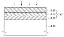
도 1을 참조하면, 반도체 기판(100) 상에 1차 유전체층(105)을 형성한다. 터널링층은 산화막의 단일막으로 형성된 구조에서, 유전체층 및 고유전상수(high-k) 물질을 포함하는 다층 구조로 변화하고 있다. 1차 유전체층(105)은 이후 다층 구조의 터널링층이 된다. 1차 유전체층(105)은 열산화(thermal oxidation) 방법 또는 라디칼 산화(radical oxidation) 방법을 이용하여 10Å 내지 30Å의 두께로 형성한다.Referring to FIG. 1, a primary
도 2를 참조하면, 1차 유전체층(105) 위에 고유전상수(high-k) 물질을 포함 하는 2차 유전체층(110)을 형성한다. 1차 유전체층(105) 위에 형성된 2차 유전체층(110)은 고유전상수 물질인 AlO, HfO, ZrO, HfSiO, HfSiON, HfAlO 및 HfAlON으로 이루어진 그룹에서 하나 이상의 물질을 선택하여 형성할 수 있다. 여기서 2차 유전체층(110)은 10Å 내지 100Å의 두께로 형성한다.Referring to FIG. 2, a secondary
도 3을 참조하면, 고유전상수 물질을 포함하는 2차 유전체층(110) 위에 질화물계 버퍼층(115)을 형성한다. 여기서 질화물계 버퍼층(115)은 실리콘나이트라이드(SiN)막을 10Å 내지 40Å의 두께로 형성한다.Referring to FIG. 3, the
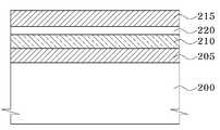
상술한 바와 같이, 터널링층은 산화막의 단일막으로 형성된 구조에서, 고유전상수(high-k) 물질을 포함하는 다층 구조, 예를 들어 삼중막 구조로 변화하고 있다. 도 8을 참조하면, 터널링층을 삼중막 구조로 형성하는 경우, 고유전상수물질막(210) 위에 산화막(215)을 형성하고 있다. 여기서 산화막(215)은 화학기상증착(CVD; Chemical vapor deposition)방법 또는 물리기상증착(PVD; Physical vapor deposition) 방법으로 형성한다. 그러나 도 8을 참조하면, 고유전상수물질막(210) 위에 화학기상증착방법 또는 물리기상증착방법을 이용하여 산화막(215)을 형성하면, 고유전상수물질막(210)과 산화막(215) 사이의 화학 반응에 의해 실리사이드(silicide)막 또는 실리케이트(silicate)막과 같은 계면막(interfacial layer, 220)이 형성된다. 이와 같이 고유전상수물질막(210)과 산화막(215) 사이에 계면막(220)이 형성되면 다층 구조로 이루어진 터널링층의 용량성 등가 두께(CET; Capacitance Equivalent Thickness)가 증가하는 문제가 발생하게 된다. 또한, 계면막(220)이 형성되면서 고유전상수물질막(210)과 산화막(215) 사이의 표면 거칠 기(roughness)도 증가할 뿐만 아니라, 전하 트랩(chrge trap)을 유발시켜 소자의 전기적 특성을 열화시키는 문제가 발생한다.As described above, the tunneling layer is changing from a structure formed of a single film of an oxide film to a multilayer structure including a high-k material, for example, a triple film structure. Referring to FIG. 8, when the tunneling layer is formed in a triple layer structure, an
이에 따라 고유전상수물질막(210)과 산화막(215) 사이에 계면막(220)이 형성되는 것을 방지하기 위해 본 발명의 실시예에서는, 고유전상수 물질을 포함하는 2차 유전체층(110) 위에 질화물계 버퍼층(115)을 형성한다. 질화물계 버퍼층(115)으로 실리콘 나이트라이드막을 형성하면 고유전상수 물질을 포함하는 2차 유전체층(110)과의 반응 작용이 억제되어 계면막이 형성되는 것을 방지할 수 있다.Accordingly, in order to prevent the
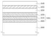
도 4를 참조하면, 질화물계 버퍼층(115) 상에 산화 처리를 진행하여 질화물계 버퍼층(115)을 실리콘옥사이드(SiO2)막(120)으로 변환한다. 본 발명의 실시예에서 진행하는 산화 처리는 통상의 열처리 대신에 인시츄 스팀 생성(ISSG; In-Situ Steam Generation) 산화방법을 이용한다. 인시츄 스팀 생성(ISSG) 산화방법은, 질화물계 버퍼층(115)이 형성된 반도체 기판(100)을 열처리 챔버 내에 로딩시킨 다음, 열처리 챔버 내에 수소(H2) 함유 가스 및 산소(O2) 함유 가스를 공급하여 라디컬 산화 반응을 유도하는 방법이다. 인시츄 스팀 생성(ISSG) 산화방법의 메커니즘(mechanism)은 수소와 산소를 연소할 때에 발생되는 라디칼 산화종(radical oxidation species)에 의한 산화이다. 일반적인 열처리, 예컨대 급속열처리(RTP; Rapid thermal process)에 의한 산화처리는 원자상 산화(on-atom oxidation)이다. 원자상 산화는 원자상에 활성 산화종이 직접 참여하여 산화되기 때문이다. 인시츄 스팀 생성(ISSG) 산화방법은 열처리 챔버 내에 수소(H2) 함유 가스 및 산소(O2) 함 유 가스를 공급하여 질화물계 버퍼층(115)과 열처리 챔버 내에서 반응하여 발생된 증기로 반응이 진행된다. 이때, 인시츄 스팀 생성(ISSG) 산화방법은 질화물 상에도 산화물을 성장시키는 특징이 있다. 이에 따라 인시츄 스팀 생성(ISSG) 산화방법으로 실리콘 나이트라이드막의 질소(nitrogen)와 산소(oxygen)를 치환시킴으로써 질화물계 버퍼층(115)은 실리콘옥사이드(SiO2)막을 포함하는 3차 유전체층(120)으로 변환된다. 이에 따라 반도체 기판(100) 상에는 1차 유전체층(105), 고유전상수 물질을 포함하는 2차 유전체층(110) 및 3차 유전체층(120)의 삼중막 구조의 터널링층(125)이 형성된다.Referring to FIG. 4, an oxidation process is performed on the
도 5를 참조하면, 터널링층(125) 위에 전하 트랩층(130)을 형성한다. 전하 트랩층(130)은 터널링층(125)을 관통하여 주입된 전자 또는 홀들을 트랩(trap)하는 층으로, 에너지 레벨이 균일하고 트랩 사이트가 많을수록 전하의 트랩이 잘 이루어져 소자의 프로그램 및 소거 속도가 증가한다. 여기서 전하 트랩층(130)은 실리콘 나이트라이드막을 10Å 내지 40Å의 두께로 형성할 수 있다.Referring to FIG. 5, the
도 6을 참조하면, 전하 트랩층(130) 위에 고유전율을 갖는 물질을 증착하여 차폐층(135)을 형성한다. 계속해서 차폐층(135) 위에 컨트롤게이트전극(140)을 형성한다. 여기서 차폐층(135)은 전하 트랩층(130)으로부터 컨트롤게이트전극(140) 쪽으로 전하가 이동하는 것을 차단하는 역할을 한다. 컨트롤게이트전극(140)은 반도체 기판(100)의 채널영역으로부터 전자들이나 홀들이 전하 트랩층(130) 내의 트랩 사이트로 트랩되도록 일정한 크기의 바이어스를 인가하는 역할을 한다. 이때 도 면에 비록 도시하지는 않았지만, 게이트 전극의 비저항을 낮추기 위해 컨트롤게이트전극(140) 위에 저저항층을 형성할 수도 있다.Referring to FIG. 6, a
도 7을 참조하면, 컨트롤게이트전극(140), 차폐층(135), 전하 트랩층(130) 및 터널링층(125)을 패터닝하여 게이트 스택(180)을 형성한다. 구체적으로, 컨트롤게이트전극(140) 위에 게이트 스택 형성영역을 설정하는 마스크막 패턴(미도시함)을 형성한다. 다음에 이 마스크막 패턴을 마스크로 한 식각 공정을 진행하여 게이트 스택(180)을 형성한다. 여기서 게이트 스택(180)은 터널링층 패턴(175), 전하트랩층 패턴(155), 차폐층 패턴(150) 및 컨트롤게이트전극 패턴(145)을 포함하여 이루어진다. 이때, 터널링층 패턴(175)은 1차 유전체층 패턴(170), 2차 유전체층 패턴(165) 및 3차 유전체층 패턴(160)이 적층된 구조로 이루어진다.Referring to FIG. 7, the
본 발명의 실시예에 따른 전하 트랩층을 갖는 불휘발성 메모리소자의 제조방법은, 터널링층을 산화막/고유전상수물질막/산화막의 삼중막 구조로 형성하는 경우, 고유전상수물질막 위에 실리콘 나이트라이드막을 형성하고, ISSG 산화방법을 이용하여 실리콘 나이트라이드막을 산화막으로 치환함으로써 고유전상수물질막과 산화막 사이에 계면막이 형성되는 것을 방지할 수 있다. 이에 따라 계면막에 의해 유발되는 터널링층의 용량성 등가 두께(CET) 증가, 전하 트랩 효과, 데이터 보유 특성 열화 및 불휘발성 메모리소자의 프로그램 및 소거 특성이 열화되는 문제를 방지할 수 있다.In the method of manufacturing a nonvolatile memory device having a charge trap layer according to an embodiment of the present invention, when the tunneling layer is formed of a triple layer structure of an oxide film, a high dielectric constant material film, and an oxide film, a silicon nitride film is formed on the high dielectric constant material film. The silicon nitride film is replaced with the oxide film using the ISSG oxidation method to prevent the formation of an interface film between the high dielectric constant material film and the oxide film. As a result, the capacitive equivalent thickness (CET) of the tunneling layer caused by the interfacial layer, the charge trap effect, the deterioration of data retention characteristics, and the program and erase characteristics of the nonvolatile memory device can be prevented.
도 1 내지 도 7은 본 발명의 실시예에 따른 전하 트랩층을 갖는 불휘발성 메모리소자의 제조방법을 설명하기 위해 나타내보인 도면들이다.1 to 7 illustrate a method of manufacturing a nonvolatile memory device having a charge trap layer according to an embodiment of the present invention.
도 8은 터널링층을 다층 구조로 형성하는 경우 발생된 문제점을 설명하기 위해 나타내보인 도면이다.FIG. 8 is a diagram illustrating a problem caused when the tunneling layer is formed in a multilayer structure.
Claims (5)
Translated fromKoreanPriority Applications (2)
| Application Number | Priority Date | Filing Date | Title |
|---|---|---|---|
| KR1020080020700AKR100950477B1 (en) | 2008-03-05 | 2008-03-05 | Method for manufacturing nonvolatile memory device having charge trap layer |
| US12/347,289US7736975B2 (en) | 2008-03-05 | 2008-12-31 | Method for manufacturing non-volatile memory device having charge trap layer |
Applications Claiming Priority (1)
| Application Number | Priority Date | Filing Date | Title |
|---|---|---|---|
| KR1020080020700AKR100950477B1 (en) | 2008-03-05 | 2008-03-05 | Method for manufacturing nonvolatile memory device having charge trap layer |
Publications (2)
| Publication Number | Publication Date |
|---|---|
| KR20090095393A KR20090095393A (en) | 2009-09-09 |
| KR100950477B1true KR100950477B1 (en) | 2010-03-31 |
Family
ID=41054071
Family Applications (1)
| Application Number | Title | Priority Date | Filing Date |
|---|---|---|---|
| KR1020080020700AExpired - Fee RelatedKR100950477B1 (en) | 2008-03-05 | 2008-03-05 | Method for manufacturing nonvolatile memory device having charge trap layer |
Country Status (2)
| Country | Link |
|---|---|
| US (1) | US7736975B2 (en) |
| KR (1) | KR100950477B1 (en) |
Families Citing this family (15)
| Publication number | Priority date | Publication date | Assignee | Title |
|---|---|---|---|---|
| US8633537B2 (en) | 2007-05-25 | 2014-01-21 | Cypress Semiconductor Corporation | Memory transistor with multiple charge storing layers and a high work function gate electrode |
| US8614124B2 (en) | 2007-05-25 | 2013-12-24 | Cypress Semiconductor Corporation | SONOS ONO stack scaling |
| US8940645B2 (en) | 2007-05-25 | 2015-01-27 | Cypress Semiconductor Corporation | Radical oxidation process for fabricating a nonvolatile charge trap memory device |
| US9449831B2 (en) | 2007-05-25 | 2016-09-20 | Cypress Semiconductor Corporation | Oxide-nitride-oxide stack having multiple oxynitride layers |
| US20090179253A1 (en) | 2007-05-25 | 2009-07-16 | Cypress Semiconductor Corporation | Oxide-nitride-oxide stack having multiple oxynitride layers |
| US9299568B2 (en) | 2007-05-25 | 2016-03-29 | Cypress Semiconductor Corporation | SONOS ONO stack scaling |
| US9431549B2 (en) | 2007-12-12 | 2016-08-30 | Cypress Semiconductor Corporation | Nonvolatile charge trap memory device having a high dielectric constant blocking region |
| US8222688B1 (en) | 2009-04-24 | 2012-07-17 | Cypress Semiconductor Corporation | SONOS stack with split nitride memory layer |
| US8710578B2 (en) | 2009-04-24 | 2014-04-29 | Cypress Semiconductor Corporation | SONOS stack with split nitride memory layer |
| US20110101442A1 (en)* | 2009-11-02 | 2011-05-05 | Applied Materials, Inc. | Multi-Layer Charge Trap Silicon Nitride/Oxynitride Layer Engineering with Interface Region Control |
| CN102446963A (en)* | 2010-10-15 | 2012-05-09 | 中芯国际集成电路制造(上海)有限公司 | Composite tunneling dielectric layer, manufacturing method thereof and nonvolatile memory |
| US8685813B2 (en) | 2012-02-15 | 2014-04-01 | Cypress Semiconductor Corporation | Method of integrating a charge-trapping gate stack into a CMOS flow |
| US10622449B2 (en) | 2012-04-05 | 2020-04-14 | X-Fab Semiconductor Foundries Gmbh | Method of fabricating a tunnel oxide layer and a tunnel oxide layer for a semiconductor device |
| US9627213B2 (en)* | 2012-04-05 | 2017-04-18 | X-Fab Semiconductor Foundries Ag | Method of fabricating a tunnel oxide layer and a tunnel oxide layer for a semiconductor device |
| KR20150062768A (en)* | 2013-11-29 | 2015-06-08 | 삼성전자주식회사 | Methods of Fabricating Semiconductor devices having Double-Layered Blocking Insulating Layers |
Citations (4)
| Publication number | Priority date | Publication date | Assignee | Title |
|---|---|---|---|---|
| KR100587670B1 (en) | 2004-01-08 | 2006-06-08 | 삼성전자주식회사 | Dielectric film formation method of nonvolatile memory cell |
| KR100684900B1 (en) | 2005-04-12 | 2007-02-20 | 삼성전자주식회사 | Nonvolatile Memory Device and Its Operation Method |
| KR20080069919A (en)* | 2007-01-24 | 2008-07-29 | 가부시끼가이샤 도시바 | Semiconductor Memory and Manufacturing Method Thereof |
| KR100886532B1 (en) | 2001-06-25 | 2009-03-02 | 엑손모빌 케미칼 패턴츠 인코포레이티드 | Molecular sieve catalyst compositions, their preparation and their use in the process of conversion |
Family Cites Families (3)
| Publication number | Priority date | Publication date | Assignee | Title |
|---|---|---|---|---|
| JP4987206B2 (en) | 2000-03-13 | 2012-07-25 | 公益財団法人国際科学振興財団 | Method for manufacturing flash memory device |
| US7405125B2 (en) | 2004-06-01 | 2008-07-29 | Macronix International Co., Ltd. | Tunnel oxynitride in flash memories |
| KR101003492B1 (en)* | 2007-12-21 | 2010-12-30 | 주식회사 하이닉스반도체 | Method of forming a nonvolatile memory device having a charge trap layer |
- 2008
- 2008-03-05KRKR1020080020700Apatent/KR100950477B1/ennot_activeExpired - Fee Related
- 2008-12-31USUS12/347,289patent/US7736975B2/ennot_activeExpired - Fee Related
Patent Citations (4)
| Publication number | Priority date | Publication date | Assignee | Title |
|---|---|---|---|---|
| KR100886532B1 (en) | 2001-06-25 | 2009-03-02 | 엑손모빌 케미칼 패턴츠 인코포레이티드 | Molecular sieve catalyst compositions, their preparation and their use in the process of conversion |
| KR100587670B1 (en) | 2004-01-08 | 2006-06-08 | 삼성전자주식회사 | Dielectric film formation method of nonvolatile memory cell |
| KR100684900B1 (en) | 2005-04-12 | 2007-02-20 | 삼성전자주식회사 | Nonvolatile Memory Device and Its Operation Method |
| KR20080069919A (en)* | 2007-01-24 | 2008-07-29 | 가부시끼가이샤 도시바 | Semiconductor Memory and Manufacturing Method Thereof |
Also Published As
| Publication number | Publication date |
|---|---|
| US20090227116A1 (en) | 2009-09-10 |
| KR20090095393A (en) | 2009-09-09 |
| US7736975B2 (en) | 2010-06-15 |
Similar Documents
| Publication | Publication Date | Title |
|---|---|---|
| KR100950477B1 (en) | Method for manufacturing nonvolatile memory device having charge trap layer | |
| KR100890040B1 (en) | Nonvolatile memory device having a charge trap layer and method of manufacturing same | |
| KR101033221B1 (en) | Nonvolatile memory device having a charge trap layer and method of manufacturing same | |
| US7981786B2 (en) | Method of fabricating non-volatile memory device having charge trapping layer | |
| US20080272424A1 (en) | Nonvolatile Memory Device Having Fast Erase Speed And Improved Retention Characteristics And Method For Fabricating The Same | |
| US8044454B2 (en) | Non-volatile memory device | |
| US7795159B2 (en) | Charge trap layer for a charge trap semiconductor memory device and method of manufacturing the same | |
| KR101410429B1 (en) | Non-volatile memory device and methods of forming the same | |
| KR101153310B1 (en) | Method for manufacturing a mos semiconductor memory device, and plasma cvd device | |
| KR100886352B1 (en) | Nonvolatile Memory Device and Manufacturing Method Thereof | |
| US7919371B2 (en) | Method for fabricating non-volatile memory device with charge trapping layer | |
| KR100950478B1 (en) | Method for manufacturing nonvolatile memory device having charge trap layer | |
| KR100811272B1 (en) | Nonvolatile memory device having a charge trap layer and method of manufacturing same | |
| KR20070062013A (en) | Dielectric Film Formation Method of Flash Memory Device | |
| KR20070106155A (en) | Manufacturing method of nonvolatile memory device | |
| KR100685742B1 (en) | Nonvolatile Memory Device and Manufacturing Method Thereof | |
| KR100641074B1 (en) | Charge trap type nonvolatile memory device and manufacturing method thereof | |
| KR20090097497A (en) | Method of forming nonvolatile memory device | |
| KR20080010514A (en) | Method of forming an insulating film structure and method of forming a nonvolatile memory device using the same | |
| KR100933840B1 (en) | Manufacturing Method of Flash Memory Device | |
| KR100833445B1 (en) | Manufacturing Method of Flash Memory Device | |
| KR20090086874A (en) | Method of forming a nonvolatile memory device having a charge trap layer | |
| KR20090020982A (en) | Method of forming a semiconductor device | |
| KR20080029656A (en) | Gate dielectric and manufacturing method thereof | |
| KR20090068001A (en) | Nonvolatile memory device having a charge trap layer and method of manufacturing same |
Legal Events
| Date | Code | Title | Description |
|---|---|---|---|
| A201 | Request for examination | ||
| PA0109 | Patent application | St.27 status event code:A-0-1-A10-A12-nap-PA0109 | |
| PA0201 | Request for examination | St.27 status event code:A-1-2-D10-D11-exm-PA0201 | |
| D13-X000 | Search requested | St.27 status event code:A-1-2-D10-D13-srh-X000 | |
| D14-X000 | Search report completed | St.27 status event code:A-1-2-D10-D14-srh-X000 | |
| PG1501 | Laying open of application | St.27 status event code:A-1-1-Q10-Q12-nap-PG1501 | |
| E902 | Notification of reason for refusal | ||
| PE0902 | Notice of grounds for rejection | St.27 status event code:A-1-2-D10-D21-exm-PE0902 | |
| P11-X000 | Amendment of application requested | St.27 status event code:A-2-2-P10-P11-nap-X000 | |
| P13-X000 | Application amended | St.27 status event code:A-2-2-P10-P13-nap-X000 | |
| E701 | Decision to grant or registration of patent right | ||
| PE0701 | Decision of registration | St.27 status event code:A-1-2-D10-D22-exm-PE0701 | |
| GRNT | Written decision to grant | ||
| PR0701 | Registration of establishment | St.27 status event code:A-2-4-F10-F11-exm-PR0701 | |
| PR1002 | Payment of registration fee | St.27 status event code:A-2-2-U10-U11-oth-PR1002 Fee payment year number:1 | |
| PG1601 | Publication of registration | St.27 status event code:A-4-4-Q10-Q13-nap-PG1601 | |
| PN2301 | Change of applicant | St.27 status event code:A-5-5-R10-R13-asn-PN2301 St.27 status event code:A-5-5-R10-R11-asn-PN2301 | |
| PN2301 | Change of applicant | St.27 status event code:A-5-5-R10-R13-asn-PN2301 St.27 status event code:A-5-5-R10-R11-asn-PN2301 | |
| LAPS | Lapse due to unpaid annual fee | ||
| PC1903 | Unpaid annual fee | St.27 status event code:A-4-4-U10-U13-oth-PC1903 Not in force date:20130325 Payment event data comment text:Termination Category : DEFAULT_OF_REGISTRATION_FEE | |
| PC1903 | Unpaid annual fee | St.27 status event code:N-4-6-H10-H13-oth-PC1903 Ip right cessation event data comment text:Termination Category : DEFAULT_OF_REGISTRATION_FEE Not in force date:20130325 | |
| PN2301 | Change of applicant | St.27 status event code:A-5-5-R10-R13-asn-PN2301 St.27 status event code:A-5-5-R10-R11-asn-PN2301 | |
| P22-X000 | Classification modified | St.27 status event code:A-4-4-P10-P22-nap-X000 | |
| P22-X000 | Classification modified | St.27 status event code:A-4-4-P10-P22-nap-X000 |