KR100945800B1 - Method for manufacturing heterogeneous bonded wafer - Google Patents
Method for manufacturing heterogeneous bonded waferDownload PDFInfo
- Publication number
- KR100945800B1 KR100945800B1KR1020090050859AKR20090050859AKR100945800B1KR 100945800 B1KR100945800 B1KR 100945800B1KR 1020090050859 AKR1020090050859 AKR 1020090050859AKR 20090050859 AKR20090050859 AKR 20090050859AKR 100945800 B1KR100945800 B1KR 100945800B1
- Authority
- KR
- South Korea
- Prior art keywords
- wafer
- bonding
- heterojunction
- manufacturing
- electrical connection
- Prior art date
- Legal status (The legal status is an assumption and is not a legal conclusion. Google has not performed a legal analysis and makes no representation as to the accuracy of the status listed.)
- Expired - Fee Related
Links
Images


Classifications
- H—ELECTRICITY
- H01—ELECTRIC ELEMENTS
- H01L—SEMICONDUCTOR DEVICES NOT COVERED BY CLASS H10
- H01L21/00—Processes or apparatus adapted for the manufacture or treatment of semiconductor or solid state devices or of parts thereof
- H01L21/02—Manufacture or treatment of semiconductor devices or of parts thereof
- H01L21/04—Manufacture or treatment of semiconductor devices or of parts thereof the devices having potential barriers, e.g. a PN junction, depletion layer or carrier concentration layer
- H01L21/18—Manufacture or treatment of semiconductor devices or of parts thereof the devices having potential barriers, e.g. a PN junction, depletion layer or carrier concentration layer the devices having semiconductor bodies comprising elements of Group IV of the Periodic Table or AIIIBV compounds with or without impurities, e.g. doping materials
- H01L21/185—Joining of semiconductor bodies for junction formation
- H01L21/187—Joining of semiconductor bodies for junction formation by direct bonding
- H—ELECTRICITY
- H01—ELECTRIC ELEMENTS
- H01L—SEMICONDUCTOR DEVICES NOT COVERED BY CLASS H10
- H01L21/00—Processes or apparatus adapted for the manufacture or treatment of semiconductor or solid state devices or of parts thereof
- H01L21/02—Manufacture or treatment of semiconductor devices or of parts thereof
- H01L21/04—Manufacture or treatment of semiconductor devices or of parts thereof the devices having potential barriers, e.g. a PN junction, depletion layer or carrier concentration layer
- H01L21/18—Manufacture or treatment of semiconductor devices or of parts thereof the devices having potential barriers, e.g. a PN junction, depletion layer or carrier concentration layer the devices having semiconductor bodies comprising elements of Group IV of the Periodic Table or AIIIBV compounds with or without impurities, e.g. doping materials
- H01L21/20—Deposition of semiconductor materials on a substrate, e.g. epitaxial growth solid phase epitaxy
- H—ELECTRICITY
- H01—ELECTRIC ELEMENTS
- H01L—SEMICONDUCTOR DEVICES NOT COVERED BY CLASS H10
- H01L23/00—Details of semiconductor or other solid state devices
- H01L23/58—Structural electrical arrangements for semiconductor devices not otherwise provided for, e.g. in combination with batteries
- H01L23/585—Structural electrical arrangements for semiconductor devices not otherwise provided for, e.g. in combination with batteries comprising conductive layers or plates or strips or rods or rings
- H—ELECTRICITY
- H01—ELECTRIC ELEMENTS
- H01L—SEMICONDUCTOR DEVICES NOT COVERED BY CLASS H10
- H01L24/00—Arrangements for connecting or disconnecting semiconductor or solid-state bodies; Methods or apparatus related thereto
- H01L24/01—Means for bonding being attached to, or being formed on, the surface to be connected, e.g. chip-to-package, die-attach, "first-level" interconnects; Manufacturing methods related thereto
- H01L24/26—Layer connectors, e.g. plate connectors, solder or adhesive layers; Manufacturing methods related thereto
- H01L24/28—Structure, shape, material or disposition of the layer connectors prior to the connecting process
- H01L24/29—Structure, shape, material or disposition of the layer connectors prior to the connecting process of an individual layer connector
- H—ELECTRICITY
- H01—ELECTRIC ELEMENTS
- H01L—SEMICONDUCTOR DEVICES NOT COVERED BY CLASS H10
- H01L24/00—Arrangements for connecting or disconnecting semiconductor or solid-state bodies; Methods or apparatus related thereto
- H01L24/01—Means for bonding being attached to, or being formed on, the surface to be connected, e.g. chip-to-package, die-attach, "first-level" interconnects; Manufacturing methods related thereto
- H01L24/26—Layer connectors, e.g. plate connectors, solder or adhesive layers; Manufacturing methods related thereto
- H01L24/28—Structure, shape, material or disposition of the layer connectors prior to the connecting process
- H01L24/30—Structure, shape, material or disposition of the layer connectors prior to the connecting process of a plurality of layer connectors
- H—ELECTRICITY
- H01—ELECTRIC ELEMENTS
- H01L—SEMICONDUCTOR DEVICES NOT COVERED BY CLASS H10
- H01L24/00—Arrangements for connecting or disconnecting semiconductor or solid-state bodies; Methods or apparatus related thereto
- H01L24/73—Means for bonding being of different types provided for in two or more of groups H01L24/10, H01L24/18, H01L24/26, H01L24/34, H01L24/42, H01L24/50, H01L24/63, H01L24/71
- H—ELECTRICITY
- H01—ELECTRIC ELEMENTS
- H01L—SEMICONDUCTOR DEVICES NOT COVERED BY CLASS H10
- H01L24/00—Arrangements for connecting or disconnecting semiconductor or solid-state bodies; Methods or apparatus related thereto
- H01L24/91—Methods for connecting semiconductor or solid state bodies including different methods provided for in two or more of groups H01L24/80 - H01L24/90
- H01L24/92—Specific sequence of method steps
- H—ELECTRICITY
- H01—ELECTRIC ELEMENTS
- H01L—SEMICONDUCTOR DEVICES NOT COVERED BY CLASS H10
- H01L24/00—Arrangements for connecting or disconnecting semiconductor or solid-state bodies; Methods or apparatus related thereto
- H01L24/93—Batch processes
- H01L24/94—Batch processes at wafer-level, i.e. with connecting carried out on a wafer comprising a plurality of undiced individual devices
- H—ELECTRICITY
- H01—ELECTRIC ELEMENTS
- H01L—SEMICONDUCTOR DEVICES NOT COVERED BY CLASS H10
- H01L25/00—Assemblies consisting of a plurality of semiconductor or other solid state devices
- H01L25/03—Assemblies consisting of a plurality of semiconductor or other solid state devices all the devices being of a type provided for in a single subclass of subclasses H10B, H10D, H10F, H10H, H10K or H10N, e.g. assemblies of rectifier diodes
- H01L25/04—Assemblies consisting of a plurality of semiconductor or other solid state devices all the devices being of a type provided for in a single subclass of subclasses H10B, H10D, H10F, H10H, H10K or H10N, e.g. assemblies of rectifier diodes the devices not having separate containers
- H01L25/065—Assemblies consisting of a plurality of semiconductor or other solid state devices all the devices being of a type provided for in a single subclass of subclasses H10B, H10D, H10F, H10H, H10K or H10N, e.g. assemblies of rectifier diodes the devices not having separate containers the devices being of a type provided for in group H10D89/00
- H01L25/0657—Stacked arrangements of devices
- H—ELECTRICITY
- H01—ELECTRIC ELEMENTS
- H01L—SEMICONDUCTOR DEVICES NOT COVERED BY CLASS H10
- H01L25/00—Assemblies consisting of a plurality of semiconductor or other solid state devices
- H01L25/50—Multistep manufacturing processes of assemblies consisting of devices, the devices being individual devices of subclass H10D or integrated devices of class H10
- H—ELECTRICITY
- H01—ELECTRIC ELEMENTS
- H01L—SEMICONDUCTOR DEVICES NOT COVERED BY CLASS H10
- H01L21/00—Processes or apparatus adapted for the manufacture or treatment of semiconductor or solid state devices or of parts thereof
- H01L21/70—Manufacture or treatment of devices consisting of a plurality of solid state components formed in or on a common substrate or of parts thereof; Manufacture of integrated circuit devices or of parts thereof
- H01L21/71—Manufacture of specific parts of devices defined in group H01L21/70
- H01L21/768—Applying interconnections to be used for carrying current between separate components within a device comprising conductors and dielectrics
- H01L21/76898—Applying interconnections to be used for carrying current between separate components within a device comprising conductors and dielectrics formed through a semiconductor substrate
- H—ELECTRICITY
- H01—ELECTRIC ELEMENTS
- H01L—SEMICONDUCTOR DEVICES NOT COVERED BY CLASS H10
- H01L2224/00—Indexing scheme for arrangements for connecting or disconnecting semiconductor or solid-state bodies and methods related thereto as covered by H01L24/00
- H01L2224/01—Means for bonding being attached to, or being formed on, the surface to be connected, e.g. chip-to-package, die-attach, "first-level" interconnects; Manufacturing methods related thereto
- H01L2224/02—Bonding areas; Manufacturing methods related thereto
- H01L2224/04—Structure, shape, material or disposition of the bonding areas prior to the connecting process
- H01L2224/05—Structure, shape, material or disposition of the bonding areas prior to the connecting process of an individual bonding area
- H01L2224/0554—External layer
- H01L2224/0556—Disposition
- H01L2224/05568—Disposition the whole external layer protruding from the surface
- H—ELECTRICITY
- H01—ELECTRIC ELEMENTS
- H01L—SEMICONDUCTOR DEVICES NOT COVERED BY CLASS H10
- H01L2224/00—Indexing scheme for arrangements for connecting or disconnecting semiconductor or solid-state bodies and methods related thereto as covered by H01L24/00
- H01L2224/01—Means for bonding being attached to, or being formed on, the surface to be connected, e.g. chip-to-package, die-attach, "first-level" interconnects; Manufacturing methods related thereto
- H01L2224/02—Bonding areas; Manufacturing methods related thereto
- H01L2224/04—Structure, shape, material or disposition of the bonding areas prior to the connecting process
- H01L2224/05—Structure, shape, material or disposition of the bonding areas prior to the connecting process of an individual bonding area
- H01L2224/0554—External layer
- H01L2224/05573—Single external layer
- H—ELECTRICITY
- H01—ELECTRIC ELEMENTS
- H01L—SEMICONDUCTOR DEVICES NOT COVERED BY CLASS H10
- H01L2224/00—Indexing scheme for arrangements for connecting or disconnecting semiconductor or solid-state bodies and methods related thereto as covered by H01L24/00
- H01L2224/01—Means for bonding being attached to, or being formed on, the surface to be connected, e.g. chip-to-package, die-attach, "first-level" interconnects; Manufacturing methods related thereto
- H01L2224/02—Bonding areas; Manufacturing methods related thereto
- H01L2224/04—Structure, shape, material or disposition of the bonding areas prior to the connecting process
- H01L2224/05—Structure, shape, material or disposition of the bonding areas prior to the connecting process of an individual bonding area
- H01L2224/0554—External layer
- H01L2224/05599—Material
- H01L2224/056—Material with a principal constituent of the material being a metal or a metalloid, e.g. boron [B], silicon [Si], germanium [Ge], arsenic [As], antimony [Sb], tellurium [Te] and polonium [Po], and alloys thereof
- H01L2224/05601—Material with a principal constituent of the material being a metal or a metalloid, e.g. boron [B], silicon [Si], germanium [Ge], arsenic [As], antimony [Sb], tellurium [Te] and polonium [Po], and alloys thereof the principal constituent melting at a temperature of less than 400°C
- H01L2224/05611—Tin [Sn] as principal constituent
- H—ELECTRICITY
- H01—ELECTRIC ELEMENTS
- H01L—SEMICONDUCTOR DEVICES NOT COVERED BY CLASS H10
- H01L2224/00—Indexing scheme for arrangements for connecting or disconnecting semiconductor or solid-state bodies and methods related thereto as covered by H01L24/00
- H01L2224/01—Means for bonding being attached to, or being formed on, the surface to be connected, e.g. chip-to-package, die-attach, "first-level" interconnects; Manufacturing methods related thereto
- H01L2224/02—Bonding areas; Manufacturing methods related thereto
- H01L2224/04—Structure, shape, material or disposition of the bonding areas prior to the connecting process
- H01L2224/05—Structure, shape, material or disposition of the bonding areas prior to the connecting process of an individual bonding area
- H01L2224/0554—External layer
- H01L2224/05599—Material
- H01L2224/056—Material with a principal constituent of the material being a metal or a metalloid, e.g. boron [B], silicon [Si], germanium [Ge], arsenic [As], antimony [Sb], tellurium [Te] and polonium [Po], and alloys thereof
- H01L2224/05617—Material with a principal constituent of the material being a metal or a metalloid, e.g. boron [B], silicon [Si], germanium [Ge], arsenic [As], antimony [Sb], tellurium [Te] and polonium [Po], and alloys thereof the principal constituent melting at a temperature of greater than or equal to 400°C and less than 950°C
- H01L2224/05624—Aluminium [Al] as principal constituent
- H—ELECTRICITY
- H01—ELECTRIC ELEMENTS
- H01L—SEMICONDUCTOR DEVICES NOT COVERED BY CLASS H10
- H01L2224/00—Indexing scheme for arrangements for connecting or disconnecting semiconductor or solid-state bodies and methods related thereto as covered by H01L24/00
- H01L2224/01—Means for bonding being attached to, or being formed on, the surface to be connected, e.g. chip-to-package, die-attach, "first-level" interconnects; Manufacturing methods related thereto
- H01L2224/02—Bonding areas; Manufacturing methods related thereto
- H01L2224/04—Structure, shape, material or disposition of the bonding areas prior to the connecting process
- H01L2224/05—Structure, shape, material or disposition of the bonding areas prior to the connecting process of an individual bonding area
- H01L2224/0554—External layer
- H01L2224/05599—Material
- H01L2224/056—Material with a principal constituent of the material being a metal or a metalloid, e.g. boron [B], silicon [Si], germanium [Ge], arsenic [As], antimony [Sb], tellurium [Te] and polonium [Po], and alloys thereof
- H01L2224/05638—Material with a principal constituent of the material being a metal or a metalloid, e.g. boron [B], silicon [Si], germanium [Ge], arsenic [As], antimony [Sb], tellurium [Te] and polonium [Po], and alloys thereof the principal constituent melting at a temperature of greater than or equal to 950°C and less than 1550°C
- H01L2224/05644—Gold [Au] as principal constituent
- H—ELECTRICITY
- H01—ELECTRIC ELEMENTS
- H01L—SEMICONDUCTOR DEVICES NOT COVERED BY CLASS H10
- H01L2224/00—Indexing scheme for arrangements for connecting or disconnecting semiconductor or solid-state bodies and methods related thereto as covered by H01L24/00
- H01L2224/01—Means for bonding being attached to, or being formed on, the surface to be connected, e.g. chip-to-package, die-attach, "first-level" interconnects; Manufacturing methods related thereto
- H01L2224/02—Bonding areas; Manufacturing methods related thereto
- H01L2224/04—Structure, shape, material or disposition of the bonding areas prior to the connecting process
- H01L2224/05—Structure, shape, material or disposition of the bonding areas prior to the connecting process of an individual bonding area
- H01L2224/0554—External layer
- H01L2224/05599—Material
- H01L2224/056—Material with a principal constituent of the material being a metal or a metalloid, e.g. boron [B], silicon [Si], germanium [Ge], arsenic [As], antimony [Sb], tellurium [Te] and polonium [Po], and alloys thereof
- H01L2224/05638—Material with a principal constituent of the material being a metal or a metalloid, e.g. boron [B], silicon [Si], germanium [Ge], arsenic [As], antimony [Sb], tellurium [Te] and polonium [Po], and alloys thereof the principal constituent melting at a temperature of greater than or equal to 950°C and less than 1550°C
- H01L2224/05647—Copper [Cu] as principal constituent
- H—ELECTRICITY
- H01—ELECTRIC ELEMENTS
- H01L—SEMICONDUCTOR DEVICES NOT COVERED BY CLASS H10
- H01L2224/00—Indexing scheme for arrangements for connecting or disconnecting semiconductor or solid-state bodies and methods related thereto as covered by H01L24/00
- H01L2224/01—Means for bonding being attached to, or being formed on, the surface to be connected, e.g. chip-to-package, die-attach, "first-level" interconnects; Manufacturing methods related thereto
- H01L2224/10—Bump connectors; Manufacturing methods related thereto
- H01L2224/15—Structure, shape, material or disposition of the bump connectors after the connecting process
- H01L2224/16—Structure, shape, material or disposition of the bump connectors after the connecting process of an individual bump connector
- H—ELECTRICITY
- H01—ELECTRIC ELEMENTS
- H01L—SEMICONDUCTOR DEVICES NOT COVERED BY CLASS H10
- H01L2224/00—Indexing scheme for arrangements for connecting or disconnecting semiconductor or solid-state bodies and methods related thereto as covered by H01L24/00
- H01L2224/01—Means for bonding being attached to, or being formed on, the surface to be connected, e.g. chip-to-package, die-attach, "first-level" interconnects; Manufacturing methods related thereto
- H01L2224/26—Layer connectors, e.g. plate connectors, solder or adhesive layers; Manufacturing methods related thereto
- H01L2224/28—Structure, shape, material or disposition of the layer connectors prior to the connecting process
- H01L2224/29—Structure, shape, material or disposition of the layer connectors prior to the connecting process of an individual layer connector
- H01L2224/29001—Core members of the layer connector
- H01L2224/29099—Material
- H01L2224/291—Material with a principal constituent of the material being a metal or a metalloid, e.g. boron [B], silicon [Si], germanium [Ge], arsenic [As], antimony [Sb], tellurium [Te] and polonium [Po], and alloys thereof
- H01L2224/29101—Material with a principal constituent of the material being a metal or a metalloid, e.g. boron [B], silicon [Si], germanium [Ge], arsenic [As], antimony [Sb], tellurium [Te] and polonium [Po], and alloys thereof the principal constituent melting at a temperature of less than 400°C
- H—ELECTRICITY
- H01—ELECTRIC ELEMENTS
- H01L—SEMICONDUCTOR DEVICES NOT COVERED BY CLASS H10
- H01L2224/00—Indexing scheme for arrangements for connecting or disconnecting semiconductor or solid-state bodies and methods related thereto as covered by H01L24/00
- H01L2224/01—Means for bonding being attached to, or being formed on, the surface to be connected, e.g. chip-to-package, die-attach, "first-level" interconnects; Manufacturing methods related thereto
- H01L2224/26—Layer connectors, e.g. plate connectors, solder or adhesive layers; Manufacturing methods related thereto
- H01L2224/28—Structure, shape, material or disposition of the layer connectors prior to the connecting process
- H01L2224/29—Structure, shape, material or disposition of the layer connectors prior to the connecting process of an individual layer connector
- H01L2224/29001—Core members of the layer connector
- H01L2224/29099—Material
- H01L2224/2919—Material with a principal constituent of the material being a polymer, e.g. polyester, phenolic based polymer, epoxy
- H—ELECTRICITY
- H01—ELECTRIC ELEMENTS
- H01L—SEMICONDUCTOR DEVICES NOT COVERED BY CLASS H10
- H01L2224/00—Indexing scheme for arrangements for connecting or disconnecting semiconductor or solid-state bodies and methods related thereto as covered by H01L24/00
- H01L2224/01—Means for bonding being attached to, or being formed on, the surface to be connected, e.g. chip-to-package, die-attach, "first-level" interconnects; Manufacturing methods related thereto
- H01L2224/26—Layer connectors, e.g. plate connectors, solder or adhesive layers; Manufacturing methods related thereto
- H01L2224/31—Structure, shape, material or disposition of the layer connectors after the connecting process
- H01L2224/32—Structure, shape, material or disposition of the layer connectors after the connecting process of an individual layer connector
- H01L2224/3201—Structure
- H01L2224/32012—Structure relative to the bonding area, e.g. bond pad
- H01L2224/32014—Structure relative to the bonding area, e.g. bond pad the layer connector being smaller than the bonding area, e.g. bond pad
- H—ELECTRICITY
- H01—ELECTRIC ELEMENTS
- H01L—SEMICONDUCTOR DEVICES NOT COVERED BY CLASS H10
- H01L2224/00—Indexing scheme for arrangements for connecting or disconnecting semiconductor or solid-state bodies and methods related thereto as covered by H01L24/00
- H01L2224/73—Means for bonding being of different types provided for in two or more of groups H01L2224/10, H01L2224/18, H01L2224/26, H01L2224/34, H01L2224/42, H01L2224/50, H01L2224/63, H01L2224/71
- H—ELECTRICITY
- H01—ELECTRIC ELEMENTS
- H01L—SEMICONDUCTOR DEVICES NOT COVERED BY CLASS H10
- H01L2224/00—Indexing scheme for arrangements for connecting or disconnecting semiconductor or solid-state bodies and methods related thereto as covered by H01L24/00
- H01L2224/80—Methods for connecting semiconductor or other solid state bodies using means for bonding being attached to, or being formed on, the surface to be connected
- H01L2224/81—Methods for connecting semiconductor or other solid state bodies using means for bonding being attached to, or being formed on, the surface to be connected using a bump connector
- H01L2224/8119—Arrangement of the bump connectors prior to mounting
- H01L2224/81193—Arrangement of the bump connectors prior to mounting wherein the bump connectors are disposed on both the semiconductor or solid-state body and another item or body to be connected to the semiconductor or solid-state body
- H—ELECTRICITY
- H01—ELECTRIC ELEMENTS
- H01L—SEMICONDUCTOR DEVICES NOT COVERED BY CLASS H10
- H01L2224/00—Indexing scheme for arrangements for connecting or disconnecting semiconductor or solid-state bodies and methods related thereto as covered by H01L24/00
- H01L2224/80—Methods for connecting semiconductor or other solid state bodies using means for bonding being attached to, or being formed on, the surface to be connected
- H01L2224/81—Methods for connecting semiconductor or other solid state bodies using means for bonding being attached to, or being formed on, the surface to be connected using a bump connector
- H01L2224/818—Bonding techniques
- H01L2224/81801—Soldering or alloying
- H—ELECTRICITY
- H01—ELECTRIC ELEMENTS
- H01L—SEMICONDUCTOR DEVICES NOT COVERED BY CLASS H10
- H01L2224/00—Indexing scheme for arrangements for connecting or disconnecting semiconductor or solid-state bodies and methods related thereto as covered by H01L24/00
- H01L2224/80—Methods for connecting semiconductor or other solid state bodies using means for bonding being attached to, or being formed on, the surface to be connected
- H01L2224/81—Methods for connecting semiconductor or other solid state bodies using means for bonding being attached to, or being formed on, the surface to be connected using a bump connector
- H01L2224/818—Bonding techniques
- H01L2224/81894—Direct bonding, i.e. joining surfaces by means of intermolecular attracting interactions at their interfaces, e.g. covalent bonds, van der Waals forces
- H—ELECTRICITY
- H01—ELECTRIC ELEMENTS
- H01L—SEMICONDUCTOR DEVICES NOT COVERED BY CLASS H10
- H01L2224/00—Indexing scheme for arrangements for connecting or disconnecting semiconductor or solid-state bodies and methods related thereto as covered by H01L24/00
- H01L2224/80—Methods for connecting semiconductor or other solid state bodies using means for bonding being attached to, or being formed on, the surface to be connected
- H01L2224/83—Methods for connecting semiconductor or other solid state bodies using means for bonding being attached to, or being formed on, the surface to be connected using a layer connector
- H01L2224/8319—Arrangement of the layer connectors prior to mounting
- H01L2224/83194—Lateral distribution of the layer connectors
- H—ELECTRICITY
- H01—ELECTRIC ELEMENTS
- H01L—SEMICONDUCTOR DEVICES NOT COVERED BY CLASS H10
- H01L2224/00—Indexing scheme for arrangements for connecting or disconnecting semiconductor or solid-state bodies and methods related thereto as covered by H01L24/00
- H01L2224/80—Methods for connecting semiconductor or other solid state bodies using means for bonding being attached to, or being formed on, the surface to be connected
- H01L2224/83—Methods for connecting semiconductor or other solid state bodies using means for bonding being attached to, or being formed on, the surface to be connected using a layer connector
- H01L2224/838—Bonding techniques
- H01L2224/83894—Direct bonding, i.e. joining surfaces by means of intermolecular attracting interactions at their interfaces, e.g. covalent bonds, van der Waals forces
- H—ELECTRICITY
- H01—ELECTRIC ELEMENTS
- H01L—SEMICONDUCTOR DEVICES NOT COVERED BY CLASS H10
- H01L2224/00—Indexing scheme for arrangements for connecting or disconnecting semiconductor or solid-state bodies and methods related thereto as covered by H01L24/00
- H01L2224/93—Batch processes
- H01L2224/94—Batch processes at wafer-level, i.e. with connecting carried out on a wafer comprising a plurality of undiced individual devices
- H—ELECTRICITY
- H01—ELECTRIC ELEMENTS
- H01L—SEMICONDUCTOR DEVICES NOT COVERED BY CLASS H10
- H01L2224/00—Indexing scheme for arrangements for connecting or disconnecting semiconductor or solid-state bodies and methods related thereto as covered by H01L24/00
- H01L2224/93—Batch processes
- H01L2224/95—Batch processes at chip-level, i.e. with connecting carried out on a plurality of singulated devices, i.e. on diced chips
- H—ELECTRICITY
- H01—ELECTRIC ELEMENTS
- H01L—SEMICONDUCTOR DEVICES NOT COVERED BY CLASS H10
- H01L2225/00—Details relating to assemblies covered by the group H01L25/00 but not provided for in its subgroups
- H01L2225/03—All the devices being of a type provided for in the same main group of the same subclass of class H10, e.g. assemblies of rectifier diodes
- H01L2225/04—All the devices being of a type provided for in the same main group of the same subclass of class H10, e.g. assemblies of rectifier diodes the devices not having separate containers
- H01L2225/065—All the devices being of a type provided for in the same main group of the same subclass of class H10
- H01L2225/06503—Stacked arrangements of devices
- H01L2225/06513—Bump or bump-like direct electrical connections between devices, e.g. flip-chip connection, solder bumps
- H—ELECTRICITY
- H01—ELECTRIC ELEMENTS
- H01L—SEMICONDUCTOR DEVICES NOT COVERED BY CLASS H10
- H01L24/00—Arrangements for connecting or disconnecting semiconductor or solid-state bodies; Methods or apparatus related thereto
- H01L24/01—Means for bonding being attached to, or being formed on, the surface to be connected, e.g. chip-to-package, die-attach, "first-level" interconnects; Manufacturing methods related thereto
- H01L24/10—Bump connectors ; Manufacturing methods related thereto
- H01L24/12—Structure, shape, material or disposition of the bump connectors prior to the connecting process
- H01L24/13—Structure, shape, material or disposition of the bump connectors prior to the connecting process of an individual bump connector
- H—ELECTRICITY
- H01—ELECTRIC ELEMENTS
- H01L—SEMICONDUCTOR DEVICES NOT COVERED BY CLASS H10
- H01L24/00—Arrangements for connecting or disconnecting semiconductor or solid-state bodies; Methods or apparatus related thereto
- H01L24/01—Means for bonding being attached to, or being formed on, the surface to be connected, e.g. chip-to-package, die-attach, "first-level" interconnects; Manufacturing methods related thereto
- H01L24/10—Bump connectors ; Manufacturing methods related thereto
- H01L24/12—Structure, shape, material or disposition of the bump connectors prior to the connecting process
- H01L24/14—Structure, shape, material or disposition of the bump connectors prior to the connecting process of a plurality of bump connectors
- H—ELECTRICITY
- H01—ELECTRIC ELEMENTS
- H01L—SEMICONDUCTOR DEVICES NOT COVERED BY CLASS H10
- H01L24/00—Arrangements for connecting or disconnecting semiconductor or solid-state bodies; Methods or apparatus related thereto
- H01L24/80—Methods for connecting semiconductor or other solid state bodies using means for bonding being attached to, or being formed on, the surface to be connected
- H01L24/81—Methods for connecting semiconductor or other solid state bodies using means for bonding being attached to, or being formed on, the surface to be connected using a bump connector
- H—ELECTRICITY
- H01—ELECTRIC ELEMENTS
- H01L—SEMICONDUCTOR DEVICES NOT COVERED BY CLASS H10
- H01L2924/00—Indexing scheme for arrangements or methods for connecting or disconnecting semiconductor or solid-state bodies as covered by H01L24/00
- H01L2924/0001—Technical content checked by a classifier
- H01L2924/00014—Technical content checked by a classifier the subject-matter covered by the group, the symbol of which is combined with the symbol of this group, being disclosed without further technical details
- H—ELECTRICITY
- H01—ELECTRIC ELEMENTS
- H01L—SEMICONDUCTOR DEVICES NOT COVERED BY CLASS H10
- H01L2924/00—Indexing scheme for arrangements or methods for connecting or disconnecting semiconductor or solid-state bodies as covered by H01L24/00
- H01L2924/01—Chemical elements
- H01L2924/01005—Boron [B]
- H—ELECTRICITY
- H01—ELECTRIC ELEMENTS
- H01L—SEMICONDUCTOR DEVICES NOT COVERED BY CLASS H10
- H01L2924/00—Indexing scheme for arrangements or methods for connecting or disconnecting semiconductor or solid-state bodies as covered by H01L24/00
- H01L2924/01—Chemical elements
- H01L2924/01006—Carbon [C]
- H—ELECTRICITY
- H01—ELECTRIC ELEMENTS
- H01L—SEMICONDUCTOR DEVICES NOT COVERED BY CLASS H10
- H01L2924/00—Indexing scheme for arrangements or methods for connecting or disconnecting semiconductor or solid-state bodies as covered by H01L24/00
- H01L2924/01—Chemical elements
- H01L2924/01013—Aluminum [Al]
- H—ELECTRICITY
- H01—ELECTRIC ELEMENTS
- H01L—SEMICONDUCTOR DEVICES NOT COVERED BY CLASS H10
- H01L2924/00—Indexing scheme for arrangements or methods for connecting or disconnecting semiconductor or solid-state bodies as covered by H01L24/00
- H01L2924/01—Chemical elements
- H01L2924/01023—Vanadium [V]
- H—ELECTRICITY
- H01—ELECTRIC ELEMENTS
- H01L—SEMICONDUCTOR DEVICES NOT COVERED BY CLASS H10
- H01L2924/00—Indexing scheme for arrangements or methods for connecting or disconnecting semiconductor or solid-state bodies as covered by H01L24/00
- H01L2924/01—Chemical elements
- H01L2924/01029—Copper [Cu]
- H—ELECTRICITY
- H01—ELECTRIC ELEMENTS
- H01L—SEMICONDUCTOR DEVICES NOT COVERED BY CLASS H10
- H01L2924/00—Indexing scheme for arrangements or methods for connecting or disconnecting semiconductor or solid-state bodies as covered by H01L24/00
- H01L2924/01—Chemical elements
- H01L2924/01033—Arsenic [As]
- H—ELECTRICITY
- H01—ELECTRIC ELEMENTS
- H01L—SEMICONDUCTOR DEVICES NOT COVERED BY CLASS H10
- H01L2924/00—Indexing scheme for arrangements or methods for connecting or disconnecting semiconductor or solid-state bodies as covered by H01L24/00
- H01L2924/01—Chemical elements
- H01L2924/01047—Silver [Ag]
- H—ELECTRICITY
- H01—ELECTRIC ELEMENTS
- H01L—SEMICONDUCTOR DEVICES NOT COVERED BY CLASS H10
- H01L2924/00—Indexing scheme for arrangements or methods for connecting or disconnecting semiconductor or solid-state bodies as covered by H01L24/00
- H01L2924/01—Chemical elements
- H01L2924/0105—Tin [Sn]
- H—ELECTRICITY
- H01—ELECTRIC ELEMENTS
- H01L—SEMICONDUCTOR DEVICES NOT COVERED BY CLASS H10
- H01L2924/00—Indexing scheme for arrangements or methods for connecting or disconnecting semiconductor or solid-state bodies as covered by H01L24/00
- H01L2924/01—Chemical elements
- H01L2924/01074—Tungsten [W]
- H—ELECTRICITY
- H01—ELECTRIC ELEMENTS
- H01L—SEMICONDUCTOR DEVICES NOT COVERED BY CLASS H10
- H01L2924/00—Indexing scheme for arrangements or methods for connecting or disconnecting semiconductor or solid-state bodies as covered by H01L24/00
- H01L2924/01—Chemical elements
- H01L2924/01078—Platinum [Pt]
- H—ELECTRICITY
- H01—ELECTRIC ELEMENTS
- H01L—SEMICONDUCTOR DEVICES NOT COVERED BY CLASS H10
- H01L2924/00—Indexing scheme for arrangements or methods for connecting or disconnecting semiconductor or solid-state bodies as covered by H01L24/00
- H01L2924/01—Chemical elements
- H01L2924/01079—Gold [Au]
- H—ELECTRICITY
- H01—ELECTRIC ELEMENTS
- H01L—SEMICONDUCTOR DEVICES NOT COVERED BY CLASS H10
- H01L2924/00—Indexing scheme for arrangements or methods for connecting or disconnecting semiconductor or solid-state bodies as covered by H01L24/00
- H01L2924/01—Chemical elements
- H01L2924/01082—Lead [Pb]
- H—ELECTRICITY
- H01—ELECTRIC ELEMENTS
- H01L—SEMICONDUCTOR DEVICES NOT COVERED BY CLASS H10
- H01L2924/00—Indexing scheme for arrangements or methods for connecting or disconnecting semiconductor or solid-state bodies as covered by H01L24/00
- H01L2924/013—Alloys
- H01L2924/0132—Binary Alloys
- H01L2924/01322—Eutectic Alloys, i.e. obtained by a liquid transforming into two solid phases
- H—ELECTRICITY
- H01—ELECTRIC ELEMENTS
- H01L—SEMICONDUCTOR DEVICES NOT COVERED BY CLASS H10
- H01L2924/00—Indexing scheme for arrangements or methods for connecting or disconnecting semiconductor or solid-state bodies as covered by H01L24/00
- H01L2924/013—Alloys
- H01L2924/014—Solder alloys
- H—ELECTRICITY
- H01—ELECTRIC ELEMENTS
- H01L—SEMICONDUCTOR DEVICES NOT COVERED BY CLASS H10
- H01L2924/00—Indexing scheme for arrangements or methods for connecting or disconnecting semiconductor or solid-state bodies as covered by H01L24/00
- H01L2924/06—Polymers
- H01L2924/0665—Epoxy resin
- H—ELECTRICITY
- H01—ELECTRIC ELEMENTS
- H01L—SEMICONDUCTOR DEVICES NOT COVERED BY CLASS H10
- H01L2924/00—Indexing scheme for arrangements or methods for connecting or disconnecting semiconductor or solid-state bodies as covered by H01L24/00
- H01L2924/095—Indexing scheme for arrangements or methods for connecting or disconnecting semiconductor or solid-state bodies as covered by H01L24/00 with a principal constituent of the material being a combination of two or more materials provided in the groups H01L2924/013 - H01L2924/0715
- H01L2924/097—Glass-ceramics, e.g. devitrified glass
- H01L2924/09701—Low temperature co-fired ceramic [LTCC]
- H—ELECTRICITY
- H01—ELECTRIC ELEMENTS
- H01L—SEMICONDUCTOR DEVICES NOT COVERED BY CLASS H10
- H01L2924/00—Indexing scheme for arrangements or methods for connecting or disconnecting semiconductor or solid-state bodies as covered by H01L24/00
- H01L2924/10—Details of semiconductor or other solid state devices to be connected
- H01L2924/102—Material of the semiconductor or solid state bodies
- H01L2924/1025—Semiconducting materials
- H01L2924/1026—Compound semiconductors
- H01L2924/1032—III-V
- H01L2924/10329—Gallium arsenide [GaAs]
- H—ELECTRICITY
- H01—ELECTRIC ELEMENTS
- H01L—SEMICONDUCTOR DEVICES NOT COVERED BY CLASS H10
- H01L2924/00—Indexing scheme for arrangements or methods for connecting or disconnecting semiconductor or solid-state bodies as covered by H01L24/00
- H01L2924/10—Details of semiconductor or other solid state devices to be connected
- H01L2924/11—Device type
- H01L2924/13—Discrete devices, e.g. 3 terminal devices
- H01L2924/1304—Transistor
- H01L2924/1306—Field-effect transistor [FET]
- H01L2924/13064—High Electron Mobility Transistor [HEMT, HFET [heterostructure FET], MODFET]
- H—ELECTRICITY
- H01—ELECTRIC ELEMENTS
- H01L—SEMICONDUCTOR DEVICES NOT COVERED BY CLASS H10
- H01L2924/00—Indexing scheme for arrangements or methods for connecting or disconnecting semiconductor or solid-state bodies as covered by H01L24/00
- H01L2924/10—Details of semiconductor or other solid state devices to be connected
- H01L2924/11—Device type
- H01L2924/14—Integrated circuits
- H—ELECTRICITY
- H01—ELECTRIC ELEMENTS
- H01L—SEMICONDUCTOR DEVICES NOT COVERED BY CLASS H10
- H01L2924/00—Indexing scheme for arrangements or methods for connecting or disconnecting semiconductor or solid-state bodies as covered by H01L24/00
- H01L2924/10—Details of semiconductor or other solid state devices to be connected
- H01L2924/146—Mixed devices
- H01L2924/1461—MEMS
- H—ELECTRICITY
- H01—ELECTRIC ELEMENTS
- H01L—SEMICONDUCTOR DEVICES NOT COVERED BY CLASS H10
- H01L2924/00—Indexing scheme for arrangements or methods for connecting or disconnecting semiconductor or solid-state bodies as covered by H01L24/00
- H01L2924/30—Technical effects
- H01L2924/35—Mechanical effects
- H01L2924/351—Thermal stress
Landscapes
- Engineering & Computer Science (AREA)
- Microelectronics & Electronic Packaging (AREA)
- Power Engineering (AREA)
- Computer Hardware Design (AREA)
- Physics & Mathematics (AREA)
- Condensed Matter Physics & Semiconductors (AREA)
- General Physics & Mathematics (AREA)
- Manufacturing & Machinery (AREA)
- Wire Bonding (AREA)
Abstract
Translated fromKoreanDescription
Translated fromKorean본 발명은 웨이퍼 대 웨이퍼 접합을 상온에서 실시하여 열팽창계수의 차로 인한 열응력 문제를 해소하고, 접합 웨이퍼 중 어느 한 웨이퍼를 복수의 격자로 분리하여 칩 대 웨이퍼 접합 상태로 만든 다음에 고온 접합을 실시함으로써 웨이퍼 대 웨이퍼 접합의 열응력 문제를 해소하고 동시에 칩 대 웨이퍼 접합의 복잡한 공정을 보다 간단히 하는 이종 접합 웨이퍼의 제조방법을 제공한다.The present invention solves the thermal stress problem due to the difference in coefficient of thermal expansion by performing wafer-to-wafer bonding at room temperature, separates any one wafer from the bonded wafer into a plurality of lattice, and then performs high temperature bonding. The present invention provides a method of manufacturing a heterojunction wafer, which solves the thermal stress problem of wafer-to-wafer bonding and at the same time makes the complicated process of chip-to-wafer bonding simpler.
본 발명은 이종 웨이퍼을 이용한 웨이퍼레벨 패키징과 이종 웨이퍼의 조합을 통한 하이브리드 소자의 제조에 관한 것이다The present invention relates to the fabrication of a hybrid device through a combination of wafer-level packaging using a heterogeneous wafer and a heterogeneous wafer.
최근, 실리콘 기반의 반도체 집적기술은 2차원적인 집적도 증가의 한계를 극복하고 소자의 기능성 밀도(functional density)를 증가시키기 위하여 적어도 두 개 이상의 웨이퍼를 3차원으로 적층하는 3차원 적층 집적회로 (3D-stacked IC) 기술로 발전하고 있다. 실리콘은 우수한 기계적 성질과 높은 열전도도 그리고 무엇보다도 고도로 발달된 가공기술이 축적되어 있다는 장점을 가지고 있는 반면에 레이저 및 엘이디와 같은 광소자, HEMT와 같은 초고속소자, 및 압전소자 등을 구현할 수 없는 단점이 있다. 따라서 실리콘 기반의 전자소자와 InGaAs 및 GaN 등의 발광소자의 결합을 통한 광-전자 복합소자의 구현과 실리콘 소자와 GaAs 및 InP등의 화합물반도체 소자의 결합을 통한 초고속 고집적 소자의 구현을 위한 연구. 개발이 진행되고 있다.In recent years, silicon-based semiconductor integrated technology (3D) is a three-dimensional stacked integrated circuit (3D-layer) in which at least two wafers are stacked in three dimensions in order to overcome the limitation of two-dimensional integration and increase the functional density of the device. stacked IC) technology. Silicon has the advantages of excellent mechanical properties, high thermal conductivity and, above all, highly developed processing technology, while it is impossible to realize optical devices such as lasers and LEDs, ultrafast devices such as HEMTs, and piezoelectric devices. There is this. Therefore, research on the realization of the ultra-high speed integrated device through the combination of silicon-based electronic devices and light emitting devices such as InGaAs and GaN and the combination of silicon devices and compound semiconductor devices such as GaAs and InP. Development is in progress.
이종 소재의 결합을 통해 복합소자(heterogeneous device)를 실현할 수 있는 종래기술에는 이종 에피텍셜 성장(hetero-epitaxial growth) 기술이 있다. 하지만 이종 에피텍셜법으로 성장된 소재는 기판과의 격자상수 불일치로 인해 순수 재료에 비해 결함밀도가 높아 품질이 떨어지는 단점이 있고 격자상수가 유사한 몇 몇 물질에 제한적으로 적용 가능한 단점이 있다. 이종 소재를 집적시킬 수 있는 또 다른 접근방법에는 웨이퍼 접합기술이 있다.There is a hetero-epitaxial growth technique in the prior art that can realize a heterogeneous device through the combination of different materials. However, the material grown by heteroepitaxial method has a disadvantage of poor quality due to higher density of defects than pure material due to lattice constant mismatch with the substrate, and has a disadvantage of limited application to some materials having similar lattice constants. Another approach to integrating dissimilar materials is wafer bonding technology.
웨이퍼접합기술은 접합온도에 따라서 상온 또는 저온접합(<150℃) 및 고온 (> 150℃)접합기술로 구분할 수 있다. 고온접합기술에는 양극접합(anodic bonding), 열-압착(thermo-compression bonding), 유텍틱 접합(Eutectic bonding), 및 솔더접합(solder bonding) 등이 있으며 모두 성숙된 기술로서 상용제품에 널리 적용되고 있다. 그러나 열팽창계수가 다른 이종 소재의 고온 웨이퍼 접합은 열응력으로 인해 웨이퍼의 휨, 탈리(debonding), 균열(cracking) 등 부작용이 나타나게 된다.Wafer bonding technology can be divided into room temperature or low temperature bonding (<150 ℃) and high temperature (> 150 ℃) bonding technology according to the bonding temperature. High temperature bonding technologies include anodic bonding, thermo-compression bonding, eutectic bonding, and solder bonding. All of them are mature and widely applied to commercial products. have. However, high temperature wafer bonding of heterogeneous materials with different thermal expansion coefficients may cause side effects such as bending, debonding, and cracking of the wafer due to thermal stress.
한편 반도체 패키징기술은 웨이퍼를 개별 칩으로 절단한 후 패키징하는 칩 단위의 패키징 기술에서 웨이퍼 대 웨이퍼 접합을 이용한 웨이퍼레벨 패키징 기술로 발전하고 있다. 웨이퍼레벨 패키징 기술은 소자의 소형화와 저가격화에 유리하 고, 특히 웨이퍼 표면에 기계적으로 취약한 구조체를 가진 MEMS(micro-electro-mechanical system) 소자와 외부 오염에 민감한 센서 등의 보호와 capping 목적으로 이용되고 있다. 웨이퍼레벨 패키징은 주로 cavity 구조를 가지는 capping 용으로 사용되기 때문에 유효 접합면적이 작아서 접합강도가 낮은 상온접합기술을 적용하기 어려운 문제가 있다. 또한 센서 등의 소자가 실리콘 이외의 타 소재로 제작된 경우 예를 들어서, SAW(surface acoustic wave) 필터의 기판재료로 널리 사용되는 리튬니오베이트(LiNbO3) 및 리튬탄탈레이트(LiTaO3)의 열팽창계수는 실리콘 또는 LTCC에 비해 수 배 이상 크기 때문에 열응력 문제로 인해 고온접합 역시 적용하기 어려운 점이 있다.Meanwhile, semiconductor packaging technology has evolved from chip-level packaging technology in which wafers are cut into individual chips and packaged, and then wafer-level packaging technology using wafer-to-wafer bonding. Wafer-level packaging technology is advantageous for miniaturization and low cost of devices, especially for the protection and capping purposes of micro-electro-mechanical system (MEMS) devices with mechanically weak structures on the wafer surface and sensors sensitive to external contamination. It is becoming. Since wafer level packaging is mainly used for capping having a cavity structure, there is a problem that it is difficult to apply a room temperature bonding technique having a low bonding strength because the effective bonding area is small. In addition, when devices such as sensors are made of materials other than silicon, for example, thermal expansion of lithium niobate (LiNbO3 ) and lithium tantalate (LiTaO3 ), which are widely used as substrate materials for surface acoustic wave (SAW) filters. Because the coefficients are many times larger than silicon or LTCC, high temperature joints are also difficult to apply due to thermal stress issues.
상온접합기술은 이종소재간 고온접합시 열응력문제를 방지하기 위해 개발된 것으로서 가장 대표적으로 직접접합(direct bonding) 혹은 융착(fusion bonding)기술이 있다 (참조J. B. Lasky,"afer bonding for silicon-on-insulator technologies" Appl. Phys. Lett. 48 (1986) 78., 및 U. Goele, M. Alexe, and Q-Y-Tong, Wafer bonding for materials integration" Compound Semiconductor 6(7) Sept/Oct 2000). 직접접합은 경면 처리된 평편하고 깨끗한 물질을 접촉시키면 반데르발스힘( Van-der Waals force)에 의해 서로 이끌려 외부에서 인가된 압력 없이도 상온 혹은 저온에서 접합이 이루어지는 원리로서 거의 모든 물질에서 가능한 것으로 알려져 있다.Room temperature bonding technology was developed to prevent thermal stress problems at high temperature bonding between dissimilar materials. The most common method is direct bonding or fusion bonding (see JB Lasky, "afer bonding for silicon-on"). -insulator technologies "Appl. Phys. Lett. 48 (1986) 78., and U. Goele, M. Alexe, and QY-Tong, Wafer bonding for materials integration" Compound Semiconductor 6 (7) Sept / Oct 2000). Bonding is known to be possible in almost all materials as it is bonded at room temperature or at low temperature without any externally applied pressure by contacting mirrored flat and clean materials by Van-der Waals force. .
초기에 개발된 상온접합기술은 접합강도가 상대적으로 약해서 약 400C ~ 1,200C 정도의 고온에서 별도의 열처리 과정을 거쳐야 실용적인 접합강도를 얻을 수 있는 단점이 있었다. 최근에는 습식 화학전처리 (wet chemical pre-treatment), 고속 이온 플라즈마 처리, 새로운 접합 층의 삽입 등으로 접합강도를 높이는 연구가 진행되고 있다. (참고 B. Muller, et el, "Tensile strength characterization of low-temperature fusion donded silicon wafers" J. Micromech, Microeng. I (1991) 161-166, 및Q-Y-Tong, et el, "Low temperature wafer direct bonding", J. Microelectromech. Sys. 3 (1994) 29, 및M. Gabriel, B. Johnson, R. Suss, M, Reiche, M. Eichler,"Wafer direct bonding with ambient pressure plasma activation", Microsyst Technol (2006) 12: 397-400). 그 중 한 가지 예로서 표면활성화접합 (surface activated bonding:SAB)은 매우 높은 진공중에서 Ar 플라즈마 등의 고속 이온빔을 두 접합면 표면에 충돌시켜 표면의 산화물을 제거함으로써 접합강도를 높이는 방법이다. SAB는 반도체-반도체, 금속-금속, 금속-세라믹, 그리고 반도체-금속 간 등 다양한 재료들간의 상온 접합에 이용될 수 있는 장점이 있는 반면에 약 1x 10⁻⁶ Torr 이상의 고진공을 필요로하여 제조비용이 높은 단점이 있다.The room temperature jointing technology developed at the beginning had relatively weak joint strength, and thus had a disadvantage in that practical joint strength was obtained only after a separate heat treatment at a high temperature of about 400C to 1,200C. Recently, research has been conducted to increase bonding strength by wet chemical pre-treatment, high-speed ion plasma treatment, and insertion of a new bonding layer. (See B. Muller, et el, "Tensile strength characterization of low-temperature fusion donded silicon wafers" J. Micromech, Microeng. I (1991) 161-166, and QY-Tong, et el, "Low temperature wafer direct bonding. ", J. Microelectromech. Sys. 3 (1994) 29, and M. Gabriel, B. Johnson, R. Suss, M, Reiche, M. Eichler," Wafer direct bonding with ambient pressure plasma activation ", Microsyst Technol (2006 12: 397-400). As one example, surface activated bonding (SAB) is a method of increasing the bonding strength by removing a surface oxide by colliding a high-speed ion beam such as an Ar plasma with two surfaces in a very high vacuum. SAB has the advantage that it can be used for room temperature bonding between various materials such as semiconductor-semiconductor, metal-metal, metal-ceramic, and semiconductor-metal, while it requires high vacuum of about 1x 10⁻⁶ Torr or more This has a high disadvantage.
표면활성화접합이 요구하는 고진공 문제를 해소하고 접합 강도를 높이기 위해 개발된 기술의 한 가지 예로서 대기압 상온 접합기술이 있다. (예로서 US pat. No. 0187757 및 US Pat. No. 0232023참조) 이는 접합되는 두 실리콘 웨이퍼의 대응되는 표면에 fluorinated oxide 접착층을 형성하여 상압. 상온에서 강한 공유결합을 얻는 기술이다. 동 기술은 실리콘 또는 화합물반도체 소재간 직접접합과 동시에 금속패드간 전기적인 연결도 제공 가능하다.Atmospheric pressure bonding technology is one example of the technology developed to solve the high vacuum problem required by the surface activation bonding and to increase the bonding strength. (See, for example, US Pat. No. 0187757 and US Pat. No. 0232023.) Atmospheric pressure by forming a fluorinated oxide adhesive layer on the corresponding surfaces of the two silicon wafers to be bonded. It is a technique of obtaining strong covalent bonds at room temperature. The technology can provide direct connections between silicon or compound semiconductor materials, as well as provide electrical connections between metal pads.
그러나 상온 직접접합은 잠재적으로 이종웨이퍼 접합의 열응력문제를 근본적으로 해결할 수 있는 좋은 수단이지만 아직까지 기술적으로 해결해야 할 과제가 많이 남아있다. 즉, 상온 직접접합기술은 어떠한 가공도 이루어지지 않은 처녀 상태의 깨끗한 웨이퍼 접합에는 효과적일 수 있으나 이미 가공된 웨이퍼는 그 표면에 다양한 종류의 물질이 존재하고 또한 형태적으로 불균일한 표면을 가질 수 있기 때문에 처녀 웨이퍼에서 얻을 수 있는 접합강도와 균일성은 기대하기 힘들다. 또한 웨이퍼접합은 기계적인 결합과 동시에 기능적 통합을 위해 전기적인 연결을 제공해야 하는데3D 집적회로 분야와 웨이퍼레벨 패키징 기술분야에서 접합 웨이퍼간의 전기적 연결을 위해 가장 널리 사용되는 재료는 Cu 이다. 그러나 Cu 는 아직까지 표면의 산화막 제거기술이 확립되어 있지 못하기 때문에 약 400 ℃정도의 고온에서만 접합이 가능하다. 또한 열팽창계수의 차가 큰 경우에 상온 접합된 웨이퍼는 추가적으로 고온 공정을 수행할 수 없는 문제가 있다. 통상적으로 웨이퍼 접합 이후에도 관통비아 형성, 절연막 형성, 금속패드 형성 등 추가 공정이 필요한 경우가 많기 때문에 상온접합기술은 아직까지 상용제품에 크게 활용되지 못하고 있다.However, room temperature direct bonding is potentially a good way to fundamentally solve the thermal stress problem of hetero-wafer bonding, but there are still many technical challenges to be solved. In other words, the room temperature direct bonding technique may be effective for bonding virgin wafers without any processing, but the already processed wafer may have various kinds of materials on the surface thereof and may have a morphologically uneven surface. As a result, the bond strength and uniformity obtained from virgin wafers are difficult to expect. In addition, wafer bonding must provide electrical connectivity for both mechanical coupling and functional integration. Cu is the most widely used material for electrical connections between bonded wafers in 3D integrated circuits and wafer-level packaging technology. However, Cu can be bonded only at a high temperature of about 400 ° C., since the surface oxide film removing technology has not yet been established. In addition, when the difference in coefficient of thermal expansion is large, the wafer bonded at room temperature may not be able to additionally perform a high temperature process. In general, since the wafer via bonding, the through via formation, the insulating film formation, the metal pad formation is often required additional processes, room temperature bonding technology has not yet been widely utilized in commercial products.
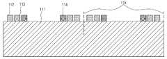
이종 웨이퍼 접합의 열응력 문제를 해결하기 위한 한 가지 다른 접근방법으로 칩 대 웨이퍼 접합이 있다. 예를 들어서 미국 공개특허 2005/0202590 A1에 따른 종래의 웨이퍼레벨 반도체 패키지를 도 1의 단면도와 함께 개략적으로 설명하면 다음과 같다.One other approach to solving the thermal stress problem of heterogeneous wafer bonding is chip to wafer bonding. For example, a conventional wafer level semiconductor package according to US Patent Publication No. 2005/0202590 A1 will be described schematically with the cross-sectional view of FIG. 1 as follows.
종래의 일실시예에 따른 웨이퍼레벨 반도체 패키지는, 도 1에 도시된 바와 같이, 유리 틀(10)과, 상기 틀(10)에 형성된 복수개의 쓰루홀(11)에 각각 삽입된 반도체 소자(20)와, 상기 쓰루홀(11)과 상기 반도체 소자(20) 사이의 공간에 채워진 저 모듈러스 완충 물질(30, low modulus buffer material)과, 상기 전 구성 상에서 일측이 상기 반도체 소자(20)에 전기적으로 연결되고 다른 일측이 외부와 연결된 빌드업층(40), 및 상기 빌드업층(40) 상에 형성된 복수의 전도성 요소(50)로 구성된다.As shown in FIG. 1, the wafer level semiconductor package according to the related art includes a
여기서, 상기 빌드업층(40)은 유전층(41), 전도 트레이스(42), 및 솔더 마스크 층(43)으로 구성되며, 상기 전도성 요소(50)는 솔더 범프와 같은 것으로, 상기 반도체 소자(20)가 외부와 전기적으로 연결되도록 한다.Here, the build-up layer 40 is composed of a
상기 발명은 상기 반도체 소자(20) 보다 크게 제작된 틀(10)과 상기 저 모듈러스 완충 물질(30)에 의해 상기 반도체소자(20)와 그 패키지 사이의 열팽창계수의 차이로 인한 휨, 칩 갈라짐, 그리고 벗겨짐 문제가 근본적으로 해소되는 이점이 있다.According to the present invention, the warpage due to the difference in thermal expansion coefficient between the
상기 발명은 패키지용 틀(10)은 웨이퍼 상태로 구비되는 반면, 반도체 소자(20)는 웨이퍼로부터 분리된 칩 상태로 상기 틀(11)에 실장되는 칩 대 웨이퍼 패키징기술이다. 칩 대 웨이퍼 접합은 칩의 면적이 충분히 작을 경우 열응력으로 인한 부작용이 거의 무시될 수 있고, 또한 칩과 칩 사이의 공간이 열응력을 완충하는 작용을 하여 웨이퍼 대 웨이퍼 접합과 같은 열응력 문제가 발생하지 않는다. 전술한 칩 대 웨이퍼 실장기술은 접합하고자 하는 두 요소, 예를 들어서 칩과 칩 혹은 칩과 패키지의 크기가 서로 다른 경우에 웨이퍼의 불필요한 면적손실을 막을 수 있 는 장점이 있는 반면에 소자 웨이퍼로부터 칩을 분리하고 세정하는 작업, 칩을 접합 웨이퍼에 옮기는 과정, 칩을 웨이퍼에 접합하는 과정, 틀 웨이퍼를 별도로 제작하는 과정 등 제조과정이 매우 복잡하여 제조비용이 웨이퍼 대 웨이퍼 접합에 비해 높은 단점이 있다.The invention is a chip-to-wafer packaging technique in which the
상술한 문제점을 해결하고자 본 출원인은 특허 출원 제2007-0044914호에서 열팽창계수가 상이한 두 웨이퍼를 접합하기 이전에 상기 두 웨이퍼 중 어느 한 웨이퍼를 소정의 접착물질에 의해 복수개의 격자 단위로 분리된 타일형 웨이퍼로 개조함으로써, 상기 타일형 웨이퍼에 나머지 웨이퍼를 고온 접합시 상기 타일형 웨이퍼의 접착물질이 상기 열팽창계수의 불일치로 인해 발생한 열 응력을 흡수, 완화시키도록 하는 타일형 웨이퍼 및 그 제조방법을 출원하였으나, 상기 제조방법은 타일형 웨이퍼의 제조과정이 매우 복잡하고 접착제의 종류와 타일형 웨이퍼의 두께에 따라 타일형 웨이퍼의 제조수율이 달라지는 문제점을 가지고 있다.In order to solve the above problems, the present inventors have applied a tile in which one of the two wafers is separated into a plurality of lattice units by a predetermined adhesive material before bonding two wafers having different thermal expansion coefficients in Patent Application No. 2007-0044914. By converting the wafer into high temperature bonding the remaining wafers to the tile wafer, a tile wafer and a method of manufacturing the tile wafer so that the adhesive material of the tile wafer to absorb and relieve the thermal stress caused by the mismatch of the coefficient of thermal expansion However, the manufacturing method has a problem in that the manufacturing process of the tiled wafer is very complicated and the production yield of the tiled wafer varies depending on the type of adhesive and the thickness of the tiled wafer.
이에 본 발명은 열팽창계수가 상이한 이종 웨이퍼의 고온 접합 시 발생하는 열응력으로 인한 결함발생, 균열, 벗겨짐, 파손 등을 방지할 수 있는 이종 접합 웨이퍼의 제조방법을 제공하는데 목적이 있다. 본 발명의 또 다른 목적은 칩 대 웨이퍼 접합이 갖는 열응력방지 효과를 그대로 활용하면서 동시에 칩 대 웨이퍼 접합 공정을 보다 간단히 제공하는데 목적이 있다. 그리고 본 발명은 상온 접합된 웨이퍼의 접합강도를 높이고 접합균일도 및 신뢰성을 개선하고, 웨이퍼 접합방법과 무관하게 이종 웨이퍼접합시 열응력을 방지할 수 있는 접합웨이퍼의 제조 방법을 제공하는데 또 다른 목적이 있다.Accordingly, an object of the present invention is to provide a method of manufacturing a heterojunction wafer capable of preventing defects, cracks, peeling, and breakage due to thermal stress generated during high temperature bonding of heterogeneous wafers having different thermal expansion coefficients. Another object of the present invention is to provide a chip-to-wafer bonding process more simply while utilizing the thermal stress preventing effect of chip-to-wafer bonding as it is. Another object of the present invention is to provide a method of manufacturing a bonded wafer that can increase the bonding strength of the wafer bonded at room temperature, improve the bonding uniformity and reliability, and prevent thermal stress during the bonding of heterogeneous wafers regardless of the wafer bonding method. have.
또한 본 발명은 이종 웨이퍼간 단순한 기계적 결합과 동시에 접합 웨이퍼내 소자 또는 회로간의 전기적 연결을 통한 기능적 통합을 제공하며, 접합 웨이퍼간 전기적인 연결수단 및 웨이퍼 접합방법과 무관하게 고온 웨이퍼 접합 시 발생 가능한 열응력을 효과적으로 방지하는 방법을 제공하는데 목적이 있다. 그리고, 접합 웨이퍼의 열응력 방지수단으로 인한 웨이퍼의 유효 면적 손실을 방지하는데 목적이 있다.In addition, the present invention provides functional integration through electrical connection between devices or circuits in a bonded wafer at the same time as simple mechanical coupling between different wafers, and heat generated during high temperature wafer bonding regardless of the electrical connection means and the wafer bonding method between the bonded wafers. It is an object to provide a method for effectively preventing stress. In addition, it is an object to prevent the effective area loss of the wafer due to the thermal stress preventing means of the bonded wafer.
본 발명은 이종 웨이퍼 접합용 웨이퍼 및 이종 접합 웨이퍼 제조방법에 관한 것이며, 또한 본 발명에 의해 제조된 접합 웨이퍼에 관한 것이다.The present invention relates to a wafer for heterojunction bonding and a method for producing a heterojunction wafer, and also relates to a bonded wafer produced by the present invention.
웨이퍼의 전 영역을 소정의 면적을 가지는 복수개의 단위격자로 나누고, 상기 단위격자의 경계면 상에 형성되대, 상기 웨이퍼의 상면에서 하부 방향으로 웨이퍼의 두께 보다 얕게 형성되는 채널; 및A channel formed by dividing the entire area of the wafer into a plurality of unit grids having a predetermined area and formed on the boundary surface of the unit grid, and formed to be shallower than the thickness of the wafer in a downward direction from an upper surface of the wafer; And
상기 웨이퍼 상면의 상기 채널 내측에 단수 혹은 복수로 적층되는 이종 웨이퍼와의 접합을 위한 접합수단 및 상기 이종 웨이퍼와의 전기적 연결을 위한 전기적 연결수단;Bonding means for bonding to heterogeneous wafers stacked singly or plurally inside the channel on the upper surface of the wafer and electrical connection means for electrical connection to the heterogeneous wafers;
를 포함하는 것을 특징으로 하는 이종 웨이퍼 접합용 웨이퍼에 관한 것이다.It relates to a wafer for heterojunction bonding comprising a.
상기 접합수단은 이종 웨이퍼와의 접합을 위한 접합수단이며, 상기 접합수단은 ,제 1 접합수단 및 제2접합수단; 를 포함하는 것을 특징으로 한다. 그리고 상기 전기적 연결수단은 제1 접합수단 및 제 2 접합수단 내측에 구비될 수 있다.The bonding means is a bonding means for bonding with a heterogeneous wafer, the bonding means, the first bonding means and the second bonding means; Characterized in that it comprises a. The electrical connection means may be provided inside the first bonding means and the second bonding means.
상기 접합수단은 비전도성 웨이퍼 표면이거나, 폴리머, 솔더 및 금속으로 이루어진 군으로부터 하나 이상 선택된 것을 도포, 진공증착, 화학기상증착, 도금, 스퍼터링으로부터 선택된 하나의 방법으로 형성시킬 수 있다. 또한 상기 전기적 연 결수단은 금속, 솔더 및 전도성 폴리머로부터 선택되는 전도성 물질을 진공증착, 화학기상증착, 도금, 스퍼터링으로부터 선택된 하나의 방법으로 형성시킬 수 있다.The bonding means may be a non-conductive wafer surface, or may be formed by at least one selected from the group consisting of polymers, solders, and metals by one method selected from coating, vacuum deposition, chemical vapor deposition, plating, and sputtering. In addition, the electrical connection means may form a conductive material selected from metal, solder and conductive polymer by one method selected from vacuum deposition, chemical vapor deposition, plating, and sputtering.
본 발명에서 상기 채널은 열경화성 수지, 자외선 경화성 수지 또는 이들의 혼합물인 저탄성 계수(low modulus)응력완충 물질로 채워질 수 있다.In the present invention, the channel may be filled with a low modulus stress buffer material which is a thermosetting resin, an ultraviolet curable resin or a mixture thereof.
이하 본 발명에 따른 이종 접합 웨이퍼 제조방법에 대해 보다 상세히 설명하고자 한다.Hereinafter, a heterojunction wafer manufacturing method according to the present invention will be described in more detail.
본 발명은 a) 제1웨이퍼 및 제2웨이퍼의 전 영역을 소정의 면적을 가지는 복수개의 단위격자로 나누고, 상기 제 1 웨이퍼 및 제2웨이퍼 상면의 상기 각 단위격자 내측에 단수 혹은 복수의 이종 웨이퍼와의 접합을 위한 접합수단 및 이종 웨이퍼와의 전기적 연결수단을 구비하는 단계;The present invention includes a) dividing the entire area of the first wafer and the second wafer into a plurality of unit grids having a predetermined area, and having one or more heterogeneous wafers inside the unit grids on the upper surfaces of the first wafer and the second wafer. Providing bonding means for bonding with and electrical connection with the heterogeneous wafer;
b) 상기 제 1 웨이퍼의 상면에서 상기 단위격자의 경계면을 따라 웨이퍼의 하부 방향으로 웨이퍼의 두께 보다 얕게 채널을 형성하는 단계;b) forming a channel at an upper surface of the first wafer along a boundary of the unit lattice in a lower direction of the wafer than the thickness of the wafer;
c) 상기 제1웨이퍼와 접합될 제2웨이퍼 상면에 상기 제1웨이퍼의 접합수단 및 전기적 연결수단과 대응되게 접합수단 및 전기적 연결수단을 구비하는 단계;c) providing joining means and electrical connecting means on an upper surface of the second wafer to be joined with the first wafer so as to correspond to the joining means and the electrical connecting means of the first wafer;
d) 상기 제 1웨이퍼와 제 2 웨이퍼에서 하나이상 선택되는 접합수단 및 전기적 연결수단을 접하게 하여 상온 접합하는 단계;d) contacting at room temperature by contacting at least one bonding means selected from the first wafer and the second wafer and an electrical connection means;
e) 상기 채널의 일측이 드러나도록 상기 제 1 웨이퍼의 하면을 절삭 및 연마하는 단계; 및e) cutting and polishing the bottom surface of the first wafer to expose one side of the channel; And
f)상기 접합 웨이퍼를 고온에서 2차 접합하는 단계; 를 포함하는 이종 접합 웨이퍼 제조방법에 관한 것이다. 상기 상온 접합 후 , 2차로 고온 접합을 함으로 써, 종래의 반 타일형으로 제조된 제 1 웨이퍼와 제 2 웨이퍼의 고온 접합에 따라 상호 접합되는 웨이퍼 간의 열팽창계수 불일치로 인한 휨 및 파손 문제를 해결 할 수 있다. 또한 본 발명에 따른 접합 웨이퍼 제조방법은 상기 단위격자 사이의 공간이 응력 완충작용을 함으로써 열팽창계수가 서로 다른 이종 웨이퍼의 접합에 유용하게 적용 될 수 있다.f) second bonding the bonded wafer at high temperature; It relates to a heterojunction wafer manufacturing method comprising a. After the normal temperature bonding, by performing the second high temperature bonding, it is possible to solve the problem of warpage and breakage caused by mismatch of thermal expansion coefficient between the first wafer manufactured in the conventional half-tile type and the wafer bonded to each other according to the high temperature bonding of the second wafer. Can be. In addition, the bonded wafer manufacturing method according to the present invention can be usefully applied to the bonding of heterogeneous wafers having different thermal expansion coefficients by the space between the unit grids and the stress buffering action.
본 발명에 따른 접합 웨이퍼 제조방법에서 상기 제 1 웨이퍼 및 제 2 웨이퍼는 전기, 기계, 광, 센서, 바이오 소자 중 어느 하나 또는 둘 이상의 소자가 미리 형성된 소자 웨이퍼이거나 또는 제 1 웨이퍼 또는 제 2 웨이퍼 중 어느 하나는 전기, 기계, 광, 센서, 바이오 소자 중 어느 하나 또는 둘 이상의 소자가 형성된 소자 웨이퍼이고, 다른 하나는 상기 소자 웨이퍼를 웨이퍼레벨 패키징하기 위한 캡 웨이퍼일 수 있으며, 상기 제 1 웨이퍼가 캡 웨이퍼이고, 상기 제 2 웨이퍼가 소자 웨이퍼인 것이 제조 공정의 용이성 측면에서 더욱 바람직하다. 상기 제1웨이퍼 및 제2 웨이퍼가 둘 다 또는 어느 한 웨이퍼가 소자 웨이퍼인 경우 상기 소자 웨이퍼는 적어도 2매 이상의 웨이퍼가 적층된 적층(stack) 웨이퍼 일 수 있다.In the method of manufacturing a bonded wafer according to the present invention, the first wafer and the second wafer may be a device wafer in which any one or more of electrical, mechanical, optical, sensor, and bio devices are pre-formed or among the first wafer or the second wafer. One may be a device wafer on which any one or more of electrical, mechanical, optical, sensor, or bio devices are formed, and the other may be a cap wafer for wafer-level packaging of the device wafer, and the first wafer may be a cap. It is more preferable that it is a wafer and a said 2nd wafer is an element wafer from a viewpoint of the ease of a manufacturing process. When both the first wafer and the second wafer or one of the wafers is a device wafer, the device wafer may be a stack wafer in which at least two or more wafers are stacked.
상기 a)단계에서 상기 접합수단은 소자의 밀봉수단으로 사용될 수 있으며, 또한 전기적 연결의 수단으로 사용될 수 있다. 상기 제 1 접합수단 및 전기적 연결수단은 상기 소자 웨이퍼 및 캡 웨이퍼의 용도에 따라 위치가 달라질 수 있다.In the step a), the bonding means may be used as a sealing means of the device and may also be used as a means of electrical connection. The first bonding means and the electrical connection means may vary in position depending on the use of the device wafer and the cap wafer.
상기 a)단계에서 상기 제 1 웨이퍼 및 제2웨이퍼는 실리콘반도체, 화합물반도체, 유리, 세라믹, LTCC 및 압전소재 중 선택된 어느 하나 이상의 물질을 기판 으로 할 수 있으며, 상기 압전소재는 LiNbO3, LiTaO3, PZT, 석영(quartz) 중에서 선택된 어느 1종 이상의 물질을 기판으로 할 수 있다.In step a), the first wafer and the second wafer may be made of at least one material selected from silicon semiconductor, compound semiconductor, glass, ceramic, LTCC, and piezoelectric material, and the piezoelectric material may be LiNbO3 , LiTaO3. One or more materials selected from among PZT and quartz may be used as the substrate.
본 발명은 상기 a)단계에서 제 1 웨이퍼의 접합수단은 상기 단위격자의 내측 상면에 구비되는 제 1 접합수단과 제 2 접합수단으로 구성되어진 것을 특징으로 하며, 상기 a)단계에서 제1 접합수단; 제 2접합수단; 또는 제 1 및 제 2 접합수단;는 전기적 연결수단이 될 수 있다.The present invention is characterized in that the joining means of the first wafer in step a) is composed of a first joining means and a second joining means provided on the inner upper surface of the unit grid, the first joining means in step a) ; Second joining means; Alternatively, the first and second bonding means may be electrical connection means.
상기 a)단계에서 상기 접합수단은 비전도성 웨이퍼 표면이거나, 폴리머, 솔더 및 금속으로 이루어진 군으로부터 하나이상 선택된 것을 도포, 진공증착, 화학기상증착, 도금, 스퍼터링으로부터 선택된 하나의 방법으로 형성시킬수 있으며, 상기 전기적 연결수단은 이종 웨이퍼와의 접합을 위한 접합수단인 것을 특징으로 한다.In the step a), the bonding means may be formed on a non-conductive wafer surface, or at least one selected from the group consisting of polymers, solders, and metals by one method selected from coating, vacuum deposition, chemical vapor deposition, plating, and sputtering. The electrical connection means is characterized in that the bonding means for bonding with different wafers.
상기 d)단계에서 상온 접합은 직접접합, 압착 및 접착제 접합에서 선택된 어느 한 방법을 이용할 수 있다. 상기 상온 접합은 제 1 웨이퍼와 제 2웨이퍼와의 접합 시 열에 의한 스트레스가 발생하지 않도록 상온에서 이루어지며, 상기 e)단계에서 제 1 웨이퍼 및 제 2 웨이퍼가 분리되지 않게 수행할 수 있도록 한다. 보다 구체적으로 상온 접합은 직접접합법을 이용할 수 있으며, 상기 직접접합은 표면 활성화 접합(surface activated bonding)방법을 사용할 수 있다.Room temperature bonding in step d) may use any one method selected from direct bonding, pressing and adhesive bonding. The room temperature bonding is performed at room temperature so that stress due to heat does not occur when the first wafer and the second wafer are bonded, and the first wafer and the second wafer may be separated from each other in the step e). More specifically, room temperature bonding may use a direct bonding method, and the direct bonding may use a surface activated bonding method.
상기 f)단계에서 고온접합은 열처리(Annealing), 양극접합(anodic bonding), 열-압착접착(thermo-compression bonding), 유텍틱접합(eutectic bonding), 접착제 접합(adhesive bonding), 솔더접합(solder bonding)중 선택된 어느 한 방법을 이용할 수 있다. 상기 고온접합 온도가 150℃ 미만인 경우 접합 강도가 약할 수 있으며, 상기 온도가 400℃를 초과하는 경우 열에 의한 스트레스에 의해 웨이퍼 자체의 물리적 변형을 유발하거나 소자의 특성에 영향을 줄 수 있어 바람직하지 못하다. 상기 2차 고온 웨이퍼 접합은 제 1 웨이퍼 및 제 2 웨이퍼의 전기적 연결과 동시에 이루어질 수 있으며, 이 때 2차 고온 웨이퍼 접합은 금속 등 도전성 물질 간의 접합에 의해 이루어질 수 있다.In the f) step, the high temperature bonding is performed by annealing, anodizing, thermo-compression bonding, eutectic bonding, adhesive bonding, solder bonding. You can use either method selected. If the high temperature bonding temperature is less than 150 ℃ bond strength may be weak, if the temperature exceeds 400 ℃ heat stress may cause physical deformation of the wafer itself or may affect the characteristics of the device is not preferred. . The second high temperature wafer bonding may be performed at the same time as the electrical connection between the first wafer and the second wafer, and the second high temperature wafer bonding may be performed by bonding between a conductive material such as a metal.
상기 b)단계 후, 상기 채널에 열경화성 수지, 자외선 경화성 수지 또는 이들의 혼합물인 저탄성 계수(low modulus)응력완충 물질을 채워서 경화시키는 단계를 더 포함할 수 있으며, 보다 구체적으로는 실리콘 수지, 에폭시, 레진, 폴리이미드, 아크릴계 수지로부터 하나이상 선택된 물질을 채워서 경화시킬 수 있다. 상기 응력 완충물질은 상온 접합의 낮은 접합강도로 인한 단위격자의 이탈을 방지하는데 효과적이다.After the step b), the channel may further include a step of curing by filling a low modulus stress buffer material, which is a thermosetting resin, an ultraviolet curable resin, or a mixture thereof, and more specifically, a silicone resin and an epoxy. One or more materials selected from resins, resins, polyimides and acrylic resins may be filled and cured. The stress buffer material is effective to prevent the separation of the unit grid due to the low bond strength of the room temperature junction.
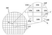
상기 b)단계에서 단위격자는 칩 사이즈의 정수배의 면적을 가지고, 상기 채널은 상기 제 1웨이퍼 및 제 2 웨이퍼를 개별 칩으로 분리할 때 칩과 칩사이의 경계면에 위치하는 것이 바람직하다.In the step b), the unit grid has an area of an integer multiple of the chip size, and the channel is preferably located at an interface between the chip and the chip when the first wafer and the second wafer are separated into individual chips.
그리고, 상기 b)단계에서 채널의 폭은 상기 제 1 웨이퍼 및 상기 제 2 웨이퍼를 개별칩으로 분리할 때 소잉 폭과 같거나 더 작게 함으로써 채널로 인한 웨이퍼의 유효면적 손실을 방지한다. 또한 본 발명에서 채널의 폭(Wch)은 하기 식1의 관계식을 가진다.In the step b), the width of the channel is equal to or smaller than the sawing width when the first wafer and the second wafer are separated into individual chips, thereby preventing the loss of the effective area of the wafer due to the channel. In addition, in the present invention, the channel width Wch has a relational expression of the following Equation 1.
[식1][Equation 1]
Wch≥D×nWch ≥D × n
( 상기 D는 고온접합온도에서 웨이퍼내 단위격자의 최대 열팽창 증가폭이며, 상기n은 n≥2인 정수이다.)(D is the maximum increase in thermal expansion of the unit lattice in the wafer at a high temperature bonding temperature, and n is an integer of n≥2.)
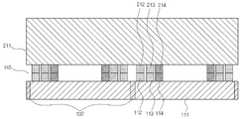
본 발명은 상기 f) 단계 후, g)단계로 고온접합된 제 1 웨이퍼 또는 제 2 웨이퍼에 상기 제 1 웨이퍼 또는 제 2 웨이퍼를 관통하는 관통비아를 형성하는 단계;After the step f), the step of forming a through via penetrating the first wafer or the second wafer on the first wafer or the second wafer hot-bonded in step g);
상기 관통비아에 금속을 채워서 금속패드를 형성하는 단계; 및Filling the through via with metal to form a metal pad; And
솔더 범프를 형성하는 단계;를 더 포함하는 것을 특징으로 하는 이종 접합 웨이퍼 제조방법을 제공한다. 본 발명은 상기 방법으로 제조된 접합 웨이퍼에 관한 것이며,이종 웨이퍼를 이용한 웨이퍼레벨 패키징과 이종 웨이퍼의 조합을 통한 하이브리드 소자의 제조에 관한 것이다.Forming a solder bump; provides a heterojunction wafer manufacturing method further comprising. TECHNICAL FIELD The present invention relates to a bonded wafer manufactured by the above method, and relates to the manufacture of a hybrid device through a combination of wafer-level packaging using a heterogeneous wafer and a heterogeneous wafer.
본 발명에 따른 이종 접합 웨이퍼 제조방법은 웨이퍼 대 웨이퍼 접합을 상온에서 실시하여 열팽창계수의 차로 인한 열응력 문제를 해소하고, 접합 웨이퍼 중 어느 한 웨이퍼를 복수의 격자로 분리하여 칩 대 웨이퍼 접합 상태로 만든 다음에 고온 접합을 실시함으로써 웨이퍼 대 웨이퍼 접합의 열응력 문제를 해소하고 동시에 칩 대 웨이퍼 접합의 복잡한 공정을 보다 간단히 할 수 있는 효과가 있다.The heterojunction wafer manufacturing method according to the present invention performs the wafer-to-wafer bonding at room temperature to solve the thermal stress caused by the difference in the coefficient of thermal expansion, and separates any one wafer from the bonded wafer into a plurality of lattice to a chip-to-wafer bonding state. After the high temperature bonding, the thermal stress problem of the wafer-to-wafer bonding can be solved and the complicated process of chip-to-wafer bonding can be simplified.
보다 구체적으로 상면에 채널이 형성된 제 1 웨이퍼를 제 2 웨이퍼와 상온 접합하고, 제 1 웨이퍼의 하면을 절삭 연마한 후 2차 고온 접합을 시행함으로써, 고온 접합에 따라 상호 접합되는 웨이퍼 간의 열팽창계수 불일치로 인한 휨 및 파손 문제를 완전히 해결할 수 있으며, 이종 웨이퍼간 웨이퍼레벨 패키징 공정에서 웨이퍼 간의 접합 신뢰성을 현저히 향상시킬 수 있다.More specifically, the first wafer having a channel formed on the upper surface is bonded to the second wafer at room temperature, and the lower surface of the first wafer is cut and polished, followed by secondary high temperature bonding, thereby inconsistent coefficients of thermal expansion between the wafers bonded to each other due to the high temperature bonding. It is possible to completely solve the warpage and breakage caused by the process, and to significantly improve the wafer-to-wafer reliability in the wafer-to-wafer packaging process.
따라서 본 발명에 따른 이종 접합 웨이퍼 제조방법은 상온 웨이퍼 접합의 낮은 접합강도와 웨이퍼내 접합균일성 그리고 낮은 수율과 신뢰성 문제를 개선하여 열팽창계수가 서로 다른 이종 웨이퍼 간 웨이퍼 접합을 용이하게 함으로써 다양한 종류의 이종 웨이퍼간 접합을 통해 소자의 기능성 밀도를 보다 증가시킴은 물론 새로운 기능성 소자의 제조에 이용될 수 있다.Therefore, the heterojunction wafer fabrication method according to the present invention improves the low bond strength, intra-wafer bond uniformity, low yield and reliability problems of room temperature wafer bonding, thereby facilitating wafer bonding between different wafers having different thermal expansion coefficients. Heterogeneous wafer-to-wafer bonding further increases the functional density of the device and can be used to manufacture new functional devices.
이하, 본 발명의 바람직한 실시예를 첨부한 도면에 의거하여 더욱 상세하게 설명하면 다음과 같다.Hereinafter, with reference to the accompanying drawings, preferred embodiments of the present invention in more detail as follows.
하기 도 2는 본 발명의 일 실시예에 따른 접합웨이퍼의 제조방법을 도시한 것이다. 본 발명에 따른 일 실시예는 접합에 참여하는 제 1 웨이퍼(100) 및 제 2 웨이퍼(200)이 구비되고, 상기 제 1 웨이퍼(100)에 대해서 제 1 접합수단, 제 2 접합수단, 전기적 연결수단을 형성하는 단계(110); 상기 제 2 웨이퍼(200)에 대해서 상기 제 1 웨이퍼(100)와 대응되는 제 1 접합수단, 제 2 접합수단, 전기적 연결수단을 형성하는 단계(210); 상기 제 1 웨이퍼(100)에 대해서 반 절단 채널을 형성하는 단계(130); 상기 제 1웨이퍼(100)의 상면에 제 2 웨이퍼(200)을 상온에서 1차 접합시키는 단계(140); 제 1 웨이퍼(100)의 하면을 절삭 및 연마하는 단계(150);와 상온접합 웨이퍼를 고온 접합하는 단계(160)로 이루어진다.2 shows a method of manufacturing a bonded wafer according to an embodiment of the present invention. One embodiment according to the present invention is provided with a
상기 제 1 웨이퍼 및 제 2 웨이퍼는 전기, 기계, 광, 센서, 바이오 소자 중 어느 하나 또는 둘 이상의 소자가 형성된 소자 웨이퍼(device wafer)이거나, 상기 제 1웨이퍼 및 제 2 웨이퍼 중 어느 하나가 소자 웨이퍼이고, 다른 하나는 상기 소자 웨이퍼를 웨이퍼레벨 패키징을 하기 위한 캡(cap) 웨이퍼 일 수 있다. 상기 제 1 웨이퍼 및 제 2 웨이퍼가 둘 다 또는 한 웨이퍼가 소자 웨이퍼인 경우, 상기 소자 웨이퍼는 2매 이상의 웨이퍼가 적층된 적층(stack) 웨이퍼 일 수 있다.The first wafer and the second wafer are device wafers in which any one or more of electrical, mechanical, optical, sensor, and bio devices are formed, or one of the first wafer and the second wafer is a device wafer. And the other may be a cap wafer for wafer level packaging of the device wafer. When both the first wafer and the second wafer or one wafer is a device wafer, the device wafer may be a stack wafer in which two or more wafers are stacked.
그리고, 상기 제 1 웨이퍼(100)과 제 2 웨이퍼(200)중 어느 하나가 캡 웨이퍼인 경우 상기 제 1 웨이퍼(100)을 캡 웨이퍼로 하는 것이 제조공정을 보다 용이하게 할 수 있어 바람직한 방법이다. 상기 캡 웨이퍼는 캐비티, 관통비아, 수동소자로 이루어진 군으로부터 선택된 어느 하나 이상을 구비한 것일 수 있다. 본 발명은 접합되는 웨이퍼의 종류와 열팽창 계수 차이의 크기에 무관한 이종 웨이퍼간 접합 방법을 제공하므로, 상기 제 1 웨이퍼(100) 및 제 2 웨이퍼(200)의 소재에 크게 제한 받지 않는다. 단지, 본 발명의 분야가 전기.전자소자, MEMS, 광소자, 센서 등의 소자와 이들의 웨이퍼레벨 패키징에 관한 것이므로 상기 제 1 웨이퍼(100)과 제 2 웨이퍼(200)는 상기 분야에서 통상적으로 사용되는 실리콘반도체, 화합물반도체, 압전물질, 세라믹, 유리, LTCC/HTCC등의 소재를 기판으로하는 것이 바람직하다. 상기 제 2웨이퍼(200)은 접합 반대면, 즉 하면에 상면의 소자 및 회로와 연결되는 관통 비아(through wafer via) 및 금속패드가 미리 형성된 것일 수 있다.In addition, when any one of the
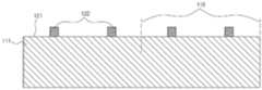
하기 도 3 및 4를 참고하여 본 발명을 좀더 상세히 설명하고자 한다. 도 3은 본 발명의 일 실시예에 따라 제 1 접합수단(112), 제 2 접합수단(113) 및 전기적 연결수단(114)를 구비한 제 1 웨이퍼의 일부분을 나타낸 평면도이다. 하기 도 4는 상기 도 3의 절개면(115)에 따라 절개된 단면도이다. 상기 도 3은 상온접합을 위한 제 1 접합수단(112), 고온접합을 위한 제 2 접합수단(113) 및 웨이퍼간 전기적 연결을 위한 전기적 연결수단(114)가 서로 다른 위치에 각각 구비된 일 실시예이다.Hereinafter, the present invention will be described in more detail with reference to FIGS. 3 and 4. 3 is a plan view of a portion of a first wafer having a first bonding means 112, a second bonding means 113, and an electrical connecting means 114, in accordance with an embodiment of the present invention. 4 is a cross-sectional view taken along the cutting
상기 제 1 접합수단(112), 제 2 접합수단(113) 및 전기적 연결수단(114)는 모두 동일한 물질로 구성될 수도 있고 또는 서로 다른 물질로 구성될 수 있다. 상기 제 1 접합수단(112)는 접합 웨이퍼의 하면 절삭단계(150) 및 그 이후에 적어도 접합된 웨이퍼 또는 칩이 분리되지 않을 정도의 접합강도를 제공하는 접합 수단으로써, 바람직하게는 열응력이 발생하지 않는 상온 직접접합 또는 저온에서 가능한 압착 또는 접착제 접합 등에 필요한 접합물질이 구비된다.The first bonding means 112, the second bonding means 113, and the electrical connecting means 114 may all be made of the same material or different materials. The first bonding means 112 is a bonding means for providing a bonding strength such that at least the wafer or chip bonded to the lower surface of the bonded wafer after the cutting
상기 제 1 접합수단(112)는 상기 도 3과 같이 각 칩의 경계면(116) 내측에 단수 또는 복수로 구비되되, 제2접합수단(113) 및 전기적 연결수단(114)를 제외한 전 영역에 형성될 수 있으나, 바람직하게는 각 칩의 소자 영역(117) 외곽에서 소자 영역(117)을 에워싸는 형태가 바람직하다. 상기 제 1접합수단은 상온 직접접합이 가능한 제 1 웨이퍼 표면일 수 있고, 또는 역시 상온 직접접합이 가능한 Al, Cu, Au, AuSn, Sn, In, Sn-alloy로 이루어진 군으로부터 하나 이상 선택된 금속 및 솔더를 진공증착, 도금, 화학기상증착, 스퍼터링 등으로 형성하거나 비전도성 폴리머를 코팅하여 제공된다.The first bonding means 112 is provided in the singular or plural inside the
상기 제 2 접합수단(113)는 고온접합단계(160)에서 약 150℃이상의 고온 접합에 필요한 접합 수단으로써, 각 칩의 경계면(116) 내측에 단수 또는 복수로 구비 되되, 제1접합수단(113) 및 전기적 연결수단(114)를 제외한 전 영역에 형성될 수 있으나, 바람직하게는 칩의 소자영역(117) 외곽에서 소자영역(117)을 에워싸는 형태가 바람직하다. 경우에 따라서 상기 제 2 접합수단은 제 1 접합수단과 동일할 수 있으며, 이때 상온 접합된 제 1 접합수단(112)를 고온 열처리함으로써 제2접합수단(113)의 역할을 수행한다. 고온 접합은 단순한 열처리 과정일 수 있고 또는 열과 함께 압력, 전압, 초음파 등을 인가하는 양극접합, 열-압착접합, 유텍틱 접합 또는 솔더 접합 중에서 선택된 어느 한가지 방법으로 할 수 있다. 그리고 상기 제 1 접합수단(112) 및 제 2 접합수단(113)은 소자영역(117) 외곽에 형성되어 소자영역(117)을 외부 환경으로부터 보호하는 소자의 밀봉 수단을 겸할 수 있다. 상기 제 2접합수단(113)은 상온 직접접합에 사용된 제 1 웨이퍼의 비전도성 표면일 수 있고, 또는 Al, Cu, Au, AuSn, Sn, Sn-alloy로 이루어진 군으로부터 하나 이상 선택된 금속 및 솔더를 진공증착, 도금, 화학기상증착, 스퍼터링 등으로 형성하여 제공된다.The second bonding means 113 is a bonding means necessary for high temperature bonding of about 150 ° C. or higher in the high
상기 전기적 연결수단(114)는 접합 웨이퍼 간의 전기적 연결을 제공할 수 있는 모든 수단이 사용될 수 있으며, 구체적으로 각 칩의 경계면(116) 내측에 복수로 구비되되, 바람직하게는 칩의 소자 영역(117) 내측에 하나 이상의 접촉패드(contact pads)로 구성된다. 전기적 연결수단(114)의 바람직한 소재로는 고온 접합온도 이하에서 접합이 가능한 전도성 물질, 보다 구체적으로 Al, Cu, Au로부터 선택되는 금속, AuSn, Sn, In, Sn-alloy로부터 선택되는 솔더 또는 전도성 폴리머가 사용된다. 상기 전기적 연결부(114)는 적어도 2층 이상의 다층금속막으로 구성 되되, 그 최외곽층은 Au, Cu, Al, Au/Sn, Sn, In, Sn-alloy 중 선택된 어느 하나로 구비되는 것이 바람직하다. 전기적 연결수단은 통상적으로 반도체제조에서 사용되는 도금, 진공증착, 스퍼터링, 코팅 등의 방법으로 형성된다.All means for providing an electrical connection between the bonded wafers may be used as the electrical connection means 114. Specifically, a plurality of means are provided inside the
상기 제 1 접합수단(112), 제 2 접합수단(113), 전기적 연결수단(114)는 순서에 관계없이 구비될 수 있다. 상기 제 1 접합수단(112), 제 2 접합수단(113), 전기적 연결수단(114)는 각각 서로 다른 물질로 구비될 수도 있고, 2개 이상이 같은 물질로 구비 될 수 있다. 구체적인 예시로는 금속간 직접접합을 상온접합 수단으로 이용하고 후속 열처리를 통한 고온접합을 사용할 경우에는 금속간 접합을 통해 접합 웨이퍼간의 기계적 접합과 전기적 연결을 동시에 제공할 수 있어, 제 1, 제2 접합수단 및 전기적 연결수단은 모두 동일한 금속으로 구비되는 것이 가능하다. 그리고 금속 또는 솔더물질로 된 접합수단 및 전기적 연결수단은 적어도 2층 이상의 다층금속막으로 구성되되, 그 최외곽층은 Au, Cu, Al, Au/Sn, Sn, In, Sn-alloy 중 선택된 어느 하나로 구비되는 것이 바람직하다.The first bonding means 112, the second bonding means 113, and the electrical connecting means 114 may be provided in any order. The first bonding means 112, the second bonding means 113, the electrical connection means 114 may be provided with different materials, respectively, two or more may be provided with the same material. As a specific example, in the case of using a direct bonding between metals as a room temperature bonding means and using a high temperature bonding through subsequent heat treatment, it is possible to simultaneously provide mechanical and electrical connection between bonded wafers through intermetallic bonding. Both the joining means and the electrical connecting means can be provided with the same metal. The joining means and the electrical connecting means made of metal or solder material are composed of at least two or more multilayer metal films, and the outermost layer is any one selected from Au, Cu, Al, Au / Sn, Sn, In, and Sn-alloy. It is preferable that one is provided.
하기 도5는 본 발명에 따른 제 1 웨이퍼에서 제 1 접합수단으로 폴리머 또는 에폭시 등의 저온 접착물질을 사용하는 경우의 제 1 웨이퍼의 단면도를 나타낸 것이다. 제 1 접합수단(117)는 전기적 연결수단(118) 및 제 2 접합수단(119)를 제외한 전 영역에 형성된다. 전기적 연결수단(118)은 칩 경계면(116) 내측에 단수 또는 복수로 구비되고, 바람직하게는 칩의 소자 영역(117) 내측에 하나 이상의 접촉패드(contact pads)로 구성된다.5 is a cross-sectional view of the first wafer when a low temperature adhesive material such as polymer or epoxy is used as the first bonding means in the first wafer according to the present invention. The first joining
하기 도 6은 본 발명에 따른 접합수단이 제 1웨이퍼 자체로서, 직접접합을 이용하여 상온에서 접합하고 2차로 고온에서 열처리하는 경우의 단면도이다. 상기 도 6은 웨이퍼 자신이 직접접합 수단이 되는 경우로 직접접합을 이용하여 상온에서 1차로 웨이퍼 접합을 수행하고 2차적인 고온접합을 통해 보다 완전한 웨이퍼-웨이퍼간 및 금속-금속간 접합을 달성하는 경우이다. 상기 직접접합시 제 1 접합수단(121)은 패드형태로 구비될 필요가 없으며, 전기적 연결수단(122)를 제외한 웨이퍼 상면의 모든 영역에 구비 될 수 있다. 상기 직접접합은 금속범프가 형성된 두 웨이퍼의 표면을 진공 혹은 상압에서 플라즈마로 표면처리하는 표면활성화접합 방법과, 불화 실리콘 디옥사이드(fluorinated silicon dioxide) 등 별도의 접합층을 웨이퍼 표면에 형성 하는 접합 방법이 사용 될 수 있다.6 is a cross-sectional view when the bonding means according to the present invention is the first wafer itself, and is bonded at room temperature using direct bonding and heat-treated at a high temperature in a secondary manner. FIG. 6 illustrates that the wafer is used as a direct bonding means in which wafer bonding is performed at a room temperature using primary bonding, and secondary wafer bonding is used to achieve more complete wafer-wafer and metal-metal bonding. If it is. In the direct bonding, the
하기 도 7은 본 발명에 따른 제 2 웨이퍼의 단면도를 나타낸 것이다. 하기 도 7은 제 1접합수단(212), 제 2 접합수단(213), 전기적 연결수단(214)가 구비된 제 2 웨이퍼(211)로 제 1웨이퍼와 동일한 방법으로 제조가 가능하므로 구체적인 설명은 생략하기로 한다.7 shows a cross-sectional view of a second wafer according to the present invention. 7 is a
하기 도 8 은 본 발명에 따른 반절단(half cutting) 채널이 형성된 제 1 웨이퍼의 일부를 나타낸 단면도이고, 하기 도 9는 본 발명에 따른 반절단 채널이 형성된 제 1 웨이퍼를 개략적으로 도시한 도면이다. 하기 도 8과 같이 제 1 웨이퍼(111)의 상면에 건식식각(dry ething), 레이저 천공(laser drilling), 소잉톱 날(sawing blade)를 사용한 반 절단(half cutting) 및 습식 에칭(wet ething)으로 이루어진 군으로부터 하나이상 선택된 방법으로 상기 제 1 웨이퍼(111)의 두께보다 얕은 깊이(134)와 소잉폭 보다 작은 폭(135)을 가진 복수의 채널(132)을 형성한다.8 is a cross-sectional view showing a portion of a first wafer having a half cutting channel according to the present invention, and FIG. 9 is a view schematically showing a first wafer having a half cutting channel according to the present invention. . As shown in FIG. 8, dry etching, laser drilling, half cutting and wet etching using a sawing blade are performed on the upper surface of the
하기 도 9의 평면도를 보면, 상기 채널(132)는 제1 웨이퍼(111)의 상면에 웨이퍼의 전면을 가로지르는 격자 형으로 형성함으로써 단위격자(110a 내지 110i)가 형성된다. 상기 단위격자의 면적은 상기 제 1 웨이퍼(111) 또는 제 2 웨이퍼(211)의 칩 (또는 다이) 사이즈와 같고, 상기 채널은 칩과 칩 사이의 경계면(116), 즉 장차 소잉될 위치에 형성하며, 상기 채널의 폭(135)는 소잉되는 폭과 같거나 더 작게 함으로써 상기 채널로 인한 웨이퍼의 면적손실을 방지할 수 있다. 상기 채널의 폭(135)는 고온에서 2차 접합 시 단위격자의 최대 열팽창 증가폭의 두 배 이상인 것이 바람직하다. 상기 칩의 사이즈가 열응력으로 인한 부작용이 나타날 수 있는 크기보다 작을 경우, 상기 단위격자의 면적은 칩사이즈의 정수배로 할 수 있다. 상기 채널(132)는 폴리머 등의 저탄성 응력완충 물질로 채우는 것도 가능하다.Referring to the plan view of FIG. 9, the
하기 도 10은 제 1 웨이퍼 및 제 2웨이퍼의 상온 접합단계(140)을 개략적으로 나타낸 단면도이다. 하기 도 11은 상온 접합단계(140)가 완료된 제 1 웨이퍼(211) 및 제 2 웨이퍼(121)의 단면도이다. 이하 상온 접합단계(140)를 보다 상세히 설명하고자 한다.10 is a cross-sectional view schematically illustrating a room
단계(110)을 통해 제 1접합수단(112), 제 2 접합수단(113), 전기적 연결수단(113)가 구비되고 채널형성단계(120)에서 형성된 채널(132)를 구비한 제 1 웨이 퍼와; 단계(210)을 통해 제 1접합수단(212), 제 2 접합수단(213) 및 전기적 연결수단(214)를 구비한 제 2웨이퍼;를 정렬장치에서 서로 정렬하여 소정의 지그에 장착한 다음 웨이퍼 접합 장치를 이용하여 상온에서 직접접합, 압착, 또는 접착제접합에서 선택된 어느 한가지 방법으로 접합한다. 상기 상온 접합시 온도는 반드시 상온에만 국한되는 것이 아니라 열응력이 무시될 수 있는 온도로써 150 ℃ 이하가 바람직하며, 압착 및 접착제 접합 시는 열 이외에 압력을 인가하는 것이 바람직하고, 인가되는 압력의 범위는 제한되지 않는다. 직접접합시는 진공 또는 상압에서 플라즈마를 이용한 표면활성화단계를 더 추가할 수 있다. 이때 접합웨이퍼 간의 정렬은 표면 처리에 이용된 동일한 챔버 내에서 이루어지는 것이 바람직하다. 상기 상온 직접접합 방법은 종래기술에서 언급하였으므로 보다 구체적인 설명은 생략하도록 한다.A first wafer having a first bonding means 112, a second bonding means 113, an electrical connecting means 113, and having a
하기 도 12는 제 1 웨이퍼의 하면을 절삭 및 연마하는 단계(150)을 나타낸 단면도이다. 상기 도11의 상온 접합 웨이퍼(145)에서 제 1 웨이퍼(111)의 하면을 절삭(grinding) 및 화학물리적 연마(chemical mechanical polishing) 하여 상기 반 절단 채널(132)의 일부분이 드러나도록 한다. 따라서 제1웨이퍼의 하면절삭단계(150)을 통해 상기 반절단 채널(132)로 구분된 복수개의 단위격자(110a 내지 110i)는 서로 완전히 분리되어 상온 접합 웨이퍼(145)는 칩 대 웨이퍼 접합구조로 변환되게 된다. 본 발명에서는 웨이퍼 대 웨이퍼 접합을 간단히 칩 대 웨이퍼 접합으로 변환시키는 방법을 제공함으로써 고온 웨이퍼 접합으로 인한 열응력이 완전히 제거되는 효과를 나타낼 수 있다.12 is a cross-sectional view illustrating a
마지막으로 고온 접합단계(160)로서 고온접합은 제 1 웨이퍼(111)에 대한 단계(110)에서 형성된 제 1 접합수단(112), 제 2 접합수단(113) 및 전기적 연결수단(114) 와 제 2 웨이퍼(211)에 대한 단계(210)에서 형성된 제 1 접합수단(212), 제 2 접합수단(213) 및 전기적 연결수단(214)가 모두 참여하여 이루어진다. 이 단계를 통해 상기 제 1 및 제2 접합수단과 전기적 연결수단은 완전한 물리적 결합을 이루게된다. 고온접합 방법으로는 단순히 열처리를 통하여 상온접합의 강도를 보다 높이는 방법; 열과 함께 압력, 초음파, 전압 등을 인가하는 방법을 들 수 있으며, 보다 구체적으로는 양극접합, 열-압착, 유텍틱접합, 솔더접합을 사용할 수 있다. 상기 고온 접합의 온도는 150℃ 내지 400℃에서 수행하는 것이 바람직하다. 상기 전기적 연결수단의 물리적 결합은 상온 접합을 통해서도 일부 가능하지만, 고온 접합을 통해 보다 강한 물리적 결합을 달성할 수 있다.Finally, as the high
본 발명에 따른 접합 웨이퍼 제조방법은 제 1 또는 제 2 웨이퍼의 하면에 관통비아(310)을 형성하는 단계; 상기 관통비아 외벽에 절연막을 형성하는 단계; 상기 관통비아에 금속을 채워서 금속패드(320)을 형성하는 단계; PCB기판 접합용 솔더 범프(330)을 형성하는 단계를 더 추가할 수 있다. 하기 도 13은 본 발명에 따른 접합웨이퍼 제조 후 추가적으로 관통비아, 금속패드 및 솔더범프를 형성하는 단계를 개략적으로 나타낸 단면도이다. 하기 도 13 a)는 본 발명에 따른 제 1 웨이퍼(111)과 제 2 웨이퍼(211)가 접합된 접합웨이퍼(300)가 구비되고, b)단계로, 채 널(132)에 포토레지스트 또는 폴리머를 채우고 열 또는 자외선으로 경화시킨다. 이는 제 1 웨이퍼(111)의 하면을 평탄하게 하여 이후 공정을 용이하게 하기 위한 것이다. c)단계로, 제1 웨이퍼(111)의 하면에 통상적인 반도체 사진 전사공정과 건식식각 또는 습식식각 공정으로 상기 웨이퍼 상면의 전기적 연결수단(114)와 연결되는 관통비아(310)을 형성하고, 상기 관통비아(310)과 기판과의 전기적 절연을 위하여 패럴린(parylene), 실리콘산화막, 또는 실리콘 질화막을 상기 관통비아(310)측벽과 제 1 웨이퍼(111)의 후면에 형성시킨다. d)단계로 상기 제 1웨이퍼의 후면과, 관통비아(310)을 연결하는 금속패드(320)을 구비하고, e)단계로 외부 PCB와 기계적 결합 및 전기적 연결을 위한 솔더범프(330)을 형성한다.In accordance with another aspect of the present invention, a method of manufacturing a bonded wafer includes forming a through via 310 on a bottom surface of a first or second wafer; Forming an insulating film on the outer wall of the through via; Filling the through via with metal to form a metal pad (320); Forming a
상기한 실시예들은 이종 웨이퍼접합을 통하여 접합 웨이퍼간의 물리적인 결합과 동시에 전기적인 연결을 제공하는 방법에 관한 것이다. 그러나 본 발명의 반 절단 채널을 구비한 웨이퍼는 상기한 목적 이외에 타 용도로 얼마던지 전용이 가능하다. 일 예로서 본 발명의 반 절단 채널을 구비한 웨이퍼는 이종 에피텍셜성장용 기판으로서 이용가능하다. 그리고 본 명세서와 도면에는 본 발명의 바람직한 실시예에 대하여 개시하였으며, 비록 특정한 용어들이 사용되었으나, 이는 단지 본 발명의 기술 내용을 쉽게 설명하고 독자의 이해를 돕기 위한 일반적인 의미에서 사용된 것이지, 본 발명의 범위를 한정하고자 하는 것은 아니다. 일 예로서 본 발명에서 사용한 상온이란 접합 시 열응력을 최소화하기 위한 방편으로 사용한 것이지 특정한 온도를 지칭한 것은 아니다. 여기에 개시된 실시예 외에도 본 발명의 기술적 사상에 바탕을 둔 다른 변형예들이 실시 가능하다는 것은 본 발명이 속하는 기술분 야에서 통상의 지식을 가진 자에게는 자명한 것이다. 본 발명의 범위는 후술하는 특허청구범위에 나타난다.The above embodiments are directed to a method of providing electrical connection simultaneously with physical bonding between bonded wafers through heterogeneous wafer bonding. However, the wafer with the semi-cut channel of the present invention can be used for any other purpose other than the above-described purposes. As an example, a wafer having a half cut channel of the present invention can be used as a substrate for heteroepitaxial growth. In the present specification and drawings, preferred embodiments of the present invention have been disclosed. Although specific terms have been used, these are merely used in a general sense to easily explain the technical contents of the present invention and to help the readers understand the present invention. It is not intended to limit the scope of. As an example, the room temperature used in the present invention is used as a means for minimizing thermal stress during bonding, and does not refer to a specific temperature. It will be apparent to those skilled in the art that other modifications based on the technical idea of the present invention can be carried out in addition to the embodiments disclosed herein. The scope of the invention is shown in the following claims.
도 1은 종래의 웨이퍼 레벨 반도체 패키지의 제조방법을 개략적으로 도시한 공정단면도이다.1 is a process cross-sectional view schematically showing a conventional method for manufacturing a wafer level semiconductor package.
도 2는 본 발명의 일 실시예에 따른 접합웨이퍼의 제조방법을 도시한 것이다.2 illustrates a method of manufacturing a bonded wafer according to an embodiment of the present invention.
도 3은 본 발명에 따른 제 1 웨이퍼의 평면도이다.3 is a plan view of a first wafer according to the present invention.
도 4는 상기 도 3의 절개면(115)에 따라 절개된 단면도를 나타낸 것이다.4 is a cross-sectional view taken along the cutting
도 5는 본 발명에 따른 제 1 웨이퍼에서 제 1 접합수단이 폴리머 또는 접착제이고, 전기적 연결수단이 제 2 접합수단을 겸하는 경우의 단면도를 나타낸 것이다.FIG. 5 shows a cross-sectional view when the first bonding means is a polymer or an adhesive and the electrical connecting means also serves as the second bonding means in the first wafer according to the present invention.
도 6은 본 발명에 따른 접합수단이 제 1웨이퍼로, 직접접합을 이용하여 상온에서 접합하는 경우의 웨이퍼의 단면도이다.6 is a cross-sectional view of the wafer in the case where the bonding means according to the present invention is the first wafer and is bonded at room temperature using direct bonding.
도 7은 본 발명에 따른 제 2 웨이퍼의 단면도를 나타낸 것이다.7 shows a cross-sectional view of a second wafer according to the present invention.
도 8 은 본 발명에 따른 채널이 형성된 제 1 웨이퍼를 나타낸 단면도이다.8 is a cross-sectional view showing a first wafer having a channel according to the present invention.
도 9는 본 발명에 따른 채널이 형성된 제 1 웨이퍼를 개략적으로 도시한 도면이다.9 is a view schematically showing a first wafer on which a channel is formed according to the present invention.
도 10은 제 1 웨이퍼 및 제 2웨이퍼의 상온 접합단계를 개략적으로 나타낸 단면도이다.10 is a cross-sectional view schematically illustrating a step of attaching a first wafer and a second wafer to room temperature.
도 11은 상온 접합단계가 완료된 제 1 웨이퍼 및 제 2 웨이퍼의 단면도이다.11 is a cross-sectional view of the first wafer and the second wafer where the normal temperature bonding step is completed.
도 12는 제 1 웨이퍼의 하면을 절삭 및 연마하는 단계를 나타낸 단면도이다.12 is a cross-sectional view illustrating a step of cutting and polishing a lower surface of the first wafer.
도 13은 본 발명에 따른 접합웨이퍼 제조후 추가적으로 관통비아, 금속패드 및 솔더범프를 형성하는 단계를 개략적으로 나타낸 단면도이다.FIG. 13 is a schematic cross-sectional view illustrating a step of forming through vias, metal pads, and solder bumps after fabrication of a bonded wafer according to the present invention.
[도면의 주요 부분에 대한 부호설명][Code Description of Main Parts of Drawing]
110a 내지 110i; 단위격자111; 제 1 웨이퍼110a to 110i;
112,117,121,212; 제 1 접합수단112,117,121,212; First joining means
113,213; 제 2 접합수단113,213; Second joining means
114,118,122,214; 전기적 연결수단114,118,122,214; Electrical connection means
115; 절개면116; 칩경계117; 소자영역132;채널115;
133; 단위격자의 폭134; 채널 깊이135; 채널의 폭133; Width of the
211;제 2 웨이퍼310;관통비아 320;금속패드 330;솔더범프211;
Claims (32)
Translated fromKoreanPriority Applications (1)
| Application Number | Priority Date | Filing Date | Title |
|---|---|---|---|
| US12/796,798US8241961B2 (en) | 2008-12-09 | 2010-06-09 | Method for manufacturing hetero-bonded wafer |
Applications Claiming Priority (2)
| Application Number | Priority Date | Filing Date | Title |
|---|---|---|---|
| KR1020080124607 | 2008-12-09 | ||
| KR20080124607 | 2008-12-09 |
Publications (1)
| Publication Number | Publication Date |
|---|---|
| KR100945800B1true KR100945800B1 (en) | 2010-03-05 |
Family
ID=42183002
Family Applications (1)
| Application Number | Title | Priority Date | Filing Date |
|---|---|---|---|
| KR1020090050859AExpired - Fee RelatedKR100945800B1 (en) | 2008-12-09 | 2009-06-09 | Method for manufacturing heterogeneous bonded wafer |
Country Status (2)
| Country | Link |
|---|---|
| US (1) | US8241961B2 (en) |
| KR (1) | KR100945800B1 (en) |
Cited By (6)
| Publication number | Priority date | Publication date | Assignee | Title |
|---|---|---|---|---|
| US8486758B2 (en) | 2010-12-20 | 2013-07-16 | Tessera, Inc. | Simultaneous wafer bonding and interconnect joining |
| KR101341531B1 (en)* | 2012-02-14 | 2013-12-13 | 한국생산기술연구원 | Apparatus for manufacturing metal-ceramic fine layered composite materials by HV-SCDB (High Vacuum Surface Controlled Direct Bonding) |
| KR101405561B1 (en)* | 2012-07-19 | 2014-06-10 | 현대자동차주식회사 | MEMS sensor packaging method |
| KR20140079499A (en)* | 2011-10-21 | 2014-06-26 | 코닌클리케 필립스 엔.브이. | Low warpage wafer bonding through use of slotted substrates |
| KR20200029067A (en)* | 2015-06-12 | 2020-03-17 | 소이텍 | Heterostructure and method of fabrication |
| US12334461B2 (en) | 2022-09-06 | 2025-06-17 | Globalfoundries U.S. Inc. | Bonding structure using two oxide layers with different stress levels, and related method |
Families Citing this family (77)
| Publication number | Priority date | Publication date | Assignee | Title |
|---|---|---|---|---|
| US6962835B2 (en) | 2003-02-07 | 2005-11-08 | Ziptronix, Inc. | Method for room temperature metal direct bonding |
| US7485968B2 (en) | 2005-08-11 | 2009-02-03 | Ziptronix, Inc. | 3D IC method and device |
| KR100945800B1 (en)* | 2008-12-09 | 2010-03-05 | 김영혜 | Method for manufacturing heterogeneous bonded wafer |
| DE102009029180B4 (en)* | 2009-09-03 | 2017-07-20 | Robert Bosch Gmbh | microsystems |
| US20110151114A1 (en)* | 2009-12-18 | 2011-06-23 | Cooledge Lighting, Inc. | Composite patterning device and method for removing elements from host substrate by establishing conformal contact between device and a contact surface |
| US8697493B2 (en)* | 2011-07-18 | 2014-04-15 | Soitec | Bonding surfaces for direct bonding of semiconductor structures |
| TWI493690B (en)* | 2011-07-18 | 2015-07-21 | Soitec Silicon On Insulator | Improved bonding surfaces for direct bonding of semiconductor structures |
| FR2992466A1 (en)* | 2012-06-22 | 2013-12-27 | Soitec Silicon On Insulator | CONTACT IMPLEMENTATION METHOD FOR LED AND RESULTING STRUCTURE |
| NL2009757C2 (en) | 2012-11-05 | 2014-05-08 | Micronit Microfluidics Bv | Method for forming an electrically conductive via in a substrate. |
| CN103824787B (en)* | 2012-11-16 | 2016-09-07 | 中国科学院上海微系统与信息技术研究所 | Wafer bonding method based on bonding agent |
| US9202963B2 (en)* | 2012-11-21 | 2015-12-01 | Taiwan Semiconductor Manufacturing Company, Ltd. | Dual-side illumination image sensor chips and methods for forming the same |
| JP2014103291A (en)* | 2012-11-21 | 2014-06-05 | Renesas Electronics Corp | Semiconductor device manufacturing method |
| US20150262902A1 (en) | 2014-03-12 | 2015-09-17 | Invensas Corporation | Integrated circuits protected by substrates with cavities, and methods of manufacture |
| US11069734B2 (en) | 2014-12-11 | 2021-07-20 | Invensas Corporation | Image sensor device |
| US9741620B2 (en) | 2015-06-24 | 2017-08-22 | Invensas Corporation | Structures and methods for reliable packages |
| US10431624B2 (en)* | 2015-07-08 | 2019-10-01 | Samsung Electronics Co., Ltd. | Method of manufacturing image sensor including nanostructure color filter |
| US10886250B2 (en) | 2015-07-10 | 2021-01-05 | Invensas Corporation | Structures and methods for low temperature bonding using nanoparticles |
| JP6608640B2 (en)* | 2015-07-28 | 2019-11-20 | 新光電気工業株式会社 | Manufacturing method of mounting structure |
| US9953941B2 (en) | 2015-08-25 | 2018-04-24 | Invensas Bonding Technologies, Inc. | Conductive barrier direct hybrid bonding |
| US9852988B2 (en) | 2015-12-18 | 2017-12-26 | Invensas Bonding Technologies, Inc. | Increased contact alignment tolerance for direct bonding |
| US10446532B2 (en) | 2016-01-13 | 2019-10-15 | Invensas Bonding Technologies, Inc. | Systems and methods for efficient transfer of semiconductor elements |
| US10204893B2 (en) | 2016-05-19 | 2019-02-12 | Invensas Bonding Technologies, Inc. | Stacked dies and methods for forming bonded structures |
| US10483215B2 (en)* | 2016-09-22 | 2019-11-19 | International Business Machines Corporation | Wafer level integration including design/co-design, structure process, equipment stress management and thermal management |
| US10446487B2 (en) | 2016-09-30 | 2019-10-15 | Invensas Bonding Technologies, Inc. | Interface structures and methods for forming same |
| US10580735B2 (en) | 2016-10-07 | 2020-03-03 | Xcelsis Corporation | Stacked IC structure with system level wiring on multiple sides of the IC die |
| US10672745B2 (en)* | 2016-10-07 | 2020-06-02 | Xcelsis Corporation | 3D processor |
| TWI822659B (en) | 2016-10-27 | 2023-11-21 | 美商艾德亞半導體科技有限責任公司 | Structures and methods for low temperature bonding |
| US10002844B1 (en) | 2016-12-21 | 2018-06-19 | Invensas Bonding Technologies, Inc. | Bonded structures |
| TWI837879B (en) | 2016-12-29 | 2024-04-01 | 美商艾德亞半導體接合科技有限公司 | Bonded structures with integrated passive component |
| US10276909B2 (en) | 2016-12-30 | 2019-04-30 | Invensas Bonding Technologies, Inc. | Structure comprising at least a first element bonded to a carrier having a closed metallic channel waveguide formed therein |
| EP3580166A4 (en) | 2017-02-09 | 2020-09-02 | Invensas Bonding Technologies, Inc. | Bonded structures |
| WO2018169968A1 (en) | 2017-03-16 | 2018-09-20 | Invensas Corporation | Direct-bonded led arrays and applications |
| US10515913B2 (en) | 2017-03-17 | 2019-12-24 | Invensas Bonding Technologies, Inc. | Multi-metal contact structure |
| US10508030B2 (en) | 2017-03-21 | 2019-12-17 | Invensas Bonding Technologies, Inc. | Seal for microelectronic assembly |
| US10784191B2 (en) | 2017-03-31 | 2020-09-22 | Invensas Bonding Technologies, Inc. | Interface structures and methods for forming same |
| US10879212B2 (en) | 2017-05-11 | 2020-12-29 | Invensas Bonding Technologies, Inc. | Processed stacked dies |
| US10446441B2 (en) | 2017-06-05 | 2019-10-15 | Invensas Corporation | Flat metal features for microelectronics applications |
| US10217720B2 (en) | 2017-06-15 | 2019-02-26 | Invensas Corporation | Multi-chip modules formed using wafer-level processing of a reconstitute wafer |
| US10840205B2 (en) | 2017-09-24 | 2020-11-17 | Invensas Bonding Technologies, Inc. | Chemical mechanical polishing for hybrid bonding |
| US11380597B2 (en) | 2017-12-22 | 2022-07-05 | Invensas Bonding Technologies, Inc. | Bonded structures |
| US10923408B2 (en) | 2017-12-22 | 2021-02-16 | Invensas Bonding Technologies, Inc. | Cavity packages |
| US11169326B2 (en) | 2018-02-26 | 2021-11-09 | Invensas Bonding Technologies, Inc. | Integrated optical waveguides, direct-bonded waveguide interface joints, optical routing and interconnects |
| US11256004B2 (en) | 2018-03-20 | 2022-02-22 | Invensas Bonding Technologies, Inc. | Direct-bonded lamination for improved image clarity in optical devices |
| US11056348B2 (en) | 2018-04-05 | 2021-07-06 | Invensas Bonding Technologies, Inc. | Bonding surfaces for microelectronics |
| US10790262B2 (en) | 2018-04-11 | 2020-09-29 | Invensas Bonding Technologies, Inc. | Low temperature bonded structures |
| US11244916B2 (en) | 2018-04-11 | 2022-02-08 | Invensas Bonding Technologies, Inc. | Low temperature bonded structures |
| CN108447795B (en)* | 2018-04-16 | 2020-03-17 | 歌尔股份有限公司 | Bonding method of LED wafer |
| US11004757B2 (en) | 2018-05-14 | 2021-05-11 | Invensas Bonding Technologies, Inc. | Bonded structures |
| US11276676B2 (en) | 2018-05-15 | 2022-03-15 | Invensas Bonding Technologies, Inc. | Stacked devices and methods of fabrication |
| KR20210009426A (en) | 2018-06-13 | 2021-01-26 | 인벤사스 본딩 테크놀로지스 인코포레이티드 | TV as a pad |
| US11393779B2 (en) | 2018-06-13 | 2022-07-19 | Invensas Bonding Technologies, Inc. | Large metal pads over TSV |
| US11158606B2 (en) | 2018-07-06 | 2021-10-26 | Invensas Bonding Technologies, Inc. | Molded direct bonded and interconnected stack |
| US11462419B2 (en) | 2018-07-06 | 2022-10-04 | Invensas Bonding Technologies, Inc. | Microelectronic assemblies |
| US20200044621A1 (en)* | 2018-07-31 | 2020-02-06 | Qualcomm Incorporated | Thin film devices |
| US11515291B2 (en) | 2018-08-28 | 2022-11-29 | Adeia Semiconductor Inc. | Integrated voltage regulator and passive components |
| US11011494B2 (en) | 2018-08-31 | 2021-05-18 | Invensas Bonding Technologies, Inc. | Layer structures for making direct metal-to-metal bonds at low temperatures in microelectronics |
| US11158573B2 (en) | 2018-10-22 | 2021-10-26 | Invensas Bonding Technologies, Inc. | Interconnect structures |
| DE102018132644B4 (en) | 2018-12-18 | 2020-08-06 | RF360 Europe GmbH | Microacoustic package at wafer level and manufacturing process |
| US11244920B2 (en) | 2018-12-18 | 2022-02-08 | Invensas Bonding Technologies, Inc. | Method and structures for low temperature device bonding |
| CN113330557A (en) | 2019-01-14 | 2021-08-31 | 伊文萨思粘合技术公司 | Bonding structure |
| US11901281B2 (en) | 2019-03-11 | 2024-02-13 | Adeia Semiconductor Bonding Technologies Inc. | Bonded structures with integrated passive component |
| US12374641B2 (en) | 2019-06-12 | 2025-07-29 | Adeia Semiconductor Bonding Technologies Inc. | Sealed bonded structures and methods for forming the same |
| US11296053B2 (en) | 2019-06-26 | 2022-04-05 | Invensas Bonding Technologies, Inc. | Direct bonded stack structures for increased reliability and improved yield in microelectronics |
| US12080672B2 (en) | 2019-09-26 | 2024-09-03 | Adeia Semiconductor Bonding Technologies Inc. | Direct gang bonding methods including directly bonding first element to second element to form bonded structure without adhesive |
| US11762200B2 (en) | 2019-12-17 | 2023-09-19 | Adeia Semiconductor Bonding Technologies Inc. | Bonded optical devices |
| WO2021236361A1 (en) | 2020-05-19 | 2021-11-25 | Invensas Bonding Technologies, Inc. | Laterally unconfined structure |
| US11631647B2 (en) | 2020-06-30 | 2023-04-18 | Adeia Semiconductor Bonding Technologies Inc. | Integrated device packages with integrated device die and dummy element |
| US11764177B2 (en) | 2020-09-04 | 2023-09-19 | Adeia Semiconductor Bonding Technologies Inc. | Bonded structure with interconnect structure |
| US11728273B2 (en) | 2020-09-04 | 2023-08-15 | Adeia Semiconductor Bonding Technologies Inc. | Bonded structure with interconnect structure |
| US11264357B1 (en) | 2020-10-20 | 2022-03-01 | Invensas Corporation | Mixed exposure for large die |
| JP7514530B2 (en) | 2020-10-29 | 2024-07-11 | 東北マイクロテック株式会社 | Stacked semiconductor device |
| CN112599431A (en)* | 2020-12-15 | 2021-04-02 | 联合微电子中心有限责任公司 | Wafer bonding structure and bonding method |
| JP2024501017A (en) | 2020-12-28 | 2024-01-10 | アデイア セミコンダクター ボンディング テクノロジーズ インコーポレイテッド | Structure with through-substrate via and method for forming the same |
| JP2024501559A (en) | 2020-12-30 | 2024-01-12 | アデイア セミコンダクター ボンディング テクノロジーズ インコーポレイテッド | Structures with conductive features and methods of forming the same |
| US11742320B2 (en)* | 2021-03-11 | 2023-08-29 | Taiwan Semiconductor Manufacturing Company, Ltd. | Wafer bonding alignment |
| CN113808964B (en)* | 2021-09-23 | 2024-04-26 | 华东光电集成器件研究所 | Heterogeneous eutectic method based on multiple chips and small size |
| CN114743956A (en)* | 2022-04-08 | 2022-07-12 | 北京灵汐科技有限公司 | Wafer-level system, method for generating same, method for processing data, and storage medium |
Citations (2)
| Publication number | Priority date | Publication date | Assignee | Title |
|---|---|---|---|---|
| JP2008153326A (en)* | 2006-12-15 | 2008-07-03 | Elpida Memory Inc | Manufacturing method of semiconductor device |
| KR20080099408A (en)* | 2007-05-09 | 2008-11-13 | (주) 파이오닉스 | Tile type wafer and its manufacturing method |
Family Cites Families (7)
| Publication number | Priority date | Publication date | Assignee | Title |
|---|---|---|---|---|
| US5965933A (en)* | 1996-05-28 | 1999-10-12 | Young; William R. | Semiconductor packaging apparatus |
| EP1351288B1 (en)* | 2002-04-05 | 2015-10-28 | STMicroelectronics Srl | Process for manufacturing an insulated interconnection through a body of semiconductor material and corresponding semiconductor device |
| US7109092B2 (en)* | 2003-05-19 | 2006-09-19 | Ziptronix, Inc. | Method of room temperature covalent bonding |
| FR2856844B1 (en)* | 2003-06-24 | 2006-02-17 | Commissariat Energie Atomique | HIGH PERFORMANCE CHIP INTEGRATED CIRCUIT |
| US7358586B2 (en)* | 2004-09-28 | 2008-04-15 | International Business Machines Corporation | Silicon-on-insulator wafer having reentrant shape dielectric trenches |
| US8664747B2 (en)* | 2008-04-28 | 2014-03-04 | Toshiba Techno Center Inc. | Trenched substrate for crystal growth and wafer bonding |
| KR100945800B1 (en)* | 2008-12-09 | 2010-03-05 | 김영혜 | Method for manufacturing heterogeneous bonded wafer |
- 2009
- 2009-06-09KRKR1020090050859Apatent/KR100945800B1/ennot_activeExpired - Fee Related
- 2010
- 2010-06-09USUS12/796,798patent/US8241961B2/ennot_activeExpired - Fee Related
Patent Citations (2)
| Publication number | Priority date | Publication date | Assignee | Title |
|---|---|---|---|---|
| JP2008153326A (en)* | 2006-12-15 | 2008-07-03 | Elpida Memory Inc | Manufacturing method of semiconductor device |
| KR20080099408A (en)* | 2007-05-09 | 2008-11-13 | (주) 파이오닉스 | Tile type wafer and its manufacturing method |
Cited By (15)
| Publication number | Priority date | Publication date | Assignee | Title |
|---|---|---|---|---|
| US8486758B2 (en) | 2010-12-20 | 2013-07-16 | Tessera, Inc. | Simultaneous wafer bonding and interconnect joining |
| US8709913B2 (en) | 2010-12-20 | 2014-04-29 | Tessera, Inc. | Simultaneous wafer bonding and interconnect joining |
| KR20140079499A (en)* | 2011-10-21 | 2014-06-26 | 코닌클리케 필립스 엔.브이. | Low warpage wafer bonding through use of slotted substrates |
| KR102020001B1 (en)* | 2011-10-21 | 2019-09-09 | 루미리즈 홀딩 비.브이. | Low warpage wafer bonding through use of slotted substrates |
| KR101341531B1 (en)* | 2012-02-14 | 2013-12-13 | 한국생산기술연구원 | Apparatus for manufacturing metal-ceramic fine layered composite materials by HV-SCDB (High Vacuum Surface Controlled Direct Bonding) |
| KR101405561B1 (en)* | 2012-07-19 | 2014-06-10 | 현대자동차주식회사 | MEMS sensor packaging method |
| KR20200029067A (en)* | 2015-06-12 | 2020-03-17 | 소이텍 | Heterostructure and method of fabrication |
| US10826459B2 (en) | 2015-06-12 | 2020-11-03 | Soitec | Heterostructure and method of fabrication |
| KR20200145848A (en)* | 2015-06-12 | 2020-12-30 | 소이텍 | Heterostructure and method of fabrication |
| KR102285595B1 (en)* | 2015-06-12 | 2021-08-04 | 소이텍 | Heterostructure and method of fabrication |
| KR102301378B1 (en)* | 2015-06-12 | 2021-09-14 | 소이텍 | Heterostructure and method of fabrication |
| US11595020B2 (en) | 2015-06-12 | 2023-02-28 | Soitec | Heterostructure and method of fabrication |
| US11637542B2 (en) | 2015-06-12 | 2023-04-25 | Soitec | Heterostructure and method of fabrication |
| US12101080B2 (en) | 2015-06-12 | 2024-09-24 | Soitec | Heterostructure and method of fabrication |
| US12334461B2 (en) | 2022-09-06 | 2025-06-17 | Globalfoundries U.S. Inc. | Bonding structure using two oxide layers with different stress levels, and related method |
Also Published As
| Publication number | Publication date |
|---|---|
| US8241961B2 (en) | 2012-08-14 |
| US20100308455A1 (en) | 2010-12-09 |
Similar Documents
| Publication | Publication Date | Title |
|---|---|---|
| KR100945800B1 (en) | Method for manufacturing heterogeneous bonded wafer | |
| US9812406B2 (en) | Microelectronic assemblies with cavities, and methods of fabrication | |
| TWI590332B (en) | Heterogeneous annealing method and device | |
| US9899281B2 (en) | Integrated circuits protected by substrates with cavities, and methods of manufacture | |
| KR20240130111A (en) | A combined structure having interconnecting assemblies | |
| KR101765966B1 (en) | Window interposed die packaging | |
| KR100609806B1 (en) | Manufacturing method of semiconductor device | |
| CN102844861B (en) | TCE Compensation for Assembled IC Package Substrates for Die Warpage Reduction | |
| TWI687986B (en) | Method for manufacturing chip package | |
| US20110217826A1 (en) | Method of fabricating semiconductor device | |
| US20160329304A1 (en) | Semiconductor device and method of manufacturing semiconductor device | |
| KR20050121432A (en) | Method for forming thin wafer stack for wafer level package | |
| TWI512940B (en) | Method for bonding of chips on wafers | |
| JP2005501414A (en) | Method and printed circuit package for forming contacts | |
| WO2011093955A2 (en) | Dual carrier for joining ic die or wafers to tsv wafers | |
| TW201110310A (en) | Method for forming an integrated circuit structure and integrated circuit structure | |
| KR20150060758A (en) | Semiconductor device and method for manufacturing same | |
| US9799626B2 (en) | Semiconductor packages and other circuit modules with porous and non-porous stabilizing layers | |
| US20110147905A1 (en) | Semiconductor device and method of manufacturing the same | |
| US7868336B2 (en) | Semiconductor device and method of manufacturing the same | |
| TW202125651A (en) | Method of manufacturing semiconductor device and collet | |
| KR100924269B1 (en) | Tile type wafer and its manufacturing method | |
| CN113314399A (en) | Grinding sheet packaging structure and grinding sheet method for bonding wafers | |
| CN110610952B (en) | Image sensor device and manufacturing method thereof | |
| TWI425580B (en) | Process for manufacturing semiconductor chip packaging module |
Legal Events
| Date | Code | Title | Description |
|---|---|---|---|
| A201 | Request for examination | ||
| PA0109 | Patent application | St.27 status event code:A-0-1-A10-A12-nap-PA0109 | |
| PA0201 | Request for examination | St.27 status event code:A-1-2-D10-D11-exm-PA0201 | |
| A302 | Request for accelerated examination | ||
| PA0302 | Request for accelerated examination | St.27 status event code:A-1-2-D10-D17-exm-PA0302 St.27 status event code:A-1-2-D10-D16-exm-PA0302 | |
| D13-X000 | Search requested | St.27 status event code:A-1-2-D10-D13-srh-X000 | |
| D14-X000 | Search report completed | St.27 status event code:A-1-2-D10-D14-srh-X000 | |
| E902 | Notification of reason for refusal | ||
| PE0902 | Notice of grounds for rejection | St.27 status event code:A-1-2-D10-D21-exm-PE0902 | |
| E13-X000 | Pre-grant limitation requested | St.27 status event code:A-2-3-E10-E13-lim-X000 | |
| P11-X000 | Amendment of application requested | St.27 status event code:A-2-2-P10-P11-nap-X000 | |
| P13-X000 | Application amended | St.27 status event code:A-2-2-P10-P13-nap-X000 | |
| E701 | Decision to grant or registration of patent right | ||
| PE0701 | Decision of registration | St.27 status event code:A-1-2-D10-D22-exm-PE0701 | |
| GRNT | Written decision to grant | ||
| PR0701 | Registration of establishment | St.27 status event code:A-2-4-F10-F11-exm-PR0701 | |
| PR1002 | Payment of registration fee | St.27 status event code:A-2-2-U10-U11-oth-PR1002 Fee payment year number:1 | |
| PG1601 | Publication of registration | St.27 status event code:A-4-4-Q10-Q13-nap-PG1601 | |
| FPAY | Annual fee payment | Payment date:20130220 Year of fee payment:4 | |
| PR1001 | Payment of annual fee | St.27 status event code:A-4-4-U10-U11-oth-PR1001 Fee payment year number:4 | |
| LAPS | Lapse due to unpaid annual fee | ||
| PC1903 | Unpaid annual fee | St.27 status event code:A-4-4-U10-U13-oth-PC1903 Not in force date:20140227 Payment event data comment text:Termination Category : DEFAULT_OF_REGISTRATION_FEE | |
| PC1903 | Unpaid annual fee | St.27 status event code:N-4-6-H10-H13-oth-PC1903 Ip right cessation event data comment text:Termination Category : DEFAULT_OF_REGISTRATION_FEE Not in force date:20140227 |