KR100945372B1 - Multi-domain liquid crystal display device - Google Patents
Multi-domain liquid crystal display deviceDownload PDFInfo
- Publication number
- KR100945372B1 KR100945372B1KR1020020088454AKR20020088454AKR100945372B1KR 100945372 B1KR100945372 B1KR 100945372B1KR 1020020088454 AKR1020020088454 AKR 1020020088454AKR 20020088454 AKR20020088454 AKR 20020088454AKR 100945372 B1KR100945372 B1KR 100945372B1
- Authority
- KR
- South Korea
- Prior art keywords
- liquid crystal
- pixel
- domain
- substrate
- crystal display
- Prior art date
- Legal status (The legal status is an assumption and is not a legal conclusion. Google has not performed a legal analysis and makes no representation as to the accuracy of the status listed.)
- Expired - Fee Related
Links
Images


Classifications
- G—PHYSICS
- G02—OPTICS
- G02F—OPTICAL DEVICES OR ARRANGEMENTS FOR THE CONTROL OF LIGHT BY MODIFICATION OF THE OPTICAL PROPERTIES OF THE MEDIA OF THE ELEMENTS INVOLVED THEREIN; NON-LINEAR OPTICS; FREQUENCY-CHANGING OF LIGHT; OPTICAL LOGIC ELEMENTS; OPTICAL ANALOGUE/DIGITAL CONVERTERS
- G02F1/00—Devices or arrangements for the control of the intensity, colour, phase, polarisation or direction of light arriving from an independent light source, e.g. switching, gating or modulating; Non-linear optics
- G02F1/01—Devices or arrangements for the control of the intensity, colour, phase, polarisation or direction of light arriving from an independent light source, e.g. switching, gating or modulating; Non-linear optics for the control of the intensity, phase, polarisation or colour
- G02F1/13—Devices or arrangements for the control of the intensity, colour, phase, polarisation or direction of light arriving from an independent light source, e.g. switching, gating or modulating; Non-linear optics for the control of the intensity, phase, polarisation or colour based on liquid crystals, e.g. single liquid crystal display cells
- G02F1/133—Constructional arrangements; Operation of liquid crystal cells; Circuit arrangements
- G02F1/1333—Constructional arrangements; Manufacturing methods
- G02F1/1337—Surface-induced orientation of the liquid crystal molecules, e.g. by alignment layers
- G02F1/133707—Structures for producing distorted electric fields, e.g. bumps, protrusions, recesses, slits in pixel electrodes
- G—PHYSICS
- G02—OPTICS
- G02F—OPTICAL DEVICES OR ARRANGEMENTS FOR THE CONTROL OF LIGHT BY MODIFICATION OF THE OPTICAL PROPERTIES OF THE MEDIA OF THE ELEMENTS INVOLVED THEREIN; NON-LINEAR OPTICS; FREQUENCY-CHANGING OF LIGHT; OPTICAL LOGIC ELEMENTS; OPTICAL ANALOGUE/DIGITAL CONVERTERS
- G02F1/00—Devices or arrangements for the control of the intensity, colour, phase, polarisation or direction of light arriving from an independent light source, e.g. switching, gating or modulating; Non-linear optics
- G02F1/01—Devices or arrangements for the control of the intensity, colour, phase, polarisation or direction of light arriving from an independent light source, e.g. switching, gating or modulating; Non-linear optics for the control of the intensity, phase, polarisation or colour
- G02F1/13—Devices or arrangements for the control of the intensity, colour, phase, polarisation or direction of light arriving from an independent light source, e.g. switching, gating or modulating; Non-linear optics for the control of the intensity, phase, polarisation or colour based on liquid crystals, e.g. single liquid crystal display cells
- G02F1/133—Constructional arrangements; Operation of liquid crystal cells; Circuit arrangements
- G02F1/1333—Constructional arrangements; Manufacturing methods
- G02F1/1337—Surface-induced orientation of the liquid crystal molecules, e.g. by alignment layers
- G—PHYSICS
- G02—OPTICS
- G02F—OPTICAL DEVICES OR ARRANGEMENTS FOR THE CONTROL OF LIGHT BY MODIFICATION OF THE OPTICAL PROPERTIES OF THE MEDIA OF THE ELEMENTS INVOLVED THEREIN; NON-LINEAR OPTICS; FREQUENCY-CHANGING OF LIGHT; OPTICAL LOGIC ELEMENTS; OPTICAL ANALOGUE/DIGITAL CONVERTERS
- G02F1/00—Devices or arrangements for the control of the intensity, colour, phase, polarisation or direction of light arriving from an independent light source, e.g. switching, gating or modulating; Non-linear optics
- G02F1/01—Devices or arrangements for the control of the intensity, colour, phase, polarisation or direction of light arriving from an independent light source, e.g. switching, gating or modulating; Non-linear optics for the control of the intensity, phase, polarisation or colour
- G02F1/13—Devices or arrangements for the control of the intensity, colour, phase, polarisation or direction of light arriving from an independent light source, e.g. switching, gating or modulating; Non-linear optics for the control of the intensity, phase, polarisation or colour based on liquid crystals, e.g. single liquid crystal display cells
- G02F1/133—Constructional arrangements; Operation of liquid crystal cells; Circuit arrangements
- G02F1/1333—Constructional arrangements; Manufacturing methods
- G02F1/1335—Structural association of cells with optical devices, e.g. polarisers or reflectors
- G02F1/133509—Filters, e.g. light shielding masks
- G02F1/133512—Light shielding layers, e.g. black matrix
- G—PHYSICS
- G02—OPTICS
- G02F—OPTICAL DEVICES OR ARRANGEMENTS FOR THE CONTROL OF LIGHT BY MODIFICATION OF THE OPTICAL PROPERTIES OF THE MEDIA OF THE ELEMENTS INVOLVED THEREIN; NON-LINEAR OPTICS; FREQUENCY-CHANGING OF LIGHT; OPTICAL LOGIC ELEMENTS; OPTICAL ANALOGUE/DIGITAL CONVERTERS
- G02F1/00—Devices or arrangements for the control of the intensity, colour, phase, polarisation or direction of light arriving from an independent light source, e.g. switching, gating or modulating; Non-linear optics
- G02F1/01—Devices or arrangements for the control of the intensity, colour, phase, polarisation or direction of light arriving from an independent light source, e.g. switching, gating or modulating; Non-linear optics for the control of the intensity, phase, polarisation or colour
- G02F1/13—Devices or arrangements for the control of the intensity, colour, phase, polarisation or direction of light arriving from an independent light source, e.g. switching, gating or modulating; Non-linear optics for the control of the intensity, phase, polarisation or colour based on liquid crystals, e.g. single liquid crystal display cells
- G02F1/133—Constructional arrangements; Operation of liquid crystal cells; Circuit arrangements
- G02F1/1333—Constructional arrangements; Manufacturing methods
- G02F1/1337—Surface-induced orientation of the liquid crystal molecules, e.g. by alignment layers
- G02F1/133753—Surface-induced orientation of the liquid crystal molecules, e.g. by alignment layers with different alignment orientations or pretilt angles on a same surface, e.g. for grey scale or improved viewing angle
- G02F1/133761—Surface-induced orientation of the liquid crystal molecules, e.g. by alignment layers with different alignment orientations or pretilt angles on a same surface, e.g. for grey scale or improved viewing angle with different pretilt angles
- G—PHYSICS
- G02—OPTICS
- G02F—OPTICAL DEVICES OR ARRANGEMENTS FOR THE CONTROL OF LIGHT BY MODIFICATION OF THE OPTICAL PROPERTIES OF THE MEDIA OF THE ELEMENTS INVOLVED THEREIN; NON-LINEAR OPTICS; FREQUENCY-CHANGING OF LIGHT; OPTICAL LOGIC ELEMENTS; OPTICAL ANALOGUE/DIGITAL CONVERTERS
- G02F1/00—Devices or arrangements for the control of the intensity, colour, phase, polarisation or direction of light arriving from an independent light source, e.g. switching, gating or modulating; Non-linear optics
- G02F1/01—Devices or arrangements for the control of the intensity, colour, phase, polarisation or direction of light arriving from an independent light source, e.g. switching, gating or modulating; Non-linear optics for the control of the intensity, phase, polarisation or colour
- G02F1/13—Devices or arrangements for the control of the intensity, colour, phase, polarisation or direction of light arriving from an independent light source, e.g. switching, gating or modulating; Non-linear optics for the control of the intensity, phase, polarisation or colour based on liquid crystals, e.g. single liquid crystal display cells
- G02F1/133—Constructional arrangements; Operation of liquid crystal cells; Circuit arrangements
- G02F1/136—Liquid crystal cells structurally associated with a semi-conducting layer or substrate, e.g. cells forming part of an integrated circuit
- G02F1/1362—Active matrix addressed cells
- G02F1/1368—Active matrix addressed cells in which the switching element is a three-electrode device
Landscapes
- Physics & Mathematics (AREA)
- Nonlinear Science (AREA)
- Spectroscopy & Molecular Physics (AREA)
- Mathematical Physics (AREA)
- Chemical & Material Sciences (AREA)
- Crystallography & Structural Chemistry (AREA)
- General Physics & Mathematics (AREA)
- Optics & Photonics (AREA)
- Liquid Crystal (AREA)
Abstract
Translated fromKoreanDescription
Translated fromKorean도 1은 러빙방향을 이용한 멀티도메인의 구현방법을 도시한 도면.1 is a diagram illustrating a method of implementing a multi-domain using a rubbing direction.
도 2는 광배향을 이용한 멀티도메인 구현방법을 도시한 도면.2 is a diagram illustrating a multi-domain implementation method using optical alignment.
도 3은 두개의 도메인을 형성하기 위한 러빙방향 및 그에 따른 액정의 배열상태를 나타낸 도면.3 is a view illustrating a rubbing direction for forming two domains and an arrangement of liquid crystals accordingly;
도 4는 종래 멀티도메인 액정표시소자의 개략적인 평면도.4 is a schematic plan view of a conventional multi-domain liquid crystal display device.
도 6는 본 발명의 실시예에 따른 멀티도메인 액정표시소자를 나타낸 도면.6 is a view showing a multi-domain liquid crystal display device according to an embodiment of the present invention.
도 6 및 7은 본 발명의 다른 실시예에 따른 멀티도메인 액정표시소자를 나타낸 도면.6 and 7 illustrate a multi-domain liquid crystal display device according to another embodiment of the present invention.
도 8은 본 발명의 또 다른 실시예에 따른 멀티도메인 액정표시소자를 나타낸 도면.8 is a diagram illustrating a multi-domain liquid crystal display device according to another embodiment of the present invention.
***도면의 주요부분에 대한 부호의 설명****** Explanation of symbols for main parts of drawing ***
101: 게이트 라인102: 데이터 라인101: gate line 102: data line
121, 221: 화소120, 220, 320: 슬릿121, 221:
420:돌기123, 223: 디스클리네이션 라인420:
125, 225: 블랙매트릭스130: 액정125, 225: Black matrix 130: Liquid crystal
본 발명은 액정표시소자에 관한 것으로, 특히 개구율 향상 및 화질의 신뢰성을 확보할 수 있는 멀티도메인 액정표시소자에 관한 것이다.The present invention relates to a liquid crystal display device, and more particularly, to a multi-domain liquid crystal display device capable of improving aperture ratio and ensuring image quality reliability.
고화질, 저전력의 평판표시소자(flat panel display device)로서 주로 액정표시소자가 사용되고 있다. 액정표시소자는 박막트랜지스터 어레이 기판과 칼라필터 기판이 대향하여 균일한 간격을 갖도록 합착되며, 그 박막트랜지스터 어레이 기판과 칼라필터 기판 사이에 액정층이 형성된다.Liquid crystal display devices are mainly used as flat panel display devices having high quality and low power. The liquid crystal display device is bonded so that the thin film transistor array substrate and the color filter substrate face each other at uniform intervals, and a liquid crystal layer is formed between the thin film transistor array substrate and the color filter substrate.
박막트랜지스터 어레이기판은 화소들이 매트릭스 형태로 배열되며, 그 단위화소에는 박막트랜지스터, 화소전극 및 커패시터가 형성되고, 상기 칼라필터 기판은 상기 화소전극과 함께 액정층에 전계를 인가하는 공통전극과 실제 칼라를 구현하는 RGB 칼라필터 및 블랙매트릭스가 형성되어 있다.In the thin film transistor array substrate, pixels are arranged in a matrix form, and a thin film transistor, a pixel electrode, and a capacitor are formed in a unit pixel, and the color filter substrate is a common electrode and an actual color for applying an electric field to the liquid crystal layer together with the pixel electrode. An RGB color filter and a black matrix are implemented to implement the.
한편, 상기 박막트랜지스터 어레이 기판과 칼라필터 기판의 대향면에는 배향막이 형성되고, 러빙이 실시되어 상기 액정층이 일정한 방향으로 배열되도록 한다. 이때, 액정은 박막트랜지스터 어레이 기판의 단위 화소별로 형성된 화소전극과 칼라필터 기판의 전면에 형성된 공통전극 사이에 전계가 인가될 경우에 유전 이방성에 의해 회전함으로써, 단위화소별로 빛을 통과사키거나 차단시켜 문자나 화상을 표시하게 된다. 그러나, 상기와 같은 트위스트 네마틱 모드(twisted nematic mode) 액정 표시 소자(liquid crystal display device)는 시야각이 좁다는 단점이 있다. 이것은 액정분자의 굴절율 이방성(refractive anisotropy)에 기인하는 것으로, TN 모드의 경우 좌우방향의 시야각에 대해서는 광투과도가 대칭적으로 분포하지만, 상하방향에 대해서는 광투과도가 비대칭적으로 분포하기 때문에 상하방향의 시야각에서는 이미지가 반전되는 범위가 발생되어 시야각이 좁아지게 되는 것이다.On the other hand, an alignment layer is formed on the opposite surface of the thin film transistor array substrate and the color filter substrate, and rubbing is performed so that the liquid crystal layer is arranged in a constant direction. In this case, the liquid crystal is rotated by dielectric anisotropy when an electric field is applied between the pixel electrode formed for each unit pixel of the thin film transistor array substrate and the common electrode formed on the front surface of the color filter substrate, thereby passing or blocking light per unit pixel. Characters or images are displayed. However, such a twisted nematic mode liquid crystal display device has a disadvantage in that the viewing angle is narrow. This is due to the refractive anisotropy of the liquid crystal molecules. In the TN mode, light transmittance is symmetrically distributed in the left and right viewing angles, but light transmittance is asymmetrically distributed in the vertical direction. In the viewing angle, an inverted range is generated so that the viewing angle is narrowed.
이러한 시야각 문제를 해결하기 위하여 TDTN(Two Domain TN), DDTN(Domain Divided TN)와 같이 화소를 적어도 두개이상의 도메인으로 나누어 각각의 도메인의 주시야각 방향을 달리하여 시야각을 보상하는 멀티도메인(multi-domain) 액정표시소자가 제안되고 있다. 이러한 멀티도메인 액정표시소자의 제조공정은 사진식각(photolithography)과 러빙을 통해 이루어진다.In order to solve this viewing angle problem, multi-domains that compensate for the viewing angle by dividing pixels into at least two domains, such as two domain TN (TDTN) and domain divided TN (DDTN), have different viewing angles of each domain. Liquid crystal display devices have been proposed. The manufacturing process of the multi-domain liquid crystal display device is performed through photolithography and rubbing.
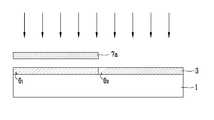
도 1 및 도 2는 멀티도메인의 구현방법을 도시한 것으로, 도 1은 러빙방향을 이용한 멀티도메인 구현방법을 나타낸 것이고, 도 2는 광배향을 이용한 멀티도메인 구현방법을 나타낸 것이다.1 and 2 illustrate a multi-domain implementation method, FIG. 1 illustrates a multi-domain implementation method using a rubbing direction, and FIG. 2 illustrates a multi-domain implementation method using an optical orientation.
먼저, 도 1a에 도시한 바와 같이, 박막트랜지스터 또는 칼라필터와 같은 복수개의 패턴들(도면에 도시하지 않음)이 형성된 기판(1) 위에 배향막(3)을 균일하게 도포한 다음, 회전하는 러빙롤(5)을 이용하여 일방향으로 러빙한다. 러빙공정은 액정분자의 초기 배향방향을 결정해주는 공정이다.First, as shown in FIG. 1A, the
이어서, 도 1b에 도시한 바와 같이, 상기 일방향으로 러빙된 배향막(3)상에 포토레지스트(photo resist)를 도포한 후, 사진식각공정을 통하여 배향막(3)의 일부를 노출시키는 포토레지스트패턴(7)을 형성한다. 이어서, 도 1c에 도시한 바와 같이, 상기 포토레지스트 패턴(7)에 보호되지 않는 배향막(3)이 서로반대방향으로 러빙되도록 러빙롤(5)을 반대방향으로 회전시킨다. 이와같이, 러빙롤의 회전하는 방향에 따라 배향막의 러빙방향이 달라지는 것을 이용함으로써, 각 화소내에 액정의 배향이 서로 다른 다수의 영역을 형성할 수 있다.Subsequently, as shown in FIG. 1B, a photoresist is applied onto the
상기와 같이, 러빙롤을 사용하지 않고, 도 2에 도시된 바와 같이, 상기 선택적으로 블로킹된 마스크(7a)를 사용하여 광배향처리방법(photo-alignment method)으로 자외선을 조사함으로써, 멀티도메인 구조를 형성할 수도 있다.As described above, without using a rubbing roll, as shown in Fig. 2, by irradiating ultraviolet rays with a photo-alignment method using the selectively blocked mask (7a), a multi-domain structure May be formed.
즉, 도 2a에 도시한 바와 같이, 기판(1) 위에 배향막(3)을 균일하게 도포한 다음, 회전하는 러빙롤(5)을 이용하여 일방향으로 러빙하여 제 1프리틸트각(θ1)을 형성한다. 이후, 도 2b에서와 같이 블로킹된 마스크(7a) 상부에서 UV를 조사하여 노출된 배향막(3)에 제 1프리틸트각(θ1) 보다 작은 제 2 프리틸트각(θ2)을 형성한다. 상기와 같은 과정을 반복하여 멀티도메인을 형성할 수 있다.That is, as shown in FIG. 2A, the
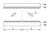
도 3은 하나의 화소에 두개의 도메인을 형성하기 위한 러빙방향(도 3a)과 그에 따른 액정의 배열상태(도 3b)를 나타낸 것이다.3 illustrates a rubbing direction (FIG. 3A) for forming two domains in one pixel and an arrangement state of the liquid crystal (FIG. 3B) accordingly.
먼저, 도 3a에 도시한 바와 같이, 한화소를 제 1영역(A)과 제 2영역(B)으로 나누어 상부기판과 하부기판 각각에 대하여 액정의 배향방향이 서로 반대가 되도록 러빙한다. 도면에서, 실선은 상부기판의 러빙방향을 나타내고, 점선은 하부기판의 러빙방향을 나타낸다.First, as illustrated in FIG. 3A, the Han pixel is divided into a first region A and a second region B, and rubbed so that the alignment directions of the liquid crystals are reversed with respect to the upper and lower substrates, respectively. In the drawing, the solid line indicates the rubbing direction of the upper substrate, and the dotted line indicates the rubbing direction of the lower substrate.
도 3b는 도 3a의 I-I'의 절단면으로, 실질적으로 액정층 안에서 러빙방향에 따라 액정이 배열된 모습을 나타낸 것이다. 도면에 도시한 바와 같이, 상부기판(10a)에 형성된 배향막(13a)과 하부기판(10b)에 형성된 배향막(13b)은 서로 반대방향으로 러빙되어 있기 때문에 이에 따라 액정(15)의 배향방향도 상,하기 판(10a,10b)에 대하여 180°방향이 바뀌어 있다. 또한, A영역과 B영역은 상,하배향막(13a,13b)의 러빙방향이 바뀌는 경계면을 기준으로 하여 액정의 배향방향이 서로 대칭을 이룬다. 따라서, A영역과 B영역에 대하여 액정의 배열방향이 다른 2도메인(two domain)을 형성하게 된다. 이때, 액정의 배열방향이 바뀌는 도메인의 경계영역으로 투과되는 빛은 화면상에 검은줄 또는 힌줄과 같은 디스클리네이션 라인(disclination line)을 나타낸다. 즉, 상기 도메인 경계영역에서는 빛이 액정을 투과하지 않고, 상부기판만을 투과하기 때문에 상하부기판에 부착된 상하편광판의 편광방향이 서로 수직인 경우에는 화면에 검은줄(black line)이 나타내고, 상하부기판에 부착된 상하편광판의 편광방향이 서로 평행인 경우에는 흰줄(white line)을 나타내게 된다. 그러나, 실질적으로, 상부기판의 공통전극과 하부기판의 화소전극에 전압이 인가되면 화면에 표시되는 디스클리네이션 라인은 S자형 곡선을 그리게 된다. 즉, 도 4에 도시한 바와 같이, 화소의 중심부에 도메인 경계를 가지는 액정표시소자의 경우, 해당화소(21b)와 상기 화소(21b)의 좌우에 인접하는 화소들(21a,21c)간에 발생되는 프린지 전계(fringe field)에 의해서 도메인 경계영역에 배치되는 액정(30)의 방향이 바뀌게 된다. 즉, 화소의 에지영역에 배된 액정들이 화소간에 발생되는 프린지 전계(fringe field)의 영향으로 재배열하게 되며, 이때, 재배열된 액정(30)의 경계면 즉, 디스클리네이션 라인(20)은 S자형 곡선을 만들게 된다. 이때, 상기 디스클리네이션 라인(20)의 표시불량(검은줄 또는 흰줄)을 가리기 위하여 이영역에 블랙매트릭스(25)를 형성하게 된다. 그러나, 상기 디스클리네이션 라인(20)은 S자형 곡선을 이루고 있기 때문에 이 부분을 가리기 위하여 블랙매트릭스(25)의 면적이 넓어짐에 따라 개구율이 감소하는 문제점이 있었다.FIG. 3B is a cross-sectional view taken along line II ′ of FIG. 3A, and illustrates a state in which liquid crystals are arranged in a rubbing direction in the liquid crystal layer. As shown in the drawing, since the
따라서, 본 발명은 상기와 같은 문제점을 해결하기 위해서 이루어진 것으로, 화소의 에지영역에 해당하는 도메인 경계부에 적어도 두개 이상의 슬릿 또는 돌출부를 두어 전계를 왜곡시킴으로써, -자 형의 디스클리네이션 라인을 유도하여 블랙매트릭스의 형성영역을 줄여 개구율을 향상시킬 수 있는 멀티도메인 액정표시소자를 제공하는데 그 목적이 있다.Accordingly, the present invention has been made to solve the above problems, by distorting the electric field by placing at least two or more slits or protrusions in the domain boundary corresponding to the edge region of the pixel, to induce a --shaped disclination line An object of the present invention is to provide a multi-domain liquid crystal display device capable of improving the aperture ratio by reducing the formation area of the black matrix.
기타 본 발명의 목적 및 특징은 이하의 발명의 구성 및 특허청구범위에서 상세히 기술될 것이다.Other objects and features of the present invention will be described in detail in the configuration and claims of the following invention.
상기한 목적을 달성하기 위한 본 발명의 멀티도메인 액정표시소자는 제 1 및 제 2기판과; 상기 제 1기판에 종횡으로 배열되어 화소를 정의하는 게이트라인 및 데이터라인과; 상기 제 1 및 제 2기판에 형성되어 한 화소에 대하여 액정배열방향이 서로 다른 두개의 도메인을 형성하는 제 1 및 제 2배향막과; 상기 제 1 및 제 2기판 중 어느 하나의 기판에 형성되고, 상기 두 도메인의 경계에 형성된 전계왜곡수단과; 상기 제 1 및 제 2기판 사이에 형성된 액정층을 포함하여 구성된다.Multi-domain liquid crystal display device of the present invention for achieving the above object and the first and second substrate; Gate lines and data lines arranged vertically and horizontally on the first substrate to define pixels; First and second alignment layers formed on the first and second substrates to form two domains having different liquid crystal alignment directions with respect to one pixel; Field distortion means formed on one of the first and second substrates and formed at a boundary between the two domains; And a liquid crystal layer formed between the first and second substrates.
제 1기판에는 박막트랜지스터 및 화소전극이 형성되어 있으며, 상기 박막트랜지스터는 게이트 전극과, 상기 게이트 전극 위에 형성된 게이트 절연막과, 상기 게이트 절연막 위에 형성된 반도체층과, 상기 반도체층 위에 형성된 소스 전극 및 드레인 전극으로 구성되어 있다.A thin film transistor and a pixel electrode are formed on the first substrate, and the thin film transistor includes a gate electrode, a gate insulating film formed on the gate electrode, a semiconductor layer formed on the gate insulating film, a source electrode and a drain electrode formed on the semiconductor layer. It consists of.
제 2기판에는 칼라필터, 블랙매트릭스 및 공통전극이 형성되어 있으며, 상기 블랙매트릭스는 상기 두 도메인의 경계에 형성되어 화면상에 검은줄 또는 흰줄을 표시하는 디스클리네이션 라인을 가려준다. The second substrate is formed with a color filter, a black matrix and a common electrode, and the black matrix is formed at the boundary between the two domains to cover the disclination line displaying black or white lines on the screen.
또한, 상기 전계왜곡수단은 제 1기판 또는 제 2기판 중 어느 하나에 형성되며, 제 1기판과 제 2기판 사이에 생기는 수직전계를 왜곡시킴으로써, 도메인 경계에서 발생되는 디스클리네이션 라인을 -자 형태로 보정해주는 역할을 한다. 이때, 전계왜곡수단은 슬릿 또는 돌기로 형성할 수 있다.In addition, the electric field distortion means is formed on any one of the first substrate or the second substrate, and by distorting the vertical electric field generated between the first substrate and the second substrate, the shape of the disc-cleaning line generated at the domain boundary- It serves as a correction. In this case, the electric field distortion means may be formed of slits or protrusions.
이하, 첨부한 도면을 통하여 본 발명에 따른 멀티도메인 액정표시소자 및 그 제조방법에 대하여 상세히 설명한다.Hereinafter, a multi-domain liquid crystal display device and a manufacturing method thereof according to the present invention will be described in detail with reference to the accompanying drawings.
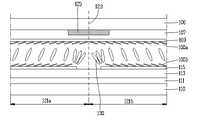
도 5는 본 발명의 실시예에 따른 멀티도메인 액정표시소자를 나타낸 도면으로, 도 5a는 전계왜곡수단으로써 화소영역의 중심에 -자형태의 슬릿이 구비된 단위화소를 개략적으로 나타낸 평면도이고, 도 5b는 도 5a의 II-II' 절단선에 따른 액정표시소자의 단면도이다.FIG. 5 is a diagram illustrating a multi-domain liquid crystal display device according to an exemplary embodiment of the present invention. FIG. 5A is a plan view schematically illustrating a unit pixel having a -shaped slit at the center of a pixel region as an electric field distortion means. 5B is a cross-sectional view of the liquid crystal display device taken along the line II-II ′ of FIG. 5A.
도면에 도시한 바와 같이, 본 발명의 실시예에 따른 멀티도메인 액정표시소자는 종횡으로 배열된 게이트라인(101)과 데이터라인(102)에 의해서 화소(121)가 정의되며, 상기 화소(121)에는 중심부에 도메인 경계를 형성하는 2도메인 구조를 가진다. 그리고, 상기 게이트라인(101)과 데이터라인(102)의 교차부에는 박막트랜지스터(T)가 배치되어 있으며, 상기 박막트랜지스터(T)는 게이트라인(101)으로부터 인출된 게이트전극(101a)과, 상기 게이트전극(101a) 상에 형성된 반도체층(105)과 상기 반도체층(105) 상에 형성된 소스/드레인전극(102a,102b)으로 구성된다.As shown in the figure, in the multi-domain liquid crystal display according to the exemplary embodiment of the present invention, the
2도메인 구조는 배향막의 배향처리에 의해서 액정의 배열방향이 서로 다른 제 1영역(121a)과 제 2영역(121b)을 형성하게 된다. 그리고, 화소(121)의 에지영역을 제외한 그 중심부에는 상부기판(100) 및 하부기판(110) 사이에 발생되는 전계를 왜곡시키기 위한 전계왜곡수단으로써 -자 형태의 슬릿(120)이 구비되어 있다. 또한, 화소(121)의 중심부에는 디스클리네이션 라인(123)을 가리기 위해 형성된 블랙매트릭스(125)가 배치되어 있다.In the two-domain structure, the
상부기판(100)에는 칼라를 구현하기 위한 칼라필터(107) 및 빛샘방지를 위한 블랙매트릭스(125)가 형성되어 있다. 도면에는 디스클리네이션 라인(123)을 가려주기 위한 목적으로 형성된 블랙매트릭스(125)만을 도시하였으나, 실질적으로 게이트라인(101), 데이터라인(102) 및 박막트랜지스터(T) 영역에도 형성된다. 또한, 상기 칼라필터(107) 위에는 액정(130)에 전계를 인가해주는 공통전극(109)이 형성되어 있다.The
하부기판(110)에는 게이트절연막(111)과 보호막(113)이 적층되어 있으며, 도면에 상세하게 도시하진 않았지만, 상기 게이트절연막(111)은 게이트라인(101)과 데이터라인(102)을 절연시키며, 보호막(113)은 박막트랜지스터(T)위에 형성되어 이를 보호한다. 또한, 상기 보호막(113) 상에는 공통전극(109)과 함께 액정층에 수직전계를 발생시키는 화소전극(115)이 형성되어 있다. 그리고, 상부기판(100)과 하부기판(110)의 대향면에는 2도메인구조를 형성하는 상하부배향막(100a,100b)이 형성되어 있으며, 상기 배항막(100a,100b)의 러빙방향에 따라 액정의 초기 배열상태가 결정된다.A
또한, 도메인 경계면에 대응하는 하부기판(110)에는 슬릿(120)이 형성되어 있으며, 상기 슬릿(120)은 상부기판(100)과 하부기판(110) 사이에 형성되는 수직전계를 왜곡시키고, 도메인 경계 근처에 배열된 액정(130)이 슬릿(120)에 의해서 왜곡된 전계를 따라 배열되도록 한다. 이때, 슬릿(120)에 의해서 재배열된 액정(130)은 -자 형태의 디스클리네이션 라인(123)을 유도하게 된다. 즉, 종래기술에 언급한 바와 같이, 인접하는 화소들 간에 발생되는 프린지 전계는 도메인 경계영역에 배열된 액정을 왜곡시켜 화면상에 S자형 곡선의 디스클리네이션 라인을 발생시키게 된다(도 3참조). 그러나, 본 실시예와 같이 도메인 경계영역에 슬릿(120)을 형성하게 되면, 상기 슬릿(120)에 의해 왜곡된 전계는 상기 프린지 전계의 영향을 최소화하여 액정의 도메인 경계 즉, 디스클리네이션 라인(123)이 휘는 것을 막아준다.In addition, a
따라서, 종래 곡선형태의 디스클리네이션 라인을 -자 형태로 유도함으로써, 디스클리네이션 라인(123)을 가려주는 블랙매트릭스(125)의 면적을 줄일 수가 있다. 그러나, 상기한 구조(도 5)에서도 슬릿(120)이 형성되지 않은 화소(121)의 에지영역에서는 여전히 프린지 전계의 영향으로 인하여 디스클리네이션 라인(123)이 휘어지게 된다. 따라서, 블랙매트릭스(125)의 면적을 줄여 개구율을 향상시키는데 한계가 있었다.Therefore, the area of the
도 6내지 도 7은 블랙매트릭스의 형성영역을 줄여 개구율을 향상시킬 수 있는 본 발명의 다른 실시예를 나타낸 도면으로, 본 발명의 다른 실시예는 슬릿의 형태를 제외한 모든 구성요소가 앞서 도시된 도면(도 4)에서와 동일하다. 따라서, 그 차이점만을 설명하기로 한다.6 to 7 is a view showing another embodiment of the present invention that can improve the aperture ratio by reducing the formation area of the black matrix, another embodiment of the present invention is a view showing all the components except the shape of the slit previously Same as in (Fig. 4). Therefore, only the differences will be described.
도면에 도시한 바와 같이, 본 발명의 다른 실시예에 따른 멀티도메인 액정표시소자는 화소(221)의 양쪽 에지영역 도메인의 경계영역에 -자 형태의 슬릿(220, 320)이 형성되어 있으며, 상기 슬릿(220)은 화소의 에지영역에서 디스클리네이션 라인(223)의 직선 형태를 유도한다. 즉, 인접하는 화소에 의해서 화소의 에지영역에 작용하는 프린지 전계의 영향을 최소화하여 디스클리네이션 라인이 휘는 것을 막을 수 있다. 따라서, 상기 디스클리네이션 라인(223)을 가리기 위한 블랙매트릭스(225)의 면적을 줄일 수가 있으며, 이에 따라 개구율을 더욱 향상시킬 수가 있다.As shown in the figure, in the multi-domain liquid crystal display device according to another exemplary embodiment of the present invention, slits 220 and 320 having a “-shape” are formed at boundary regions of both edge region domains of the
슬릿은 도 6에 도시한 바와 같이, 화소의 양쪽 에지영역에 두개로 형성할 수 있으며, 도 7에 도시한 바와 같이, 화소의 에지영역 및 중심부에 3개로 형성할 수 있다.As illustrated in FIG. 6, two slits may be formed in both edge regions of the pixel, and as illustrated in FIG. 7, three slits may be formed in the edge region and the central portion of the pixel.
슬릿은 상부기판 또는 하부기판에 형성될 수 있으며, 상부기판에 슬릿을 형성하는 경우에는 도메인 경계를 모두 슬릿으로 둘 수도 있다. 즉, 상부기판에는 공통전극이 기판 전체에 걸쳐서 형성되어 있기 때문에 한화소에 대하여 도메인 경계를 모두 슬릿으로 형성하는 것이 가능하다. 그러나, 하부기판에 화소영역에만 화소전극이 형성되어 있기 때문에 도메인 경계부에 슬릿을 형성하되, 슬릿에 의해서 분리되는 화소들 간에 적어도 하나이상의 연결부를 두어야 한다.The slits may be formed on the upper substrate or the lower substrate. When the slits are formed on the upper substrate, all of the domain boundaries may be formed as slits. That is, since the common electrode is formed on the entire substrate on the upper substrate, it is possible to form all the domain boundaries with one slit for the one pixel. However, since the pixel electrode is formed only in the pixel region on the lower substrate, a slit is formed at the domain boundary, and at least one connection portion must be provided between the pixels separated by the slit.
상기 슬릿은 도메인 경계부에 형성되는 디스클리네이션 라인을 -자형태로 유도하기 위한 전계왜곡수단으로, 슬릿대신에 돌기를 형성할 수도 있다. 돌기를 형성하는 경우에도, 슬릿을 형성하는 경우와 동일한 효과를 볼 수 있으며, 상부기판 또 는 하부기판에 형성하는 것이 모두 가능하다.The slit is an electric field distortion means for guiding the disclination line formed at the domain boundary in the form of-, and may form a protrusion instead of the slit. Even when forming the projections, the same effects as in the case of forming the slit can be seen, it is possible to form both on the upper substrate or the lower substrate.
도 8은 본 발명의 또다른 실시예로써, 하부기판에 돌기가 형성된 멀티도메인 액정표시소자의 단면도를 나타낸 것이다. 돌기를 제외한 모든 구성요소들은 이전 도면과 동일하다.8 is a cross-sectional view of a multi-domain liquid crystal display device having protrusions formed on a lower substrate according to another embodiment of the present invention. All components except protrusions are the same as in the previous drawings.
도면에 도시한 바와 같이, 화소전극(115)을 포함하는 하부기판(110)에는 도메인 경계를 따라서 돌기(420)가 형성되어 있다. 상기 돌기(420)는 슬릿과 마찬가지로 상부기판(100)에 형성된 공통전극(109)과 하부기판(110)에 형성된 화소전극(115)에 의해서 발생되는 수직전계를 왜곡시키며, 도메인 경계 근처에 배열된 액정(130)이 돌기(420)에 의해서 왜곡된 전계를 따라 배열되도록 한다. 이때, 슬릿(120)에 의해서 재배열된 액정(130)은 도메인의 경계부에 -자 형태의 디스클리네이션 라인을 유도하게 된다. 상기와 같이, 도메인 경계에 돌기(420)를 형성하게 되면, 2도메인을 형성하는 상부 및 하부 배향막(400a,400b)의 러빙방향도 슬릿인 경우와 반대로 바꾸어주어야 한다. 상기와 같이, 디스클리네이션 라인이 -자 형태로 유도됨에 따라, 디스클리네이션 라인을 가리기 위해 상부기판(100)에 형성되는 블랙매트릭스(425)의 크기도 줄일 수가 있다. 블랙매트릭스(425)가 형성되는 면적이 줄어들게되면, 그만큼의 개구율을 향상시킬 수가 있다.As shown in the figure,
상술한 바와 같이, 본 발명은 배향막의 러빙방향을 다르게 하여 2도메인을 형성하고, 도메인의 경계면에 슬릿 또는 돌기를 형성하여 디스클리네이션 라인을 직선형태로 바꾸어줌으로써, 블랙매트릭스 형성영역을 줄여 개구율을 향상시킬 수 있다.As described above, the present invention forms two domains by varying the rubbing direction of the alignment layer, and forms a slit or a protrusion at the interface of the domain to change the disclination line into a straight line, thereby reducing the black matrix formation region to reduce the aperture ratio. Can be improved.
Claims (9)
Translated fromKoreanPriority Applications (2)
| Application Number | Priority Date | Filing Date | Title |
|---|---|---|---|
| KR1020020088454AKR100945372B1 (en) | 2002-12-31 | 2002-12-31 | Multi-domain liquid crystal display device |
| US10/713,192US7251002B2 (en) | 2002-12-31 | 2003-11-17 | Multi-domain liquid crystal display device having particular electric field distorting means |
Applications Claiming Priority (1)
| Application Number | Priority Date | Filing Date | Title |
|---|---|---|---|
| KR1020020088454AKR100945372B1 (en) | 2002-12-31 | 2002-12-31 | Multi-domain liquid crystal display device |
Publications (2)
| Publication Number | Publication Date |
|---|---|
| KR20040062128A KR20040062128A (en) | 2004-07-07 |
| KR100945372B1true KR100945372B1 (en) | 2010-03-08 |
Family
ID=32653283
Family Applications (1)
| Application Number | Title | Priority Date | Filing Date |
|---|---|---|---|
| KR1020020088454AExpired - Fee RelatedKR100945372B1 (en) | 2002-12-31 | 2002-12-31 | Multi-domain liquid crystal display device |
Country Status (2)
| Country | Link |
|---|---|
| US (1) | US7251002B2 (en) |
| KR (1) | KR100945372B1 (en) |
Families Citing this family (6)
| Publication number | Priority date | Publication date | Assignee | Title |
|---|---|---|---|---|
| US7480022B2 (en)* | 2003-12-10 | 2009-01-20 | Seiko Epson Corporation | Liquid crystal display device, method of manufacturing liquid crystal display device, and electronic apparatus |
| KR101442147B1 (en)* | 2008-01-30 | 2014-11-03 | 삼성디스플레이 주식회사 | Liquid crystal display |
| WO2010070772A1 (en)* | 2008-12-19 | 2010-06-24 | 株式会社有沢製作所 | Liquid crystal filter, phase difference plate, and optical low pass filter |
| KR20100071141A (en)* | 2008-12-19 | 2010-06-29 | 삼성전자주식회사 | Display substrate, liquid crystal display device having the display substrate and method of manufacturing the display substrate |
| KR101973061B1 (en)* | 2012-02-27 | 2019-04-29 | 삼성디스플레이 주식회사 | Display substrate, display panel having the same, method of manufacturing the same and method of manufacturing the display panel |
| US11754875B2 (en)* | 2021-05-14 | 2023-09-12 | Sharp Kabushiki Kaisha | Liquid crystal display panel and 3D display device |
Citations (4)
| Publication number | Priority date | Publication date | Assignee | Title |
|---|---|---|---|---|
| KR20000040118A (en)* | 1998-12-17 | 2000-07-05 | 김영환 | Vertical alignment mode liquid crystal display device |
| KR20010069132A (en)* | 2000-01-12 | 2001-07-23 | 구본준, 론 위라하디락사 | Multi-domain liquid crystal display device |
| JP2001235748A (en) | 2000-02-23 | 2001-08-31 | Fujitsu Ltd | Multi-domain liquid crystal display |
| KR20020031454A (en)* | 2000-10-20 | 2002-05-02 | 구본준, 론 위라하디락사 | Multidomain liquid crystal display and method for fabricating it |
Family Cites Families (17)
| Publication number | Priority date | Publication date | Assignee | Title |
|---|---|---|---|---|
| JP2903833B2 (en) | 1992-02-18 | 1999-06-14 | 日本電気株式会社 | Liquid crystal display |
| JP3175972B2 (en) | 1992-03-31 | 2001-06-11 | 株式会社東芝 | Liquid crystal display |
| JP3043211B2 (en) | 1993-12-03 | 2000-05-22 | 富士通株式会社 | Liquid crystal display |
| US5781262A (en)* | 1994-04-19 | 1998-07-14 | Nec Corporation | Liquid crystal display cell |
| JP2624197B2 (en) | 1994-04-19 | 1997-06-25 | 日本電気株式会社 | Liquid crystal display |
| DE19542981A1 (en)* | 1994-11-17 | 1996-05-23 | Nec Corp | Twisted nematic liquid crystal display device |
| JP2734444B2 (en)* | 1996-03-22 | 1998-03-30 | 日本電気株式会社 | Liquid crystal display |
| JPH09281497A (en) | 1996-04-11 | 1997-10-31 | Toshiba Corp | Liquid crystal display |
| JP3617719B2 (en)* | 1996-04-15 | 2005-02-09 | 株式会社東芝 | Liquid crystal display |
| JP2880985B2 (en) | 1997-10-30 | 1999-04-12 | 株式会社ソフィア | Ball game machine |
| KR100309918B1 (en)* | 1998-05-16 | 2001-12-17 | 윤종용 | Liquid crystal display having wide viewing angle and method for manufacturing the same |
| KR100354904B1 (en)* | 1998-05-19 | 2002-12-26 | 삼성전자 주식회사 | Wide viewing angle liquid crystal display device |
| US6335776B1 (en)* | 1998-05-30 | 2002-01-01 | Lg. Philips Lcd Co., Ltd. | Multi-domain liquid crystal display device having an auxiliary electrode formed on the same layer as the pixel electrode |
| JP2000010119A (en)* | 1998-06-23 | 2000-01-14 | Mitsubishi Electric Corp | Liquid crystal display device and method of manufacturing array substrate used in the device |
| KR100357213B1 (en)* | 1998-07-23 | 2002-10-18 | 엘지.필립스 엘시디 주식회사 | Multi-domain liquid crystal display device |
| KR100313952B1 (en)* | 1998-08-20 | 2002-11-23 | 엘지.필립스 엘시디 주식회사 | Multi-domain liquid crystal display device |
| TWI271573B (en)* | 2001-08-22 | 2007-01-21 | Advanced Display Kk | Liquid crystal display device and method of producing the same |
- 2002
- 2002-12-31KRKR1020020088454Apatent/KR100945372B1/ennot_activeExpired - Fee Related
- 2003
- 2003-11-17USUS10/713,192patent/US7251002B2/ennot_activeExpired - Lifetime
Patent Citations (4)
| Publication number | Priority date | Publication date | Assignee | Title |
|---|---|---|---|---|
| KR20000040118A (en)* | 1998-12-17 | 2000-07-05 | 김영환 | Vertical alignment mode liquid crystal display device |
| KR20010069132A (en)* | 2000-01-12 | 2001-07-23 | 구본준, 론 위라하디락사 | Multi-domain liquid crystal display device |
| JP2001235748A (en) | 2000-02-23 | 2001-08-31 | Fujitsu Ltd | Multi-domain liquid crystal display |
| KR20020031454A (en)* | 2000-10-20 | 2002-05-02 | 구본준, 론 위라하디락사 | Multidomain liquid crystal display and method for fabricating it |
Also Published As
| Publication number | Publication date |
|---|---|
| KR20040062128A (en) | 2004-07-07 |
| US7251002B2 (en) | 2007-07-31 |
| US20040125297A1 (en) | 2004-07-01 |
Similar Documents
| Publication | Publication Date | Title |
|---|---|---|
| CN102566125B (en) | Liquid crystal display device | |
| KR100251878B1 (en) | Liquid crystal display | |
| US6067140A (en) | Liquid crystal display device and method of manufacturing same | |
| US6297866B1 (en) | In-plane switching mode liquid crystal display device | |
| EP2105786B1 (en) | Liquid crystal display | |
| JP3680730B2 (en) | Liquid crystal display | |
| US20040125295A1 (en) | Liquid crystal display device and a method of manufacturing a viewing angle compensation film for the same | |
| US8149361B2 (en) | Liquid crystal display | |
| JP4202062B2 (en) | Liquid crystal display | |
| JP4541815B2 (en) | Transflective liquid crystal display device and manufacturing method thereof | |
| KR102340226B1 (en) | Liquid crystal display and manufacturing method thereof | |
| KR101635954B1 (en) | Liquid crystal display | |
| JP6684092B2 (en) | Curved liquid crystal display | |
| KR100945372B1 (en) | Multi-domain liquid crystal display device | |
| JP3796115B2 (en) | Liquid crystal display | |
| US6630971B1 (en) | Multi-domain liquid crystal display device | |
| JP3500547B2 (en) | Method of manufacturing liquid crystal display panel and liquid crystal display panel | |
| US7808593B1 (en) | Multi-domain liquid crystal display | |
| KR100244537B1 (en) | A liquid crystal display device | |
| JP2004163746A (en) | Liquid crystal display | |
| KR100313948B1 (en) | Multi-domain liquid crystal display device | |
| KR20030033833A (en) | Multi-domain Liquid Crystal Display Device And Method For Fabricating The Same | |
| KR100662490B1 (en) | Multi-domain liquid crystal display device and manufacturing method thereof | |
| JP3879902B2 (en) | Liquid crystal display | |
| JPH09171175A (en) | Liquid crystal display device |
Legal Events
| Date | Code | Title | Description |
|---|---|---|---|
| PA0109 | Patent application | St.27 status event code:A-0-1-A10-A12-nap-PA0109 | |
| PG1501 | Laying open of application | St.27 status event code:A-1-1-Q10-Q12-nap-PG1501 | |
| A201 | Request for examination | ||
| PA0201 | Request for examination | St.27 status event code:A-1-2-D10-D11-exm-PA0201 | |
| PN2301 | Change of applicant | St.27 status event code:A-3-3-R10-R13-asn-PN2301 St.27 status event code:A-3-3-R10-R11-asn-PN2301 | |
| D13-X000 | Search requested | St.27 status event code:A-1-2-D10-D13-srh-X000 | |
| D14-X000 | Search report completed | St.27 status event code:A-1-2-D10-D14-srh-X000 | |
| E902 | Notification of reason for refusal | ||
| PE0902 | Notice of grounds for rejection | St.27 status event code:A-1-2-D10-D21-exm-PE0902 | |
| P11-X000 | Amendment of application requested | St.27 status event code:A-2-2-P10-P11-nap-X000 | |
| P13-X000 | Application amended | St.27 status event code:A-2-2-P10-P13-nap-X000 | |
| E902 | Notification of reason for refusal | ||
| PE0902 | Notice of grounds for rejection | St.27 status event code:A-1-2-D10-D21-exm-PE0902 | |
| E13-X000 | Pre-grant limitation requested | St.27 status event code:A-2-3-E10-E13-lim-X000 | |
| P11-X000 | Amendment of application requested | St.27 status event code:A-2-2-P10-P11-nap-X000 | |
| P13-X000 | Application amended | St.27 status event code:A-2-2-P10-P13-nap-X000 | |
| E701 | Decision to grant or registration of patent right | ||
| PE0701 | Decision of registration | St.27 status event code:A-1-2-D10-D22-exm-PE0701 | |
| GRNT | Written decision to grant | ||
| PR0701 | Registration of establishment | St.27 status event code:A-2-4-F10-F11-exm-PR0701 | |
| PR1002 | Payment of registration fee | St.27 status event code:A-2-2-U10-U11-oth-PR1002 Fee payment year number:1 | |
| PG1601 | Publication of registration | St.27 status event code:A-4-4-Q10-Q13-nap-PG1601 | |
| R18-X000 | Changes to party contact information recorded | St.27 status event code:A-5-5-R10-R18-oth-X000 | |
| R18-X000 | Changes to party contact information recorded | St.27 status event code:A-5-5-R10-R18-oth-X000 | |
| R18-X000 | Changes to party contact information recorded | St.27 status event code:A-5-5-R10-R18-oth-X000 | |
| FPAY | Annual fee payment | Payment date:20121228 Year of fee payment:4 | |
| PR1001 | Payment of annual fee | St.27 status event code:A-4-4-U10-U11-oth-PR1001 Fee payment year number:4 | |
| FPAY | Annual fee payment | Payment date:20131227 Year of fee payment:5 | |
| PR1001 | Payment of annual fee | St.27 status event code:A-4-4-U10-U11-oth-PR1001 Fee payment year number:5 | |
| FPAY | Annual fee payment | Payment date:20150127 Year of fee payment:6 | |
| PR1001 | Payment of annual fee | St.27 status event code:A-4-4-U10-U11-oth-PR1001 Fee payment year number:6 | |
| FPAY | Annual fee payment | Payment date:20160128 Year of fee payment:7 | |
| PR1001 | Payment of annual fee | St.27 status event code:A-4-4-U10-U11-oth-PR1001 Fee payment year number:7 | |
| FPAY | Annual fee payment | Payment date:20170116 Year of fee payment:8 | |
| PR1001 | Payment of annual fee | St.27 status event code:A-4-4-U10-U11-oth-PR1001 Fee payment year number:8 | |
| PR1001 | Payment of annual fee | St.27 status event code:A-4-4-U10-U11-oth-PR1001 Fee payment year number:9 | |
| LAPS | Lapse due to unpaid annual fee | ||
| PC1903 | Unpaid annual fee | St.27 status event code:A-4-4-U10-U13-oth-PC1903 Not in force date:20190225 Payment event data comment text:Termination Category : DEFAULT_OF_REGISTRATION_FEE | |
| PC1903 | Unpaid annual fee | St.27 status event code:N-4-6-H10-H13-oth-PC1903 Ip right cessation event data comment text:Termination Category : DEFAULT_OF_REGISTRATION_FEE Not in force date:20190225 |