KR100941065B1 - Bio Lab-on-a-Chip, and Method of Manufacturing and Operating the Same - Google Patents
Bio Lab-on-a-Chip, and Method of Manufacturing and Operating the SameDownload PDFInfo
- Publication number
- KR100941065B1 KR100941065B1KR1020070114116AKR20070114116AKR100941065B1KR 100941065 B1KR100941065 B1KR 100941065B1KR 1020070114116 AKR1020070114116 AKR 1020070114116AKR 20070114116 AKR20070114116 AKR 20070114116AKR 100941065 B1KR100941065 B1KR 100941065B1
- Authority
- KR
- South Korea
- Prior art keywords
- sensing
- bio
- chip
- thin film
- piezoelectric thin
- Prior art date
- Legal status (The legal status is an assumption and is not a legal conclusion. Google has not performed a legal analysis and makes no representation as to the accuracy of the status listed.)
- Expired - Fee Related
Links
Images


Classifications
- G—PHYSICS
- G01—MEASURING; TESTING
- G01N—INVESTIGATING OR ANALYSING MATERIALS BY DETERMINING THEIR CHEMICAL OR PHYSICAL PROPERTIES
- G01N33/00—Investigating or analysing materials by specific methods not covered by groups G01N1/00 - G01N31/00
- G01N33/48—Biological material, e.g. blood, urine; Haemocytometers
- G01N33/50—Chemical analysis of biological material, e.g. blood, urine; Testing involving biospecific ligand binding methods; Immunological testing
- G01N33/53—Immunoassay; Biospecific binding assay; Materials therefor
- G01N33/543—Immunoassay; Biospecific binding assay; Materials therefor with an insoluble carrier for immobilising immunochemicals
- G01N33/54366—Apparatus specially adapted for solid-phase testing
- B—PERFORMING OPERATIONS; TRANSPORTING
- B01—PHYSICAL OR CHEMICAL PROCESSES OR APPARATUS IN GENERAL
- B01L—CHEMICAL OR PHYSICAL LABORATORY APPARATUS FOR GENERAL USE
- B01L3/00—Containers or dishes for laboratory use, e.g. laboratory glassware; Droppers
- B01L3/50—Containers for the purpose of retaining a material to be analysed, e.g. test tubes
- B01L3/502—Containers for the purpose of retaining a material to be analysed, e.g. test tubes with fluid transport, e.g. in multi-compartment structures
- B01L3/5027—Containers for the purpose of retaining a material to be analysed, e.g. test tubes with fluid transport, e.g. in multi-compartment structures by integrated microfluidic structures, i.e. dimensions of channels and chambers are such that surface tension forces are important, e.g. lab-on-a-chip
- B01L3/502707—Containers for the purpose of retaining a material to be analysed, e.g. test tubes with fluid transport, e.g. in multi-compartment structures by integrated microfluidic structures, i.e. dimensions of channels and chambers are such that surface tension forces are important, e.g. lab-on-a-chip characterised by the manufacture of the container or its components
- B—PERFORMING OPERATIONS; TRANSPORTING
- B01—PHYSICAL OR CHEMICAL PROCESSES OR APPARATUS IN GENERAL
- B01L—CHEMICAL OR PHYSICAL LABORATORY APPARATUS FOR GENERAL USE
- B01L3/00—Containers or dishes for laboratory use, e.g. laboratory glassware; Droppers
- B01L3/50—Containers for the purpose of retaining a material to be analysed, e.g. test tubes
- B01L3/502—Containers for the purpose of retaining a material to be analysed, e.g. test tubes with fluid transport, e.g. in multi-compartment structures
- B01L3/5027—Containers for the purpose of retaining a material to be analysed, e.g. test tubes with fluid transport, e.g. in multi-compartment structures by integrated microfluidic structures, i.e. dimensions of channels and chambers are such that surface tension forces are important, e.g. lab-on-a-chip
- B01L3/50273—Containers for the purpose of retaining a material to be analysed, e.g. test tubes with fluid transport, e.g. in multi-compartment structures by integrated microfluidic structures, i.e. dimensions of channels and chambers are such that surface tension forces are important, e.g. lab-on-a-chip characterised by the means or forces applied to move the fluids
- G—PHYSICS
- G01—MEASURING; TESTING
- G01N—INVESTIGATING OR ANALYSING MATERIALS BY DETERMINING THEIR CHEMICAL OR PHYSICAL PROPERTIES
- G01N33/00—Investigating or analysing materials by specific methods not covered by groups G01N1/00 - G01N31/00
- G01N33/48—Biological material, e.g. blood, urine; Haemocytometers
- G01N33/50—Chemical analysis of biological material, e.g. blood, urine; Testing involving biospecific ligand binding methods; Immunological testing
- G01N33/53—Immunoassay; Biospecific binding assay; Materials therefor
- G01N33/543—Immunoassay; Biospecific binding assay; Materials therefor with an insoluble carrier for immobilising immunochemicals
- G01N33/54366—Apparatus specially adapted for solid-phase testing
- G01N33/54373—Apparatus specially adapted for solid-phase testing involving physiochemical end-point determination, e.g. wave-guides, FETS, gratings
- G01N33/5438—Electrodes
- B—PERFORMING OPERATIONS; TRANSPORTING
- B01—PHYSICAL OR CHEMICAL PROCESSES OR APPARATUS IN GENERAL
- B01L—CHEMICAL OR PHYSICAL LABORATORY APPARATUS FOR GENERAL USE
- B01L2200/00—Solutions for specific problems relating to chemical or physical laboratory apparatus
- B01L2200/06—Fluid handling related problems
- B01L2200/0673—Handling of plugs of fluid surrounded by immiscible fluid
- B—PERFORMING OPERATIONS; TRANSPORTING
- B01—PHYSICAL OR CHEMICAL PROCESSES OR APPARATUS IN GENERAL
- B01L—CHEMICAL OR PHYSICAL LABORATORY APPARATUS FOR GENERAL USE
- B01L2300/00—Additional constructional details
- B01L2300/06—Auxiliary integrated devices, integrated components
- B01L2300/0627—Sensor or part of a sensor is integrated
- B01L2300/0636—Integrated biosensor, microarrays
- B—PERFORMING OPERATIONS; TRANSPORTING
- B01—PHYSICAL OR CHEMICAL PROCESSES OR APPARATUS IN GENERAL
- B01L—CHEMICAL OR PHYSICAL LABORATORY APPARATUS FOR GENERAL USE
- B01L2300/00—Additional constructional details
- B01L2300/06—Auxiliary integrated devices, integrated components
- B01L2300/0627—Sensor or part of a sensor is integrated
- B01L2300/0645—Electrodes
- B—PERFORMING OPERATIONS; TRANSPORTING
- B01—PHYSICAL OR CHEMICAL PROCESSES OR APPARATUS IN GENERAL
- B01L—CHEMICAL OR PHYSICAL LABORATORY APPARATUS FOR GENERAL USE
- B01L2300/00—Additional constructional details
- B01L2300/08—Geometry, shape and general structure
- B01L2300/0809—Geometry, shape and general structure rectangular shaped
- B01L2300/0816—Cards, e.g. flat sample carriers usually with flow in two horizontal directions
- B—PERFORMING OPERATIONS; TRANSPORTING
- B01—PHYSICAL OR CHEMICAL PROCESSES OR APPARATUS IN GENERAL
- B01L—CHEMICAL OR PHYSICAL LABORATORY APPARATUS FOR GENERAL USE
- B01L2300/00—Additional constructional details
- B01L2300/08—Geometry, shape and general structure
- B01L2300/089—Virtual walls for guiding liquids
- B—PERFORMING OPERATIONS; TRANSPORTING
- B01—PHYSICAL OR CHEMICAL PROCESSES OR APPARATUS IN GENERAL
- B01L—CHEMICAL OR PHYSICAL LABORATORY APPARATUS FOR GENERAL USE
- B01L2300/00—Additional constructional details
- B01L2300/16—Surface properties and coatings
- B01L2300/161—Control and use of surface tension forces, e.g. hydrophobic, hydrophilic
- B—PERFORMING OPERATIONS; TRANSPORTING
- B01—PHYSICAL OR CHEMICAL PROCESSES OR APPARATUS IN GENERAL
- B01L—CHEMICAL OR PHYSICAL LABORATORY APPARATUS FOR GENERAL USE
- B01L2400/00—Moving or stopping fluids
- B01L2400/04—Moving fluids with specific forces or mechanical means
- B01L2400/0403—Moving fluids with specific forces or mechanical means specific forces
- B01L2400/0433—Moving fluids with specific forces or mechanical means specific forces vibrational forces
- B01L2400/0436—Moving fluids with specific forces or mechanical means specific forces vibrational forces acoustic forces, e.g. surface acoustic waves [SAW]
- B—PERFORMING OPERATIONS; TRANSPORTING
- B01—PHYSICAL OR CHEMICAL PROCESSES OR APPARATUS IN GENERAL
- B01L—CHEMICAL OR PHYSICAL LABORATORY APPARATUS FOR GENERAL USE
- B01L2400/00—Moving or stopping fluids
- B01L2400/04—Moving fluids with specific forces or mechanical means
- B01L2400/0493—Specific techniques used
- B01L2400/0496—Travelling waves, e.g. in combination with electrical or acoustic forces
Landscapes
- Health & Medical Sciences (AREA)
- Chemical & Material Sciences (AREA)
- Immunology (AREA)
- Life Sciences & Earth Sciences (AREA)
- Engineering & Computer Science (AREA)
- Hematology (AREA)
- Biomedical Technology (AREA)
- General Health & Medical Sciences (AREA)
- Analytical Chemistry (AREA)
- Molecular Biology (AREA)
- Urology & Nephrology (AREA)
- Food Science & Technology (AREA)
- General Physics & Mathematics (AREA)
- Medicinal Chemistry (AREA)
- Physics & Mathematics (AREA)
- Cell Biology (AREA)
- Biochemistry (AREA)
- Biotechnology (AREA)
- Microbiology (AREA)
- Pathology (AREA)
- Dispersion Chemistry (AREA)
- Clinical Laboratory Science (AREA)
- Chemical Kinetics & Catalysis (AREA)
- Apparatus Associated With Microorganisms And Enzymes (AREA)
- Investigating Or Analyzing Materials By The Use Of Ultrasonic Waves (AREA)
- Investigating Or Analysing Materials By Optical Means (AREA)
Abstract
Translated fromKorean
Description
Translated fromKorean본 발명은 바이오 미세 전자기계 시스템 및 그 제조 방법에 관한 것으로, 더 구체적으로 바이오 랩온어칩, 및 그 제조 및 작동 방법에 관한 것이다.The present invention relates to a biomicroelectromechanical system and a method for manufacturing the same, and more particularly, to a bio lab-on-a-chip and a method for manufacturing and operating the same.
본 발명은 정보통신부 및 정보통신연구진흥원의 IT원천기술개발사업의 일환으로 수행한 연구로부터 도출된 것이다[과제관리번호: 2006-S-007-02, 과제명: 유비쿼터스 건강관리용 모듈 시스템].The present invention is derived from a study performed as part of the IT source technology development project of the Ministry of Information and Communication and the Ministry of Information and Communication Research and Development [Task Management No .: 2006-S-007-02, Task Name: Ubiquitous Health Management Module System].
일반적으로 바이오 미세 전자기계 시스템(Bio-Micro Electro Mechanical Systems : Bio-MEMS) 분야에서, 질병의 조기 진단 또는/및 화학 분석 등과 같은 과정을 작은 칩(chip) 상에서 수행하기 위해서는 가능한 한 초미량의 유체를 이송, 정지, 혼합 및 반응시킬 수 있는 미세 유체 제어와 질병에 관련된 바이오마커(biomarker, 예를 들어, 단백질, 디엔에이(DeoxyriboNucleic Acid : DNA) 등)를 고감도로 감지하는 센서가 집적되는 것이 반드시 요구된다.In general, in the field of Bio-Micro Electro Mechanical Systems (BIO-MEMS), the smallest amount of fluid possible to carry out processes such as early diagnosis and / or chemical analysis of diseases on a small chip. Microfluidic control capable of transporting, stopping, mixing, and reacting to and integrating sensors with high sensitivity for detecting biomarkers (e.g. proteins, DeoxyriboNucleic Acid, DNA, etc.) do.
바이오 미세 전자기계 시스템 분야에서, 특히 화학 분석 또는/및 질병 조기 진단 등에 사용되는 마이크로 시스템, 예를 들어, 바이오 랩온어칩(bio lab-on-a- chip) 분야에서는 소형화, 저가격화, 집적화, 자동화 및 실시간 진단이 가능한 방향으로 연구가 진행되고 있다. 이는 범용 시약의 가격이 대체로 고가인 경우가 많기 때문에, 꼭 필요한 최소량의 생체 시료를 사용하면서 외부 환경으로부터의 오염이 없는 화학 분석을 재현성 있게 수행하기 위한 것이다. 이에 따라, 저렴한 가격의 미세 유체 제어 시스템(microfluidic control system)이 많은 관심을 끌고 있다.In the field of biomicroelectromechanical systems, in particular in microsystems used in chemical analysis or / and early diagnosis of diseases, for example in the field of bio lab-on-a-chip, miniaturization, low cost, integration, Research is underway toward automated and real-time diagnostics. This is because the cost of general purpose reagents is often expensive, so that a reproducible chemical analysis without contamination from the external environment can be carried out while using the minimum amount of biological samples required. Accordingly, low cost microfluidic control systems have attracted much attention.
그러나 종래의 미세 유체 제어 시스템은 유체의 흐름의 속도를 변경시키거나, 유체의 흐름을 정지시키거나 또는 서로 다른 유체들의 흐름이 서로 만나게 하여 반응을 일어나게 하는 연속성을 갖는 유체의 흐름을 제어하는 시스템에 불과하다. 또한, 종래의 유체 시료의 바이오 신호를 감지하기 위한 감지 센서는 튜브(tube)와 같은 용기 내부에서의 반응을 이용하는 엘리사(Enzyme-Linked ImmunoSorbent Assay : ELISA) 시스템이나, 유체 형태로 전기화학적 발광, 형광 발광 또는/및 표면 플라즈몬 공명(Surface Plasmon Resonance : SPR) 등과 같은 연속적인 흐름 내에서의 반응을 이용하는 시스템에 불과하다.Conventional microfluidic control systems, however, are used in systems that control the flow of fluids with a continuity that changes the speed of the flow of the fluid, stops the flow of fluid, or makes the flows of different fluids meet with each other to cause a reaction. It is only. In addition, the detection sensor for detecting a bio-signal of a conventional fluid sample is an ELISA (Enzyme-Linked ImmunoSorbent Assay) system using a reaction inside a container such as a tube, but electrochemical emission and fluorescence in the form of a fluid It is just a system that uses reactions in a continuous flow such as luminescence or / and Surface Plasmon Resonance (SPR).
특히, 랩온어칩 형태로 화학 분석 및 질병의 조기 진단 등에 사용되기 위해서는 극소량의 시료를 소비하면서, 빠르게 그리고 정확하게 유체를 이송, 정지, 혼합 및 반응시킬 수 있는 미세 유체 제어 시스템과 바이오마커와 같은 항원을 고정 및 감지할 수 있는 감지 센서가 결합하는 것이 필수적이다.Particularly, for use in chemical analysis and early diagnosis of diseases in the form of lab-on-a-chip, antigens such as biomarkers and microfluidic control systems that can transport, stop, mix and react fluids quickly and accurately while consuming very small amounts of samples. It is essential to combine a sensing sensor capable of fixing and detecting the
지금까지는 액체 방울 수준의 유체를 이송하기 위해서, 별도의 미세 구동기(microactuator)로 유체의 이동성을 향상시키거나, 또는 정시시키는 미세 유체 조절 시스템을 사용하여 왔다. 이러한 미세 유체 조절 시스템은 압전형(piezoelectric), 열공압형(thermopneumatic) 등과 같은 구동기에 의해 발생하는 압력 차를 이용하여 액체 방울 수준의 유체가 이송, 정지, 혼합 및 반응되도록 하는 것으로, 미세 유체 조절 시스템과 구동기가 서로 개별적으로 구동되는 형태이다.Until now, microfluidic control systems have been used to transfer or improve fluid mobility with a separate microactuator in order to deliver fluid at the droplet level. The microfluidic control system is a microfluidic control system that uses a pressure difference generated by an actuator such as piezoelectric, thermopneumatic, etc. to transfer, stop, mix, and react the liquid at the droplet level. And driver are driven separately from each other.
이와는 달리, 별도의 구동기 없이 단지 미세한 채널(channel)에서 발생하는 모세관력(capillary force)과 채널의 형상만으로 유체를 이송, 정지, 혼합 및 반응시키는 미세 유체 조절 시스템이 제시되었다. 이러한 미세 유체 조절 시스템은 생체 시료로 이루어진 유체가 연속적인 흐름을 가지기 때문에, 실질적으로 바이오 마커를 감지하기 위해 사용되는 생체 시료의 양과 이에 혼합되는 고가의 시약들이 보다 많이 소비되는 단점이 있다. 또한, 유체 내에서 단백질, 세포 또는 DNA 등과 같은 목적 생체 물질의 분산을 유지하기 위한 별도의 장치가 필요한 단점이 있다.In contrast, a microfluidic control system has been proposed that transfers, stops, mixes, and reacts a fluid with capillary force and channel shape occurring only in a fine channel without a separate actuator. Since the microfluidic control system has a continuous flow of a fluid consisting of a biological sample, there is a disadvantage in that the amount of the biological sample used for detecting the biomarker and the expensive reagents mixed therewith are consumed more substantially. In addition, there is a disadvantage in that a separate device for maintaining the dispersion of the target biological material such as protein, cell or DNA in the fluid is required.
지금까지는 바이오 마커를 감지하기 위해서, 연속적인 유체의 흐름 이동 속에서 감지가 대부분 이루어졌다. 표면 탄성파(Surface Acoustic Wave : SAW)를 이용하는 바이오 마커를 감지하는 경우에서도 마찬가지였다. 석영(quartz)으로 이루어진 벌크(bulk) 기판을 이용하여 제작되는 다양한 종류의 분석 물질을 정량화하기 위한 바이오 센서도 제시되었다. 이러한 바이오 센서에 사용되는 석영 벌크 기판은 가격이 높고 그리고 기존의 실리콘(silicon) 기판을 기반으로 제작되는 범용의 반도체 제조 공정을 적용하기 어려운 단점이 있다. 이에 더하여, 단일 칩 상에 미세 유체 조절 시스템과 감지 센서를 제작할 때, 주변 신호 처리 회로부(예를 들어, 증 폭 회로, 아날로그/디지털 변환기 등)를 집적할 수 없는 단점이 있다.Until now, in order to detect biomarkers, most of the detection was done in a continuous flow of fluid flow. The same was true for the detection of biomarkers using Surface Acoustic Wave (SAW). Biosensors have also been proposed for the quantification of various types of analytes made using bulk substrates made of quartz. Quartz bulk substrates used in such biosensors have disadvantages of high price and difficulty in applying a general-purpose semiconductor manufacturing process based on a conventional silicon substrate. In addition, when manufacturing a microfluidic control system and a sensing sensor on a single chip, there is a disadvantage in that it is not possible to integrate peripheral signal processing circuitry (eg, an amplification circuit, an analog-to-digital converter, etc.).
본 발명이 해결하고자 하는 과제는 시료 소모량을 최소화하면서 미세 유체에 대한 이송, 반응 및 감지를 단일 칩 상에서 수행할 수 있는 바이오 랩온어칩을 제공하는 데 있다.The problem to be solved by the present invention is to provide a bio lab-on-a-chip that can perform the transfer, reaction and detection of the microfluid on a single chip while minimizing the sample consumption.
본 발명이 해결하고자 하는 다른 과제는 시료 소모량을 최소화하면서 미세 유체에 대한 이송, 반응 및 감지를 단일 칩 상에서 수행할 수 있는 바이오 랩온어칩의 제조 방법을 제공하는 데 있다.Another object of the present invention is to provide a method for manufacturing a bio lab-on-a-chip capable of performing transport, reaction, and detection for a microfluid on a single chip while minimizing sample consumption.
본 발명이 해결하고자 하는 또 다른 과제는 시료 소모량을 최소화하면서 미세 유체에 대한 이송, 반응 및 감지를 단일 칩 상에 수행할 수 있는 바이오 랩온어칩의 작동 방법을 제공하는 데 있다.Another object of the present invention is to provide a method of operating a bio lab-on-a-chip capable of performing transfer, reaction, and detection for a microfluid on a single chip while minimizing sample consumption.
상기한 과제를 달성하기 위하여, 본 발명은 바이오 랩온어칩을 제공한다. 이 랩온어칩은 기판, 기판 상에 구비된 압전 박막, 압전 박막 상에 구비되되, 미세 유체의 바이오 신호를 감지하기 위한 감지부, 및 감지부에 인접하게 구비되어 미세 유체의 이송을 제어하는 유체 제어부를 포함할 수 있다.In order to achieve the above object, the present invention provides a bio lab on a chip. The lab-on-a-chip is provided on a substrate, a piezoelectric thin film provided on the substrate, a piezoelectric thin film, a sensing unit for sensing a bio-signal of the microfluid, and a fluid adjacent to the sensing unit to control the transport of the microfluid It may include a control unit.
압전 박막 상에 구비되되, 감지부와 유체 제어부 사이에 위치하는 미세 유체 경로부를 더 포함할 수 있다. 미세 유체 경로부는 소수성 물질을 포함할 수 있다. 소수성 물질은 실란 화합물, 카본 나노 튜브 및 다이아몬드 카본 중에서 선택된 적어도 하나의 물질을 포함할 수 있다.It is provided on the piezoelectric thin film, and may further include a microfluidic path portion located between the sensing unit and the fluid control unit. The microfluidic pathway portion may comprise a hydrophobic material. The hydrophobic material may include at least one material selected from silane compounds, carbon nanotubes, and diamond carbon.
기판은 실리콘, 유리, 플라스틱, 금속 및 이들의 조합물 중에서 선택된 적어도 하나를 포함할 수 있다.The substrate may comprise at least one selected from silicon, glass, plastic, metal, and combinations thereof.
압전 박막은 0.1μm~10μm 범위의 두께를 가질 수 있다. 압전 박막은 산화아연, 질화알루미늄, 니오브산리튬, 탄탈산리튬, 석영, 폴리머 및 이들의 조합물 중에서 선택된 적어도 하나를 포함할 수 있다.The piezoelectric thin film may have a thickness in the range of 0.1 μm to 10 μm. The piezoelectric thin film may include at least one selected from zinc oxide, aluminum nitride, lithium niobate, lithium tantalate, quartz, a polymer, and combinations thereof.
감지부 상에 구비된 항체들을 더 포함할 수 있다. 항체들은 자가조립 단분자막 또는 단백질을 포함할 수 있다.The antibody may further include an antibody provided on the detection unit. Antibodies may comprise self-assembled monolayers or proteins.
유체 제어부와 감지부를 가상으로 잇는 선 방향에 수직한 방향으로 감지부에 인접하도록 위치하는 한 쌍의 인터디저테이티드 트랜스듀서들을 더 포함하되, 한 쌍의 인터디저테이티드 트랜스듀서들 사이에는 감지부가 위치할 수 있다.The apparatus further includes a pair of interdigitated transducers positioned adjacent to the sensing unit in a direction perpendicular to the line direction between the fluid control unit and the sensing unit, wherein the sensing unit is interposed between the pair of interdigitated transducers. Can be located.
한 쌍의 인터디저테이티드 트랜스듀서들은 표면 탄성파를 감지부로 보내는 선택된 하나의 인터디저테이티드 트랜스듀서 및 감지부에 의해 변형된 표면 탄성파를 전기적 신호로 변환하는 선택되지 않은 하나의 인터디저테이티드 트랜스듀서로 이루어질 수 있다.A pair of interdigitated transducers are selected one interdeterminated transducer that sends the surface acoustic waves to the detector and one unselected interdigitated transformer that converts the surface acoustic waves deformed by the detector into electrical signals. It can consist of a producer.
유체 제어부는 감지부 방향으로 표면 탄성파를 제공하는 인터디저테이티드 트랜스듀서일 수 있다.The fluid controller may be an interdigitated transducer that provides a surface acoustic wave in the direction of the detector.
감지부 및 미세 유체 경로부를 둘러싸는 댐부를 더 포함할 수 있다. 댐부는 감광성 폴리머를 포함할 수 있다.The dam unit may further include a dam surrounding the sensing unit and the microfluidic path unit. The dam portion may comprise a photosensitive polymer.
또한, 상기한 다른 과제를 달성하기 위하여, 본 발명은 바이오 랩온어칩의 제조 방법을 제공한다. 이 방법은 기판 상에 압전 박막을 형성하는 단계, 압전 박 막 상에 미세 유체의 바이오 신호를 감지하기 위한 감지부를 형성하는 단계 및 미세 유체의 이송을 제어하기 위해 감지부에 인접하는 유체 제어부를 형성하는 단계를 포함할 수 있다.In addition, in order to achieve the above-mentioned other object, the present invention provides a method for producing a bio lab on a chip. The method comprises the steps of forming a piezoelectric thin film on a substrate, forming a sensing portion for sensing a biosignal of microfluids on the piezoelectric thin film, and forming a fluid control portion adjacent to the sensing portion to control the transport of the microfluid. It may include the step.
압전 박막은 0.1μm~10μm 범위의 두께를 갖게 형성될 수 있다.The piezoelectric thin film may be formed to have a thickness in the range of 0.1 μm to 10 μm.
압전 박막을 형성하는 단계는 기판 상에 압전 물질을 증착하는 단계 및 증착된 압전 물질을 열 처리하는 단계를 포함할 수 있다. 압전 물질은 산화아연, 질화알루미늄, 니오브산리튬, 탄탈산리튬, 석영, 폴리머 및 이들의 조합물 중에서 선택된 적어도 하나를 포함할 수 있다.Forming the piezoelectric thin film may include depositing a piezoelectric material on the substrate and heat treating the deposited piezoelectric material. The piezoelectric material may include at least one selected from zinc oxide, aluminum nitride, lithium niobate, lithium tantalate, quartz, a polymer, and combinations thereof.
압전 물질을 증착하는 단계는 반응성 스퍼터링 방식, 화학 기상 증착 방식, 분자 빔 에피택시 방식, 원자층 증착 방식 및 이들의 조합된 방식 중에서 선택된 적어도 하나의 방식을 포함할 수 있다.Depositing the piezoelectric material may include at least one method selected from a reactive sputtering method, a chemical vapor deposition method, a molecular beam epitaxy method, an atomic layer deposition method, and a combination thereof.
유체 제어부는 인터디저테이티드 트랜스듀서 형태를 가질 수 있다.The fluid control unit may have the form of an interdigitated transducer.
유체 제어부를 형성하는 단계는 압전 박막을 형성하는 단계 전에 수행될 수 있다.The forming of the fluid control unit may be performed before the forming of the piezoelectric thin film.
감지부와 유체 제어부는 동시에 형성될 수 있다.The sensing unit and the fluid control unit may be formed at the same time.
감지부와 유체 제어부를 동시에 형성하는 것은 압전 박막 상에 감지부 영역 및 유체 제어부 영역을 노출하는 포토레지스트 패턴을 형성하는 단계, 포토레지스트 패턴 상 및 포토레지스트 패턴에 의해 노출된 압전 박막 상에 도전성 금속막을 형성하는 단계, 및 리프트-오프 방식으로 포토레지스트 패턴 및 포토레지스트 패턴 상의 도전성 금속막을 제거하는 단계를 포함할 수 있다.Simultaneously forming the sensing unit and the fluid control unit may include forming a photoresist pattern exposing the sensing unit region and the fluid control unit region on the piezoelectric thin film, the conductive metal on the photoresist pattern and the piezoelectric thin film exposed by the photoresist pattern. Forming a film and removing the photoresist pattern and the conductive metal film on the photoresist pattern in a lift-off manner.
유체 제어부와 감지부를 가상으로 잇는 선 방향에 수직한 방향으로 감지부에 인접하는 한 쌍의 인터디저테이티드 트랜스듀서들을 형성하는 단계를 더 포함하되, 한 쌍의 인터디저테이티드 트랜스듀서들의 사이에는 감지부가 위치할 수 있다.And forming a pair of interdigitated transducers adjacent to the sensing unit in a direction perpendicular to the line direction connecting the fluid control unit and the sensing unit virtually, between the pair of interdigitated transducers. The detector may be located.
한 쌍의 인터디저테이티드 트랜스듀서들은 유체 제어부와 동시에 형성될 수 있다.The pair of interdigitated transducers may be formed simultaneously with the fluid control.
한 쌍의 인터디저테이티드 트랜스듀서들은 감지부 및 유체 제어부와 동시에 형성될 수 있다.The pair of interdigitated transducers may be formed simultaneously with the detector and the fluid controller.
감지부 상에 항체들을 형성하는 것을 더 포함할 수 있다. 항체들은 자가조립 단분자막 또는 단백질을 포함할 수 있다.The method may further include forming antibodies on the detector. Antibodies may comprise self-assembled monolayers or proteins.
감지부 및 미세 유체 경로부를 둘러싸는 댐부를 형성하는 단계를 더 포함할 수 있다. 댐부는 감광성 폴리머로 형성될 수 있다.The method may further include forming a dam unit surrounding the sensing unit and the microfluidic path unit. The dam portion may be formed of a photosensitive polymer.
이에 더하여, 상기한 또 다른 과제를 달성하기 위하여, 본 발명은 바이오 랩온어칩의 작동 방법을 제공한다. 이 방법은 압전체를 포함하는 기판 상의 서로 인접하는 유체 제어부와 감지부 사이의 영역에 미세 유체를 제공하는 단계, 유체 제어부의 구동에 의해 생성되는 표면 탄성파를 이용하여 미세 유체를 감지부로 이송하는 단계 및 감지부에서 미세 유체의 바이오 신호를 감지하는 단계를 포함할 수 있다.In addition, in order to achieve the above another object, the present invention provides a method of operating a bio lab-on-a-chip. The method includes providing a microfluid in an area between a fluid control unit and a sensing unit adjacent to each other on a substrate including a piezoelectric body, transferring the microfluid to the sensing unit using surface acoustic waves generated by driving the fluid control unit; The sensing unit may include detecting a bio signal of the microfluid.
유체 제어부는 표면 탄성파를 제공하는 인터디저테이티드 트랜스듀서일 수 있다.The fluid control may be an interdigitated transducer that provides a surface acoustic wave.
미세 유체는 나노리터 크기의 액체 방울일 수 있다.The microfluid may be a droplet of nanoliter size.
미세 유체는 광학적 표지물질 또는 방사능적 표지물질을 포함할 수 있다.The microfluid may include an optical label or radiolabel.
미세 유체의 바이오 신호를 감지하는 단계는 감지부 상에 구비된 항체들과 미세 유체 사이의 반응을 광학적 신호 또는 방사능적 신호로 감지하는 것일 수 있다.The detecting of the biosignal of the microfluid may be to detect a reaction between the antibodies and the microfluid provided on the detector as an optical signal or a radioactive signal.
미세 유체의 바이오 신호를 감지하는 단계는 감지부 상에 구비된 항체들과 미세 유체 사이의 반응을 전기적 신호로 감지하는 것일 수 있다. 전기적 신호를 감지하는 것은 감지부에 인접하도록 위치하는 적어도 하나의 감지용 인터디저테이티드 트랜스듀서를 이용하되, 감지용 인터디저테이티드 트랜스듀서로부터 발생하는 표면 탄성파가 감지부를 통과함에 따라 변형된 표면 탄성파의 공진 주파수를 측정하는 것일 수 있다.The detecting of the biosignal of the microfluid may be to detect a reaction between the antibodies and the microfluid provided on the detector as an electrical signal. Sensing an electrical signal uses at least one sensing interdigitated transducer positioned adjacent to the sensing section, the surface deformed as surface acoustic waves from the sensing interdigitated transducer pass through the sensing section. It may be to measure the resonant frequency of the acoustic wave.
표면 탄성파의 공진 주파수의 변화량은 항체들과 미세 유체 사이의 반응량에 비례할 수 있다.The amount of change in the resonance frequency of the surface acoustic wave may be proportional to the amount of reaction between the antibodies and the microfluid.
감지용 인터디저테이티드 트랜스듀서는 표면 탄성파를 감지부로 보내는 제 1 감지용 인터디저테이티드 트랜스듀서 및 감지부에 의해 변형된 표면 탄성파를 검출하는 제 2 감지용 인터디저테이티드 트랜스듀서로 이루어질 수 있다.The sensing interdigitated transducer may be composed of a first sensing interdigitated transducer for sending surface acoustic waves to the sensing unit and a second sensing interdigitated transducer for detecting surface acoustic waves deformed by the sensing unit. have.
또한, 본 발명은 바이오 랩온어칩의 다른 작동 방법을 제공한다. 이 방법은 미세 유체의 바이오 신호를 감지하기 위한 감지 센서를 압전체 상에 제공하는 단계, 감지 센서에 표면 탄성파를 제공하는 단계 및 감지 센서와 미세 유체 사이의 반응에 따라 변화되는 표면 탄성파의 공진 주파수를 측정하는 단계를 포함하되, 표면 탄성파의 공진 주파수의 변화량은 감지 센서와 미세 유체 사이의 반응량에 비례 할 수 있다.The present invention also provides another method of operating a bio lab-on-a-chip. The method includes providing a sensing sensor on the piezoelectric body for sensing a biosignal of a microfluid, providing a surface acoustic wave to the sensing sensor, and resonant frequency of the surface acoustic wave that is changed in response to the reaction between the sensing sensor and the microfluid. Including the step of measuring, the amount of change in the resonant frequency of the surface acoustic wave may be proportional to the amount of reaction between the sensing sensor and the microfluidic.
표면 탄성파를 제공하는 단계는 감지 센서에 인접하는 적어도 하나의 감지용 인터디저테이티드 트랜스듀서를 이용하는 것일 수 있다.Providing the surface acoustic wave can be using at least one sensing interdigitated transducer adjacent to the sensing sensor.
감지용 인터디저테이티드 트랜스듀서는 표면 탄성파를 감지 센서에 제공하는 제 1 감지용 인터디저테이티드 트랜스듀서 및 감지 센서와 미세 유체 사이의 반응에 의해 변형된 표면 탄성파를 검출하는 제 2 감지용 인터디저테이티드 트랜스듀서로 이루어질 수 있다.The sensing interdigitated transducer is a first sensing interdigitated transducer that provides surface acoustic waves to the sensing sensor and a second sensing intercept that detects surface acoustic waves deformed by a reaction between the sensing sensor and the microfluidic. It may consist of a dissolved transducer.
상술한 바와 같이, 본 발명의 과제 해결 수단에 따르면 마이크로 크기의 방울 용액 형태의 미세 유체를 이송, 정지, 반응 및 감지를 단일 칩 상에서 수행할 수 있다. 이에 따라, 생체 시료 및 시약의 낭비가 최소화됨으로써, 분석 비용을 낮출 수 있는 바이오 랩온어칩이 제공될 수 있다. 또한, 화학 분석의 모든 과정이 단일 칩에서 수행됨으로써, 신속 및 정확한 분석을 가능하게 하는 바이오 랩온어칩이 제공될 수 있다. 이에 더하여, 압전 박막이 고가의 벌크 기판을 대체함으로써, 제조 비용을 낮출 수 있는 바이오 랩온어칩이 제공될 수 있다. 추가로, 범용 반도체 제조 공정이 적용되어 신호 처리부가 단일 칩 상에 집적됨으로써, 단백질 랩온어칩, 유전자 증폭(Polymerase Chain Reaction : PCR) 칩, DNA 랩온어칩 또는 미세 생물/화학 반응기(micro biological/chemical reactor) 등을 포함하는 다양한 바이오 랩온어칩 분야에 적용이 가능할 수 있다.As described above, according to the problem solving means of the present invention, it is possible to transfer, stop, react and sense the microfluid in the form of a micro-sized droplet solution on a single chip. Accordingly, by minimizing waste of biological samples and reagents, a bio lab-on-a-chip can be provided that can lower the cost of analysis. In addition, since all the processes of chemical analysis are performed on a single chip, a bio lab-on-a-chip can be provided that enables rapid and accurate analysis. In addition, a bio lab-on-a-chip may be provided in which piezoelectric thin films replace expensive bulk substrates, thereby lowering manufacturing costs. In addition, a general-purpose semiconductor manufacturing process is applied so that the signal processing unit is integrated on a single chip, so that a protein lab-on-a-chip, a polymer amplification (PC) chip, a DNA lab-on-a-chip or a micro biological / chemical reactor (micro biological / It may be applied to various bio lab-on-a-chip fields including chemical reactors.
이하, 첨부된 도면들을 참조하여 본 발명의 바람직한 실시예를 상세히 설명하기로 한다. 그러나 본 발명은 여기서 설명되는 실시예에 한정되지 않고 다른 형태로 구체화될 수도 있다. 오히려, 여기서 소개되는 실시예는 개시된 내용이 철저하고 완전해질 수 있도록 그리고 당업자에게 본 발명의 사상이 충분히 전달될 수 있도록 하기 위해 제공되는 것이다. 또한, 바람직한 실시예에 따른 것이기 때문에, 설명의 순서에 따라 제시되는 참조 부호는 그 순서에 반드시 한정되지는 않는다. 도면들에 있어서, 막 및 영역들의 두께는 명확성을 기하기 위하여 과장된 것이다. 또한, 막이 다른 막 또는 기판 상에 있다고 언급되는 경우에 그것은 다른 막 또는 기판 상에 직접 형성될 수 있거나 또는 그들 사이에 제 3의 막이 개재될 수도 있다.Hereinafter, exemplary embodiments of the present invention will be described in detail with reference to the accompanying drawings. However, the present invention is not limited to the embodiments described herein and may be embodied in other forms. Rather, the embodiments introduced herein are provided so that the disclosure may be made thorough and complete, and to fully convey the spirit of the invention to those skilled in the art. In addition, since it is in accordance with the preferred embodiment, reference numerals presented in the order of description are not necessarily limited to the order. In the drawings, the thicknesses of films and regions are exaggerated for clarity. Also, if it is mentioned that the film is on another film or substrate, it may be formed directly on the other film or substrate or a third film may be interposed therebetween.
도 1은 본 발명의 실시예에 따른 바이오 랩온어칩을 설명하기 위한 사시도이다.1 is a perspective view illustrating a bio lab-on-a-chip according to an embodiment of the present invention.
도 1을 참조하면, 바이오 랩온어칩은 기판(110), 압전 박막(114), 감지부(122sa 및 122sb) 및 유체 제어부(122ia 및 122ib)를 포함할 수 있다. 바이오 랩온어칩은 감지부(122sa 및 122sb)와 유체 제어부(122ia 및 122ib) 사이에 위치하는 미세 유체 경로부(126)를 더 포함할 수 있다.Referring to FIG. 1, the bio lab-on-a-chip may include a
기판(110)은 실리콘, 유리(glass), 플라스틱(plastic), 금속 및 이들의 조합물 중에서 선택된 적어도 하나를 포함할 수 있다. 바람직하게는, 기판(110)은 실리콘 기판일 수 있다.The
압전 박막(114)은 기판(110) 상에 구비될 수 있다. 압전 박막(114)은 0.1μ m~10μm 범위의 두께를 가질 수 있다. 바람직하게는, 압전 박막(114)은 0.5μm~10μm 범위의 두께를 가질 수 있다. 압전 박막(114)은 산화아연(ZnO), 질화알루미늄(AlN), 니오브산리튬(LiNbO3), 탄탈산리튬(LiTaO3), 석영, 폴리머(polymer) 및 이들의 조합물 중에서 선택된 적어도 하나를 포함할 수 있다. 바람직하게는, 압전 박막(114)은 산화아연을 약 5.5μm 정도의 두께로 증착한 막일 수 있다.The piezoelectric
실리콘 산화막(SiO2, 112)은 기판(110)과 압전 박막(114) 사이에 개재될 수 있다. 실리콘 산화막(112)은 압전 박막(114)을 따라 전달되어야 하는 표면 탄성파가 기판(110) 쪽으로 전달되어 손실되는 것을 최소화하기 위한 것일 수 있다.The silicon oxide layers SiO2 and 112 may be interposed between the
감지부(122sa 및 122sb)는 압전 박막(114) 상에 구비될 수 있다. 감지부(122sa 및 122sb)는 도전성 금속막일 수 있다. 도전성 금속막은 금(Au), 은(Ag), 알루미늄(Al), 백금(Pt), 텅스텐(W), 니켈(Ni), 구리(Cu) 및 이들의 조합물 중에서 선택된 적어도 하나를 포함할 수 있다. 바람직하게는, 감지부(122sa 및 122sb)는 금을 증착한 막일 수 있다.The sensing units 122sa and 122sb may be provided on the piezoelectric
도시된 바와 같이, 본 발명의 실시예에 따른 바이오 랩온어칩의 감지부(122sa 및 122sb)는 제 1 감지부(122sa) 및 제 2 감지부(122sb)로 구성될 수 있다. 즉, 바이오 랩온어칩은 바이오 랩온어칩의 보정을 위한 비교 감지부와 생체 시료의 분석을 위한 시료 감지부를 동시에 포함하기 때문에, 바이오 랩온어칩에 대한 사전 보정이 필요하지 않을 수 있다. 또한, 바이오 랩온어칩이 사전 보정되어 있다면, 동시에 2가지 생체 시료에 대한 분석이 가능할 수 있다.As shown, the sensing units 122sa and 122sb of the bio lab-on-a-chip according to the embodiment of the present invention may be composed of a first sensing unit 122sa and a second sensing unit 122sb. That is, since the bio lab-on-a-chip includes a comparison detector for correction of the bio lab-on-a-chip and a sample detector for analysis of the biological sample, the bio lab-on-a-chip may not need to be pre-calibrated. In addition, if the bio lab-on-a-chip is pre-calibrated, analysis of two biological samples may be possible at the same time.
감지부(122sa 및 122sb) 상에는 항체들(124a 및 124b)이 더 구비될 수 있다. 항체들(124a 및 124b)은 자가조립 단분자막(Self-Assembling Monolayer : SAM) 또는 단백질을 포함할 수 있다. 이러한 항체들(124a 및 124b)은 항원-항체 반응 등과 같은 면역 반응을 통해 미세 유체(130a 및 130b)에 포함된 항원들을 감지부(122sa 및 122sb)에 부착시킬 수 있다.
유체 제어부(122ia 및 122ib)는 감지부(122sa 및 122sb) 방향으로 표면 탄성파를 제공하는 인터디저테이티드 트랜스듀서(InterDigitated Transducer : IDT)일 수 있다. 유체 제어부(122ia 및 122ib)는 도전성 금속막일 수 있다. 도전성 금속막은 금, 은, 알루미늄, 백금, 텅스텐, 니켈, 구리 및 이들의 조합물 중에서 선택된 적어도 하나를 포함할 수 있다. 바람직하게는, 유체 제어부(122ia 및 122ib)는 감지부(122sa 및 122sb)와 동일하게 금을 증착한 막일 수 있다.The fluid controllers 122ia and 122ib may be InterDigitated Transducers (IDTs) that provide surface acoustic waves in the direction of the detectors 122sa and 122sb. The fluid controllers 122ia and 122ib may be conductive metal films. The conductive metal film may include at least one selected from gold, silver, aluminum, platinum, tungsten, nickel, copper, and combinations thereof. Preferably, the fluid controllers 122ia and 122ib may be films in which gold is deposited in the same manner as the detectors 122sa and 122sb.
미세 유체 경로부(126)는 감지부(122sa 및 122sb)와 유체 제어부(122ia 및 122ib) 사이의 압전 박막(114) 상에 구비될 수 있다. 미세 유체 경로부(126)는 소수성(hydrophobic) 물질을 포함할 수 있다. 소수성 물질은 실란(silane : SiH4) 화합물, 카본 나노 튜브(Carbon Nano Tube : CNT) 및 다이아몬드 카본(Diamond Like Carbon : DLS) 중에서 선택된 적어도 하나의 물질을 포함할 수 있다. 이에 따라, 액체 방울 형태의 미세 유체(130a 및 130b)가 그 형태를 유지하면서 미세 유체 경로부(126)를 통해 감지부(122sa 및 122sb)로 이송될 수 있다.The
유체 제어부(122ia 및 122ib)와 감지부(122sa 및 122sb)를 가상으로 잇는 선 방향에 수직한 방향으로 감지부(122sa 및 122sb)에 인접하도록 위치하는 감지용 인터디저테이티드 트랜스듀서(122ic 및 122id)가 더 구비될 수 있다. 감지용 인터디저테이티드 트랜스듀서(122ic 및 122id)는 도전성 금속막일 수 있다. 도전성 금속막은 금, 은, 알루미늄, 백금, 텅스텐, 니켈, 구리 및 이들의 조합물 중에서 선택된 적어도 하나를 포함할 수 있다. 바람직하게는, 감지용 인터디저테이티드 트랜스듀서(122ic 및 122id)는 유체 제어부(122ia 및 122ib)와 동일하게 금을 증착한 막일 수 있다.Interstitial transducers 122ic and 122id for sensing positioned adjacent to the sensing units 122sa and 122sb in a direction perpendicular to the line direction that virtually connects the fluid control units 122ia and 122ib and the sensing units 122sa and 122sb. ) May be further provided. The sensing interdigitated transducers 122ic and 122id may be conductive metal films. The conductive metal film may include at least one selected from gold, silver, aluminum, platinum, tungsten, nickel, copper, and combinations thereof. Preferably, the sensing interdigitated transducers 122ic and 122id may be films in which gold is deposited in the same manner as the fluid control units 122ia and 122ib.
감지용 인터디저테이티드 트랜스듀서(122ic 및 122id)는 한 쌍의 인터디저테이티드 트랜스듀서들로 이루어질 수 있으며, 한 쌍의 인터디저테이티드 트랜스듀서들 사이에는 감지부(122sa 및 122sb)가 위치할 수 있다. 감지용 인터디저테이티드 트랜스듀서(122ic 및 122id)는 표면 탄성파를 감지부(122ic 및 122id)로 보내는 제 1 감지용 인터디저테이티드 트랜스듀서 및 감지부(122sa 및 122sb)에 의해 변형된 표면 탄성파를 검출하는 제 2 감지용 인터디저테이티드 트랜스듀서로 이루어질 수 있다. 제 1 감지용 인터디저테이티드 트랜스듀서 및 제 2 인터디저테이티드 트랜스듀서는 감지부(122sa 및 122sb)를 사이에 두고 서로 마주볼 수 있다. 또한, 감지부(122sa 및 122sb)와 감지용 인터디저테이티드 트랜스듀서(122ic 및 122id) 사이의 압전 박막(114) 상에도 미세 유체 경로부(127)가 구비될 수 있다. 이러한 미세 유체 경로부(127)는 감지부(122sa 및 122sb)에서 항체들(124a 및 124b)과 반응을 끝내 미세 유체(130a 및 130b)를 감지용 인터디저테이티드 트랜스듀서(122ic 및 122id)로부터 발생하는 표면 탄성파를 이용하여 용이하게 제거하기 위한 것일 수 있다. The sensing interdigitated transducers 122ic and 122id may consist of a pair of interdigitated transducers, and the sensing units 122sa and 122sb are positioned between the pair of interdigitated transducers. can do. The sensing interdigitated transducers 122ic and 122id are surface acoustic waves deformed by the first sensing interdigitated transducers and the sensing units 122sa and 122sb that send surface acoustic waves to the sensing units 122ic and 122id. It may be composed of a second sensing interdigitated transducer for detecting a. The first sensing interdigitated transducer and the second interdigitated transducer may face each other with the sensing units 122sa and 122sb interposed therebetween. In addition, the
유체 제어부(122ia 및 122ib)와 감지용 인터디저테이티드 트랜스듀서(122ic 및 122id)는 인터디저테이티드 트랜스듀서 형태를 갖기 때문에, 동일한 공정 단계에서 동시에 형성되는 것이 바람직할 수 있다. 도시된 것과는 달리, 유체 제어부(122ia 및 122ib)와 감지용 인터디저테이티드 트랜스듀서(122ic 및 122id)는 압전 박막(114)의 하부에 구비될 수도 있다.Since the fluid controllers 122ia and 122ib and the interposed transducers 122ic and 122id for sensing have the form of an interdeserized transducer, it may be desirable to be formed simultaneously in the same process step. Unlike the illustrated example, the fluid controllers 122ia and 122ib and the interposed transducers 122ic and 122id for sensing may be provided under the piezoelectric
감지부(122sa 및 122sb) 및 미세 유체 경로부(126 및 127)를 둘러싸는 댐부(dam portion, 128)를 더 포함할 수 있다. 댐부(128)는 감광성 폴리머(photo sensitive polymer)를 포함할 수 있다. 이에 따라, 액체 방울 형태의 미세 유체(130a 및 130b)가 외부로 이탈하지 않고, 미세 유체 경로부(126)를 통해 감지부(122sa 및 122sb)로 안정적으로 이송될 수 있다.A
상기와 같은 바이오 랩온어칩의 작동 방법의 일례는 다음과 같을 수 있다.An example of the operation method of the bio lab-on-a-chip as described above may be as follows.
압전 박막(114)이 구비된 기판(110) 상의 서로 인접하는 유체 제어부(122ia 및 122ib)와 감지부(122sa 및 122sb) 사이의 미세 유체 경로부(126)에 미세 유체(130a 및 130b)를 제공한다. 미세 유체(130a 및 130b)는 나노리터(nl) 크기의 액체 방울일 수 있다. 미세 유체(130a 및 130b)는 광학적 표지물질 또는 방사능적 표지물질을 포함할 수도 있다.The microfluids 130a and 130b are provided to the
유체 제어부(122ia 및 122ib)를 구동하여 감지부(122sa 및 122sb)로 향하는 표면 탄성파를 생성한다. 유체 제어부(122ia 및 122ib)의 구동에 의해 생성되는 표면 탄성파에 의해 미세 유체(130a 및 130b)가 감지부(122sa 및 122sb) 쪽으로 이동 할 수 있다. 유체 제어부(122ia 및 122ib)의 구동을 멈추면 미세 유체(130a 및 130b)는 감지부(122sa 및 122sb) 상에 정지하게 된다.The fluid controllers 122ia and 122ib are driven to generate surface acoustic waves directed to the detectors 122sa and 122sb. The microfluids 130a and 130b may move toward the sensing units 122sa and 122sb by surface acoustic waves generated by the driving of the fluid control units 122ia and 122ib. When the fluid controllers 122ia and 122ib are stopped from driving, the microfluids 130a and 130b are stopped on the detectors 122sa and 122sb.
감지부(122sa 및 122sb)로 이동된 미세 유체(130a 및 130b)는 감지부(122sa 및 122sb) 상에 구비된 항체들(124a 및 124b)과 반응한다. 미세 유체(130a 및 130b)에 포함된 항원들은 항체들(124a 및 124b)과 항원-항체 반응을 일으켜 감지부(122sa 및 122sb)에 부착된다.The microfluids 130a and 130b moved to the detectors 122sa and 122sb react with the
감지부(122sa 및 122sb)에 부착되어 있는 항원들로부터 바이오 신호를 감지한다. 바이오 신호를 감지하는 것은 미세 유체(130a)에 포함된 광학적 표지물질 또는 방사능적 표지물질과 결합하고 있는 항원들에 대한 광학적 신호 또는 방사능적 신호를 측정하는 것일 수 있다. 이와는 달리, 바이오 신호를 감지하는 것은 감지용 인터디저테이티드 트랜스듀서(122ic 및 122id)로부터 발생하는 표면 탄성파가 항원들이 부착되어 있는 감지부(122sa 및 122sb)를 통과함에 따라 변형되는 공진 주파수를 측정하는 것일 수 있다. 예를 들어, 제 1 감지용 인터디저테이티드 트랜스듀서에서 발생한 표면 탄성파가 감지부(122sa 및 122sb)를 통과하면서 그 공진 주파수가 변형되고, 공진 주파수가 변형된 표면 탄성파를 제 2 감지용 인터디저테이티드 트랜스듀서에서 검출하는 것일 수 있다.Bio signals are detected from antigens attached to the detectors 122sa and 122sb. Sensing the bio-signal may be to measure an optical signal or radioactive signal for antigens bound to the optical label or radiolabeled material included in the microfluidic 130a. In contrast, sensing a bio signal measures a resonance frequency that is modified as the surface acoustic waves generated from the sensing interdigitated transducers 122ic and 122id pass through the sensing units 122sa and 122sb to which antigens are attached. It may be. For example, while the surface acoustic waves generated by the first sensing interdigitated transducer pass through the sensing units 122sa and 122sb, the resonant frequency thereof is deformed, and the surface acoustic waves with the modified resonant frequency are detected by the second intersizer. It may be the detection in the titrated transducer.
또한, 상기와 같은 바이오 랩온어칩의 작동 방법의 다른 일례는 다음과 같을 수 있다.In addition, another example of the operation method of the bio lab-on-a-chip as described above may be as follows.
압전 박막(114)이 구비된 기판(110) 상의 각각 서로 인접하는 유체 제어부들(122ia 및 122ib)와 감지부들(122sa 및 122sb) 사이에 위치하는 각각의 미세 유 체 경로부들(126)에 각각의 미세 유체들(130a 및 130b)을 제공한다. 미세 유체들(130a 및 130b)은 제 1 미세 유체(130a) 및 제 2 미세 유체(130b)로 구성될 수 있다. 미세 유체들(130a 및 130b)은 나노리터(nl) 크기의 액체 방울들일 수 있다. 미세 유체들(130a 및 130b)은 광학적 표지물질 또는 방사능적 표지물질을 포함할 수도 있다.The respective
유체 제어부들(122ia 및 122ib)을 구동하여 감지부들(122sa 및 122sb)로 향하는 각각의 표면 탄성파들을 생성한다. 유체 제어부들(122ia 및 122ib)은 제 1 유체 제어부(122ia) 및 제 2 유체 제어부(122ib)로 구성될 수 있다. 유체 제어부들(122ia 및 122ib)의 구동에 의해 생성되는 표면 탄성파들에 의해 미세 유체들(130a 및 130b)이 각각의 감지부들(122sa 및 122sb) 쪽으로 이동할 수 있다. 감지부들(122sa 및 122sb)은 제 1 감지부(122sa) 및 제 2 감지부(122sb)로 구성될 수 있다. 유체 제어부들(122ia 및 122ib)의 구동을 멈추면 미세 유체들(130a 및 130b)는 각각의 감지부들(122sa 및 122sb) 상에 정지하게 된다.The fluid controllers 122ia and 122ib are driven to generate respective surface acoustic waves directed to the detectors 122sa and 122sb. The fluid controllers 122ia and 122ib may include a first fluid controller 122ia and a second fluid controller 122ib. The
감지부들(122sa 및 122sb)로 이동된 미세 유체들(130a 및 130b)은 감지부들(122sa 및 122sb) 상에 각각 구비된 제 1 및 제 2 항체들(124a 및 124b)과 각각 반응한다. 미세 유체들(130a 및 130b)에 포함된 각각의 항원들은 제 1 및 제 2 항체들(124a 및 124b)과 각각 항원-항체 반응을 일으켜 감지부들(122sa 및 122sb)에 각각 부착된다.The microfluids 130a and 130b moved to the sensing units 122sa and 122sb react with the first and
감지부들(122sa 및 122sb) 각각에 부착되어 있는 항원들로부터 각각의 바이오 신호들을 감지한다. 바이오 신호들을 감지하는 것은 미세 유체들(130a 및 130b) 에 포함된 광학적 표지물질 또는 방사능적 표지물질과 결합하고 있는 각각의 항원들에 대한 광학적 신호 또는 방사능적 신호를 측정하는 것일 수 있다. 이와는 달리, 바이오 신호들을 감지하는 것은 감지용 인터디저테이티드 트랜스듀서들(122ic 및 122id)로부터 발생하는 표면 탄성파들이 항원들이 부착되어 있는 감지부들(122sa 및 122sb)을 통과함에 따라 변형되는 공진 주파수들을 측정하는 것일 수 있다. 예를 들어, 제 1 감지용 인터디저테이티드 트랜스듀서들에서 발생한 표면 탄성파들이 각각의 감지부들(122sa 및 122sb)를 통과하면서 각각의 공진 주파수들이 변형되고, 공진 주파수가 변형된 표면 탄성파들을 제 2 감지용 인터디저테이티드 트랜스듀서들에서 검출하는 것일 수 있다.Each of the bio signals is detected from antigens attached to each of the detectors 122sa and 122sb. Sensing the bio signals may be to measure an optical signal or radioactive signal for each antigen that binds to an optical label or radiolabeled material included in the microfluids 130a and 130b. In contrast, sensing bio signals detects resonant frequencies that are modified as surface acoustic waves generated from the sensing interdigitated transducers 122ic and 122id pass through the sensing units 122sa and 122sb to which antigens are attached. It may be to measure. For example, surface acoustic waves generated in the first sensing interdigitated transducers pass through the sensing units 122sa and 122sb, and the respective resonant frequencies are deformed, and the resonant frequencies are modified. It may be the detection in the sensing interdigitated transducers.
제 1 감지부(122sa) 및 제 2 감지부(122sb)는 각각 표준 감지부 및 시료 감지부일 수 있다. 즉, 바이오 랩온어칩은 바이오 랩온어칩의 보정을 위한 표준 감지부와 생체 시료의 분석을 위한 시료 감지부를 동시에 포함하기 때문에, 바이오 랩온어칩에 대한 사전 보정이 필요하지 않을 수 있으며, 그리고 표준 감지부에 의해 바이오 랩온어칩의 배경 잡음(background noise)이 제거될 수 있기 때문에, 생체 시료에 대한 정확한 분석이 가능할 수 있다. 표준 감지부, 즉, 제 1 감지부(122sa)로 제공되는 제 1 미세 유체(130a)는 표준 시료일 수 있다. 또는, 표준 감지부로는 미세 유체가 제공되지 않고, 시료 감지부, 즉, 제 2 감지부(122sb)로만 미세 유체가 제공될 수 있다.The first detector 122sa and the second detector 122sb may be a standard detector and a sample detector, respectively. That is, since the bio lab-on-a-chip includes a standard sensing unit for the calibration of the bio lab-on-a-chip and a sample sensing unit for the analysis of the biological sample, the bio lab-on-a-chip may not need to be calibrated beforehand. Since the background noise of the bio lab-on-a-chip may be removed by the detector, accurate analysis of the biological sample may be possible. The standard sensing unit, that is, the
또한, 제 1 감지부(122sa) 및 제 2 감지부(122sb)는 각각 제 1 시료 감지부 및 제 2 시료 감지부일 수 있다. 즉, 바이오 랩온어칩이 사전 보정되어 있다면, 동 시에 2가지 생체 시료를 각각 제 1 시료 감지부와 제 2 감지부에서 개별적으로 분석하는 것이 가능할 수 있다.In addition, the first detector 122sa and the second detector 122sb may be a first sample detector and a second sample detector, respectively. That is, if the bio lab-on-a-chip is pre-calibrated, it may be possible to analyze the two biological samples separately in the first sample detector and the second detector, respectively.
상기와 같은 바이오 랩온어칩은 압전 박막을 이용하여 나노리터 크기의 방울 용액 형태의 미세 유체를 이송, 정지, 반응 및 감지하기 때문에, 최소한의 시료를 사용하면서도 화학 분석의 모든 과정이 단일 칩 상에서 수행될 수 있다. 이에 따라, 분석 비용이 낮아질 수 있는 동시에 바이오 랩온어칩의 제조 비용도 낮아질 수 있다.The bio lab-on-a-chip as described above transfers, stops, reacts, and senses microfluids in the form of nanoliter droplets using piezoelectric thin films, so that the entire process of chemical analysis can be performed on a single chip while using minimal samples. Can be. Accordingly, the analysis cost may be lowered and the manufacturing cost of the bio lab-on-a-chip may be lowered.
도 2a 내지 도 2d는 본 발명의 실시예에 따른 바이오 랩온어칩의 감지부에서 일어나는 반응을 구체적으로 설명하기 위한 개념 단면도들이다.2A to 2D are conceptual cross-sectional views for describing in detail a reaction occurring in a sensing unit of a bio lab-on-a-chip according to an embodiment of the present invention.
도 2a 및 도 2b를 참조하면, 감지부(112s) 상에 항체들(124)이 구비될 수 있다. 항체들(124)은 자가조립 단분자막 또는 단백질을 포함할 수 있다.2A and 2B,
유체 제어부(도 1의 122ia 또는 122ib 참조)로부터 생성되는 표면 탄성파에 의해 미세 유체(130)가 감지부(122s)로 이송될 수 있다. 미세 유체(130)는 다양한 종류의 항원들(132a, 132b 및 132c)을 포함하는 나노리터(nl) 크기의 액체 방울일 수 있다. 미세 유체(130)는 광학적 표지물질 또는 방사능적 표지물질을 포함할 수도 있다.The
도 2c 및 도 2d를 참조하면, 미세 유체(130)의 특정 항원들(132a)만이 감지부(112s) 상에 구비된 항체들(124)과 항원-항체 반응을 항체들(124)에 고정된다. 이에 따라, 미세 유체(130)에 포함된 특정 항원들(132a)은 감지부(122s)에 부착될 수 있다.2C and 2D, only
감지부(122s)에 부착되어 있는 항원들(132a)로부터 바이오 신호를 감지한다. 바이오 신호를 감지하는 것은 미세 유체(130)에 포함된 광학적 표지물질 또는 방사능적 표지물질과 결합하고 있는 항원들(132a)에 대한 광학적 신호 또는 방사능적 신호를 측정하는 것일 수 있다. 이와는 달리, 바이오 신호를 감지하는 것은 감지용 인터디저테이티드 트랜스듀서(도 1의 122ic 및 122id 참조)로부터 발생하는 표면 탄성파가 특정 항원들(132a)이 부착되어 있는 감지부(122s)를 통과함에 따라 변형되는 공진 주파수를 측정하는 것일 수 있다.The bio signal is detected from the
감지부(112s) 상에 구비된 항체들(124)과 항원-항체 반응을 일으키지 않은 항원들(132b 및 132c)을 포함하는 미세 유체(130)는 유체 제어부 또는 감지용 인터디저테이티드 트랜스듀서로부터 생성되는 표면 탄성파에 의해 제거될 수 있다.The
도 3a는 본 발명의 실시예에 따른 바이오 랩온어칩의 압전 박막을 설명하기 위한 주사 전자 현미경 사진이고, 도 3b는 본 발명의 실시예에 따른 바이오 랩온어칩의 압전 박막의 결정 상태를 설명하기 위한 그래프이다.FIG. 3A is a scanning electron micrograph for explaining a piezoelectric thin film of a bio lab-on-a-chip according to an embodiment of the present invention, and FIG. 3B illustrates a crystal state of the piezoelectric thin film of a bio-lab-on-a-chip according to an embodiment of the present invention. This is a graph.
도 3a를 참조하면, 기판(110) 상에 증착된 압전 박막(114)을 주사 전자 현미경(Scanning Electron Microscope : SEM)을 이용하여 촬영한 사진이다. 기판(110)은 실리콘 기판이며, 압전 박막(114)은 산화아연을 반응성 스퍼터링 방식으로 약 5.5μm 정도의 두께로 증착한 후, 질소(N2) 분위기 하에서 400℃의 온도로 10분간 열처리한 막일 수 있다. 사진에서 보이는 바와 같이, 실리콘 기판 상에서도 산화아연 박막이 주상(pillar-shaped) 구조로 잘 성장하는 것을 알 수 있다.Referring to FIG. 3A, the piezoelectric
도 3b를 참조하면, 기판(110) 상에 증착된 압전 박막(114)을 X-선 광전자 분광법(X-ray Photoelectron Spectroscopy : XPS)으로 분석한 그래프이다. 압전 박막(114)의 깊이 방향으로 산화아연 박막의 아연(Zn)과 산소(O)에 대한 화학양론적 원소 구성 비율이 1:1의 비율로 잘 구성된 것을 알 수 있다. 이러한 결정학적인 구성 비율은 산화아연 벌크 기판의 값을 참조하여 평가한 것이다.Referring to FIG. 3B, the piezoelectric
그리고 X-선 회절 분석법(X-Ray Diffractometry : XRD)으로 압전 박막(114)이 (0 0 2) 결정 방향으로 섬유아연석(wurtzite) 구조로 성장이 잘 이루어진 것을 알 수 있었다(미도시). 또한, 압전 박막(114)의 입도(grain size)는 약 20nm 정도인 것을 셔(Scherr) 방정식을 통해 확인할 수 있었다.X-ray diffraction analysis (XRD) showed that the piezoelectric
결과적으로, 압전 박막을 범용 실리콘 기판 상에 형성할 수 있으며, 이러한 압전 박막은 벌크 기판과 유사하게 우수한 결정성을 갖는 것을 확인할 수 있었다.As a result, it was confirmed that the piezoelectric thin film could be formed on a general-purpose silicon substrate, and the piezoelectric thin film had excellent crystallinity similar to that of the bulk substrate.
도 4는 본 발명의 실시예에 따른 바이오 랩온어칩의 압전 박막의 공진 특성을 설명하기 위한 그래프이다.4 is a graph illustrating resonance characteristics of a piezoelectric thin film of a bio lab on chip according to an exemplary embodiment of the present invention.
도 4를 참조하면, 바이오 랩온어칩의 압전 박막의 공진 특성을 알아보기 위해 벡터 네트워크 분석기(Vector Network Analyzer : VNA)를 사용하여 S-파라미터(Scattering parameter)를 측정한 결과값들이 도시되어 있다. S-파라미터는 라디오파(RadioFrequency : RF)에서 가장 널리 사용되는 회로 결과값이다. S-파라미터 중 S11 및 S22는 입력 포트에서 입력한 라디오파와 그 라디오파가 반사되어 다시 입력 포트에서 출력된 라디오파 사이의 세기 비를 나타내는 값들이고, S12 및 S21은 입력 포트에서 입력한 라디오파와 출력 포트에서 출력된 라디오파 사이의 세기 비를 나타내는 값들이다.Referring to FIG. 4, the results of measuring S-parameters using a vector network analyzer (VNA) to determine the resonance characteristics of the piezoelectric thin film of the bio lab-on-a-chip are shown. S-parameters are the most widely used circuit results for RadioFrequency (RF). Among the S-parameters, S11 and S22 represent the intensity ratios between the radio waves inputted from the input port and the radio waves reflected from the input port, and S12 and S21 are the radio waves inputted from the input port and the output. These values represent the intensity ratios between radio waves output from the port.
즉, S11 및 S22는 한 쌍의 인터디저테이티드 트랜스듀스를 입력 포트와 출력 포트로 하는 감지용 인터디저테이티드 트랜스듀스로 압전 박막의 반사 특성에 대해 측정한 값들이고, S12 및 S22는 압전 박막의 투과 특성에 대해 측정한 값들이다. 도시된 것과 같이, 본 발명의 실시예에 따른 산화아연 압전 박막은 특정 주파수들인 175MHz(세자와 모드(Sezawa mode)) 및 120MHz(레일라이 모드(Rayleigh mode))에서 공진 특성을 갖는 것을 알 수 있다.In other words, S11 and S22 are sensing interdissolved transducers having a pair of inter-determinated transducers as an input port and an output port, and measured values for reflection characteristics of the piezoelectric thin film, and S12 and S22 are piezoelectric thin films. These are the values measured for the permeation property of. As shown, it can be seen that the zinc oxide piezoelectric thin film according to the embodiment of the present invention has resonance characteristics at specific frequencies of 175 MHz (Sezawa mode) and 120 MHz (Rayleigh mode).
즉, 압전 박막도 벌크 기판에서처럼 공진이 발생하는 것을 알 수 있다. 이에 따라, 표면 탄성파에 의한 압전 박막의 공진 특성에 의해 미세 유체의 이송, 반응 및 감지가 수행될 수 있다. 이러한 미세 유체의 이송, 반응 및 감지는 유체 제어부 또는/및 제 1 및 제 2 감지용 인터디저테이티드 트랜스듀서들에 라디오파가 인가되는 순서 및 각각에 인가되는 라디오파 에너지의 세기에 의해 조절될 수 있다. 인터디저테이티드 트랜스듀서 형태의 유체 제어부에 175MHz의 공진 주파수에서 약 44V 정도의 라디오파 에너지를 인가하면 200nl 크기의 방울 용액이 약 20mm/s의 속도로 이동하는 것을 확인할 수 있었다.In other words, the piezoelectric thin film can be seen that the resonance occurs as in the bulk substrate. Accordingly, the transfer, reaction and detection of the microfluid may be performed by the resonance characteristic of the piezoelectric thin film by the surface acoustic wave. The transport, reaction and detection of such microfluids can be controlled by the order in which the radio waves are applied to the fluid control unit and / or the first and second sensing interdigitated transducers and the intensity of the radio wave energy applied to each. Can be. When the radio wave energy of about 44V was applied to the fluid control unit of the interdivided transducer type at the resonant frequency of 175MHz, the 200nl droplet solution moved at a speed of about 20mm / s.
도 5a 내지 도 5d는 본 발명의 실시예에 따른 바이오 랩온어칩의 감지부를 설명하기 위한 개념 단면도들이다. 여기서는 생체 시료에 포함된 전립선 특이 항원(Prostate-Specific Antigen : PSA) 단백질을 분석하기 위한 면역 반응을 예로 들어 설명하고자 한다.5A to 5D are conceptual cross-sectional views illustrating a sensing unit of a bio lab on chip according to an embodiment of the present invention. Herein, an immune response for analyzing prostate-specific antigen (PSA) protein contained in a biological sample will be described as an example.
도 5a 및 도 5b를 참조하면, 바이오 랩온어칩의 감지부(122s) 상에 씨스타민 들(cystamine, NH2-CH2-CH2-S-S-CH2-CH2-NH2)이 제공된다. 감지부(122s)는 금을 증착한 막일 수 있다. 제공된 씨스타민들에 포함된 황(S) 원자들과 감지부(122)의 표면 사이에서 발생하는 공유 결합에 의해 감지부(122s)의 표면에 씨스타민 자가조립 단분자막이 형성될 수 있다. 씨스타민 자가조립 단분자막이 형성된 감지부(122s)에 항전립선 특이 항원 항체들(anti-PSA antibody, 124)이 제공된다.5A and 5B, cystamine (NH2 -CH2 -CH2 -SS-CH2 -CH2 -NH2 ) is provided on the
도 5c 및 도 5d를 참조하면, 씨스타민 자가조립 단분자막의 씨스타민들에 포함된 질소(N) 원자들과 항전립선 특이 항원 항체들(124)에 포함된 탄소(C) 원자들 사이에서 발생하는 공유 결합에 의해 항전립선 특이 항원 항체들(124)이 감지부(122s)에 고정될 수 있다. 이때, 항전립선 특이 항원 항체들(124)에 포함된 탄소 원자들과 공유 결합하는 씨스타민들에 포함된 질소 원자들에 결합하여 있던 수소(H) 원자들은 공유 결합 과정에서 분리되어 배출될 수 있다.Referring to FIGS. 5C and 5D, the nitrogen (N) atoms included in the cystamines of the cystamine self-assembled monolayer and the carbon (C) atoms included in the antiprostate
항전립선 특이 항원 항체들(124)이 고정된 감지부(122s)에 전립선 특이 항원들(132)이 제공된다. 전립선 특이 항원들(132)과 항전립선 특이 항원 항체들(124) 사이의 면역 반응에 의해 전립선 특이 항원들(132)이 항전립선 특이 항원 항체들(124)에 결합된 면역 복합체(immuno-complex)가 형성될 수 있다. 이러한 면역 복합체는 씨스타민 자가조립 단분자막에 의해 감지부(122s)에 부착된 상태로 유지될 수 있다.Prostate
도 6은 본 발명의 실시예에 따른 바이오 랩온어칩의 공진 주파수 및 진폭의 변화를 설명하기 위한 그래프이다.FIG. 6 is a graph illustrating changes in resonance frequency and amplitude of a bio lab-on-a-chip according to an embodiment of the present invention.
도 6을 참조하면, 감지용 인터디저테이티드 트랜스듀서(도 1의 122ic 또는/및 122id 참조) 사이에 위치하는 금으로 증착된 감지부(도 5a의 122s 참조)에 항전립선 특이 항원 항체들(도 5b의 124 참조) 및 전립선 특이 항원(도 5c의 132 참조)이 순차적으로 부착됨에 따른, 공진 주파수 및 그 공진 세기를 측정한 그래프이다.Referring to FIG. 6, anti-prostate specific antigen antibodies (see 122s of FIG. 5A) are deposited on a gold deposited detector (see 122s of FIG. 5A) positioned between a sensing interdigitated transducer (see 122ic or / and 122id of FIG. 1). 5B) and a prostate specific antigen (see 132 of FIG. 5C) are sequentially attached to each other to measure a resonance frequency and its resonance intensity.
금으로 증착된 감지부(실선)에 순차적으로 항전립선 특이 항원 항체(일점 쇄선) 및 전립선 특이 항원(점선)이 부착될수록 공진 주파수 및 그 공진 세기가 낮아짐을 확인할 수 있다.As the anti-prostate specific antigen antibody (dotted chain line) and the prostate specific antigen (dotted line) are sequentially attached to the detection unit (solid line) deposited with gold, it can be seen that the resonance frequency and its resonance intensity are lowered.
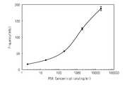
도 7은 본 발명의 실시예에 따른 바이오 랩온어칩의 항원에 양에 따른 공진 주파수의 천이 정도를 설명하기 위한 그래프이다.7 is a graph for explaining the degree of transition of the resonance frequency according to the amount of the antigen of the bio lab on chip according to an embodiment of the present invention.
도 7을 참조하면, 바이오 랩온어칩의 감지부 상에 구비된 항전립선 특이 항원 항체들과 반응하여 부착된 전립선 특이 항원들의 양에 따른, 공진 주파수를 측정한 그래프이다.Referring to FIG. 7, a resonance frequency is measured according to the amount of prostate-specific antigens attached to and reacted with anti-prostate-specific antigen antibodies provided on the sensing unit of the bio lab-on-a-chip.
감지부에 부착되는 전립선 특이 항원들의 양이 2ng/ml에서 20,000ng/ml까지의 범위 내에서 변화됨에 따라, 공진 주파수가 천이되는 것을 알 수 있다. 이러한 공진 주파수의 천이량은 감지부에 부착된 전립선 특이 항원들의 양에 대해 지수함수적으로 비례하는 경향을 보임을 알 수 있다. 즉, 감지부에 부착되는 항원들에 대한 정량적인 측정이 가능함을 알 수 있다.As the amount of prostate specific antigens attached to the detection unit is changed within the range of 2 ng / ml to 20,000 ng / ml, it can be seen that the resonance frequency is shifted. It can be seen that the amount of transition of the resonance frequency tends to be exponentially proportional to the amount of prostate specific antigens attached to the detector. That is, it can be seen that quantitative measurement of antigens attached to the detection unit is possible.
도 8a 내지 도 8j는 본 발명의 실시예에 따른 바이오 랩온어칩의 제조 방법을 설명하기 위해 도 1의 Ⅰ-Ⅰ' 선을 따라 절단한 단면도들이다.8A to 8J are cross-sectional views taken along the line II ′ of FIG. 1 to illustrate a method of manufacturing a bio lab-on-a-chip according to an embodiment of the present invention.
도 8a 및 도 8b를 참조하면, 기판(110)을 준비한다. 기판(110)은 실리콘, 유 리, 플라스틱, 금속 및 이들의 조합물 중에서 선택된 적어도 하나를 포함할 수 있다. 바람직하게는, 기판(110)은 실리콘 기판일 수 있다.8A and 8B, the
기판(110) 상에 실리콘 산화막(112)이 형성될 수 있다. 실리콘 산화막(112)은 압전 박막(114)을 따라 전달되어야 하는 표면 탄성파가 기판(110) 쪽으로 전달되어 손실되는 것을 최소화하기 위한 것일 수 있다.The
도 8c를 참조하면, 실리콘 산화막(112) 상에 압전 박막(114)이 형성될 수 있다. 압전 박막(114)은 0.1μm~10μm 범위의 두께를 갖게 형성될 수 있다. 바람직하게는, 압전 박막(114)은 0.5μm~10μm 범위의 두께를 갖게 형성될 수 있다.Referring to FIG. 8C, a piezoelectric
압전 박막(114)을 형성하는 단계는 기판(110) 상에 압전 물질을 증착하는 단계 및 증착된 압전 물질을 열 처리하는 단계를 포함할 수 있다. 압전 물질은 산화아연, 질화알루미늄, 니오브산리튬, 탄탈산리튬, 석영, 폴리머 및 이들의 조합물 중에서 선택된 적어도 하나를 포함할 수 있다. 압전 물질을 증착하는 단계는 반응성 스퍼터링(reactive sputtering) 방식, 화학 기상 증착(Chemical Vapor Deposition : CVD) 방식, 분자 빔 에피택시(molecular beam epitaxy) 방식, 원자층 증착(Atomic Layer Deposition : ALD) 방식 및 이들의 조합된 방식 중에서 선택된 적어도 하나의 방식을 포함할 수 있다. 바람직하게는, 압전 박막(114)은 산화아연을 반응성 스퍼터링 방식으로 약 5.5μm 정도의 두께로 증착한 후, 질소 분위기 하에서 400℃의 온도로 10분간 열 처리한 막일 수 있다. 압전 박막(114)에 대한 이러한 증착 방식은 증착된 압전 물질에 가해진 스트레스의 감소 및 압전 박막(114)의 결정성 향상을 위한 것일 수 있다.Forming the piezoelectric
도 8d 내지 도 8f를 참조하면, 압전 박막(114) 상에 포토레지스트(116)가 도포될 수 있다. 포토레지스트(116) 상에 마스크 패턴(118)이 제공될 수 있다. 마스크 패턴(118)을 마스크로 하는 사진식각 공정을 수행함으로써, 압전 박막(114) 상에 유체 제어부 영역(A, 감지용 인터디저테이티드 트랜스듀서 영역 포함) 및 감지부 영역(B)을 노출하는 포토레지스트 패턴(116a)이 형성될 수 있다.8D to 8F, a
도 8g 및 도 8h를 참조하면, 마스크 패턴(118)을 제거한 후, 포토레지스트 패턴(116a) 상 및 포토레지스트 패턴(116a)에 의해 노출된 압전 박막(114) 상에 도전성 금속막(120)이 형성될 수 있다. 도전성 금속막(120)은 금, 은, 알루미늄, 백금, 텅스텐, 니켈, 구리 및 이들의 조합물 중에서 선택된 적어도 하나를 포함할 수 있다.8G and 8H, after the
리프트-오프(lift-off) 방식으로 포토레지스트 패턴(116a) 및 포토레지스트 패턴(116a) 상의 도전성 금속막(120)이 제거될 수 있다. 이에 따라, 압전 박막(114) 상에 감지부(122s) 및 유체 제어부(122i, 감지용 인터디저테이티드 트랜스듀서 포함)가 형성될 수 있다. 유체 제어부(122i)는 인터디저테이티드 트랜스듀서 형태를 가질 수 있다.The
도 8i를 참조하면, 감지부(122s)와 유체 제어부(122i) 사이의 압전 박막(114) 상에 미세 유체 경로부(126)가 형성될 수 있다. 미세 유체 경로부(126)는 소수성 물질로 형성될 수 있다. 소수성 물질은 실란 화합물, 카본 나노 튜브 및 다이아몬드 카본 중에서 선택된 적어도 하나의 물질을 포함할 수 있다. 이에 따라, 액체 방울 형태의 미세 유체가 그 형태를 유지하면서 미세 유체 경로부(126)를 통 해 감지부(122s)로 이송될 수 있다.Referring to FIG. 8I, the
도시되지 않았지만, 감지부(122s) 상에 항체들(도 2a의 124 참조)이 형성되는 것을 더 포함할 수 있다. 항체들은 자가조립 단분자막 또는 단백질을 포함할 수 있다.Although not shown, the method may further include forming antibodies (see 124 of FIG. 2A) on the
도 8j를 참조하면, 감지부(122s) 및 미세 유체 경로부(126)를 둘러싸는 댐부(128)가 형성될 수 있다. 댐부(128)는 감광성 폴리머로 형성될 수 있다. 이에 따라, 액체 방울 형태의 미세 유체가 외부로 이탈하지 않고, 미세 유체 경로부(126)를 통해 감지부(122s)로 안정적으로 이송될 수 있다.Referring to FIG. 8J, a
도 9a 내지 도 9g는 본 발명의 다른 실시예에 따른 바이오 랩온어칩의 제조 방법을 설명하기 위해 도 1의 Ⅰ-Ⅰ' 선을 따라 절단한 단면도들이다.9A to 9G are cross-sectional views taken along the line II ′ of FIG. 1 to illustrate a method of manufacturing a bio lab-on-a-chip according to another embodiment of the present invention.
도 9a 및 도 9b를 참조하면, 기판(110)을 준비한다. 기판(110)은 실리콘, 유리, 플라스틱, 금속 및 이들의 조합물 중에서 선택된 적어도 하나를 포함할 수 있다. 바람직하게는, 기판(110)은 실리콘 기판일 수 있다.9A and 9B, the
기판(110) 상에 실리콘 산화막(112)이 형성될 수 있다. 실리콘 산화막(112)은 압전 박막(114)을 따라 전달되어야 하는 표면 탄성파가 기판(110) 쪽으로 전달되어 손실되는 것을 최소화하기 위한 것일 수 있다.The
도 9c 및 도 9d를 참조하면, 실리콘 산화막(112) 상에 유체 제어부(122i, 감지용 인터디저테이티드 트랜스듀서 포함)가 형성될 수 있다. 유체 제어부(122i)는 금, 은, 알루미늄, 백금, 텅스텐, 니켈, 구리 및 이들의 조합물 중에서 선택된 적어도 하나를 포함할 수 있다. 유체 제어부(122i)는 인터디저테이티드 트랜스듀서 형태를 가질 수 있다.9C and 9D, a
유체 제어부(122i)가 형성된 실리콘 산화막(112)을 덮도록 압전 박막(114)이 형성될 수 있다. 압전 박막(114)은 0.1μm~10μm 범위의 두께를 갖게 형성될 수 있다. 바람직하게는, 압전 박막(114)은 0.5μm~10μm 범위의 두께를 갖게 형성될 수 있다.The piezoelectric
압전 박막(114)을 형성하는 단계는 기판(110) 상에 압전 물질을 증착하는 단계 및 증착된 압전 물질을 열 처리하는 단계를 포함할 수 있다. 압전 물질은 산화아연, 질화알루미늄, 니오브산리튬, 탄탈산리튬, 석영, 폴리머 및 이들의 조합물 중에서 선택된 적어도 하나를 포함할 수 있다. 압전 물질을 증착하는 단계는 반응성 스퍼터링 방식, 화학 기상 증착 방식, 분자 빔 에피택시 방식, 원자층 증착 방식 및 이들의 조합된 방식 중에서 선택된 적어도 하나의 방식을 포함할 수 있다. 바람직하게는, 압전 박막(114)은 산화아연을 반응성 스퍼터링 방식으로 약 5.5μm 정도의 두께로 증착한 후, 질소 분위기 하에서 400℃의 온도로 10분간 열 처리한 막일 수 있다. 압전 박막(114)에 대한 이러한 증착 방식은 증착된 압전 물질에 가해진 스트레스의 감소 및 압전 박막(114)의 결정성 향상을 위한 것일 수 있다.Forming the piezoelectric
도 9e를 참조하면, 압전 박막(114) 상에 감지부(122s)가 형성될 수 있다. 감지부(122s)는 금, 은, 알루미늄, 백금, 텅스텐, 니켈, 구리 및 이들의 조합물 중에서 선택된 적어도 하나를 포함할 수 있다.Referring to FIG. 9E, a
도시되지 않았지만, 감지부(122s) 상에 항체들(도 2a의 124 참조)이 형성되는 것을 더 포함할 수 있다. 항체들은 자가조립 단분자막 또는 단백질을 포함할 수 있다.Although not shown, the method may further include forming antibodies (see 124 of FIG. 2A) on the
도 9f를 참조하면, 감지부(122s)와 유체 제어부(122i) 사이의 압전 박막(114) 상에 미세 유체 경로부(126)가 형성될 수 있다. 미세 유체 경로부(126)는 소수성 물질로 형성될 수 있다. 소수성 물질은 실란 화합물, 카본 나노 튜브 및 다이아몬드 카본 중에서 선택된 적어도 하나의 물질을 포함할 수 있다. 이에 따라, 액체 방울 형태의 미세 유체가 그 형태를 유지하면서 미세 유체 경로부(126)를 통해 감지부(122s)로 이송될 수 있다.Referring to FIG. 9F, a
도 9g를 참조하면, 감지부(122s) 및 미세 유체 경로부(126)를 둘러싸는 댐부(128)가 형성될 수 있다. 댐부(128)는 감광성 폴리머로 형성될 수 있다. 이에 따라, 액체 방울 형태의 미세 유체가 미세 유체 경로부(126)를 통해 감지부(122s)로 안정적으로 이송될 수 있다.Referring to FIG. 9G, a
상기와 같은 바이오 랩온어칩의 제조 방법들에 따라 제조된 바이오 랩온어칩은 압전 박막을 이용하여 나노리터 크기의 방울 용액 형태의 미세 유체를 이송, 정지, 반응 및 감지하기 때문에, 최소한의 시료를 사용하면서도 화학 분석의 모든 과정이 단일 칩 상에서 수행될 수 있다. 이에 따라, 분석 비용이 낮아질 수 있는 동시에 바이오 랩온어칩의 제조 비용도 낮아질 수 있다.Biolab-on-a-chip manufactured according to the above methods of manufacturing bio-lab-on-a-chip uses a piezoelectric thin film to transfer, stop, react and detect microfluids in the form of nanoliter droplets. In use, the entire process of chemical analysis can be performed on a single chip. Accordingly, the analysis cost may be lowered and the manufacturing cost of the bio lab-on-a-chip may be lowered.
상기한 본 발명의 실시예들에 따른 바이오 랩온어칩은 마이크로 크기의 방울 용액 형태의 미세 유체를 이송, 정지, 반응 및 감지하기 때문에, 생체 시료 및 시약의 낭비를 최소화할 수 있다. 이에 따라, 분석 비용이 낮아질 수 있다. 또한, 화학 분석의 모든 과정이 단일 칩에서 수행되기 때문에, 신속 및 정확한 분석이 가능 할 수 있다. 이에 더하여, 압전 박막이 고가의 벌크 기판을 대체하기 때문에, 제조 비용이 낮아질 수 있다. 추가로, 범용 반도체 제조 공정이 적용될 수 있기 때문에, 단백질 랩온어칩, 유전자 증폭 칩, 디엔에이 랩온어칩 또는 미세 생물/화학 반응기 등을 포함하는 다양한 바이오 랩온어칩 분야에 적용이 가능할 수 있다.Since the bio lab-on-a-chip according to the embodiments of the present invention transfers, stops, reacts, and senses microfluids in the form of microscopic droplet solutions, waste of biological samples and reagents can be minimized. Accordingly, the analysis cost can be lowered. In addition, since all the processes of chemical analysis are performed on a single chip, rapid and accurate analysis may be possible. In addition, since the piezoelectric thin film replaces the expensive bulk substrate, the manufacturing cost can be lowered. In addition, since a general-purpose semiconductor manufacturing process may be applied, it may be applicable to various bio lab-on-a-chip fields including protein lab-on-a-chip, gene amplification chip, DNA lab-on-a-chip or microbiological / chemical reactor.
도 1은 본 발명의 실시예에 따른 바이오 랩온어칩을 설명하기 위한 사시도;1 is a perspective view illustrating a bio lab-on-a-chip according to an embodiment of the present invention;
도 2a 내지 도 2d는 본 발명의 실시예에 따른 바이오 랩온어칩의 감지부에서 일어나는 반응을 구체적으로 설명하기 위한 개념 단면도들;2A to 2D are conceptual cross-sectional views for describing in detail a reaction occurring in a sensing unit of a bio lab-on-a-chip according to an embodiment of the present invention;
도 3a는 본 발명의 실시예에 따른 바이오 랩온어칩의 압전 박막을 설명하기 위한 주사 전자 현미경 사진;3A is a scanning electron micrograph for explaining a piezoelectric thin film of a bio lab-on-a-chip according to an embodiment of the present invention;
도 3b는 본 발명의 실시예에 따른 바이오 랩온어칩의 압전 박막의 결정 상태를 설명하기 위한 그래프;3B is a graph illustrating a crystal state of a piezoelectric thin film of a bio lab on chip according to an embodiment of the present invention;
도 4는 본 발명의 실시예에 따른 바이오 랩온어칩의 압전 박막의 공진 특성을 설명하기 위한 그래프;4 is a graph illustrating resonance characteristics of a piezoelectric thin film of a bio lab on chip according to an exemplary embodiment of the present invention;
도 5a 내지 도 5d는 본 발명의 실시예에 따른 바이오 랩온어칩의 감지부를 설명하기 위한 개념 단면도들;5A to 5D are conceptual cross-sectional views illustrating a sensing unit of a bio lab on chip according to an embodiment of the present invention;
도 6은 본 발명의 실시예에 따른 바이오 랩온어칩의 공진 주파수 및 진폭의 천이를 설명하기 위한 그래프;6 is a graph for explaining transition of resonant frequency and amplitude of a bio lab-on-a-chip according to an embodiment of the present invention;
도 7은 본 발명의 실시예에 따른 바이오 랩온어칩의 항원에 양에 따른 공진 주파수의 천이 정도를 설명하기 위한 그래프;7 is a graph for explaining the degree of transition of the resonance frequency according to the amount of the antigen of the bio lab on chip according to an embodiment of the present invention;
도 8a 내지 도 8j는 본 발명의 실시예에 따른 바이오 랩온어칩의 제조 방법을 설명하기 위해 도 1의 Ⅰ-Ⅰ' 선을 따라 절단한 단면도들;8A to 8J are cross-sectional views taken along line II ′ of FIG. 1 to illustrate a method of manufacturing a bio lab-on-a-chip according to an embodiment of the present invention;
도 9a 내지 도 9g는 본 발명의 다른 실시예에 따른 바이오 랩온어칩의 제조 방법을 설명하기 위해 도 1의 Ⅰ-Ⅰ' 선을 따라 절단한 단면도들.9A to 9G are cross-sectional views taken along the line II ′ of FIG. 1 to illustrate a method of manufacturing a bio lab-on-a-chip according to another embodiment of the present invention.
*도면의 주요 부분에 대한 부호의 설명** Description of the symbols for the main parts of the drawings *
110 : 기판112 : 실리콘 산화막110
114 : 압전 박막116 : 포토레지스트114: piezoelectric thin film 116: photoresist
116a : 포토레지스트 패턴118 : 마스크 패턴
120 : 도전성 금속막120: conductive metal film
122i, 122ia, 122ib, 122ic, 122id : 인터디저테이티드 트랜스듀서122i, 122ia, 122ib, 122ic, 122id: Interrupted Transducer
122s, 122sa, 122sb : 감지부124, 124a, 124b, 124c : 항체122s, 122sa, 122sb:
126 : 미세 유체 경로부128 : 댐부126: microfluidic path portion 128: dam portion
130a, 130b : 액체 방울 형태의 미세 유체132, 132a, 132b, 132c : 항원130a, 130b: microfluid in the form of a
Claims (42)
Translated fromKoreanPriority Applications (3)
| Application Number | Priority Date | Filing Date | Title |
|---|---|---|---|
| US12/740,348US20100304501A1 (en) | 2007-11-09 | 2007-11-09 | Bio lab-on-a-chip and method of fabricating and operating the same |
| KR1020070114116AKR100941065B1 (en) | 2007-11-09 | 2007-11-09 | Bio Lab-on-a-Chip, and Method of Manufacturing and Operating the Same |
| PCT/KR2007/005655WO2009061017A1 (en) | 2007-11-09 | 2007-11-09 | Bio lab-on-a-chip and method of fabricating and operating the same |
Applications Claiming Priority (1)
| Application Number | Priority Date | Filing Date | Title |
|---|---|---|---|
| KR1020070114116AKR100941065B1 (en) | 2007-11-09 | 2007-11-09 | Bio Lab-on-a-Chip, and Method of Manufacturing and Operating the Same |
Publications (2)
| Publication Number | Publication Date |
|---|---|
| KR20090047968A KR20090047968A (en) | 2009-05-13 |
| KR100941065B1true KR100941065B1 (en) | 2010-02-09 |
Family
ID=40625886
Family Applications (1)
| Application Number | Title | Priority Date | Filing Date |
|---|---|---|---|
| KR1020070114116AExpired - Fee RelatedKR100941065B1 (en) | 2007-11-09 | 2007-11-09 | Bio Lab-on-a-Chip, and Method of Manufacturing and Operating the Same |
Country Status (3)
| Country | Link |
|---|---|
| US (1) | US20100304501A1 (en) |
| KR (1) | KR100941065B1 (en) |
| WO (1) | WO2009061017A1 (en) |
Families Citing this family (24)
| Publication number | Priority date | Publication date | Assignee | Title |
|---|---|---|---|---|
| US7878063B1 (en)* | 2007-07-24 | 2011-02-01 | University Of South Florida | Simultaneous sample manipulation and sensing using surface acoustic waves |
| US20100140185A1 (en)* | 2008-12-05 | 2010-06-10 | John Hill | Wastewater treatment |
| US20130045474A1 (en)* | 2009-09-23 | 2013-02-21 | Drexel University | Devices and methods for detecting and monitoring hiv and other infections and diseases |
| US20110277193A1 (en) | 2010-04-20 | 2011-11-10 | Nanolnk, Inc. | Sensors and biosensors |
| KR101744339B1 (en) | 2010-05-03 | 2017-06-08 | 삼성전자주식회사 | Surface Acoustic Wave Sensor Device Including Target Biomolecule Isolation Component |
| DE102010036256B4 (en)* | 2010-09-03 | 2018-09-27 | Epcos Ag | Microacoustic device and manufacturing process |
| ITTO20110900A1 (en)* | 2011-10-10 | 2013-04-11 | Consiglio Nazionale Ricerche | PASSIVE AUTOMATIC CONTROL OF POSITIONING OF LIQUIDS IN MICROFLUID CHIPS |
| DE102011118742A1 (en)* | 2011-11-17 | 2013-05-23 | Forschungszentrum Jülich GmbH | Detector for magnetic particles in a liquid |
| CN102517205B (en)* | 2012-01-09 | 2013-04-17 | 青岛理工大学 | Heat transfer detection device based on DNA amplification |
| CN104870077A (en) | 2012-01-31 | 2015-08-26 | 宾夕法尼亚州立大学研究基金会 | Microfluidic manipulation and particle sorting using tunable surface standing acoustic waves |
| EP2879778B1 (en) | 2012-08-01 | 2020-09-02 | The Penn State Research Foundation | High efficiency separation and sorting of particles and cells |
| WO2014085627A1 (en) | 2012-11-27 | 2014-06-05 | The Penn State Research Foundation | Spatiotemporal control of chemical microenvironment using oscillating microstructures |
| CN102938397B (en)* | 2012-12-05 | 2015-09-09 | 苏州纳格光电科技有限公司 | Electronic device and preparation method thereof |
| KR101356933B1 (en)* | 2012-12-28 | 2014-01-29 | 고려대학교 산학협력단 | Apparatus and method for separating micro-nano scale particles using surface acoustic wave-based microfluidic chromatography |
| CN103223358B (en)* | 2013-03-29 | 2015-01-07 | 宁波大学 | Device and method of achieving digital microfluid cracking of acoustic surface waves |
| KR102122313B1 (en)* | 2013-08-12 | 2020-06-12 | 엘지전자 주식회사 | Biosensor capable of recognizing location of fluid and method of recognizing location of fluid using the same |
| KR101690603B1 (en)* | 2015-08-27 | 2017-01-13 | (주)라디안 | A defibrillator comprising a ladder bridge circuit |
| CN105181665B (en)* | 2015-09-18 | 2018-09-14 | 中国科学院苏州生物医学工程技术研究所 | Based on molecular dynamics test platform associated with acousto-optic |
| DE102018104669A1 (en)* | 2018-03-01 | 2019-09-05 | Dionex Softron Gmbh | Use of an acoustic wave in a chromatography system |
| CN112399887B (en)* | 2019-06-17 | 2023-02-07 | 京东方科技集团股份有限公司 | Detection chip and preparation method thereof |
| CN110653014B (en)* | 2019-10-28 | 2020-08-25 | 西安交通大学 | A device for generating a particle multilayer film structure based on surface acoustic waves |
| KR102436003B1 (en)* | 2020-03-19 | 2022-08-25 | 성균관대학교산학협력단 | Biosensor arrary for measuring conductivity and frequency change and manufacturing method thereof |
| CN111686828B (en)* | 2020-05-08 | 2023-05-02 | 杭州领挚科技有限公司 | Electrowetting microfluidic backboard and preparation method thereof |
| CN115616074A (en)* | 2022-09-15 | 2023-01-17 | 深圳大学 | On-chip laboratory based on multi-modal acoustic wave device and preparation method and application thereof |
Citations (4)
| Publication number | Priority date | Publication date | Assignee | Title |
|---|---|---|---|---|
| US6523392B2 (en) | 2000-01-25 | 2003-02-25 | Arizona Board Of Regents | Microcantilever sensor |
| KR20030025550A (en)* | 2001-09-21 | 2003-03-29 | 주식회사 나노위즈 | Radio frequency element using Micro Electro Mechanical System and Method of manufacturing the same |
| US20040072208A1 (en)* | 2002-05-23 | 2004-04-15 | Peter Warthoe | Surface acoustic wave sensors and method for detecting target analytes |
| KR20080052296A (en)* | 2006-12-05 | 2008-06-11 | 한국전자통신연구원 | Microfluidic transfer device and manufacturing method thereof |
Family Cites Families (9)
| Publication number | Priority date | Publication date | Assignee | Title |
|---|---|---|---|---|
| US4037176A (en)* | 1975-03-18 | 1977-07-19 | Matsushita Electric Industrial Co., Ltd. | Multi-layered substrate for a surface-acoustic-wave device |
| US5545531A (en)* | 1995-06-07 | 1996-08-13 | Affymax Technologies N.V. | Methods for making a device for concurrently processing multiple biological chip assays |
| US7147763B2 (en)* | 2002-04-01 | 2006-12-12 | Palo Alto Research Center Incorporated | Apparatus and method for using electrostatic force to cause fluid movement |
| US6981759B2 (en)* | 2002-04-30 | 2006-01-03 | Hewlett-Packard Development Company, Lp. | Substrate and method forming substrate for fluid ejection device |
| KR100523556B1 (en)* | 2002-12-26 | 2005-11-02 | 한국건설기술연구원 | A structure for supporting a electric light plate |
| KR100509254B1 (en)* | 2003-05-22 | 2005-08-23 | 한국전자통신연구원 | Micro-fluidic device to control flow time of micro-fluid |
| JP4533044B2 (en)* | 2003-08-27 | 2010-08-25 | キヤノン株式会社 | Sensor |
| US7943388B2 (en)* | 2003-11-14 | 2011-05-17 | 3M Innovative Properties Company | Acoustic sensors and methods |
| TWI330461B (en)* | 2006-01-12 | 2010-09-11 | Ind Tech Res Inst | Surface acoustic wave bio-chip |
- 2007
- 2007-11-09USUS12/740,348patent/US20100304501A1/ennot_activeAbandoned
- 2007-11-09WOPCT/KR2007/005655patent/WO2009061017A1/enactiveApplication Filing
- 2007-11-09KRKR1020070114116Apatent/KR100941065B1/ennot_activeExpired - Fee Related
Patent Citations (4)
| Publication number | Priority date | Publication date | Assignee | Title |
|---|---|---|---|---|
| US6523392B2 (en) | 2000-01-25 | 2003-02-25 | Arizona Board Of Regents | Microcantilever sensor |
| KR20030025550A (en)* | 2001-09-21 | 2003-03-29 | 주식회사 나노위즈 | Radio frequency element using Micro Electro Mechanical System and Method of manufacturing the same |
| US20040072208A1 (en)* | 2002-05-23 | 2004-04-15 | Peter Warthoe | Surface acoustic wave sensors and method for detecting target analytes |
| KR20080052296A (en)* | 2006-12-05 | 2008-06-11 | 한국전자통신연구원 | Microfluidic transfer device and manufacturing method thereof |
Also Published As
| Publication number | Publication date |
|---|---|
| WO2009061017A1 (en) | 2009-05-14 |
| US20100304501A1 (en) | 2010-12-02 |
| KR20090047968A (en) | 2009-05-13 |
Similar Documents
| Publication | Publication Date | Title |
|---|---|---|
| KR100941065B1 (en) | Bio Lab-on-a-Chip, and Method of Manufacturing and Operating the Same | |
| Li et al. | Gold nanoparticle-based low limit of detection Love wave biosensor for carcinoembryonic antigens | |
| US8580200B2 (en) | Method for label-free multiple analyte sensing, biosensing and diagnostic assay | |
| Ogi | Wireless-electrodeless quartz-crystal-microbalance biosensors for studying interactions among biomolecules: A review | |
| Nicu et al. | Biosensors and tools for surface functionalization from the macro-to the nanoscale: The way forward | |
| US20100297745A1 (en) | Flow-through method of functionalizing inner surfaces of a microfluidic device | |
| JP5487200B2 (en) | Surface plasmon resonance sensing device and method integrated with shear vertical surface acoustic wave | |
| WO2019192125A1 (en) | Biosensor based on surface acoustic wave mode and test method thereof | |
| HK1250681A1 (en) | Microfluidic valves and devices | |
| US20110298455A1 (en) | Integrated Microfluidic Sensor System with Magnetostrictive Resonators | |
| Tigli et al. | Fabrication and characterization of a surface-acoustic-wave biosensor in CMOS technology for cancer biomarker detection | |
| US8623284B2 (en) | Photonic crystal microarray layouts for enhanced sensitivity and specificity of label-free multiple analyte sensing, biosensing and diagnostic assay | |
| US11280784B2 (en) | Patterned plasmonic nanoparticle arrays for multiplexed, microfluidic biosensing assays | |
| Chen et al. | Low-noise fluorescent detection of cardiac troponin I in human serum based on surface acoustic wave separation | |
| CN112384797A (en) | Bulk acoustic wave resonator with increased dynamic range | |
| WO2003025547A1 (en) | Method and device for screening analytes using surface plasmon resonance | |
| US9452428B2 (en) | Method of making a microfluidic device | |
| CN112449743A (en) | Sensor with droplet retention structure | |
| KR101515155B1 (en) | Electrochemical immunoassay system utilizing gold doped silica nanoparticles, electrochemical immunoassay method and electrochemical immunoassay device using the same. | |
| US11344883B2 (en) | Microfluidic device with integrated waveguides for analyte identification and method of operation thereof | |
| WO2005106472A1 (en) | Biochip producing method, biochip, biochip analyzing device, biochip analyzing method | |
| US20240393331A1 (en) | Multiplexed electronic immunoassay using enzymaticall amplified metallization on nanostructured surfaces | |
| Dhiman et al. | On Microfluidics Devices for Clinical Biosensor | |
| Sakeeba | Performance optimization of conductometric biosensors | |
| Campifelli et al. | Development of microelectronic based biosensors |
Legal Events
| Date | Code | Title | Description |
|---|---|---|---|
| A201 | Request for examination | ||
| PA0109 | Patent application | St.27 status event code:A-0-1-A10-A12-nap-PA0109 | |
| PA0201 | Request for examination | St.27 status event code:A-1-2-D10-D11-exm-PA0201 | |
| D13-X000 | Search requested | St.27 status event code:A-1-2-D10-D13-srh-X000 | |
| D14-X000 | Search report completed | St.27 status event code:A-1-2-D10-D14-srh-X000 | |
| PG1501 | Laying open of application | St.27 status event code:A-1-1-Q10-Q12-nap-PG1501 | |
| PN2301 | Change of applicant | St.27 status event code:A-3-3-R10-R13-asn-PN2301 St.27 status event code:A-3-3-R10-R11-asn-PN2301 | |
| E902 | Notification of reason for refusal | ||
| PE0902 | Notice of grounds for rejection | St.27 status event code:A-1-2-D10-D21-exm-PE0902 | |
| P11-X000 | Amendment of application requested | St.27 status event code:A-2-2-P10-P11-nap-X000 | |
| P13-X000 | Application amended | St.27 status event code:A-2-2-P10-P13-nap-X000 | |
| E701 | Decision to grant or registration of patent right | ||
| PE0701 | Decision of registration | St.27 status event code:A-1-2-D10-D22-exm-PE0701 | |
| GRNT | Written decision to grant | ||
| PR0701 | Registration of establishment | St.27 status event code:A-2-4-F10-F11-exm-PR0701 | |
| PR1002 | Payment of registration fee | St.27 status event code:A-2-2-U10-U11-oth-PR1002 Fee payment year number:1 | |
| PG1601 | Publication of registration | St.27 status event code:A-4-4-Q10-Q13-nap-PG1601 | |
| L13-X000 | Limitation or reissue of ip right requested | St.27 status event code:A-2-3-L10-L13-lim-X000 | |
| U15-X000 | Partial renewal or maintenance fee paid modifying the ip right scope | St.27 status event code:A-4-4-U10-U15-oth-X000 | |
| FPAY | Annual fee payment | Payment date:20130201 Year of fee payment:4 | |
| PR1001 | Payment of annual fee | St.27 status event code:A-4-4-U10-U11-oth-PR1001 Fee payment year number:4 | |
| FPAY | Annual fee payment | Payment date:20140123 Year of fee payment:5 | |
| PR1001 | Payment of annual fee | St.27 status event code:A-4-4-U10-U11-oth-PR1001 Fee payment year number:5 | |
| FPAY | Annual fee payment | Payment date:20150126 Year of fee payment:6 | |
| PR1001 | Payment of annual fee | St.27 status event code:A-4-4-U10-U11-oth-PR1001 Fee payment year number:6 | |
| PN2301 | Change of applicant | St.27 status event code:A-5-5-R10-R13-asn-PN2301 St.27 status event code:A-5-5-R10-R11-asn-PN2301 | |
| FPAY | Annual fee payment | Payment date:20160127 Year of fee payment:7 | |
| PR1001 | Payment of annual fee | St.27 status event code:A-4-4-U10-U11-oth-PR1001 Fee payment year number:7 | |
| FPAY | Annual fee payment | Payment date:20170124 Year of fee payment:8 | |
| PR1001 | Payment of annual fee | St.27 status event code:A-4-4-U10-U11-oth-PR1001 Fee payment year number:8 | |
| PR1001 | Payment of annual fee | St.27 status event code:A-4-4-U10-U11-oth-PR1001 Fee payment year number:9 | |
| LAPS | Lapse due to unpaid annual fee | ||
| PC1903 | Unpaid annual fee | St.27 status event code:A-4-4-U10-U13-oth-PC1903 Not in force date:20190202 Payment event data comment text:Termination Category : DEFAULT_OF_REGISTRATION_FEE | |
| PC1903 | Unpaid annual fee | St.27 status event code:N-4-6-H10-H13-oth-PC1903 Ip right cessation event data comment text:Termination Category : DEFAULT_OF_REGISTRATION_FEE Not in force date:20190202 |