KR100937613B1 - Backplanes for Electro-Optical Displays - Google Patents
Backplanes for Electro-Optical DisplaysDownload PDFInfo
- Publication number
- KR100937613B1 KR100937613B1KR1020087011300AKR20087011300AKR100937613B1KR 100937613 B1KR100937613 B1KR 100937613B1KR 1020087011300 AKR1020087011300 AKR 1020087011300AKR 20087011300 AKR20087011300 AKR 20087011300AKR 100937613 B1KR100937613 B1KR 100937613B1
- Authority
- KR
- South Korea
- Prior art keywords
- electro
- backplane
- electrode
- display
- layer
- Prior art date
- Legal status (The legal status is an assumption and is not a legal conclusion. Google has not performed a legal analysis and makes no representation as to the accuracy of the status listed.)
- Expired - Fee Related
Links
Images


Classifications
- G—PHYSICS
- G02—OPTICS
- G02F—OPTICAL DEVICES OR ARRANGEMENTS FOR THE CONTROL OF LIGHT BY MODIFICATION OF THE OPTICAL PROPERTIES OF THE MEDIA OF THE ELEMENTS INVOLVED THEREIN; NON-LINEAR OPTICS; FREQUENCY-CHANGING OF LIGHT; OPTICAL LOGIC ELEMENTS; OPTICAL ANALOGUE/DIGITAL CONVERTERS
- G02F1/00—Devices or arrangements for the control of the intensity, colour, phase, polarisation or direction of light arriving from an independent light source, e.g. switching, gating or modulating; Non-linear optics
- G02F1/01—Devices or arrangements for the control of the intensity, colour, phase, polarisation or direction of light arriving from an independent light source, e.g. switching, gating or modulating; Non-linear optics for the control of the intensity, phase, polarisation or colour
- G02F1/13—Devices or arrangements for the control of the intensity, colour, phase, polarisation or direction of light arriving from an independent light source, e.g. switching, gating or modulating; Non-linear optics for the control of the intensity, phase, polarisation or colour based on liquid crystals, e.g. single liquid crystal display cells
- G02F1/133—Constructional arrangements; Operation of liquid crystal cells; Circuit arrangements
- G02F1/136—Liquid crystal cells structurally associated with a semi-conducting layer or substrate, e.g. cells forming part of an integrated circuit
- G02F1/1362—Active matrix addressed cells
- G02F1/1365—Active matrix addressed cells in which the switching element is a two-electrode device
- H—ELECTRICITY
- H01—ELECTRIC ELEMENTS
- H01H—ELECTRIC SWITCHES; RELAYS; SELECTORS; EMERGENCY PROTECTIVE DEVICES
- H01H59/00—Electrostatic relays; Electro-adhesion relays
- H01H59/0009—Electrostatic relays; Electro-adhesion relays making use of micromechanics
- G—PHYSICS
- G02—OPTICS
- G02F—OPTICAL DEVICES OR ARRANGEMENTS FOR THE CONTROL OF LIGHT BY MODIFICATION OF THE OPTICAL PROPERTIES OF THE MEDIA OF THE ELEMENTS INVOLVED THEREIN; NON-LINEAR OPTICS; FREQUENCY-CHANGING OF LIGHT; OPTICAL LOGIC ELEMENTS; OPTICAL ANALOGUE/DIGITAL CONVERTERS
- G02F1/00—Devices or arrangements for the control of the intensity, colour, phase, polarisation or direction of light arriving from an independent light source, e.g. switching, gating or modulating; Non-linear optics
- G02F1/01—Devices or arrangements for the control of the intensity, colour, phase, polarisation or direction of light arriving from an independent light source, e.g. switching, gating or modulating; Non-linear optics for the control of the intensity, phase, polarisation or colour
- G02F1/13—Devices or arrangements for the control of the intensity, colour, phase, polarisation or direction of light arriving from an independent light source, e.g. switching, gating or modulating; Non-linear optics for the control of the intensity, phase, polarisation or colour based on liquid crystals, e.g. single liquid crystal display cells
- G02F1/133—Constructional arrangements; Operation of liquid crystal cells; Circuit arrangements
- G02F1/136—Liquid crystal cells structurally associated with a semi-conducting layer or substrate, e.g. cells forming part of an integrated circuit
- G02F1/1362—Active matrix addressed cells
- G—PHYSICS
- G02—OPTICS
- G02F—OPTICAL DEVICES OR ARRANGEMENTS FOR THE CONTROL OF LIGHT BY MODIFICATION OF THE OPTICAL PROPERTIES OF THE MEDIA OF THE ELEMENTS INVOLVED THEREIN; NON-LINEAR OPTICS; FREQUENCY-CHANGING OF LIGHT; OPTICAL LOGIC ELEMENTS; OPTICAL ANALOGUE/DIGITAL CONVERTERS
- G02F1/00—Devices or arrangements for the control of the intensity, colour, phase, polarisation or direction of light arriving from an independent light source, e.g. switching, gating or modulating; Non-linear optics
- G02F1/01—Devices or arrangements for the control of the intensity, colour, phase, polarisation or direction of light arriving from an independent light source, e.g. switching, gating or modulating; Non-linear optics for the control of the intensity, phase, polarisation or colour
- G02F1/165—Devices or arrangements for the control of the intensity, colour, phase, polarisation or direction of light arriving from an independent light source, e.g. switching, gating or modulating; Non-linear optics for the control of the intensity, phase, polarisation or colour based on translational movement of particles in a fluid under the influence of an applied field
- G02F1/166—Devices or arrangements for the control of the intensity, colour, phase, polarisation or direction of light arriving from an independent light source, e.g. switching, gating or modulating; Non-linear optics for the control of the intensity, phase, polarisation or colour based on translational movement of particles in a fluid under the influence of an applied field characterised by the electro-optical or magneto-optical effect
- G02F1/167—Devices or arrangements for the control of the intensity, colour, phase, polarisation or direction of light arriving from an independent light source, e.g. switching, gating or modulating; Non-linear optics for the control of the intensity, phase, polarisation or colour based on translational movement of particles in a fluid under the influence of an applied field characterised by the electro-optical or magneto-optical effect by electrophoresis
- H—ELECTRICITY
- H01—ELECTRIC ELEMENTS
- H01H—ELECTRIC SWITCHES; RELAYS; SELECTORS; EMERGENCY PROTECTIVE DEVICES
- H01H59/00—Electrostatic relays; Electro-adhesion relays
- G—PHYSICS
- G02—OPTICS
- G02F—OPTICAL DEVICES OR ARRANGEMENTS FOR THE CONTROL OF LIGHT BY MODIFICATION OF THE OPTICAL PROPERTIES OF THE MEDIA OF THE ELEMENTS INVOLVED THEREIN; NON-LINEAR OPTICS; FREQUENCY-CHANGING OF LIGHT; OPTICAL LOGIC ELEMENTS; OPTICAL ANALOGUE/DIGITAL CONVERTERS
- G02F1/00—Devices or arrangements for the control of the intensity, colour, phase, polarisation or direction of light arriving from an independent light source, e.g. switching, gating or modulating; Non-linear optics
- G02F1/01—Devices or arrangements for the control of the intensity, colour, phase, polarisation or direction of light arriving from an independent light source, e.g. switching, gating or modulating; Non-linear optics for the control of the intensity, phase, polarisation or colour
- G02F1/13—Devices or arrangements for the control of the intensity, colour, phase, polarisation or direction of light arriving from an independent light source, e.g. switching, gating or modulating; Non-linear optics for the control of the intensity, phase, polarisation or colour based on liquid crystals, e.g. single liquid crystal display cells
- G02F1/133—Constructional arrangements; Operation of liquid crystal cells; Circuit arrangements
- G02F1/136—Liquid crystal cells structurally associated with a semi-conducting layer or substrate, e.g. cells forming part of an integrated circuit
- G02F1/1362—Active matrix addressed cells
- G02F1/136213—Storage capacitors associated with the pixel electrode
Landscapes
- Physics & Mathematics (AREA)
- Nonlinear Science (AREA)
- Optics & Photonics (AREA)
- Chemical & Material Sciences (AREA)
- General Physics & Mathematics (AREA)
- Mathematical Physics (AREA)
- Crystallography & Structural Chemistry (AREA)
- Microelectronics & Electronic Packaging (AREA)
- Engineering & Computer Science (AREA)
- Health & Medical Sciences (AREA)
- Life Sciences & Earth Sciences (AREA)
- Chemical Kinetics & Catalysis (AREA)
- Electrochemistry (AREA)
- Molecular Biology (AREA)
- Electrochromic Elements, Electrophoresis, Or Variable Reflection Or Absorption Elements (AREA)
- Devices For Indicating Variable Information By Combining Individual Elements (AREA)
- Micromachines (AREA)
- Control Of Indicators Other Than Cathode Ray Tubes (AREA)
Abstract
Translated fromKoreanDescription
Translated fromKorean본 발명은 전기-광학 디스플레이용 백플레인, 및 이러한 백플레인을 형성하는 프로세스에 관한 것이다. 본 발명의 백플레인은 특히 전기적으로 충전된 파티클 중 하나 이상의 형태가 디스플레이의 외관 (appearance) 을 바꾸도록 액체에서 부유하고 전기장의 영향 하에서 액체를 통해 이동하는 입자-기반의 전기영동 (electrophoretic) 디스플레이에 사용되도록 의도되지만 이 용도에만 배타적으로 사용되도록 의도되는 것은 아니다.The present invention relates to a backplane for an electro-optical display and to a process for forming such a backplane. The backplane of the present invention is particularly used for particle-based electrophoretic displays in which one or more forms of electrically charged particles are suspended in the liquid so as to change the appearance of the display and move through the liquid under the influence of an electric field. It is intended to, but is not intended to be used exclusively for this purpose.
재료 또는 디스플레이에 적용되는 용어 "전기-광학" 은, 본 명세서에서 이미징 기술에서의 종래 의미로, 하나 이상의 광학 특성이 상이한 제 1 및 제 2 디스플레이 상태를 가지는 재료를 지시하는데 사용되며, 재료는 재료에 전기장을 인가함으로써, 제 1 디스플레이 상태에서 제 2 디스플레이 상태로 변경된다. 상기한 광학 특성은 일반적으로는 인간의 눈으로 감지할 수 있는 색채이지만, 광학적 투과 (optical transmission), 반사, 발광 (luminescence) 또는, 기계 판독을 의도한 디스플레이의 경우에, 가시 범위 외의 전자기 파장의 반사율의 변화의 감지의 의사 색채 (pseudeo-color) 와 같은 다른 광학 특성이 될 수도 있다.The term “electro-optical” as applied to a material or display is used herein to refer to a material having first and second display states in which one or more optical properties differ in a conventional sense in imaging technology, where the material is a material By applying an electric field to the switch, the display state is changed from the first display state to the second display state. The above optical properties are generally colors that can be perceived by the human eye, but in the case of displays intended for optical transmission, reflection, luminescence, or machine reading, the wavelengths of electromagnetic wavelengths outside the visible range Other optical properties may be such as pseudo-color of detection of changes in reflectance.
이미징 기술에서 종래 의미로 용어 "회색 상태 (gray state)" 는, 이미징 기술에서 종래 의미로, 픽셀의 2 개의 극단적인 광학 상태들 사이의 중간적 상태를 지시하는데 사용되고, 이 2 가지 극단적인 상태들 사이의 흑-백 변화 (black-white transition) 를 반드시 의미하지는 않는다. 예를 들어, 아래에 언급된 여러 특허들과 공개된 출원들은, 극단적인 상태들이 백색과 짙은 청색 (deep blue) 인 전기영동 디스플레이를 기술하여서, 중간적 "회색 상태" 는 실제로 엷은 청색 (pale blue) 을 의미할 것이다. 실제로, 이미 언급된 바와 같이, 2 개의 극단적인 상태 사이의 변화는 색상 변화가 전혀 아닐 수도 있다.The term "gray state" in the conventional sense in the imaging technique is used to indicate an intermediate state between two extreme optical states of the pixel, in the conventional sense in the imaging technique, the two extreme states It does not necessarily mean a black-white transition between them. For example, several of the patents and published applications mentioned below describe electrophoretic displays in which the extreme states are white and deep blue, so that the intermediate "grey state" is actually pale blue. Will mean). Indeed, as already mentioned, the change between two extreme states may not be a color change at all.
용어 "쌍안정 (bistable)" 및 "쌍안정성 (bistablity)" 은, 본 명세서에서 당업계에서의 종래 의미로, 하나 이상의 광학 특성이 상이한 제 1 및 제 2 디스플레이 상태를 가지는 디스플레이 요소를 포함하는 디스플레이를 지시하는데 사용되며, 주어진 디스플레이 구성요소가 제 1 또는 제 2 디스플레이 상태 중의 하나를 취하도록 유한한 지속 시간의 어드레싱 펄스를 이용하여 구동되어진 후, 어드레싱 펄스가 종료된 후에 그 상태가 디스플레이 구성요소의 상태를 변경하기 위해 요구되는 어드레싱 펄스의 최소 지속 시간의 적어도 몇 배, 예컨대 적어도 4 배 동안 유지될 것이다. 몇몇의 입자 기반의 그레이 스케일이 가능한 전기영동 디스플레이들은 극단적인 흑과 백 상태뿐만 아니라 중간적인 회색 상태에서도 안정적 일 수 있으며, 전기-광학 디스플레이의 몇몇의 다른 유형들에도 동일하게 적용될 수 있다는 것이 공개된 미국 특허 출원 제 2002/0180687 호에 나타난다. 이러한 유형의 디스플레이는 쌍안정 보다는 "다중-안정 (multi-stable)" 이라 불리는 것이 적합하나, 편의상 용어 "쌍안정" 은 본 명세서에서 쌍안정 디스플레이 및 다중-안정의 디스플레이 모두를 포괄하도록 사용될 수 있다.The terms "bistable" and "bistablity", as used herein in the conventional sense, include a display element having display elements having first and second display states that differ in at least one optical property. Used to indicate that a given display component is driven using a finite duration addressing pulse to take one of the first or second display states, and then after the addressing pulse has ended the state of the display component. It will be held for at least several times, for example at least four times, the minimum duration of the addressing pulses required to change the state. It has been published that some particle-based grayscale electrophoretic displays can be stable not only in extreme black and white states, but also in intermediate gray states, and equally applicable to some other types of electro-optic displays. US Patent Application No. 2002/0180687. This type of display is suitably referred to as "multi-stable" rather than bistable, but for convenience the term "bistable" may be used herein to encompass both bistable displays and multi-stable displays. .
몇몇 유형의 전기-광학 디스플레이들이 공지되어 있다. 일 유형의 전기-광학 디스플레이는 회전 이색 부재 유형으로서, 예를 들어 미국 특허 제 5,808,783 호; 제 5,777,782 호; 제 5,760,761 호; 제 6,054,071 호; 제 6,055,091 호; 제 6,097,531 호; 제 6,128,124 호; 제 6,137,467 호; 및 제 6,147,791 호 (이 유형의 디스플레이는 종종 "회전 이색성 구 (rotation bichromal ball)" 디스플레이로 인용되기도 하지만, 상기 언급된 몇몇의 특허에서는 회전 부재가 구형 (spherical) 이 아니기 때문에 용어 "회전 이색성 부재"가 보다 정확한 것으로 선호된다). 이러한 디스플레이는 상이한 광학 특징을 가진 2 개 이상의 섹션을 가지는 많은 수의 작은 몸체들 (일반적으로 구형 또는 원기둥형) 과 내부 쌍극자 (dipole) 를 사용한다. 이러한 몸체들은 매트릭스 내의 액체로 채워진 액포 (vacuoles) 에 매달리며, 액포는 몸체가 자유롭게 회전하도록 액체로 채워진다. 디스플레이의 외관은, 그곳에 전기장을 인가하여 다양한 위치로 몸체를 회전시키고, 관찰면을 통하여 보여지는 몸체들의 섹션들이 변경되도록 하여 변화한다. 이 유형의 전기-광학 매체는 전형적으로 쌍안정성이다.Several types of electro-optic displays are known. One type of electro-optic display is a rotating dichroic member type, for example US Pat. No. 5,808,783; 5,777,782; 5,777,782; 5,760,761; 5,760,761; 6,054,071; 6,054,071; 6,055,091; 6,055,091; 6,097,531; 6,097,531; No. 6,128,124; No. 6,137,467; And 6,147,791 (this type of display is often referred to as a "rotation bichromal ball" display, but in some of the patents mentioned above the term "rotary dichroism" is not known because the rotating member is not spherical). Absence "is preferred to be more accurate). Such displays use a large number of small bodies (generally spherical or cylindrical) and internal dipoles with two or more sections with different optical characteristics. These bodies are suspended in vacuoles filled with liquid in the matrix, which are filled with liquid so that the body rotates freely. The appearance of the display changes by applying an electric field there to rotate the body to various positions and cause sections of the bodies to be viewed through the viewing plane to change. Electro-optical media of this type are typically bistable.
다른 유형의 전기-광학 디스플레이는 전기-착색 (electrochromic) 매체, 예를 들어, 적어도 부분적으로 반도체 금속 산화물로 형성된 전극 및 전극에 부착된 가역적 색채 변환 가능한 복수의 색조 분자를 포함하는 나노크로믹 (nanochromic) 막의 형태의 전기-착색 매체를 사용하며, 예컨대, O'Regan, B. 외, Nature 1991, 353,737; 및 Wood, D., Information Display, 18(3), 24 (2002년 3월) 에 개시되어 있다. 또한 Bach, U. 외, Adv. Mater., 2002, 14(11), 845 에도 개시되어 있다. 이 유형의 나노크로믹 막은 또한 예를 들어, 미국 특허 제 6,301,038호, 국제 출원 공보 제 WO 01/27690 호, 및 미국 특허 출원 제 2003/0214695 호에 기술되어 있다. 이 유형의 매체도 또한 전형적으로 쌍안정성이다.Another type of electro-optic display is a nanochromic comprising an electrochromic medium, for example an electrode formed at least partially of a semiconductor metal oxide and a plurality of reversible color convertible color molecules attached to the electrode. ) Using an electro-coloring medium in the form of a membrane, for example O'Regan, B. et al., Nature 1991, 353,737; And Wood, D., Information Display, 18 (3), 24 (March 2002). See also Bach, U. et al., Adv. Mater., 2002, 14 (11), 845. Nanochromic films of this type are also described, for example, in US Pat. No. 6,301,038, International Application Publication WO 01/27690, and US Patent Application 2003/0214695. Media of this type are also typically bistable.
수년 동안 열성적인 연구 및 개발의 주제가 되어온 다른 유형의 전기-광학 디스플레이는, 복수의 충전된 입자들이 전기장의 영향 아래에서 부유하는 유동체 (fluid) 를 통해 이동하는, 입자-기반 전기영동 디스플레이이다. 전기영동 디스플레이는 액정 디스플레이 (LCD) 와 비교하여, 우수한 명도 및 대비, 넓은 시야각, 상태 쌍안정성, 및 낮은 전력 소모의 특질을 가질 수 있다. 그럼에도 불구하고, 이러한 디스플레이의 장기간의 이미지 품질에 대한 문제가 이 디스플레이들이 널리 사용되는 것을 막아왔다. 예를 들어, 전기영동 디스플레이를 구성하는 입자는 정착 (settle) 하려고 하는 경향이 있어서, 이 디스플레이에 대하여 적합하지 않은 서비스-수명을 초래한다.Another type of electro-optic display, which has been the subject of dedicated research and development for many years, is a particle-based electrophoretic display, in which a plurality of charged particles move through a floating fluid under the influence of an electric field. Electrophoretic displays can have the characteristics of superior brightness and contrast, wide viewing angle, state bistable, and low power consumption compared to liquid crystal displays (LCDs). Nevertheless, the problem of long-term image quality of such displays has prevented them from being widely used. For example, particles that make up electrophoretic displays tend to settle, resulting in unsuitable service-life for these displays.
Massachusetts Institute of Technology (MIT) 및 E Ink Corporation 에게 양도되거나 그 명의로 출원된 다수의 특허 및 출원은 최근에 공개되어 캡슐화 전기영동 매체 (encapsulated electrophoretic media) 를 기술하고 있다. 이러한 갭슐화 매체는 각각 액체 부유 매체에 부유하는 전기영동적으로 이동가능한 입자를 포함하는 내부 상 (internal phase), 및 내부 상을 둘러싸는 캡슐 벽을 포함하는 다수의 작은 캡슐을 포함한다. 일반적으로, 캡슐은 2 개의 전극 사이에 위치하 는 밀착된 층을 형성하도록 폴리머 바인더 (polymeric binder) 에서 고정된다. 이 유형의 캡슐화 매체는 예를 들어, 미국 특허 제 5,930,026 호; 제 5,961,804 호; 제 6,017,584 호; 제 6,067,185 호; 제 6,118,426 호; 제 6,120,588 호; 제 6,120,839 호; 제 6,124,851 호; 제 6,130,773 호; 제 6,130,774 호; 제 6,172,798 호; 제 6,177,921 호; 제 6,232,950 호; 제 6,249,721 호; 제 6,252,564 호; 제 6,262,706 호; 제 6,262,833 호; 제 6,300,932 호; 제 6,312,304 호; 제 6,312,971 호; 제 6,323,989 호; 제 6,327,072 호; 제 6,376,828 호; 제 6,377,387 호; 제 6,392,785 호; 제 6,392,786 호; 제 6,413,790 호; 제 6,422,687 호; 제 6,445,374 호; 제 6,445,489 호; 제 6,459,418 호; 제 6,473,072 호; 제 6,480,182 호; 제 6,498,114 호; 제 6,504,524 호; 제 6,506,438 호; 제 6,512,354 호; 제 6,515,649 호; 제 6,518,949 호; 제 6,521,489 호; 제 6,531,997 호; 제 6,535,197 호; 제 6,538,801 호; 제 6,545,291 호; 제 6,580,545 호; 제 6,639,578 호; 제 6,652,075 호; 및 제 6,657,772 호; 및 미국 특허 출원 공보 제 2002/0019081 호; 제 2002/0021270 호; 제 2002/0053900 호; 제 2002/0060321 호; 제 2002/0063661 호; 제 2002/0063677 호; 제 2002/0090980 호; 제 2002/0106847 호; 제 2002/0113770 호; 제 2002/0130832 호; 제 2002/0131147 호; 제 2002/0145792 호; 제 2002/0171910 호; 제 2002/0180687 호; 제 2002/0180688 호; 제 2002/0185378 호; 제 2003/0011560 호; 제 2003/0011868 호; 제 2003/0020844 호; 제 2003/0025855 호; 제 2003/0034949 호; 제 2003/0038755 호; 제 2003/0053189 호; 제 2003/0076573 호; 제 2003/0096113 호; 제 2003/0102858 호; 제 2003/0132908 호; 제 2003/0137521 호; 제 2003/0137717 호; 제 2003/01151702 호; 및 제 2003/0214697 호 및 국제 출원 공보 제 WO 99/67678 호; 제 WO 00/05704 호; 제 WO 00/38000 호; 제 WO 00/38001 호; 제 WO 00/36560 호; 제 WO 00/67110 호; 제 WO 00/67327 호; 제 WO 01/07961 호; 및 제 WO 01/08241 호에서 설명된다.Numerous patents and applications assigned to or filed under the names of Massachusetts Institute of Technology (MIT) and E Ink Corporation have recently been published to describe encapsulated electrophoretic media. Such encapsulation media comprises an internal phase comprising electrophoretic movable particles, each suspended in a liquid suspended medium, and a plurality of small capsules comprising a capsule wall surrounding the interior phase. In general, the capsule is fixed in a polymeric binder to form a tight layer positioned between two electrodes. Encapsulation media of this type are described, for example, in US Pat. No. 5,930,026; No. 5,961,804; No. 6,017,584; No. 6,067,185; No. 6,118,426; No. 6,120,588; No. 6,120,839; No. 6,124,851; 6,130,773; 6,130,773; No. 6,130,774; 6,172,798; 6,172,798; No. 6,177,921; No. 6,232,950; No. 6,249,721; 6,252,564; 6,252,564; 6,262,706; 6,262,706; No. 6,262,833; No. 6,300,932; No. 6,312,304; No. 6,312,971; No. 6,323,989; No. 6,327,072; No. 6,376,828; No. 6,377,387; No. 6,392,785; No. 6,392,786; 6,413,790; 6,413,790; No. 6,422,687; No. 6,445,374; No. 6,445,489; No. 6,459,418; No. 6,473,072; No. 6,480,182; No. 6,498,114; 6,504,524; 6,504,524; No. 6,506,438; No. 6,512,354; No. 6,515,649; No. 6,518,949; No. 6,521,489; 6,531,997; 6,531,997; No. 6,535,197; 6,538,801; 6,538,801; No. 6,545,291; No. 6,580,545; No. 6,639,578; No. 6,652,075; And 6,657,772; And US Patent Application Publication No. 2002/0019081; 2002/0021270; 2002/0053900; 2002/0060321; 2002/0063661; 2002/0063677; 2002/0090980; 2002/0106847; 2002/0113770; 2002/0130832; 2002/0131147; 2002/0145792; 2002/0171910; 2002/0180687; 2002/0180688; US 2002/0185378; 2003/0011560; 2003/0011868; 2003/0020844; 2003/0025855; US2003 / 0034949; 2003/0038755; 2003/0053189; 2003/0076573; 2003/0096113; 2003/0102858; 2003/0132908; 2003/0137521; 2003/0137717; 2003/01151702; And 2003/0214697 and International Application Publication No. WO 99/67678; WO 00/05704; WO 00/38000; WO 00/38001; WO 00/36560; WO 00/67110; WO 00/67327; WO 01/07961; And WO 01/08241.
상술한 특허들 및 출원들 중 많은 수는, 캡슐화 전기영동 매체의 분리된 (discrete) 마이크로캡슐을 둘러싸는 벽들이 연속적인 상 (continuous phase) 으로 변화되어, 전기영동 매체가 복수의 분리된 전기영동 유동체의 액적 (droplet) 및 폴리머 재료의 연속적인 상을 포함하는 소위 폴러머-분산 (polymer-dispersed) 전기영동 디스플레이를 제조한다는 것과, 이러한 폴리머 분산 전기영동 디스플레이내에서의 전기영동 유동체의 분리된 액적은, 어떠한 분리된 캡슐 막 (membrane) 이 각각의 액적에 결합되어 있지 않더라도 캡슐 또는 마이크로캡슐로서 간주될 수 있다는 것을 인식하며, 예를 들어 위에 언급된 제 2002/0131147 호에서 설명된다. 따라서, 본 출원의 목적으로, 이러한 폴리머-분산 전기영동 매체는 캡슐화 전기영동 매체의 하위 형태 (sub-species) 로 간주될 수 있다.Many of the patents and applications described above allow the walls surrounding discrete microcapsules of encapsulated electrophoretic medium to be changed in a continuous phase such that the electrophoretic medium is subjected to a plurality of discrete electrophoresis. Producing so-called polymer-dispersed electrophoretic displays comprising droplets of fluids and continuous phases of polymer material, and separate liquids of electrophoretic fluids in such polymer dispersed electrophoretic displays. Little recognize that any discrete capsule membrane can be considered as a capsule or microcapsule even if it is not bound to each droplet, and is described, for example, in 2002/0131147 mentioned above. Thus, for the purposes of the present application, such polymer-dispersed electrophoretic media may be considered as sub-species of encapsulated electrophoretic media.
캡슐화 전기영동 디스플레이는 일반적으로, 전통적인 전기영동 장치의 크러스터링 (clustening) 과 세틀링 (settling) 실패 모드를 겪지 않고, 여러가지의 유연하고 고정된 기판 상에 디스플레이를 프린트 또는 코팅하는 능력과 같은 추가적인 이점을 제공한다.( 단어 "프린팅 (printing)" 의 사용은 제한 없이, 패치 다이 코팅, 슬롯 또는 압출 코팅, 슬라이드 또는 직렬 코팅, 커튼 코팅과 같은 선-측정 (pre-metered coating) 코팅; 나이프 오버 롤 코팅, 전 및 후 롤 코팅과 같은 롤 코팅; 그라비아 코팅; 딥 코팅; 스프레이 코팅; 매니스커스 코팅; 스핀 코팅; 브러쉬 코팅; 에어 나이프 코팅; 실크 스크린 프린팅 프로세스; 정전기 프린팅 프로세스; 열 프린팅 프로세스; 잉크 젯 프린팅 프로세스; 및 다른 유사 기술을 포함하는 프린팅 및 코팅의 모든 형태를 포함하도록 지시된다.) 따라서, 완성된 디스플레이는 가요성이 있을 수 있다. 또한, 디스플레이 매체가 (다양한 방법을 이용하여) 프린팅될 수 있기 때문에, 디스플레이 자체가 저렴하게 제조될 수 있다.Encapsulated electrophoretic displays generally have additional benefits, such as the ability to print or coat the display on a variety of flexible, fixed substrates without undergoing the clustering and settling failure modes of traditional electrophoretic devices. (The use of the word "printing" includes, without limitation, pre-metered coating coatings such as patch die coating, slot or extrusion coating, slide or tandem coating, curtain coating; knife over roll Roll coatings such as coating, before and after roll coating; gravure coating; dip coating; spray coating; meniscus coating; spin coating; brush coating; air knife coating; silk screen printing process; electrostatic printing process; thermal printing process; ink To include all forms of printing and coatings, including jet printing processes; and other similar technologies. Is.) Thus, the completed display may be flexible. In addition, since the display medium can be printed (using various methods), the display itself can be manufactured at low cost.
관련된 유형의 전기영동 디스플레이는 소위 "마이크로셀 전기영동 디스플레이 (microcell electrophoretic display)" 이다. 마이크로셀 전기영동 디스플레이이에서, 충전된 입자들 및 부유하는 유동체는 캡슐 내에 캡슐화되지 않지만 대신에 수송 매체, 일반적으로 폴리머 막에서 형성된 복수의 공동 (cavity) 에서 유지된다. 예를 들어, Sipix Imaging, Inc 에 양도된 2 개의 국제 출원 공보 제 WO 02/01281 호, 및 공개된 미국 출원 제 2002/0075556 호에서 개시된다.A related type of electrophoretic display is the so-called "microcell electrophoretic display". In microcell electrophoretic displays, the charged particles and floating fluid are not encapsulated in capsules but instead remain in a plurality of cavities formed in a transport medium, generally a polymer membrane. For example, two international application publications WO 02/01281 assigned to Sipix Imaging, Inc, and published US application 2002/0075556 are disclosed.
액정 디스플레이를 포함하는 다른 유형의 전기-광학 디스플레이도 또한 본 발명의 백플레인을 이용할 수 있다.Other types of electro-optical displays, including liquid crystal displays, may also utilize the backplane of the present invention.
명백하게, 전기-광학 디스플레이가 작동하기 위해서, 전기-광학 매체를 그 다양한 광학상태들로 스위칭하기 위해서 전기 광학 매체를 가로지르는 제어 가능한 전기장의 공급을 위해서 전극들을 배열하는 것이 필요하며, 따라서 매체의 양면 상에 전극들을 배열하는 것이 필요하다. 디스플레이의 가장 단순한 형태에서, 디스플레이의 각각의 픽셀은 다양한 전압 레벨들에 스위칭 가능한 접속을 자체적으로 제공받는 개별 전극과 연결된다. 다만, 예를 들어 VGA (640×480) 디스플레이 와 같은 고 해상도 디스플레이에서는, 이 구조는 많은 수의 전기적 리드선이 요구되기 때문에 비실용적으로 된다. 따라서, 전기-광학 층 (electro-optic layer) 의 한 면 상에, 디스플레이의 모든 픽셀을 가로질러 연장되는 단일 공통, 투명 전극을 가지는 액티브 매트릭스 디스플레이 구조를 사용하는 것은 이러한 디스플레이에서 일반적이다. 전형적으로, 이 공통 전극은 전기-광학 층과 관찰자 사이에 위치하고 이를 통해 관찰자가 디스플레이를 관찰하는 관찰 면을 형성한다. 전기-광학 층의 반대 면 상에, 각 픽셀 전극이 단일 행과 단일 열의 교차로써 유일하게 정의되도록 행들과 열들로 배열되는 픽셀 전극들의 매트릭스가 위치한다. 따라서, 전기-광학 층의 각각의 픽셀에 의해 생기는 전기장은 공통 전면 전극에 인가하는 전압에 호응하여, 연관된 픽셀 전극에 인가하는 전압을 변화시킴으로써 제어된다. 다이오드도 사용될 수 있지만, 각각의 픽셀 전극은 적어도 비-선형 소자, 일반적으로는 박막 트랜지스터와 결합된다. 각각의 열 내의 트랜지스터들의 게이트는 단일 연장 열 전극을 통해 열 드라이버에 접속된다. 각각의 열 내의 트랜지스터들의 소스 전극들은 단일 연장 열 전극을 통해 열 드라이버에 접속된다. 각각의 트랜지스터의 드레인 전극들은 픽셀 전극에 직접적으로 접속된다. 행들에 대한 게이트들의 할당과 열들에 대한 소스 전극들의 할당은 임의적이며 소스 및 드레인 전극들의 할당이 가능한 것처럼 반대가 될 수 있다. 비-선형적 소자들의 배열 및 장치들의 연관된 행 및 열 전극은 디스플레이의 백플레인을 형성하며, 이 백플레인은 동일한 물리적 유닛에서 행 및 열 드라이버 회로를 포함할 것이다. 많은 전기-광학 디스플레이에서, 액티브 매트릭스 구조는 상대적으로 복 잡한 백플레인이 종래의 반도체 제조 기술을 사용하는 디스플레이의 나머지 부분과는 독립적으로 제조될 수 있도록 한다. 예를 들어, 디스플레이의 나머지 부분 또는 전면 부분은 인듐 주석 산화물 (indium tin oxide; ITO) 또는 유기 폴리머 컨덕터로부터 형성되는 실질적으로 투명한 도전층이 먼저 증착된 폴리머막 상에 전기-광학 매체의 층을 증착시킴으로써 값싸게 제조될 수 있다. 따라서, 디스플레이의 전면 부분은 일반적으로 백플레인에 적층된다.Obviously, in order for an electro-optical display to work, it is necessary to arrange the electrodes for the supply of a controllable electric field across the electro-optical medium in order to switch the electro-optical medium into its various optical states, so that both sides of the medium It is necessary to arrange the electrodes on the top. In the simplest form of the display, each pixel of the display is connected with a separate electrode which is itself provided with a switchable connection at various voltage levels. However, in high resolution displays such as VGA (640 × 480) displays, this structure is impractical because a large number of electrical leads are required. Thus, it is common in such displays to use an active matrix display structure having a single common, transparent electrode extending on one side of an electro-optic layer across all pixels of the display. Typically, this common electrode is located between the electro-optical layer and the observer, thereby forming an observation plane through which the observer observes the display. On the opposite side of the electro-optical layer is located a matrix of pixel electrodes arranged in rows and columns such that each pixel electrode is uniquely defined as the intersection of a single row and a single column. Thus, the electric field generated by each pixel of the electro-optical layer is controlled by varying the voltage applied to the associated pixel electrode in response to the voltage applied to the common front electrode. Diodes may also be used, but each pixel electrode is at least coupled with a non-linear element, typically a thin film transistor. The gates of the transistors in each column are connected to the column driver through a single extension column electrode. The source electrodes of the transistors in each column are connected to the column driver through a single extension column electrode. The drain electrodes of each transistor are connected directly to the pixel electrode. The assignment of gates to rows and the assignment of source electrodes to columns are arbitrary and can be reversed, as the assignment of source and drain electrodes is possible. The array of non-linear elements and the associated row and column electrodes of the devices form the backplane of the display, which will include row and column driver circuits in the same physical unit. In many electro-optic displays, the active matrix structure allows a relatively complex backplane to be fabricated independently of the rest of the display using conventional semiconductor fabrication techniques. For example, the remainder or front portion of the display may deposit a layer of electro-optical medium on a polymer film first deposited with a substantially transparent conductive layer formed from indium tin oxide (ITO) or an organic polymer conductor. It can be manufactured inexpensively. Thus, the front portion of the display is typically stacked on the backplane.
상술한 바와 같이, 디스플레이 백플레인들은 반도체 제조 기술을 사용하여 제조된다. 다만, 이러한 기술들의 현 상태는 백플레인 제조에 최적화되지 않았다. 반도체 제조 기술은, 컴퓨터 내의 중앙 처리 장치 ("CPU") 와 다른 논리 장치로서 사용되는 초고밀도 집적회로 (enormous complex integrated circuits; "chips") 를 제조하기 위한 필요에 의하여 추진되어 왔다. 이러한 CPU 는 각각의 유닛에 수백만개의 트랜지스터를 공급하는 것을 요구하고, CPU 에서 소진되는 열을 최소화해야하는 요구와, 각각의 처리된 반도체 웨이퍼 상에 가능한 많은 CPU 를 형성해야하는 경제적인 필요 (하나의 웨이퍼를 처리하는 비용은 본질적으로 한 웨이퍼 내에 형성된 CPU의 개수와는 무관하기 때문) 모두가 매우 높은 트랜지스터의 팩킹 (packing) 밀도를 이끌며, 최신의 CPU 는, 개별적인 피쳐 (feature) 가 약 0.13 ㎛ 만큼 작을 수 있고, 개별적인 트랜지스터가 1 ㎛ 제곱의 차수를 가지며, 인접한 트랜지스터들 간의 간격이 동일한 크기의 차수를 가지는 기술에 의해서 제 조된다. 이러한 작은 트랜지스터들과 높은 팩킹 밀도는 0.1 ㎜ 의 치수의 간격으로 위치하는 전형적인 픽셀, 및 트랜지스터 또는 비-선형 소자를 가지는 디스플레이 백플레인에는 필요하지 않다. 또한, 백플레인은 전형적으로 100 제곱 ㎜ 의 치수이고 (더 클 수 있으며), 그러므로 칩 (chip) 보다는 크기가 훨씬 크다. 결과적으로, 백플레인 제조의 단위 면적 당 비용을 감소시켜야 하는 큰 필요가 있다.As mentioned above, display backplanes are fabricated using semiconductor fabrication techniques. However, the current state of these technologies is not optimized for backplane manufacturing. Semiconductor fabrication techniques have been driven by the need to fabricate highly complex integrated circuits ("chips") that are used as central processing units ("CPUs") and other logic devices in computers. These CPUs require the supply of millions of transistors to each unit, the need to minimize the heat dissipated in the CPU, and the economic need to form as many CPUs as possible on each processed semiconductor wafer. Because the cost of processing is essentially independent of the number of CPUs formed in a wafer) all lead to a very high packing density of transistors, while modern CPUs can have individual features as small as about 0.13 μm. And individual transistors have orders of 1 μm square, and the spacing between adjacent transistors is made by the same order of magnitude. Such small transistors and high packing density are not required for a typical pixel located at intervals of dimensions of 0.1 mm, and for a display backplane with transistors or non-linear elements. In addition, the backplane is typically a dimension of 100 square millimeters (can be larger) and is therefore much larger in size than a chip. As a result, there is a great need to reduce the cost per unit area of backplane manufacturing.
본 발명은 백플레인에서의 다양한 개선점들과 그 제조 프로세스를 제공한다.The present invention provides various improvements in the backplane and its manufacturing process.
따라서, 일 양태에서 본 발명은 픽셀 전극, 픽셀 전극에 전압을 공급하도록 배열되는 전압 공급 라인, 및 전압 공급 라인과 상기 픽셀 전극 사이에 위치한 마이크로기계식 스위치를 포함하고, 마이크로기계식 스위치는, 전압 공급 라인이 상기 픽셀 전극에 전기적으로 접속되지 않은 개방 상태 (open state) 및 상기 전압 공급 라인이 상기 픽셀 전극에 전기적으로 접속된 폐쇄 상태 (closed state) 를 가지는, 전기-광학 디스플레이용 백플레인을 제공한다.Thus, in one aspect the invention includes a pixel electrode, a voltage supply line arranged to supply a voltage to the pixel electrode, and a micromechanical switch located between the voltage supply line and the pixel electrode, the micromechanical switch comprising: a voltage supply line An open state not electrically connected to the pixel electrode and a closed state in which the voltage supply line is electrically connected to the pixel electrode are provided.
본 발명의 본 양태는 이하 편리하게 본 발명의 "MEMS" 백플레인이라 한다. 이러한 MEMS 백플레인의 한 형태에서, 마이크로기계식 스위치는 제 1 전극과 접속 및 비 접속 상태가 될 수 있는 캔틸레버 빔, 및 캔틸레버 빔을 이동시키도록 배열되는 제 2 전극을 포함한다. 이러한 MEMS 백플레인은, 제 1 전극과 인접하여 위치하여서 캐패시터 전극과 제 1 전극이 캐패시터를 형성하는 캐패시터 전극을 더 포함할 수 있다. MEMS 백플레인은 마이크로기계식 스위치를 커버하는 캡슐화층 을 제공받을 수 있다.This aspect of the invention is hereinafter referred to conveniently as the "MEMS" backplane of the invention. In one form of such a MEMS backplane, the micromechanical switch includes a cantilever beam that can be connected and unconnected with the first electrode, and a second electrode arranged to move the cantilever beam. The MEMS backplane may further include a capacitor electrode positioned adjacent to the first electrode such that the capacitor electrode and the first electrode form a capacitor. The MEMS backplane can be provided with an encapsulation layer covering the micromechanical switch.
본 발명은 MEMS 백플레인을 포함하는 전기-광학 디스플레이 ("MEMS 디스플레이") 로 확장된다. 그러므로, 다른 양태에서, 본 발명은 적어도 하나의 광학적 특성이 상이한 제 1 디스플레이 상태 및 제 2 디스플레이 상태를 가지는 전기-광학 매체의 층으로서, 전기-광학 매체는 매체에 전기장을 인가함으로써 제 1 디스플레이 상태에서 제 2 디스플레이 상태로 변경될 수 있는, 전기-광학 매체의 층; 및 전기-광학 매체의 층에 인접하여 위치하고, 전압을 인가할 때 전기장을 상기 전기-광학 매체에 인가하도록 배열된 픽셀 전극을 포함하며, 전압을 픽셀 전극에 공급하도록 배열되는 전압 공급 라인을 더 포함하는, 백플레인을 포함하는 전기-광학 디스플레이로서, 마이크로 기계식 스위치가 전압 공급 라인과 픽셀 전극 사이에 위치하고, 전압 공급 라인이 픽셀 전극에 전기적으로 접속되지 않은 개방 상태 (open state) 및 전압 공급 라인이 상기 픽셀 전극에 전기적으로 접속된 폐쇄 상태 (closed state) 를 가지는, 전기-광학 디스플레이를 제공한다.The present invention extends to electro-optical displays ("MEMS displays") that include MEMS backplanes. Therefore, in another aspect, the invention is a layer of an electro-optical medium having a first display state and a second display state that differ in at least one optical property, the electro-optical medium being a first display state by applying an electric field to the medium. A layer of electro-optical medium, which can be changed from to a second display state; And a pixel electrode positioned adjacent the layer of electro-optical medium and arranged to apply an electric field to the electro-optical medium when applying a voltage, the voltage supply line being arranged to supply a voltage to the pixel electrode. An electro-optic display comprising a backplane, wherein a micromechanical switch is positioned between the voltage supply line and the pixel electrode, the open state and voltage supply line of which the voltage supply line is not electrically connected to the pixel electrode. An electro-optic display having a closed state electrically connected to a pixel electrode.
이러한 MEMS 디스플레이는, 백플레인으로부터 전기-광학 매체의 층의 반대 면 상에 위치하는 광 투과성 전극을 더 포함할 수 있다. MEMS 디스플레이 내의 전기-광학 매체는 상술한 유형들 중 하나일 수 있다. 그러므로, 예를 들어, 전기-광학 매체는 교대하는 이색성 부재 또는 전기-착색 매체일 수 있다. 다른 방법으로, 전기-광학 매체는 전기영동 입자가 전기영동 입자가 실제 캡슐 벽 (true capsule wall) 으로 캡슐화될 수 있는 유형, 폴리머-확산 유형 또는 마이크로셀 유형의 캡슐화 전기영동 매체일 수 있다.Such a MEMS display may further comprise a light transmissive electrode located on the opposite side of the layer of electro-optical medium from the backplane. The electro-optical medium in the MEMS display can be one of the types described above. Thus, for example, the electro-optical medium can be an alternating dichroic member or an electro-colored medium. Alternatively, the electro-optical medium may be an encapsulated electrophoretic medium of the type, polymer-diffusion type or microcell type, in which the electrophoretic particles can be encapsulated into the true capsule wall.
본 발명은 또한, 기판을 제공하는 단계;The invention also provides a method of providing a substrate comprising: providing a substrate;
기판 상에 제 1 전극, 제 2 전극, 및 제 3 전극을 형성하는 단계;Forming a first electrode, a second electrode, and a third electrode on the substrate;
그 다음으로, 제 1 전극 및 제 2 전극을 커버하지만 적어도 제 3 전극의 일부는 노출되도록 남기는 희생층을 상기 기판 상에 형성하는 단계;Thereafter, forming a sacrificial layer on the substrate covering the first electrode and the second electrode but leaving at least a portion of the third electrode exposed;
그 다음으로, 제 3 전극의 노출된 부분과 접속하는 제 1 섹션, 및 적어도 제 2 전극과 상기 제 1 전극 각각의 일부에 걸쳐 연장하기 위해 희생층을 걸쳐 연장되는 제 2 섹션을 가지는 캔틸레버 빔을 형성하도록 상기 기판 상에 도전성 재료를 증착하는 단계; 및Next, a cantilever beam having a first section connecting with the exposed portion of the third electrode and a second section extending over the sacrificial layer to extend over at least the second electrode and a portion of each of the first electrodes. Depositing a conductive material on the substrate to form; And
그 다음으로, 상기 제 2 전극에 인가하는 전압의 영향 하에서 상기 캔틸레버 빔의 제 2 전극 섹션이 상기 제 1 전극의 접속 여부와 자유롭게 접속되거나 접속되지 않도록 할 수 있도록, 상기 희생층을 제거하는 단계를 포함하는, 전기-광학 디스플레이용 백플레인을 형성하는 프로세스를 제공한다.Thereafter, removing the sacrificial layer so that the second electrode section of the cantilever beam can be freely connected or not connected with or without the first electrode under the influence of the voltage applied to the second electrode. Providing a process for forming a backplane for an electro-optic display.
본 프로세스에서, 기판 상에 도전성 재료를 증착하는 단계는 캐패시터 전극과 제 1 전극이 함께 캐패시터를 형성하도록 상기 캔틸레버 빔 부재에 떨어져서 위치하지만 상기 제 1 전극의 부분 위에 위치하는 상기 캐패시터 전극을 증착하는 단계를 더 포함할 수 있다. 본 프로세스는 또한 희생층을 제거하는 단계 후에, 적어도 캔틸레버 빔 부재를 커버하도록 상기 기판 상에 캡슐화층을 증착하는 단계를 포함할 수 있다.In the present process, the step of depositing a conductive material on the substrate comprises depositing the capacitor electrode located away from the cantilever beam member but above a portion of the first electrode such that the capacitor electrode and the first electrode together form a capacitor. It may further include. The process may also include depositing an encapsulation layer on the substrate to at least cover the cantilever beam member after removing the sacrificial layer.
다른 양태에서, 본 발명은, 기판 상에 적어도 하나의 전자 부품을 형성할 수 있는 부품 재료층을 형성하는 단계;In another aspect, the present invention provides a method for forming an electronic component comprising: forming a component material layer capable of forming at least one electronic component on a substrate;
부품 재료층 상에 엠보싱 가능 재료층을 형성하는 단계;Forming an embossable material layer on the part material layer;
적어도 하나의 제 1 부분 및 적어도 하나의 제 1 부분의 두께보다 두꺼운 두께를 가지는 적어도 하나의 제 2 부분를 형성하도록 엠보싱 가능 재료층을 화상방식 (imagewise) 엠보싱하는 단계;Imagewise embossing the layer of embossable material to form at least one second portion having a thickness greater than at least one first portion and at least one first portion;
적어도 하나의 제 2 부분에 존재하는 엠보싱 가능 재료를 남기는 반면에 상기 적어도 하나의 제 1 부분을 제거하도록, 엠보싱 가능 재료의 적어도 하나의 제 1 부분 하에 위치한 부품 재료를 노출하도록 하는, 상기 엠보싱 가능 재료을 에칭하는 단계; 및Exposing the part material located under at least one first portion of the embossable material to remove the at least one first portion while leaving the embossable material present in the at least one second portion. Etching; And
그 다음, 부품 재료의 노출된 부분들을 에칭하여, 부품 재료층을 패터닝하고 그 내부에 적어도 하나의 전자 부품를 형성하는 단계를 포함하는, 기판 상에 전자 회로의 적어도 하나의 전자 부품을 형성하는 프로세스를 제공한다.And then etching the exposed portions of the part material to pattern the part material layer and to form at least one electronic part therein, thereby forming at least one electronic part of the electronic circuit on the substrate. to provide.
본 발명의 이 양태는 이하 편리하게 본 발명의 엠보싱 프로세스라 한다. 엠보싱 프로세스는, 부품 재료층을 패터닝한 후, 기판에서 엠보싱 가능 재료를 제거하는 단계를 포함 할 수 있다. 엠보싱 가능 재료의 화상방식 엠보싱은 롤러에 의해 달성될 수 있다. 엠보싱 가능 재료는 감광제를 포함할 수 있다. 감광제는 감광제로부터 용매를 제거하기 위해 그 화상방식 엠보싱 전에 가열 ("소프트 베이킹") 될 수 있다. 다른 방법으로 또는 추가적으로, 감광제는 적어도 하나의 제 1 부분을 제거하는 에칭 후, 부품 재료의 에칭 전에 가열 ("하드 베이킹") 될 수 있다.This aspect of the invention is hereinafter referred to conveniently as the embossing process of the invention. The embossing process may include removing the embossable material from the substrate after patterning the layer of component material. Imaging embossing of the embossable material may be accomplished by rollers. The embossable material may comprise a photosensitizer. The photosensitizer may be heated (“soft bake”) before its imaging embossing to remove the solvent from the photosensitizer. Alternatively or additionally, the photosensitizer may be heated (“hard bake”) after etching to remove at least one first portion and before etching of the part material.
엠보싱 가능 재료는 적어도 하나의 기저 가용성 단위체로부터 추출된 반복되 는 유닛을 가지는 공중합체를 포함할 수 있다. 이 적어도 하나의 기저 가용성 단위체는 산을 직면해서 블록이 해제되는 블록킹 그룹을 포함할 수 있다. 이 목적을 위한 바람직한 공중합체는 4-하이드록시스티린과 메타아크릴레이트로부터 추출된 반복되는 유닛을 가지는 것을 포함한다.The embossable material may comprise a copolymer having repeating units extracted from at least one base soluble unit. The at least one base soluble monomer may comprise a blocking group in which the block is released in the face of an acid. Preferred copolymers for this purpose include those having repeating units extracted from 4-hydroxystyrene and methacrylate.
마지막으로, 본 발명은, 기판;Finally, the present invention, substrate;
기판 상에 위치하는 트랜지스터;A transistor located on the substrate;
트랜지스터를 커버하는 보호층;A protective layer covering the transistor;
트랜지스터로부터 상기 보호층의 반대 면에 위치한 픽셀 전극; 및A pixel electrode located on an opposite side of the protective layer from a transistor; And
보호층을 통과하고 상기 픽셀 전극에 트랜지스터를 전기적으로 접속하는 도전성 비아를 포함하고,A conductive via passing through the protective layer and electrically connecting the transistor to the pixel electrode,
보호층은 에폭시, 폴리우레탄, 실리콘, 폴리아크릴레이트 및 폴리이미드 폴리머들로 이루어진 그룹으로부터 선택된 폴리머를 포함하는, 전기-광학 디스플레이용 백플레인을 제공한다.The protective layer provides a backplane for an electro-optical display, comprising a polymer selected from the group consisting of epoxy, polyurethane, silicone, polyacrylate, and polyimide polymers.
본 발명의 본 양태는 이하 편의상 본 발명의 "매몰된 트랜지스터" 백플레인이라 한다. 이러한 매몰된 트랜지스터 백플레인에서, 보호층은 열 경화성 폴리머 또는 방사 경화성 폴리머로 형성될 수 있다. 이러한 매몰된 트랜지스터 백플레인의 바람직한 형태에서, 기판은 절연층으로 커버되는 금속막을 포함하고, 트랜지스터는 절연층 상에 형성된다. 기판은, 예를 들어, 폴리이미드 절연층으로 커버되는 스텐인리스 스틸 포일을 포함할 수 있다.This aspect of the invention is hereinafter referred to as the " embedded transistor " backplane of the invention for convenience. In such buried transistor backplanes, the protective layer may be formed of a thermosetting polymer or a radiation curable polymer. In a preferred form of such a buried transistor backplane, the substrate comprises a metal film covered with an insulating layer, and the transistor is formed on the insulating layer. The substrate may, for example, comprise a stainless steel foil covered with a polyimide insulating layer.
본 발명은 본 별명의 매몰된 트랜지스터 백플레인을 포함하는 전기-광학 디 스플레이로 확장된다. 따라서 본 발명은, 적어도 하나의 광학적 특성이 상이한 제 1 디스플레이 상태 및 제 2 디스플레이 상태를 가지는 전기-광학 매체의 층으로서,The present invention extends to an electro-optical display that includes the buried transistor backplane of the present nickname. The present invention therefore provides a layer of an electro-optical medium having a first display state and a second display state that differ in at least one optical property,
전기-광학 매체는 매체에 전기장을 인가함으로써 제 1 디스플레이 상태에서 제 2 디스플레이 상태로 변경될 수 있는, 전기-광학 매체의 층; 및The electro-optical medium includes a layer of electro-optical medium, which can be changed from a first display state to a second display state by applying an electric field to the medium; And
전기-광학 매체의 층에 인접하여 위치하고 픽셀 전극에 전압을 인가할 때, 전기장을 전기-광학 매체에 인가하도록 배열되는 본 발명의 매몰된 트랜지스터 백플레인을 포함하는, 전기-광학 디스플레이를 제공한다.An electro-optic display is provided, comprising an implanted transistor backplane of the present invention positioned adjacent to a layer of electro-optic medium and arranged to apply an electric field to the electro-optic medium when voltage is applied to the pixel electrode.
이 전기-광학 디스플레이는 상술한 전기-광학 매체의 유형 중 하나를 사용할 것이다.This electro-optic display will use one of the types of electro-optical media described above.
본 발명은 트랜지스터 및 전기-광학 디스플레이의 백플레인에 사용되는 다른 비-선형 소자의 보호에 대해 낮은 비용의 프로세스를 제공한다.The present invention provides a low cost process for the protection of transistors and other non-linear devices used in the backplane of electro-optic displays.
이미 지적한 것처럼, 본 발명은 각각 전기-광학 디스플레이용 백플레인에서 개선점을 제공하는, 수개의 상이한 양태들을 가지며, 본 발명의 어떤 양태들은 다른 응용에서 또한 유용할 수 있다. 이하, 본 발명의 주요 양태를 개별적으로 설명할 것이지만, 본 발명의 하나 이상의 양태가 단일 백플레인 또는 다른 전자 부품의 제조에 사용될 수 있다는 것을 알아야한다. 예를 들어, 본 발명의 MEMS 백플레인은 본 발명의 엠보싱 방법을 사용하여 제조될 수 있다.As already pointed out, the present invention has several different aspects, each providing an improvement in the backplane for electro-optical displays, and certain aspects of the present invention may also be useful in other applications. While the main aspects of the present invention will be described individually below, it should be appreciated that one or more aspects of the present invention may be used in the manufacture of a single backplane or other electronic component. For example, the MEMS backplane of the present invention can be made using the embossing method of the present invention.
파트part A: A:MEMSMEMS백플레인Backplane
이미 상술한 것처럼, 종래 기술의 액티브 매트릭스 디스플레이는 각각 픽셀에서 비-선형 (트랜지스터 또는 다이오드) 스위칭 구성요소를 요구한다. 최근 비-선형 트랜지스터 구성요소는 비정형 실리콘, 폴리실리콘 및 유기 반도체로 제조될 수 있다. 다이오드 스위칭 구성요소는 금속 절연체 금속 (MIM; metal insulator metal), 금속 반도체 절연체 (MSI; metal semiconductor insulator), 쇼트키 (Schottky), 및 NIN 다이오드를 포함한다. 이러한 스위칭 구성요소들은, 전기-광학 디스플레이들을 구동할 수 있는 반면에 특정한 단점들을 가진다.As already mentioned above, prior art active matrix displays require a non-linear (transistor or diode) switching component in each pixel. Recent non-linear transistor components can be made of amorphous silicon, polysilicon and organic semiconductors. Diode switching components include metal insulator metal (MIM), metal semiconductor insulator (MSI), Schottky, and NIN diodes. Such switching components can drive electro-optical displays, while having certain drawbacks.
비정형 및 다결정 실리콘에 기초한 트랜지스터들은 안정된 소자를 생산하기 위해 비교적 높은 온도 (>200℃) 의 증착 단계를 요구한다. 실제로 이러한 높은 온도 프로세싱에 대한 요구는, 열 팽창의 계수의 차이가 특정 크기 이상의 부정합 (mis-registration) 을 유발할 수 있기 때문에, 제조에서 사용될 수 있는 가요성 기판의 최대 크기를 제한한다. (위에서 지적한 것처럼, 특정 유형의 전기-광학 디스플레이의 매력적인 특성 중 하나는 디스플레이가 가요성 기판 상에 형성될 수 있고, 따라서 종래 액정 디스플레이에서 가능하지 않았던 가요성이고 견고한 유형의 디스플레이를 제공한다는 것이다.) 금속 포일과 같은 치수적으로 안정된 가요성 기판은 연마 단계, 평탄화 단계 및 보호 단계와 같은 추가적인 프로세싱 단계를 요구한다. 유기 트랜지스터는 낮은 온도에서 제조할 수 있지만 짧은 동작 수명을 가지고 산소와 습기에 민감한 경향이 있다. 스위칭 구성요소중 어느 하나의 유형의 온/오프 (on/off) 비율은 바람직한 것보다 작고 반도체층의 실리콘 이동도 (비정형 실리콘에 대해서는 1.0 ㎠/Vs 미만이고 다결정 실리콘에 대해서는 300 ㎠/Vs 미만) 에 의해 제한된다. 트랜지스터 스위치들은 상대적으로 큰 게이트 대 픽셀 누설 캐패시턴스를 가지며 픽셀에서 직류 전압 불균형을 유도하는 전압 커플링을 유발하므로, 그러므로 디스플레이된 이미지에 바람직하지 않은 아티팩트 (artifact) 를 유발한다.Transistors based on amorphous and polycrystalline silicon require deposition steps of relatively high temperatures (> 200 ° C.) to produce stable devices. Indeed, the need for such high temperature processing limits the maximum size of flexible substrates that can be used in fabrication, since differences in coefficients of thermal expansion can cause mis-registration above a certain size. (As pointed out above, one of the attractive characteristics of certain types of electro-optical displays is that the display can be formed on a flexible substrate, thus providing a flexible and robust type of display that was not possible in conventional liquid crystal displays. Dimensionally stable flexible substrates, such as metal foils, require additional processing steps such as polishing, planarization, and protection. Organic transistors can be manufactured at low temperatures but have a short operating life and tend to be sensitive to oxygen and moisture. The on / off ratio of either type of switching component is less than desirable and the silicon mobility of the semiconductor layer (less than 1.0 cm 2 / Vs for amorphous silicon and less than 300 cm 2 / Vs for polycrystalline silicon). Limited by Transistor switches have a relatively large gate-to-pixel leakage capacitance and cause voltage coupling that induces direct voltage unbalance in the pixel, thus causing undesirable artifacts in the displayed image.
다이오드는 매우 큰 선택 라인 대 기생 캐패시턴스를 가지므로 엄격한 설계 규칙을 요구한다. 또한, 상기 제 WO 01/07961 호에서 설명된 이유 때문에, 픽셀을 가로지르는 구동 전압을 유지하기 위해, 백플레인에 각각의 픽셀에 대한 캐패시터를 제공하는 것이 유리하고, 다이오드 기반의 백플레인에서는 이러한 캐패시터를 제공하는 것이 곤란하다.Diodes have very large select line-to-parasitic capacitances, requiring strict design rules. In addition, for the reasons described in WO 01/07961, it is advantageous to provide a capacitor for each pixel in the backplane, in order to maintain a drive voltage across the pixel, in diode-based backplanes. It is difficult to do
본 발명의 MEMS 백플레인은 종래 기술의 백플레인의 이러한 문제를 줄이거나 제거한다. 전기-광학 디스플레이에 대한 이러한 MEMS 백플레인의 바람직한 형태는 복수의 마이크로전자기계식시스템 (MEMS; MicroElectroMechanicalSystem) 스위치를 가지고 전기영동 디스플레이와 같은 평평한 패널 디스플레이를 어드레싱하는데 유용하다.The MEMS backplane of the present invention reduces or eliminates this problem of prior art backplanes. This preferred form of MEMS backplane for electro-optic displays is useful for addressing flat panel displays such as electrophoretic displays with a plurality of MicroElectroMechanical System (MEMS) switches.
이하, 이러한 MEMS 백플레인을 제조하는 본 발명의 바람직한 프로세스는 실례를 통해, 제조 프로세스 내의 다양한 단계에서 단일 MEMS 스위치의 개략적인 측면도인 첨부한 도면 중 도 1a 내지 1d 와 완성된 백플레인의 부분의 평면도인 도 2를 참조하여, 설명될 것이다.Hereinafter, a preferred process of the present invention for manufacturing such a MEMS backplane is illustrated by way of example in the accompanying drawings, which are schematic side views of a single MEMS switch at various stages within the manufacturing process, and FIGS. Reference will be made to 2.
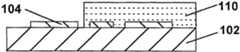
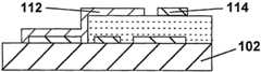
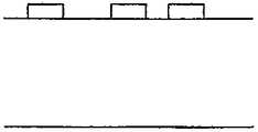
도 2 로부터 액티브 매트릭스 디스플레이의 제조의 당업자에게 당연히 명백 해 지듯이, MEMS 스위치의 존재를 제외하면, 도 2 에 도시된 백플레인은 종래의 트랜지스터-기반 액티브 매트릭스 백플레인과 매우 유사하다. 백플레인은 임의의 주어진 순간에서 행 전극들 (R) 중 오직 하나가 선택되도록 (즉, 거기에 작동 전압이 인가된) 종래의 설계의 행 드라이버 (미 도시) 에 연결되는 복수의 병렬 행 전극 (R) 을 포함하는 반면, 다른 행은 전형적으로 설명한 백플레인으로부터 전기-광학 매체의 반대 면 상에 제공되는 동일한 전압의 단일 공통 전극에 세팅하며, 소정의 간격 후, 원래-선택된 행 전극 (R) 은 선택해제되고, 다음 행 전극 (R) 이 선택되며, 시퀀스 (sequence) 가 각각의 행 전극 (R) 이 주기적인 방법으로 차례로 선택되도록 계속된다. 백플레인은 서로 평행하지만 행 전극들에 대해 수직으로 배열된 열 전극들 (C), 및 도 2 에 도시된 오직 하나인 제 1 또는 픽셀 전극들 (104) 을 더 포함한다. 픽셀 전극들 (104) 은 각각 픽셀 전극이 하나의 행 전극 (R) 과 하나의 열 전극 (C) 의 교차점과 유일하게 연관되도록 직사각형의 어레이에 배열된다. 픽셀 전극들 (104) 는 캔틸레버 빔 (112), 연관된 행 전극 (R) 의 확장의 형태를 가지는 액추에이터 (actuator) (또는 제 2) 전극 (106), 및 연관된 열 전극 (C) 의 확장의 형태를 가지는 소스 (또는 제 3) 전극 (108) 을 포함하는 MEMS 스위치를 통해 그 연관된 열 전극 (C) 에 연결된다. MEMS 스위치에 정통한 당업자에게 명백하듯이, 액추에이터 전극 (106) 상에 작동 전압이 인가되지 않은 상태에서, MEMS 스위치는 소스 전극 (108) 로부터 떨어져 위치한 캔틸레버 빔 (112) 의 자유단 (도 2 에서 도시된 것과 같은 좌측단) 을 개방위치에 유지하며, 따라서 이 픽셀 전극 (104) 과 연관된 열 전극 (C) 사이에 어떠한 전기적 접속이 없게된다. 다만, 행 드라이버가 특정 행을 선택하고 선택된 행 전극 (R) 에 작동 전압을 인가할 때, 작동 전압이 액추에이터 전극 (106) 상에 나타나고, 캔틸레버 빔 (112) 은 그 자유단이 소스 전극 (108) 에 접속하도록 하향으로 끌어당겨지며, 따라서 이 픽셀 전극 (104) 과 연관된 열 전극 (C) 사이에 전기적 접속이 성립하여 연관된 열 전극 (C) 와 동일한 전압에 픽셀 전극 (104) 이 놓이게 한다. 그러므로, 선택된 행의 픽셀 전극들 (즉, 선택된 행 전극 (R) 에 연관된 전극들) 만이 연관된 행 전극 (C) 과 동일한 전압에 놓이게 되고, 디스플레이에 인접하여 위치된 전기-광학 매체의 기록이 종래 트랜지스터-기반 백플레인의 방법과 정확하게 유사한 라인-바이-라인 (line-by-line) 방법으로 진행된다.As will be obvious to those skilled in the art of manufacturing an active matrix display from FIG. 2, except for the presence of a MEMS switch, the backplane shown in FIG. 2 is very similar to a conventional transistor-based active matrix backplane. The backplane comprises a plurality of parallel row electrodes R connected to a row driver (not shown) of conventional design such that only one of the row electrodes R is selected at any given moment (ie, an operating voltage is applied thereto). While the other row is typically set from a described backplane to a single common electrode of the same voltage provided on the opposite side of the electro-optical medium, and after a predetermined interval, the originally-selected row electrode R is selected It is released, the next row electrode R is selected, and the sequence continues so that each row electrode R is selected in turn in a periodic manner. The backplane further comprises column electrodes C parallel to each other but arranged perpendicular to the row electrodes, and only one first or
도 2 에 도시된 백플레인은, 각 픽셀 전극 (104) 에 연관되고, 열 전극 (C) 의 인접한 부분과 함께 캐패시터를 형성하는 캐패시터 전극 (114) 을 더 포함한다.The backplane shown in FIG. 2 further includes a
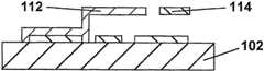
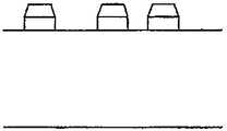
도 2 에 도시된 백플레인을 형성하는데 사용되는 프로세스는 이하 도 1a 내지 도 1d 를 참조하여 설명될 것이다. 도 1a 에 도시된 것처럼, 프로세스는 예를 들어 폴리머막 또는 폴리머-코팅된 금속막일 수 있는 기판 (102) 을 절연하는 단계부터 시작한다. 프로세스의 제 1 단계에서, 얇은 금속층이 기판 (102) 상에 증착되고, 도 1a 에 도시된 구조를 형성하도록 소위 픽셀 전극 (104), "게이트" 또는 액추에이터 전극 (106) 및 소스 전극 (108)인 3개의 전극들을 형성하도록 임의의 편리한 방법으로 패터닝된다. 프로세스의 바람직한 형태에서, 금속층은 약 100 nm 의 두께로 스퍼터 (sputter) 증착함으로써 금 증착된다. 다음으로, 희생층 (110) 은 액추에이터 및 소스 전극들을 커버하지만 노출된 픽셀 전극 (104) 을 남기도록 도 1b 에 도시된 형태로 증착되고, 이 희생층 (110) 은 픽셀 전극 (104) 과 액추에이터 전극 (106) 사이의 간격의 전부가 아닌 일부를 커버한다. 희생층 (110) 은 약 1㎛ 의 두께로 실온에서 스퍼터 증착함으로써 구리 증착하는 것이 바람직하다. 그 후, 희생층은 기계식 캔틸레버 빔의 기저 영역을 정의하고 1 금속 2 기판 캐패시터의 포스트들을 지지하도록 에칭된다. 감광제층은 그 후 캔틸레버 빔 (112) 과 캐패시터 전극 (114) 이 도금되는 개구를 남기도록 부착되고 패터닝되며, 실온 전기도금 용액 및 금과 같은 낮은 스트레스 재료를 사용하는 것이 바람직하다 (캐패시터 전극 (114) 의 위치는 이해를 쉽게하기 위해 도 1a 내지 1d 에서 왜곡되어 도시되었다). 빔 (112) 의 두께는 약 2-4 ㎛ 인 것이 바람직하다. 마지막으로, 감광제층은 도 1c 에 도시된 것처럼 구조를 제공하도록 바람직하게는 습식 화학적 에칭을 사용하여 벗겨지고, 그 후 희생층 (110) 은 제거되며, 그 후 캔틸레버 빔 (112) 을 제거하는 것이 바람직하다.The process used to form the backplane shown in FIG. 2 will now be described with reference to FIGS. 1A-1D. As shown in FIG. 1A, the process starts with insulating the
사용되는 전기-광학 매체의 유형에 따라, MEMS 스위치들과 전기-광학 매체 사이의 물리적 분리를 유지하는 것이 바람직하거나 필수적이고, 이 목적으로 보호 캡슐화층은, 희생층이 제거된 후에 MEMS 스위치가 우연적으로 손상되는 것을 막기위해 백플레인에 부착된다. 도 3 에 도시된 것처럼, 이러한 보호 캡슐화층의 바람직한 형태는 MEMS 스위치에 정렬되고 기판에 접착된 사전-패터닝된 폴리이미드 또는 다른 폴리머 캡슐화제 (116) 를 포함한다.Depending on the type of electro-optic medium used, it is desirable or necessary to maintain physical separation between the MEMS switches and the electro-optical medium, and for this purpose the protective encapsulation layer is accidental after the sacrificial layer is removed. It is attached to the backplane to prevent damage. As shown in FIG. 3, a preferred form of such protective encapsulation layer comprises a pre-patterned polyimide or
본 발명의 MEMS-기반 백플레인은 몇가지 중요한 기술적 이점을 제공한다. MEMS 스위치는 "온 (on)" 상태에서 낮은 임피던스를 가지고 "오프 (off)" 상태에 서 매우 높은 임피던스를 가지므로 탁월한 온/오프 비율을 제공하고, 따라서 다른 유형의 비-선형 구성요소를 통과하는 누설 전류와 관련된 문제를 회피한다. 도 1a-1d 에 참조하여 상술한 것처럼, MEMS 스위치는 오직 3 개 또는 4 개의 마스크들을 사용하는 단일 프로세스에서 제조되고 어떤 높은 온도 프로세싱 단계를 요구하지 않을 수 있다. 그러므로, 프로세스는 예를 들어 폴리(에틸렌 테레프탈레이트) 막 같은 낮은 비용의 가요성 기판 상에서 사용될 수 있다. 또한, 상술한 MEMS 제조 프로세스는 박막 트랜지스터 또는 다이오드에 기초한 백플레인을 제조하는 프로세스들보다 프로세싱 중 환경오염에 덜 민감하여서 요구되는 클린 룸 (clean room) 시설의 비용을 감소시킬 수 있다. 또한, MEMS-기반 백플레인의 제조 프로세스는 몇몇 정련되지 않은 패터닝 단계를 사용할 수 있다.The MEMS-based backplane of the present invention provides several important technical advantages. MEMS switches have low impedance in the "on" state and very high impedance in the "off" state, providing excellent on / off ratios and thus passing through other types of non-linear components. Avoids the problems associated with leakage current. As described above with reference to FIGS. 1A-1D, the MEMS switch may be manufactured in a single process using only three or four masks and may not require any high temperature processing steps. Therefore, the process can be used on low cost flexible substrates such as poly (ethylene terephthalate) films, for example. In addition, the aforementioned MEMS fabrication process is less susceptible to environmental pollution during processing than processes for fabricating backplanes based on thin film transistors or diodes, thereby reducing the cost of clean room facilities required. In addition, the manufacturing process of the MEMS-based backplane may use some unrefined patterning steps.
MEMS 스위치는 매우 작은 선택된 라인 대 픽셀 캐패시턴스를 가지므로, MEMS-기반 백플레인은 유사한 트랜지스터-기반 백플레인 또는 다이오드-기반 백플레인에 비해 이러한 캐패시턴스에 기인한 더 작은 직류 불평형을 가지고, 이 직류 불평형의 감소는 작동 수명 및/또는 전기-광학 매체의 몇몇 유형, 특히 입자-기반 전기영동 매체의 디스플레이 특성을 연장시키는데 중요하다. 또한, MEMS-기반 디스플레이에서 선택 라인과 데이터 라인의 겹치는 영역이 공기에 의해 분리될 수 있기 때문에 (도 1d 및 2 참조), 공기가 거의 정확하게 1 인 유전 상수를 가지므로 이러한 겹치는 영역 당 원하지 않는 캐패시턴스는 절대적인 최소로 유지되고, 큰 비율의 전력 소모가 데이터 라인에 연관된 캐패시턴스의 충전 및 방전에 의한 것으로 설명되므로 감소한 캐패시턴스는 결과적으로 디스플레이의 전력 소모를 감소시 킨다.Since MEMS switches have very small selected line-to-pixel capacitances, MEMS-based backplanes have a smaller direct current unbalance due to these capacitances compared to similar transistor-based or diode-based backplanes, and this reduction in direct current unbalance It is important to extend the lifetime and / or display characteristics of some types of electro-optical media, in particular particle-based electrophoretic media. Also, in MEMS-based displays, since the overlapping areas of the select and data lines can be separated by air (see FIGS. 1D and 2), air has an almost constant dielectric constant of 1, so unwanted capacitance per such overlapping area. Is kept at an absolute minimum, and the reduced capacitance reduces the power consumption of the display as a large percentage of power consumption is explained by the charging and discharging of the capacitance associated with the data line.
본 발명의 MEMS-기반 백플레인의 변형된 형태에서, 도 1d, 2 및 3 에 도시된 것 같은 캔틸레버 빔은 캔틸레버 빔 보다 긴장을 받을 가능성이 적은, MEMS 격판 (diaphragm) 으로 교체될 수 있다.In a modified form of the MEMS-based backplane of the present invention, cantilever beams such as those shown in FIGS. 1D, 2 and 3 can be replaced with MEMS diaphragms, which are less likely to be strained than cantilever beams.
파트part B: 본 발명의 B: of the present invention엠보싱Embossing 프로세스 process
상술한 것처럼, 백플레인의 제조는 기판 상에 작은 피쳐들 (feature) 의 패터닝을 수반한다. 표 1 에 나타난 것처럼, 다양한 패터닝 응용에서 요구하는 임계 치수 길이 스케일들이 있고, 기술의 범위는 이러한 치수들을 성공적으로 달성하도록 사용되어 왔다.As mentioned above, fabrication of a backplane involves the patterning of small features on a substrate. As shown in Table 1, there are critical dimension length scales required in various patterning applications, and a range of techniques have been used to successfully achieve these dimensions.
표 1: 미세한 피쳐를 패터닝하는 다양한 기술에 사용되는 프로세스들Table 1 : Processes Used in Various Techniques for Patterning Fine Features
또한 상술한 것처럼, 소위 25 ㎛ 미만인 임계치수를 가지는 매우 작은 피쳐를 제조하도록, 포토리소그래피 (photolithography) 는 주요기술로서 명백하게 나타났다. 최근 몇십년 동안 광범위한 연구로 인해, 포토리소그래피 기술은 0.13 ㎛ 프로세스가 풀-스케일 제조에 있고 0.10 ㎛ 프로세스가 연구 중에 있게 되기까 지 개선되어 왔다. 포토리소그래피는 자체로 큰 스케일의 산업적 응용이 가능한 규모 있는 기술로서 증명되어 왔지만, 일반적으로 많은 개수의 프로세스 단계와 포토리소그래피 제조 장비와 연관된 값비싼 자본 비용으로 인해 비싸다고 인식된다.As also mentioned above, photolithography has been clarified as a major technique to produce very small features having a critical dimension of less than 25 μm. Due to extensive research in recent decades, photolithography techniques have been improved until 0.13 μm processes are in full-scale manufacturing and 0.10 μm processes are under study. Photolithography has proven itself as a scaleable technology for large scale industrial applications, but it is generally recognized as expensive due to the large number of process steps and the expensive capital costs associated with photolithographic manufacturing equipment.
상술한 것처럼, 본 발명의 제 2 양태는 백플레인의 부품과 다른 전자 소자들을 패턴화하도록, 소위 엠보싱된 레지스트 프로세스인 대안적 패터닝 기술의 사용에 관한 것이다. 엠보싱된 레지스트 프로세스는 종래 포토리소그래피 프로세스 에 대해서 여러 이점을 제공하고, 높은 롤-투-롤 (roll-to-roll) 프로세싱 처리율, 1 ㎛ 보다 작은 피쳐 크기, 및 감소된 고정 또는 변동 비용을 가능하게 한다.As mentioned above, a second aspect of the present invention relates to the use of an alternative patterning technique, a so-called embossed resist process, to pattern components and other electronic components of the backplane. Embossed resist processes offer several advantages over conventional photolithography processes and allow for high roll-to-roll processing throughput, feature sizes smaller than 1 μm, and reduced fixed or variable costs. do.
첨부된 도면 중 도 4a-4e 는 본 발명의 엠보싱 프로세스를 도시한다. 도 4a 에 도시된 것처럼, 기판 (402) 은 먼저 패터닝되는 재료 (404) 로 코팅되며, 이 재료는 금속, 절연체, 반도체 또는 다른 유형의 패터닝 가능 재료일 수 있다. 다음으로 엠보싱 가능 재료층은 (이하 편리하게 "레지스트 (resist)" 라 함; 406) 재료 (404) 상에 부착되고, 레지스트는 레지스트에 대한 조직 (texture) 또는 패턴을 전하도록 "마스터 스탬프 (master stamp)" (도 4a 에서 도시된 것처럼, 엠보싱된 롤러 (408) 의 형태가 바람직함) 를 사용하여 엠보싱된다. 도 4b 에서 가장 잘 보이는, 이 엠보싱 단계는 레지스트 (406) 를 두꺼운 (제 2) 영역들 (406A) 및 얇은 (제 1) 영역들 (406B) 로 성형하고, 2 개의 영역들 사이의 레지스트 (406) 의 분할은 롤러 (408) 의 패터닝으로써 임의의 바람직한 방법으로 사전결정된다.4A-4E of the accompanying drawings show an embossing process of the present invention. As shown in FIG. 4A, the
프로세스의 다음 단계에서, 패터닝된 레지스트는 얇은 영역들 (406B) 을 제 거하고 그 위에 위치한 재료 (404) 를 노출하도록 충분한 정도로 (반도체 제조 기술의 당업자에게 잘 알려진 종래의 에칭 프로세스 중 하나를 사용하여) 약하게 에칭되는 반면, 재료 (404) 의 잔여 부분들은 두꺼운 영역 (406A) 에 의해 여전히 커버되어서, 도 4c 에 도시된 구조를 제조한다. 그 후, 기판은 바람직한 정도로 재료 (404) 의 노출된 부분들을 에칭하는 제 2 에칭 공정을 받으므로, 도 4d 에 도시된 구조를 제조하고, 마지막으로 레지스트는 기판 (402) 상에 최종 패터닝된 재료 (404) 를 남기도록 도 4 에 도시된 것처럼 기판으로부터 벗겨진다.In the next step of the process, the patterned resist is sufficiently removed to remove the
표면에 부착되는 엠보싱 가능 재료는 패터닝 단계를 최적화하도록 선택될 수 있다. 상용화된 감광제는 엠보싱 가능 재료로서 사용될 수 있다. 감광제는 그 유리 전이 온도 (Tg) 를 초과하는 온도에서 엠보싱될 수 있고, 밑에 있는 재료를 노출하도록 습식 또는 건식 에칭될 수 있다. 레지스트는 밑에 있는 재료를 에칭하도록 사용된 화학 반응에 저항하고 밑에 있는 재료의 패터닝 후 그 표면으로부터 쉽게 벗겨지도록 선택될 수 있다. 몇몇의 경우에서, 레지스트의 엠보싱 전에 그로부터 용매를 제거하도록 레지스트를 "소프트 베이킹" 하는 것이 필요하거나 바람직하다. 또한, 몇몇의 경우에서, 레지스트가 밑에 있는 재료의 에칭을 견딜 수 있는 것을 보증하도록 얇은 영역 (406B) 을 제거하는 에칭 후 레지스트를 "하드 베이킹" 하는 것이 바람직할 수 있다.The embossable material attached to the surface can be selected to optimize the patterning step. Commercially available photosensitizers can be used as embossable materials. The photosensitizer can be embossed at a temperature above its glass transition temperature (Tg) and can be wet or dry etched to expose the underlying material. The resist can be selected to resist chemical reactions used to etch the underlying material and to easily peel off from its surface after patterning of the underlying material. In some cases, it is necessary or desirable to "soft bake" the resist to remove solvent therefrom before embossing the resist. Also, in some cases, it may be desirable to "hard bake" the resist after etching to remove
용융된 재료 (폴리머 외) 는 엠보싱 재료 또는 레지스트로서 사용될 수 있다. 예를 들어, 왁스성 (waxy) 재료 (예를 들어, 옥타코사인, 논아데카인, 등의 알칸) 가 사용될 수 있다. 이러한 왁스성 재료는 가열된 슬롯 다이, 음각 (intaglio) 플레이트, 스핀 코팅 척 (chuck), 오프셋 프린팅 롤러, 또는 당업자에게 알려진 다른 유사한 장치를 사용하여 액상으로 코팅될 수 있다. 용융된 재료는 전형적으로 증착되는 것처럼 얇은 엠보싱 가능 막으로 응고될 것이고, 그 다음 습식 또는 건식 에칭 기술을 사용하여 엠보싱되고 에칭될 수 있다. 패터닝된 레지스트막은 밑에 있는 재료에 대해 에칭 마스크로서 기능하고, 상술한 것처럼, 밑에 있는 재료의 에칭의 결과로, 벗겨진다. 헥산과 같은 용매가 상기 왁스성 재료를 효과적으로 벗겨내고, 증착 후에 레지스트로부터 용매를 건조하는 것이 필요하지 않기 때문에 이러한 프로세스는 이점이 있다. 또한, 사용되는 화학 물질들의 적절한 선택 ("튜닝 (tuning)") 으로, 비교적 비-독성 용매가 패터닝이 완료된 후 밑에 있는 재료로부터 왁스성 재료를 벗겨내도록 사용될 수 있다.The molten material (other than the polymer) can be used as embossing material or resist. For example, waxy materials (eg alkanes such as octacosine, non-adecaine, etc.) can be used. Such waxy materials may be coated in a liquid phase using heated slot dies, intaglio plates, spin coating chucks, offset printing rollers, or other similar devices known to those skilled in the art. The molten material will typically solidify into a thin embossable film as it is deposited and then can be embossed and etched using wet or dry etching techniques. The patterned resist film functions as an etching mask for the underlying material and, as described above, is peeled off as a result of etching of the underlying material. This process is advantageous because a solvent such as hexane effectively strips off the waxy material and does not require drying the solvent from the resist after deposition. In addition, with proper selection of the chemicals used (“tuning”), a relatively non-toxic solvent can be used to strip the waxy material from the underlying material after the patterning is complete.
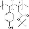
예를 들어, 도 5a 에 도시된 4-하이드록시스틸렌 (4-hydroxystryrene) 및 부틸-메타아크릴레이트 (butyl-methacrylate) 의 공중합체와 같은 엠보싱된-레지스트 개념에 대해 튜닝된 공중합체가 사용될 수 있다. 이 블록 공중합체의 4-하이드록시스틸렌 화합물은 기저 용액이고, 공중합체는 산에서 블록이 해제된다. 결과적으로, 공중합체는 엠보싱되는 레지스트 프로세스에서 몇몇의 유익한 특성들을 나타낸다. 먼저, 폴리머 분자량의 조정은 폴리머의 유리 전이 온도가 허용되는 엠보싱 온도 범위인 약 100 부터 약 150℃ 까지의 범위 내에서 조정되어지도록 한다. 두번째로, 약 기저 용매는 패터닝된 공중합체를 다시 에칭하도록 사용될 수 있으므로, 이로써 밑에 있는 재료를 노출한다. 가장 공통인 밑에 있는 재료 (금속, 반도체, 절연체) 를 에칭하는데 사용되는 산은 밑에 있는 재료의 에칭 중에 공중합체를 블록 해제시킬 것이고, 그러므로 에칭이 종료된 후 레지스트의 용이한 제거를 가능하게 한다.For example, a copolymer tuned to the embossed-resist concept, such as the copolymer of 4-hydroxystryrene and butyl-methacrylate, shown in FIG. 5A can be used. . The 4-hydroxystyrene compound of this block copolymer is a base solution, and the copolymer is unblocked in an acid. As a result, the copolymer exhibits some beneficial properties in the resist process that is embossed. First, the adjustment of the polymer molecular weight is such that the glass transition temperature of the polymer is adjusted within a range from about 100 to about 150 ° C., which is an acceptable embossing temperature range. Secondly, a weak base solvent can be used to etch the patterned copolymer again, thereby exposing the underlying material. Acids used to etch the most common underlying materials (metals, semiconductors, insulators) will unblock the copolymer during etching of the underlying materials, thus allowing for easy removal of the resist after the etching is finished.
다른 방법으로, 도 5b 에 도시된 메타아크릴레이트-기반 블록은 엠보싱된 레지스트 공중합체에서 도 5a 에 도시된 부틸 메타아크릴레이트 블록를 대신하여 사용된다. 이 상이한 블록의 사용은 약 175 내지 180℃ 의 온도에서 엠보싱된 레지스트가 열로 블록 해제되는 것을 가능하게 한다. 열 블록 해제는, 패터닝되는 밑에 있는 재료가 상술한 종래의 산 에칭 화학반응을 이용하여 에칭되지 않는 경우에, 유용한 다른 방법이다.Alternatively, the methacrylate-based block shown in FIG. 5B is used in place of the butyl methacrylate block shown in FIG. 5A in the embossed resist copolymer. The use of this different block allows the embossed resist to unblock with heat at a temperature of about 175 to 180 ° C. Thermal blocking is another method that is useful when the underlying material being patterned is not etched using the conventional acid etch chemistry described above.
본 발명의 프로세스에서 엠보싱 공정을 수행하는데 사용되는 마스터 스탬프는 다양한 종래 기술인 마이크로제조 기술을 사용하여 제작될 수 있다. 바람직하게는, 마스터 스탬프는 컴팩트 디스크 (CD) 및 DVD 의 제조 용 니켈 마스터 스탬프를 만드는 컴팩트 디스크 제작자에 의해 공통적으로 사용되는 기술을 사용하여 만들어진다. 이 기술들은 포토리소그래피적인 미세 템플레이트의 형성을 요구되며, 반면에 니켈 마스터 스탬프는 전기주조된다.The master stamp used to perform the embossing process in the process of the present invention can be produced using various conventional microfabrication techniques. Preferably, the master stamp is made using a technique commonly used by compact disc producers to make nickel master stamps for the production of compact discs (CDs) and DVDs. These techniques require the formation of photolithographic fine templates, while nickel master stamps are electroformed.
CD 및 DVD 마스터 프로세스로부터 생긴 니켈 포일은 본 발명에서 사용되는데 아주 적합하며, 다만 몇몇의 종래 CD/DVD 프로세스의 변형이 요구된다. 먼저, CD 상의 피트는 일반적으로 250 ㎚ 깊이보다 낮지만, 본 발명에서는, 정교한 자국 (imprint) 을 달성하도록 스탬프 피쳐는 일반적으로 100 내지 1000㎚의 차수인 레지스트 두께보다 약 2 내지 5 배 깊을 수 있기 때문에, 1 내지 10 ㎛ 깊이의 차수의 마스터 스탬프 상에 피쳐를 만드는 것이 일반적으로 바람직하다.Nickel foils resulting from CD and DVD master processes are well suited for use in the present invention, but require modification of some conventional CD / DVD processes. First, the pits on the CD are generally less than 250 nm deep, but in the present invention, the stamp feature can be about 2 to 5 times deeper than the resist thickness, which is typically on the order of 100 to 1000 nm, to achieve a fine imprint. It is generally desirable to create features on master stamps of
마스터 상에 이러한 깊은 피쳐를 제조하기 위해, 두꺼운 막 프로세싱에 최적화된 감광제는 마스터 제조 중에 사용되어야 한다. 예를 들어, SU-8 레지스트는 100㎛ 이상의 두께로 막을 제조하도록 사용될 수 있다. 템플레이트로부터 니켈 마스터의 용이한 해제를 보장하기 위해서, 마스터의 피쳐 상에 경사진 측벽들을 세우는 것이 바람직하다. 경사진 측벽 기술은 높은 처리율의 약품 발견 시스템을 복제하는데 사용되는 마스터를 형성하는데 이용되었지만, 명백하게 엠보싱된 레지스트 프로세스에서 사용되어오지 않았다.In order to fabricate such deep features on the master, photosensitizers optimized for thick film processing must be used during master fabrication. For example, SU-8 resist can be used to make a film with a thickness of 100 μm or more. In order to ensure easy release of the nickel master from the template, it is desirable to erect sloped sidewalls on the feature of the master. Inclined sidewall technology has been used to form masters used to replicate high throughput drug discovery systems, but has not been used in apparently embossed resist processes.
마스터 스탬프 상의 몇몇 기하 피쳐들 때문에, 발전된 MEMS 장치의 제조에서 평범하게 행해지는 것처럼, 바람직한 피쳐들을 가진 유리 웨이퍼 또는 유리 기판을 에칭하도록 예를 들어 반작용 이온 에칭 (RIE; reactive ion etching) 또는 레이저 침식과 같은 대안적 기술이 이용되는 것이 유용할 수 있다.Because of some geometrical features on the master stamp, for example, reactive ion etching (RIE) or laser erosion to etch a glass wafer or glass substrate with desirable features, as is commonly done in the manufacture of advanced MEMS devices. It may be useful to use such alternative techniques.
본 발명의 엠보싱 프로세스는 패터닝 재료에 대한 종래의 포토리소그래피 기술에서 몇몇의 독특한 이점을 제공한다. 엠보싱 프로세스는, 기계적 엠보싱 기구를 가진 종래의 리소그래피 UV 노광 기구, 및 값 싸고 화학적으로 단순한 재료들을 가진 종래의 감광제로 대체되기 때문에 리소그래피보다 낮은 고정 비용 및 변동 비용을 약속한다. 본 발명의 엠보싱 프로세스는 발전된 포토리소그래피 프로세스에서 달성될 수 있는 것보다 5 내지 10 배 작은, 특징적인 치수에서 6 내지 10 ㎚ 만큼 작은 피쳐들을 달성하도록 나타내어졌다. 용융된 폴리머 레지스트를 이용한 본 발명의 실시형태를 사용할 때, 포토리소그래피에서 요구되는 소프트 및 하드 베이킹 단계는 완전히 제거된다. 미크론 스케일보다 작은 피쳐 사이즈에 서, 엠보싱된 레지스트 프로세스는 모두 습식 프로세싱을 사용하여 성공적으로 완성되며, 즉 어떠한 값비싼 진공 공정들도 요구되지 않는다. 마지막으로, 엠보싱된 레지스트 프로세스는 도 4a 에 도시된 것처럼 마스터 스탬프로서 롤러를 사용하여 높은 처리율의 롤-투-롤 패터닝에 매우 적합하다.The embossing process of the present invention provides several unique advantages over conventional photolithography techniques for patterning materials. The embossing process promises lower fixed costs and variable costs than lithography because it is replaced by conventional lithography UV exposure apparatuses with mechanical embossing mechanisms and conventional photosensitizers with cheap and chemically simple materials. The embossing process of the present invention has been shown to achieve features as small as 6 to 10 nm in characteristic dimensions, 5 to 10 times smaller than can be achieved in advanced photolithography processes. When using embodiments of the invention with molten polymer resist, the soft and hard baking steps required for photolithography are completely eliminated. At feature sizes smaller than the micron scale, the embossed resist processes are all successfully completed using wet processing, ie no expensive vacuum processes are required. Finally, the embossed resist process is well suited for high throughput roll-to-roll patterning using rollers as master stamps as shown in FIG. 4A.
파트part C: 매몰된 트랜지스터 C: buried transistor백플레인Backplane
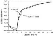
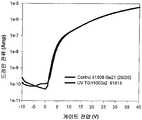
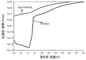
상술한 것처럼, 전기-광학 디스플레이의 제조에서, 디스플레이의 백플레인과 전면 부분은 일반적으로 분리된 유닛으로서 제조되고 최종 디스플레이를 제작하도록 함께 적층된다. 이러한 적층은 일반적으로 백플레인을 디스플레이의 전면 부분에 접착하도록 적층 접착제의 사용이 요구된다. 따라서, 최종 디스플레이에서, 제조된 것처럼 백플레인의 노출된 표면이 적층 접착제에 노출되고, 많은 경우에 적층 접착제는 백플레인의 노출된 표면상의 트랜지스터 또는 다른 비-선형 소자들의 성능에 해롭게 영향을 미칠 수 있는 재료들을 포함한다. 예를 들어, 비정형 실리콘 TFT의 채널에 특정 상용 폴리우레탄 적층 접착제의 직접적인 응용은 실질적으로 트랜지스터를 파괴하는 것으로 알려져 왔으며, 첨부된 도면들 중 도 6 에 도시된 것처럼, 하나의 이러한 실험에서, 트랜지스터의 온/오프 비율이 106 에서 약 10 으로 감소되는 것이 알려졌다. 또한, 몇몇 유형의 전기-광학 매체는 적층 접착제을 통해 이동할 수 있어서 트랜지스터 또는 다른 비-선형 소자에 악 영향을 미칠 수 있는 이동성 종 (species) 을 포함한다. 예를 들어, 입자-기반 전기영동 매체는 이 방법으로 이동할 수 있고 비정형 실리콘 트랜지스터의 특성에 영향을 미칠 수 있는 하이드로카본 (hydrocarbon) 용액을 포함한다. 마지막으 로, 비정형 실리콘 TFT 는 또한 전기-광학 매체를 통해 TFT에 유입될 수 있는 광 또는 습기에 의해 손상될 수도 있으며, 캡슐화 입자-기반 전기영동 매체와 같은 많은 전기-광학 매체는 정상적으로는 불투명하게 여겨지지만, 약간의 광은, 예를 들어, 캡슐들 사이의 작은 간격을 통해, 이러한 매체에 침투한다.As mentioned above, in the manufacture of electro-optical displays, the backplane and front portion of the display are generally manufactured as separate units and stacked together to produce the final display. Such lamination generally requires the use of a lamination adhesive to adhere the backplane to the front portion of the display. Thus, in the final display, the exposed surface of the backplane, as manufactured, is exposed to the stacking adhesive, and in many cases the stacking adhesive is a material that can adversely affect the performance of transistors or other non-linear devices on the exposed surface of the backplane. Include them. For example, the direct application of certain commercial polyurethane laminate adhesives to the channels of amorphous silicon TFTs has been known to substantially destroy transistors, and in one such experiment, as shown in FIG. It is known that the on / off ratio is reduced from 106 to about 10. In addition, some types of electro-optical media include mobile species that can migrate through the lamination adhesive and can adversely affect transistors or other non-linear devices. For example, particle-based electrophoretic media include hydrocarbon solutions that can be moved in this manner and can affect the properties of amorphous silicon transistors. Finally, atypical silicon TFTs may also be damaged by light or moisture that may enter the TFT through the electro-optical medium, and many electro-optical media, such as encapsulated particle-based electrophoretic media, are normally opaque. Though considered, some light penetrates this medium, for example, through a small gap between the capsules.
이러한 문제를 회피하기 위해서, 비-선형 소자들과 전기-광학 매체 사이에 장벽 또는 보호층을 삽입하는 것이 알려져 있다. 예를 들어, 상기한 제 2002/0119584 호는 소위 "매몰된 트랜지스터 설계"를 가지는 백플레인을 설명한다. 이러한 설계에서, 픽셀 전극만이 적층 전에 최종 백플레인의 표면 상에서 노출되며, 백플레인의 트랜지스터는, 트랜지스터의 드레인들이 보호층을 통과하는 도전성 비아들에 의해 연관된 픽셀 전극들과 접속된채, 보호층 하에 "매몰된다". 상기한 공개된 출원에서 설명되는 것처럼 이 설계의 바람직한 형태에서, 보호층은 플라즈마 개선된 화학적 기상 증착 (PECVD; plasma enhanced chemical vapor deposition) 에 의해 증착된 약 5 ㎛ 이상의 실리콘 실화물을 포함하고, 이 상대적으로 두꺼운 층은 트랜지스터들의 채널들과 데이터 라인들 모두를 커버하여야 한다. 이러한 두꺼운 질화물막을 크랙킹 (cracking) 없이 증착하는 것은 불가능하지는 않지만 어렵다. 따라서, 보호막으로서 실리콘 질화막을 대체하는 대안적인 재료를 찾는 것이 바람직하다.To avoid this problem, it is known to insert a barrier or protective layer between the non-linear elements and the electro-optical medium. For example, the above-mentioned 2002/0119584 describes a backplane with a so-called "embedded transistor design". In this design, only the pixel electrode is exposed on the surface of the final backplane prior to lamination, and the transistor of the backplane is under the protective layer, with the drains of the transistor connected with associated pixel electrodes by conductive vias passing through the protective layer. Buried ". In a preferred form of this design, as described in the published application above, the protective layer comprises at least about 5 μm silicon silicide deposited by plasma enhanced chemical vapor deposition (PECVD), The relatively thick layer should cover both the channels and the data lines of the transistors. Deposition of such thick nitride films without cracking is not impossible but difficult. Therefore, it is desirable to find an alternative material to replace the silicon nitride film as a protective film.
에폭시, 폴리우레탄, 실리콘, 폴리아크릴레이트, 및 폴리이미드 폴리머는 트랜지스터 또는 전기-광학 디스플레이에서 사용되는 백플레인의 다른 비-선형 소자를 캡슐화하고 보호하도록 보호막으로서 실리콘 질화물을 대신하여 사용될 수 있 다. 바람직한 폴리머는 PECVD 보다 훨씬 덜 복잡하고 적은 장비를 요구하는 프로세스인, 스크린 프린팅에 의해 백플레인에 부착될 수 있다.Epoxy, polyurethane, silicone, polyacrylates, and polyimide polymers can be used in place of silicon nitride as a protective film to encapsulate and protect other non-linear elements of the backplane used in transistors or electro-optical displays. Preferred polymers can be attached to the backplane by screen printing, a process that is much less complex and requires less equipment than PECVD.
본 발명에 사용된 폴리머 캡슐화제는 열 또는 방사 (radiation) 중 어느 하나에 의해 경화될 수 있으며, 바람직하게는 자외선 방사에 의한다. 바람직한 열 경화 재료는 Epoxy Technology 의 EpoTek H70E-2LC 와 DuPont Electronic Materials 의 DuPont 5036 를 포함한다. 바람직한 UV 경화 재료는 Allied Photochemical Inc. 의 TGH 1003x2 와 Creative Materials Inc. 의 CM116-20 를 포함한다. 이러한 재료들의 특성 및 경화 조건은 아래의 표 2 에서 요약된다.The polymer encapsulating agent used in the present invention may be cured by either heat or radiation, preferably by ultraviolet radiation. Preferred thermal curing materials include EpoTek H70E-2LC from Epoxy Technology and
표 2 :폴리머 재료들Table 2 : Polymer Materials
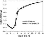
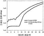
이 재료들은 상기한 제 2002/0019081 호에서 설명한 것처럼 실질적으로 폴리이미층으로 코팅된 스테인리스 스틸막 상에 제조된 비정형 실리콘 TFT 를 이용하여 테스트되었다. 20-180 ㎛ 의 직경을 가진 캡슐화제 드롭 (drop) 이 프로브 스테이션 (probe station) 을 이용하여 TFT 의 채널 영역 상에 부착되었다. 열 경화성 코팅은 표 2 의 기재된 것과 같이 요구되는 조건에서 보통의 오븐 (oven) 에서 경화되었다. UV 경화성 코팅에 대해서는, ELC-4000 광 경화 장치 (Light Curing Unit) 가 1-2 분의 경화 시간동안 사용되었다. 캡슐제의 경화 다음으 로, TFT의 전류/전압 곡선이 종래의 형태대로 생성되었고, 결과는 개별적으로 도 7-10 에 도시되었다. 비교하면, 도 11 은 EpoTek H62 (EpoTek H70E-2LC와 동일한 제조사의 열 경화성 폴리머) 로 캡슐화된 TFT 와 유사한 곡선을 나타내는 반면, 도 12 는 Electrodag 452SS (Acheson Industries, Inc. 의 UV 경화성 폴리머) 로 캡슐화된 TFT 와 유사한 곡선을 나타낸다.These materials were tested using an amorphous silicon TFT fabricated on a stainless steel film coated with a polyimide layer substantially as described in 2002/0019081, supra. An encapsulant drop having a diameter of 20-180 μm was deposited on the channel region of the TFT using a probe station. The thermosetting coating was cured in a normal oven at the required conditions as described in Table 2. For UV curable coatings, an ELC-4000 Light Curing Unit was used for a curing time of 1-2 minutes. Curing of the Capsule Next, the current / voltage curve of the TFT was generated in the conventional form, and the results are individually shown in FIGS. 7-10. In comparison, FIG. 11 shows a curve similar to TFT encapsulated with EpoTek H62 (a thermosetting polymer from the same manufacturer as EpoTek H70E-2LC), while FIG. 12 is encapsulated with Electrodag 452SS (UV curable polymer from Acheson Industries, Inc.). Curve similar to that of a TFT.
도 7-10 은 위의 표 2 에 기재된 재료들이 모두 좋은 결과를 주는 것을 나타낸다. 오프 전류는 DuPont 5036 로 캡슐화 한 후 낮아진다. TFT 성능은, EpoTek H70E-2LC 가 캡슐화제로서 사용될 때와 동일하게 유지된다. TGH 1003x2 코팅된 TFT 는 제어 소자에 비교하여 동일한 성능을 가진다. CM 116-20 캡슐화된 TFT 는 제어 소자에 비해 나은 서브-임계 (sub-threshold) 기울기를 가진다. 그러나, 도 11 및 12 는 잘못된 캡슐화제가 선택된 경우 무엇이 일어날 수 있는지를 나타낸다. 도 11 은 비정형 실리콘 TFT 가 EpoTek H62 에 의해 캡슐화된 때, 대부분 손상되는 것을 나타내는 반면, 도 12는 TFT 가 Electrodag 452SS 에 의해 캡슐화된 때, 손상되는 것과 TFT 가 높은 오프 전류를 가지고, 더 누설된다는 것을 나타낸다.7-10 show that the materials listed in Table 2 all give good results. Off current is lowered after encapsulation with
따라서, 본 발명은 트랜지스터 및 전기-광학 디스플레이의 백플레인에 사용되는 다른 비-선형 소자의 보호에 대해 낮은 비용의 프로세스를 제공한다. 사용되는 폴러머 캡슐화제는 상술한 종래 기술의 프로세스에서 사용되는 RECVD 실리콘 질화물 증착 및 포토리소그래피 패터닝 프로세스와 비교하여 낮은 비용의 프로세스인, 스크린 프린팅에 의해 증착되고 패터닝된다.Thus, the present invention provides a low cost process for the protection of transistors and other non-linear devices used in the backplane of electro-optic displays. The polymer encapsulant used is deposited and patterned by screen printing, a lower cost process compared to the RECVD silicon nitride deposition and photolithography patterning processes used in the prior art processes described above.
본 발명의 다양한 양태는 캡슐화된 입자-기반의 전기영동 매체에 관련하여 그 사용에 관하여 주로 상술되었지만, 위에서 언급한 전기-광학 매체의 어느 유형도 본 발명의 전기-광학 디스플레이로서 사용될 수 있다.While various aspects of the present invention have been primarily described above in terms of their use in connection with encapsulated particle-based electrophoretic media, any type of electro-optical media mentioned above may be used as the electro-optical display of the present invention.
첨부된 도면 중 도 1a 내지 1d 는 단일 마이크로전자기계식 스위치를 포함하는 본 발명의 MEMS 백플레인의 부분의 백플레인의 제조 중 다양한 단계에서 취해진 개략적인 측면도이다.1A-1D of the accompanying drawings are schematic side views taken at various stages during the manufacture of a backplane of a portion of a MEMS backplane of the present invention comprising a single microelectromechanical switch.
도 2 는 도 1d 에 도시된 완성된 백플레인의 부분의 평면도이다.FIG. 2 is a plan view of a portion of the completed backplane shown in FIG. 1D.
도 3 은 보호 캡슐화층이 제공되는 본 발명의 개조된 MEMS 백플레인의 부분을 도시하는, 도 1d 의 측면도와 유사한 개략적인 측면도이다.3 is a schematic side view similar to the side view of FIG. 1D showing a portion of the modified MEMS backplane of the present invention provided with a protective encapsulation layer.
도 4a 내지 도 4e 는 본 발명의 엠보싱 프로세스의 다양한 단계를 도시하는 개략적인 측면도이다.4A-4E are schematic side views illustrating various steps of the embossing process of the present invention.
도 5a 는 본 발명의 엠보싱 프로세스에서 사용되는 바람직한 폴리머의 구조식을 도시한다.5A shows the structural formula of a preferred polymer used in the embossing process of the present invention.
도 5b 는 도 5a 에서 도시된 메타아크릴레이트 반복 유닛을 대신할 수 있는 다른 메타아크릴레이트 반복 유닛의 구조식을 도시한다.FIG. 5B shows the structural formula of another methacrylate repeating unit that may replace the methacrylate repeating unit shown in FIG. 5A.
도 6 내지 12 는 본 발명의 매몰된 트랜지스터 백플레인에 사용되도록 의도된 다양한 내장 트랜지스터에 대한 전류/게이트 전압 곡선, 및 특정 제어 실험들에 대한 유사한 곡선들이다.6-12 are current / gate voltage curves for various embedded transistors intended for use in the buried transistor backplane of the present invention, and similar curves for specific control experiments.
*도면의 주요 부호에 대한 설명*Description of the main symbols in the drawing
104; 픽셀 전극 106; 엑추에이터 전극104;
108; 소스 전극 112; 캔틸레버 빔108;
114; 캐패시터 전극 406; 레지스트114;
Claims (8)
Translated fromKoreanApplications Claiming Priority (2)
| Application Number | Priority Date | Filing Date | Title |
|---|---|---|---|
| US31978602P | 2002-12-16 | 2002-12-16 | |
| US60/319,786 | 2002-12-16 |
Related Parent Applications (1)
| Application Number | Title | Priority Date | Filing Date |
|---|---|---|---|
| KR1020057011155ADivisionKR20050086917A (en) | 2002-12-16 | 2003-12-16 | Backplanes for electro-optic displays |
Publications (2)
| Publication Number | Publication Date |
|---|---|
| KR20080049144A KR20080049144A (en) | 2008-06-03 |
| KR100937613B1true KR100937613B1 (en) | 2010-01-20 |
Family
ID=32680696
Family Applications (2)
| Application Number | Title | Priority Date | Filing Date |
|---|---|---|---|
| KR1020087011300AExpired - Fee RelatedKR100937613B1 (en) | 2002-12-16 | 2003-12-16 | Backplanes for Electro-Optical Displays |
| KR1020057011155ACeasedKR20050086917A (en) | 2002-12-16 | 2003-12-16 | Backplanes for electro-optic displays |
Family Applications After (1)
| Application Number | Title | Priority Date | Filing Date |
|---|---|---|---|
| KR1020057011155ACeasedKR20050086917A (en) | 2002-12-16 | 2003-12-16 | Backplanes for electro-optic displays |
Country Status (7)
| Country | Link |
|---|---|
| US (2) | US7365733B2 (en) |
| EP (1) | EP1573389B1 (en) |
| JP (3) | JP2006510066A (en) |
| KR (2) | KR100937613B1 (en) |
| CN (2) | CN1726428A (en) |
| AU (1) | AU2003299673A1 (en) |
| WO (1) | WO2004059378A2 (en) |
Families Citing this family (303)
| Publication number | Priority date | Publication date | Assignee | Title |
|---|---|---|---|---|
| US7999787B2 (en) | 1995-07-20 | 2011-08-16 | E Ink Corporation | Methods for driving electrophoretic displays using dielectrophoretic forces |
| US7411719B2 (en) | 1995-07-20 | 2008-08-12 | E Ink Corporation | Electrophoretic medium and process for the production thereof |
| US7193625B2 (en) | 1999-04-30 | 2007-03-20 | E Ink Corporation | Methods for driving electro-optic displays, and apparatus for use therein |
| US7848006B2 (en) | 1995-07-20 | 2010-12-07 | E Ink Corporation | Electrophoretic displays with controlled amounts of pigment |
| US7327511B2 (en) | 2004-03-23 | 2008-02-05 | E Ink Corporation | Light modulators |
| US8139050B2 (en) | 1995-07-20 | 2012-03-20 | E Ink Corporation | Addressing schemes for electronic displays |
| US7583251B2 (en) | 1995-07-20 | 2009-09-01 | E Ink Corporation | Dielectrophoretic displays |
| US8040594B2 (en) | 1997-08-28 | 2011-10-18 | E Ink Corporation | Multi-color electrophoretic displays |
| DE69920228T2 (en) | 1998-07-08 | 2005-01-27 | E-Ink Corp., Cambridge | METHOD FOR IMPROVING COLOR REPRODUCTION IN ELECTROPHORETIC DEVICES USING MICROCAPSULES |
| US7119772B2 (en) | 1999-04-30 | 2006-10-10 | E Ink Corporation | Methods for driving bistable electro-optic displays, and apparatus for use therein |
| US8115729B2 (en) | 1999-05-03 | 2012-02-14 | E Ink Corporation | Electrophoretic display element with filler particles |
| US7119759B2 (en) | 1999-05-03 | 2006-10-10 | E Ink Corporation | Machine-readable displays |
| US8009348B2 (en) | 1999-05-03 | 2011-08-30 | E Ink Corporation | Machine-readable displays |
| US7893435B2 (en) | 2000-04-18 | 2011-02-22 | E Ink Corporation | Flexible electronic circuits and displays including a backplane comprising a patterned metal foil having a plurality of apertures extending therethrough |
| AU2002250304A1 (en) | 2001-03-13 | 2002-09-24 | E Ink Corporation | Apparatus for displaying drawings |
| US8390918B2 (en) | 2001-04-02 | 2013-03-05 | E Ink Corporation | Electrophoretic displays with controlled amounts of pigment |
| US7679814B2 (en) | 2001-04-02 | 2010-03-16 | E Ink Corporation | Materials for use in electrophoretic displays |
| US20050156340A1 (en) | 2004-01-20 | 2005-07-21 | E Ink Corporation | Preparation of capsules |
| US7230750B2 (en) | 2001-05-15 | 2007-06-12 | E Ink Corporation | Electrophoretic media and processes for the production thereof |
| US7535624B2 (en)* | 2001-07-09 | 2009-05-19 | E Ink Corporation | Electro-optic display and materials for use therein |
| US7110163B2 (en) | 2001-07-09 | 2006-09-19 | E Ink Corporation | Electro-optic display and lamination adhesive for use therein |
| US6982178B2 (en) | 2002-06-10 | 2006-01-03 | E Ink Corporation | Components and methods for use in electro-optic displays |
| US7952557B2 (en) | 2001-11-20 | 2011-05-31 | E Ink Corporation | Methods and apparatus for driving electro-optic displays |
| US8125501B2 (en) | 2001-11-20 | 2012-02-28 | E Ink Corporation | Voltage modulated driver circuits for electro-optic displays |
| US9412314B2 (en) | 2001-11-20 | 2016-08-09 | E Ink Corporation | Methods for driving electro-optic displays |
| US7528822B2 (en) | 2001-11-20 | 2009-05-05 | E Ink Corporation | Methods for driving electro-optic displays |
| US8558783B2 (en) | 2001-11-20 | 2013-10-15 | E Ink Corporation | Electro-optic displays with reduced remnant voltage |
| US9530363B2 (en) | 2001-11-20 | 2016-12-27 | E Ink Corporation | Methods and apparatus for driving electro-optic displays |
| US8593396B2 (en) | 2001-11-20 | 2013-11-26 | E Ink Corporation | Methods and apparatus for driving electro-optic displays |
| US7190008B2 (en) | 2002-04-24 | 2007-03-13 | E Ink Corporation | Electro-optic displays, and components for use therein |
| US7223672B2 (en) | 2002-04-24 | 2007-05-29 | E Ink Corporation | Processes for forming backplanes for electro-optic displays |
| US8363299B2 (en) | 2002-06-10 | 2013-01-29 | E Ink Corporation | Electro-optic displays, and processes for the production thereof |
| US9470950B2 (en) | 2002-06-10 | 2016-10-18 | E Ink Corporation | Electro-optic displays, and processes for the production thereof |
| US7554712B2 (en) | 2005-06-23 | 2009-06-30 | E Ink Corporation | Edge seals for, and processes for assembly of, electro-optic displays |
| US7843621B2 (en) | 2002-06-10 | 2010-11-30 | E Ink Corporation | Components and testing methods for use in the production of electro-optic displays |
| US7649674B2 (en)* | 2002-06-10 | 2010-01-19 | E Ink Corporation | Electro-optic display with edge seal |
| US7110164B2 (en) | 2002-06-10 | 2006-09-19 | E Ink Corporation | Electro-optic displays, and processes for the production thereof |
| US7583427B2 (en) | 2002-06-10 | 2009-09-01 | E Ink Corporation | Components and methods for use in electro-optic displays |
| US8049947B2 (en) | 2002-06-10 | 2011-11-01 | E Ink Corporation | Components and methods for use in electro-optic displays |
| US20080024482A1 (en) | 2002-06-13 | 2008-01-31 | E Ink Corporation | Methods for driving electro-optic displays |
| US7839564B2 (en) | 2002-09-03 | 2010-11-23 | E Ink Corporation | Components and methods for use in electro-optic displays |
| EP3056941B1 (en) | 2002-09-03 | 2019-01-09 | E Ink Corporation | Electro-phoretic medium |
| US20130063333A1 (en) | 2002-10-16 | 2013-03-14 | E Ink Corporation | Electrophoretic displays |
| US6987603B2 (en) | 2003-01-31 | 2006-01-17 | E Ink Corporation | Construction of electrophoretic displays |
| US7417782B2 (en) | 2005-02-23 | 2008-08-26 | Pixtronix, Incorporated | Methods and apparatus for spatial light modulation |
| US7339715B2 (en) | 2003-03-25 | 2008-03-04 | E Ink Corporation | Processes for the production of electrophoretic displays |
| US7910175B2 (en)* | 2003-03-25 | 2011-03-22 | E Ink Corporation | Processes for the production of electrophoretic displays |
| CN100399109C (en) | 2003-03-27 | 2008-07-02 | 伊英克公司 | Electro-optical components |
| US10726798B2 (en) | 2003-03-31 | 2020-07-28 | E Ink Corporation | Methods for operating electro-optic displays |
| US8174490B2 (en) | 2003-06-30 | 2012-05-08 | E Ink Corporation | Methods for driving electrophoretic displays |
| WO2005010598A2 (en) | 2003-07-24 | 2005-02-03 | E Ink Corporation | Electro-optic displays |
| EP1656658A4 (en) | 2003-08-19 | 2009-12-30 | E Ink Corp | Methods for controlling electro-optic displays |
| WO2005029458A1 (en) | 2003-09-19 | 2005-03-31 | E Ink Corporation | Methods for reducing edge effects in electro-optic displays |
| US20070002009A1 (en)* | 2003-10-07 | 2007-01-04 | Pasch Nicholas F | Micro-electromechanical display backplane and improvements thereof |
| CN101930118B (en) | 2003-10-08 | 2013-05-29 | 伊英克公司 | Electro-wetting displays |
| US8319759B2 (en) | 2003-10-08 | 2012-11-27 | E Ink Corporation | Electrowetting displays |
| US8177942B2 (en) | 2003-11-05 | 2012-05-15 | E Ink Corporation | Electro-optic displays, and materials for use therein |
| US7672040B2 (en)* | 2003-11-05 | 2010-03-02 | E Ink Corporation | Electro-optic displays, and materials for use therein |
| EP2487674B1 (en) | 2003-11-05 | 2018-02-21 | E Ink Corporation | Electro-optic displays |
| US7551346B2 (en)* | 2003-11-05 | 2009-06-23 | E Ink Corporation | Electro-optic displays, and materials for use therein |
| US20110164301A1 (en) | 2003-11-05 | 2011-07-07 | E Ink Corporation | Electro-optic displays, and materials for use therein |
| US8928562B2 (en) | 2003-11-25 | 2015-01-06 | E Ink Corporation | Electro-optic displays, and methods for driving same |
| JP4790622B2 (en) | 2003-11-26 | 2011-10-12 | イー インク コーポレイション | Low residual voltage electro-optic display |
| US7206119B2 (en) | 2003-12-31 | 2007-04-17 | E Ink Corporation | Electro-optic displays, and method for driving same |
| US7075703B2 (en) | 2004-01-16 | 2006-07-11 | E Ink Corporation | Process for sealing electro-optic displays |
| US7388572B2 (en) | 2004-02-27 | 2008-06-17 | E Ink Corporation | Backplanes for electro-optic displays |
| US7492339B2 (en) | 2004-03-26 | 2009-02-17 | E Ink Corporation | Methods for driving bistable electro-optic displays |
| US11250794B2 (en) | 2004-07-27 | 2022-02-15 | E Ink Corporation | Methods for driving electrophoretic displays using dielectrophoretic forces |
| CN100557474C (en) | 2004-07-27 | 2009-11-04 | 伊英克公司 | Electro-optic display |
| US20080136774A1 (en) | 2004-07-27 | 2008-06-12 | E Ink Corporation | Methods for driving electrophoretic displays using dielectrophoretic forces |
| US7453445B2 (en) | 2004-08-13 | 2008-11-18 | E Ink Corproation | Methods for driving electro-optic displays |
| US7160745B2 (en) | 2004-10-28 | 2007-01-09 | Hewlett-Packard Development Company, L.P. | Metal-insulator-metal device |
| WO2006081305A2 (en) | 2005-01-26 | 2006-08-03 | E Ink Corporation | Electrophoretic displays using gaseous fluids |
| US9158106B2 (en) | 2005-02-23 | 2015-10-13 | Pixtronix, Inc. | Display methods and apparatus |
| US7616368B2 (en) | 2005-02-23 | 2009-11-10 | Pixtronix, Inc. | Light concentrating reflective display methods and apparatus |
| US9229222B2 (en) | 2005-02-23 | 2016-01-05 | Pixtronix, Inc. | Alignment methods in fluid-filled MEMS displays |
| US9261694B2 (en) | 2005-02-23 | 2016-02-16 | Pixtronix, Inc. | Display apparatus and methods for manufacture thereof |
| US20070205969A1 (en) | 2005-02-23 | 2007-09-06 | Pixtronix, Incorporated | Direct-view MEMS display devices and methods for generating images thereon |
| US7755582B2 (en) | 2005-02-23 | 2010-07-13 | Pixtronix, Incorporated | Display methods and apparatus |
| US7675665B2 (en) | 2005-02-23 | 2010-03-09 | Pixtronix, Incorporated | Methods and apparatus for actuating displays |
| US7271945B2 (en)* | 2005-02-23 | 2007-09-18 | Pixtronix, Inc. | Methods and apparatus for actuating displays |
| US8310442B2 (en) | 2005-02-23 | 2012-11-13 | Pixtronix, Inc. | Circuits for controlling display apparatus |
| US7304785B2 (en) | 2005-02-23 | 2007-12-04 | Pixtronix, Inc. | Display methods and apparatus |
| US7742016B2 (en) | 2005-02-23 | 2010-06-22 | Pixtronix, Incorporated | Display methods and apparatus |
| US8519945B2 (en) | 2006-01-06 | 2013-08-27 | Pixtronix, Inc. | Circuits for controlling display apparatus |
| US7999994B2 (en) | 2005-02-23 | 2011-08-16 | Pixtronix, Inc. | Display apparatus and methods for manufacture thereof |
| US9087486B2 (en) | 2005-02-23 | 2015-07-21 | Pixtronix, Inc. | Circuits for controlling display apparatus |
| US7405852B2 (en) | 2005-02-23 | 2008-07-29 | Pixtronix, Inc. | Display apparatus and methods for manufacture thereof |
| US8159428B2 (en) | 2005-02-23 | 2012-04-17 | Pixtronix, Inc. | Display methods and apparatus |
| US7746529B2 (en) | 2005-02-23 | 2010-06-29 | Pixtronix, Inc. | MEMS display apparatus |
| US9082353B2 (en) | 2010-01-05 | 2015-07-14 | Pixtronix, Inc. | Circuits for controlling display apparatus |
| US7502159B2 (en) | 2005-02-23 | 2009-03-10 | Pixtronix, Inc. | Methods and apparatus for actuating displays |
| US7304786B2 (en) | 2005-02-23 | 2007-12-04 | Pixtronix, Inc. | Methods and apparatus for bi-stable actuation of displays |
| US8482496B2 (en) | 2006-01-06 | 2013-07-09 | Pixtronix, Inc. | Circuits for controlling MEMS display apparatus on a transparent substrate |
| EP1938299A4 (en) | 2005-10-18 | 2010-11-24 | E Ink Corp | Components for electro-optic displays |
| US20080043318A1 (en) | 2005-10-18 | 2008-02-21 | E Ink Corporation | Color electro-optic displays, and processes for the production thereof |
| KR20070076221A (en)* | 2006-01-18 | 2007-07-24 | 삼성전자주식회사 | Electrophoresis display |
| US7547568B2 (en) | 2006-02-22 | 2009-06-16 | Qualcomm Mems Technologies, Inc. | Electrical conditioning of MEMS device and insulating layer thereof |
| US8526096B2 (en) | 2006-02-23 | 2013-09-03 | Pixtronix, Inc. | Mechanical light modulators with stressed beams |
| US8111368B2 (en)* | 2006-02-28 | 2012-02-07 | Hewlett-Packard Development Company, L.P. | Liquid crystal display |
| US20070206142A1 (en)* | 2006-03-03 | 2007-09-06 | Den Boer Willem | One Mask Display Backplane |
| US7843624B2 (en) | 2006-03-08 | 2010-11-30 | E Ink Corporation | Electro-optic displays, and materials and methods for production thereof |
| TWI350793B (en)* | 2006-03-08 | 2011-10-21 | E Ink Corp | Methods for production of electro-optic displays |
| US8390301B2 (en) | 2006-03-08 | 2013-03-05 | E Ink Corporation | Electro-optic displays, and materials and methods for production thereof |
| US8610988B2 (en) | 2006-03-09 | 2013-12-17 | E Ink Corporation | Electro-optic display with edge seal |
| US7952790B2 (en) | 2006-03-22 | 2011-05-31 | E Ink Corporation | Electro-optic media produced using ink jet printing |
| US7876489B2 (en) | 2006-06-05 | 2011-01-25 | Pixtronix, Inc. | Display apparatus with optical cavities |
| US7903319B2 (en)* | 2006-07-11 | 2011-03-08 | E Ink Corporation | Electrophoretic medium and display with improved image stability |
| US8018640B2 (en) | 2006-07-13 | 2011-09-13 | E Ink Corporation | Particles for use in electrophoretic displays |
| US20080024429A1 (en)* | 2006-07-25 | 2008-01-31 | E Ink Corporation | Electrophoretic displays using gaseous fluids |
| US7492497B2 (en) | 2006-08-02 | 2009-02-17 | E Ink Corporation | Multi-layer light modulator |
| US7986450B2 (en) | 2006-09-22 | 2011-07-26 | E Ink Corporation | Electro-optic display and materials for use therein |
| US7477444B2 (en) | 2006-09-22 | 2009-01-13 | E Ink Corporation & Air Products And Chemical, Inc. | Electro-optic display and materials for use therein |
| EP2080045A1 (en) | 2006-10-20 | 2009-07-22 | Pixtronix Inc. | Light guides and backlight systems incorporating light redirectors at varying densities |
| US7649666B2 (en) | 2006-12-07 | 2010-01-19 | E Ink Corporation | Components and methods for use in electro-optic displays |
| US9176318B2 (en) | 2007-05-18 | 2015-11-03 | Pixtronix, Inc. | Methods for manufacturing fluid-filled MEMS displays |
| US7852546B2 (en) | 2007-10-19 | 2010-12-14 | Pixtronix, Inc. | Spacers for maintaining display apparatus alignment |
| US7688497B2 (en) | 2007-01-22 | 2010-03-30 | E Ink Corporation | Multi-layer sheet for use in electro-optic displays |
| KR101256709B1 (en) | 2007-01-22 | 2013-04-19 | 이 잉크 코포레이션 | Multi-layer sheet for use in electro-optic displays |
| KR20090125087A (en)* | 2007-02-20 | 2009-12-03 | 퀄컴 엠이엠스 테크놀로지스, 인크. | Etching Apparatus and Etching Method of Microelectromechanical System MEMS |
| US7826129B2 (en) | 2007-03-06 | 2010-11-02 | E Ink Corporation | Materials for use in electrophoretic displays |
| KR20130130871A (en) | 2007-05-21 | 2013-12-02 | 이 잉크 코포레이션 | Methods for driving video electro-optic displays |
| US9199441B2 (en) | 2007-06-28 | 2015-12-01 | E Ink Corporation | Processes for the production of electro-optic displays, and color filters for use therein |
| US8034209B2 (en) | 2007-06-29 | 2011-10-11 | E Ink Corporation | Electro-optic displays, and materials and methods for production thereof |
| US8902153B2 (en) | 2007-08-03 | 2014-12-02 | E Ink Corporation | Electro-optic displays, and processes for their production |
| JP2011501874A (en)* | 2007-09-14 | 2011-01-13 | クォルコム・メムズ・テクノロジーズ・インコーポレーテッド | Etching process used in MEMS manufacturing |
| CN101398532B (en)* | 2007-09-28 | 2010-09-29 | 群康科技(深圳)有限公司 | Electrowetting display |
| JP4561813B2 (en)* | 2007-11-09 | 2010-10-13 | セイコーエプソン株式会社 | Active matrix device, electro-optical display device, and electronic apparatus |
| US8223285B2 (en) | 2007-11-09 | 2012-07-17 | Seiko Epson Corporation | Active matrix device, method for manufacturing switching element, electro-optical display device, and electronic apparatus |
| JP4518200B2 (en)* | 2007-11-09 | 2010-08-04 | セイコーエプソン株式会社 | Active matrix device, switching element manufacturing method, electro-optical display device, and electronic apparatus |
| JP4492677B2 (en)* | 2007-11-09 | 2010-06-30 | セイコーエプソン株式会社 | Active matrix device, electro-optical display device, and electronic apparatus |
| US20090122389A1 (en) | 2007-11-14 | 2009-05-14 | E Ink Corporation | Electro-optic assemblies, and adhesives and binders for use therein |
| KR101237263B1 (en) | 2008-03-21 | 2013-02-27 | 이 잉크 코포레이션 | Electro-optic displays and color filters |
| KR101214877B1 (en) | 2008-04-11 | 2012-12-24 | 이 잉크 코포레이션 | Methods for driving electro-optic displays |
| US8248560B2 (en) | 2008-04-18 | 2012-08-21 | Pixtronix, Inc. | Light guides and backlight systems incorporating prismatic structures and light redirectors |
| US8169679B2 (en) | 2008-10-27 | 2012-05-01 | Pixtronix, Inc. | MEMS anchors |
| TWI484273B (en) | 2009-02-09 | 2015-05-11 | E Ink Corp | Electrophoretic particles |
| US8098418B2 (en) | 2009-03-03 | 2012-01-17 | E. Ink Corporation | Electro-optic displays, and color filters for use therein |
| JP5381216B2 (en)* | 2009-03-25 | 2014-01-08 | セイコーエプソン株式会社 | Electro-optical device and electronic apparatus |
| JP5381217B2 (en)* | 2009-03-25 | 2014-01-08 | セイコーエプソン株式会社 | Electro-optical device and electronic apparatus |
| TWI400510B (en)* | 2009-07-08 | 2013-07-01 | Prime View Int Co Ltd | Display device and microelectromechanical array substrate thereof |
| CN101957532B (en)* | 2009-07-20 | 2012-10-03 | 元太科技工业股份有限公司 | Display device and MEMS array substrate thereof |
| CN101995689A (en)* | 2009-08-11 | 2011-03-30 | 江苏丽恒电子有限公司 | Switch array and display array of display device |
| JP5444948B2 (en)* | 2009-08-26 | 2014-03-19 | セイコーエプソン株式会社 | Electro-optic device |
| US9390661B2 (en) | 2009-09-15 | 2016-07-12 | E Ink California, Llc | Display controller system |
| CN102687103B (en) | 2009-10-28 | 2016-04-20 | 伊英克公司 | Electro-optic display with touch sensor |
| US8654436B1 (en) | 2009-10-30 | 2014-02-18 | E Ink Corporation | Particles for use in electrophoretic displays |
| KR20110073873A (en)* | 2009-12-24 | 2011-06-30 | 엘지이노텍 주식회사 | Pattern roll and pattern forming apparatus using the same |
| WO2011097228A2 (en) | 2010-02-02 | 2011-08-11 | E Ink Corporation | Method for driving electro-optic displays |
| KR20120132680A (en) | 2010-02-02 | 2012-12-07 | 픽스트로닉스 인코포레이티드 | Methods for manufacturing cold seal fluid-filled display apparatus |
| US8446664B2 (en) | 2010-04-02 | 2013-05-21 | E Ink Corporation | Electrophoretic media, and materials for use therein |
| TWI591604B (en) | 2010-04-09 | 2017-07-11 | 電子墨水股份有限公司 | Methods for driving electro-optic displays |
| TWI484275B (en) | 2010-05-21 | 2015-05-11 | E Ink Corp | Electro-optic display, method for driving the same and microcavity electrophoretic display |
| CN103380394B (en) | 2010-12-20 | 2017-03-22 | 追踪有限公司 | Systems and methods for MEMS light modulator arrays with reduced acoustic emission |
| US20130125910A1 (en) | 2011-11-18 | 2013-05-23 | Avon Products, Inc. | Use of Electrophoretic Microcapsules in a Cosmetic Composition |
| US11030936B2 (en) | 2012-02-01 | 2021-06-08 | E Ink Corporation | Methods and apparatus for operating an electro-optic display in white mode |
| CN106448574B (en) | 2012-02-01 | 2019-07-12 | 伊英克公司 | Method for driving electro-optic displays |
| US11467466B2 (en) | 2012-04-20 | 2022-10-11 | E Ink Corporation | Illumination systems for reflective displays |
| US10190743B2 (en) | 2012-04-20 | 2019-01-29 | E Ink Corporation | Illumination systems for reflective displays |
| DE112012006315B4 (en)* | 2012-05-02 | 2019-05-09 | Tdk Corporation | MEMS microphone assembly and method of making the MEMS microphone assembly |
| US10282033B2 (en) | 2012-06-01 | 2019-05-07 | E Ink Corporation | Methods for updating electro-optic displays when drawing or writing on the display |
| US9513743B2 (en) | 2012-06-01 | 2016-12-06 | E Ink Corporation | Methods for driving electro-optic displays |
| US9229255B2 (en)* | 2012-08-22 | 2016-01-05 | Shenzhen China Star Optoelectronics Technology Co., Ltd. | Manufacturing method of liquid crystal panel |
| US9360733B2 (en) | 2012-10-02 | 2016-06-07 | E Ink California, Llc | Color display device |
| US11017705B2 (en) | 2012-10-02 | 2021-05-25 | E Ink California, Llc | Color display device including multiple pixels for driving three-particle electrophoretic media |
| US10037735B2 (en) | 2012-11-16 | 2018-07-31 | E Ink Corporation | Active matrix display with dual driving modes |
| US9715155B1 (en) | 2013-01-10 | 2017-07-25 | E Ink Corporation | Electrode structures for electro-optic displays |
| WO2014110394A1 (en) | 2013-01-10 | 2014-07-17 | E Ink Corporation | Electro-optic display with controlled electrochemical reactions |
| US9170421B2 (en) | 2013-02-05 | 2015-10-27 | Pixtronix, Inc. | Display apparatus incorporating multi-level shutters |
| US9721495B2 (en) | 2013-02-27 | 2017-08-01 | E Ink Corporation | Methods for driving electro-optic displays |
| CN105190740B (en) | 2013-03-01 | 2020-07-10 | 伊英克公司 | Method for driving an electro-optical display |
| US9134552B2 (en) | 2013-03-13 | 2015-09-15 | Pixtronix, Inc. | Display apparatus with narrow gap electrostatic actuators |
| US9697778B2 (en) | 2013-05-14 | 2017-07-04 | E Ink Corporation | Reverse driving pulses in electrophoretic displays |
| US9620048B2 (en) | 2013-07-30 | 2017-04-11 | E Ink Corporation | Methods for driving electro-optic displays |
| KR102197976B1 (en) | 2013-07-31 | 2021-01-04 | 이 잉크 코포레이션 | Methods for driving electro-optic displays |
| JP5761293B2 (en)* | 2013-10-02 | 2015-08-12 | セイコーエプソン株式会社 | Electro-optical device and electronic apparatus |
| TWI550332B (en) | 2013-10-07 | 2016-09-21 | 電子墨水加利福尼亞有限責任公司 | Driving methods for color display device |
| US10726760B2 (en) | 2013-10-07 | 2020-07-28 | E Ink California, Llc | Driving methods to produce a mixed color state for an electrophoretic display |
| US10380931B2 (en) | 2013-10-07 | 2019-08-13 | E Ink California, Llc | Driving methods for color display device |
| WO2015109223A1 (en) | 2014-01-17 | 2015-07-23 | E Ink Corporation | Electro-optic display with a two-phase electrode layer |
| HK1225848A1 (en)* | 2014-02-07 | 2017-09-15 | 伊英克公司 | Electro-optic display backplane structures |
| US10317767B2 (en) | 2014-02-07 | 2019-06-11 | E Ink Corporation | Electro-optic display backplane structure with drive components and pixel electrodes on opposed surfaces |
| US10446585B2 (en) | 2014-03-17 | 2019-10-15 | E Ink Corporation | Multi-layer expanding electrode structures for backplane assemblies |
| US9919553B2 (en)* | 2014-09-02 | 2018-03-20 | E Ink California, Llc | Embossing tool and methods of preparation |
| EP3191892B1 (en) | 2014-09-10 | 2020-01-01 | E Ink Corporation | Colored electrophoretic displays |
| US10657869B2 (en) | 2014-09-10 | 2020-05-19 | E Ink Corporation | Methods for driving color electrophoretic displays |
| KR20200043519A (en) | 2014-09-26 | 2020-04-27 | 이 잉크 코포레이션 | Color sets for low resolution dithering in reflective color displays |
| WO2016073914A1 (en) | 2014-11-07 | 2016-05-12 | E Ink Corporation | Applications of electro-optic displays |
| US10197883B2 (en) | 2015-01-05 | 2019-02-05 | E Ink Corporation | Electro-optic displays, and methods for driving same |
| JP6430021B2 (en) | 2015-01-05 | 2018-11-28 | イー インク コーポレイション | Electro-optic display and method for driving the same |
| US9835925B1 (en) | 2015-01-08 | 2017-12-05 | E Ink Corporation | Electro-optic displays, and processes for the production thereof |
| US10700052B2 (en) | 2015-01-12 | 2020-06-30 | Dolby Laboratories Licensing Corporation | Pixel tile structures and layouts |
| EP3251112A4 (en) | 2015-01-30 | 2018-10-24 | E Ink Corporation | Font control for electro-optic displays and related apparatus and methods |
| KR102061401B1 (en) | 2015-02-04 | 2019-12-31 | 이 잉크 코포레이션 | Electro-optic displays with reduced remnant voltage, and related apparatus and methods |
| ES2951682T3 (en)* | 2015-02-04 | 2023-10-24 | E Ink Corp | Electro-optical display elements displaying in dark mode and light mode, and related apparatus and methods |
| CN107646132B (en) | 2015-04-27 | 2021-02-12 | 伊英克公司 | Method and apparatus for driving display system |
| US10997930B2 (en) | 2015-05-27 | 2021-05-04 | E Ink Corporation | Methods and circuitry for driving display devices |
| US10040954B2 (en) | 2015-05-28 | 2018-08-07 | E Ink California, Llc | Electrophoretic medium comprising a mixture of charge control agents |
| CN113759630B (en) | 2015-06-29 | 2024-04-26 | 伊英克公司 | Method for mechanically and electrically connecting to display electrodes |
| US11087644B2 (en) | 2015-08-19 | 2021-08-10 | E Ink Corporation | Displays intended for use in architectural applications |
| CN107924100B (en) | 2015-08-31 | 2021-03-23 | 伊英克公司 | Electronically Erase Drawing Device |
| EP3350798B1 (en) | 2015-09-16 | 2023-07-26 | E Ink Corporation | Apparatus and methods for driving displays |
| US11657774B2 (en) | 2015-09-16 | 2023-05-23 | E Ink Corporation | Apparatus and methods for driving displays |
| US10803813B2 (en) | 2015-09-16 | 2020-10-13 | E Ink Corporation | Apparatus and methods for driving displays |
| CN108138038B (en) | 2015-10-06 | 2020-10-09 | 伊英克公司 | Improved low temperature electrophoretic media |
| EP3362853A4 (en) | 2015-10-12 | 2018-10-31 | E Ink California, LLC | Electrophoretic display device |
| JP6660465B2 (en) | 2015-11-11 | 2020-03-11 | イー インク コーポレイション | Functionalized quinacridone pigments |
| US10795233B2 (en) | 2015-11-18 | 2020-10-06 | E Ink Corporation | Electro-optic displays |
| ES3029534T3 (en) | 2016-02-08 | 2025-06-24 | E Ink Corp | Methods and apparatus for operating an electro-optic display in white mode |
| CN113823232B (en) | 2016-03-09 | 2024-01-19 | 伊英克公司 | Method for driving electro-optic display |
| US10593272B2 (en) | 2016-03-09 | 2020-03-17 | E Ink Corporation | Drivers providing DC-balanced refresh sequences for color electrophoretic displays |
| JP6599569B2 (en) | 2016-05-24 | 2019-10-30 | イー インク コーポレイション | Method for rendering an image on a display, an apparatus comprising a display device and a computing device, and a non-transitory computer storage medium |
| US10527899B2 (en) | 2016-05-31 | 2020-01-07 | E Ink Corporation | Backplanes for electro-optic displays |
| JP6876727B2 (en) | 2016-06-10 | 2021-05-26 | イー インク コーポレイション | Electro-optic display device |
| US10324577B2 (en) | 2017-02-28 | 2019-06-18 | E Ink Corporation | Writeable electrophoretic displays including sensing circuits and styli configured to interact with sensing circuits |
| RU2754814C2 (en) | 2017-03-03 | 2021-09-07 | Е Инк Корпорэйшн | Electrical-optical displays and their switching methods |
| CN112259034B (en) | 2017-03-06 | 2024-04-23 | 伊英克公司 | Method and apparatus for presenting color images |
| US10444592B2 (en) | 2017-03-09 | 2019-10-15 | E Ink Corporation | Methods and systems for transforming RGB image data to a reduced color set for electro-optic displays |
| EP3602193A4 (en) | 2017-03-28 | 2021-01-06 | E Ink Corporation | POROUS BACK PANEL FOR ELECTRO-OPTICAL DISPLAY |
| KR102531228B1 (en) | 2017-04-04 | 2023-05-10 | 이 잉크 코포레이션 | Methods for driving electro-optic displays |
| CN112860018B (en) | 2017-05-19 | 2024-12-27 | 伊英克公司 | Foldable electro-optical display with digitization and touch sensing |
| US11404013B2 (en) | 2017-05-30 | 2022-08-02 | E Ink Corporation | Electro-optic displays with resistors for discharging remnant charges |
| KR20190133292A (en) | 2017-05-30 | 2019-12-02 | 이 잉크 코포레이션 | Electro-optic displays |
| CN109390372B (en)* | 2017-08-08 | 2021-11-16 | 合肥视涯技术有限公司 | Pixel structure, forming method thereof and display screen |
| US11721295B2 (en) | 2017-09-12 | 2023-08-08 | E Ink Corporation | Electro-optic displays, and methods for driving same |
| WO2019055486A1 (en) | 2017-09-12 | 2019-03-21 | E Ink Corporation | Methods for driving electro-optic displays |
| US10882042B2 (en) | 2017-10-18 | 2021-01-05 | E Ink Corporation | Digital microfluidic devices including dual substrates with thin-film transistors and capacitive sensing |
| US10824042B1 (en) | 2017-10-27 | 2020-11-03 | E Ink Corporation | Electro-optic display and composite materials having low thermal sensitivity for use therein |
| EP4137884B1 (en) | 2017-11-03 | 2025-05-28 | E Ink Corporation | Processes for producing electro-optic displays |
| JP2021507293A (en) | 2017-12-19 | 2021-02-22 | イー インク コーポレイション | Application of electro-optical display |
| PL3729191T3 (en) | 2017-12-22 | 2023-10-09 | E Ink Corporation | ELECTROOPTIC DISPLAYS AND METHODS OF CONTROL THEM |
| WO2019144097A1 (en) | 2018-01-22 | 2019-07-25 | E Ink Corporation | Electro-optic displays, and methods for driving same |
| US11081066B2 (en) | 2018-02-15 | 2021-08-03 | E Ink Corporation | Via placement for slim border electro-optic display backplanes with decreased capacitive coupling between t-wires and pixel electrodes |
| US11175561B1 (en) | 2018-04-12 | 2021-11-16 | E Ink Corporation | Electrophoretic display media with network electrodes and methods of making and using the same |
| KR102609672B1 (en) | 2018-07-17 | 2023-12-05 | 이 잉크 코포레이션 | Electro-optical displays and driving methods |
| US11397366B2 (en) | 2018-08-10 | 2022-07-26 | E Ink California, Llc | Switchable light-collimating layer including bistable electrophoretic fluid |
| CN112470066A (en) | 2018-08-10 | 2021-03-09 | 伊英克加利福尼亚有限责任公司 | Drive waveform for switchable light collimating layer comprising a bistable electrophoretic fluid |
| US11314098B2 (en) | 2018-08-10 | 2022-04-26 | E Ink California, Llc | Switchable light-collimating layer with reflector |
| US11353759B2 (en) | 2018-09-17 | 2022-06-07 | Nuclera Nucleics Ltd. | Backplanes with hexagonal and triangular electrodes |
| TWI763526B (en) | 2018-10-15 | 2022-05-01 | 美商電子墨水股份有限公司 | Method for dispensing an aqueous chemical species to a surface |
| US11145262B2 (en) | 2018-11-09 | 2021-10-12 | E Ink Corporation | Electro-optic displays |
| CA3115833C (en) | 2018-11-30 | 2023-01-24 | E Ink California, Llc | Electro-optic displays and driving methods |
| CN113168005B (en) | 2018-12-13 | 2023-05-02 | 伊英克公司 | Illumination system for reflective display |
| TWI728631B (en) | 2018-12-28 | 2021-05-21 | 美商電子墨水股份有限公司 | Electro-optic displays |
| CN113228151B (en) | 2018-12-30 | 2024-03-29 | 伊英克公司 | electro-optical display |
| US11460722B2 (en) | 2019-05-10 | 2022-10-04 | E Ink Corporation | Colored electrophoretic displays |
| WO2021097179A1 (en) | 2019-11-14 | 2021-05-20 | E Ink Corporation | Methods for driving electro-optic displays |
| JP2022553872A (en) | 2019-11-18 | 2022-12-26 | イー インク コーポレイション | How to drive an electro-optic display |
| WO2021158744A1 (en) | 2020-02-07 | 2021-08-12 | E Ink Corporation | Electrophoretic display layer with thin film top electrode |
| JP7629031B2 (en) | 2020-05-31 | 2025-02-12 | イー インク コーポレイション | Electro-optic display and method for driving same - Patents.com |
| JP7506769B2 (en) | 2020-06-03 | 2024-06-26 | イー インク コーポレイション | Foldable electrophoretic display module including a non-conductive support plate - Patents.com |
| JP7496002B2 (en) | 2020-06-11 | 2024-06-05 | イー インク コーポレイション | Electro-optic display and method for driving same - Patents.com |
| KR102797902B1 (en) | 2020-08-31 | 2025-04-17 | 이 잉크 코포레이션 | Electro-optical displays and driving methods |
| WO2022060700A1 (en) | 2020-09-15 | 2022-03-24 | E Ink Corporation | Improved driving voltages for advanced color electrophoretic displays and displays with improved driving voltages |
| US12181767B2 (en) | 2020-09-15 | 2024-12-31 | E Ink Corporation | Five-particle electrophoretic medium with improved black optical state |
| JP7542140B2 (en) | 2020-09-15 | 2024-08-29 | イー インク コーポレイション | Four-particle electrophoretic medium providing fast and high contrast optical state switching |
| US11846863B2 (en) | 2020-09-15 | 2023-12-19 | E Ink Corporation | Coordinated top electrode—drive electrode voltages for switching optical state of electrophoretic displays using positive and negative voltages of different magnitudes |
| EP4222732A4 (en) | 2020-10-01 | 2024-09-25 | E Ink Corporation | ELECTRO-OPTICAL DISPLAY DEVICES AND METHODS OF DRIVING THEM |
| TWI860795B (en) | 2020-11-02 | 2024-11-01 | 美商電子墨水股份有限公司 | Electronic color display |
| AU2021368677B2 (en) | 2020-11-02 | 2023-12-21 | E Ink Corporation | Driving sequences to remove prior state information from color electrophoretic displays |
| WO2022094384A1 (en) | 2020-11-02 | 2022-05-05 | E Ink Corporation | Enhanced push-pull (epp) waveforms for achieving primary color sets in multi-color electrophoretic displays |
| JP7545588B2 (en) | 2020-12-08 | 2024-09-04 | イー インク コーポレイション | Method for driving an electro-optic display - Patents.com |
| KR102809890B1 (en) | 2021-02-09 | 2025-05-19 | 이 잉크 코포레이션 | Continuous waveform driving in multi-color electrophoretic displays |
| CN113327924B (en)* | 2021-05-25 | 2024-04-12 | 北京京东方技术开发有限公司 | Semiconductor device, display substrate and display device |
| EP4388370A4 (en) | 2021-08-18 | 2025-07-02 | E Ink Corp | METHOD FOR CONTROLLING ELECTRO-OPTICAL DISPLAYS |
| WO2023043714A1 (en) | 2021-09-14 | 2023-03-23 | E Ink Corporation | Coordinated top electrode - drive electrode voltages for switching optical state of electrophoretic displays using positive and negative voltages of different magnitudes |
| US11830448B2 (en) | 2021-11-04 | 2023-11-28 | E Ink Corporation | Methods for driving electro-optic displays |
| CN118215957A (en) | 2021-11-05 | 2024-06-18 | 伊英克公司 | Dithering based on multi-primary display mask with low halation sensitivity |
| US12339559B1 (en) | 2021-12-09 | 2025-06-24 | E Ink Corporation | Electro-optic displays and methods for discharging remnant voltage using backlight |
| US12307988B2 (en) | 2021-12-22 | 2025-05-20 | E Ink Corporation | Methods for globally applying voltages to the display pixels of electro-optic displays |
| US11922893B2 (en) | 2021-12-22 | 2024-03-05 | E Ink Corporation | High voltage driving using top plane switching with zero voltage frames between driving frames |
| CN119920209B (en) | 2021-12-27 | 2025-08-26 | 伊英克公司 | Method for driving an electro-optical display |
| CN118435269A (en) | 2021-12-30 | 2024-08-02 | 伊英克公司 | Method for driving electro-optic display |
| US20230213790A1 (en) | 2022-01-04 | 2023-07-06 | E Ink Corporation | Electrophoretic media comprising electrophoretic particles and a combination of charge control agents |
| KR20250102116A (en) | 2022-02-25 | 2025-07-04 | 이 잉크 코포레이션 | Electro-optic displays with edge seal components and methods of making the same |
| WO2023164099A1 (en) | 2022-02-28 | 2023-08-31 | E Ink Corporation | Parking space management system |
| US11830449B2 (en) | 2022-03-01 | 2023-11-28 | E Ink Corporation | Electro-optic displays |
| JP2025512537A (en) | 2022-04-27 | 2025-04-17 | イー インク コーポレイション | Electro-optic display stack with segmented electrodes and method of making same - Patents.com |
| US11984088B2 (en) | 2022-04-27 | 2024-05-14 | E Ink Corporation | Color displays configured to convert RGB image data for display on advanced color electronic paper |
| KR20250034149A (en) | 2022-08-25 | 2025-03-10 | 이 잉크 코포레이션 | Transition drive mode for impulse balancing when switching between global color mode and direct update mode for electrophoretic displays |
| TW202424949A (en) | 2022-10-25 | 2024-06-16 | 美商電子墨水股份有限公司 | Methods for driving electro-optic displays |
| US12190836B2 (en) | 2023-01-27 | 2025-01-07 | E Ink Corporation | Multi-element pixel electrode circuits for electro-optic displays and methods for driving the same |
| WO2024182264A1 (en) | 2023-02-28 | 2024-09-06 | E Ink Corporation | Drive scheme for improved color gamut in color electrophoretic displays |
| US20240321177A1 (en) | 2023-03-24 | 2024-09-26 | E Ink Corporation | Methods for driving electro-optic displays |
| US20240402562A1 (en) | 2023-06-05 | 2024-12-05 | E Ink Corporation | Color electrophoretic medium having four pigment particle system addressable by waveforms having four voltage levels |
| US12412538B2 (en) | 2023-06-27 | 2025-09-09 | E Ink Corporation | Electrophoretic device with ambient light sensor and adaptive whiteness restoring and color balancing frontlight |
| AU2024306138A1 (en) | 2023-06-27 | 2025-09-04 | E Ink Corporation | Multi-particle electrophoretic display having low-flash image updates |
| WO2025006440A1 (en) | 2023-06-27 | 2025-01-02 | E Ink Corporation | Time-shifted waveforms for multi-particle electrophoretic displays providing low-flash image updates |
| US20250053058A1 (en) | 2023-08-08 | 2025-02-13 | E Ink Corporation | Backplanes for segmented electro-optic displays and methods of manufacturing same |
| EP4540656B1 (en) | 2023-08-30 | 2025-10-15 | E Ink Corporation | An electro-optic device having electrophoretic medium comprising an organic electroactive compound |
| US20250118271A1 (en) | 2023-10-05 | 2025-04-10 | E Ink Corporation | Staged gate voltage control |
| WO2025096239A1 (en) | 2023-10-30 | 2025-05-08 | E Ink Corporation | Electro-optic display with an electro-optic material layer having a binder comprising a polymer with a quaternary ammonium group and a method for manufacturing the same |
| US20250138382A1 (en) | 2023-10-31 | 2025-05-01 | E Ink Corporation | Reflective display and projected capacitive touch sensor with shared transparent electrode |
| WO2025096260A1 (en) | 2023-10-31 | 2025-05-08 | E Ink Corporation | A color electro-optic display comprising a light fastness additive |
| US20250191547A1 (en) | 2023-12-06 | 2025-06-12 | E Ink Corporation | Method of driving a color electophoretic display to form images without dithering |
| US20250201206A1 (en) | 2023-12-15 | 2025-06-19 | E Ink Corporation | Fast response color waveforms for multiparticle electrophoretic displays |
| WO2025136446A1 (en) | 2023-12-22 | 2025-06-26 | E Ink Corporation | Five-particle electrophoretic medium with improved black optical state |
| US20250216737A1 (en) | 2024-01-02 | 2025-07-03 | E Ink Corporation | Electrophoretic media comprising a cationic charge control agent |
| US20250224645A1 (en) | 2024-01-05 | 2025-07-10 | E Ink Corporation | Electrophoretic medium comprising particles having a pigment core and a polymeric shell |
| US20250224646A1 (en) | 2024-01-08 | 2025-07-10 | E Ink Corporation | Adhesive Layer Comprising Conductive Filler Particles and a Polymeric Dispersant |
| US20250237922A1 (en) | 2024-01-19 | 2025-07-24 | E Ink Corporation | Flexible segmented electro-optic displays and methods of manufacture |
| US20250239231A1 (en) | 2024-01-20 | 2025-07-24 | E Ink Corporation | Methods for delivering low-ghosting partial updates in color electrophoretic displays |
| US20250239232A1 (en) | 2024-01-24 | 2025-07-24 | E Ink Corporation | Methods for producing full-color epaper images with low grain |
Citations (3)
| Publication number | Priority date | Publication date | Assignee | Title |
|---|---|---|---|---|
| JPS5818675A (en)* | 1981-07-16 | 1983-02-03 | エヌ・ベ−・フイリツプス・フル−イランペンフアブリケン | Display unit |
| JP2000035591A (en)* | 1998-07-17 | 2000-02-02 | Fuji Photo Film Co Ltd | Active matrix element, light emitting element using active matrix element, light modulation element, light detection element, exposure element, display device |
| US20020018042A1 (en)* | 1997-08-28 | 2002-02-14 | Albert Jonathan D. | Rear electrode structures for displays |
Family Cites Families (152)
| Publication number | Priority date | Publication date | Assignee | Title |
|---|---|---|---|---|
| NL7005615A (en) | 1969-04-23 | 1970-10-27 | ||
| US3870517A (en) | 1969-10-18 | 1975-03-11 | Matsushita Electric Industrial Co Ltd | Color image reproduction sheet employed in photoelectrophoretic imaging |
| US3668106A (en) | 1970-04-09 | 1972-06-06 | Matsushita Electric Industrial Co Ltd | Electrophoretic display device |
| US3767392A (en) | 1970-04-15 | 1973-10-23 | Matsushita Electric Industrial Co Ltd | Electrophoretic light image reproduction process |
| US3792308A (en) | 1970-06-08 | 1974-02-12 | Matsushita Electric Industrial Co Ltd | Electrophoretic display device of the luminescent type |
| JPS4917079B1 (en) | 1970-12-21 | 1974-04-26 | ||
| US4336536A (en) | 1979-12-17 | 1982-06-22 | Kalt Charles G | Reflective display and method of making same |
| US4418346A (en) | 1981-05-20 | 1983-11-29 | Batchelder J Samuel | Method and apparatus for providing a dielectrophoretic display of visual information |
| US5123847A (en)* | 1983-05-11 | 1992-06-23 | Holmberg Scott H | Method of manufacturing flat panel backplanes, display transistors |
| US4820222A (en)* | 1986-12-31 | 1989-04-11 | Alphasil, Inc. | Method of manufacturing flat panel backplanes including improved testing and yields thereof and displays made thereby |
| US5233459A (en) | 1991-03-06 | 1993-08-03 | Massachusetts Institute Of Technology | Electric display device |
| JPH0580530A (en)* | 1991-09-24 | 1993-04-02 | Hitachi Ltd | Production of thin film pattern |
| KR950010659B1 (en) | 1992-11-10 | 1995-09-21 | 재단법인한국전자통신연구소 | Micro photo-switching device and its manufacturing method |
| JPH07195514A (en)* | 1993-12-29 | 1995-08-01 | Japan Vilene Co Ltd | Apparatus and method for manufacturing floor mat having flat tip projections |
| US5745094A (en) | 1994-12-28 | 1998-04-28 | International Business Machines Corporation | Electrophoretic display |
| US6137467A (en) | 1995-01-03 | 2000-10-24 | Xerox Corporation | Optically sensitive electric paper |
| US5784190A (en) | 1995-04-27 | 1998-07-21 | John M. Baker | Electro-micro-mechanical shutters on transparent substrates |
| US6124851A (en) | 1995-07-20 | 2000-09-26 | E Ink Corporation | Electronic book with multiple page displays |
| US6727881B1 (en) | 1995-07-20 | 2004-04-27 | E Ink Corporation | Encapsulated electrophoretic displays and methods and materials for making the same |
| US7259744B2 (en) | 1995-07-20 | 2007-08-21 | E Ink Corporation | Dielectrophoretic displays |
| US6866760B2 (en) | 1998-08-27 | 2005-03-15 | E Ink Corporation | Electrophoretic medium and process for the production thereof |
| US6639578B1 (en) | 1995-07-20 | 2003-10-28 | E Ink Corporation | Flexible displays |
| US6120839A (en) | 1995-07-20 | 2000-09-19 | E Ink Corporation | Electro-osmotic displays and materials for making the same |
| US6515649B1 (en) | 1995-07-20 | 2003-02-04 | E Ink Corporation | Suspended particle displays and materials for making the same |
| US6459418B1 (en) | 1995-07-20 | 2002-10-01 | E Ink Corporation | Displays combining active and non-active inks |
| US7106296B1 (en) | 1995-07-20 | 2006-09-12 | E Ink Corporation | Electronic book with multiple page displays |
| US6017584A (en) | 1995-07-20 | 2000-01-25 | E Ink Corporation | Multi-color electrophoretic displays and materials for making the same |
| US6664944B1 (en) | 1995-07-20 | 2003-12-16 | E-Ink Corporation | Rear electrode structures for electrophoretic displays |
| US7071913B2 (en) | 1995-07-20 | 2006-07-04 | E Ink Corporation | Retroreflective electrophoretic displays and materials for making the same |
| US6120588A (en) | 1996-07-19 | 2000-09-19 | E Ink Corporation | Electronically addressable microencapsulated ink and display thereof |
| US6262706B1 (en) | 1995-07-20 | 2001-07-17 | E Ink Corporation | Retroreflective electrophoretic displays and materials for making the same |
| US6710540B1 (en) | 1995-07-20 | 2004-03-23 | E Ink Corporation | Electrostatically-addressable electrophoretic display |
| US6118426A (en) | 1995-07-20 | 2000-09-12 | E Ink Corporation | Transducers and indicators having printed displays |
| US6482742B1 (en)* | 2000-07-18 | 2002-11-19 | Stephen Y. Chou | Fluid pressure imprint lithography |
| US5760761A (en) | 1995-12-15 | 1998-06-02 | Xerox Corporation | Highlight color twisting ball display |
| US5638946A (en)* | 1996-01-11 | 1997-06-17 | Northeastern University | Micromechanical switch with insulated switch contact |
| US5808783A (en) | 1996-06-27 | 1998-09-15 | Xerox Corporation | High reflectance gyricon display |
| US6055091A (en) | 1996-06-27 | 2000-04-25 | Xerox Corporation | Twisting-cylinder display |
| US6721083B2 (en) | 1996-07-19 | 2004-04-13 | E Ink Corporation | Electrophoretic displays using nanoparticles |
| US6538801B2 (en) | 1996-07-19 | 2003-03-25 | E Ink Corporation | Electrophoretic displays using nanoparticles |
| US6323989B1 (en) | 1996-07-19 | 2001-11-27 | E Ink Corporation | Electrophoretic displays using nanoparticles |
| JP3617200B2 (en)* | 1996-07-31 | 2005-02-02 | 住友電気工業株式会社 | Manufacturing method of mold for manufacturing microstructure and manufacturing method of microstructure |
| JPH10135479A (en)* | 1996-09-03 | 1998-05-22 | Toshiba Corp | Thin film transistor array and image display device using the same |
| JPH1096808A (en)* | 1996-09-24 | 1998-04-14 | Nippon Telegr & Teleph Corp <Ntt> | Fine pattern formation method |
| US5930026A (en) | 1996-10-25 | 1999-07-27 | Massachusetts Institute Of Technology | Nonemissive displays and piezoelectric power supplies therefor |
| US5777782A (en) | 1996-12-24 | 1998-07-07 | Xerox Corporation | Auxiliary optics for a twisting ball display |
| AU6004798A (en) | 1997-02-06 | 1998-08-26 | University College Dublin | Electrochromic system |
| US6980196B1 (en) | 1997-03-18 | 2005-12-27 | Massachusetts Institute Of Technology | Printable electronic display |
| US5961804A (en) | 1997-03-18 | 1999-10-05 | Massachusetts Institute Of Technology | Microencapsulated electrophoretic display |
| US6109717A (en)* | 1997-05-13 | 2000-08-29 | Sarnoff Corporation | Multi-element fluid delivery apparatus and methods |
| US6177921B1 (en) | 1997-08-28 | 2001-01-23 | E Ink Corporation | Printable electrode structures for displays |
| WO1999010768A1 (en)* | 1997-08-28 | 1999-03-04 | E-Ink Corporation | Novel addressing schemes for electrophoretic displays |
| US6252564B1 (en) | 1997-08-28 | 2001-06-26 | E Ink Corporation | Tiled displays |
| US6067185A (en) | 1997-08-28 | 2000-05-23 | E Ink Corporation | Process for creating an encapsulated electrophoretic display |
| US6825829B1 (en) | 1997-08-28 | 2004-11-30 | E Ink Corporation | Adhesive backed displays |
| US6300932B1 (en) | 1997-08-28 | 2001-10-09 | E Ink Corporation | Electrophoretic displays with luminescent particles and materials for making the same |
| US6839158B2 (en) | 1997-08-28 | 2005-01-04 | E Ink Corporation | Encapsulated electrophoretic displays having a monolayer of capsules and materials and methods for making the same |
| US6057084A (en)* | 1997-10-03 | 2000-05-02 | Fusion Systems Corporation | Controlled amine poisoning for reduced shrinkage of features formed in photoresist |
| JPH11202802A (en) | 1998-01-14 | 1999-07-30 | Canon Inc | Display device |
| JPH11202801A (en) | 1998-01-14 | 1999-07-30 | Canon Inc | Display device |
| US6054071A (en) | 1998-01-28 | 2000-04-25 | Xerox Corporation | Poled electrets for gyricon-based electric-paper displays |
| JPH11259910A (en)* | 1998-03-13 | 1999-09-24 | Toshiba Corp | Optical disc and method of manufacturing master disc thereof |
| US6704133B2 (en) | 1998-03-18 | 2004-03-09 | E-Ink Corporation | Electro-optic display overlays and systems for addressing such displays |
| US6753999B2 (en) | 1998-03-18 | 2004-06-22 | E Ink Corporation | Electrophoretic displays in portable devices and systems for addressing such displays |
| US6445489B1 (en) | 1998-03-18 | 2002-09-03 | E Ink Corporation | Electrophoretic displays and systems for addressing such displays |
| US7075502B1 (en) | 1998-04-10 | 2006-07-11 | E Ink Corporation | Full color reflective display with multichromatic sub-pixels |
| US6518949B2 (en) | 1998-04-10 | 2003-02-11 | E Ink Corporation | Electronic displays using organic-based field effect transistors |
| AU3767899A (en) | 1998-04-27 | 1999-11-16 | E-Ink Corporation | Shutter mode microencapsulated electrophoretic display |
| WO1999059101A2 (en) | 1998-05-12 | 1999-11-18 | E-Ink Corporation | Microencapsulated electrophoretic electrostatically-addressed media for drawing device applications |
| US6241921B1 (en) | 1998-05-15 | 2001-06-05 | Massachusetts Institute Of Technology | Heterogeneous display elements and methods for their fabrication |
| CA2333358A1 (en) | 1998-06-22 | 1999-12-29 | E Ink Corporation | Means of addressing microencapsulated display media |
| ATE228681T1 (en) | 1998-07-08 | 2002-12-15 | E Ink Corp | METHOD AND DEVICE FOR MEASURING THE STATE OF AN ELECTROPHORETIC DISPLAY DEVICE |
| US20030102858A1 (en) | 1998-07-08 | 2003-06-05 | E Ink Corporation | Method and apparatus for determining properties of an electrophoretic display |
| DE69920228T2 (en) | 1998-07-08 | 2005-01-27 | E-Ink Corp., Cambridge | METHOD FOR IMPROVING COLOR REPRODUCTION IN ELECTROPHORETIC DEVICES USING MICROCAPSULES |
| ATE215255T1 (en) | 1998-07-22 | 2002-04-15 | E Ink Corp | ELECTRONIC DISPLAY |
| USD485294S1 (en) | 1998-07-22 | 2004-01-13 | E Ink Corporation | Electrode structure for an electronic display |
| US7256766B2 (en) | 1998-08-27 | 2007-08-14 | E Ink Corporation | Electrophoretic display comprising optical biasing element |
| US6225971B1 (en) | 1998-09-16 | 2001-05-01 | International Business Machines Corporation | Reflective electrophoretic display with laterally adjacent color cells using an absorbing panel |
| US6271823B1 (en) | 1998-09-16 | 2001-08-07 | International Business Machines Corporation | Reflective electrophoretic display with laterally adjacent color cells using a reflective panel |
| US6184856B1 (en) | 1998-09-16 | 2001-02-06 | International Business Machines Corporation | Transmissive electrophoretic display with laterally adjacent color cells |
| US6144361A (en) | 1998-09-16 | 2000-11-07 | International Business Machines Corporation | Transmissive electrophoretic display with vertical electrodes |
| AU6293499A (en) | 1998-10-07 | 2000-04-26 | E-Ink Corporation | Capsules for electrophoretic displays and methods for making the same |
| EP1118039B1 (en) | 1998-10-07 | 2003-02-05 | E Ink Corporation | Illumination system for nonemissive electronic displays |
| US6128124A (en) | 1998-10-16 | 2000-10-03 | Xerox Corporation | Additive color electric paper without registration or alignment of individual elements |
| AU1811300A (en) | 1998-11-02 | 2000-05-22 | E-Ink Corporation | Broadcast system for display devices made of electronic ink |
| US6097531A (en) | 1998-11-25 | 2000-08-01 | Xerox Corporation | Method of making uniformly magnetized elements for a gyricon display |
| US6147791A (en) | 1998-11-25 | 2000-11-14 | Xerox Corporation | Gyricon displays utilizing rotating elements and magnetic latching |
| US6506438B2 (en) | 1998-12-15 | 2003-01-14 | E Ink Corporation | Method for printing of transistor arrays on plastic substrates |
| US6312304B1 (en) | 1998-12-15 | 2001-11-06 | E Ink Corporation | Assembly of microencapsulated electronic displays |
| WO2000036560A1 (en) | 1998-12-18 | 2000-06-22 | E Ink Corporation | Electronic ink display media for security and authentication |
| US6724519B1 (en) | 1998-12-21 | 2004-04-20 | E-Ink Corporation | Protective electrodes for electrophoretic displays |
| EP1149326A1 (en) | 1998-12-21 | 2001-10-31 | E Ink Corporation | Protective electrodes for electrophoretic displays |
| AU2591400A (en) | 1998-12-22 | 2000-07-12 | E-Ink Corporation | Method of manufacturing of a discrete electronic device |
| US6200728B1 (en)* | 1999-02-20 | 2001-03-13 | Shipley Company, L.L.C. | Photoresist compositions comprising blends of photoacid generators |
| JP2000349301A (en)* | 1999-04-01 | 2000-12-15 | Semiconductor Energy Lab Co Ltd | Semiconductor device and its manufacture |
| US6327072B1 (en) | 1999-04-06 | 2001-12-04 | E Ink Corporation | Microcell electrophoretic displays |
| EP1169121B1 (en) | 1999-04-06 | 2012-10-31 | E Ink Corporation | Methods for producing droplets for use in capsule-based electrophoretic displays |
| US6498114B1 (en) | 1999-04-09 | 2002-12-24 | E Ink Corporation | Method for forming a patterned semiconductor film |
| US6842657B1 (en) | 1999-04-09 | 2005-01-11 | E Ink Corporation | Reactive formation of dielectric layers and protection of organic layers in organic semiconductor device fabrication |
| US6504524B1 (en) | 2000-03-08 | 2003-01-07 | E Ink Corporation | Addressing methods for displays having zero time-average field |
| US7012600B2 (en) | 1999-04-30 | 2006-03-14 | E Ink Corporation | Methods for driving bistable electro-optic displays, and apparatus for use therein |
| US6531997B1 (en) | 1999-04-30 | 2003-03-11 | E Ink Corporation | Methods for addressing electrophoretic displays |
| US6693620B1 (en) | 1999-05-03 | 2004-02-17 | E Ink Corporation | Threshold addressing of electrophoretic displays |
| WO2000067110A1 (en) | 1999-05-03 | 2000-11-09 | E Ink Corporation | Display unit for electronic shelf price label system |
| US7038655B2 (en) | 1999-05-03 | 2006-05-02 | E Ink Corporation | Electrophoretic ink composed of particles with field dependent mobilities |
| JP2002543625A (en) | 1999-05-05 | 2002-12-17 | イー−インク コーポレイション | Minimal patterned semiconductor devices for display applications |
| AU5779200A (en) | 1999-07-01 | 2001-01-22 | E-Ink Corporation | Electrophoretic medium provided with spacers |
| EP1196814A1 (en) | 1999-07-21 | 2002-04-17 | E Ink Corporation | Use of a storage capacitor to enhance the performance of an active matrix driven electronic display |
| AU7137800A (en) | 1999-07-21 | 2001-02-13 | E-Ink Corporation | Preferred methods for producing electrical circuit elements used to control an electronic display |
| AU6358000A (en) | 1999-07-21 | 2001-02-13 | E-Ink Corporation | Reactive formation of dielectric layers and protection of organic layers in organic semiconductor device |
| WO2001017040A1 (en) | 1999-08-31 | 2001-03-08 | E Ink Corporation | A solvent annealing process for forming a thin semiconductor film with advantageous properties |
| AU7091400A (en) | 1999-08-31 | 2001-03-26 | E-Ink Corporation | Transistor for an electronically driven display |
| EP1500969A1 (en) | 1999-10-11 | 2005-01-26 | University College Dublin | Compound and its use in electrochromic devices |
| US6672921B1 (en) | 2000-03-03 | 2004-01-06 | Sipix Imaging, Inc. | Manufacturing process for electrophoretic display |
| JP3604985B2 (en)* | 2000-01-18 | 2004-12-22 | 株式会社石川製作所 | Pattern transfer device |
| US6788449B2 (en) | 2000-03-03 | 2004-09-07 | Sipix Imaging, Inc. | Electrophoretic display and novel process for its manufacture |
| US7893435B2 (en) | 2000-04-18 | 2011-02-22 | E Ink Corporation | Flexible electronic circuits and displays including a backplane comprising a patterned metal foil having a plurality of apertures extending therethrough |
| CN1237623C (en)* | 2000-04-18 | 2006-01-18 | 伊英克公司 | Method for forming transistor on substrate and substrate containing polyphenylene polyimide |
| US6683333B2 (en) | 2000-07-14 | 2004-01-27 | E Ink Corporation | Fabrication of electronic circuit elements using unpatterned semiconductor layers |
| US6816147B2 (en) | 2000-08-17 | 2004-11-09 | E Ink Corporation | Bistable electro-optic display, and method for addressing same |
| JP2002158192A (en)* | 2000-08-30 | 2002-05-31 | Ishikawa Seisakusho Ltd | Pattern transfer method in semiconductor device manufacturing |
| JP2004522179A (en) | 2000-11-29 | 2004-07-22 | イー−インク コーポレイション | Addressing scheme for electronic displays |
| US20020090980A1 (en) | 2000-12-05 | 2002-07-11 | Wilcox Russell J. | Displays for portable electronic apparatus |
| JP4092541B2 (en)* | 2000-12-08 | 2008-05-28 | ソニー株式会社 | Method for forming semiconductor thin film and method for manufacturing semiconductor device |
| AU2002250304A1 (en) | 2001-03-13 | 2002-09-24 | E Ink Corporation | Apparatus for displaying drawings |
| JP4194249B2 (en)* | 2001-03-21 | 2008-12-10 | 富士フイルム株式会社 | Positive resist composition |
| KR100824249B1 (en) | 2001-04-02 | 2008-04-24 | 이 잉크 코포레이션 | Electrophoretic display including electrophoretic media with improved image stability |
| US6580545B2 (en) | 2001-04-19 | 2003-06-17 | E Ink Corporation | Electrochromic-nanoparticle displays |
| WO2002093246A1 (en) | 2001-05-15 | 2002-11-21 | E Ink Corporation | Electrophoretic particles |
| US6870661B2 (en) | 2001-05-15 | 2005-03-22 | E Ink Corporation | Electrophoretic displays containing magnetic particles |
| DE60216924T2 (en) | 2001-07-09 | 2007-04-05 | E Ink Corp., Cambridge | ELECTROOPTICAL DISPLAY AND ADHESIVE COMPOSITION |
| US6982178B2 (en) | 2002-06-10 | 2006-01-03 | E Ink Corporation | Components and methods for use in electro-optic displays |
| WO2003007066A2 (en) | 2001-07-09 | 2003-01-23 | E Ink Corporation | Electro-optical display having a lamination adhesive layer |
| US6967640B2 (en) | 2001-07-27 | 2005-11-22 | E Ink Corporation | Microencapsulated electrophoretic display with integrated driver |
| US6819471B2 (en) | 2001-08-16 | 2004-11-16 | E Ink Corporation | Light modulation by frustration of total internal reflection |
| JP2003077807A (en)* | 2001-09-04 | 2003-03-14 | Matsushita Electric Ind Co Ltd | Mold, method of manufacturing mold, and method of forming pattern |
| US6825970B2 (en) | 2001-09-14 | 2004-11-30 | E Ink Corporation | Methods for addressing electro-optic materials |
| WO2003036379A1 (en)* | 2001-10-23 | 2003-05-01 | Matsushita Electric Industrial Co., Ltd. | Liquid crystal display apparatus and drive method thereof |
| US7202847B2 (en) | 2002-06-28 | 2007-04-10 | E Ink Corporation | Voltage modulated driver circuits for electro-optic displays |
| US6865010B2 (en) | 2001-12-13 | 2005-03-08 | E Ink Corporation | Electrophoretic electronic displays with low-index films |
| US6900851B2 (en) | 2002-02-08 | 2005-05-31 | E Ink Corporation | Electro-optic displays and optical systems for addressing such displays |
| US6950220B2 (en) | 2002-03-18 | 2005-09-27 | E Ink Corporation | Electro-optic displays, and methods for driving same |
| US7116318B2 (en) | 2002-04-24 | 2006-10-03 | E Ink Corporation | Backplanes for display applications, and components for use therein |
| US7223672B2 (en) | 2002-04-24 | 2007-05-29 | E Ink Corporation | Processes for forming backplanes for electro-optic displays |
| US6958848B2 (en) | 2002-05-23 | 2005-10-25 | E Ink Corporation | Capsules, materials for use therein and electrophoretic media and displays containing such capsules |
| CN100437714C (en) | 2002-06-13 | 2008-11-26 | 伊英克公司 | Method for driving an electro-optic display |
| US6842279B2 (en) | 2002-06-27 | 2005-01-11 | E Ink Corporation | Illumination system for nonemissive electronic displays |
| EP1527371B1 (en) | 2002-08-06 | 2012-10-03 | E Ink Corporation | Protection of electro-optic displays against thermal effects |
| US7312916B2 (en) | 2002-08-07 | 2007-12-25 | E Ink Corporation | Electrophoretic media containing specularly reflective particles |
| AU2003260137A1 (en) | 2002-09-03 | 2004-03-29 | E Ink Corporation | Electrophoretic medium with gaseous suspending fluid |
| EP3056941B1 (en) | 2002-09-03 | 2019-01-09 | E Ink Corporation | Electro-phoretic medium |
| US7316942B2 (en)* | 2005-02-14 | 2008-01-08 | Honeywell International, Inc. | Flexible active matrix display backplane and method |
- 2003
- 2003-12-16KRKR1020087011300Apatent/KR100937613B1/ennot_activeExpired - Fee Related
- 2003-12-16KRKR1020057011155Apatent/KR20050086917A/ennot_activeCeased
- 2003-12-16CNCNA2003801061534Apatent/CN1726428A/enactivePending
- 2003-12-16EPEP03799958.8Apatent/EP1573389B1/ennot_activeExpired - Lifetime
- 2003-12-16WOPCT/US2003/040257patent/WO2004059378A2/enactiveApplication Filing
- 2003-12-16JPJP2004563695Apatent/JP2006510066A/enactivePending
- 2003-12-16CNCNA2007101481969Apatent/CN101118362A/enactivePending
- 2003-12-16USUS10/707,466patent/US7365733B2/ennot_activeExpired - Fee Related
- 2003-12-16AUAU2003299673Apatent/AU2003299673A1/ennot_activeAbandoned
- 2008
- 2008-03-12USUS12/046,489patent/US8077141B2/enactiveActive
- 2009
- 2009-11-17JPJP2009262388Apatent/JP2010044420A/enactivePending
- 2011
- 2011-10-20JPJP2011231163Apatent/JP2012014204A/ennot_activeWithdrawn
Patent Citations (3)
| Publication number | Priority date | Publication date | Assignee | Title |
|---|---|---|---|---|
| JPS5818675A (en)* | 1981-07-16 | 1983-02-03 | エヌ・ベ−・フイリツプス・フル−イランペンフアブリケン | Display unit |
| US20020018042A1 (en)* | 1997-08-28 | 2002-02-14 | Albert Jonathan D. | Rear electrode structures for displays |
| JP2000035591A (en)* | 1998-07-17 | 2000-02-02 | Fuji Photo Film Co Ltd | Active matrix element, light emitting element using active matrix element, light modulation element, light detection element, exposure element, display device |
Also Published As
| Publication number | Publication date |
|---|---|
| KR20080049144A (en) | 2008-06-03 |
| US8077141B2 (en) | 2011-12-13 |
| JP2010044420A (en) | 2010-02-25 |
| WO2004059378A3 (en) | 2004-09-23 |
| EP1573389B1 (en) | 2018-05-30 |
| WO2004059378A2 (en) | 2004-07-15 |
| CN101118362A (en) | 2008-02-06 |
| KR20050086917A (en) | 2005-08-30 |
| CN1726428A (en) | 2006-01-25 |
| EP1573389A2 (en) | 2005-09-14 |
| US7365733B2 (en) | 2008-04-29 |
| AU2003299673A1 (en) | 2004-07-22 |
| JP2006510066A (en) | 2006-03-23 |
| US20040196215A1 (en) | 2004-10-07 |
| US20080165122A1 (en) | 2008-07-10 |
| JP2012014204A (en) | 2012-01-19 |
Similar Documents
| Publication | Publication Date | Title |
|---|---|---|
| KR100937613B1 (en) | Backplanes for Electro-Optical Displays | |
| US7223672B2 (en) | Processes for forming backplanes for electro-optic displays | |
| US7190008B2 (en) | Electro-optic displays, and components for use therein | |
| JP6059175B2 (en) | Electro-optic display | |
| WO2018102126A1 (en) | Laminated electro-optic displays and methods of making the same | |
| KR100985418B1 (en) | Flexible electronic circuits and displays | |
| US7652745B2 (en) | Liquid crystal display panel and a fabricating method thereof that are capable of forming an insulating film exposing a metal pattern without a photolithography process | |
| KR100518270B1 (en) | Method of forming pattern using printing process | |
| US20090032402A1 (en) | Electrophoresis device comprising hole-containing structure and method for fabricating the same | |
| KR100950133B1 (en) | Pattern Forming Method by Printing Method | |
| KR20080020057A (en) | Manufacturing method of alignment film using printing technique | |
| HK1116549A (en) | Backplanes for electro-optic displays | |
| HK1086075A (en) | Backplanes for electro-optic displays | |
| HK40072011A (en) | Laminated electro-optic displays and methods of making the same | |
| KR20060044264A (en) | Method and apparatus for manufacturing flat panel display device |
Legal Events
| Date | Code | Title | Description |
|---|---|---|---|
| A107 | Divisional application of patent | ||
| PA0104 | Divisional application for international application | St.27 status event code:A-0-1-A10-A16-div-PA0104 St.27 status event code:A-0-1-A10-A18-div-PA0104 | |
| PG1501 | Laying open of application | St.27 status event code:A-1-1-Q10-Q12-nap-PG1501 | |
| A201 | Request for examination | ||
| PA0201 | Request for examination | St.27 status event code:A-1-2-D10-D11-exm-PA0201 | |
| E902 | Notification of reason for refusal | ||
| PE0902 | Notice of grounds for rejection | St.27 status event code:A-1-2-D10-D21-exm-PE0902 | |
| E13-X000 | Pre-grant limitation requested | St.27 status event code:A-2-3-E10-E13-lim-X000 | |
| P11-X000 | Amendment of application requested | St.27 status event code:A-2-2-P10-P11-nap-X000 | |
| P13-X000 | Application amended | St.27 status event code:A-2-2-P10-P13-nap-X000 | |
| E902 | Notification of reason for refusal | ||
| PE0902 | Notice of grounds for rejection | St.27 status event code:A-1-2-D10-D21-exm-PE0902 | |
| P11-X000 | Amendment of application requested | St.27 status event code:A-2-2-P10-P11-nap-X000 | |
| P13-X000 | Application amended | St.27 status event code:A-2-2-P10-P13-nap-X000 | |
| E701 | Decision to grant or registration of patent right | ||
| PE0701 | Decision of registration | St.27 status event code:A-1-2-D10-D22-exm-PE0701 | |
| GRNT | Written decision to grant | ||
| PR0701 | Registration of establishment | St.27 status event code:A-2-4-F10-F11-exm-PR0701 | |
| PR1002 | Payment of registration fee | Fee payment year number:1 St.27 status event code:A-2-2-U10-U12-oth-PR1002 | |
| PG1601 | Publication of registration | St.27 status event code:A-4-4-Q10-Q13-nap-PG1601 | |
| FPAY | Annual fee payment | Payment date:20130328 Year of fee payment:4 | |
| PR1001 | Payment of annual fee | Fee payment year number:4 St.27 status event code:A-4-4-U10-U11-oth-PR1001 | |
| FPAY | Annual fee payment | Payment date:20131125 Year of fee payment:5 | |
| PR1001 | Payment of annual fee | Fee payment year number:5 St.27 status event code:A-4-4-U10-U11-oth-PR1001 | |
| FPAY | Annual fee payment | Payment date:20141219 Year of fee payment:6 | |
| PR1001 | Payment of annual fee | Fee payment year number:6 St.27 status event code:A-4-4-U10-U11-oth-PR1001 | |
| R18-X000 | Changes to party contact information recorded | St.27 status event code:A-5-5-R10-R18-oth-X000 | |
| FPAY | Annual fee payment | Payment date:20151217 Year of fee payment:7 | |
| PR1001 | Payment of annual fee | Fee payment year number:7 St.27 status event code:A-4-4-U10-U11-oth-PR1001 | |
| FPAY | Annual fee payment | Payment date:20161220 Year of fee payment:8 | |
| PR1001 | Payment of annual fee | Fee payment year number:8 St.27 status event code:A-4-4-U10-U11-oth-PR1001 | |
| FPAY | Annual fee payment | Payment date:20171219 Year of fee payment:9 | |
| PR1001 | Payment of annual fee | Fee payment year number:9 St.27 status event code:A-4-4-U10-U11-oth-PR1001 | |
| FPAY | Annual fee payment | Payment date:20181226 Year of fee payment:10 | |
| PR1001 | Payment of annual fee | Fee payment year number:10 St.27 status event code:A-4-4-U10-U11-oth-PR1001 | |
| PC1903 | Unpaid annual fee | Not in force date:20200113 Payment event data comment text:Termination Category : DEFAULT_OF_REGISTRATION_FEE St.27 status event code:A-4-4-U10-U13-oth-PC1903 | |
| PC1903 | Unpaid annual fee | Ip right cessation event data comment text:Termination Category : DEFAULT_OF_REGISTRATION_FEE Not in force date:20200113 St.27 status event code:N-4-6-H10-H13-oth-PC1903 |