KR100935954B1 - Case of electronic device, method and mould for manufacturing the same, and mobile communication terminal - Google Patents
Case of electronic device, method and mould for manufacturing the same, and mobile communication terminalDownload PDFInfo
- Publication number
- KR100935954B1 KR100935954B1KR1020090035635AKR20090035635AKR100935954B1KR 100935954 B1KR100935954 B1KR 100935954B1KR 1020090035635 AKR1020090035635 AKR 1020090035635AKR 20090035635 AKR20090035635 AKR 20090035635AKR 100935954 B1KR100935954 B1KR 100935954B1
- Authority
- KR
- South Korea
- Prior art keywords
- radiator
- frame
- antenna pattern
- electronic device
- case
- Prior art date
- Legal status (The legal status is an assumption and is not a legal conclusion. Google has not performed a legal analysis and makes no representation as to the accuracy of the status listed.)
- Expired - Fee Related
Links
Images


Classifications
- H—ELECTRICITY
- H05—ELECTRIC TECHNIQUES NOT OTHERWISE PROVIDED FOR
- H05K—PRINTED CIRCUITS; CASINGS OR CONSTRUCTIONAL DETAILS OF ELECTRIC APPARATUS; MANUFACTURE OF ASSEMBLAGES OF ELECTRICAL COMPONENTS
- H05K5/00—Casings, cabinets or drawers for electric apparatus
- H05K5/02—Details
- B—PERFORMING OPERATIONS; TRANSPORTING
- B29—WORKING OF PLASTICS; WORKING OF SUBSTANCES IN A PLASTIC STATE IN GENERAL
- B29D—PRODUCING PARTICULAR ARTICLES FROM PLASTICS OR FROM SUBSTANCES IN A PLASTIC STATE
- B29D99/00—Subject matter not provided for in other groups of this subclass
- B29D99/006—Producing casings, e.g. accumulator cases
- B—PERFORMING OPERATIONS; TRANSPORTING
- B29—WORKING OF PLASTICS; WORKING OF SUBSTANCES IN A PLASTIC STATE IN GENERAL
- B29C—SHAPING OR JOINING OF PLASTICS; SHAPING OF MATERIAL IN A PLASTIC STATE, NOT OTHERWISE PROVIDED FOR; AFTER-TREATMENT OF THE SHAPED PRODUCTS, e.g. REPAIRING
- B29C45/00—Injection moulding, i.e. forcing the required volume of moulding material through a nozzle into a closed mould; Apparatus therefor
- B29C45/14—Injection moulding, i.e. forcing the required volume of moulding material through a nozzle into a closed mould; Apparatus therefor incorporating preformed parts or layers, e.g. injection moulding around inserts or for coating articles
- B29C45/14065—Positioning or centering articles in the mould
- B—PERFORMING OPERATIONS; TRANSPORTING
- B29—WORKING OF PLASTICS; WORKING OF SUBSTANCES IN A PLASTIC STATE IN GENERAL
- B29C—SHAPING OR JOINING OF PLASTICS; SHAPING OF MATERIAL IN A PLASTIC STATE, NOT OTHERWISE PROVIDED FOR; AFTER-TREATMENT OF THE SHAPED PRODUCTS, e.g. REPAIRING
- B29C45/00—Injection moulding, i.e. forcing the required volume of moulding material through a nozzle into a closed mould; Apparatus therefor
- B29C45/14—Injection moulding, i.e. forcing the required volume of moulding material through a nozzle into a closed mould; Apparatus therefor incorporating preformed parts or layers, e.g. injection moulding around inserts or for coating articles
- B29C45/14639—Injection moulding, i.e. forcing the required volume of moulding material through a nozzle into a closed mould; Apparatus therefor incorporating preformed parts or layers, e.g. injection moulding around inserts or for coating articles for obtaining an insulating effect, e.g. for electrical components
- H—ELECTRICITY
- H01—ELECTRIC ELEMENTS
- H01Q—ANTENNAS, i.e. RADIO AERIALS
- H01Q1/00—Details of, or arrangements associated with, antennas
- H01Q1/12—Supports; Mounting means
- H01Q1/22—Supports; Mounting means by structural association with other equipment or articles
- H01Q1/24—Supports; Mounting means by structural association with other equipment or articles with receiving set
- H01Q1/241—Supports; Mounting means by structural association with other equipment or articles with receiving set used in mobile communications, e.g. GSM
- H01Q1/242—Supports; Mounting means by structural association with other equipment or articles with receiving set used in mobile communications, e.g. GSM specially adapted for hand-held use
- H01Q1/243—Supports; Mounting means by structural association with other equipment or articles with receiving set used in mobile communications, e.g. GSM specially adapted for hand-held use with built-in antennas
- H—ELECTRICITY
- H01—ELECTRIC ELEMENTS
- H01Q—ANTENNAS, i.e. RADIO AERIALS
- H01Q1/00—Details of, or arrangements associated with, antennas
- H01Q1/40—Radiating elements coated with or embedded in protective material
- H—ELECTRICITY
- H01—ELECTRIC ELEMENTS
- H01Q—ANTENNAS, i.e. RADIO AERIALS
- H01Q1/00—Details of, or arrangements associated with, antennas
- H01Q1/42—Housings not intimately mechanically associated with radiating elements, e.g. radome
- H—ELECTRICITY
- H01—ELECTRIC ELEMENTS
- H01Q—ANTENNAS, i.e. RADIO AERIALS
- H01Q9/00—Electrically-short antennas having dimensions not more than twice the operating wavelength and consisting of conductive active radiating elements
- H01Q9/04—Resonant antennas
- H01Q9/0407—Substantially flat resonant element parallel to ground plane, e.g. patch antenna
- H01Q9/0421—Substantially flat resonant element parallel to ground plane, e.g. patch antenna with a shorting wall or a shorting pin at one end of the element
- H—ELECTRICITY
- H04—ELECTRIC COMMUNICATION TECHNIQUE
- H04B—TRANSMISSION
- H04B1/00—Details of transmission systems, not covered by a single one of groups H04B3/00 - H04B13/00; Details of transmission systems not characterised by the medium used for transmission
- H04B1/38—Transceivers, i.e. devices in which transmitter and receiver form a structural unit and in which at least one part is used for functions of transmitting and receiving
- B—PERFORMING OPERATIONS; TRANSPORTING
- B29—WORKING OF PLASTICS; WORKING OF SUBSTANCES IN A PLASTIC STATE IN GENERAL
- B29L—INDEXING SCHEME ASSOCIATED WITH SUBCLASS B29C, RELATING TO PARTICULAR ARTICLES
- B29L2031/00—Other particular articles
- B29L2031/34—Electrical apparatus, e.g. sparking plugs or parts thereof
- B29L2031/3456—Antennas, e.g. radomes
- H—ELECTRICITY
- H04—ELECTRIC COMMUNICATION TECHNIQUE
- H04M—TELEPHONIC COMMUNICATION
- H04M1/00—Substation equipment, e.g. for use by subscribers
- H04M1/02—Constructional features of telephone sets
- H04M1/0202—Portable telephone sets, e.g. cordless phones, mobile phones or bar type handsets
- H04M1/026—Details of the structure or mounting of specific components
- H—ELECTRICITY
- H04—ELECTRIC COMMUNICATION TECHNIQUE
- H04W—WIRELESS COMMUNICATION NETWORKS
- H04W88/00—Devices specially adapted for wireless communication networks, e.g. terminals, base stations or access point devices
- H04W88/02—Terminal devices
Landscapes
- Engineering & Computer Science (AREA)
- Mechanical Engineering (AREA)
- Manufacturing & Machinery (AREA)
- Computer Networks & Wireless Communication (AREA)
- Microelectronics & Electronic Packaging (AREA)
- Signal Processing (AREA)
- Support Of Aerials (AREA)
- Telephone Set Structure (AREA)
- Details Of Aerials (AREA)
- Injection Moulding Of Plastics Or The Like (AREA)
Abstract
Translated fromKoreanDescription
Translated fromKorean본 발명은 전자장치 케이스, 그 제조방법 및 제조금형, 이동통신 단말기에 관한 것으로, 더욱 상세하게는 안테나 방사체가 전자장치 케이스 내에 매립되도록 하는 방사체를 구비하는 전자장치 케이스, 그 제조방법 및 제조금형, 이동통신 단말기에 관한 것이다.The present invention relates to an electronic device case, a manufacturing method and a manufacturing mold, a mobile communication terminal, and more particularly, an electronic device case having a radiator for embedding an antenna radiator in an electronic device case, a manufacturing method and a manufacturing mold, It relates to a mobile communication terminal.
무선 통신을 지원하는 핸드폰, PDA, 네비게이션, 노트북 컴퓨터 등의 이동통신 단말기는현대사회에서 없어서는 안될 중요한 장치이다. 상기 이동통신 단말기는 CDMA, 무선랜, GSM, DMB 등의 기능이 부가되는 추세로 발전하고 있으며, 이들 기능을 가능하게 하는 가장 중요한 부품 중 하나가 안테나에 관한 것이다.Mobile communication terminals such as mobile phones, PDAs, navigation devices, and notebook computers that support wireless communication are indispensable in modern society. The mobile communication terminal is developing with the trend of adding functions such as CDMA, WLAN, GSM, DMB, etc., and one of the most important components for enabling these functions relates to an antenna.
이러한 이동통신 단말기에 사용되는 안테나는 로드 안테나나 헬리컬 안테나와 같은 외장형 타입에서 단말기 내부에 배치하는 내장형 타입으로 발전되는 경항이다.The antenna used in such a mobile communication terminal is developed from an external type such as a rod antenna or a helical antenna to an internal type disposed inside the terminal.
외장형 타입은 외부의 충격에 취약한 문제점이 있으며, 내장형 타입은 단말기 자체의 부피가 증가하는 문제점이 있었다.The external type has a problem that is vulnerable to external shocks, the internal type has a problem that the volume of the terminal itself increases.
이러한 문제점을 해결하기 위해 이동통신 단말기와 일체화 시키기 위한 연구가 활발하게 이루어지고 있다.In order to solve this problem, researches for integrating with mobile communication terminals have been actively conducted.
안테나를 기구물에 일체화 시키는 방법으로, 단말기 몸체 자체에 플렉스블한 안테나를 접착제로 붙이거나, 최근 안테나 필름에 몰딩을 하는 방법까지 제시되고 있다.As a method of integrating the antenna into the apparatus, a method of attaching a flexible antenna to the terminal body with an adhesive or molding the antenna film has recently been proposed.
그러나, 플렉스블한 안테나를 단순히 접착제를 이용하여 붙이는 경우는 접착력이 약해지는 경우 안테나의 신뢰성이 떨어지는 문제점이 야기된다. 또한, 외관이 불량하여 소비자에게 좋지 않은 감성품질을 제공하는 문제점이 있다.However, when the flexible antenna is simply attached using an adhesive, a problem arises that the reliability of the antenna is deteriorated when the adhesive strength is weakened. In addition, there is a problem in that the appearance is poor to provide a poor emotional quality to the consumer.
또한, 안테나 필름을 이용하는 경우는 제품의 안정성은 확보되지만, 필름에 안테나를 붙이는 공정이 쉽지 않을 뿐만 아니라 제조비용이 너무 비싼 문제점이 있다.In addition, when the antenna film is used, the stability of the product is secured, but the process of attaching the antenna to the film is not easy and there is a problem that the manufacturing cost is too expensive.
본 발명의 목적은 안테나 방사체를 매립한 전자장치의 케이스를 제공하는 것이다.It is an object of the present invention to provide a case of an electronic device having an antenna radiator embedded therein.
또한, 본 발명의 또 다른 목적은 안테나 방사체를 매립한 전자장치의 케이스를 제조하기 위한 방법 및 제조금형을 제공하는 것이다.Another object of the present invention is to provide a method and a manufacturing mold for manufacturing a case of an electronic device having an antenna radiator embedded therein.
본 발명의 일실시예에 따른 전자장치 케이스는 신호를 송수신하는 안테나 패턴부와 상기 신호가 전자장치의 회로 기판과 송수신되도록 하는 연결 단자부가 형성되는 방사체; 상기 방사체의 일부로, 상기 안테나 패턴부와 상기 연결 단자부가 다른 평면을 이루도록 연결하는 연결부; 상기 방사체의 안테나 패턴부가 일면에 형성되고 상기 연결 단자부는 상기 일면의 반대면에 형성되도록 상기 방사체가 몰드 사출 성형되어 제조되는 방사체 프레임; 및 상기 안테나 패턴부가 형성된 상기 방사체 프레임의 일면을 덮어, 상기 안테나 패턴부가 상기 방사체 프레임과 사이에서 매립되도록 하는 케이스 프레임;을 포함할 수 있다.An electronic device case according to an embodiment of the present invention comprises: an antenna pattern portion for transmitting and receiving a signal and a radiator having a connection terminal portion for transmitting and receiving the signal to and from the circuit board of the electronic device; A connecting part connecting the antenna pattern part and the connecting terminal part to form a different plane as part of the radiator; A radiator frame manufactured by injection molding the radiator so that an antenna pattern portion of the radiator is formed on one surface and the connection terminal portion is formed on an opposite surface of the one surface; And a case frame covering one surface of the radiator frame on which the antenna pattern part is formed, such that the antenna pattern part is buried between the radiator frame and the radiator frame.
또한, 본 발명의 일실시예에 따른 전자장치 케이스의 상기 케이스 프레임은 사출물이며, 상기 방사체 프레임의 일면과 대응되는 수용홈이 형성될 수 있다.In addition, the case frame of the electronic device case according to an embodiment of the present invention is an injection molding, the receiving groove corresponding to one surface of the radiator frame may be formed.
삭제delete
또한, 본 발명의 일실시예에 따른 전자장치 케이스의 상기 케이스 프레임은 상기 방사체 프레임에 사출 몰드 성형될 수 있다.In addition, the case frame of the electronic device case according to an embodiment of the present invention may be injection molded in the radiator frame.
또한, 본 발명의 일실시예에 따른 전자장치 케이스의 상기 연결부는 상기 연결 단자부와 상기 안테나 패턴부와 각각 절곡되어 형성될 수 있다.In addition, the connection portion of the electronic device case according to an embodiment of the present invention may be formed by bending the connection terminal portion and the antenna pattern portion, respectively.
또한, 본 발명의 일실시예에 따른 전자장치 케이스의 상기 연결 단자부는 상기 방사체 프레임의 반대면의 방사체 지지부에 의해 지지될 수 있다.In addition, the connection terminal portion of the electronic device case according to an embodiment of the present invention may be supported by the radiator support on the opposite surface of the radiator frame.
또한, 본 발명의 일실시예에 따른 전자장치 케이스의 상기 연결 단자부는 상기 방사체 프레임의 반대면의 방사체 지지부를 관통하는 형성될 수 있다.In addition, the connection terminal portion of the electronic device case according to an embodiment of the present invention may be formed to pass through the radiator support on the opposite surface of the radiator frame.
삭제delete
또한, 본 발명의 일실시예에 따른 전자장치 케이스의 상기 방사체 프레임, 케이스 프레임, 또는 방사체 프레임 및 케이스 프레임에는 상기 방사체가 곡률을 가지도록 하는 커브부가 형성될 수 있다.
다른 측면에서, 본 발명의 다른 일실시예에 따른 전자장치 케이스는 신호를 송수신하는 안테나 패턴부가 형성되는 방사체; 상기 안테나 패턴부와 분리된 구조체이며, 상기 안테나 패턴부의 상기 신호를 전자장치의 회로기판과 송수신하도록 하는 연결 단자부를 구비하는 연결단자; 상기 안테나 패턴부가 일면에 형성되고 상기 연결 단자부는 상기 일면의 반대면에 형성되며, 상기 방사체와 연결단자가 접촉될 수 있도록 몰드 사출 성형되어 제조되는 안테나 패턴 프레임; 및 상기 안테나 패턴부가 형성된 상기 안테나 패턴 프레임의 일면을 덮어, 상기 안테나 패턴부가 상기 방사체 프레임과의 사이에서 매립되도록 하는 케이스 프레임;을 포함할 수 있다.In addition, the radiator frame, the case frame, or the radiator frame and the case frame of the electronic device case according to an embodiment of the present invention may be formed with a curved portion so that the radiator has a curvature.
In another aspect, an electronic device case according to another embodiment of the present invention includes a radiator having an antenna pattern portion for transmitting and receiving a signal; A connecting terminal having a structure separated from the antenna pattern part and having a connection terminal part configured to transmit and receive the signal with the circuit board of the electronic device; An antenna pattern frame formed on one surface of the antenna pattern part, and the connection terminal part formed on an opposite surface of the one surface, and manufactured by injection molding the mold to be in contact with the radiator and the connection terminal; And a case frame covering one surface of the antenna pattern frame on which the antenna pattern portion is formed, such that the antenna pattern portion is embedded with the radiator frame.
한편, 다른 측면에서 본 발명의 일실시예에 따른 전자장치 케이스의 제조방법은 신호를 송수신하는 안테나 패턴부, 전자장치의 회로기판에 컨택되는 연결 단자부 및 상기 안테나 패턴부와 연결 단자부가 다른 평면을 이루도록 하는 연결부를 구비하는 방사체를 제공하는 단계; 상기 방사체를 방사체 프레임 제조를 위한 상부 또는 하부 금형의 내부공간에 배치하고 수지재를 유입시켜 상기 안테나 패턴부가 일면에 형성되는 방사체 프레임을 제조하는 단계; 및 상기 방사체 프레임을 케이스 프레임에 일체화하여, 상기 방사체가 상기 방사체 프레임과 상기 케이스 프레임 사이에서 매립되도록 하는 단계;를 포함할 수 있다.Meanwhile, in another aspect, a method of manufacturing an electronic device case according to an embodiment of the present invention includes an antenna pattern portion for transmitting and receiving a signal, a connection terminal portion contacting a circuit board of an electronic device, and a plane different from the antenna pattern portion and the connection terminal portion. Providing a radiator having a connection for making it; Manufacturing the radiator frame having the antenna pattern part formed on one surface of the radiator by placing the radiator in an inner space of an upper or lower mold for producing a radiator frame and introducing a resin material; And integrating the radiator frame into a case frame to allow the radiator to be buried between the radiator frame and the case frame.
또한, 본 발명의 일실시예에 따른 전자장치 케이스의 제조방법에서, 상기 케이스 프레임은 상기 방사체 프레임과 대응되는 형상의 방사체 수용홈을 가지는 별도의 사출물로, 상기 방사체 수용홈에 상기 방사체 프레임을 접착시킬 수 있다.In addition, in the manufacturing method of the electronic device case according to an embodiment of the present invention, the case frame is a separate injection molding having a radiator receiving groove of a shape corresponding to the radiator frame, the radiator frame is adhered to the radiator receiving groove You can.
또한, 본 발명의 일실시예에 따른 전자장치 케이스의 제조방법에서, 상기 방사체 프레임을 수용하는 내부공간이 형성되는 전자장치 케이스 제조 금형에 배치하고 수지재를 유입시켜 이중사출할 수 있다.In addition, in the manufacturing method of the electronic device case according to an embodiment of the present invention, it can be placed in an electronic device case manufacturing mold in which an inner space for accommodating the radiator frame is formed, and the resin material is introduced into the injection molding.
또한, 상기 안테나 패턴부는 상기 상부 또는 하부 금형 중 하나의 일면에 접촉되도록 배치하고, 상기 연결단자부는 상기 상부 또는 하부 금형 중 다른 하나의 일면에 접촉되도록 배치하여 상기 방사체 프레임을 몰드 사출 성형할 수 있다.The antenna pattern part may be disposed to contact one surface of one of the upper and lower molds, and the connection terminal part may be disposed to contact one surface of the other of the upper and lower molds to mold-mold the radiator frame. .
또한, 본 발명의 일실시예에 따른 전자장치 케이스의 제조방법에서, 상기 연결 단자부는 상기 방사체 프레임의 반대면의 방사체 지지부에 의해 지지되도록 상기 방사체 프레임 제조 상부 또는 하부 금형에 형성되는 방사체 지지부 형성홈에 배치된 상태에서 몰드 사출될 수 있다.In addition, in the manufacturing method of the electronic device case according to an embodiment of the present invention, the connecting terminal portion is formed in the upper or lower mold of the radiator frame manufacturing groove so as to be supported by the radiator support on the opposite side of the radiator frame The mold may be injected in a state in which it is disposed.
또한, 본 발명의 일실시예에 따른 전자장치 케이스의 제조방법에서, 상기 연결 단자부는 상기 방사체 프레임의 반대면의 방사체 지지부를 관통하여 형성되도록 상기 방사체 프레임 제조 상부 또는 하부 금형에 형성되는 방사체 지지부 수용홈에 배치된 상태에서 몰드 사출될 수 있다.In addition, in the manufacturing method of the electronic device case according to an embodiment of the present invention, the connecting terminal portion accommodates the radiator support formed on the upper or lower mold of the radiator frame manufacturing so as to pass through the radiator support on the opposite side of the radiator frame The mold may be injected in a state where the groove is disposed.
또한, 본 발명의 일실시예에 따른 전자장치 케이스의 제조방법에서, 상기 방 사체 프레임, 상기 케이스 프레임 또는 상기 방사체 프레임 및 상기 케이스 프레임에는 방사체가 곡률을 가지도록 하는 커브부가 형성될 수 있다.In addition, in the manufacturing method of the electronic device case according to an embodiment of the present invention, the radiator frame, the case frame or the radiator frame and the case frame may be formed with a curved portion so that the radiator has a curvature.
다른 한편, 본 발명의 또 다른 측면에서, 본 발명의 일실시예에 따른 전자장치 케이스의 제조금형은 신호를 송수신하는 안테나 패턴부, 전자장치의 회로기판에 컨택되는 연결 단자부 및 상기 안테나 패턴부와 연결 단자부가 다른 평면을 이루도록 하는 연결부를 구비하는 방사체가 몰드 사출 성형되어 제조되는 방사체 프레임이 수용되는 전자장치 케이스 제조 상부 또는 하부 금형; 및 상기 상부, 하부 또는 상기 상부 및 하부 금형에 형성되며, 상기 상부 및 하부 금형이 합형된 경우, 상기 상부 및 하부 금형 내에 형성되는 내부공간이 전자장치 케이스가 되도록 상기 내부공간으로 수지재가 유입되도록 하는 수지재 주입부;를 포함할 수 있다.On the other hand, in another aspect of the present invention, the manufacturing mold of the electronic device case according to an embodiment of the present invention is the antenna pattern portion for transmitting and receiving signals, the connection terminal portion and the antenna pattern portion in contact with the circuit board of the electronic device and An upper or lower mold for manufacturing an electronic device in which a radiator frame, in which a radiator having a connection portion for forming a connection terminal portion forms another plane, is formed by injection molding a mold; And formed in the upper, lower, or upper and lower molds, and when the upper and lower molds are combined, the resin material is introduced into the inner spaces so that the inner spaces formed in the upper and lower molds become electronic device cases. It may include a resin material injection portion.
또한, 본 발명의 일실시예에 따른 전자장치 케이스의 제조금형의 상기 전자장치 케이스 제조 상부 또는 하부 금형에는 상기 방사체 프레임에 형성되는 가이드핀 홀, 접촉핀 홀 또는 가이드핀 홀 및 접촉핀 홀을 관통 또는 접촉하는 가이드핀, 접촉핀 또는 가이드핀 및 접촉핀이 구비될 수 있다.In addition, the electronic device case manufacturing upper or lower mold of the manufacturing mold of the electronic device case according to an embodiment of the present invention penetrates through the guide pin hole, contact pin hole or guide pin hole and contact pin hole formed in the radiator frame Alternatively, a contact pin, a contact pin or a guide pin and a contact pin may be provided.
또한, 본 발명의 일실시예에 따른 전자장치 케이스의 제조금형의 상기 상부 또는 하부 금형이 합형된 경우, 상기 금형 내에 형성되는 내부공간은 상기 전자장치 케이스의 커브부에 대응되는 형상을 가질 수 있다.In addition, when the upper or lower mold of the manufacturing mold of the electronic device case according to the embodiment of the present invention is molded, the internal space formed in the mold may have a shape corresponding to the curved portion of the electronic device case. .
또 다른 한편, 본 발명의 일 실시예에 따른 전자장치 케이스가 응용된 이동통신 단말기는 안테나 패턴부, 연결 단자부 및 상기 안테나 패턴부와 연결 단자부를 다른 평면을 이루도록 하는 연결부를 구비하는 방사체가 몰드 사출 성형되어, 상기 안테나 패턴부가 일면에 형성되고 상기 연결 단자부가 상기 일면의 반대면에 형성되는 방사체 프레임; 상기 안테나 패턴부가 형성된 상기 방사체 프레임의 일면을 덮어 상기 안테나 패턴부가 상기 방사체 프레임과 사이에서 매립되도록 하는 케이스 프레임; 및 상기 연결 단자부와 연결되어 상기 방사체의 신호와 송수신하는 회로 기판;을 포함할 수 있다.On the other hand, a mobile communication terminal to which the electronic device case is applied according to an embodiment of the present invention, the radiator having an antenna pattern portion, a connection terminal portion and a connecting portion for forming a plane different from the antenna pattern portion and the connection terminal portion is molded injection A radiator frame which is formed to form the antenna pattern part on one surface and the connection terminal part on an opposite surface of the one surface; A case frame covering one surface of the radiator frame on which the antenna pattern part is formed so that the antenna pattern part is buried between the radiator frame; And a circuit board connected to the connection terminal unit to transmit and receive a signal from the radiator.
또한, 본 발명의 일실시예에 따른 이동통신 단말기의 상기 케이스 프레임은 사출물이며, 상기 방사체 프레임의 일면과 대응되는 수용홈이 형성될 수 있다.In addition, the case frame of the mobile communication terminal according to an embodiment of the present invention is an injection molding, the receiving groove corresponding to one surface of the radiator frame may be formed.
삭제delete
또한, 본 발명의 일실시예에 따른 이동통신 단말기의 상기 케이스 프레임은 상기 방사체 프레임에 사출 몰드 성형될 수 있다.In addition, the case frame of the mobile communication terminal according to an embodiment of the present invention may be injection molded in the radiator frame.
또한, 본 발명의 일실시예에 따른 이동통신 단말기의 상기 상기 연결부는 상기 연결 단자부와 상기 안테나 패턴부와 각각 절곡되어 형성될 수 있다.In addition, the connection portion of the mobile communication terminal according to an embodiment of the present invention may be formed by bending the connection terminal portion and the antenna pattern portion, respectively.
또한, 본 발명의 일실시예에 따른 이동통신 단말기의 상기 연결 단자부는 상기 방사체 프레임의 반대면의 방사체 지지부에 의해 지지될 수 있다.In addition, the connection terminal of the mobile communication terminal according to an embodiment of the present invention may be supported by a radiator support on the opposite surface of the radiator frame.
또한, 본 발명의 일실시예에 따른 이동통신 단말기의 상기 연결 단자부는 상기 방사체 프레임의 반대면의 방사체 지지부를 관통하는 형성될 수 있다.In addition, the connection terminal of the mobile communication terminal according to an embodiment of the present invention may be formed to penetrate through the radiator support on the opposite surface of the radiator frame.
삭제delete
또한, 본 발명의 일실시예에 따른 이동통신 단말기의 상기 방사체 프레임, 케이스 프레임, 또는 방사체 프레임 및 케이스 프레임에는 상기 방사체가 곡률을 가지도록 하는 커브부가 형성될 수 있다.
다른 측면에서, 본 발명의 다른 일실시예에 따른 이동통신 단말기는 신호를 송수신하는 안테나 패턴부가 형성되는 방사체; 상기 안테나 패턴부와 분리된 구조체이며, 상기 안테나 패턴부의 상기 신호가 전자장치의 회로기판과 송수신하도록 하는 연결 단자부를 구비하는 연결단자; 상기 안테나 패턴부가 일면에 형성되고 상기 연결 단자부는 상기 일면의 반대면에 형성되며, 상기 방사체와 연결단자가 접촉될 수 있도록 몰드 사출 성형되어 제조되는 안테나 패턴 프레임; 및 상기 안테나 패턴부가 형성된 상기 안테나 패턴 프레임의 일면을 덮어, 상기 안테나 패턴부가 상기 안테나 패턴 프레임 사이에서 매립되도록 하는 케이스 프레임;을 포함할 수 있다.In addition, the radiator frame, the case frame, or the radiator frame and the case frame of the mobile communication terminal according to an embodiment of the present invention may be formed with a curved portion so that the radiator has a curvature.
In another aspect, a mobile communication terminal according to another embodiment of the present invention includes a radiator having an antenna pattern portion for transmitting and receiving a signal; A connection terminal having a structure separated from the antenna pattern portion, the connection terminal portion having a connection terminal portion for transmitting and receiving the signal with the circuit board of the electronic device; An antenna pattern frame formed on one surface of the antenna pattern part, and the connection terminal part formed on an opposite surface of the one surface, and manufactured by injection molding the mold to be in contact with the radiator and the connection terminal; And a case frame covering the one surface of the antenna pattern frame on which the antenna pattern portion is formed, such that the antenna pattern portion is embedded between the antenna pattern frames.
본 발명의 일 실시예에 따른 안테나 패턴 프레임, 그 제조방법 및 제조금형에 의하면, 안테나 패턴부가 형성되는 방사체를 전자장치의 케이스에 매립할 수 있으므로, 종래의 외장형 타입 안테나가 가지는 외부충격에 대한 취약성 문제점 및 내장형 타입 안테나가 가지는 부피 증가의 문제점을 해결할 수 있다.According to the antenna pattern frame, the manufacturing method and the manufacturing mold according to an embodiment of the present invention, since the radiator formed with the antenna pattern portion can be embedded in the case of the electronic device, the vulnerability to the external impact of the conventional external type antenna It is possible to solve the problem of the volume increase of the built-in type antenna.
또한, 전자장치의 케이스에 플렉스블 재질의 안테나가 매립될 수 있으므로, 접착제를 붙이는 것에 비해 안테나의 성능이 향상되며 내구성이 향상된다.In addition, since the antenna of the flexible material may be embedded in the case of the electronic device, the performance of the antenna is improved and durability is improved as compared to attaching the adhesive.
또한, 안테나를 보호필름 없이 전자장치 케이스에 매립할 수 있으므로, 케이스 자체를 곡면과 같은 3차원 형상으로 제조할 수 있어 외관의 형상등을 다양화할 수 있다.In addition, since the antenna can be embedded in the electronic device case without a protective film, the case itself can be manufactured in a three-dimensional shape such as a curved surface to vary the shape of the appearance.
또한, 안테나 필름을 이용하지 않으므로, 제조공정이 용이해지며, 제조비용을 저감할 수 있는 효과가 있다.In addition, since the antenna film is not used, the manufacturing process is easy, and there is an effect that the manufacturing cost can be reduced.
또한, 방사체와 연결 단자부를 안테나 패턴 프레임에 견고히 지지할 수 있으므로 안테나 패턴부가 프레임 상에서 들뜸현상이 없어지며, 전자장치의 회로기판과 견고히 연결할 수 있는 효과가 있다.In addition, since the radiator and the connection terminal portion can be firmly supported on the antenna pattern frame, the antenna pattern portion is removed from the frame, and there is an effect that it can be firmly connected to the circuit board of the electronic device.
또한, 안테나가 필요한 모든 전자장치에 적용될 수 있으므로, 안테나 패턴 프레임을 다양하게 응용할 수 있는 효과가 있다.In addition, since the antenna can be applied to all the electronic devices that need, there is an effect that can be applied to a variety of antenna pattern frame.
이하에서는 도면을 참조하여 본 발명의 구체적인 실시예를 상세하게 설명한다. 다만, 본 발명의 사상은 제시되는 실시예에 제한되지 아니하고, 본 발명의 사상을 이해하는 당업자는 동일한 사상의 범위 내에서 다른 구성요소를 추가, 변경, 삭제 등을 통하여, 퇴보적인 다른 발명이나 본 발명 사상의 범위 내에 포함되는 다른 실시예를 용이하게 제안할 수 있을 것이나, 이 또한 본원 발명 사상 범위 내에 포함된다고 할 것이다.Hereinafter, with reference to the drawings will be described in detail a specific embodiment of the present invention. However, the spirit of the present invention is not limited to the embodiments presented, and those skilled in the art who understand the spirit of the present invention may deteriorate other inventions or the present invention by adding, modifying, or deleting other elements within the scope of the same idea. Other embodiments that fall within the scope of the inventive concept may be readily proposed, but they will also be included within the scope of the inventive concept.
또한, 각 실시예의 도면에 나타나는 동일 또는 유사한 사상의 범위 내의 기능이 동일 또는 유사한 구성요소는 동일 또는 유사한 참조부호를 사용하여 설명한다.In addition, components that are the same or similar in function within the scope of the same or similar idea shown in the drawings of each embodiment will be described using the same or similar reference numerals.
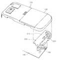
도 1은 본 발명의 일 실시예에 따른 전자장치인 이동통신 단말기의 케이스를 부분 절개하여 도시한 개략 사시도이며, 도 2는 본 발명에 따른 안테나 패턴 프레임의 제 1 실시예의 개략 사시도이며, 도 3은 도 2의 안테나 패턴 프레임의 배면 사시도이며, 도 4는 도 2 및 도 3의 A-A선의 단면도이다.1 is a schematic perspective view showing a partially cut case of a mobile communication terminal which is an electronic device according to an embodiment of the present invention, FIG. 2 is a schematic perspective view of a first embodiment of an antenna pattern frame according to the present invention, and FIG. 2 is a rear perspective view of the antenna pattern frame of FIG. 2, and FIG. 4 is a cross-sectional view taken along line AA of FIGS. 2 and 3.
도 1 내지 도 4를 참조하면, 본 발명의 일 실시예에 따른 안테나 패턴이 형 성되는 방사체(220)가 이동통신 단말기(100)의 케이스(120)에 매립되어 있는 것을 알 수 있다. 안테나 패턴이 형성되는 방사체(220)를 상기 케이스(120)의 내측에 형성시키기 위해 안테나 패턴이 형성되는 방사체(220)를 방사체 프레임(210) 상에 형성시킨 안테나 패턴 프레임(200)이 필요하다.1 to 4, it can be seen that the
본 발명의 일 실시예에 따른 전자장치의 케이스의 내측에 안테나 패턴을 형성하기 위한 안테나 패턴 프레임(200)은 안테나 패턴부(222)가 형성되는 방사체(220), 연결 단자부(224) 및 방사체 프레임(210)을 포함할 수 있다.An
상기 방사체(220)는 알루미늄이나 구리 등의 도전재로 이루어져 외부신호를 수신하여 이동통신 단말기(100)와 같은 전자장치의 신호처리장치로 전달할 수 있다. 또한, 상기 방사체(220)는 다양한 대역의 외부 신호를 수신하기 위해 미앤더 라인(Meander line)을 이루는 안테나 패턴부(222)를 가진다.The
상기 연결 단자부(224)는 수신된 외부신호를 전자장치에 전송하며, 방사체(220)의 일부를 절곡, 포밍(forming), 드로잉(drawing) 가공하여 형성할 수 있다. 또한, 상기 연결 단자부(224)는 방사체(220)와 별도로 제조된 후 상기 방사체(220)에 연결되어 제조될 수 있다(도 7 참조). The
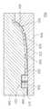
한편, 방사체 프레임(210)은 편평한 평면부(260)와 곡률을 가지는 커브부(240)로 이루어 지는 입체 구조일 수 있다. 상기 방사체(220)는 상기 방사체 프레임(210)의 커브부(240)에 배치되도록 플렉스블 한 특성을 가질 수 있다.On the other hand, the
상기 방사체 프레임(210)은 사출 구조물로, 상기 안테나 패턴부(222)는 방사 체 프레임(210)의 일면(210a)에 형성되며, 상기 연결 단자부(224)는 상기 일면(210a)의 반대면(210b)에 형성될 수 있다.The
전자장치 케이스(120)의 내부에 매립되는 방사체(220)의 구조는 외부신호를 수신하는 안테나 패턴부(222)와 외부신호를 전자장치에 전송하는 연결 단자부(224)가 다른 평면 상에 형성될 수 있다.In the structure of the
상기 방사체 프레임(210)은 상기 전자장치 케이스(120) 내부에 안테나 패턴부(222)가 형성된 일면(210a)을 접착하여 상기 전자장치 케이스(120) 내부에 안테나 패턴을 매립할 수 있다.The
또한, 안테나 패턴 프레임(200)을 금형에 넣고 인서트 사출함으로써 상기 전자장치 케이스(120) 내부에 안테나 패턴을 매립할 수 있다.In addition, the antenna pattern may be embedded in the
따라서, 안테나 패턴 프레임(200)은 안테나 패턴부(222)가 형성된 방사체(220)를 전자장치 케이스(120) 내부에 매립하기 위한 1차 사출물로서의 기능을 한다.Therefore, the
또한, 상기 방사체(220)는 상기 방사체 프레임(210)과 경계면이 서로 동일하게 이루어 질 수 있다. 이와 같은 구성은 1차 사출 이후, 안테나 패턴 프레임(200)을 금형에 넣고 2차 인서트 사출할 때, 레진과 같은 사출물의 흐름성을 증가시키는 효과가 있다.In addition, the
한편, 상기 방사체(220)에는 몰드 성형시 제조금형(300)의 가이드핀(328, 도 9 참조)이 위치되어 상기 방사체 프레임(210) 상에서 상기 방사체(220)의 움직임을 방지하는 가이드핀 홀(225)이 형성될 수 있다.Meanwhile, a guide pin hole 328 (see FIG. 9) of the
또한, 상기 방사체(220)에는 몰드 성형시 제조금형(300)의 접촉핀(326, 도 9 참조)이 위치되어 상기 방사체 프레임(210) 상에서 상기 방사체(220)의 움직임을 방지하는 접촉핀 홀(223)이 형성될 수 있다.In addition, a contact pin hole 326 (see FIG. 9) of the
상기 접촉핀(326)과 가이드핀(328)은 방사체(220) 상에 형성될 수 있으며, 몰드 성형 후 접촉핀(326) 아래의 방사체 프레임(210)은 충진되어 있으나, 가이드핀(328) 아래의 방사체 프레임(210)은 홀이 형성되어 있다.The contact pins 326 and the guide pins 328 may be formed on the
상기 방사체(220) 상에 형성되는 접촉핀 홀(223)에 끼워지는 접촉핀(326)은 1차 사출시 제조금형(300) 내에서 방사체(220)의 수평방향 이동을 방지하는 기능을 한다. 또한, 상기 방사체(220) 상에 형성되는 가이드핀 홀(225)에 끼워지는 가이드핀(225)는 1차 사출시 제조금형(300) 내에서 방사체(220)의 수직방향 이동을 방지하는 기능을 한다.The contact pins 326 fitted into the contact pin holes 223 formed on the
이와 같이 구성되는 안테나 패턴 프레임(200)의 다양한 실시예에 대해서 상세히 설명한다.Various embodiments of the
[안테나 패턴 프레임의 제1실시예][First Embodiment of Antenna Pattern Frame]
도 2 내지 도 4는 안테나 패턴 프레임의 제1실시예를 나타내는 도면이다.2 to 4 are diagrams illustrating a first embodiment of an antenna pattern frame.
제1실시예에 따른 안테나 패턴 프레임(200)의 방사체(220)는 상기 연결 단자부(224)와 상기 안테나 패턴부(222)와 각각 절곡되어 연결되는 절곡 연결부(226)를 구비할 수 있다.The
상기 절곡 연결부(226)는 안테나 패턴부(222)와 연결 단자부(224)를 다른 평면 상에 구성할 수 있으며, 전자장치의 케이스에 매립되지 않는 연결 단자부(224)는 안테나 패턴 프레임(200)의 반대면(210b)에서 노출될 수 있다.The
즉, 상기 절곡 연결부(226)를 기준으로 안테나 패턴부(222)와 연결 단자부(224)가 절곡되어, 방사체(220)가 3차원 곡면의 형상으로 구현될 수 있다.That is, the
3차원 곡면 형상의 방사체(220)를 지지하기 위해 상기 방사체 프레임(210)의 반대면(210b)에는 방사체 지지부(250)가 돌출될 수 있다.In order to support the
상기 방사체 지지부(226)는 상기 반대면(210b)으로 노출되는 연결 단자부(224)와 절곡 연결부(226)를 견고히 지지할 수 있다.The
[안테나 패턴 프레임의 제2실시예][Second embodiment of antenna pattern frame]
도 5는 본 발명에 따른 안테나 패턴 프레임의 제2실시예의 개략 단면도이다.5 is a schematic cross-sectional view of a second embodiment of an antenna pattern frame according to the present invention.
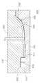
도 5를 참조하면, 본 발명에 따른 안테나 패턴 프레임의 제2실시예는 도 2 내지 도 4의 제1실시예와 유사하게 안테나 패턴 프레임(200)의 방사체(220)는 상기 연결 단자부(224)와 상기 안테나 패턴부(222)와 각각 절곡되어 연결되는 절곡 연결부(226)를 구비할 수 있다.Referring to FIG. 5, the second embodiment of the antenna pattern frame according to the present invention is similar to the first embodiment of FIGS. 2 to 4, and the
다만, 제2실시예의 상기 절곡 연결부(226)는 상기 방사체 프레임(210)의 반대면에서 돌출되는 방사체 지지부(250)를 관통하는 구조로 이루어질 수 있다.However, the
[안테나 패턴 프레임의 제3실시예][Third Embodiment of Antenna Pattern Frame]
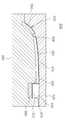
도 6은 안테나 패턴 프레임의 제3실시예를 나타내는 도면이다.6 shows a third embodiment of an antenna pattern frame.
도 6을 참조하면, 제1실시예 및 제2실시예와 유사하게, 안테나 패턴 프레임(200)의 방사체(220)가 상기 연결 단자부(224)와 안테나 패턴부(222)와 각각 절곡되어 연결되는 절곡 연결부(226)를 구비할 수 있다.Referring to FIG. 6, similar to the first and second embodiments, the
제3실시예의 방사체 프레임(210)은 안테나 패턴 프레임(200)의 반대면(210a)에서 돌출되는 구조의 방사체 지지부(250)를 가지지 못한다. 다만, 방사체 지지부(250)는 상기 방사체 프레임(210)과 동일 높이와 두께를 가져서 상기 방사체 프레임(210)과 경계 구분이 없다. 또한, 제3실시예의 상기 절곡 연결부(226)는 상기 방사체 프레임(210) 또는 방사체 지지부(250)를 관통하는 구조로 이루어질 수 있다.The
[안테나 패턴 프레임의 제4실시예][Fourth Embodiment of Antenna Pattern Frame]
도 7은 안테나 패턴 프레임의 제4실시예를 나타내는 도면이다.7 shows a fourth embodiment of an antenna pattern frame.
도 7을 참조하면, 제4실시예의 안테나 패턴 프레임(200)의 연결 단자부는 상기 안테나 패턴부(222)와 분리되어 있는 연결단자(270)로 이루어 질 수 있다.Referring to FIG. 7, the connection terminal portion of the
상기 연결단자(270)는 안테나 패턴부(222)와 상기 회로기판(140)을 연결하는 탄성체일 수 있다.The
특히, 연결단자(270)는 안테나 패턴부(222)와 회로기판(140)이 전기적 접속을 가능하게 하는 C-클립이나 포고 핀(pogo-pin) 등일 수 있으며, 상기 방사체 프레임(210)에 구멍을 형성하여 연결단자(270)를 끼울 수 있다.In particular, the
이하에서는 이와 같이 다양한 실시예로 제조되는 안테나 패턴 프레임(200)의 제조하는 방법과 제조금형에 대하여 상세히 살펴보기로 한다.Hereinafter, a method and a manufacturing mold of the
도 8은 본 발명에 따른 안테나 패턴 프레임의 제조에 사용되는 방사체의 개략 사시도이며, 도 9는 본 발명에 따른 안테나 패턴 프레임의 제조 방법을 설명하기 위한 안테나 패턴 프레임의 제조금형의 제1실시예의 모습을 도시한 개략 단면도이다. 도 10은 도 9의 제조금형에 수지재가 충진되는 모습을 도시한 개략도이다.8 is a schematic perspective view of a radiator used for manufacturing an antenna pattern frame according to the present invention, and FIG. 9 is a view of a first embodiment of a manufacturing mold of an antenna pattern frame for explaining a method of manufacturing an antenna pattern frame according to the present invention. It is a schematic sectional drawing. FIG. 10 is a schematic view showing a state in which a resin material is filled in the manufacturing mold of FIG. 9.
이하에서는 도 8 내지 도 10을 참조하여 본 발명의 일 실시예에 따른 안테나 패턴 프레임(200)의 제조방법을 단계별로 설명한다.Hereinafter, a method of manufacturing the
우선, 도 8에 도시된 바와 같이, 외부 신호를 수신하는 안테나 패턴부(222)와 상기 외부 신호를 전자장치에 전송하도록 상기 전자장치의 회로기판과 컨택되는 연결 단자부(224)가 다른 평면에 배치되는 방사체(220)를 제공한다.First, as shown in FIG. 8, the
이와 같은 방사체(220)에는 가이드핀 홀(225)이나 접촉핀 홀(223)들이 동시에 형성될 수 있다.In the
또한, 상기 방사체(220)는 안테나 패턴부(222)와 연결 단자부(226)을 각각 절곡하여 3차원 구조로 이루어질 수 있으며, 상기 안테나 패턴부(222)와 연결 단자부(226)는 절곡 연결부(226)에 의해 절곡 연결될 수 있다.In addition, the
이와 같은 방사체(220)를 제공한 후, 상기 방사체(220)를 제조금형(300)의 내부공간(350)에 배치한다. After providing the
상기 내부공간(350)은 상부금형(320) 및 하부금형(340)이 합형된 경우 형성되는 것으로, 상기 상부금형(320) 또는 하부금형(340)에 형성된 홈이 상부금형(320) 및 하부금형(340)의 합형으로 내부공간(350)이 된다.The
상기 상부금형(320) 및 하부금형(340)이 합형되면, 상기 안테나 패턴부(222)에 형성된 가이드핀 홀(225), 접촉핀 홀(223) 또는 가이드핀 홀(225) 및 접촉핀 홀(223)에 상기 상부 또는 하부 금형(320, 340)에 형성되는 가이드핀(328), 접촉핀(326) 또는 가이드핀(328) 및 접촉핀(326)이 통과 또는 접촉하여 상기 내부공간(350)에 방사체(220)가 고정될 수 있다.When the
상기 내부공간(250)은 안테나 패턴부(222)가 상기 전자장치의 케이스(120) 내부에 매립되도록 하는 방사체 프레임(210)이 되도록 수지재가 충진된다.The
이때, 상기 상부 또는 하부 금형(320, 340)의 내부공간(350)은 커브부가 형성되어 방사체 프레임(210)이 커브부(240)를 가지게 할 수 있다.In this case, the
또한, 상기 수지재는 상기 방사체(220)가 상기 방사체 프레임(210)과 경계면이 동일하게 충진되어, 상기 방사체 프레임(210)을 안테나 패턴이 매립되는 전자장치 케이스(120) 제조를 위해 금형에 넣고 사출할 때 수지재의 흐름을 좋게할 수 있다.In addition, the resin material is injected into the mold for manufacturing the
[안테나 패턴 프레임 제조금형의 제1실시예][First Embodiment of Antenna Pattern Frame Manufacturing Mold]
도 9 및 도 10을 참조하면, 본 발명에 따른 안테나 패턴 프레임(200)의 제조금형(300)을 상세히 알 수 있다.9 and 10, the
본 발명에 따른 안테나 패턴부(222)가 전자장치의 케이스(120) 내부에 매립되도록 하는 안테나 패턴 프레임(220)은 상부 및 하부 금형(320, 340) 및 수지재 주입부(370)를 포함할 수 있다.The
상기 상부 및 하부 금형(320, 340)에는 외부 신호가 수신되는 안테나 패턴부(222)와 전자장치의 회로 기판(140)에 컨택되는 연결 단자부(224)가 다른 평면에 배치되는 방사체(220)가 수용될 수 있다.In the upper and
상기 수지재 주입부(370)는 수지재가 유입되도록 하는 이동통로이며, 상기 상부, 하부 또는 상부 및 하부 금형(320) 어디라도 형성될 수 있다. 또한, 상기 상부 및 하부 금형(320, 340)이 합형된 경우, 상기 금형의 내부 공간(350)이 상기 안테나 패턴부(222)가 상기 전자장치의 케이스(120) 내부에 매립되도록 하는 방사체 프레임(210)이 되도록 상기 내부공간(350)으로 수지재가 유입되도록 한다.The resin
상기 상부, 하부 또는 상부 및 하부 금형(320, 340) 중 어느 하나에는 상기 방사체(220)에 형성된 가이드핀 홀(225), 접촉핀 홀(223) 또는 가이드핀 홀(225) 및 접촉핀 홀(223)을 관통 또는 접촉하도록 가이드핀(328), 접촉핀(326) 또는 가이드핀(328) 및 접촉핀(326)이 구비될 수 있다.Any one of the upper, lower or upper and
상기 상부 및 하부 금형(320, 340)의 내부 공간(350)은 상기 방사체 프레임(210)이 커브부(240)를 구비하도록 대응되는 형상의 공간을 구비할 수 있다.The
또한, 상기 상부 및 하부 금형(320, 340)의 내부 공간(350)은 연결 단자부(224)를 수용하며, 상기 연결 단자부(224)를 지지하는 방사체 지지부(250)가 형성되도록 하는 방사체 지지부 형성홈(346)을 구비할 수 있다.In addition, the
또한, 상기 상부, 하부 또는 상부 및 하부 금형(320, 340)에는 상기 방사체 지지부 형성홈(346)에 배치되는 연결 단자부(224)를 압착하여 상기 연결 단자부(224)를 상기 방사체 지지부 형성홈(346)에 밀착할 수 있도록 하는 압착핀(324)이 구비될 수 있다.In addition, the upper, lower or upper and
상기 압착핀(324)은 수지재 유입시 상기 연결 단자부(224) 아래로 수지재가 유입되는 것을 방지할 수 있다. 연결 단자부(224)의 일부 부분에 사출물이 덮여지게 되는 경우 전기적인 접속이 불안정하게 될 수 있는데, 상기 압착핀(324)은 이를 방지할 수 있다.The
[안테나 패턴 프레임 제조금형의 제2실시예][Second embodiment of antenna pattern frame manufacturing mold]
도 11은 본 발명에 따른 안테나 패턴 프레임의 제조 방법을 설명하기 위한 안테나 패턴 프레임의 제조금형의 제2실시예의 모습을 도시한 개략 단면도이며, 도 12는 도 11의 제조금형에 수지재가 충진되는 모습을 도시한 개략도이다.FIG. 11 is a schematic cross-sectional view showing a second embodiment of a manufacturing mold of an antenna pattern frame for explaining a method of manufacturing an antenna pattern frame according to the present invention, and FIG. 12 is a view in which a resin material is filled in the manufacturing mold of FIG. It is a schematic diagram showing.
도 11 및 도 12를 참조하면, 안테나 패턴 프레임 제조금형(300)의 제2실시예는 안테나 패턴 프레임 제조금형의 제1실시예와 이하에서 설명하는 점이외는 실질적으로 동일하다.11 and 12, the second embodiment of the antenna pattern
제2실시예는 상기 방사체의 움직임을 방지하는 가이드핀 또는 접촉핀 중 적어도 하나는 수지재의 유입으로 상기 금형(300) 내로 유입될 수 있다.In the second embodiment, at least one of the guide pin or the contact pin for preventing the movement of the radiator may be introduced into the
이와 같은 가이드핀 또는 접촉핀을 유동핀(345)으로 정의할 수 있다. 이와 같은 유동핀(345)은 수지재 유입 전에 방사체(220)를 제조금형(300)의 내부공 간(350)에서 지지하고 있으며, 사출액이 차오르는 시점에서 내부공간(350)에서 제조금형(300)으로 이동할 수 있다.Such a guide pin or a contact pin may be defined as the floating
상기 유동핀(345)을 사용함으로써, 제조금형(300)에 고정된 핀들과는 달리 핀 자국을 최소화할 수 있다.By using the
[안테나 패턴 프레임 제조금형의 제3실시예][Third Embodiment of Antenna Pattern Frame Manufacturing Mold]
도 13은 본 발명에 따른 안테나 패턴 프레임의 제조 방법을 설명하기 위한 안테나 패턴 프레임의 제조금형의 제3실시예의 모습을 도시한 개략 단면도이며, 도 14는 도 13의 제조금형에 수지재가 충진되는 모습을 도시한 개략도이다.FIG. 13 is a schematic cross-sectional view showing a third embodiment of a manufacturing mold of an antenna pattern frame for explaining a method of manufacturing an antenna pattern frame according to the present invention, and FIG. 14 is a view in which a resin material is filled in the manufacturing mold of FIG. It is a schematic diagram showing.
도 13 및 도 14를 참조하면, 안테나 패턴 프레임 제조금형(300)의 제3실시예는 제2실시예와 마찬가지로 안테나 패턴 프레임 제조금형의 제1실시예와 이하에서 설명하는 점이외에는 실질적으로 동일하다.13 and 14, the third embodiment of the antenna pattern
제3실시예는 상기 방사체 지지부 형성홈(346)에서 상기 연결 단자부(224)가 안착되는 부분은 마그넷(380)이 형성될 수 있다.In a third embodiment, a
상기 마그넷(380)은 제1실시예의 압착핀(324)와 유사하게, 상기 연결 단자부(224) 아래부분으로 수지재가 유입되는 것을 방지할 수 있으며, 상기 연결 단자부(244)의 일부에 사출물이 덮여져서 전기적인 접속이 불안정하게 되는 것을 방지할 수 있다.The
[방사체의 들뜸 현상 방지한 안테나 패턴 프레임 및 그 제조방법][Antenna Pattern Frame Preventing Lifting of Radiator and Its Manufacturing Method]
이하에서는, 안테나 패턴이 견고하게 고정되는 방사체 프레임을 구비하는 안테나 프레임과, 상기 방사체 프레임에 안테나 패턴부를 견고하게 고정하여 들뜸현상을 없앨 수 있는 안테나 프레임의 제조방법을 설명한다.Hereinafter, an antenna frame including a radiator frame to which the antenna pattern is firmly fixed, and a method of manufacturing an antenna frame capable of firmly fixing the antenna pattern portion to the radiator frame and eliminating the lifting phenomenon will be described.
도 15의 (a) 내지 (d)는 본 발명의 일 실시예에 따른 안테나 패턴이 형성되는 방사체를 안테나 패턴 프레임에 고정하는 방법에 사용되는 안테나 방사체의 형상을 도시한 개략 사시도이다.15A to 15D are schematic perspective views illustrating the shape of an antenna radiator used in a method of fixing a radiator on which an antenna pattern is formed to an antenna pattern frame according to an embodiment of the present invention.
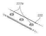
도 15의 (a) 내지 (d)는 접촉면 확장부(227)가 형성되는 방사체(220)를 안테나 패턴 프레임(200)에 고정하기 위한 방사체의 다양한 실시예를 설명한다.15A to 15D illustrate various embodiments of the radiator for fixing the
도 15의 (a) 내지 (d)의 방사체(220)가 적용되는 안테나 패턴 프레임(200)은 도 15의 (a)에 도시된 접촉면 확장부(227)가 형성되는 방사체(220)를 도 2 내지 도 7에서 설명되는 안테나 패턴 프레임(200)의 방사체(220)와 대체하여 설명할 수 있다.The
즉, 도 15의 (a) 내지 (d)의 실시예에 따른 안테나 패턴 프레임(200)은 방사체(220), 방사체 프레임(210) 및 접촉면 확장부(227)를 포함할 수 있다.That is, the
상기 방사체(220)와 방사체 프레임(210)은 도 2 내지 도 4에서 설명한 것을 그대로 원용할 수 있다.The
다만, 접촉면 확장부(227)가 형성되는 방사체(220)는 상기 방사체 프레임(210)의 몰드 사출 성형 시, 상기 방사체(220)의 상기 방사체 프레임(210) 상에서 들뜸 현상을 방지하는 역할을 한다.However, the
이는 몰드 성형을 위해 상기 방사체(220)를 금형에 넣고 수지재를 충진시키 면, 상기 접촉면 확장부(227)가 상기 수지재와의 접촉면적을 넓힐 수 있으므로 상기 방사체(220)를 사출물 내에서 견고히 고정시킬 수 있다.This is because when the
상기 접촉면 확장부(227)는 도 15의 (a)와 같이 상기 방사체(220)의 측면에지에서 연장되고 절곡되어 상기 방사체 프레임(210)에 삽입되는 블레이드(227a)일 수 있다.The contact surface extension 227 may be a
또한, 상기 접촉면 확장부(227)는 도 15의 (b)와 같이 상기 방사체(220)에서 홀(227b)을 형성하여 사출물이 들어가게 함으로써 접촉면을 확장하고, 위치를 정확하게 고정시킬 수 있다.In addition, the contact surface expansion unit 227 may form a
또한, 상기 접촉면 확장부(227)는 도 15의 (c)와 같이 상기 방사체(220)에서 엠보를 형성하여 방사체(220)를 사출물과 접촉면적을 확장하고, 위치를 정확히 알려낼 수 있다.In addition, the contact surface extension 227 may form an emboss in the
또한, 상기 접촉면 확장부(227)는 도 15의 (d)와 같이 상기 방사체(220)의 안테나 패턴부(222)의 일부를 비스듬하게 접혀져, 상기 방사체 프레임(210)에 삽입되어 형성될 수 있다.In addition, the contact surface extension part 227 may be formed by being folded obliquely to a part of the
방사체(220)의 들뜸 현상을 방지하기 위한 본 실시예의 안테나 패턴 프레임(200)은 도 2 내지 도 7의 안테나 패턴 프레임 모두에 적용될 수 있다.The
상기 방사체 프레임(210)에 안테나 패턴부를 견고하게 고정하여 들뜸현상을 없앨 수 있는 안테나 프레임의 제조방법은 몰드 사출시 몰드 수지재와 접촉면적을 확장하는 접촉면 확장부(227)가 형성되는 방사체(220)를 금형(300)에 넣는 점 외에는 도 8 내지 도 14에서 설명한 사출 방법 모두를 그대로 원용할 수 있다.In the method of manufacturing an antenna frame capable of firmly fixing the antenna pattern part to the
[안테나 패턴 방사체가 매립된 전자장치 케이스, 이의 제조방법 및 제조방법, 이동통신 단말기][Electronic device case in which antenna pattern radiator is embedded, manufacturing method and manufacturing method thereof, mobile communication terminal]
도 16은 본 발명의 일 실시예에 따른 안테나 패턴 방사체가 매립된 전자장치인 이동통신 단말기의 케이스의 분해 사시도이다.16 is an exploded perspective view of a case of a mobile communication terminal which is an electronic device with an antenna pattern radiator embedded therein according to an embodiment of the present invention.
도 16을 참조하면, 본 발명의 일 실시예에 따른 안테나 패턴 방사체(220)가 매립된 전자장치의 케이스(120)는 방사체(220), 방사체 프레임(210) 및 케이스 프레임(210)을 포함한다.Referring to FIG. 16, a
상기 방사체(220)와 상기 방사체 프레임(210)은 도 2 내지 도 7의 실시예에서 설명한 것으로 대체한다.The
상기 케이스 프레임(130)은 안테나 패턴부(222)가 형성된 상기 방사체 프레임(210)의 일면을 덮어, 상기 안테나 패턴부(222)가 상기 방사체 프레임(210)과 사이에서 매립되도록 한다.The
상기 방사체 프레임(210)과 상기 케이스 프레임(130)은 경계의 구분이 없이 일체화 된다. 상기 전자장치의 케이스(120)를 배면에서 보면, 안테나 패턴부(222)는 보이지 않고 연결 단자부(224)만 보일 수 있다.The
상기 방사체 프레임(210), 케이스 프레임(130), 또는 방사체 프레임(210) 및 케이스 프레임(130)은 사출 몰드 성형되어 형성될 수 있다. 특히, 방사체 프레임(210)과 케이스 프레임(130)이 별개의 사출 기구물로 이루어지는 경우는 방사체(220)가 형성되는 방사체 프레임(210)을 상기 케이스 프레임(130)에 접착하여 제조한다.The
한편, 상기 케이스 프레임(130)이 상기 방사체 프레임(210)에 사출 몰드 성형되어 2중 사출몰딩될 수 있다. 즉, 상기 방사체 프레임(210)을 금형에 넣고, 인서트 사출함으로써, 상기 방사체 프레임(210)과 케이스 프레임(130)을 일체화 시킬 수 있다.Meanwhile, the
상기 방사체 프레임(210)에 형성되는 가이드핀 홀(225)이나 접촉핀 홀(223)은 전자장치 케이스의 제조금형(500)에 넣는 경우 상기 제조금형(500)에서 형성되는 가이드핀이나 접촉핀(미도시)과 결합하여 안테나 패턴 프레임(200)이 상기 제조금형(500)에서 움직이는 것을 방지할 수 있다.When the
이하에서는 도 16 내지 도 19를 참조하여 전자장치 케이스의 제조방법 및 제조금형을 상세히 살펴본다.Hereinafter, a manufacturing method and a manufacturing mold of an electronic device case will be described in detail with reference to FIGS. 16 to 19.
본 발명에 따른 전자장치 케이스의 제조방법은 우선, 외부 신호를 수신하는 안테나 패턴부(222)와 전자장치의 회로기판(140)의 연결단자(144)에 컨택되는 연결 단자부(224)가 다른 평면에 배치되는 방사체(220)를 제공한다.In the method of manufacturing an electronic device case according to the present invention, first, the
그리고, 상기 방사체(220)를 방사체 프레임(210) 제조를 위한 상부 또는 하부 금형(300)의 내부공간(350)에 배치하고 수지재를 유입시켜 방사체(220)가 일면 에 형성되는 방사체 프레임(210)을 제조한다.The
또한, 상기 방사체(220)가 상기 방사체 프레임(210)과의 사이에서 매립되도록 상기 방사체 프레임(210)을 케이스 프레임(130)과 일체화 하여 안테나가 매립되는 전자장치 케이스(120)를 제조한다.In addition, the
도 17은 본 발명의 일 실시예에 따른 안테나 패턴 방사체가 매립된 전자장치의 케이스의 제조방법의 제 1 실시예를 도시한 개략도이다.17 is a schematic diagram illustrating a first embodiment of a method of manufacturing a case of an electronic device having an antenna pattern radiator embedded therein according to an embodiment of the present disclosure.
도 17을 참조하면, 상기 케이스 프레임(130)은 상기 방사체 프레임(210)과 대응되는 형상의 방사체 수용홈(122)을 가지는 별도의 사출물이며, 상기 방사체 수용홈(122)에 상기 방사체 프레임(210)을 접착시켜서 안테나 패턴 방사체가 매립된 전자장치의 케이스(120)를 제조할 수 있다.Referring to FIG. 17, the
상기 안테나 패턴 프레임(200)의 방사체(220) 표면에는 접착제 층(410)이 형성되어 있다.An
도 18은 본 발명의 일 실시예에 따른 안테나 패턴 방사체가 매립된 전자장치의 케이스의 제조방법의 제2실시예에 사용되는 전자장치의 케이스 제조금형의 개략도이며, 도 19는 도 18의 제조금형에 수지재가 충진되는 모습을 도시한 개략도이다.FIG. 18 is a schematic diagram of a case manufacturing mold of an electronic device used in a second embodiment of a method of manufacturing a case of an electronic device having an antenna pattern radiator embedded therein, and FIG. 19 is a manufacturing mold of FIG. 18. Is a schematic diagram showing how the resin material is filled.
도 18 및 도 19를 참조하면, 안테나 패턴 방사체(220)가 매립된 전자장치의 케이스(120)의 제조는 상기 방사체 프레임(210)을 수용하는 내부공간(550)이 형성 되는 전자장치 케이스 제조금형(500)에 배치하고 수지재를 유입시켜서 방사체 프레임(210)을 전자장치 케이스(120)로 일체화한다.18 and 19, in manufacturing the
한편, 상기 방사체 프레임(210)과 상기 케이스 프레임(120)은 경계의 구분이 없도록 형성될 수 있다.On the other hand, the
안테나 패턴 프레임(200) 사출을 1차 사출, 전자장치 케이스(120) 사출을 2차 사출이라고 할 때, 2차 사출 또한 1차 사출과 같이 안테나 패턴 프레임(200)이 2차 사출 제조금형(500)에서 움직이지 않도록 할 수 있다.When the injection of the
또한, 제조금형(500)의 내부공간(550)은 전자장치 케이스(120)가 커브부를 가지도록 하는 커브 형성부(524)를 구비할 수 있다.In addition, the
한편, 2차 사출로 안테나 패턴이 매립되는 전자장치 케이스(120)를 제조하기 위한 전자장치 케이스 제조금형은 외부 신호를 수신하는 안테나 패턴부(222)와 전자장치의 회로기판에 컨택되는 연결 단자부(224)를 다른 평면에 형성되는 방사체(220)가 구비되는 방사체 프레임(210)이 수용되는 전자장치 케이스 제조 상부 또는 하부 금형(520, 540) 및 상기 상부, 하부 또는 상기 상부 및 또는 하부 금형(520, 540)에 형성되어, 상기 상부 또는 하부 금형(520, 540)이 합형된 경우 상기 금형 내에 형성되는 내부공간(550)이 전자장치 케이스(120)가 되도록 상기 내부공간으로 수지재가 유입되도록 하는 수지재 주입부(570)를 포함할 수 있다.Meanwhile, the electronic device case manufacturing mold for manufacturing the
방사체 프레임(210) 또한, 방사체(220)와 마찬가지로, 가이드핀 홀이나 접촉 핀 홀이 형성되며, 상기 가이드핀 홀이나 접촉핀 홀이 제조금형(500)에 형성되는 가이드핀이나 접촉핀에 고정될 수 있다. 이는 제조금형(500)에서 상기 방사체 프레임(210)이 이동하지 않도록 하기 위함이다.Like the
이와 같이 제조된 안테나 패턴이 매립된 전자장치 케이스는 이동통신 단말기(100)에 응용될 수 있다.The electronic device case having the antenna pattern manufactured as described above may be applied to the
즉, 본 발명에 따른 안테나 패턴이 매립된 전자장치인 이동통신 단말기(100)는 방사체 프레임(210), 케이스 프레임(130) 및 회로기판(140)을 포함할 수 있다.That is, the
상기 방사체 프레임(210)과 케이스 프레임(130)은 지금까지 설명한 모든 실시예가 다 적용될 수 있으며, 그 제조방법 또한 그러하다.The
따라서, 이동통신 단말기(100)의 구체적인 설명은 상기 상술한 설명으로 대체하도록 한다.Therefore, the detailed description of the
[그라운드 접지부가 형성되는 안테나 패턴 프레임이 적용되는 전자장치][Electronic device to which antenna pattern frame with ground ground is formed]
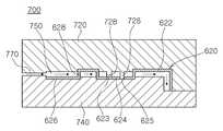
도 20은 본 발명의 다른 일 실시예에 따른 그라운드 접지부가 형성되는 안테나 패턴 프레임의 개략 사시도이며, 도 21은 본 발명의 다른 일 실시예에 따른 그라운드 접지부가 형성되는 안테나 패턴 방사체의 개략 사시도이다.20 is a schematic perspective view of an antenna pattern frame having a ground ground portion according to another embodiment of the present invention, and FIG. 21 is a schematic perspective view of an antenna pattern radiator having a ground ground portion according to another embodiment of the present invention.
본 발명의 다른 일 실시예에 따른 그라운드 접지부가 형성되는 안테나 패턴 프레임(600)은 안테나 패턴을 케이스에 매립할 수 있는 전자장치 중 노이즈 부분의 개선이 필요한 노트북 등에 주로 이용될 수 있다.The
본 발명의 다른 일 실시예에 따른 그라운드 접지부가 형성되는 안테나 패턴 프레임(600)은 방사체(620), 그라운드 접지부(626) 및 방사체 프레임(610)을 포함할 수 있다.An
본 실시예의 안테나 패턴 프레임(600)이 도 2 내지 도 7의 안테나 패턴 프레임(200)과 다른점은 방사체(620)에서 그라운드 접지부(626)가 연장되어 형성된다는 점이며, 그라운드 접지부(626)를 구성하기 위해 방사체 프레임(610)의 형상이 변형될 수 있다.The
상기 그라운드 접지부(626)는 상기 방사체 프레임(610)에서 단차져서 형성되는 그라운드 접지부 지지부(612)로 지지될 수 있다.The
상기 방사체 프레임(610)의 일면(610a)에는 상기 안테나 패턴부(622)가 형성될 수 있으며, 상기 방사체 프레임(610)의 일면(610a)의 반대면(610b)에 형성될 수 있다.The
이와 같은 방사체 프레임(610)은 상기 안테나 패턴부(622)가 전자장치의 케이스 내에 매립되어 구성될 수 있다.The
상기 안테나 패턴 프레임(600)의 상기 방사체(620) 또한, 도 2 내지 도 7의 안테나 패턴 프레임(200)과 마찬가지로, 상기 방사체 프레임(610)의 반대면(610b)에 형성되며 상기 외부신호를 회로 기판으로 전달하는 연결 단자부(624)를 구비할 수 있다.The
또한, 상기 방사체 프레임(610)에는 상기 방사체(620)와 그라운드 접지부(626)를 절곡 연결하는 절곡 연결부(628)가 관통될 수 있다. 상기 절곡 연결 부(628)가 상기 방사체 프레임(610)을 관통함으로써, 상기 방사체(620)가 상기 방사체 프레임(610) 상에서 견고히 고정될 수 있다.In addition, the
한편, 상기 방사체(620)에는 몰드 성형시 제조금형(700)의 접촉핀(728)이 위치되어 상기 제조금형(700) 상기 방사체(620)의 움직임을 방지하는 접촉핀 홀(623)이 형될 수 있다.Meanwhile, a
또한, 상기 방사체(620)에는 몰드 성형시 제조금형(700)의 가이드핀(726)이 위치되어 상기 제조금형(700) 내에서 상기 방사체(620)의 움직임을 방지하는 접촉핀 홀(625)이 형성될 수 있다.In addition, a
도 22는 본 발명의 다른 일 실시예에 따른 그라운드 접지부가 형성되는 안테나 패턴 프레임의 제조방법에 사용되는 안테나 패턴 프레임 제조금형의 개략 단면도이다.22 is a schematic cross-sectional view of an antenna pattern frame manufacturing mold used in the method of manufacturing an antenna pattern frame having a ground ground portion according to another embodiment of the present invention.
본 발명의 다른 일 실시예에 따른 그라운드 접지부가 형성되는 안테나 패턴 프레임의 제조방법은 우선, 외부 신호를 수신하는 안테나 패턴부(622)와 상기 안테나 패턴부(622)와 다른 평면에 배치되는 그라운드 접지부(626)가 형성되는 방사체(620)를 제공할 수 있다.According to another aspect of the present invention, there is provided a method of manufacturing an antenna pattern frame, in which a ground ground portion is formed. First, an
그리고, 상기 방사체(610)를 수용하는 내부공간(750)이 형성되는 제조금형(700)에 상기 방사체(620)를 배치할 수 있다.In addition, the
상기 제조금형(700)에 상기 방사체(620)를 배치한 후, 상기 내부공간(750)에 상기 제조금형(700)에 형성되는 수지재 주입부(770)를 통해 수지재를 충진하여 상 기 내부공간(750)이 상기 방사체(620)가 전자장치 케이스 내부에 매립되도록 하는 방사체 프레임(610)이 되도록 한다.After the
상기 방사체(610)를 상기 제조금형(700)에 배치할 때, 상기 방사체(620)에 형성된 가이드핀 홀(625), 접촉핀 홀(623) 또는 가이드핀 홀(625) 및 접촉핀 홀(623)에 상기 제조금형(700)에 형성되는 가이드핀(726), 접촉핀(728) 또는 가이드핀(726) 및 접촉핀(728)을 통과 또는 접촉시켜 고정할 수 있다.When the
상기 내부공간(750)에는 상기 연결 단자부(624)가 수용되는 홈이 형성될 수 있으며, 상기 수용홈에 상기 연결 단자부(624)를 배치하여 몰딩할 수 있다.A groove may be formed in the
본 발명의 다른 일 실시예에 따른 그라운드 접지부가 형성되는 안테나 패턴 프레임의 제조금형(700)은 외부 신호를 수신하는 안테나 패턴부(622)와 상기 안테나 패턴부(622)와 다른 평면에 배치되는 그라운드 접지부(626)가 형성되는 방사체(620)가 수용되는 상부 또는 하부 금형(720, 740) 및 상기 상부, 하부 또는 상기 상부 및 하부 금형(720, 740)에 형성되어, 상기 상부 또는 하부 금형(720, 740)이 합형된 경우 상기 금형 내에 형성되는 내부공간(750)이 상기 방사체(620)가 전자장치 케이스 내부에 매립되도록 하는 안테나 패턴 프레임(600)이 되도록 상기 내부공간(750)으로 수지재가 유입되도록 하는 수지재 주입부(770)를 포함할 수 있다.The
또한, 상기 상부 또는 하부 금형(720, 740)에는 상기 방사체 프레임(610)에 형성되는 가이드핀 홀(625), 접촉핀 홀(623) 또는 가이드핀 홀(625) 및 접촉핀 홀(623)을 관통 또는 접촉하는 가이드핀(726), 접촉핀(728) 또는 접촉핀(726) 및 가이드핀(728)이 구비될 수 있다.In addition, the upper or
상기 상부, 하부 또는 상부 또는 하부 금형(720, 740)에는 상기 연결 단자부(624)를 수용할 수 있다. The
도 23은 본 발명의 다른 일 실시에에 따른 그라운드 접지부가 형성되는 안테나 패턴 프레임이 적용되는 전자장치인 노트북의 개략 분해 사시도이다.FIG. 23 is a schematic exploded perspective view of a notebook, which is an electronic device to which an antenna pattern frame having a ground ground portion is formed according to another embodiment of the present invention.
상기와 같이 제조된 안테나 패턴부(622), 연결 단자부(624), 그라운드 접지부(626)가 형성되는 방사체 프레임(610)은 전자장치(800)인 노트북의 케이스에 안테나 패턴부(622)가 매립될 수 있다.The
즉, 본 발명에 따른 전자장치(800)는 방사체 프레임(610), 케이스(820) 및 회로기판(600)을 포함할 수 있다.That is, the
상기 방사체 프레임(610)은 지금까지 설명한 모든 실시예가 다 적용될 수 있으며, 그 제조방법 또한 그러하다.The
따라서, 전자장치(800)의 구체적인 설명은 상기 상술한 설명으로 대체하도록 한다.Therefore, the detailed description of the
본 발명의 일 실시예에 따른 안테나 패턴 프레임, 그 제조방법 및 제조금형에 의하면, 안테나 패턴부가 형성되는 방사체를 전자장치의 케이스에 매립할 수 있으므로, 종래의 외장형 타입 안테나가 가지는 외부충격에 대한 취약성 문제점 및 내장형 타입 안테나가 가지는 부피 증가의 문제점을 해결할 수 있다.According to the antenna pattern frame, the manufacturing method and the manufacturing mold according to an embodiment of the present invention, since the radiator formed with the antenna pattern portion can be embedded in the case of the electronic device, the vulnerability to the external impact of the conventional external type antenna It is possible to solve the problem of the volume increase of the built-in type antenna.
또한, 전자장치의 케이스에 플렉스블 재질의 안테나가 매립될 수 있으므로, 접착제 를 붙이는 것에 비해 안테나의 성능이 향상되며 내구성이 향상된다.In addition, since the antenna of the flexible material may be embedded in the case of the electronic device, the performance of the antenna is improved and durability is improved compared to attaching the adhesive.
또한, 안테나를 보호필름 없이 전자장치 케이스에 매립할 수 있으므로, 케이스 자체를 곡면과 같은 3차원 형상으로 제조할 수 있어 외관의 형상등을 다양화할 수 있다.In addition, since the antenna can be embedded in the electronic device case without a protective film, the case itself can be manufactured in a three-dimensional shape such as a curved surface to vary the shape of the appearance.
또한, 안테나 필름을 이용하지 않으므로, 제조공정이 용이해지며, 제조비용을 저감할 수 있는 효과가 있다.In addition, since the antenna film is not used, the manufacturing process is easy, and there is an effect that the manufacturing cost can be reduced.
또한, 방사체와 연결 단자부를 안테나 패턴 프레임에 견고히 지지할 수 있으므로 안테나 패턴부가 프레임 상에서 들뜸현상이 없어지며, 전자장치의 회로기판과 견고히 연결할 수 있는 효과가 있다.In addition, since the radiator and the connection terminal portion can be firmly supported on the antenna pattern frame, the antenna pattern portion is removed from the frame, and there is an effect that it can be firmly connected to the circuit board of the electronic device.
또한, 안테나가 필요한 모든 전자장치에 적용될 수 있으므로, 안테나 패턴 프레임을 다양하게 응용할 수 있는 효과가 있다.In addition, since the antenna can be applied to all the electronic devices that need, there is an effect that can be applied to a variety of antenna pattern frame.
도 1은 본 발명의 일 실시예에 따른 전자장치인 이동통신 단말기의 케이스를 부분 절개하여 도시한 개략 사시도.1 is a schematic perspective view showing a partially cut case of a mobile communication terminal which is an electronic device according to an embodiment of the present invention;
도 2는 본 발명에 따른 안테나 패턴 프레임의 제 1 실시예의 개략 사시도.2 is a schematic perspective view of a first embodiment of an antenna pattern frame according to the present invention;
도 3은 도 2의 안테나 패턴 프레임의 배면 사시도.3 is a rear perspective view of the antenna pattern frame of FIG. 2;
도 4는 도 2 및 도 3의 A-A선의 단면도.4 is a cross-sectional view taken along the line A-A of FIGS. 2 and 3;
도 5는 본 발명에 따른 안테나 패턴 프레임의 제 2 실시예의 개략 단면도.5 is a schematic cross-sectional view of a second embodiment of an antenna pattern frame according to the present invention;
도 6은 본 발명에 따른 안테나 패턴 프레임의 제 3 실시예의 개략 단면도.6 is a schematic sectional view of a third embodiment of an antenna pattern frame according to the present invention;
도 7은 본 발명에 따른 안테나 패턴 프레임의 제 4 실시예의 개략 단면도.7 is a schematic sectional view of a fourth embodiment of an antenna pattern frame according to the present invention;
도 8은 본 발명에 따른 안테나 패턴 프레임의 제조에 사용되는 방사체의 개략 사시도.8 is a schematic perspective view of a radiator used in the manufacture of an antenna pattern frame according to the present invention;
도 9는 본 발명에 따른 안테나 패턴 프레임의 제조 방법을 설명하기 위한 안테나 패턴 프레임의 제조금형의 제1실시예의 모습을 도시한 개략 단면도.9 is a schematic cross-sectional view showing a first embodiment of a manufacturing mold of an antenna pattern frame for explaining a method of manufacturing an antenna pattern frame according to the present invention.
도 10은 도 9의 제조금형에 수지재가 충진되는 모습을 도시한 개략도.10 is a schematic view showing a state in which a resin material is filled in the manufacturing mold of FIG.
도 11은 본 발명에 따른 안테나 패턴 프레임의 제조 방법을 설명하기 위한 안테나 패턴 프레임의 제조금형의 제2실시예의 모습을 도시한 개략 단면도.11 is a schematic cross-sectional view showing a second embodiment of a mold for manufacturing an antenna pattern frame for explaining a method for manufacturing an antenna pattern frame according to the present invention.
도 12는 도 11의 제조금형에 수지재가 충진되는 모습을 도시한 개략도.12 is a schematic view showing a state in which a resin material is filled in the manufacturing mold of FIG.
도 13은 본 발명에 따른 안테나 패턴 프레임의 제조 방법을 설명하기 위한 안테나 패턴 프레임의 제조금형의 제3실시예의 모습을 도시한 개략 단면도.Figure 13 is a schematic cross-sectional view showing a third embodiment of the manufacturing mold of the antenna pattern frame for explaining the manufacturing method of the antenna pattern frame according to the present invention.
도 14는 도 13의 제조금형에 수지재가 충진되는 모습을 도시한 개략도.14 is a schematic view showing a state in which a resin material is filled in the manufacturing mold of FIG.
도 15의 (a) 내지 (d)는 본 발명의 일 실시예에 따른 안테나 패턴이 형성되는 방사체를 안테나 패턴 프레임에 고정하는 방법에 사용되는 안테나 방사체의 형상을 도시한 개략 사시도.15A to 15D are schematic perspective views illustrating the shape of an antenna radiator used in a method of fixing a radiator on which an antenna pattern is formed to an antenna pattern frame according to an embodiment of the present invention.
도 16은 본 발명의 일 실시예에 따른 안테나 패턴 방사체가 매립된 전자장치인 이동통신 단말기의 케이스의 분해 사시도.16 is an exploded perspective view of a case of a mobile communication terminal which is an electronic device having an antenna pattern radiator embedded therein according to an embodiment of the present invention.
도 17은 본 발명의 일 실시예에 따른 안테나 패턴 방사체가 매립된 전자장치의 케이스의 제조방법의 제 1 실시예를 도시한 개략도.FIG. 17 is a schematic diagram illustrating a first embodiment of a method of manufacturing a case of an electronic device having an antenna pattern radiator embedded therein according to an embodiment of the present disclosure; FIG.
도 18은 본 발명의 일 실시예에 따른 안테나 패턴 방사체가 매립된 전자장치의 케이스의 제조방법의 제 2 실시예에 사용되는 전자장치의 케이스 제조금형의 개략도.18 is a schematic diagram of a case manufacturing mold of an electronic device used in a second embodiment of a method of manufacturing a case of an electronic device having an antenna pattern radiator embedded therein according to an embodiment of the present invention.
도 19는 도 18의 제조금형에 수지재가 충진되는 모습을 도시한 개략도.19 is a schematic view showing a state in which a resin material is filled in the manufacturing mold of FIG.
도 20은 본 발명의 다른 일 실시예에 따른 그라운드 접지부가 형성되는 안테나 패턴 프레임의 개략 사시도.20 is a schematic perspective view of an antenna pattern frame having a ground ground portion according to another embodiment of the present invention.
도 21은 본 발명의 다른 일 실시예에 따른 그라운드 접지부가 형성되는 안테나 패턴 방사체의 개략 사시도.21 is a schematic perspective view of an antenna pattern radiator having a ground ground portion according to another embodiment of the present invention.
도 22는 본 발명의 다른 일 실시예에 따른 그라운드 접지부가 형성되는 안테나 패턴 프레임의 제조방법에 사용되는 안테나 패턴 프레임 제조금형의 개략 단면도.22 is a schematic cross-sectional view of an antenna pattern frame manufacturing mold used in the method for manufacturing an antenna pattern frame having a ground ground portion according to another embodiment of the present invention.
도 23은 본 발명의 다른 일 실시에에 따른 그라운드 접지부가 형성되는 안테나 패턴 프레임이 적용되는 전자장치인 노트북의 개략 분해 사시도.FIG. 23 is a schematic exploded perspective view of a notebook, which is an electronic device to which an antenna pattern frame having a ground ground portion is formed according to another embodiment of the present invention; FIG.
<도면의 주요부분에 대한 부호의 설명><Description of the symbols for the main parts of the drawings>
100: 이동통신 단말기120: 케이스100: mobile communication terminal 120: case
200: 안테나 패턴 프레임220: 방사체200: antenna pattern frame 220: radiator
250: 접지 패턴 지지부300, 500, 700: 제조금형250:
626: 그라운드 접지부 800: 노트북626: ground ground 800: notebook
Claims (28)
Translated fromKoreanPriority Applications (8)
| Application Number | Priority Date | Filing Date | Title |
|---|---|---|---|
| KR1020090035635AKR100935954B1 (en) | 2009-04-23 | 2009-04-23 | Case of electronic device, method and mould for manufacturing the same, and mobile communication terminal |
| US12/608,818US8618989B2 (en) | 2009-04-23 | 2009-10-29 | Electronic device case, method and mold for manufacturing the same, and mobile communications terminal |
| JP2009251207AJP5130274B2 (en) | 2009-04-23 | 2009-10-30 | Electronic device case, manufacturing method and manufacturing mold thereof, mobile communication terminal |
| CN200910208368ACN101872888A (en) | 2009-04-23 | 2009-11-12 | Electronic device shell, manufacturing method and mould thereof and mobile communication terminal |
| CN201510347802.4ACN104953237A (en) | 2009-04-23 | 2009-11-12 | Electronic device case, method for manufacturing the same, and mobile communications terminal |
| DE102009046936.2ADE102009046936B4 (en) | 2009-04-23 | 2009-11-20 | Housing for an electronic device, method and form for making the same and mobile device |
| US13/973,103US9096029B2 (en) | 2009-04-23 | 2013-08-22 | Electronic device case, method and mold for manufacturing the same, and mobile communications terminal |
| US13/973,936US8922439B2 (en) | 2009-04-23 | 2013-08-22 | Electronic device case, method and mold for manufacturing the same, and mobile communications terminal |
Applications Claiming Priority (1)
| Application Number | Priority Date | Filing Date | Title |
|---|---|---|---|
| KR1020090035635AKR100935954B1 (en) | 2009-04-23 | 2009-04-23 | Case of electronic device, method and mould for manufacturing the same, and mobile communication terminal |
Related Child Applications (1)
| Application Number | Title | Priority Date | Filing Date |
|---|---|---|---|
| KR1020090096966ADivisionKR20100117009A (en) | 2009-10-12 | 2009-10-12 | Case of electronic device, method and mould for manufacturing the same, and mobile communication terminal |
Publications (1)
| Publication Number | Publication Date |
|---|---|
| KR100935954B1true KR100935954B1 (en) | 2010-01-12 |
Family
ID=41809579
Family Applications (1)
| Application Number | Title | Priority Date | Filing Date |
|---|---|---|---|
| KR1020090035635AExpired - Fee RelatedKR100935954B1 (en) | 2009-04-23 | 2009-04-23 | Case of electronic device, method and mould for manufacturing the same, and mobile communication terminal |
Country Status (5)
| Country | Link |
|---|---|
| US (3) | US8618989B2 (en) |
| JP (1) | JP5130274B2 (en) |
| KR (1) | KR100935954B1 (en) |
| CN (2) | CN104953237A (en) |
| DE (1) | DE102009046936B4 (en) |
Cited By (20)
| Publication number | Priority date | Publication date | Assignee | Title |
|---|---|---|---|---|
| KR101050160B1 (en) | 2010-06-25 | 2011-07-19 | 에이큐 주식회사 | Cell phone case with antenna and its manufacturing method |
| CN102195121A (en)* | 2010-03-15 | 2011-09-21 | 三星电机株式会社 | Electronic device case, mold for manufacturing the same, and mobile communications terminal |
| US20110260932A1 (en)* | 2010-04-22 | 2011-10-27 | Samsung Electro-Mechanics Co., Ltd. | Antenna pattern frame, electronic device case provided with antenna pattern frame and electronic device including electronic device case |
| CN102300437A (en)* | 2010-06-28 | 2011-12-28 | 三星电机株式会社 | Case of electronic device having antenna with active module embedded therein and electronic device having same |
| KR101113346B1 (en) | 2009-08-10 | 2012-02-29 | 삼성전기주식회사 | method and mould for manufacturing case of electronic device having antenna radiation device embeded therein |
| CN102377045A (en)* | 2010-08-13 | 2012-03-14 | 三星电机株式会社 | Electronic device having transmission line pattern embedded in case and method for manufacturing the same |
| KR101153666B1 (en)* | 2010-06-30 | 2012-07-03 | 삼성전기주식회사 | Case of electronic device having antenna pattern embeded therein, method for manufacturing the same, mould for manufacturing antenna pattern frame and electronic device |
| KR101198940B1 (en) | 2010-08-05 | 2012-11-07 | 에이큐 주식회사 | A auxiliary case of mobile phone with antenna and manufacturing method thereof |
| KR101328245B1 (en) | 2012-09-27 | 2013-11-14 | 삼성전기주식회사 | Case of electronic device having antenna pattern embeded therein, electronic device including thereof, antenna pattern frame, method and mould for manufacturing the same |
| KR101343539B1 (en)* | 2011-05-18 | 2013-12-19 | 졸트릭스 머터리얼 (광저우) 리미티드 | Method and device for manufacturing cover including multiple material layers |
| US8711041B2 (en) | 2010-05-11 | 2014-04-29 | Samsung Electro-Mechanics Co., Ltd. | Case of electronic device having antenna pattern embedded therein and mold and method for manufacturing the same |
| KR101397747B1 (en) | 2012-12-14 | 2014-05-20 | 삼성전기주식회사 | Antenna pattern frame having antenna pattern embeded, electronic device including thereof, method and mould for manufacturing thereof |
| KR101403394B1 (en) | 2012-11-19 | 2014-06-13 | 주식회사 마이크로알에프 | Case of electronic device having antenna embedded therein |
| KR101455670B1 (en)* | 2013-08-05 | 2014-11-03 | 한동원 | Method for manufacturing mobile communication terminal and mobile communication terminal |
| KR101486463B1 (en) | 2012-09-24 | 2015-01-26 | 인탑스 주식회사 | Antenna terminal structure for mobile communication terminal and method for manufacturing and method thereof |
| US8976074B2 (en) | 2010-05-11 | 2015-03-10 | Samsung Electro-Mechanics Co., Ltd. | Case of electronic device having low frequency antenna pattern embedded therein, mold therefor and method of manufacturing thereof |
| CN104659477A (en)* | 2013-11-20 | 2015-05-27 | 王新明 | Thin film antenna structure and manufacturing method thereof |
| US9266266B2 (en) | 2010-05-11 | 2016-02-23 | Samsung Electro-Mechanics Co., Ltd. | Case of electronic device having antenna pattern frame embedded therein, mold therefor and method of manufacturing thereof |
| KR101598293B1 (en)* | 2014-09-11 | 2016-02-26 | 삼성전기주식회사 | Antenna pattern frame and electronic device including the same |
| CN111355030B (en)* | 2020-03-10 | 2021-07-20 | Oppo广东移动通信有限公司 | mobile terminal |
Families Citing this family (34)
| Publication number | Priority date | Publication date | Assignee | Title |
|---|---|---|---|---|
| US7916091B2 (en)* | 2005-02-05 | 2011-03-29 | Wha Yu Industrial Co., Ltd. | Antenna module for a wireless electronic device |
| KR100944932B1 (en)* | 2009-02-27 | 2010-03-02 | 삼성전기주식회사 | Antenna embeded mobile communication terminal case and method of manufacturing the same, mobile communication terminal |
| KR100945123B1 (en)* | 2009-04-23 | 2010-03-02 | 삼성전기주식회사 | Antenna pattern frame, method and mould for manufacturing the same,and electronic device |
| KR100955510B1 (en)* | 2009-04-23 | 2010-04-30 | 삼성전기주식회사 | Antenna pattern frame, method and mould for manufacturing the same |
| KR100945117B1 (en)* | 2009-04-23 | 2010-03-02 | 삼성전기주식회사 | Antenna pattern frame, method for manufacturing the same |
| KR101101622B1 (en)* | 2010-02-25 | 2012-01-02 | 삼성전기주식회사 | Antenna pattern frame and electronic device case manufacturing mold including the same |
| KR101101491B1 (en)* | 2010-02-25 | 2012-01-03 | 삼성전기주식회사 | Antenna pattern frame, electronic device case and manufacturing mold thereof |
| US8760349B2 (en) | 2010-11-26 | 2014-06-24 | Intel Corporation | Method and apparatus for in-mold laminate antennas |
| CN102544688A (en)* | 2010-12-15 | 2012-07-04 | 上海安费诺永亿通讯电子有限公司 | Antenna manufacturing method |
| US9246219B2 (en)* | 2011-07-07 | 2016-01-26 | Htc Corporation | Handheld device |
| DE102011088259A1 (en)* | 2011-12-12 | 2013-06-13 | Robert Bosch Gmbh | Bar antenna for remote control device for motor car, has metal strip that is formed as transmitter and/or receiver, and is soldered as surface-mounted component to circuit board |
| US11018413B2 (en)* | 2011-12-22 | 2021-05-25 | Nokia Technologies Oy | Apparatus comprising an antenna and a ground plane, and a method of manufacture |
| JP5774508B2 (en)* | 2012-01-23 | 2015-09-09 | シャープ株式会社 | Antenna structure and radio apparatus |
| KR20130134658A (en)* | 2012-05-31 | 2013-12-10 | 삼성전자주식회사 | Antenna apparatus having separable radiators |
| KR101978956B1 (en)* | 2012-07-27 | 2019-05-16 | 엘지전자 주식회사 | Mobile terminal |
| KR101973127B1 (en) | 2012-11-13 | 2019-04-26 | 삼성전자주식회사 | Antenna apparatus for portable terminal |
| KR101585598B1 (en)* | 2013-02-18 | 2016-01-14 | 대산전자(주) | The manufacturing method of the built-in antenna |
| JP5931784B2 (en)* | 2013-03-21 | 2016-06-08 | シャープ株式会社 | Structure and wireless communication device |
| CN104244648B (en)* | 2013-06-17 | 2018-08-10 | 联想(北京)有限公司 | Electronic equipment, shell for electronic equipment and the method for making the shell |
| KR101952852B1 (en)* | 2013-06-28 | 2019-02-27 | 삼성전기주식회사 | Radiator frame having antenna pattern embeded therein, antenna pattern frame including thereof and electronic device including thereof |
| KR101544698B1 (en)* | 2013-12-23 | 2015-08-17 | 주식회사 이엠따블유 | Intenna |
| KR102163406B1 (en)* | 2014-02-21 | 2020-10-08 | 삼성전자주식회사 | Electronic device and fabricating method for housing of the same |
| KR101547131B1 (en)* | 2014-03-20 | 2015-08-25 | 스카이크로스 인코포레이티드 | Antenna with radiator fixed by fusion, and manufacturing method thereof |
| KR102218021B1 (en)* | 2014-09-12 | 2021-02-19 | 삼성전자주식회사 | An antenna device and a method for manufacturing thereof |
| KR20160055573A (en)* | 2014-11-10 | 2016-05-18 | 삼성전기주식회사 | Antenna module and electronic device including the same |
| KR102314790B1 (en)* | 2015-02-26 | 2021-10-20 | 삼성전자주식회사 | Electronic device including antenna device |
| KR20160107592A (en)* | 2015-03-04 | 2016-09-19 | 삼성전기주식회사 | Antenna pattern frame, electronic device including the same and manufacturing method of the same |
| KR20160107480A (en)* | 2015-03-04 | 2016-09-19 | 삼성전기주식회사 | Radiator frame, electronic device including thereof, and mould for manufacturing thereof |
| CN105108954B (en)* | 2015-09-10 | 2019-02-05 | 联想(北京)有限公司 | The production method of the shell of the shell and electronic equipment of electronic equipment |
| CN108039559B (en)* | 2017-12-01 | 2020-03-06 | Oppo广东移动通信有限公司 | Metal substrates, midframe components and electronic equipment |
| WO2019163730A1 (en)* | 2018-02-23 | 2019-08-29 | シチズン電子株式会社 | Pressing structure, switch device, and manufacturing method for pressing structure |
| CN111244600B (en) | 2018-11-29 | 2021-11-23 | 荷兰移动驱动器公司 | Antenna structure and wireless communication device with same |
| KR102752225B1 (en) | 2019-06-05 | 2025-01-10 | 삼성전자주식회사 | Electronic device having conductive structure of supporting member |
| CN117712665A (en)* | 2023-12-20 | 2024-03-15 | 深圳市锐尔觅移动通信有限公司 | an electronic device |
Citations (4)
| Publication number | Priority date | Publication date | Assignee | Title |
|---|---|---|---|---|
| KR20080004656A (en)* | 2006-07-06 | 2008-01-10 | 삼성전기주식회사 | Film type antenna manufacturing method using sputtering process |
| KR20080008633A (en)* | 2006-07-20 | 2008-01-24 | 주식회사 모센 | Mobile communication terminal |
| KR20090006336A (en)* | 2007-07-11 | 2009-01-15 | 삼성전기주식회사 | Case integrated antenna and manufacturing method |
| WO2009050602A1 (en) | 2007-10-18 | 2009-04-23 | Sony Ericsson Mobile Communications Ab | Antenna with series stub tuning |
Family Cites Families (45)
| Publication number | Priority date | Publication date | Assignee | Title |
|---|---|---|---|---|
| JPS5762635A (en) | 1980-10-01 | 1982-04-15 | Nec Corp | Portable radio eqipment |
| JP3334237B2 (en)* | 1993-03-26 | 2002-10-15 | 住友電気工業株式会社 | Multi frequency band radome |
| JPH10247817A (en) | 1997-03-05 | 1998-09-14 | Otsuka Chem Co Ltd | Dielectric resin antenna and manufacture therefor |
| JP3492533B2 (en)* | 1998-12-16 | 2004-02-03 | Smk株式会社 | Helical antenna molding method |
| GB2345196B (en)* | 1998-12-23 | 2003-11-26 | Nokia Mobile Phones Ltd | An antenna and method of production |
| US6285324B1 (en)* | 1999-09-15 | 2001-09-04 | Lucent Technologies Inc. | Antenna package for a wireless communications device |
| EP1221738A3 (en)* | 2000-12-27 | 2002-10-23 | The Furukawa Electric Co., Ltd. | Small antenna and manufacturing method thereof |
| KR100849046B1 (en)* | 2001-01-11 | 2008-07-30 | 후루까와덴끼고오교 가부시끼가이샤 | Chip Antenna and Manufacturing Method |
| KR20020061103A (en)* | 2001-01-12 | 2002-07-22 | 후루까와덴끼고오교 가부시끼가이샤 | Antenna device and terminal with the antenna device |
| JP4826037B2 (en) | 2001-07-23 | 2011-11-30 | 凸版印刷株式会社 | A method for manufacturing an electronic tag. |
| JP2003078323A (en) | 2001-09-03 | 2003-03-14 | Anten Corp | Antenna and its manufacturing method |
| JP2003158415A (en) | 2001-11-20 | 2003-05-30 | Ntn Corp | Equipment with radio communication function |
| JP2004215149A (en) | 2003-01-08 | 2004-07-29 | Matsushita Electric Ind Co Ltd | Antenna |
| KR100450878B1 (en)* | 2003-06-13 | 2004-10-13 | 주식회사 에이스테크놀로지 | Built-in antenna with a center feed structure for wireless terminal |
| FI116333B (en)* | 2003-09-11 | 2005-10-31 | Lk Products Oy | A method for mounting a radiator in a radio apparatus and a radio apparatus |
| FI121518B (en)* | 2003-10-09 | 2010-12-15 | Pulse Finland Oy | Shell structure of radio equipment |
| JP3908715B2 (en) | 2003-10-24 | 2007-04-25 | Tdk株式会社 | Multilayer ceramic capacitor |
| JP4588756B2 (en)* | 2004-03-31 | 2010-12-01 | エース、テクノロジー | Multi-band antenna with separately supplied whip (WHIP) function in wireless communication terminals |
| DE102004019510A1 (en) | 2004-04-22 | 2005-12-01 | Carl Freudenberg Kg | Plastic housing for electronic devices esp. for motor vehicles, has conductor path provided with layer forming carrier only on one face |
| US7382323B2 (en)* | 2005-01-18 | 2008-06-03 | Chant Sincere Co., Ltd. | Micro chip antenna |
| US7183983B2 (en)* | 2005-04-26 | 2007-02-27 | Nokia Corporation | Dual-layer antenna and method |
| DE102006033192A1 (en)* | 2005-08-18 | 2007-03-29 | Samsung Electro-Mechanics Co., Ltd., Suwon | Built-in antenna module of a wireless communication terminal |
| KR100665257B1 (en)* | 2005-09-14 | 2007-01-09 | 삼성전기주식회사 | Built-in antenna module of wireless communication terminal |
| KR100816262B1 (en) | 2005-10-24 | 2008-03-26 | 주식회사 이엠따블유안테나 | Electronic device housing built-in antenna and manufacturing method thereof |
| KR100573309B1 (en) | 2005-12-13 | 2006-04-24 | 하재철 | Cellular Intenna and Manufacturing Method |
| EP1992041B1 (en)* | 2006-03-08 | 2014-04-23 | Nokia Corporation | Low loss layered cover for an antenna |
| US20070216580A1 (en)* | 2006-03-15 | 2007-09-20 | Chant Sincere Co., Ltd. | Electro-stimulating massage confiner |
| TW200737589A (en)* | 2006-03-20 | 2007-10-01 | Lite On Technology Corp | Electronic device and antenna structure thereof |
| JP4102411B2 (en)* | 2006-04-13 | 2008-06-18 | 株式会社東芝 | Mobile communication terminal |
| US8068331B2 (en) | 2006-09-06 | 2011-11-29 | Roche Diagnostics Operations, Inc. | Enclosure to prevent fluid ingress of a device having a touch screen interface |
| JP2008072559A (en) | 2006-09-15 | 2008-03-27 | Murata Mfg Co Ltd | Antenna system and manufacturing method thereof |
| DE102007043409A1 (en) | 2006-09-15 | 2008-03-27 | Samsung Electro-Mechanics Co., Ltd., Suwon | Method for producing a housing structure with antenna |
| KR100843442B1 (en) | 2007-01-02 | 2008-07-03 | 삼성전기주식회사 | Film type antenna and mobile communication terminal case using the same |
| WO2008123191A1 (en) | 2007-03-30 | 2008-10-16 | Nissha Printing Co., Ltd. | Resin molded body and method for manufacturing the same |
| JP4881247B2 (en)* | 2007-07-13 | 2012-02-22 | 株式会社東芝 | Electronic device and manufacturing method thereof |
| KR100905858B1 (en) | 2007-08-21 | 2009-07-02 | 삼성전기주식회사 | Case integrated antenna and manufacturing method |
| KR100872286B1 (en)* | 2007-08-22 | 2008-12-05 | 삼성전기주식회사 | Case structure with conductive pattern and manufacturing method |
| KR20090099235A (en)* | 2008-03-17 | 2009-09-22 | 삼성전자주식회사 | Antenna structure |
| KR100997983B1 (en)* | 2008-05-27 | 2010-12-03 | 삼성전기주식회사 | Mobile communication terminal |
| CN101652040A (en)* | 2008-08-15 | 2010-02-17 | 深圳富泰宏精密工业有限公司 | Casing component embedded with antenna and manufacturing method thereof |
| KR100944932B1 (en) | 2009-02-27 | 2010-03-02 | 삼성전기주식회사 | Antenna embeded mobile communication terminal case and method of manufacturing the same, mobile communication terminal |
| KR100945117B1 (en)* | 2009-04-23 | 2010-03-02 | 삼성전기주식회사 | Antenna pattern frame, method for manufacturing the same |
| KR100945123B1 (en)* | 2009-04-23 | 2010-03-02 | 삼성전기주식회사 | Antenna pattern frame, method and mould for manufacturing the same,and electronic device |
| KR101689601B1 (en)* | 2010-05-19 | 2016-12-26 | 엘지전자 주식회사 | Mobile terminal |
| KR101153666B1 (en)* | 2010-06-30 | 2012-07-03 | 삼성전기주식회사 | Case of electronic device having antenna pattern embeded therein, method for manufacturing the same, mould for manufacturing antenna pattern frame and electronic device |
- 2009
- 2009-04-23KRKR1020090035635Apatent/KR100935954B1/ennot_activeExpired - Fee Related
- 2009-10-29USUS12/608,818patent/US8618989B2/ennot_activeExpired - Fee Related
- 2009-10-30JPJP2009251207Apatent/JP5130274B2/ennot_activeExpired - Fee Related
- 2009-11-12CNCN201510347802.4Apatent/CN104953237A/enactivePending
- 2009-11-12CNCN200910208368Apatent/CN101872888A/enactivePending
- 2009-11-20DEDE102009046936.2Apatent/DE102009046936B4/ennot_activeExpired - Fee Related
- 2013
- 2013-08-22USUS13/973,936patent/US8922439B2/ennot_activeExpired - Fee Related
- 2013-08-22USUS13/973,103patent/US9096029B2/enactiveActive
Patent Citations (4)
| Publication number | Priority date | Publication date | Assignee | Title |
|---|---|---|---|---|
| KR20080004656A (en)* | 2006-07-06 | 2008-01-10 | 삼성전기주식회사 | Film type antenna manufacturing method using sputtering process |
| KR20080008633A (en)* | 2006-07-20 | 2008-01-24 | 주식회사 모센 | Mobile communication terminal |
| KR20090006336A (en)* | 2007-07-11 | 2009-01-15 | 삼성전기주식회사 | Case integrated antenna and manufacturing method |
| WO2009050602A1 (en) | 2007-10-18 | 2009-04-23 | Sony Ericsson Mobile Communications Ab | Antenna with series stub tuning |
Cited By (26)
| Publication number | Priority date | Publication date | Assignee | Title |
|---|---|---|---|---|
| KR101113346B1 (en) | 2009-08-10 | 2012-02-29 | 삼성전기주식회사 | method and mould for manufacturing case of electronic device having antenna radiation device embeded therein |
| KR101101468B1 (en)* | 2010-03-15 | 2012-01-03 | 삼성전기주식회사 | Electronic device case and manufacturing mold thereof, mobile communication terminal |
| CN102195121A (en)* | 2010-03-15 | 2011-09-21 | 三星电机株式会社 | Electronic device case, mold for manufacturing the same, and mobile communications terminal |
| US8933844B2 (en)* | 2010-04-22 | 2015-01-13 | Samsung Electro-Mechanics Co., Ltd. | Antenna pattern frame, electronic device case provided with antenna pattern frame and electronic device including electronic device case |
| EP2381530A3 (en)* | 2010-04-22 | 2013-12-11 | Samsung Electro-Mechanics Co., Ltd. | Antenna pattern frame, electronic device case provided with antenna pattern frame and electronic device including electronic device case |
| US20110260932A1 (en)* | 2010-04-22 | 2011-10-27 | Samsung Electro-Mechanics Co., Ltd. | Antenna pattern frame, electronic device case provided with antenna pattern frame and electronic device including electronic device case |
| US9266266B2 (en) | 2010-05-11 | 2016-02-23 | Samsung Electro-Mechanics Co., Ltd. | Case of electronic device having antenna pattern frame embedded therein, mold therefor and method of manufacturing thereof |
| US8976074B2 (en) | 2010-05-11 | 2015-03-10 | Samsung Electro-Mechanics Co., Ltd. | Case of electronic device having low frequency antenna pattern embedded therein, mold therefor and method of manufacturing thereof |
| US8711041B2 (en) | 2010-05-11 | 2014-04-29 | Samsung Electro-Mechanics Co., Ltd. | Case of electronic device having antenna pattern embedded therein and mold and method for manufacturing the same |
| KR101050160B1 (en) | 2010-06-25 | 2011-07-19 | 에이큐 주식회사 | Cell phone case with antenna and its manufacturing method |
| KR101162024B1 (en)* | 2010-06-28 | 2012-07-03 | 삼성전기주식회사 | Case having an antenna with an active module and an electronic device having the same |
| CN102300437A (en)* | 2010-06-28 | 2011-12-28 | 三星电机株式会社 | Case of electronic device having antenna with active module embedded therein and electronic device having same |
| KR101153666B1 (en)* | 2010-06-30 | 2012-07-03 | 삼성전기주식회사 | Case of electronic device having antenna pattern embeded therein, method for manufacturing the same, mould for manufacturing antenna pattern frame and electronic device |
| KR101198940B1 (en) | 2010-08-05 | 2012-11-07 | 에이큐 주식회사 | A auxiliary case of mobile phone with antenna and manufacturing method thereof |
| KR101133312B1 (en)* | 2010-08-13 | 2012-04-04 | 삼성전기주식회사 | Electronic device having transmission line pattern embeded in case and method for manufacturing the same |
| CN102377045A (en)* | 2010-08-13 | 2012-03-14 | 三星电机株式会社 | Electronic device having transmission line pattern embedded in case and method for manufacturing the same |
| KR101343539B1 (en)* | 2011-05-18 | 2013-12-19 | 졸트릭스 머터리얼 (광저우) 리미티드 | Method and device for manufacturing cover including multiple material layers |
| KR101486463B1 (en) | 2012-09-24 | 2015-01-26 | 인탑스 주식회사 | Antenna terminal structure for mobile communication terminal and method for manufacturing and method thereof |
| KR101328245B1 (en) | 2012-09-27 | 2013-11-14 | 삼성전기주식회사 | Case of electronic device having antenna pattern embeded therein, electronic device including thereof, antenna pattern frame, method and mould for manufacturing the same |
| KR101403394B1 (en) | 2012-11-19 | 2014-06-13 | 주식회사 마이크로알에프 | Case of electronic device having antenna embedded therein |
| KR101397747B1 (en) | 2012-12-14 | 2014-05-20 | 삼성전기주식회사 | Antenna pattern frame having antenna pattern embeded, electronic device including thereof, method and mould for manufacturing thereof |
| KR101455670B1 (en)* | 2013-08-05 | 2014-11-03 | 한동원 | Method for manufacturing mobile communication terminal and mobile communication terminal |
| CN104659477A (en)* | 2013-11-20 | 2015-05-27 | 王新明 | Thin film antenna structure and manufacturing method thereof |
| KR101598293B1 (en)* | 2014-09-11 | 2016-02-26 | 삼성전기주식회사 | Antenna pattern frame and electronic device including the same |
| US9531066B2 (en) | 2014-09-11 | 2016-12-27 | Samsung Electro-Mechanics Co., Ltd. | Antenna pattern frame and electronic device including the same |
| CN111355030B (en)* | 2020-03-10 | 2021-07-20 | Oppo广东移动通信有限公司 | mobile terminal |
Also Published As
| Publication number | Publication date |
|---|---|
| JP2010259038A (en) | 2010-11-11 |
| US20100271270A1 (en) | 2010-10-28 |
| DE102009046936A1 (en) | 2010-11-04 |
| US8922439B2 (en) | 2014-12-30 |
| DE102009046936B4 (en) | 2019-05-29 |
| US20130334736A1 (en) | 2013-12-19 |
| US8618989B2 (en) | 2013-12-31 |
| US20130335279A1 (en) | 2013-12-19 |
| CN104953237A (en) | 2015-09-30 |
| CN101872888A (en) | 2010-10-27 |
| US9096029B2 (en) | 2015-08-04 |
| JP5130274B2 (en) | 2013-01-30 |
Similar Documents
| Publication | Publication Date | Title |
|---|---|---|
| KR100935954B1 (en) | Case of electronic device, method and mould for manufacturing the same, and mobile communication terminal | |
| KR100955510B1 (en) | Antenna pattern frame, method and mould for manufacturing the same | |
| KR100945123B1 (en) | Antenna pattern frame, method and mould for manufacturing the same,and electronic device | |
| KR100945117B1 (en) | Antenna pattern frame, method for manufacturing the same | |
| KR101101491B1 (en) | Antenna pattern frame, electronic device case and manufacturing mold thereof | |
| KR101101622B1 (en) | Antenna pattern frame and electronic device case manufacturing mold including the same | |
| JP5582438B2 (en) | ANTENNA PATTERN FRAME, ITS MANUFACTURING METHOD AND MANUFACTURING MOLD, ELECTRONIC DEVICE CASE MANUFACTURING METHOD AND ELECTRONIC DEVICE | |
| KR101053336B1 (en) | Antenna pattern frame, electronic device case and manufacturing mold thereof | |
| KR101079496B1 (en) | Antenna pattern frame, method and mould for manufacturing the same, electronic device having antenna pattern frame embeded therein and method for manufacturing the same | |
| JP5236761B2 (en) | Antenna pattern frame, electronic device case including antenna pattern frame, and electronic device including electronic device case | |
| KR101133325B1 (en) | Antenna radiator, method for manufacturing case of electronic device having a plurality of antenna pattern radiator embeded therein | |
| KR101339565B1 (en) | Electronic device including antenna pattern part embeded therein | |
| KR20100117009A (en) | Case of electronic device, method and mould for manufacturing the same, and mobile communication terminal | |
| KR101113346B1 (en) | method and mould for manufacturing case of electronic device having antenna radiation device embeded therein | |
| KR20100117010A (en) | Electronic device including antenna pattern part embeded therein | |
| KR20100117012A (en) | Electronic device including antenna pattern part embeded therein | |
| KR101025941B1 (en) | Antenna radiator and manufacturing method of antenna pattern frame using same |
Legal Events
| Date | Code | Title | Description |
|---|---|---|---|
| A201 | Request for examination | ||
| PA0109 | Patent application | St.27 status event code:A-0-1-A10-A12-nap-PA0109 | |
| PA0201 | Request for examination | St.27 status event code:A-1-2-D10-D11-exm-PA0201 | |
| A302 | Request for accelerated examination | ||
| PA0302 | Request for accelerated examination | St.27 status event code:A-1-2-D10-D17-exm-PA0302 St.27 status event code:A-1-2-D10-D16-exm-PA0302 | |
| D13-X000 | Search requested | St.27 status event code:A-1-2-D10-D13-srh-X000 | |
| D14-X000 | Search report completed | St.27 status event code:A-1-2-D10-D14-srh-X000 | |
| E902 | Notification of reason for refusal | ||
| PE0902 | Notice of grounds for rejection | St.27 status event code:A-1-2-D10-D21-exm-PE0902 | |
| R17-X000 | Change to representative recorded | St.27 status event code:A-3-3-R10-R17-oth-X000 | |
| A107 | Divisional application of patent | ||
| E13-X000 | Pre-grant limitation requested | St.27 status event code:A-2-3-E10-E13-lim-X000 | |
| P11-X000 | Amendment of application requested | St.27 status event code:A-2-2-P10-P11-nap-X000 | |
| P13-X000 | Application amended | St.27 status event code:A-2-2-P10-P13-nap-X000 | |
| PA0107 | Divisional application | St.27 status event code:A-0-1-A10-A18-div-PA0107 St.27 status event code:A-0-1-A10-A16-div-PA0107 | |
| E90F | Notification of reason for final refusal | ||
| PE0902 | Notice of grounds for rejection | St.27 status event code:A-1-2-D10-D21-exm-PE0902 | |
| P11-X000 | Amendment of application requested | St.27 status event code:A-2-2-P10-P11-nap-X000 | |
| P13-X000 | Application amended | St.27 status event code:A-2-2-P10-P13-nap-X000 | |
| E701 | Decision to grant or registration of patent right | ||
| PE0701 | Decision of registration | St.27 status event code:A-1-2-D10-D22-exm-PE0701 | |
| GRNT | Written decision to grant | ||
| PR0701 | Registration of establishment | St.27 status event code:A-2-4-F10-F11-exm-PR0701 | |
| PR1002 | Payment of registration fee | St.27 status event code:A-2-2-U10-U11-oth-PR1002 Fee payment year number:1 | |
| PG1601 | Publication of registration | St.27 status event code:A-4-4-Q10-Q13-nap-PG1601 | |
| FPAY | Annual fee payment | Payment date:20121002 Year of fee payment:4 | |
| PR1001 | Payment of annual fee | St.27 status event code:A-4-4-U10-U11-oth-PR1001 Fee payment year number:4 | |
| FPAY | Annual fee payment | Payment date:20130916 Year of fee payment:5 | |
| PR1001 | Payment of annual fee | St.27 status event code:A-4-4-U10-U11-oth-PR1001 Fee payment year number:5 | |
| R18-X000 | Changes to party contact information recorded | St.27 status event code:A-5-5-R10-R18-oth-X000 | |
| FPAY | Annual fee payment | Payment date:20141001 Year of fee payment:6 | |
| PR1001 | Payment of annual fee | St.27 status event code:A-4-4-U10-U11-oth-PR1001 Fee payment year number:6 | |
| FPAY | Annual fee payment | Payment date:20151005 Year of fee payment:7 | |
| PR1001 | Payment of annual fee | St.27 status event code:A-4-4-U10-U11-oth-PR1001 Fee payment year number:7 | |
| FPAY | Annual fee payment | Payment date:20161004 Year of fee payment:8 | |
| PR1001 | Payment of annual fee | St.27 status event code:A-4-4-U10-U11-oth-PR1001 Fee payment year number:8 | |
| FPAY | Annual fee payment | Payment date:20171011 Year of fee payment:9 | |
| PR1001 | Payment of annual fee | St.27 status event code:A-4-4-U10-U11-oth-PR1001 Fee payment year number:9 | |
| FPAY | Annual fee payment | Payment date:20181002 Year of fee payment:10 | |
| PR1001 | Payment of annual fee | St.27 status event code:A-4-4-U10-U11-oth-PR1001 Fee payment year number:10 | |
| R18-X000 | Changes to party contact information recorded | St.27 status event code:A-5-5-R10-R18-oth-X000 | |
| PR1001 | Payment of annual fee | St.27 status event code:A-4-4-U10-U11-oth-PR1001 Fee payment year number:11 | |
| PR1001 | Payment of annual fee | St.27 status event code:A-4-4-U10-U11-oth-PR1001 Fee payment year number:12 | |
| PC1903 | Unpaid annual fee | St.27 status event code:A-4-4-U10-U13-oth-PC1903 Not in force date:20211231 Payment event data comment text:Termination Category : DEFAULT_OF_REGISTRATION_FEE | |
| PC1903 | Unpaid annual fee | St.27 status event code:N-4-6-H10-H13-oth-PC1903 Ip right cessation event data comment text:Termination Category : DEFAULT_OF_REGISTRATION_FEE Not in force date:20211231 | |
| P22-X000 | Classification modified | St.27 status event code:A-4-4-P10-P22-nap-X000 |