KR100935667B1 - Liquid crystal display - Google Patents
Liquid crystal displayDownload PDFInfo
- Publication number
- KR100935667B1 KR100935667B1KR1020030014017AKR20030014017AKR100935667B1KR 100935667 B1KR100935667 B1KR 100935667B1KR 1020030014017 AKR1020030014017 AKR 1020030014017AKR 20030014017 AKR20030014017 AKR 20030014017AKR 100935667 B1KR100935667 B1KR 100935667B1
- Authority
- KR
- South Korea
- Prior art keywords
- wiring
- electrode
- direction control
- substrate
- thin film
- Prior art date
- Legal status (The legal status is an assumption and is not a legal conclusion. Google has not performed a legal analysis and makes no representation as to the accuracy of the status listed.)
- Expired - Fee Related
Links
Images


Classifications
- G—PHYSICS
- G02—OPTICS
- G02F—OPTICAL DEVICES OR ARRANGEMENTS FOR THE CONTROL OF LIGHT BY MODIFICATION OF THE OPTICAL PROPERTIES OF THE MEDIA OF THE ELEMENTS INVOLVED THEREIN; NON-LINEAR OPTICS; FREQUENCY-CHANGING OF LIGHT; OPTICAL LOGIC ELEMENTS; OPTICAL ANALOGUE/DIGITAL CONVERTERS
- G02F1/00—Devices or arrangements for the control of the intensity, colour, phase, polarisation or direction of light arriving from an independent light source, e.g. switching, gating or modulating; Non-linear optics
- G02F1/01—Devices or arrangements for the control of the intensity, colour, phase, polarisation or direction of light arriving from an independent light source, e.g. switching, gating or modulating; Non-linear optics for the control of the intensity, phase, polarisation or colour
- G02F1/13—Devices or arrangements for the control of the intensity, colour, phase, polarisation or direction of light arriving from an independent light source, e.g. switching, gating or modulating; Non-linear optics for the control of the intensity, phase, polarisation or colour based on liquid crystals, e.g. single liquid crystal display cells
- G02F1/133—Constructional arrangements; Operation of liquid crystal cells; Circuit arrangements
- G02F1/136—Liquid crystal cells structurally associated with a semi-conducting layer or substrate, e.g. cells forming part of an integrated circuit
- G02F1/1362—Active matrix addressed cells
- G02F1/13624—Active matrix addressed cells having more than one switching element per pixel
- G—PHYSICS
- G02—OPTICS
- G02F—OPTICAL DEVICES OR ARRANGEMENTS FOR THE CONTROL OF LIGHT BY MODIFICATION OF THE OPTICAL PROPERTIES OF THE MEDIA OF THE ELEMENTS INVOLVED THEREIN; NON-LINEAR OPTICS; FREQUENCY-CHANGING OF LIGHT; OPTICAL LOGIC ELEMENTS; OPTICAL ANALOGUE/DIGITAL CONVERTERS
- G02F1/00—Devices or arrangements for the control of the intensity, colour, phase, polarisation or direction of light arriving from an independent light source, e.g. switching, gating or modulating; Non-linear optics
- G02F1/01—Devices or arrangements for the control of the intensity, colour, phase, polarisation or direction of light arriving from an independent light source, e.g. switching, gating or modulating; Non-linear optics for the control of the intensity, phase, polarisation or colour
- G02F1/13—Devices or arrangements for the control of the intensity, colour, phase, polarisation or direction of light arriving from an independent light source, e.g. switching, gating or modulating; Non-linear optics for the control of the intensity, phase, polarisation or colour based on liquid crystals, e.g. single liquid crystal display cells
- G02F1/133—Constructional arrangements; Operation of liquid crystal cells; Circuit arrangements
- G02F1/1333—Constructional arrangements; Manufacturing methods
- G02F1/1343—Electrodes
- G02F1/134309—Electrodes characterised by their geometrical arrangement
- G02F1/134336—Matrix
- G—PHYSICS
- G02—OPTICS
- G02F—OPTICAL DEVICES OR ARRANGEMENTS FOR THE CONTROL OF LIGHT BY MODIFICATION OF THE OPTICAL PROPERTIES OF THE MEDIA OF THE ELEMENTS INVOLVED THEREIN; NON-LINEAR OPTICS; FREQUENCY-CHANGING OF LIGHT; OPTICAL LOGIC ELEMENTS; OPTICAL ANALOGUE/DIGITAL CONVERTERS
- G02F1/00—Devices or arrangements for the control of the intensity, colour, phase, polarisation or direction of light arriving from an independent light source, e.g. switching, gating or modulating; Non-linear optics
- G02F1/01—Devices or arrangements for the control of the intensity, colour, phase, polarisation or direction of light arriving from an independent light source, e.g. switching, gating or modulating; Non-linear optics for the control of the intensity, phase, polarisation or colour
- G02F1/13—Devices or arrangements for the control of the intensity, colour, phase, polarisation or direction of light arriving from an independent light source, e.g. switching, gating or modulating; Non-linear optics for the control of the intensity, phase, polarisation or colour based on liquid crystals, e.g. single liquid crystal display cells
- G02F1/133—Constructional arrangements; Operation of liquid crystal cells; Circuit arrangements
- G02F1/1333—Constructional arrangements; Manufacturing methods
- G02F1/1337—Surface-induced orientation of the liquid crystal molecules, e.g. by alignment layers
- G02F1/133707—Structures for producing distorted electric fields, e.g. bumps, protrusions, recesses, slits in pixel electrodes
- G—PHYSICS
- G02—OPTICS
- G02F—OPTICAL DEVICES OR ARRANGEMENTS FOR THE CONTROL OF LIGHT BY MODIFICATION OF THE OPTICAL PROPERTIES OF THE MEDIA OF THE ELEMENTS INVOLVED THEREIN; NON-LINEAR OPTICS; FREQUENCY-CHANGING OF LIGHT; OPTICAL LOGIC ELEMENTS; OPTICAL ANALOGUE/DIGITAL CONVERTERS
- G02F1/00—Devices or arrangements for the control of the intensity, colour, phase, polarisation or direction of light arriving from an independent light source, e.g. switching, gating or modulating; Non-linear optics
- G02F1/01—Devices or arrangements for the control of the intensity, colour, phase, polarisation or direction of light arriving from an independent light source, e.g. switching, gating or modulating; Non-linear optics for the control of the intensity, phase, polarisation or colour
- G02F1/13—Devices or arrangements for the control of the intensity, colour, phase, polarisation or direction of light arriving from an independent light source, e.g. switching, gating or modulating; Non-linear optics for the control of the intensity, phase, polarisation or colour based on liquid crystals, e.g. single liquid crystal display cells
- G02F1/133—Constructional arrangements; Operation of liquid crystal cells; Circuit arrangements
- G02F1/1333—Constructional arrangements; Manufacturing methods
- G02F1/1343—Electrodes
- G02F1/134309—Electrodes characterised by their geometrical arrangement
- G02F1/134345—Subdivided pixels, e.g. for grey scale or redundancy
Landscapes
- Physics & Mathematics (AREA)
- Nonlinear Science (AREA)
- Optics & Photonics (AREA)
- Crystallography & Structural Chemistry (AREA)
- Chemical & Material Sciences (AREA)
- General Physics & Mathematics (AREA)
- Mathematical Physics (AREA)
- Geometry (AREA)
- Engineering & Computer Science (AREA)
- Microelectronics & Electronic Packaging (AREA)
- Liquid Crystal (AREA)
- Liquid Crystal Display Device Control (AREA)
- Control Of Indicators Other Than Cathode Ray Tubes (AREA)
Abstract
Translated fromKoreanDescription
Translated fromKorean도 1은 본 발명의 실시예에 따른 액정 표시 장치용 박막 트랜지스터 기판의 회로도이고,1 is a circuit diagram of a thin film transistor substrate for a liquid crystal display according to an exemplary embodiment of the present invention.
도 2a는 본 발명의 제1 실시예에 따른 액정 표시 장치의 배치도이고,2A is a layout view of a liquid crystal display according to a first embodiment of the present invention;
도 2b와 도 2c는 각각 도 2a의 IIb-IIb'선과 IIc-IIc'선에 대한 단면도이고,2B and 2C are cross-sectional views taken along lines IIb-IIb 'and IIc-IIc' of FIG. 2A, respectively.
도 3a 내지 도 3d는 본 발명의 제1 실시예에 따른 액정 표시 장치용 박막 트랜지스터 기판을 제조하는 과정을 순서대로 나타낸 단면도이고,3A to 3D are cross-sectional views sequentially illustrating a process of manufacturing a thin film transistor substrate for a liquid crystal display according to a first embodiment of the present invention.
도 4는 본 발명의 제2 실시예에 따른 액정 표시 장치용 박막 트랜지스터 기판의 배치도이고,4 is a layout view of a thin film transistor substrate for a liquid crystal display according to a second exemplary embodiment of the present invention.
도 5는 도 4의 V-V'선 및 V'-V''선에 대한 단면도이고,5 is a cross-sectional view taken along line V-V 'and line V'-V' 'of FIG. 4;
도 6a 내지 도 11b는 본 발명의 제2 실시예에 따른 액정 표시 장치용 박막 트랜지스터 기판을 제조하는 과정을 순서대로 나타낸 배치도 또는 단면도이고,6A to 11B are layout views or cross-sectional views sequentially illustrating a process of manufacturing a thin film transistor substrate for a liquid crystal display according to a second exemplary embodiment of the present invention.
도 12는 본 발명의 제1 및 제2 실시예에 따른 액정 표시 장치용 박막 트랜지스터 기판을 간략하게 나타낸 구성도이고,12 is a schematic diagram illustrating a thin film transistor substrate for a liquid crystal display according to the first and second embodiments of the present invention.
도 13은 본 발명의 제3 실시예에 따른 액정 표시 장치의 회로도고,13 is a circuit diagram of a liquid crystal display according to a third embodiment of the present invention;
도 14는 본 발명의 제3 실시예에 따른 액정 표시 장치의 배치도이고,14 is a layout view of a liquid crystal display according to a third exemplary embodiment of the present invention.
도 15는 도 14의 XV-XV'선에 대한 단면도이고,FIG. 15 is a cross-sectional view taken along line XV-XV ′ of FIG. 14;
도 16은 도 14의 XVI-XVI'선에 대한 단면도이고,16 is a cross-sectional view taken along line XVI-XVI 'of FIG. 14,
도 17은 도 14의 XVII-XVII'선 및 XVII''-XVII'''에 대한 단면도이다.FIG. 17 is a cross-sectional view taken along line XVII-XVII ′ and XVII ″ -XVII ′ ″ of FIG. 14.
도 18은 본 발명의 제4 실시예에 따른 액정 표시 장치의 회로도이다.18 is a circuit diagram of a liquid crystal display according to a fourth embodiment of the present invention.
도 19는 본 발명의 제4 실시예에 따른 액정 표시 장치의 화소의 극성을 표시한 개념도이다.19 is a conceptual diagram illustrating polarities of pixels of a liquid crystal display according to a fourth exemplary embodiment of the present invention.
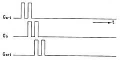
도 20은 본 발명의 제4 실시예에 따른 액정 표시 장치의 주사 신호의 파형도이다.20 is a waveform diagram of a scan signal of a liquid crystal display according to a fourth exemplary embodiment of the present invention.
도 21은 본 발명의 제5 실시예에 따른 액정 표시 장치의 회로도이다.21 is a circuit diagram of a liquid crystal display according to a fifth embodiment of the present invention.
도 22는 본 발명의 제5 실시예에 따른 액정 표시 장치의 화소의 극성을 표시한 개념도이다.FIG. 22 is a conceptual diagram illustrating polarities of pixels of a liquid crystal display according to a fifth exemplary embodiment of the present invention.
도 23은 본 발명의 제6 실시예에 따른 액정 표시 장치의 회로도이다.23 is a circuit diagram of a liquid crystal display according to a sixth embodiment of the present invention.
도 24는 본 발명의 제6 실시예에 따른 액정 표시 장치의 화소의 극성을 표시한 개념도이다.24 is a conceptual diagram illustrating the polarity of pixels of a liquid crystal display according to a sixth exemplary embodiment of the present invention.
도 25는 본 발명의 제7 실시예에 따른 액정 표시 장치의 회로도이다.25 is a circuit diagram of a liquid crystal display according to a seventh embodiment of the present invention.
본 발명은 액정 표시 장치에 관한 것으로서, 특히 광시야각을 얻기 위하여 화소 영역을 다수의 소 도메인으로 분할하는 수직 배향 액정 표시 장치에 관한 것이다.BACKGROUND OF THE
액정 표시 장치는 일반적으로 공통 전극과 컬러 필터(color filter) 등이 형성되어 있는 상부 기판과 박막 트랜지스터와 화소 전극 등이 형성되어 있는 하부 기판 사이에 액정 물질을 주입해 놓고 화소 전극과 공통 전극에 서로 다른 전위를 인가함으로써 전계를 형성하여 액정 분자들의 배열을 변경시키고, 이를 통해 빛의 투과율을 조절함으로써 화상을 표현하는 장치이다.In general, a liquid crystal display device injects a liquid crystal material between an upper substrate on which a common electrode, a color filter, and the like are formed, and a lower substrate on which a thin film transistor and a pixel electrode are formed. By applying a different potential to form an electric field to change the arrangement of the liquid crystal molecules, and through this to control the light transmittance is a device that represents the image.
그런데 액정 표시 장치는 시야각이 좁은 것이 중요한 단점이다. 이러한 단점을 극복하고자 시야각을 넓히기 위한 다양한 방안이 개발되고 있는데, 그 중에서도 액정 분자를 상하 기판에 대하여 수직으로 배향하고 화소 전극과 그 대향 전극인 공통 전극에 일정한 절개 패턴을 형성하거나 돌기를 형성하는 방법이 유력시되고 있다.However, it is an important disadvantage that the liquid crystal display device has a narrow viewing angle. In order to overcome these disadvantages, various methods for widening the viewing angle have been developed. Among them, liquid crystal molecules are oriented vertically with respect to the upper and lower substrates, and a method of forming a constant incision pattern or protrusion on the pixel electrode and the common electrode opposite thereto is performed. This is becoming potent.
절개 패턴을 형성하는 방법으로는 화소 전극과 공통 전극에 각각 절개 패턴을 형성하여 이들 절개 패턴으로 인하여 형성되는 프린지 필드(fringe field)를 이용하여 액정 분자들이 눕는 방향을 조절함으로써 시야각을 넓히는 방법이 있다.As a method of forming an incision pattern, an incision pattern is formed on each of the pixel electrode and the common electrode, and the viewing angle is widened by adjusting the direction in which the liquid crystal molecules lie down using a fringe field formed by the incision patterns. .
돌기를 형성하는 방법은 상하 기판 위에 형성되어 있는 화소 전극과 공통 전극 위에 각각 돌기를 형성해 둠으로써 돌기에 의하여 왜곡되는 전기장을 이용하여 액정 분자의 눕는 방향을 조절하는 방식이다.The method of forming the protrusions is a method of controlling the lying direction of the liquid crystal molecules by using the electric field distorted by the protrusions by forming protrusions on the pixel electrode and the common electrode formed on the upper and lower substrates, respectively.
또 다른 방법으로는, 하부 기판 위에 형성되어 있는 화소 전극에는 절개 패턴을 형성하고 상부 기판에 형성되어 있는 공통 전극 위에는 돌기를 형성하여 절개 패턴과 돌기에 의하여 형성되는 프린지 필드를 이용하여 액정의 눕는 방향을 조절함으로써 도메인을 형성하는 방식이 있다.In another method, an incision pattern is formed on the pixel electrode formed on the lower substrate, and a projection is formed on the common electrode formed on the upper substrate, so that the liquid crystal lies down using a fringe field formed by the incision pattern and the projection. There is a way to form a domain by controlling.
이러한 시야각을 넓히기 위한 다양한 방안 가운데 공통 전극에 절개 패턴을 형성하는 방법은, 공통 전극을 패터닝하기 위하여 별도의 마스크가 필요하고, 색 필터 위에 오버코트막이 없는 구조에서는 색 필터의 안료가 액정 물질에 영향을 주게 되므로 색 필터 위에 오버코트막을 형성하여야 하며, 패터닝된 전극의 가장자리에서 전경이 심하게 발생하는 등의 문제점이 존재한다. 또, 돌기를 형성하는 방법 역시 돌기를 형성하기 위한 별도의 공정을 필요로 하거나 기존의 공정을 변형시켜야 하므로 액정 표시 장치의 제조 방법을 복잡하게 만드는 문제점이 있다. 또한 돌기나 절개부로 인하여 개구율이 감소한다.Among various methods for widening the viewing angle, a method of forming an incision pattern on the common electrode requires a separate mask to pattern the common electrode, and in a structure without an overcoat layer on the color filter, the pigment of the color filter affects the liquid crystal material. As a result, an overcoat layer must be formed on the color filter, and the foreground is severely generated at the edge of the patterned electrode. In addition, the method of forming the projections also requires a separate process for forming the projections or the existing process has to be modified, there is a problem that complicates the manufacturing method of the liquid crystal display device. In addition, the aperture ratio decreases due to protrusions or incisions.
본 발명이 이루고자 하는 기술적 과제는 제조 공정이 복잡하지 않으면서 안정한 다중 도메인을 형성하는 액정 표시 장치를 제공하는 것이다.SUMMARY OF THE INVENTION The present invention has been made in an effort to provide a liquid crystal display device which forms a stable multiple domain without complicated manufacturing processes.
이러한 기술적 과제를 해결하기 위한 본 발명에 따른 화소 전극용 박막 트랜지스터와 방향 제어 전극용 박막 트랜지스터를 각각 형성하고 한 프레임 내에 2개의 펄스를 포함하는 주사 신호를 인가하여 구동한다.In order to solve the technical problem, a pixel electrode thin film transistor and a direction control electrode thin film transistor according to the present invention are formed, respectively, and are driven by applying a scan signal including two pulses in one frame.
구체적으로는, 절연 제1 기판, 상기 제1 기판 위에 형성되어 있는 제1 배선, 상기 제1 기판 위에 형성되어 있으며 상기 제1 배선과 절연되어 교차하고 있는 제2 배선, 상기 제1 배선과 상기 제2 배선이 교차하여 정의하는 화소 영역마다 형성되어 있는 화소 전극, 상기 제1 배선과 상기 제2 배선이 교차하여 정의하는 화소 영역마다 형성되어 있는 방향 제어 전극, 자기 단의 상기 제1 배선, 자기 단의 상기 제2 배선 및 상기 화소 전극과 연결되어 있는 제1 박막 트랜지스터, 전단의 상기 제1 배선, 전단 또는 후단의 상기 제2 배선 및 상기 방향 제어 전극과 연결되어 있는 제2 박막 트랜지스터, 상기 제1 기판과 마주보고 있는 절연 제2 기판, 상기 제2 기판에 형성되어 있는 공통 전극을 포함하는 액정 표시 장치를 마련한다.Specifically, an insulating first substrate, a first wiring formed on the first substrate, a second wiring formed on the first substrate and insulated from and intersecting the first wiring, the first wiring and the first wiring A pixel electrode formed for each pixel region defined by crossing two wirings, a direction control electrode formed for each pixel region defined by crossing the first wiring and the second wiring, the first wiring of a magnetic stage, and a magnetic stage A first thin film transistor connected to the second wiring and the pixel electrode of the second thin film transistor connected to the first wiring of the front end, the second wiring of the front end or the rear end and the direction control electrode of the first wiring A liquid crystal display device including an insulating second substrate facing the substrate and a common electrode formed on the second substrate is provided.
이 때, 액정 표시 장치는 점반전 구동을 하며, 상기 제1 배선에 인가되는 주사 신호는 한 프레임 내에 2개의 펄스를 포함한다. 또, 주사 신호의 한 프레임 내에 포함되는 2개의 펄스를 시간 순서에 따라 제1 펄스와 제2 펄스라고 할 때, 상기 제1 펄스는 전단의 제1 배선에 인가되는 주사 신호의 제2 펄스와 동기되어 있는 것이 바람직하다.In this case, the liquid crystal display performs dot inversion driving, and the scan signal applied to the first wiring includes two pulses in one frame. In addition, when two pulses included in one frame of the scan signal are referred to as the first pulse and the second pulse in time order, the first pulse is synchronized with the second pulse of the scan signal applied to the first wiring in the front end. It is preferable that it is done.
상기 화소 전극은 절개부를 가지고 있고, 상기 방향 제어 전극은 상기 화소 전극의 절개부와 적어도 일부가 중첩할 수 있다.The pixel electrode may have a cutout, and the direction control electrode may overlap at least a portion of the cutout of the pixel electrode.
또는, 절연 제1 기판, 상기 제1 기판 위에 형성되어 있는 제1 배선, 상기 제1 기판 위에 형성되어 있으며 상기 제1 배선과 절연되어 교차하고 있는 제2 배선, 상기 제1 배선과 상기 제2 배선이 교차하여 정의하는 화소 영역마다 형성되어 있는 화소 전극, 상기 제1 배선과 상기 제2 배선이 교차하여 정의하는 화소 영역마다 형성되어 있는 방향 제어 전극, 상기 화소 영역마다 형성되어 있는 제1 및 제2 박막 트랜지스터, 상기 제1 기판과 마주보고 있는 절연 제2 기판, 상기 제2 기판에 형성되어 있는 공통 전극을 포함하고, 상기 화소 영역은 상기 제1 박막 트랜지스터가 자기 단의 상기 제1 배선, 자기 단의 상기 제2 배선 및 상기 화소 전극과 연결되어 있고 상기 제2 박막 트랜지스터는 전단의 상기 제1 배선, 전단 또는 후단의 상기 제2 배선 및 상기 방향 제어 전극과 연결되어 있는 제1 화소 영역과 상기 제1 박막 트랜지스터가 자기 단의 상기 제1 배선, 자기 단의 상기 제2 배선 및 상기 화소 전극과 연결되어 있고 상기 제2 박막 트랜지스터는 전단의 상기 제1 배선, 자기 단의 상기 제2 배선 및 상기 방향 제어 전극과 연결되어 있는 제2 화소 영역으로 구분되는 액정 표시 장치를 마련한다.Alternatively, the insulating first substrate, the first wiring formed on the first substrate, the second wiring formed on the first substrate and insulated from and intersecting with the first wiring, the first wiring and the second wiring A pixel electrode formed for each of the pixel regions defined by the intersection, a direction control electrode formed for each pixel region of the first wiring and the second wiring, and the first and second electrodes formed for each of the pixel regions A thin film transistor, an insulating second substrate facing the first substrate, and a common electrode formed on the second substrate, wherein the pixel region includes: the first thin film transistor; Is connected to the second wiring and the pixel electrode of the second thin film transistor before the first wiring at the front end, the second wiring at the front end or the rear end, and before the direction control. A first pixel region connected to the first thin film transistor and the first thin film transistor are connected to the first wiring of the magnetic terminal, the second wiring of the magnetic terminal, and the pixel electrode, and the second thin film transistor is connected to the first wiring of the previous stage. And a liquid crystal display divided into a second pixel area connected to the second wiring and the direction control electrode of a magnetic terminal.
이 때, 액정 표시 장치는 2점 반전 구동을 하며, 상기 제1 배선에 인가되는 주사 신호는 한 프레임 내에 2개의 펄스를 포함하는 것이 바람직하다.In this case, it is preferable that the liquid crystal display performs two-point inversion driving, and the scan signal applied to the first wiring includes two pulses in one frame.
상기 제1 배선에 의하여 구분되는 화소 행은 상기 제1 화소 영역 행과 상기 제2 화소 영역 행으로 구분되고, 상기 제1 화소 영역 행과 상기 제2 화소 영역 행은 교대로 배치되어 있고, 2점 반전 구동시 동일한 극성이 되며 이웃하는 두 화소 영역은 게이트 신호가 인가되는 순서대로 제1 화소 영역 다음 제2 화소가 오도록 배치되어 있는 것이 바람직하다.The pixel row divided by the first wiring is divided into the first pixel region row and the second pixel region row, and the first pixel region row and the second pixel region row are alternately arranged, and two points are provided. In the inversion driving, two adjacent pixel areas having the same polarity are preferably arranged such that the second pixel comes after the first pixel area in the order in which the gate signal is applied.
또는, 절연 제1 기판, 상기 제1 기판 위에 형성되어 있는 제1 배선, 상기 제1 기판 위에 형성되어 있으며 상기 제1 배선과 절연되어 교차하고 있는 제2 배선, 상기 제1 배선과 상기 제2 배선이 교차하여 정의하는 화소 영역마다 형성되어 있는 화소 전극, 상기 제1 배선과 상기 제2 배선이 교차하여 정의하는 화소 영역마다 형성되어 있는 방향 제어 전극, 자기 단의 상기 제1 배선, 자기 단의 상기 제2 배선 및 상기 화소 전극과 연결되어 있는 제1 박막 트랜지스터, 전단의 상기 제1 배선, 자기 단의 상기 제2 배선 및 상기 방향 제어 전극과 연결되어 있는 제2 박막 트랜지스터, 상기 제1 기판과 마주보고 있는 절연 제2 기판, 상기 제2 기판에 형성 되어 있는 공통 전극을 포함하는 액정 표시 장치를 마련한다.Alternatively, the insulating first substrate, the first wiring formed on the first substrate, the second wiring formed on the first substrate and insulated from and intersecting with the first wiring, the first wiring and the second wiring A pixel electrode formed for each pixel region defined by the intersection, a direction control electrode formed for each pixel region defined by the first wiring and the second wiring, the first wiring of the magnetic stage, and the A first thin film transistor connected to a second wiring and the pixel electrode, the first wiring at a front end, the second wiring at a magnetic end, and a second thin film transistor connected to the direction control electrode, facing the first substrate. A liquid crystal display device including an insulating second substrate as viewed and a common electrode formed on the second substrate is provided.
이 때, 열 반전 구동을 하며, 상기 제1 배선에 인가되는 주사 신호는 한 프레임 내에 2개의 펄스를 포함하는 것이 바람직하다.At this time, the column inversion driving is performed, and the scan signal applied to the first wiring preferably includes two pulses in one frame.
또는, 절연 제1 기판, 상기 제1 기판 위에 형성되어 있는 제1 배선, 상기 제1 기판 위에 형성되어 있으며 상기 제1 배선과 절연되어 교차하고 있는 제2 배선, 상기 제2 배선과 절연되어 교차하고 있으며 공통 전압이 인가되는 제3 배선, 상기 제1 배선과 상기 제2 배선이 교차하여 정의하는 화소 영역마다 형성되어 있는 화소 전극, 상기 제1 배선과 상기 제2 배선이 교차하여 정의하는 화소 영역마다 형성되어 있는 방향 제어 전극, 자기 단의 상기 제1 배선, 자기 단의 상기 제2 배선 및 상기 화소 전극과 연결되어 있는 제1 박막 트랜지스터, 전단의 상기 제1 배선, 상기 제3 배선 및 상기 방향 제어 전극과 연결되어 있는 제2 박막 트랜지스터, 상기 제1 기판과 마주보고 있는 절연 제2 기판, 상기 제2 기판에 형성되어 있는 공통 전극을 포함하고, 상기 제1 배선에 인가되는 주사 신호는 한 프레임 내에 2개의 펄스를 포함하는 액정 표시 장치를 마련한다.Or an insulated first substrate, a first wiring formed on the first substrate, a second wiring formed on the first substrate and insulated from and intersecting with the first wiring, insulated from the second wiring, And a third wiring to which a common voltage is applied, a pixel electrode formed for each pixel region defined by crossing the first wiring and the second wiring, and a pixel region defined by crossing the first wiring and the second wiring. The formed direction control electrode, the first wiring at the magnetic stage, the second wiring at the magnetic stage, and the first thin film transistor connected to the pixel electrode, the first wiring at the front end, the third wiring, and the direction control. A second thin film transistor connected to the electrode, an insulated second substrate facing the first substrate, and a common electrode formed on the second substrate; Scan signal is provided to the liquid crystal display device including the two pulses within one frame.
첨부한 도면을 참고로 하여 본 발명의 실시예에 대하여 본 발명이 속하는 기술 분야에서 통상의 지식을 가진 자가 용이하게 실시할 수 있도록 상세히 설명한다.DETAILED DESCRIPTION Embodiments of the present invention will be described in detail with reference to the accompanying drawings so that those skilled in the art may easily implement the present invention.
도면에서 여러 층 및 영역을 명확하게 표현하기 위하여 두께를 확대하여 나타내었다. 명세서 전체를 통하여 유사한 부분에 대해서는 동일한 도면 부호를 붙였다. 층, 막, 영역, 판 등의 부분이 다른 부분 "위에" 있다고 할 때, 이는 다른 부분 "바로 위에" 있는 경우뿐 아니라 그 중간에 또 다른 부분이 있는 경우도 포함한다. 반대로 어떤 부분이 다른 부분 "바로 위에" 있다고 할 때에는 중간에 다른 부분이 없는 것을 뜻한다.In the drawings, the thickness of layers, films, panels, regions, etc., are exaggerated for clarity. Like parts are designated by like reference numerals throughout the specification. When a part of a layer, film, region, plate, etc. is said to be "on" another part, this includes not only the other part being "right over" but also another part in the middle. On the contrary, when a part is "just above" another part, there is no other part in the middle.
본 발명의 실시예에 따른 액정 표시 장치에 대하여 도면을 참고로 하여 상세하게 설명한다.A liquid crystal display according to an exemplary embodiment of the present invention will be described in detail with reference to the drawings.
그러면 도면을 참고로 하여 본 발명의 실시예에 따른 다중 도메인 액정 표시 장치에 대하여 설명한다.Next, a multi-domain liquid crystal display according to an exemplary embodiment of the present invention will be described with reference to the drawings.
도 1은 본 발명의 제1 실시예에 따른 액정 표시 장치의 회로도이다.1 is a circuit diagram of a liquid crystal display according to a first embodiment of the present invention.
본 발명의 제1 실시예에 따른 액정 표시 장치는 박막 트랜지스터 기판과, 이와 대향하는 색 필터 기판 및 이들 사이에 주입되어 있는 액정층으로 이루어져 있다. 박막 트랜지스터 기판에는 게이트선과 데이터선이 교차하여 화소 영역을 정의하고 있고, 기준 전위(Vcom)가 인가되는 유지 전극선이 게이트선과 나란하게 형성되어 있다. 이 때, 게이트선을 통하여는 주사 신호가 전달되고, 데이터선을 통하여는 화상 신호가 전달되며, 유지 전극선에는 기준 전위가 인가된다. 각 화소 영역에는 게이트선에 연결되어 있는 게이트 전극, 데이터선에 연결되어 있는 소스 전극 및 화소 전극에 드레인 전극이 연결되어 있는 화소 전극용 박막 트랜지스터(Pixel TFT)와 전단의 게이트선에 연결되어 있는 게이트 전극, 기준 전위가 인가되는 유지 전극선에 연결되어 있는 소스 전극 및 방향 제어 전극에 연결되어 있는 드레인 전극을 가지는 방향 제어 전극용 박막 트랜지스터(DCE TFT)가 하나씩 형성되어 있다. 방향 제어 전극은 화소 전극과 용량성 결합을 이루고 있고, 이들 사이의 정전 용량은 CDP라고 표시한다. 화소 전극은 색 필터 기판의 공통 전극과의 사이에 액정 축전기를 형성하고, 그 정전 용량은 CLC로 표시한다. 또, 화소 전극은 유지 전극선에 연결되어 있는 유지 전극과의 사이에 유지 축전기를 형성하고, 그 정전 용량은 CST로 표시한다.The liquid crystal display according to the first exemplary embodiment of the present invention includes a thin film transistor substrate, an opposing color filter substrate, and a liquid crystal layer injected therebetween. The thin film transistor substrate has a gate line and a data line intersecting to define a pixel region, and a sustain electrode line to which the reference potential Vcom is applied is formed in parallel with the gate line. At this time, a scan signal is transmitted through the gate line, an image signal is transmitted through the data line, and a reference potential is applied to the sustain electrode line. Each pixel region includes a gate electrode connected to a gate line, a source electrode connected to a data line, a pixel TFT for connecting a drain electrode to a pixel electrode, and a gate connected to a gate line of a previous stage. A thin film transistor (DCE TFT) for directional control electrodes having one electrode, a source electrode connected to the sustain electrode line to which a reference potential is applied, and a drain electrode connected to the direction control electrode is formed one by one. The direction control electrode forms a capacitive coupling with the pixel electrode, and the capacitance therebetween is denoted as CDP . The pixel electrode forms a liquid crystal capacitor between the common electrode of the color filter substrate, and the capacitance thereof is represented by CLC . In addition, the pixel electrode forms a storage capacitor between the storage electrodes connected to the storage electrode lines, and the capacitance thereof is represented by CST .
회로도에는 나타내지 못하였으나 본 발명에 따른 액정 표시 장치의 화소 전극은 절개부를 가지며, 이 절개부를 통하여 방향 제어 전극에 의한 전계가 유출될 수 있도록 방향 제어 전극과 절개부가 중첩되어 있다. 절개부를 통하여 유출되는 방향 제어 전극의 전계에 의하여 액정 분자가 선경사(pretilt)를 갖게되고, 선경사를 가지는 액정 분자는 화소 전극의 전계가 인가되면 흐트러짐 없이 신속하게 선경사에 의하여 결정된 방향으로 배향된다.Although not shown in the circuit diagram, the pixel electrode of the liquid crystal display according to the present invention has a cutout, and the direction control electrode and the cutout overlap each other so that an electric field by the direction control electrode can flow out through the cutout. The liquid crystal molecules have a pretilt by the electric field of the direction control electrode flowing out through the incision, and the liquid crystal molecules having the pretilt are oriented in the direction determined by the pretilt quickly without disturbing when the electric field of the pixel electrode is applied. do.
그런데 방향 제어 전극의 전계에 의하여 액정 분자가 선경사를 가지려면 공통 전극에 대한 방향 제어 전극의 전위차(이하 "방향 제어 전극 전압"이라 한다.)가 공통 전극에 대한 화소 전극의 전위차(이하 "화소 전극 전압"이라 한다.)에 비하여 소정의 값 이상으로 더 커야 한다. 본 발명에 따른 액정 표시 장치에서는 유지 전극선 전위를 방향 제어 전극에 인가한 후 화소 전극이 충전되는 시점부터는 방향 제어 전극을 부유 상태로 둠으로써 이러한 조건을 용이하게 만족시킬 수 있다. 그러면 그 이유에 대하여 설명한다.However, if the liquid crystal molecules have a pretilt due to the electric field of the direction control electrode, the potential difference of the direction control electrode (hereinafter referred to as "direction control electrode voltage") with respect to the common electrode is the potential difference of the pixel electrode with respect to the common electrode (hereinafter "pixel"). Electrode voltage ”, which is greater than a predetermined value. In the liquid crystal display according to the present invention, such a condition can be easily satisfied by applying the sustain electrode line potential to the direction control electrode and then leaving the direction control electrode in a floating state from the time when the pixel electrode is charged. Then, the reason will be explained.
주어진 화소 전극이 양의 전위로 리프레시(refresh)되는 순간을 생각해 보자. 리프레시 전에는 화소가 음의 전위로 충전되어 있을 것이고, 전단의 게이트에 온(on) 신호가 인가되면 방향 제어 전극용 박막 트랜지스터(DCE TFT)가 턴온되어 방향 제어 전극이 화소보다 전위가 높은 기준 전위로 충전된다. 이 때, 화소 전극도 방향 제어 전극과 용량성 결합을 이루고 있으므로 따라서 충전된다. 이 시점에서 방향 제어 전극과 화소 전극 사이의 정전 용량 CDP와 화소 전극과 공통 전극 사이의 정전 용량 CLC는 직렬로 연결되어 있는 상태가 된다. 화소 전극은 음의 전위를 가지고 있었으므로 방향 제어 전극용 박막 트랜지스터(DCE TFT)를 통한 직렬 충전시 방향 제어 전극보다 낮은 전위를 가지게 된다. 즉, VDCE > Vp 이다. 충전 후 방향 제어 전극용 박막 트랜지스터(DCE TFT)가 턴오프되면 방향 제어 전극은 부유(floating) 상태가 된다. 따라서 화소 전극 전위가 어떻게 변화하더라도 항상 방향 제어 전극 전위가 화소 전극 전위보다 높은 상태를 유지하게 된다. 즉, 화소 전극용 박막 트랜지스터(Pixel TFT)가 턴온되어서 화소 전극이 양의 전하로 충전되어 전위가 올라가면 방향 제어 전극의 전위도 화소 전극 전위와 일정한 전위차를 유지하며 동반 상승하게 된다. 이를 회로 관계식을 이용하여 설명하면 다음과 같다.Consider the moment when a given pixel electrode is refreshed with a positive potential. Before refreshing, the pixel will be charged to a negative potential. When the ON signal is applied to the gate of the previous stage, the direction control electrode thin film transistor (DCE TFT) is turned on so that the direction control electrode is set to a reference potential having a higher potential than the pixel. Is charged. At this time, the pixel electrode is also capacitively coupled with the direction control electrode and thus charged. At this point, the capacitance CDP between the direction control electrode and the pixel electrode and the capacitance CLC between the pixel electrode and the common electrode are connected in series. Since the pixel electrode has a negative potential, the pixel electrode has a lower potential than the direction control electrode in series charging through the thin film transistor (DCE TFT) for the direction control electrode. That is, VDCE > Vp . When the direction control electrode thin film transistor (DCE TFT) is turned off after charging, the direction control electrode is in a floating state. Therefore, no matter how the pixel electrode potential changes, the direction control electrode potential always remains higher than the pixel electrode potential. That is, when the pixel TFT thin TFT is turned on and the pixel electrode is charged with a positive charge, and the potential is increased, the potential of the direction control electrode is also raised while maintaining a constant potential difference with the pixel electrode potential. This is explained using a circuit relation as follows.
회로 내의 축전기 양단의 전압은The voltage across the capacitor in the circuit

로 표현된다. 그런데 축전기의 한쪽 전극이 부유 상태에 있다는 것은
따라서 음의 전압으로 리프레시(refresh)되는 경우에는 방향 제어 전극이 화소 전극보다 항상 소정의 값만큼 낮은 전위를 유지하게 된다.Therefore, when refreshed with a negative voltage, the direction control electrode always maintains a potential lower than the pixel electrode by a predetermined value.
본 발명에서는 DCE TFT를 유지 전극선에 연결하여 기준 전위가 방향 제어 전극에 인가될 수 있도록 한다. 따라서 다음 프레임에 화소 전극에 인가되는 전위의 극성이 무엇이냐에 관계없이 항상 두 전극의 전위가 동일한 극성으로 상승 또는 하강한다. 결국 본 발명은 선 반전 또는 점 반전 등의 구동 방식에 구애받지 않고 적용할 수 있다.In the present invention, the DCE TFT is connected to the sustain electrode line so that a reference potential can be applied to the direction control electrode. Therefore, regardless of the polarity of the potential applied to the pixel electrode in the next frame, the potentials of the two electrodes always rise or fall to the same polarity. After all, the present invention can be applied regardless of the driving method such as line inversion or point inversion.
또한 동일한 계조에서는 전후 프레임의 계조에 관계없이 방향 제어 전극과 화소 전극 사이의 전위차의 편차가 없어서 화질의 안정성이 높다.In addition, in the same gradation, there is no variation in the potential difference between the direction control electrode and the pixel electrode regardless of the gradation of the front and rear frame, so that the image quality is stable.
DCE TFT가 데이터선에 연결되지 않기 때문에 방향 제어 전극으로 인하여 데이터선의 부하가 증가하는 것을 방지할 수 있다.Since the DCE TFT is not connected to the data line, it is possible to prevent the load on the data line from increasing due to the direction control electrode.
그러면, 본 발명의 좀 더 구체적인 실시예를 도 2a 내지 2c를 이용하여 설명한다.A more specific embodiment of the present invention will now be described with reference to FIGS. 2A-2C.
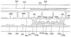
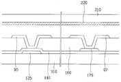
도 2a는 본 발명의 실시예에 따른 액정 표시 장치의 배치도이고, 도 2b와 도 2c는 각각 도 2a의 IIb-IIb'선과 IIc-IIc'선에 대한 단면도이다.2A is a layout view of a liquid crystal display according to an exemplary embodiment of the present invention, and FIGS. 2B and 2C are cross-sectional views taken along lines IIb-IIb 'and IIc-IIc' of FIG. 2A, respectively.
본 발명의 제1 실시예에 따른 액정 표시 장치는 하부 기판과 이와 마주보고 있는 상부 기판 및 하부 기판과 상부 기판 사이에 주입되어 기판에 수직으로 배향되어 있는 액정 물질로 이루어진다.The liquid crystal display according to the first exemplary embodiment of the present invention includes a lower substrate, an upper substrate facing the lower substrate, and a liquid crystal material injected between the lower substrate and the upper substrate and oriented perpendicular to the substrate.
그러면, 하부 기판에 대하여 좀 더 상세히 설명한다.Then, the lower substrate will be described in more detail.
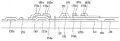
절연 기판(110) 위에 게이트선(121)이 형성되어 있고, 게이트선(121)과 교차하도록 데이터선(171)이 형성되어 있다. 게이트선(121)과 데이터선(171)은 서로 절연되어 있으며 이들이 교차하여 이루는 화소 영역에는 제1 게이트 전극(123a), 제1 소스 전극(173a) 및 제1 드레인 전극(175a)의 3단자를 가지는 화소 전극용 박막 트랜지스터와 제2 게이트 전극(123b), 제2 소스 전극(173b) 및 제2 드레인 전극(175b)의 3단자를 가지는 방향 제어 전극용 박막 트랜지스터가 하나씩 형성되어 있고, 방향 제어 전극(178)과 화소 전극(190)이 각각 형성되어 있다. 이 때, 화소 전극용 박막 트랜지스터는 화소 전극(190)을 스위칭하기 위한 것이고, 방향 제어 전극용 박막 트랜지스터는 방향 제어 전극(178)을 스위칭하기 위한 것이다. 화소 전극용 박막 트랜지스터의 게이트 전극(123a), 소스 전극(173a) 및 드레인 전극(175a)은 각각 해당 화소단의 게이트선(121), 데이터선(171) 및 화소 전극(190)에 연결되어 있다. 방향 제어 전극용 박막 트랜지스터의 게이트 전극(123b), 소스 전극(173b) 및 드레인 전극(175b)은 각각 전단의 게이트선(121), 해당 화소단의 유지 전극선(131) 및 방향 제어 전극(178)에 연결되어 있다. 방향 제어 전극(178)은 액정 분자의 선경사(pre-tilt)를 제어하기 위한 방향 제어 전압을 인가받아 공통 전극(270)과의 사이에 방향 제어 전계를 형성한다. 여기서 방향 제어 전극(178)은 데이터선(171)을 형성하는 단계에서 형성한다.The
하부 기판에 대하여 각 층 구조까지 고려하여 상세히 설명한다.The lower substrate will be described in detail considering each layer structure.
절연 기판(110) 위에 가로 방향으로 게이트선(121)이 형성되어 있고, 제1 및 제2 게이트 전극(123a, 123b)이 게이트선(121)에 연결되어 있다. 또 절연 기판(110) 위에는 유지 전극선(131)과 유지 전극(133a, 133b, 133c, 133d)이 형성되어 있다. 유지 전극선(131)은 가로 방향으로 뻗어 있고 제1 및 제2 유지 전극(133a, 133b)은 유지 전극선(131)으로부터 세로 방향으로 뻗어 있다. 제3 및 제4 유지 전극(133c, 133d)은 가로 방향으로 형성되어 있고 제1 유지 전극(133a)과 제2 유지 전극(133b)을 연결하고 있다. 게이트 배선(121, 123a, 123b) 및 유지 전극 배선(131, 133a, 133b, 133c, 133d)은 알루미늄 또는 그 합금, 크롬 또는 그 합금, 몰리브덴 또는 그 합금 등으로 이루어져 있으며, 필요에 따라서는 물리 화학적 특성이 우수한 Cr 또는 Mo 합금 등으로 이루어지는 제1층과, 저항이 작은 Al 또는 Ag 합금 등으로 이루어지는 제2층의 이중층으로 형성할 수도 있다.The
게이트 배선(121, 123a, 123b) 및 유지 전극 배선(131, 133a, 133b, 133c, 133d)의 위에는 게이트 절연막(140)이 형성되어 있다.The
게이트 절연막(140) 위에는 비정질 규소 등의 반도체로 이루어진 반도체층(151, 154a, 154b, 155)이 형성되어 있다. 반도체층(151, 154a, 154b, 155)은 박막 트랜지스터의 채널을 형성하는 제1 및 제2 채널부 반도체층(154a, 154b)과 데이터선(171) 아래에 위치하는 데이터선부 반도체층(151) 및 방향 제어 전극(178)과 유지 전극(133c, 133d)이 교차하는 부분에서 이들 금속 배선 사이의 절연을 보장하기 위한 교차부 반도체층(155)을 포함한다. 반도체층(151, 154a, 154b, 155)의 상부에는 실리사이드 또는 n형 불순물이 고농도로 도핑되어 있는 n+ 수소화 비정질 규소 따위의 물질로 만들어진 저항성 접촉층(161, 163a, 163b, 165a, 165b)이 각각 형성되어 있다.The semiconductor layers 151, 154a, 154b, and 155 made of a semiconductor such as amorphous silicon are formed on the
저항성 접촉층(161, 163a, 163b, 165a, 165b) 및 게이트 절연막(140) 위에는 데이터 배선(171, 173a, 173b, 175a, 175b)이 형성되어 있다. 데이터 배선(171, 173a, 173b, 175a, 175b)은 세로 방향으로 형성되어 있으며 게이트선(121)과 교차하여 화소를 정의하는 데이터선(171), 데이터선(171)의 분지이며 저항성 접촉층(163a)의 상부까지 연장되어 있는 제1 소스 전극(173a), 제1 소스 전극(173a)과 분리되어 있으며 제1 게이트 전극(123a)에 대하여 제1 소스 전극(173a)의 반대쪽 저항성 접촉층(165a) 상부에 형성되어 있는 제1 드레인 전극(175a), 제2 게이트 전극(123b) 상부에서 대향하고 있는 저항성 접촉층(163b, 165b) 위에 형성되어 있는 제2 소스 전극(173b) 및 제2 드레인 전극(175b)을 포함한다. 이 때, 데이터선(171)의 한쪽 끝은 외부 회로와 연결하기 위하여 폭이 확장되어 있다. 또 게이트선(121)과 데이터선(171)이 교차하여 이루는 화소 영역내에는 다수개의 X자 모양 금속편이 연결되어 이루어진 방향 제어 전극(178)이 형성되어 있다. 이 때, 방향 제어 전극(178)은 제2 드레인 전극(175b)과 연결되어 있다. 데이터 배선(171, 173a, 173b, 175a, 175b) 및 방향 제어 전극(178)은 알루미늄 또는 그 합금, 크롬 또는 그 합금, 몰리브덴 또는 그 합금 등으로 이루어져 있으며, 필요에 따라서는 물리 화학적 특성이 우수한 Cr 또는 Mo 합금 등으로 이루어지는 제1층과, 저항이 작은 Al 또는 Ag 합금 등으로 이루어지는 제2층의 이중층으로 형성할 수도 있다.The
데이터 배선(171, 173a, 173b, 175a, 175b) 위에는 질화 규소 또는 유기 절 연막으로 이루어진 보호막(180)이 형성되어 있다.A
보호막(180)에는 제1 드레인 전극을 드러내는 접촉구(181), 게이트 절연막(140)에도 걸쳐 형성되어 있으며 유지 전극선(131)을 드러내는 접촉구(182) 및 제2 소스 전극(173b)을 드러내는 접촉구(183)가 형성되어 있다.The
보호막(180) 위에는 접촉구(181)를 통하여 제1 드레인 전극(175a)과 연결되어 있으며 다수개의 X자 모양 절개부(191)와 직선형 절개부(192)를 가지는 화소 전극(190)이 형성되어 있다. 이 때, 다수개의 X자 모양 절개부(191)는 방향 제어 전극(178)의 X자 모양 부분과 중첩하고, 직선형 절개부(192)는 제3 및 제4 유지 용량 전극(133c, 133d)과 중첩한다. 방향 제어 전극(178)은 절개부(191)뿐만 아니라 화소 전극(190)의 절개부(191) 주변부와 넓게 중첩하고 있어서 화소 전극(190)과의 사이에 소정의 정전 용량을 가지는 축전기를 형성한다. 또 보호막(180) 위에는 접촉구(182, 183)를 통하여 유지 전극선(131)과 제2 소스 전극(173b)을 연결하는 소스 전극 연결 다리(92)가 형성되어 있다. 또한, 보호막(180) 위에는 접촉구를 통하여 각각 게이트선의 끝부분 및 데이터선의 끝부분과 연결되어 있는 접촉 보조 부재(도시하지 않음)가 형성되어 있다. 여기서, 화소 전극(190), 소스 전극 연결 다리(92) 및 접촉 보조 부재는 IZO(indium zinc oxide)로 이루어져 있다. 화소 전극(190), 소스 전극 연결 다리(92) 및 접촉 보조 부재는 ITO로 형성할 수도 있다.The
이상에서, 화소 전극(190)은 화소 영역을 다수의 소도메인으로 분할하기 위한 절개부 패턴(191, 192)을 가지며, 이중 제1 절개부(191)는 방향 제어 전극(178) 과 중첩되어 있고, 제2 절개부(192)는 유지 전극(133c, 133d)과 중첩되어 있다. 즉, 액정 표시 장치를 위에서 바라볼 때 방향 제어 전극(178)이 제1 절개부(191)를 통하여 노출되어 보이도록 방향 제어 전극(178)과 제1 절개부(191)를 배열한다. 또, 유지 전극선(131)과 방향 제어 전극(178) 사이에 방향 제어 전극용 박막 트랜지스터를 연결하고, 데이터선(171)과 화소 전극(190) 사이에 화소 전극용 박막 트랜지스터를 연결하며, 화소 전극(190)과 방향 제어 전극(178)은 용량성 결합을 이루도록 배치한다.In the above description, the
한편, 방향 제어 전극(178)은 게이트 배선(121, 123a, 123b)과 같은 층에 형성할 수도 있다. 또, 방향 제어 전극(178) 상부의 보호막(180)을 제거하여 트렌치를 형성할 수도 있다.The
상부 기판(210)에 대하여 좀 더 상세히 설명한다.The
유리 등의 투명한 절연 물질로 이루어진 상부 기판(210)의 아래 면에 빛샘을 방지하기 위한 블랙 매트릭스(220)와 적, 녹, 청의 색필터(230) 및 ITO 또는 IZO 등의 투명한 도전 물질로 이루어져 있는 공통 전극(270)이 형성되어 있다.It consists of a
액정층(3)에 포함되어 있는 액정 분자는 화소 전극(190)과 공통 전극(270) 사이에 전계가 인가되지 않은 상태에서 그 방향자가 하부 기판(110)과 상부 기판(210)에 대하여 수직을 이루도록 배향되어 있고, 음의 유전율 이방성을 가진다. 하부 기판(110)과 상부 기판(210)은 화소 전극(190)이 색필터(230)와 대응하여 정확하게 중첩되도록 정렬된다. 이렇게 하면, 화소 영역은 제1 및 제2 절개부(191, 192)에 의하여 다수의 소도메인으로 분할된다. 또, 방향 제어 전극(178)에 의하여 분할된 도메인 내에서 액정의 배향이 더욱 안정해진다.The liquid crystal molecules included in the
위에서는 액정 분자가 음의 유전율 이방성을 가지며 기판(110, 210)에 대하여 수직 배향되어 있는 경우를 예로 들었으나, 양의 유전율 이방성을 가지는 액정 분자를 기판(110, 210)에 대하여 수평 배향하여 액정층(3)을 형성할 수도 있다.In the above, the liquid crystal molecules have negative dielectric anisotropy and are vertically oriented with respect to the
이러한 구조의 액정 표시 장치에 있어서 박막 트랜지스터 기판을 제조하는 방법에 대하여 설명한다.A method of manufacturing a thin film transistor substrate in a liquid crystal display device having such a structure will be described.
도 3a 내지 도 3d는 본 발명의 제1 실시예에 따른 액정 표시 장치용 박막 트랜지스터 기판을 제조하는 과정을 순서대로 나타낸 단면도이다.3A to 3D are cross-sectional views sequentially illustrating a process of manufacturing a thin film transistor substrate for a liquid crystal display according to a first embodiment of the present invention.
먼저, 도 3a에 도시한 바와 같이, 금속 따위의 도전체층을 스퍼터링 따위의 방법으로 적층하고 마스크를 이용한 첫 번째 사진 식각 공정으로 건식 또는 습식 식각하여, 기판(110) 위에 게이트선(121, 125) 및 게이트 전극(123)을 포함하는 게이트 배선과 유지 전극선(131) 및 유지 전극(133a, 133b, 133c, 133d)을 포함하는 유지 배선을 형성한다.First, as shown in FIG. 3A, a conductive layer such as a metal is stacked by a method such as sputtering, and dry or wet etched by a first photolithography process using a mask to form
다음, 도 3b에 도시한 바와 같이, 게이트 절연막(140), 수소화 비정질 규소층 및 인(P) 따위의 n형 불순물이 고농도로 도핑되어 있는 비정질 규소층을 화학 기상 증착법을 이용하여 각각 1,500 Å 내지 5,000 Å, 500 Å 내지 2,000 Å, 300 Å 내지 600 Å의 두께로 연속 증착하고, 마스크를 이용한 사진 식각 공정으로 도핑된 비정질 규소층과 비정질 규소층을 차례로 패터닝하여 저항성 접촉층(160a, 160b, 161)과 비정질 규소층(151, 154a, 154b)을 형성한다.Next, as shown in FIG. 3B, each of the
이어, 도 3c에 도시한 바와 같이, 금속 따위의 도전체층을 스퍼터링 등의 방 법으로 1,500 Å 내지 3,000 Å의 두께로 증착한 다음 마스크를 이용한 사진 식각 공정으로 패터닝하여 데이터선(171), 소스 전극(173a, 173b), 드레인 전극(175a, 175b) 및 데이터 배선과 방향 제어 전극(178)을 형성한다. 이어, 소스 전극(173a, 173b)과 드레인 전극(175a, 175b)으로 가려지지 않은 저항성 접촉층(160a, 160b)을 식각하여 소스 전극(173a, 173b)과 드레인 전극(175a, 175b) 사이의 반도체층(151)을 드러내고 양쪽으로 분리된 저항성 접촉층(163a, 163b, 165a, 165b)을 형성한다.Subsequently, as illustrated in FIG. 3C, a conductive layer such as a metal is deposited to a thickness of 1,500 kV to 3,000 kV by sputtering or the like, and then patterned by a photolithography process using a mask to form a
이어, 도 3d에 나타낸 바와 같이, 낮은 유전율을 가지며, 평탄화 특성이 우수한 유기 절연 물질을 도포하거나 또는 4.0 이하의 낮은 유전율을 가지는 SiOF, SiOC 등과 같은 저유전율 절연 물질을 화학 기상 증착으로 적층하여 보호막(180)을 형성하고, 마스크를 이용한 사진 식각 공정으로 게이트 절연막(140)과 함께 패터닝하여, 접촉 구멍(181, 182, 183)을 형성한다.Next, as shown in FIG. 3D, a protective film may be formed by applying an organic insulating material having a low dielectric constant and excellent planarization characteristics or by depositing a low dielectric constant insulating material such as SiOF, SiOC, or the like having a low dielectric constant of 4.0 or less by chemical vapor deposition. 180 is formed and patterned together with the
마지막으로, 도 2a에 도시한 바와 같이, 400 Å 내지 500 Å 두께의 ITO 또는 IZO층을 증착하고 마스크를 이용한 사진 식각 공정으로 식각하여 화소 전극(190), 소스 전극 연결 다리(92) 및 접촉 보조 부재(도시하지 않음)를 형성한다.Lastly, as shown in FIG. 2A, the ITO or IZO layer having a thickness of 400 μs to 500 μs is deposited and etched by a photolithography process using a mask to etch the
이러한 방법은 앞에서 설명한 바와 같이, 5매의 마스크를 이용하는 제조 방법에 적용할 수 있지만, 4매 마스크를 이용하는 액정 표시 장치용 박막 트랜지스터 기판의 제조 방법에서도 동일하게 적용할 수 있다. 이에 대하여 도면을 참조하여 상세하게 설명하기로 한다.As described above, the method can be applied to a manufacturing method using five masks, but the same method can be applied to a manufacturing method of a thin film transistor substrate for a liquid crystal display device using four masks. This will be described in detail with reference to the drawings.
도 4는 본 발명의 제2 실시예에 따른 액정 표시 장치용 박막 트랜지스터 기 판의 배치도이고, 도 5는 도 4의 V-V'선 및 V'-V''선에 대한 단면도이다.4 is a layout view of a thin film transistor substrate for a liquid crystal display according to a second exemplary embodiment of the present invention, and FIG. 5 is a cross-sectional view taken along lines V-V ′ and V′-V ″ of FIG. 4.
제2 실시예에 따른 액정 표시 장치용 박막 트랜지스터 기판은 4매 마스크 공정으로 제조한 것으로서 5매 마스크 공정으로 제조한 박막 트랜지스터 기판에 비하여 다음과 같은 특징을 가진다.The thin film transistor substrate for a liquid crystal display according to the second embodiment is manufactured by a four-sheet mask process and has the following characteristics as compared with the thin film transistor substrate manufactured by a five-sheet mask process.
데이터선(171), 소스 전극(173a, 173b), 드레인 전극(175a, 175b)을 포함하는 데이터 배선과 방향 제어 전극(178) 하부에 이와 동일한 패턴으로 접촉층(161, 163a, 163b, 165a, 165b, 168)이 형성되어 있고, 제1 및 제2 소스 전극(173a, 173b)과 제1 및 제2 드레인 전극(175a, 175b) 사이의 채널부가 연결되어 있는 것을 제외하고 비정질 규소층(151, 154a, 154b, 158)도 데이터 배선 및 방향 제어 전극(178)과 동일한 패턴을 가진다. 기타 사항은 5매 마스크 공정에 의한 박막 트랜지스터 기판과 동일하다.The data lines including the
도 4에는 게이트선의 폭이 확장된 끝부분(125), 유지 전극선의 폭이 확장된 끝부분(135) 및 데이터선의 폭이 확장된 끝부분(179)과 함께 접촉 보조 부재(95, 99, 97)가 도시되어 있다.4 shows contact
그러면 이러한 구조적 특징을 가지는 박막 트랜지스터 기판의 제조 방법에 대하여 설명한다.Next, a method of manufacturing a thin film transistor substrate having such structural features will be described.
도 6a 내지 도 11b는 본 발명의 제2 실시예에 따른 액정 표시 장치용 박막 트랜지스터 기판을 제조하는 과정을 순서대로 나타낸 배치도 또는 단면도이다.6A to 11B are layout or cross-sectional views sequentially illustrating a process of manufacturing a thin film transistor substrate for a liquid crystal display according to a second exemplary embodiment of the present invention.
먼저, 도 6a 및 6b에 도시한 바와 같이, 제1 실시예와 동일하게 Al 또는 Ag 합금 등을 증착하고 사진 식각하여 게이트선(121, 125), 게이트 전극(123)을 포함 하는 게이트 배선과 유지 전극 배선(131, 133a, 133b, 133c, 133d)을 형성한다. (제1 마스크)First, as shown in FIGS. 6A and 6B, in the same manner as in the first embodiment, Al or Ag alloys or the like are deposited and photo-etched to form gate wirings including the
다음, 도 7에 도시한 바와 같이, 질화 규소로 이루어진 게이트 절연막(140), 비정질 규소층(150), n형 불순물로 고농도로 도핑된 비정질 규소로 이루어진 접촉층(160)을 화학 기상 증착법을 이용하여 각각 1,500 Å 내지 5,000 Å, 500 Å 내지 2,000 Å, 300 Å 내지 600 Å의 두께로 연속 증착하고, 이어 Al 또는 Ag 합금 등으로 이루어진 도전체층(170)을 스퍼터링 등의 방법으로 증착하고, 그 위에 감광막(PR)을 1㎛ 내지 2㎛의 두께로 도포한다.Next, as shown in FIG. 7, a chemical vapor deposition method is used for the
그 후, 마스크를 통하여 감광막(PR)에 빛을 조사한 후 현상하여, 도 8a 및 8b에 도시한 바와 같이, 감광막 패턴(PR)을 형성한다. 이때, 감광막 패턴(PR) 중에서 박막 트랜지스터의 채널부(C), 즉 소스 전극(173a, 173b)과 드레인 전극(175a, 175b) 사이에 위치한 부분은 데이터 배선부(A), 즉 데이터 배선이 형성될 부분에 위치한 부분보다 두께가 작게 되도록 하며, 기타 부분(B)의 감광막은 모두 제거한다. 이 때, 채널부(C)에 남아 있는 감광막의 두께와 데이터 배선부(A)에 남아 있는 감광막의 두께의 비는 후에 후술할 식각 공정에서의 공정 조건에 따라 다르게 하여야 하되, 전자의 두께를 후자의 두께의 1/2 이하로 하는 것이 바람직하며, 예를 들면, 4,000 Å 이하인 것이 좋다.(제2 마스크)Thereafter, the photoresist film PR is irradiated with light through a mask and then developed to form the photoresist pattern PR as shown in FIGS. 8A and 8B. At this time, a portion of the photoresist pattern PR that is positioned between the channel portion C of the thin film transistor, that is, between the
이와 같이, 위치에 따라 감광막의 두께를 달리하는 방법으로 여러 가지가 있을 수 있으며, A 영역의 빛 투과량을 조절하기 위하여 주로 슬릿(slit)이나 격자 형태의 패턴을 형성하거나 반투명막을 사용한다.As such, there may be various methods of varying the thickness of the photoresist layer according to the position. In order to control the light transmittance in the A region, a slit or lattice-shaped pattern is mainly formed or a translucent film is used.
이때, 슬릿 사이에 위치한 패턴의 선 폭이나 패턴 사이의 간격, 즉 슬릿의 폭은 노광시 사용하는 노광기의 분해능보다 작은 것이 바람직하며, 반투명막을 이용하는 경우에는 마스크를 제작할 때 투과율을 조절하기 위하여 다른 투과율을 가지는 박막을 이용하거나 두께가 다른 박막을 이용할 수 있다.In this case, the line width of the pattern located between the slits or the interval between the patterns, that is, the width of the slits, is preferably smaller than the resolution of the exposure machine used for exposure, and in the case of using a translucent film, the transmittance is different in order to control the transmittance when fabricating a mask. A thin film having a thickness or a thin film may be used.
이와 같은 마스크를 통하여 감광막에 빛을 조사하면 빛에 직접 노출되는 부분에서는 고분자들이 완전히 분해되며, 슬릿 패턴이나 반투명막이 형성되어 있는 부분에서는 빛의 조사량이 적으므로 고분자들은 완전 분해되지 않은 상태이며, 차광막으로 가려진 부분에서는 고분자가 거의 분해되지 않는다. 이어 감광막을 현상하면, 고분자 분자들이 분해되지 않은 부분만이 남고, 빛이 적게 조사된 중앙 부분에는 빛에 전혀 조사되지 않은 부분보다 얇은 두께의 감광막이 남길 수 있다. 이때, 노광 시간을 길게 하면 모든 분자들이 분해되므로 그렇게 되지 않도록 해야 한다.When the light is irradiated to the photosensitive film through such a mask, the polymers are completely decomposed at the part directly exposed to the light, and the polymers are not completely decomposed because the amount of light is small at the part where the slit pattern or the translucent film is formed. In the area covered by, the polymer is hardly decomposed. Subsequently, when the photoresist film is developed, only a portion where the polymer molecules are not decomposed is left, and a thin photoresist film may be left at a portion where the light is not irradiated at a portion less irradiated with light. In this case, if the exposure time is extended, all molecules are decomposed, so it should not be so.
이러한 얇은 두께의 감광막은 리플로우가 가능한 물질로 이루어진 감광막을 도포하고 빛이 완전히 투과할 수 있는 부분과 빛이 완전히 투과할 수 없는 부분으로 나뉘어진 통상적인 마스크를 사용하여 노광한 다음, 현상하고 리플로우시켜 감광막이 잔류하지 않는 부분으로 감광막의 일부를 흘러내리도록 함으로써 형성할 수도 있다.This thin photoresist film is applied using a conventional mask that is coated with a photoresist film made of a reflowable material and divided into a part that can completely transmit light and a part that can't completely transmit light, and then develop and ripple. It can also be formed by letting a part of the photosensitive film flow to the part which does not remain by making it low.
이어, 감광막 패턴(PR) 및 그 하부의 막들, 즉 도전체층(170), 접촉층(160) 및 반도체층(150)에 대한 식각을 진행한다. 이때, 데이터 배선부(A)에는 데이터 배선 및 그 하부의 막들이 그대로 남아 있고, 채널부(C)에는 반도체층만 남아 있어 야 하며, 나머지 부분(B)에는 위의 3개 층(150, 160, 170)이 모두 제거되어 게이트 절연막(140)이 드러나야 한다.Subsequently, etching is performed on the photoresist pattern PR and the lower layers thereof, that is, the
먼저, 도 9에 도시한 것처럼, 기타 부분(B)의 노출되어 있는 도전체층(170)을 제거하여 그 하부의 중간층(160)을 노출시킨다. 이 과정에서는 건식 식각 또는 습식 식각 방법을 모두 사용할 수 있으며, 이때 도전체층(170)은 식각되고 감광막 패턴(PR)은 거의 식각되지 않는 조건 하에서 행하는 것이 좋다. 그러나, 건식 식각의 경우 도전체층(170)만을 식각하고 감광막 패턴(PR)은 식각되지 않는 조건을 찾기가 어려우므로 감광막 패턴(PR)도 함께 식각되는 조건 하에서 행할 수 있다. 이 경우에는 습식 식각의 경우보다 채널부(C) 감광막의 두께를 두껍게 하여 이 과정에서 채널부(C) 감광막이 제거되어 하부의 도전체층(170)이 드러나는 일이 생기지 않도록 한다.First, as shown in FIG. 9, the exposed
이렇게 하면, 도 9에 나타낸 것처럼, 채널부(C) 및 데이터 배선부(B)의 도전체층(171, 170a, 170b)과 방향 제어 전극(178)만이 남고 기타 부분(B)의 도전체층은 모두 제거되어 그 하부의 접촉층(160)이 드러난다. 이때 남은 데이터 배선부 도전체 패턴(171, 170a, 170b)은 소스 및 드레인 전극(173a, 173b, 175a, 175b)이 분리되지 않고 연결되어 있는 점을 제외하면 데이터 배선(171, 173a, 173b, 175a, 175b, 179)의 형태와 동일하다. 또한 건식 식각을 사용한 경우 감광막 패턴(PR)도 어느 정도의 두께로 식각된다.In this way, as shown in FIG. 9, only the conductor layers 171, 170a, 170b and the
이어, 도 10에 도시한 바와 같이, 기타 부분(B)의 노출된 접촉층(160) 및 그 하부의 비정질 규소층(150)을 채널부(C) 감광막과 함께 건식 식각 방법으로 동시에 제거한다. 이 때의 식각은 감광막 패턴(PR)과 접촉층(160) 및 반도체층(150)(반도체층과 접촉층은 식각 선택성이 거의 없음)이 동시에 식각되며 게이트 절연막(140)은 식각되지 않는 조건 하에서 행하여야 하며, 특히 감광막 패턴(PR)과 반도체층(150)에 대한 식각비가 거의 동일한 조건으로 식각하는 것이 바람직하다. 예를 들어, SF6과 HCl의 혼합 기체나, SF6과 O2의 혼합 기체를 사용하면 거의 동일한 식각율로 두 막을 식각할 수 있다. 감광막 패턴(PR)과 반도체층(150)에 대한 식각율이 동일한 경우 채널부(C) 감광막의 두께는 반도체층(150)과 중간층(160)의 두께를 합한 것과 같거나 그보다 작아야 한다.Next, as shown in FIG. 10, the exposed
이렇게 하면, 도 10에 나타낸 바와 같이, 채널부(C)의 감광막이 제거되어 소스/드레인용 도전체 패턴(170a, 170b)이 드러나고, 기타 부분(B)의 접촉층(160) 및 반도체층(150)이 제거되어 그 하부의 게이트 절연막(140)이 드러난다. 한편, 데이터 배선부(A)의 감광막 역시 식각되므로 두께가 얇아진다. 또한, 이 단계에서 반도체층 패턴(151, 154a, 154b, 158)이 완성된다. 반도체층 패턴(151, 154a, 154b, 158)의 위에는 접촉층(161, 160a, 160b, 168)이 형성되어 있다.In this case, as shown in FIG. 10, the photosensitive film of the channel portion C is removed to expose the source /
이어 애싱(ashing)을 통하여 채널부(C)의 소스/드레인용 도전체 패턴(170a, 170b)의 채널부(C) 표면에 남아 있는 감광막 찌꺼기를 제거한다.Subsequently, ashing of the photoresist film remaining on the surface of the channel portion C of the source /
다음, 도 11a 및 11b에 도시한 바와 같이 채널부(C)의 소스/드레인용 도전체 패턴(170a, 170b) 및 그 하부의 소스/드레인용 접촉층 패턴(160a, 160b)을 식각하여 제거한다. 이 때, 식각은 소스/드레인용 도전체 패턴(170a, 170b)과 접촉층 패 턴(160a, 160b) 모두에 대하여 건식 식각만으로 진행할 수도 있으며, 소스/드레인용 도전체 패턴(170a, 170b)에 대해서는 습식 식각으로, 접촉층 패턴(160a, 160b)에 대해서는 건식 식각으로 행할 수도 있다. 전자의 경우 소스/드레인용 도전체 패턴(170a, 170b)과 접촉층 패턴(160a, 160b)의 식각 선택비가 큰 조건 하에서 식각을 행하는 것이 바람직하며, 이는 식각 선택비가 크지 않을 경우 식각 종점을 찾기가 어려워 채널부(C)에 남는 반도체 패턴(154a, 154b)의 두께를 조절하기가 쉽지 않기 때문이다. 습식 식각과 건식 식각을 번갈아 하는 후자의 경우에는 습식 식각되는 소스/드레인용 도전체 패턴(170a, 170b)의 측면은 식각되지만, 건식 식각되는 접촉층 패턴(160a, 160b)은 거의 식각되지 않으므로 계단 모양으로 만들어진다. 접촉층(160a, 160b) 및 반도체 패턴(151a, 151b)을 식각할 때 사용하는 식각 기체의 예로는 CF4와 HCl의 혼합 기체나 CF4와 O2의 혼합 기체를 들 수 있으며, CF4와 O2를 사용하면 균일한 두께로 반도체 패턴(154a, 154b)을 남길 수 있다. 이때, 반도체 패턴(154a, 154b)의 일부가 제거되어 두께가 작아질 수도 있으며 데이터 배선부(A) 감광막(PR)도 이때 어느 정도의 두께로 식각된다. 이때의 식각은 게이트 절연막(140)이 식각되지 않는 조건으로 행하여야 하며, 데이터 배선부(A) 감광막(PR)이 식각되어 그 하부의 데이터 배선(171, 173a, 173b, 175a, 175b, 179) 및 방향 제어 전극(178)이 드러나는 일이 없도록 감광막 패턴이 두꺼운 것이 바람직함은 물론이다.Next, as illustrated in FIGS. 11A and 11B, the source /
이렇게 하면, 소스 전극(173a, 173b)과 드레인 전극(175a, 175b)이 분리되면 서 데이터 배선(171, 173a, 173b, 175a, 174b, 179)과 그 하부의 접촉층 패턴(161, 163a, 163b, 165a, 165b)이 완성된다.In this case, the
마지막으로 데이터 배선부(A) 감광막을 제거한다. 그러나, 데이터 배선부(A) 감광막의 제거는 채널부(C) 소스/드레인용 도전체 패턴(170a, 170b)을 제거한 후 그 밑의 접촉층 패턴(160a, 160b)을 식각하기 전에 이루어질 수도 있다.Finally, the data wiring part A photosensitive film is removed. However, the removal of the data wiring part A photosensitive film may be performed after removing the
앞에서 설명한 것처럼, 습식 식각과 건식 식각을 교대로 하거나 건식 식각만을 사용할 수 있다. 후자의 경우에는 한 종류의 식각만을 사용하므로 공정이 비교적 간편하지만, 알맞은 식각 조건을 찾기가 어렵다. 반면, 전자의 경우에는 식각 조건을 찾기가 비교적 쉬우나 공정이 후자에 비하여 번거로운 점이 있다.As mentioned earlier, wet and dry etching can be alternately used or only dry etching can be used. In the latter case, since only one type of etching is used, the process is relatively easy, but it is difficult to find a suitable etching condition. On the other hand, in the former case, the etching conditions are relatively easy to find, but the process is more cumbersome than the latter.
다음, 도 4 및 도 5에 도시한 바와 같이, a-Si:C:O 막 또는 a-Si:O:F 막을 화학 기상 증착(CVD) 법에 의하여 성장시키거나 질화규소 등의 무기 절연 물질을 증착하거나 또는 아크릴계 물질 등의 유기 절연 물질을 도포하여 보호막(180)을 형성한다. 이 때, a-Si:C:O 막의 경우에는 기체 상태의 SiH(CH3)3, SiO2(CH3)4, (SiH)4O4(CH3)4, Si(C2H5O)4등을 기본 소스로 사용하고, N2O 또는 O2 등의 산화제와 Ar 또는 He 등을 혼합한 기체를 흘리면서 증착한다. 또, a-Si:O:F 막의 경우에는 SiH4, SiF4 등에 O2를 첨가한 기체를 흘리면서 증착한다. 이 때, 불소의 보조 소스로서 CF4를 첨가할 수도 있다.Next, as shown in FIGS. 4 and 5, an a-Si: C: O film or an a-Si: O: F film is grown by chemical vapor deposition (CVD) or an inorganic insulating material such as silicon nitride is deposited. Alternatively, the
이어, 도 4 및 도 5에 도시한 바와 같이, 보호막(180)을 게이트 절연막(140)과 함께 사진 식각하여 제1 드레인 전극(175a), 제2 소스 전극(173b), 유지 전극선(131), 게이트선의 폭이 확장된 끝부분(125), 유지 전극선의 폭이 확장된 끝부분(135) 및 데이터선의 폭이 확장된 끝부분(179)을 각각 드러내는 접촉구(181, 182, 183, 184, 185, 186)를 형성한다. 이때, 각 선의 끝부분(125, 179, 135)을 드러내는 접촉구(184, 185, 186)의 면적은 2mm×60㎛를 넘지 않으며, 0.5mm×15㎛ 이상인 것이 바람직하다. (제3 마스크)4 and 5, the
마지막으로, 400 Å 내지 500 Å 두께의 ITO층 또는 IZO층을 증착하고 사진 식각하여 드레인 전극(175)과 연결되는 화소 전극(190), 게이트선의 끝부분(125)과 연결된 접촉 보조 부재(95), 데이터선의 끝부분(179)과 연결된 접촉 보조 부재(97) 및 제2 소스 전극(173b)과 유지 전극선(131)을 연결하는 소스 전극 연결 다리(92)를 형성한다. (제4 마스크)Finally, the
이때, 화소 전극(190), 접촉 보조 부재(95, 97) 및 소스 전극 연결 다리(92)를 IZO로 형성하는 경우에는 식각액으로 크롬 식각액을 사용할 수 있어서 이들을 형성하기 위한 사진 식각 과정에서 접촉구를 통해 드러난 데이터 배선이나 게이트 배선 금속이 부식되는 것을 방지할 수 있다. 이러한 크롬 식각액으로는 (HNO3/(NH4)2Ce(NO3)6/H2O) 등이 있다. 또한, 접촉부의 접촉 저항을 최소화하기 위해서는 IZO를 상온에서 200℃ 이하의 범위에서 적층하는 것이 바람직하며, IZO 박막을 형성하기 위해 사용하는 표적(target)은 In2O3 및 ZnO를 포함하는 것이 바람직하며, ZnO의 함유량은 15-20 at% 범위인 것이 바람직하다.In this case, when the
한편, ITO나 IZO를 적층하기 전의 예열(pre-heating) 공정에서 사용하는 기 체로는 질소를 사용하는 것이 바람직하며, 이는 접촉구(181, 182, 183, 184, 185, 186)를 통해 드러난 금속막의 상부에 금속 산화막이 형성되는 것을 방지하기 위함이다.On the other hand, as a gas used in the pre-heating process before laminating ITO or IZO, it is preferable to use nitrogen, which is a metal exposed through the contact holes 181, 182, 183, 184, 185, and 186. This is to prevent the metal oxide film from being formed on top of the film.
도 12는 도 2a 및 도 4로 표현된 본 발명의 실시예에 따른 액정 표시 장치용 박막 트랜지스터 기판의 구성을 간략화하여 표시한 것이다.FIG. 12 is a simplified diagram illustrating a configuration of a thin film transistor substrate for a liquid crystal display according to an exemplary embodiment of the present invention, which is represented by FIGS. 2A and 4.
이상과 같이 유지 전극선에 연결된 박막 트랜지스터로 방향 제어 전극(178)을 스위칭하고, 데이터선(171)에 연결된 박막 트랜지스터로 화소 전극(190)을 스위칭하며, 화소 전극(190)과 방향 제어 전극(178)은 용량성 결합을 이루도록 함으로써 동일한 계조에서는 화소 전극(190)과 방향 제어 전극(178) 사이의 전위차의 편차가 없도록 한다. 따라서 안정적인 휘도 구현이 가능하고, 선반전 구동이나 점반전 구동 등 구동 방법에 구애받지 않는다.As described above, the
본 발명의 제1 및 제2 실시예에서는 방향 제어 전극용 박막 트랜지스터의 소스 전극이 유지 전극선에 연결되어 있으나 이와 달리 전단의 데이터선에 연결할 수도 있다. 이러한 구조에서는 다음과 같은 문제점이 있다.In the first and second embodiments of the present invention, the source electrode of the thin film transistor for direction control electrode is connected to the sustain electrode line. Alternatively, the source electrode of the thin film transistor for direction control electrode may be connected to the data line of the front end. This structure has the following problems.
먼저, 전단의 게이트선(도 1에서 Gate N-1)에 온(on) 전압이 인가됨에 의하여 대각선 방향에 위치하는 화소 전극에 계조 전압이 충전되는 것과 동시에 방향 제어 전극에 초기 전압이 충전된다. 따라서 방향 제어 전극의 초기 전압은 대각선 방향 화소의 계조 전압과 같게 된다. 이 때문에 대각선 방향 화소의 계조에 따라 방향 제어 전극과 화소 전극 사이의 전압차인 VDP가 결정된다. 따라서, 대각선 화 소에 블랙(black) 전압 등의 낮은 계조가 인가되는 경우에는 방향 제어 전극의 초기 전압도 동일하게 낮은 값을 가지게 되고, VDP도 낮은 값을 가지게 된다. VDP가 낮다는 것은 방향 제어 전극과 화소 전극 사이의 전압차가 작다는 것으로 이렇게 되면 방향 제어 전극에 의한 횡방향 전계(lateral field)가 약해져 액정의 배열이 불안정하게 되고, 이로 인하여 텍스쳐가 불안정하게 된다. 빠른 응답 속도를 위하여는 텍스쳐의 안정성이 요구되고 이를 위하여는 VDP가 5V 이상의 높은 값을 가져야 한다.First, the on-voltage is applied to the gate line (Gate N-1 in FIG. 1) of the front end, and the initial voltage is charged to the direction control electrode while the gray voltage is charged to the pixel electrode positioned in the diagonal direction. Therefore, the initial voltage of the direction control electrode is equal to the gray voltage of the diagonal pixel. For this reason, a difference between the voltage VDP between direction control electrode and the pixel electrode is determined in accordance with the gray level of the pixel diagonally. Therefore, when a low gray level such as a black voltage is applied to the diagonal pixels, the initial voltage of the direction control electrode has the same low value, and the VDP also has a low value. The low VDP means that the voltage difference between the direction control electrode and the pixel electrode is small. In this case, the lateral field caused by the direction control electrode is weakened, resulting in unstable alignment of the liquid crystals, resulting in unstable texture. . For fast response speed, texture stability is required, and for this, VDP should have a high value of 5V or more.
다음, VDP는 대각선 방향 화소의 계조 전압이 CDP와 (CLC+CST)가 직렬 연결되어 있는 회로에 인가되어 분압될 때, CDP에 걸리는 전압으로 결정된다. 따라서, VDP는 CDP가 작을수록 큰 값을 가지게 된다. 따라서 CDP를 작게 하기 위하여 화소 전극과 방향 제어 전극과의 중첩 면적이 최소화되도록 설계하는데, 이렇게 되면 제조 공정에서 발생하는 마스크의 오정렬에 의하여 화질이 민감하게 변화하고, 방향 제어 전극 주변에서 빛샘이 발생할 수도 있다. 전자는 마스크의 오정렬에 의하여 화소 전극과 방향 제어 전극의 중첩 면적이 변화하는데 이러한 변화가 직접적으로 화질에 영향을 미치기 때문이다. 후자는 방향 제어 전극의 초기 전압으로 높은 전압이 인가(대각선 방향 화소에 높은 계조 전압이 인가된 경우)되고, 자기 화소에 블랙 전압이 인가되면 방향 제어 전극의 높은 전압에 의하여 액정이 구동되어 빛이 샐 수 있는 상태가 되는데, 방향 제어 전극의 폭이 좁기 때문에 이를 차단하지 못하여 방 향 제어 전극 주변에서 빛샘이 발생한다. 이러한 빛샘이 발생하면 대비비가 낮아진다.Next, VDP is determined as the voltage applied to the CDP when the gray scale voltage of the diagonal pixel is applied to the circuit where CDP and (CLC + CST ) are connected and divided. Therefore, the VDP has a larger value as the CDP is smaller. Therefore, in order to reduce the CDP , the overlapping area between the pixel electrode and the direction control electrode is minimized. In this case, the image quality is sensitively changed by the misalignment of the mask generated in the manufacturing process, and light leakage occurs around the direction control electrode. It may be. The former changes the overlapping area of the pixel electrode and the direction control electrode due to misalignment of the mask because this change directly affects the image quality. The latter is applied to the initial voltage of the direction control electrode (when a high gradation voltage is applied to the diagonal pixel), and when a black voltage is applied to the magnetic pixel, the liquid crystal is driven by the high voltage of the direction control electrode to emit light. It is in a state where it can be leaked. Since the width of the direction control electrode is narrow, it cannot be blocked and light leakage occurs around the direction control electrode. When such light leakage occurs, the contrast ratio is lowered.
이하에서 설명하는 제3 실시예를 이러한 문제를 해결하고 있다.The third embodiment described below solves this problem.
도 13은 본 발명의 제3 실시예에 따른 액정 표시 장치의 회로도다.13 is a circuit diagram of a liquid crystal display according to a third embodiment of the present invention.
본 발명의 실시예에 따른 액정 표시 장치는 박막 트랜지스터 기판과, 이와 대향하는 색 필터 기판 및 이들 사이에 주입되어 있는 액정층으로 이루어져 있다. 박막 트랜지스터 기판에는 게이트선과 데이터선이 교차하여 화소 영역을 정의하고 있고, 기준 전위(Vcom)가 인가되는 유지 전극선이 게이트선과 나란하게 형성되어 있다. 이 때, 게이트선을 통하여는 주사 신호가 전달되고, 데이터선을 통하여는 화상 신호가 전달되며, 유지 전극선에는 기준 전위가 인가된다. 각 화소 영역에는 게이트선에 연결되어 있는 게이트 전극, 데이터선에 연결되어 있는 소스 전극 및 화소 전극에 드레인 전극이 연결되어 있는 화소 전극용 박막 트랜지스터(Pixel TFT), 전단의 게이트선에 연결되어 있는 게이트 전극, 전단의 데이터선에 연결되어 있는 소스 전극 및 방향 제어 전극에 연결되어 있는 드레인 전극을 가지는 제1 방향 제어용 박막 트랜지스터(DCE TFT1) 및 전단의 게이트선에 연결되어 있는 게이트 전극, 자기 단의 데이터선에 연결되어 있는 소스 전극 및 화소 전극에 연결되어 있는 드레인 전극을 가지는 제2 방향 제어용 박막 트랜지스터(DCE TFT2)가 각각 하나씩 형성되어 있다. 방향 제어 전극은 화소 전극과 용량성 결합을 이루고 있고, 이들 사이의 정전 용량은 CDP라고 표시한다. 화소 전극은 색 필터 기판의 공통 전극 과의 사이에 액정 축전기를 형성하고, 그 정전 용량은 CLC로 표시한다. 또, 화소 전극은 유지 전극선에 연결되어 있는 유지 전극과의 사이에 유지 축전기를 형성하고, 그 정전 용량은 CST로 표시한다.The liquid crystal display according to the exemplary embodiment of the present invention includes a thin film transistor substrate, an opposite color filter substrate, and a liquid crystal layer injected therebetween. The thin film transistor substrate has a gate line and a data line intersecting to define a pixel region, and a sustain electrode line to which the reference potential Vcom is applied is formed in parallel with the gate line. At this time, a scan signal is transmitted through the gate line, an image signal is transmitted through the data line, and a reference potential is applied to the sustain electrode line. Each pixel region includes a gate electrode connected to a gate line, a source electrode connected to a data line, a pixel TFT for connecting a drain electrode to a pixel electrode, and a gate connected to a gate line of a front end. Data of the first direction control thin film transistor (DCE TFT1) having an electrode, a source electrode connected to the data line at the front end, and a drain electrode connected to the direction control electrode, a gate electrode connected to the gate line at the front end, and data of the magnetic stage. Each of the second direction control thin film transistors DCE TFT2 having a source electrode connected to a line and a drain electrode connected to a pixel electrode is formed. The direction control electrode forms a capacitive coupling with the pixel electrode, and the capacitance therebetween is denoted as CDP . The pixel electrode forms a liquid crystal capacitor between the common electrode of the color filter substrate, and the capacitance thereof is represented by CLC . In addition, the pixel electrode forms a storage capacitor between the storage electrodes connected to the storage electrode lines, and the capacitance thereof is represented by CST .
회로도에는 나타내지 못하였으나 본 발명에 따른 액정 표시 장치의 화소 전극은 절개부를 가지며, 이 절개부를 통하여 방향 제어 전극에 의한 전계가 유출될 수 있도록 방향 제어 전극과 절개부가 중첩되어 있다. 절개부를 통하여 유출되는 방향 제어 전극의 전계에 의하여 액정 분자가 선경사(pretilt)를 갖게되고, 선경사를 가지는 액정 분자는 화소 전극의 전계가 인가되면 흐트러짐 없이 신속하게 선경사에 의하여 결정된 방향으로 배향된다.Although not shown in the circuit diagram, the pixel electrode of the liquid crystal display according to the present invention has a cutout, and the direction control electrode and the cutout overlap each other so that an electric field by the direction control electrode can flow out through the cutout. The liquid crystal molecules have a pretilt by the electric field of the direction control electrode flowing out through the incision, and the liquid crystal molecules having the pretilt are oriented in the direction determined by the pretilt quickly without disturbing when the electric field of the pixel electrode is applied. do.
이러한 구조의 액정 표시 장치에 점반전 구동을 적용하면, 전단 게이트선(Gate N-1)의 온 신호에 의하여 DCE TFT1과 DCE TFT2가 함께 온되어 방향 제어 전극에는 양(+)극성의 계조 전압이 충전되고, 화소 전극에는 음(-)극성의 계조 전압이 충전된다. 따라서 방향 제어 전극의 초기 전압(VDP)은 Data A와 Data B로부터 인가되는 양극성 계조 전압과 음극성 계조 전압간의 차가 되므로 DCE TFT2를 형성하지 않은 경우에 비하여 적어도 2배 이상 높은 VDP를 얻을 수 있다. 이후, 자기 단의 게이트선(Gate N)에 온 신호가 인가되어 Pixel TFT가 온될 때는 DCE TFT1과 DCE TFT2는 모두 오프되어 방향 제어 전극이 부유 상태에 있게 되므로 방향 제어 전극 전압은 화소 전극에 충전되는 전압과 VDP만큼의 차를 유지하며 함께 상승 하게 된다. 이와 같이, 제3 실시예에 따른 구조는 보다 높은 VDP를 확보함으로써 액정 배열의 안정성을 높여 텍스쳐를 안정화할 수 있다.When the point inversion driving is applied to the liquid crystal display having such a structure, the DCE TFT1 and the DCE TFT2 are turned on together by the ON signal of the front gate line Gate N-1, so that the gray scale voltage of the positive polarity is applied to the direction control electrode. The pixel electrode is charged with a negative polarity gray scale voltage. Therefore, since the initial voltage VDP of the direction control electrode is the difference between the positive gray voltage and the negative gray voltage applied from Data A and Data B, at least two times higher VDP can be obtained than when the DCE TFT2 is not formed. have. Then, when the ON signal is applied to the gate line Gate N of the magnetic stage and the pixel TFT is turned on, both the DCE TFT1 and the DCE TFT2 are turned off so that the direction control electrode is in a floating state, and thus the direction control electrode voltage is charged to the pixel electrode. The voltage and VDP are kept up to each other and rise together. As described above, the structure according to the third exemplary embodiment may stabilize the texture by increasing the stability of the liquid crystal array by securing a higher VDP .
또, VDP가 인접한 두 개의 전단 화소의 계조 전압에 의하여 결정되고, CDP의 크기에 별로 영향을 받지 않기 때문에 VDP를 키우기 위하여 CDP를 작게 할 필요가 없어서 방향 제어 전극을 화소 전극과 중첩하도록 충분히 넓게 형성할 수 있다. 따라서 방향 제어 전극 주변에서 발생하는 빛샘을 차단할 수 있으며, 제조 공정에서 발생하는 마스크 오정렬에 크게 영향받지 않는다.Further, being determined by the gray scale voltage of the two front end pixel is VDP adjacent, because not affected by the CDP size of the direction control electrode there is no need to reduce the CDP to raise the VDP pixel electrode and overlapping It can be formed wide enough to make. Therefore, light leakage generated around the direction control electrode can be blocked, and the mask misalignment generated in the manufacturing process is not greatly affected.
또한, VDP가 커지므로 응답 속도가 향상되어 잔상도 개선된다.In addition, since the VDP becomes larger, the response speed is improved, and the afterimage is also improved.
도 13의 구조는 점반전 구동과 선반전 구동 방식에 적용할 수 있고, 기타의 구동 방식에서는 3개의 TFT의 연결을 적절히 변경하여 사용하면 된다.The structure of FIG. 13 can be applied to the point inversion driving method and the shelf switching driving method. In other driving methods, the connection of three TFTs may be appropriately changed.
그러면 본 발명의 제3 실시예에 따른 액정 표시 장치용 박막 트랜지스터 기판의 구체적인 예를 도 14 내지 도 17을 참고로 하여 설명한다.Next, specific examples of the thin film transistor substrate for a liquid crystal display according to the third exemplary embodiment of the present invention will be described with reference to FIGS. 14 to 17.
도 14는 본 발명의 제3 실시예에 따른 액정 표시 장치의 배치도이고, 도 15는 도 14의 XV-XV'선에 대한 단면도이고, 도 16은 도 14의 XVI-XVI'선에 대한 단면도이고, 도 17은 도 14의 XVII-XVII'선 및 XVII''-XVII'''에 대한 단면도이다.14 is a layout view of a liquid crystal display according to a third exemplary embodiment of the present invention, FIG. 15 is a cross-sectional view taken along line XV-XV 'of FIG. 14, and FIG. 16 is a cross-sectional view taken along line XVI-XVI' of FIG. 14. FIG. 17 is a cross-sectional view taken along line XVII-XVII ′ and XVII ″ -XVII ′ ″ of FIG. 14.
본 발명의 제2 실시예에 따른 액정 표시 장치는 하부 기판과 이와 마주보고 있는 상부 기판 및 하부 기판과 상부 기판 사이에 주입되어 기판에 수직으로 배향되어 있는 액정 물질로 이루어진다.The liquid crystal display according to the second exemplary embodiment of the present invention is formed of a lower substrate, an upper substrate facing the lower substrate, and a liquid crystal material injected between the lower substrate and the upper substrate and oriented perpendicular to the substrate.
그러면, 하부 기판에 대하여 좀 더 상세히 설명한다.Then, the lower substrate will be described in more detail.
절연 기판(110) 위에 게이트선(121)이 형성되어 있고, 게이트선(121)과 교차하도록 데이터선(171)이 형성되어 있다. 게이트선(121)과 데이터선(171)은 서로 절연되어 있으며 이들이 교차하여 이루는 화소 영역에는 제1 게이트 전극(123a), 제1 소스 전극(173ab) 및 제1 드레인 전극(175a)의 3단자를 가지는 화소 전극용 박막 트랜지스터와 제2 게이트 전극(123b), 제1 소스 전극(173ab) 및 제2 드레인 전극(175b)의 3단자를 가지는 제1 방향 제어용 박막 트랜지스터 및 제3 게이트 전극(123c), 제2 소스 전극(173c) 및 제3 드레인 전극(175c)의 3단자를 가지는 제2 방향 제어용 박막 트랜지스터가 각각 하나씩 형성되어 있고, 방향 제어 전극(178)과 화소 전극(190)이 각각 형성되어 있다. 제1 소스 전극(173ab)은 화소 전극용 박막 트랜지스터와 제1 방향 제어용 박막 트랜지스터에 공통으로 사용된다. 이 때, 화소 전극용 박막 트랜지스터와 제1 방향 제어용 박막 트랜지스터는 화소 전극(190)을 스위칭하기 위한 것이고, 제2 방향 제어용 박막 트랜지스터는 방향 제어 전극(178)을 스위칭하기 위한 것이다. 화소 전극용 박막 트랜지스터의 게이트 전극(123a), 소스 전극(173a) 및 드레인 전극(175a)은 각각 해당 화소단의 게이트선(121), 데이터선(171) 및 화소 전극(190)에 연결되어 있다. 제1 방향 제어용 박막 트랜지스터의 게이트 전극(123b), 소스 전극(173b) 및 드레인 전극(175b)은 각각 전단의 게이트선(121), 해당 데이터선(171) 및 화소 전극(190)에 연결되어 있다. 제2 방향 제어용 박막 트랜지스터의 게이트 전극(123c), 소스 전극(173c) 및 드레인 전극(175c)은 각각 전단의 게이트선(121), 전단의 데이터선(171) 및 방향 제어 전극(178)에 연결되어 있다. 방향 제어 전극(178)은 액정 분자의 선경사(pre-tilt)를 제어하기 위한 방향 제어 전압을 인가받아 공통 전극(270)과의 사이에 방향 제어 전계를 형성한다. 여기서 방향 제어 전극(178)은 데이터선(171)을 형성하는 단계에서 형성한다.The
하부 기판에 대하여 각 층 구조까지 고려하여 상세히 설명한다.The lower substrate will be described in detail considering each layer structure.
절연 기판(110) 위에 가로 방향으로 게이트선(121)이 형성되어 있고, 제1 내지 제3 게이트 전극(123a, 123b, 123c)이 게이트선(121)에 연결되어 있다. 게이트선(121)의 한쪽 끝부분(125)은 폭이 확장되어 있다. 또 절연 기판(110) 위에는 제1 및 제2 유지 전극선(131a, 131b)과 제1 내지 제4 유지 전극(133a, 133b, 134a, 134b)이 형성되어 있다. 제1 및 제2 유지 전극선(131a, 131b)은 가로 방향으로 뻗어 있고 제1 및 제2 유지 전극(133a, 133b)은 각각 제1 및 제2 유지 전극선(131a, 131b)으로부터 세로 방향으로 뻗어 있다. 제3 및 제4 유지 전극(134a, 134b)은 세로 방향으로 뻗어 나오다가 굴절되어 사선 방향으로 뻗어 있다. 제1 유지 전극선(131a), 제1 및 제3 유지 전극(133a, 134a)으로 이루어지는 제1 유지 배선과 제2 유지 전극선(131a), 제2 및 제4 유지 전극(133b, 134b)으로 이루어지는 제2 유지 배선은 서로 거울상 대칭을 이루고 있다. 게이트 배선(121, 123a, 123b, 123c, 125) 및 유지 전극 배선(131, 133a, 133b, 133c, 133d)은 알루미늄 또는 그 합금, 크롬 또는 그 합금, 몰리브덴 또는 그 합금 등으로 이루어져 있으며, 필요에 따라서는 물리 화학적 특성이 우수한 Cr 또는 Mo 합금 등으로 이루어지는 제1층과, 저항이 작은 Al 또는 Ag 합금 등으로 이루어지는 제2층의 이중층으로 형성할 수도 있다.The
게이트 배선(121, 123a, 123b, 123c, 125) 및 유지 전극 배선(131a, 131b, 133a, 133b, 134a, 134b)의 위에는 게이트 절연막(140)이 형성되어 있다.A
게이트 절연막(140) 위에는 비정질 규소 등의 반도체로 이루어진 반도체층(151, 154ab, 154c)이 형성되어 있다. 반도체층(151, 154ab, 154c)은 박막 트랜지스터의 채널을 형성하는 제1 및 제2 채널부 반도체층(154ab, 154c)과 데이터선(171) 아래에 위치하는 데이터선부 반도체층(151)을 포함한다. 반도체층(151, 154ab, 154c)의 상부에는 실리사이드 또는 n형 불순물이 고농도로 도핑되어 있는 n+ 수소화 비정질 규소 따위의 물질로 만들어진 저항성 접촉층(161, 163ab, 163c, 165a, 165b, 165c)이 각각 형성되어 있다.The semiconductor layers 151, 154ab, and 154c made of a semiconductor such as amorphous silicon are formed on the
저항성 접촉층(161, 163ab, 163c, 165a, 165b, 165c) 및 게이트 절연막(140) 위에는 데이터 배선(171, 173ab, 173c, 175a, 175b, 175c, 179)이 형성되어 있다. 데이터 배선(171, 173ab, 173c, 175a, 175b, 175b, 179)은 세로 방향으로 형성되어 있으며 게이트선(121)과 교차하여 화소를 정의하는 데이터선(171), 데이터선(171)의 분지이며 저항성 접촉층(163ab)의 상부까지 연장되어 있는 제1 소스 전극(173ab), 제1 소스 전극(173ab)과 분리되어 있으며 제1 소스 전극(173ab)의 반대쪽 저항성 접촉층(165a, 165b) 상부에 각각 형성되어 있는 제1 및 제2 드레인 전극(175a, 175b), 제3 게이트 전극(123c) 상부에서 대향하고 있는 저항성 접촉층(163c, 165c) 위에 형성되어 있는 제3 소스 전극(173c) 및 제3 드레인 전극(175c)을 포함한다. 이 때, 데이터선(171)의 한쪽 끝부분(179)은 외부 회로와 연결하기 위하여 폭이 확장되어 있다. 또 게이트선(121)과 데이터선(171)이 교차 하여 이루는 화소 영역 내에는 방향 제어 전극(178, 178a, 178b, 178c)이 형성되어 있다. 이 때, 방향 제어 전극(178, 178a, 178b, 178c)은 제3 드레인 전극(175c)과 연결되어 있고, V자 모양의 줄기부(178)와 갈매기 모양의 가지부(178a, 178b, 178c)로 이루어져 있다. 데이터 배선(171, 173ab, 173c, 175a, 175b, 175c, 179) 및 방향 제어 전극(178, 178a, 178b, 178c)은 알루미늄 또는 그 합금, 크롬 또는 그 합금, 몰리브덴 또는 그 합금 등으로 이루어져 있으며, 필요에 따라서는 물리 화학적 특성이 우수한 Cr 또는 Mo 합금 등으로 이루어지는 제1층과, 저항이 작은 Al 또는 Ag 합금 등으로 이루어지는 제2층의 이중층으로 형성할 수도 있다.
데이터 배선(171, 173ab, 173c, 175a, 175b, 175c, 179) 위에는 질화 규소 또는 유기 절연막으로 이루어진 보호막(180)이 형성되어 있다.The
보호막(180)에는 제1 및 제2 드레인 전극(175a, 175b)을 각각 드러내는 접촉구(181, 182), 게이트 절연막(140)에도 걸쳐 형성되어 있으며 게이트의 끝부분(125)을 드러내는 제3 접촉구(183) 및 데이터선의 끝부분(179)을 드러내는 제4 접촉구(184)가 형성되어 있다. 이때, 게이트선 및 데이터선의 끝부분(125, 179)을 드러내는 접촉 구멍은 각을 가지거나 원형의 다양한 모양으로 형성될 수 있으며, 면적은 2mm×60㎛를 넘지 않으며, 0.5mm×15㎛ 이상인 것이 바람직하다.The
보호막(180) 위에는 제1 및 제2 접촉구(181, 182)를 통하여 각각 제1 및 제2 드레인 전극(175a, 175b)과 연결되어 있는 화소 전극(190)이 형성되어 있다. 화소 전극(190)에는 가로 방향 절개부(191)와 사선 방향 절개부(192a, 192b, 193a, 193b, 194a, 194b, 195a, 195b)를 가지고 있다. 가로 방향 절개부(191)는 화소 전 극(190)을 상하로 반분하고 있고, 사선 방향 절개부(192a, 192b, 193a, 193b, 194a, 194b, 195a, 195b)는 가로 방향 절개부(191)를 중심으로 하여 거울상 대칭을 이루고 있다. 이 때, 일부 절개부(191, 192a, 192b, 194a, 194b, 195a, 195b)는 방향 제어 전극(178, 178a, 178b, 178c)과 중첩하고, 다른 일부 절개부(193a, 193b)는 유지 전극(133a, 133b)과 중첩한다. 또 보호막(180) 위에는 접촉구(183, 184)를 통하여 각각 게이트선의 끝부분(125) 및 데이터선의 끝부분(179)과 연결되어 있는 접촉 보조 부재(95, 97)가 형성되어 있다. 여기서, 화소 전극(190), 보조 게이트 패드(95) 및 보조 데이터 패드(97)는 IZO(indium zinc oxide)로 이루어져 있다. 화소 전극(190) 및 접촉 보조 부재(95, 97)는 ITO로 형성할 수도 있다.The
이상에서, 화소 전극(190)은 화소 영역을 다수의 소도메인으로 분할하기 위한 절개부 패턴(191, 192a, 192b, 193a, 193b, 194a, 194b, 195a, 195b)을 가지며, 이중 절개부(191, 192a, 192b, 194a, 194b, 195a, 195b)는 방향 제어 전극(178, 178a, 178b, 178c)과 중첩되어 있다. 즉, 액정 표시 장치를 위에서 바라볼 때 방향 제어 전극(178, 178a, 178b, 178c)이 절개부(191, 192a, 192b, 194a, 194b, 195a, 195b)를 통하여 노출되어 보이도록 방향 제어 전극(178, 178a, 178b, 178c)과 절개부(191, 192a, 192b, 194a, 194b, 195a, 195b)를 배열한다. 또, 방향 제어 전극(178, 178a, 178b, 178c)은 제2 방향 제어용 박막 트랜지스터에 연결되어 있고, 화소 전극(190)은 제1 방향 제어용 박막 트랜지스터와 화소용 박막 트랜지스터에 연결되어 있다.In the above description, the
한편, 방향 제어 전극(178, 178a, 178b, 178c)은 게이트 배선(121, 123a, 123b)과 같은 층에 형성할 수도 있다. 또, 방향 제어 전극(178, 178a, 178b, 178c) 상부의 보호막(180)을 제거하여 트렌치를 형성할 수도 있다.In addition, the
상부 기판(210)에 대하여 좀 더 상세히 설명한다.The
유리 등의 투명한 절연 물질로 이루어진 상부 기판(210)의 아래 면에 빛샘을 방지하기 위한 블랙 매트릭스(220)와 적, 녹, 청의 색필터(230) 및 ITO 또는 IZO 등의 투명한 도전 물질로 이루어져 있는 공통 전극(270)이 형성되어 있다.It consists of a
액정층(3)에 포함되어 있는 액정 분자는 화소 전극(190)과 공통 전극(270) 사이에 전계가 인가되지 않은 상태에서 그 방향자가 하부 기판(110)과 상부 기판(210)에 대하여 수직을 이루도록 배향되어 있고, 음의 유전율 이방성을 가진다. 하부 기판(110)과 상부 기판(210)은 화소 전극(190)이 색필터(230)와 대응하여 정확하게 중첩되도록 정렬된다. 이렇게 하면, 화소 영역은 절개부(191, 192a, 192b, 193a, 193b, 194a, 194b, 195a, 195b)에 의하여 다수의 소도메인으로 분할된다. 또, 방향 제어 전극(178, 178a, 178b, 178c)에 의하여 분할된 도메인 내에서 액정의 배향이 더욱 안정해진다.The liquid crystal molecules included in the
위에서는 액정 분자가 음의 유전율 이방성을 가지며 기판(110, 210)에 대하여 수직 배향되어 있는 경우를 예로 들었으나, 양의 유전율 이방성을 가지는 액정 분자를 기판(110, 210)에 대하여 수평 배향하여 액정층(3)을 형성할 수도 있다.In the above, the liquid crystal molecules have negative dielectric anisotropy and are vertically oriented with respect to the
또, 본 발명의 제3 실시예에 따른 박막 트랜지스터 기판의 구조는 4회의 사진 식각 공정을 통하여 제조할 수도 있는데, 이 경우에는 데이터배선과 방향 제어 전극이 비정질 규소층, 저항성 접촉층 및 금속층의 3중층으로 형성되고, 이들 3개 층의 평면 패턴이 실질적으로 동일한 모양으로 된다는 특징이 있다. 이는 하나의 감광막을 이용하여 비정질 규소층, 저항성 접촉층 및 금속층을 패터닝하기 때문이다. 이러한 제조 공정에 대하여는 본 발명의 제2 실시예에 대한 설명에 상세히 기술되어 있고, 같은 층의 패턴은 같은 공정 단계에서 형성된다는 원칙을 적용하여 이해될 수 있으므로 구체적인 설명은 생략한다.In addition, the structure of the thin film transistor substrate according to the third embodiment of the present invention may be manufactured through four photolithography processes. In this case, the data wiring and the direction control electrode may be formed of an amorphous silicon layer, an ohmic contact layer, and a metal layer. It is formed as a middle layer, and it has the characteristic that the planar pattern of these three layers becomes substantially the same shape. This is because the amorphous silicon layer, the ohmic contact layer and the metal layer are patterned using one photoresist film. This manufacturing process is described in detail in the description of the second embodiment of the present invention, and the detailed description is omitted since it can be understood by applying the principle that the pattern of the same layer is formed in the same process step.
본 발명의 제3 실시예에서는 방향 제어 전극용 박막 트랜지스터의 소스 전극을 전단의 데이터선에 연결하는 경우에 발생하는 낮은 VDP, 제조 공정에서 발생하는 마스크의 오정렬에 의한 화질의 민감한 변화 및 방향 제어 전극 주변에서의 빛샘 등의 문제를 해결하기 위하여 각 화소마다 박막 트랜지스터를 3개 형성하였다.In the third embodiment of the present invention, the low VDP generated when the source electrode of the thin film transistor for direction control electrode is connected to the data line of the front end, the sensitive change in image quality due to the misalignment of the mask generated in the manufacturing process, and the direction control. In order to solve a problem such as light leakage around the electrode, three thin film transistors were formed in each pixel.
그런데 하나의 화소 내에 형성되는 박막 트랜지스터의 수가 증가할 경우, 그 만큼 개구율이 감소하게 되고, 제조 공정에서 발생하는 배선 불량을 수리하기 위한 수리 구조를 형성하기가 어렵게 된다.However, when the number of thin film transistors formed in one pixel increases, the aperture ratio decreases by that amount, making it difficult to form a repair structure for repairing wiring defects generated in the manufacturing process.
이러한 문제를 해결하기 위하여 이하의 실시예에서는 박막 트랜지스터를 2개만 형성하고도 3개를 형성한 것과 같은 효과를 낼 수 있는 구동 방법을 제시한다.In order to solve such a problem, the following embodiments provide a driving method capable of producing the same effect as forming three and only two thin film transistors.
도 18은 본 발명의 제4 실시예에 따른 액정 표시 장치의 회로도이고, 도 19는 본 발명의 제4 실시예에 따른 액정 표시 장치의 화소의 극성을 표시한 개념도이고, 도 20은 본 발명의 제4 실시예에 따른 액정 표시 장치의 주사 신호의 파형도이다.FIG. 18 is a circuit diagram of a liquid crystal display according to a fourth embodiment of the present invention, FIG. 19 is a conceptual diagram showing polarities of pixels of the liquid crystal display according to the fourth embodiment of the present invention, and FIG. It is a waveform diagram of a scanning signal of the liquid crystal display according to the fourth embodiment.
본 발명의 제4 실시예에 따른 액정 표시 장치 역시 박막 트랜지스터 기판과, 이와 대향하는 색필터 기판 및 이들 사이에 주입되어 있는 액정층으로 이루어져 있다.The liquid crystal display according to the fourth exemplary embodiment of the present invention also includes a thin film transistor substrate, an opposite color filter substrate, and a liquid crystal layer injected therebetween.
박막 트랜지스터 기판에는 게이트선과 데이터선이 교차하여 화소 영역을 정의하고 있다. 이 때, 게이트선을 통하여는 주사 신호가 전달되고, 데이터선을 통하여는 화상 신호가 전달된다. 각 화소 영역에는 자기 단의 게이트선(Gn)에 연결되어 있는 게이트 전극, 자기 단의 데이터선(Dm)에 연결되어 있는 소스 전극 및 화소 전극에 드레인 전극이 연결되어 있는 화소 전극용 박막 트랜지스터(T1)와 전단의 게이트선(Gn-1)에 연결되어 있는 게이트 전극, 후단의 데이터선(Dm+1)에 연결되어 있는 소스 전극 및 방향 제어 전극에 연결되어 있는 드레인 전극을 가지는 방향 제어 전극용 박막 트랜지스터(T2)가 하나씩 형성되어 있다. 여기서, 방향 제어 전극용 박막 트랜지스터(T2)의 소스 전극이 후단의 데이터선(Dm+1)에 연결되어 있는 것을 예시하였으나 전단의 데이터선(Dm-1)에 연결하는 것도 가능하다.In the thin film transistor substrate, a gate area and a data line cross each other to define a pixel area. At this time, a scan signal is transmitted through the gate line, and an image signal is transmitted through the data line. Each pixel region includes a gate electrode connected to the gate line Gn of the magnetic terminal, a source electrode connected to the data line Dm of the magnetic terminal, and a thin film transistor T1 for the pixel electrode having a drain electrode connected to the pixel electrode. ) And a thin film for direction control electrode having a gate electrode connected to the gate line Gn-1 at the front end, a source electrode connected to the data line Dm + 1 at the rear end, and a drain electrode connected to the direction control electrode. The transistors T2 are formed one by one. Here, the source electrode of the direction control electrode thin film transistor T2 is illustrated as being connected to the data line Dm + 1 at the rear end, but may be connected to the data line Dm-1 at the front end.
방향 제어 전극은 화소 전극과 용량성 결합을 이루고 있고, 이들 사이의 정전 용량은 Cdp라고 표시한다.The direction control electrode forms a capacitive coupling with the pixel electrode, and the capacitance therebetween is denoted as Cdp.
화소 전극은 색필터 기판의 공통 전극과의 사이에 액정 축전기를 형성하고, 그 정전 용량은 Clc로 표시한다. 또, 화소 전극은 접지 전극으로 표시되어 있는 유지 전극과의 사이에 유지 축전기를 형성하고, 그 정전 용량은 Cst로 표시한다.The pixel electrode forms a liquid crystal capacitor between the common electrode of the color filter substrate, and the capacitance thereof is denoted by Clc. In addition, the pixel electrode forms a storage capacitor between the storage electrodes indicated by the ground electrodes, and the capacitance thereof is represented by Cst.
방향 제어 전극도 색필터 기판의 공통 전극 및 유지 전극과의 사이에 각각 축전기를 형성하는데 이들을 Cld와 Cdg로 표시한다.The direction control electrode also forms a capacitor between the common electrode and the sustain electrode of the color filter substrate, which are denoted by Cld and Cdg.
회로도에는 나타내지 못하였으나 본 발명의 제4 실시예에 따른 액정 표시 장 치의 화소 전극 역시 절개부를 가지며, 이 절개부를 통하여 방향 제어 전극에 의한 전계가 유출될 수 있도록 방향 제어 전극과 절개부가 중첩되어 있다. 이는 앞서의 실시예와 마찬가지로 절개부를 통하여 유출되는 방향 제어 전극의 전계에 의하여 액정 분자가 소정의 방향으로 배향되도록 하기 위함이다.Although not shown in the circuit diagram, the pixel electrode of the liquid crystal display according to the fourth exemplary embodiment of the present invention also has a cutout, and the direction control electrode and the cutout overlap with each other so that an electric field by the direction control electrode can flow through the cutout. This is to ensure that the liquid crystal molecules are oriented in a predetermined direction by the electric field of the direction control electrode flowing out through the incision as in the above embodiment.
이러한 구조의 액정 표시 장치에서 도 19에 나타낸 바와 같은 점반전 구동을 실시하고, 게이트 신호(주사 신호)를 도 20에 나타낸 바와 같이 이중 펄스로 인가하면 박막 트랜지스터를 3개 형성한 제3 실시예에서와 같은 효과를 얻을 수 있다. 여기서 이중 펄스란 게이트 온(on) 펄스(pulse)가 한 프레임 내에 2번 연속으로 오는 것을 말한다.In the third embodiment in which a liquid crystal display having such a structure is subjected to dot inversion driving as shown in FIG. 19 and the gate signal (scanning signal) is applied as a double pulse as shown in FIG. 20, three thin film transistors are formed. The same effect can be obtained. In this case, the double pulse means that the gate on pulse comes twice in one frame.
여기서, 게이트 신호의 이중 펄스 중 첫 번째 펄스는 방향 제어 전극을 충전하기 위한 것이고, 두 번째 펄스가 화소 전극에 화상 신호를 인가하기 위한 것이다. 게이트 신호의 이중 펄스 중 첫 번째 펄스는 전단 게이트선의 게이트 신호의 두 번째 펄스와 동기되어 있다.Here, the first of the double pulses of the gate signal is for charging the direction control electrode, the second pulse is for applying the image signal to the pixel electrode. The first of the double pulses of the gate signal is synchronized with the second pulse of the gate signal of the front gate line.
그러면 이러한 구동 방법의 효과를 도 18 내지 도 20을 참고로 하여 설명한다.Next, the effects of the driving method will be described with reference to FIGS. 18 to 20.
n행, m열에 위치한 화소의 화소 전극에 -5V의 전압이 걸려 있고, 방향 제어 전극에는 -15V의 전압이 결려 있다고 가정하고, 화소 전극이 +5V로 리프레시(refresh)되는 과정을 살펴본다. 화소 전극 전압(Vp)과 방향 제어 전극 전압(Vdce)은 다음과 같다.Assuming that a voltage of -5V is applied to the pixel electrodes of the pixels in rows n and m, and a voltage of -15V is lacking in the direction control electrode, the process of refreshing the pixel electrode to + 5V will be described. The pixel electrode voltage Vp and the direction control electrode voltage Vdce are as follows.
Vp = -5V, Vdce = -15V (1)Vp = -5V, Vdce = -15V (1)
n행 m열 화소의 2행 이전 화소들, 즉 n-2행의 화소들이 리프레시될 때에는 Gn-2에는 두 번째 펄스가 인가되고 Gn-1에는 첫 번째 펄스가 인가된다. 또, 점반전 구동이므로 Dm+1에는 -5V가 인가된다. 따라서, Gn-1과 Dm+1에 게이트 전극과 소스 전극이 각각 연결되어 있는 n행, m열 화소의 T2가 턴온되어 방향 제어 전극에 -5V가 인가되고 Cdp 및 Clc+Cst가 직렬로 충전된다.When the pixels before the second row, that is, the n-2 rows of pixels of the n-row m-column pixels are refreshed, the second pulse is applied to Gn-2 and the first pulse is applied to Gn-1. In addition, -5V is applied to Dm + 1 because of the point inversion driving. Therefore, T2 of the n-row and m-column pixels, in which the gate electrode and the source electrode are connected to Gn-1 and Dm + 1, is turned on to apply -5V to the direction control electrode, and Cdp and Clc + Cst are charged in series. .
Vp > -5V, Vdce = -5V (2)Vp> -5V, Vdce = -5V (2)
n행, m열 화소의 바로 전행 화소들, 즉 n-1행의 화소들이 리프레시될 때에는 Gn-1에는 두 번째 펄스가 인가되고 Gn에는 첫 번째 펄스가 인가된다. 또, 점반전 구동이므로 Dm+1에는 +5V가 인가되고, Dm에는 -5V가 인가된다. 따라서, n행, m열 화소의 T1과 T2가 모두 턴온되어 화소 전극에는 -5V가 인가되고, 방향 제어 전극에는 +5V가 인가된다.When the pixels immediately preceding the n-row and m-column pixels, that is, the pixels in the n-1 row, are refreshed, the second pulse is applied to Gn-1 and the first pulse is applied to Gn. In addition, + 5V is applied to Dm + 1 and -5V is applied to Dm because of the point inversion driving. Therefore, both T1 and T2 of the n-row and m-column pixels are turned on to apply -5V to the pixel electrode and + 5V to the direction control electrode.
Vp = -5V, Vdce = +5V (3)Vp = -5V, Vdce = + 5V (3)
n행의 화소들이 리프레시될 때에는 Gn에 두 번째 펄스가 인가되고, Gn-1에는 펄스가 인가되지 않는다. 또, Dm에 +5V가 인가된다. 따라서, n행 m열의 T1만 턴온되어 화소 전극에 +5V가 인가되고, Cld + Cdg << Cdp라면 방향 제어 전극은 부유 상태에 있으므로 화소 전극과 일정한 전압차를 유지하며 동반 상승하여 +15V의 전압을 가지게 된다.When n rows of pixels are refreshed, a second pulse is applied to Gn, and no pulse is applied to Gn-1. In addition, +5 V is applied to Dm. Therefore, only T1 of n rows and m columns is turned on so that + 5V is applied to the pixel electrode, and if Cld + Cdg << Cdp, the direction control electrode is in a floating state, so that the voltage rises at + 15V while maintaining a constant voltage difference with the pixel electrode. Will have
Vp = +5V, Vdce = +15V (4)Vp = + 5V, Vdce = + 15V (4)
이상에서 알 수 있는 바와 같이, 게이트 신호를 이중 펄스로 인가하면 2개의 박막 트랜지스터만을 형성하여 3개의 박막 트랜지스터를 형성한 것과 같은 효과를 얻을 수 있다. 즉, Cdp에 크게 좌우되지 않고 충분히 큰 Vdp를 확보할 수 있다.As can be seen from the above, when the gate signal is applied as a double pulse, the same effect as forming three thin film transistors by forming only two thin film transistors can be obtained. In other words, it is possible to secure a sufficiently large Vdp without greatly depending on the Cdp.
본 발명의 제4 실시예는 제3 실시예에 비하여 박막 트랜지스터가 하나 줄어든 것 이외에 방향 제어 전극의 충전이 계단식으로 이루어져 충전이 원활하게 이루어진다는 장점이 있다. 즉, 제4 실시예에서는 방향 제어 전극이 상기 (1) 내지 (4) 단계를 차례로 거치면서 충전되는데 비하여, 3개의 박막 트랜지스터를 형성하는 제3 실시예에서는 단계 (2)를 건너뛰게 되어 충전이 원활하지 못할 수 있다.Compared to the third embodiment, the fourth embodiment of the present invention has the advantage that the charging of the direction control electrode is cascaded in addition to the reduction of one thin film transistor. That is, in the fourth embodiment, the direction control electrode is charged while going through the above steps (1) to (4), whereas in the third embodiment in which three thin film transistors are formed, the step (2) is skipped. It may not be smooth.
제4 실시예는 점반전 구동을 하는 경우를 예시한 것이나, 이중 펄스 게이트 신호를 이용한 구동은 2점반전(2 dot inversion) 구동이나 열반전(column inversion)에도 적용할 수 있다. 이를 제5 및 제6 실시예로써 설명한다.The fourth embodiment exemplifies the case of point inversion driving, but the driving using the double pulse gate signal can be applied to two dot inversion driving or column inversion. This will be described as the fifth and sixth embodiments.
도 21은 본 발명의 제5 실시예에 따른 액정 표시 장치의 회로도이고, 도 22는 본 발명의 제5 실시예에 따른 액정 표시 장치의 화소의 극성을 표시한 개념도이다.FIG. 21 is a circuit diagram of a liquid crystal display according to a fifth embodiment of the present invention, and FIG. 22 is a conceptual diagram showing polarities of pixels of the liquid crystal display according to the fifth embodiment of the present invention.
본 발명의 제5 실시예에 따른 액정 표시 장치 역시 박막 트랜지스터 기판과, 이와 대향하는 색필터 기판 및 이들 사이에 주입되어 있는 액정층으로 이루어져 있다.The liquid crystal display according to the fifth exemplary embodiment of the present invention also includes a thin film transistor substrate, an opposing color filter substrate, and a liquid crystal layer injected therebetween.
박막 트랜지스터 기판에는 게이트선과 데이터선이 교차하여 화소 영역을 정의하고 있다.In the thin film transistor substrate, a gate area and a data line cross each other to define a pixel area.
각 화소 영역에는 박막 트랜지스터가 2개씩 형성되어 있는데, 그 연결 상태에 따라 화소가 두 종류로 구분된다.Two thin film transistors are formed in each pixel area, and the pixel is divided into two types according to the connection state thereof.
제1 화소에는 자기 단의 게이트선(Gn)에 연결되어 있는 게이트 전극, 자기 단의 데이터선(Dm)에 연결되어 있는 소스 전극 및 화소 전극에 드레인 전극이 연결되어 있는 화소 전극용 박막 트랜지스터(T1a)와 전단의 게이트선(Gn-1)에 연결되어 있는 게이트 전극, 후단의 데이터선(Dm+1)에 연결되어 있는 소스 전극 및 방향 제어 전극에 연결되어 있는 드레인 전극을 가지는 방향 제어 전극용 박막 트랜지스터(T2a)가 하나씩 형성되어 있다.The first pixel includes a gate electrode connected to the gate line Gn of the magnetic terminal, a source electrode connected to the data line Dm of the magnetic terminal, and a thin film transistor T1a for the pixel electrode having a drain electrode connected to the pixel electrode. ) And a thin film for direction control electrode having a gate electrode connected to the gate line Gn-1 at the front end, a source electrode connected to the data line Dm + 1 at the rear end, and a drain electrode connected to the direction control electrode. The transistors T2a are formed one by one.
제2 화소에는 자기 단의 게이트선(Gn-1)에 연결되어 있는 게이트 전극, 자기 단의 데이터선(Dm)에 연결되어 있는 소스 전극 및 화소 전극에 드레인 전극이 연결되어 있는 화소 전극용 박막 트랜지스터(T1b)와 전단의 게이트선(Gn-2)에 연결되어 있는 게이트 전극, 자기 단의 데이터선(Dm)에 연결되어 있는 소스 전극 및 방향 제어 전극에 연결되어 있는 드레인 전극을 가지는 방향 제어 전극용 박막 트랜지스터(T2b)가 하나씩 형성되어 있다.The second pixel includes a gate electrode connected to the gate line Gn-1 of the magnetic terminal, a source electrode connected to the data line Dm of the magnetic terminal, and a pixel electrode thin film transistor having a drain electrode connected to the pixel electrode. For direction control electrodes having a gate electrode connected to T1b and the gate line Gn-2 at the front end, a source electrode connected to the data line Dm of the magnetic stage, and a drain electrode connected to the direction control electrode The thin film transistors T2b are formed one by one.
게이트선에 의하여 구분되는 화소 행은 제1 화소 행과 제2 화소 행으로 구분되고, 제1 화소 행과 제2 화소 행은 교대로 배치되어 있다.The pixel rows divided by the gate lines are divided into a first pixel row and a second pixel row, and the first pixel row and the second pixel row are alternately arranged.
회로도에는 나타내지 못하였으나 본 발명의 제5 실시예에 따른 액정 표시 장치의 화소 전극 역시 절개부를 가지며, 이 절개부를 통하여 방향 제어 전극에 의한 전계가 유출될 수 있도록 방향 제어 전극과 절개부가 중첩되어 있다. 이는 앞서의 실시예와 마찬가지로 절개부를 통하여 유출되는 방향 제어 전극의 전계에 의하여 액정 분자가 소정의 방향으로 배향되도록 하기 위함이다.Although not shown in the circuit diagram, the pixel electrode of the liquid crystal display according to the fifth exemplary embodiment of the present invention also has a cutout, and the direction control electrode and the cutout overlap each other so that an electric field by the direction control electrode can flow out through the cutout. This is to ensure that the liquid crystal molecules are oriented in a predetermined direction by the electric field of the direction control electrode flowing out through the incision as in the above embodiment.
이러한 구조의 액정 표시 장치에서 도 22에 나타낸 바와 같은 2점 반전 구동을 실시하고, 게이트 신호(주사 신호)를 도 20에 나타낸 바와 같이 이중 펄스로 인 가하면 제4 실시예에서와 같은 효과를 얻을 수 있다.In the liquid crystal display having such a structure, two-point inversion driving as shown in Fig. 22 is performed, and the gate signal (scanning signal) is added as a double pulse as shown in Fig. 20, and the same effect as in the fourth embodiment can be obtained. have.
여기서, 2점 반전 구동시 동일한 극성이 되며 이웃하는 두 화소는 게이트 신호가 인가되는 순서대로 제1 화소 다음 제2 화소가 오도록 배치한다.Here, two-pixel inversion driving has the same polarity and two neighboring pixels are arranged such that the second pixel comes after the first pixel in the order in which the gate signal is applied.
도 23은 본 발명의 제6 실시예에 따른 액정 표시 장치의 회로도이고, 도 24는 본 발명의 제6 실시예에 따른 액정 표시 장치의 화소의 극성을 표시한 개념도이다.FIG. 23 is a circuit diagram of a liquid crystal display according to a sixth embodiment of the present invention, and FIG. 24 is a conceptual diagram showing polarities of pixels of the liquid crystal display according to the sixth embodiment of the present invention.
본 발명의 제6 실시예에 따른 액정 표시 장치 역시 박막 트랜지스터 기판과, 이와 대향하는 색필터 기판 및 이들 사이에 주입되어 있는 액정층으로 이루어져 있다.The liquid crystal display according to the sixth exemplary embodiment of the present invention also includes a thin film transistor substrate, an opposite color filter substrate, and a liquid crystal layer injected therebetween.
박막 트랜지스터 기판에는 게이트선과 데이터선이 교차하여 화소 영역을 정의하고 있다.In the thin film transistor substrate, a gate area and a data line cross each other to define a pixel area.
각 화소 영역에는 자기 단의 게이트선(Gn)에 연결되어 있는 게이트 전극, 자기 단의 데이터선(Dm)에 연결되어 있는 소스 전극 및 화소 전극에 드레인 전극이 연결되어 있는 화소 전극용 박막 트랜지스터(T1)와 전단의 게이트선(Gn-1)에 연결되어 있는 게이트 전극, 자기 단의 데이터선(Dm)에 연결되어 있는 소스 전극 및 방향 제어 전극에 연결되어 있는 드레인 전극을 가지는 방향 제어 전극용 박막 트랜지스터(T2)가 하나씩 형성되어 있다.Each pixel region includes a gate electrode connected to the gate line Gn of the magnetic terminal, a source electrode connected to the data line Dm of the magnetic terminal, and a thin film transistor T1 for the pixel electrode having a drain electrode connected to the pixel electrode. ) And a gate electrode connected to the gate line Gn-1 at the front end, a source electrode connected to the data line Dm of the magnetic stage, and a drain electrode connected to the direction control electrode. (T2) is formed one by one.
회로도에는 나타내지 못하였으나 본 발명의 제6 실시예에 따른 액정 표시 장치의 화소 전극 역시 절개부를 가지며, 이 절개부를 통하여 방향 제어 전극에 의한 전계가 유출될 수 있도록 방향 제어 전극과 절개부가 중첩되어 있다. 이는 앞서의 실시예와 마찬가지로 절개부를 통하여 유출되는 방향 제어 전극의 전계에 의하여 액정 분자가 소정의 방향으로 배향되도록 하기 위함이다.Although not shown in the circuit diagram, the pixel electrode of the liquid crystal display according to the sixth exemplary embodiment of the present invention also has a cutout, and the direction control electrode and the cutout overlap each other so that an electric field by the direction control electrode can flow out through the cutout. This is to ensure that the liquid crystal molecules are oriented in a predetermined direction by the electric field of the direction control electrode flowing out through the incision as in the above embodiment.
이러한 구조의 액정 표시 장치에서 도 24에 나타낸 바와 같은 열 반전 구동을 실시하고, 게이트 신호(주사 신호)를 도 20에 나타낸 바와 같이 이중 펄스로 인가하면 제4 실시예에서와 같은 효과를 얻을 수 있다.In the liquid crystal display having such a structure, thermal inversion driving as shown in Fig. 24 is performed, and the gate signal (scanning signal) is applied as a double pulse as shown in Fig. 20, and the same effect as in the fourth embodiment can be obtained. .
이중 펄스 게이트 신호는 방향 제어 전극을 충전하는 전압을 데이터선이 아닌 유지 전극선에서 공급받는 경우에도 적용할 수 있다. 이에 대하여 제7 실시예로써 설명한다.The double pulse gate signal may be applied to a case in which a voltage for charging the direction control electrode is supplied from the sustain electrode line rather than the data line. This will be described as a seventh embodiment.
도 25는 본 발명의 제7 실시예에 따른 액정 표시 장치의 회로도이다.25 is a circuit diagram of a liquid crystal display according to a seventh embodiment of the present invention.
본 발명의 제7 실시예에 따른 액정 표시 장치의 박막 트랜지스터 기판의 각 화소 영역에는 자기 단의 게이트선(Gn)에 연결되어 있는 게이트 전극, 자기 단의 데이터선(Dm)에 연결되어 있는 소스 전극 및 화소 전극에 드레인 전극이 연결되어 있는 화소 전극용 박막 트랜지스터(T1)와 전단의 게이트선(Gn-1)에 연결되어 있는 게이트 전극, 공통 전압에 연결되어 있는 소스 전극 및 방향 제어 전극에 연결되어 있는 드레인 전극을 가지는 방향 제어 전극용 박막 트랜지스터(T2)가 하나씩 형성되어 있다.In each pixel area of the TFT substrate of the liquid crystal display according to the seventh exemplary embodiment, a gate electrode connected to a gate line Gn of a magnetic terminal and a source electrode connected to a data line Dm of a magnetic terminal And a gate electrode connected to the pixel electrode thin film transistor T1 having a drain electrode connected to the pixel electrode and a gate line Gn-1 at the front end, a source electrode connected to a common voltage, and a direction control electrode. The thin film transistors T2 for direction control electrodes each having a drain electrode are formed.
이러한 구조는 제1 및 제2 실시예의 구조와 실질적으로 동일한 회로 구성이다. 즉, 박막 트랜지스터 기판 측에서는 유지 전극선을 통하여 공통 전압이 공급되므로 방향 제어 전극용 박막 트랜지스터(T2)의 소스 전극이 유지 전극선에 연결되어 있는 제1 및 제2 실시예와 다르지 않다.This structure is a circuit configuration substantially the same as that of the first and second embodiments. That is, since the common voltage is supplied from the thin film transistor substrate side through the sustain electrode line, the source electrode of the thin film transistor T2 for the direction control electrode is not different from the first and second embodiments in which the sustain electrode line is connected.
이러한 구조에서 게이트 신호를 이중 펄스로 인가하면 앞서의 제4 내지 제6 실시예와 유사한 효과를 얻을 수 있다. 구동 방법은 점반전 구동, 2점 반전 구동, 열 반전 구동 등 어느 것이든 무방하다.In this structure, when the gate signal is applied as a double pulse, effects similar to those of the fourth to sixth embodiments described above can be obtained. The driving method may be any one of point inversion driving, two point inversion driving, and thermal inversion driving.
그러면 이러한 구동 방법의 효과를 도 25를 참고로 하여 설명한다. 설명의 편의상 점반전 구동에 의하는 경우를 예로 든다.Next, the effect of this driving method will be described with reference to FIG. 25. For convenience of explanation, the case of point inversion driving is taken as an example.
n행, m열에 위치한 화소의 화소 전극에 -5V의 전압이 걸려 있고, 방향 제어 전극에는 -15V의 전압이 결려 있다고 가정하고, 화소 전극이 +5V로 리프레시(refresh)되는 과정을 살펴본다. 화소 전극 전압(Vp)과 방향 제어 전극 전압(Vdce)은 다음과 같다.Assuming that a voltage of -5V is applied to the pixel electrodes of the pixels in rows n and m, and a voltage of -15V is lacking in the direction control electrode, the process of refreshing the pixel electrode to + 5V will be described. The pixel electrode voltage Vp and the direction control electrode voltage Vdce are as follows.
Vp = -5V, Vdce = -15V (1)Vp = -5V, Vdce = -15V (1)
n행 m열 화소의 2행 이전 화소들, 즉 n-2행의 화소들이 리프레시될 때에는 Gn-2에는 두 번째 펄스가 인가되고 Gn-1에는 첫 번째 펄스가 인가된다. 따라서, Gn-1에 게이트 전극이 연결되어 있는 n행, m열 화소의 T2가 턴온되어 방향 제어 전극에 공통 전압인 0V가 인가되고 Cdp 및 Clc+Cst가 직렬로 충전된다.When the pixels before the second row, that is, the n-2 rows of pixels of the n-row m-column pixels are refreshed, the second pulse is applied to Gn-2 and the first pulse is applied to Gn-1. Therefore, T2 of the n-row and m-column pixels having the gate electrodes connected to Gn-1 is turned on to apply the common voltage 0V to the direction control electrode and charge Cdp and Clc + Cst in series.
Vp > -5V, Vdce = 0V (2)Vp> -5V, Vdce = 0V (2)
n행, m열 화소의 바로 전행 화소들, 즉 n-1행의 화소들이 리프레시될 때에는 Gn-1에는 두 번째 펄스가 인가되고 Gn에는 첫 번째 펄스가 인가된다. 또, 점반전 구동이므로 Dm에는 -5V가 인가된다. 따라서, n행, m열 화소의 T1과 T2가 모두 턴온되어 화소 전극에는 -5V가 인가되고, 방향 제어 전극에는 0V가 인가된다.When the pixels immediately preceding the n-row and m-column pixels, that is, the pixels in the n-1 row, are refreshed, the second pulse is applied to Gn-1 and the first pulse is applied to Gn. In addition, -5 V is applied to Dm because of the point inversion driving. Therefore, both T1 and T2 of the n-row and m-column pixels are turned on to apply -5V to the pixel electrode and 0V to the direction control electrode.
Vp = -5V, Vdce = 0V (3)Vp = -5V, Vdce = 0V (3)
n행의 화소들이 리프레시될 때에는 Gn에 두 번째 펄스가 인가되고, Gn-1에는 펄스가 인가되지 않는다. 또, Dm에 +5V가 인가된다. 따라서, n행 m열의 T1만 턴온되어 화소 전극에 +5V가 인가되고, 방향 제어 전극은 부유 상태에 있으므로 화소 전극과 일정한 전압차를 유지하며 동반 상승하여 +10V의 전압을 가지게 된다.When n rows of pixels are refreshed, a second pulse is applied to Gn, and no pulse is applied to Gn-1. In addition, +5 V is applied to Dm. Therefore, only T1 of n rows and m columns is turned on to apply + 5V to the pixel electrode, and since the direction control electrode is in a floating state, the voltage rises together with the voltage of + 10V while maintaining a constant voltage difference with the pixel electrode.
Vp = +5V, Vdce = +10V (4)Vp = + 5V, Vdce = + 10V (4)
이상에서 알 수 있는 바와 같이, 방향 제어 전극의 충전을 공통 전압이 인가되는 유지 전극선을 통하여 진행하는 경우에도 게이트 신호를 이중 펄스로 인가하면 Cdp에 크게 좌우되지 않고 충분히 큰 Vdp를 확보할 수 있다.As can be seen from the above, even when charging the direction control electrode through the sustain electrode line to which the common voltage is applied, applying the gate signal in a double pulse can secure a sufficiently large Vdp without being greatly influenced by Cdp.
이상에서는 본 발명의 바람직한 실시예를 참조하여 설명하였지만, 해당 기술 분야의 숙련된 당업자는 하기의 특허청구범위에 기재된 본 발명의 사상 및 영역으로부터 벗어나지 않는 범위 내에서 본 발명을 다양하게 수정 및 변경시킬 수 있음을 이해할 수 있을 것이다.Although the above has been described with reference to preferred embodiments of the present invention, those skilled in the art will be able to variously modify and change the present invention without departing from the spirit and scope of the invention as set forth in the claims below. It will be appreciated.
이상과 같이, 제1 및 제2 방향 제어용 박막 트랜지스터로 방향 제어 전극(178)과 화소 전극을 동시에 스위칭하여 초기 방향 제어 전압을 형성함으로써 안정적인 휘도 구현이 가능하다.
As described above, stable luminance may be realized by forming the initial direction control voltage by simultaneously switching the
Claims (22)
Translated fromKoreanPriority Applications (5)
| Application Number | Priority Date | Filing Date | Title |
|---|---|---|---|
| KR1020030014017AKR100935667B1 (en) | 2003-03-06 | 2003-03-06 | Liquid crystal display |
| TW093105912ATWI395039B (en) | 2003-03-06 | 2004-03-05 | Liquid crystal display |
| JP2004063802AJP4781632B2 (en) | 2003-03-06 | 2004-03-08 | Liquid crystal display |
| US10/793,860US7965345B2 (en) | 2003-03-06 | 2004-03-08 | Liquid crystal display |
| US13/094,082US9110344B2 (en) | 2003-03-06 | 2011-04-26 | Liquid crystal display |
Applications Claiming Priority (1)
| Application Number | Priority Date | Filing Date | Title |
|---|---|---|---|
| KR1020030014017AKR100935667B1 (en) | 2003-03-06 | 2003-03-06 | Liquid crystal display |
Publications (2)
| Publication Number | Publication Date |
|---|---|
| KR20040079094A KR20040079094A (en) | 2004-09-14 |
| KR100935667B1true KR100935667B1 (en) | 2010-01-07 |
Family
ID=33128914
Family Applications (1)
| Application Number | Title | Priority Date | Filing Date |
|---|---|---|---|
| KR1020030014017AExpired - Fee RelatedKR100935667B1 (en) | 2003-03-06 | 2003-03-06 | Liquid crystal display |
Country Status (4)
| Country | Link |
|---|---|
| US (2) | US7965345B2 (en) |
| JP (1) | JP4781632B2 (en) |
| KR (1) | KR100935667B1 (en) |
| TW (1) | TWI395039B (en) |
Families Citing this family (26)
| Publication number | Priority date | Publication date | Assignee | Title |
|---|---|---|---|---|
| JP4571855B2 (en)* | 2004-12-28 | 2010-10-27 | シャープ株式会社 | Substrate for liquid crystal display device, liquid crystal display device including the same, and driving method thereof |
| KR101133761B1 (en) | 2005-01-26 | 2012-04-09 | 삼성전자주식회사 | Liquid crystal display |
| KR20060114742A (en)* | 2005-05-02 | 2006-11-08 | 삼성전자주식회사 | LCD and its manufacturing method |
| JP4728045B2 (en)* | 2005-05-30 | 2011-07-20 | シャープ株式会社 | Liquid crystal display |
| KR101160831B1 (en) | 2005-06-01 | 2012-06-28 | 삼성전자주식회사 | Liquid crystal display |
| KR101230301B1 (en)* | 2005-07-19 | 2013-02-06 | 삼성디스플레이 주식회사 | Liquid crystal display and driving method thereof |
| KR101261611B1 (en)* | 2005-09-15 | 2013-05-06 | 삼성디스플레이 주식회사 | Liquid crystal display |
| JP2007121767A (en)* | 2005-10-28 | 2007-05-17 | Nec Lcd Technologies Ltd | Liquid crystal display |
| KR101229280B1 (en) | 2005-12-28 | 2013-02-04 | 삼성디스플레이 주식회사 | Display substrate, method of manufacturing the same and display panel having the same |
| KR101167929B1 (en)* | 2006-03-31 | 2012-07-30 | 엘지디스플레이 주식회사 | In plane switching mode liquid crystal display device |
| JP5477523B2 (en)* | 2006-06-15 | 2014-04-23 | 三国電子有限会社 | Low cost large screen wide viewing angle fast response liquid crystal display |
| KR101319595B1 (en)* | 2007-03-13 | 2013-10-16 | 삼성디스플레이 주식회사 | Liquid crystal display |
| KR20090027920A (en) | 2007-09-13 | 2009-03-18 | 삼성전자주식회사 | Display substrate and display panel having same |
| GB2455061A (en) | 2007-10-30 | 2009-06-03 | Sharp Kk | Liquid Crystal Device with three sets of electrodes for controlling tilt and azimuth angles |
| KR101371604B1 (en)* | 2007-11-26 | 2014-03-06 | 삼성디스플레이 주식회사 | Liquid crystal display |
| EP2083314A1 (en)* | 2008-01-24 | 2009-07-29 | TPO Displays Corp. | Liquid crystal display device |
| KR20090126764A (en)* | 2008-06-05 | 2009-12-09 | 삼성전자주식회사 | Display substrate, manufacturing method thereof and display device having same |
| TWI388909B (en)* | 2008-06-11 | 2013-03-11 | Chimei Innolux Corp | Thin film transistor array substrate and application and manufacturing method thereof |
| US20100020257A1 (en)* | 2008-07-23 | 2010-01-28 | Samsung Electronics Co., Ltd. | Liquid crystal display device and manufacturing method thereof |
| CN101740581B (en)* | 2008-11-26 | 2013-08-14 | 群创光电股份有限公司 | Thin film transistor array substrate and its application and manufacturing method |
| JP5154592B2 (en)* | 2010-03-05 | 2013-02-27 | シャープ株式会社 | Liquid crystal display |
| JP5154597B2 (en)* | 2010-04-16 | 2013-02-27 | シャープ株式会社 | Liquid crystal display |
| US20130335662A1 (en)* | 2012-06-18 | 2013-12-19 | Tsunglung Chang | Hotspot Repair Method for LCD Panel and LCD Panel after Hotspot Repair |
| KR101995919B1 (en)* | 2013-01-30 | 2019-07-04 | 삼성디스플레이 주식회사 | Liquid crystal desplay |
| KR20150086827A (en)* | 2014-01-20 | 2015-07-29 | 삼성디스플레이 주식회사 | Display device |
| KR102835671B1 (en)* | 2018-03-29 | 2025-07-18 | 가부시키가이샤 한도오따이 에네루기 켄큐쇼 | How the display device works |
Citations (1)
| Publication number | Priority date | Publication date | Assignee | Title |
|---|---|---|---|---|
| JPH10142577A (en)* | 1996-11-13 | 1998-05-29 | Sharp Corp | Liquid crystal display device and driving method thereof |
Family Cites Families (14)
| Publication number | Priority date | Publication date | Assignee | Title |
|---|---|---|---|---|
| JP2743183B2 (en) | 1988-09-10 | 1998-04-22 | 富士通株式会社 | Driving method of active matrix display device |
| JP3515200B2 (en) | 1995-01-26 | 2004-04-05 | シチズン時計株式会社 | Liquid crystal display device and driving method thereof |
| US5742270A (en)* | 1996-03-06 | 1998-04-21 | Industrial Technology Research Institute | Over line scan method |
| JP3308154B2 (en)* | 1996-03-13 | 2002-07-29 | 松下電器産業株式会社 | Liquid crystal panel and its driving method |
| KR100379287B1 (en)* | 1999-06-25 | 2003-04-10 | 닛뽄덴끼 가부시끼가이샤 | Multi domain LCD device |
| JP3514219B2 (en)* | 1999-06-25 | 2004-03-31 | 日本電気株式会社 | Multi-domain liquid crystal display |
| JP4519251B2 (en)* | 1999-10-13 | 2010-08-04 | シャープ株式会社 | Liquid crystal display device and control method thereof |
| TW513604B (en)* | 2001-02-14 | 2002-12-11 | Au Optronics Corp | A thin film transistor liquid crystal display |
| KR100870005B1 (en)* | 2002-03-07 | 2008-11-21 | 삼성전자주식회사 | Liquid crystal display |
| KR100848095B1 (en)* | 2002-05-09 | 2008-07-24 | 삼성전자주식회사 | Method of manufacturing thin film transistor substrate, liquid crystal display device and thin film transistor substrate |
| TWI278696B (en)* | 2002-09-10 | 2007-04-11 | Obayashiseikou Co Ltd | Active matrix type vertically aligned mode liquid crystal display and driving method thereof |
| KR100878241B1 (en)* | 2002-09-27 | 2009-01-13 | 삼성전자주식회사 | Thin-film transistor substrate for multidomain liquid crystal display |
| KR100961941B1 (en) | 2003-01-03 | 2010-06-08 | 삼성전자주식회사 | Thin film transistor array panel for multidomain liquid crystal display |
| KR101410503B1 (en)* | 2008-02-27 | 2014-06-20 | 삼성디스플레이 주식회사 | Display substrate and display device having the same |
- 2003
- 2003-03-06KRKR1020030014017Apatent/KR100935667B1/ennot_activeExpired - Fee Related
- 2004
- 2004-03-05TWTW093105912Apatent/TWI395039B/ennot_activeIP Right Cessation
- 2004-03-08USUS10/793,860patent/US7965345B2/ennot_activeExpired - Lifetime
- 2004-03-08JPJP2004063802Apatent/JP4781632B2/ennot_activeExpired - Fee Related
- 2011
- 2011-04-26USUS13/094,082patent/US9110344B2/ennot_activeExpired - Fee Related
Patent Citations (1)
| Publication number | Priority date | Publication date | Assignee | Title |
|---|---|---|---|---|
| JPH10142577A (en)* | 1996-11-13 | 1998-05-29 | Sharp Corp | Liquid crystal display device and driving method thereof |
Also Published As
| Publication number | Publication date |
|---|---|
| US9110344B2 (en) | 2015-08-18 |
| US20040233368A1 (en) | 2004-11-25 |
| US20110211137A1 (en) | 2011-09-01 |
| TW200500766A (en) | 2005-01-01 |
| TWI395039B (en) | 2013-05-01 |
| JP2004272259A (en) | 2004-09-30 |
| US7965345B2 (en) | 2011-06-21 |
| JP4781632B2 (en) | 2011-09-28 |
| KR20040079094A (en) | 2004-09-14 |
Similar Documents
| Publication | Publication Date | Title |
|---|---|---|
| KR100935667B1 (en) | Liquid crystal display | |
| KR100848095B1 (en) | Method of manufacturing thin film transistor substrate, liquid crystal display device and thin film transistor substrate | |
| KR100895312B1 (en) | Thin film transistor array panel for multidomain liquid crystal display | |
| KR100910558B1 (en) | Multi-domain liquid crystal display device and thin film transistor substrate thereof | |
| KR100961941B1 (en) | Thin film transistor array panel for multidomain liquid crystal display | |
| US8058650B2 (en) | Thin film transistor panel for multi-domain liquid crystal display | |
| US8164730B2 (en) | Liquid crystal display | |
| KR101960459B1 (en) | Liquid crystal display | |
| KR101071252B1 (en) | Multi-domain liquid crystal display | |
| KR100984364B1 (en) | Thin film transistor array panel and liquid crystal display including the same | |
| KR20090049173A (en) | Display panel and manufacturing method thereof | |
| KR20100076654A (en) | Thin film trransistor array panel and method for manufacturing the same |
Legal Events
| Date | Code | Title | Description |
|---|---|---|---|
| PA0109 | Patent application | St.27 status event code:A-0-1-A10-A12-nap-PA0109 | |
| R18-X000 | Changes to party contact information recorded | St.27 status event code:A-3-3-R10-R18-oth-X000 | |
| PG1501 | Laying open of application | St.27 status event code:A-1-1-Q10-Q12-nap-PG1501 | |
| PN2301 | Change of applicant | St.27 status event code:A-3-3-R10-R13-asn-PN2301 St.27 status event code:A-3-3-R10-R11-asn-PN2301 | |
| PN2301 | Change of applicant | St.27 status event code:A-3-3-R10-R13-asn-PN2301 St.27 status event code:A-3-3-R10-R11-asn-PN2301 | |
| R17-X000 | Change to representative recorded | St.27 status event code:A-3-3-R10-R17-oth-X000 | |
| A201 | Request for examination | ||
| PA0201 | Request for examination | St.27 status event code:A-1-2-D10-D11-exm-PA0201 | |
| D13-X000 | Search requested | St.27 status event code:A-1-2-D10-D13-srh-X000 | |
| D14-X000 | Search report completed | St.27 status event code:A-1-2-D10-D14-srh-X000 | |
| E902 | Notification of reason for refusal | ||
| PE0902 | Notice of grounds for rejection | St.27 status event code:A-1-2-D10-D21-exm-PE0902 | |
| P11-X000 | Amendment of application requested | St.27 status event code:A-2-2-P10-P11-nap-X000 | |
| P13-X000 | Application amended | St.27 status event code:A-2-2-P10-P13-nap-X000 | |
| E701 | Decision to grant or registration of patent right | ||
| PE0701 | Decision of registration | St.27 status event code:A-1-2-D10-D22-exm-PE0701 | |
| GRNT | Written decision to grant | ||
| PR0701 | Registration of establishment | St.27 status event code:A-2-4-F10-F11-exm-PR0701 | |
| PR1002 | Payment of registration fee | St.27 status event code:A-2-2-U10-U11-oth-PR1002 Fee payment year number:1 | |
| PG1601 | Publication of registration | St.27 status event code:A-4-4-Q10-Q13-nap-PG1601 | |
| R18-X000 | Changes to party contact information recorded | St.27 status event code:A-5-5-R10-R18-oth-X000 | |
| PN2301 | Change of applicant | St.27 status event code:A-5-5-R10-R11-asn-PN2301 | |
| PN2301 | Change of applicant | St.27 status event code:A-5-5-R10-R14-asn-PN2301 | |
| FPAY | Annual fee payment | Payment date:20121214 Year of fee payment:4 | |
| PR1001 | Payment of annual fee | St.27 status event code:A-4-4-U10-U11-oth-PR1001 Fee payment year number:4 | |
| FPAY | Annual fee payment | Payment date:20131129 Year of fee payment:5 | |
| PR1001 | Payment of annual fee | St.27 status event code:A-4-4-U10-U11-oth-PR1001 Fee payment year number:5 | |
| FPAY | Annual fee payment | Payment date:20141128 Year of fee payment:6 | |
| PR1001 | Payment of annual fee | St.27 status event code:A-4-4-U10-U11-oth-PR1001 Fee payment year number:6 | |
| R18-X000 | Changes to party contact information recorded | St.27 status event code:A-5-5-R10-R18-oth-X000 | |
| PR1001 | Payment of annual fee | St.27 status event code:A-4-4-U10-U11-oth-PR1001 Fee payment year number:7 | |
| PR1001 | Payment of annual fee | St.27 status event code:A-4-4-U10-U11-oth-PR1001 Fee payment year number:8 | |
| FPAY | Annual fee payment | Payment date:20171129 Year of fee payment:9 | |
| PR1001 | Payment of annual fee | St.27 status event code:A-4-4-U10-U11-oth-PR1001 Fee payment year number:9 | |
| FPAY | Annual fee payment | Payment date:20181126 Year of fee payment:10 | |
| PR1001 | Payment of annual fee | St.27 status event code:A-4-4-U10-U11-oth-PR1001 Fee payment year number:10 | |
| PC1903 | Unpaid annual fee | St.27 status event code:A-4-4-U10-U13-oth-PC1903 Not in force date:20191230 Payment event data comment text:Termination Category : DEFAULT_OF_REGISTRATION_FEE | |
| PC1903 | Unpaid annual fee | St.27 status event code:N-4-6-H10-H13-oth-PC1903 Ip right cessation event data comment text:Termination Category : DEFAULT_OF_REGISTRATION_FEE Not in force date:20191230 |