KR100933037B1 - Multi-Touch Resistive Touch Screen Recognizing Multi-Touch Coordinates Through Capacitor Charging Time - Google Patents
Multi-Touch Resistive Touch Screen Recognizing Multi-Touch Coordinates Through Capacitor Charging TimeDownload PDFInfo
- Publication number
- KR100933037B1 KR100933037B1KR1020090035025AKR20090035025AKR100933037B1KR 100933037 B1KR100933037 B1KR 100933037B1KR 1020090035025 AKR1020090035025 AKR 1020090035025AKR 20090035025 AKR20090035025 AKR 20090035025AKR 100933037 B1KR100933037 B1KR 100933037B1
- Authority
- KR
- South Korea
- Prior art keywords
- resistance
- capacitor
- band
- touch
- value
- Prior art date
- Legal status (The legal status is an assumption and is not a legal conclusion. Google has not performed a legal analysis and makes no representation as to the accuracy of the status listed.)
- Expired - Fee Related
Links
Images


Classifications
- G—PHYSICS
- G06—COMPUTING OR CALCULATING; COUNTING
- G06F—ELECTRIC DIGITAL DATA PROCESSING
- G06F3/00—Input arrangements for transferring data to be processed into a form capable of being handled by the computer; Output arrangements for transferring data from processing unit to output unit, e.g. interface arrangements
- G06F3/01—Input arrangements or combined input and output arrangements for interaction between user and computer
- G06F3/03—Arrangements for converting the position or the displacement of a member into a coded form
- G06F3/041—Digitisers, e.g. for touch screens or touch pads, characterised by the transducing means
- G06F3/045—Digitisers, e.g. for touch screens or touch pads, characterised by the transducing means using resistive elements, e.g. a single continuous surface or two parallel surfaces put in contact
- G—PHYSICS
- G06—COMPUTING OR CALCULATING; COUNTING
- G06F—ELECTRIC DIGITAL DATA PROCESSING
- G06F3/00—Input arrangements for transferring data to be processed into a form capable of being handled by the computer; Output arrangements for transferring data from processing unit to output unit, e.g. interface arrangements
- G06F3/01—Input arrangements or combined input and output arrangements for interaction between user and computer
- G06F3/03—Arrangements for converting the position or the displacement of a member into a coded form
- G06F3/033—Pointing devices displaced or positioned by the user, e.g. mice, trackballs, pens or joysticks; Accessories therefor
- G06F3/0354—Pointing devices displaced or positioned by the user, e.g. mice, trackballs, pens or joysticks; Accessories therefor with detection of 2D relative movements between the device, or an operating part thereof, and a plane or surface, e.g. 2D mice, trackballs, pens or pucks
- G—PHYSICS
- G06—COMPUTING OR CALCULATING; COUNTING
- G06F—ELECTRIC DIGITAL DATA PROCESSING
- G06F3/00—Input arrangements for transferring data to be processed into a form capable of being handled by the computer; Output arrangements for transferring data from processing unit to output unit, e.g. interface arrangements
- G06F3/01—Input arrangements or combined input and output arrangements for interaction between user and computer
- G06F3/03—Arrangements for converting the position or the displacement of a member into a coded form
- G06F3/041—Digitisers, e.g. for touch screens or touch pads, characterised by the transducing means
- G06F3/0416—Control or interface arrangements specially adapted for digitisers
- G06F3/04166—Details of scanning methods, e.g. sampling time, grouping of sub areas or time sharing with display driving
- G—PHYSICS
- G06—COMPUTING OR CALCULATING; COUNTING
- G06F—ELECTRIC DIGITAL DATA PROCESSING
- G06F3/00—Input arrangements for transferring data to be processed into a form capable of being handled by the computer; Output arrangements for transferring data from processing unit to output unit, e.g. interface arrangements
- G06F3/01—Input arrangements or combined input and output arrangements for interaction between user and computer
- G06F3/03—Arrangements for converting the position or the displacement of a member into a coded form
- G06F3/041—Digitisers, e.g. for touch screens or touch pads, characterised by the transducing means
- G06F3/047—Digitisers, e.g. for touch screens or touch pads, characterised by the transducing means using sets of wires, e.g. crossed wires
- G—PHYSICS
- G06—COMPUTING OR CALCULATING; COUNTING
- G06F—ELECTRIC DIGITAL DATA PROCESSING
- G06F2203/00—Indexing scheme relating to G06F3/00 - G06F3/048
- G06F2203/041—Indexing scheme relating to G06F3/041 - G06F3/045
- G06F2203/04104—Multi-touch detection in digitiser, i.e. details about the simultaneous detection of a plurality of touching locations, e.g. multiple fingers or pen and finger
Landscapes
- Engineering & Computer Science (AREA)
- General Engineering & Computer Science (AREA)
- Theoretical Computer Science (AREA)
- Human Computer Interaction (AREA)
- Physics & Mathematics (AREA)
- General Physics & Mathematics (AREA)
- Position Input By Displaying (AREA)
- Measurement Of Resistance Or Impedance (AREA)
Abstract
Translated fromKoreanDescription
Translated fromKorean본 발명은 다중터치인식 저항막 방식 터치스크린에 관한 것으로서, 특히 커패시터 충전시간을 통하여 다중터치좌표를 인식하는 다중터치인식 저항막 방식 터치스크린에 관한 것이다.The present invention relates to a multi-touch resistive resistive touch screen, and more particularly, to a multi-touch resistive resistive touch screen that recognizes multi-touch coordinates through a capacitor charging time.
도 1은 종래의 저항막 방식 터치스크린을 설명하기 위한 도면이다. 구체적으로, 제1투명필름(30)과 제2투명필름(20)이 소정간격 이격되도록 설치되며, 제1투명필름(30)의 아랫면에는 제1저항막(30a)이 설치되고, 제2투명필름(20)의 윗면에는 제2저항막(20a)이 설치된다.1 is a view for explaining a conventional resistive touch screen. Specifically, the first
제1저항막(30a)의 양단에는 X+ 전극과 X- 전극이 서로 나란하게 마주보도록 설치되며, 제2저항막(20a)의 양단에도 Y+ 전극과 Y- 전극이 서로 나란하게 마주보도록 설치된다. 여기서, X+/X- 전극과 Y+/Y- 전극은 서로 수직하게 위치하도록 배 치된다.Both ends of the first
특정 위치에 터치가 이루어지면 터치압력에 의하여 그 지점에서 제1저항막(30a)과 제2저항막(20a)이 접촉되며 그 접촉점을 통하여 제1저항막(30a)과 제2저항막(20a) 사이에 전류가 흐르게 된다. 종래에는 이 때 X+ 전극과 Y+ 전극에 교대로 전압을 인가하면서 터치점에서의 전압을 읽음으로써 터치좌표를 파악하였다.When a touch is made at a specific position, the first
종래의 방식에서 전압을 읽기 위해서는 반드시 ADC(analog to digital convertor)가 필요하다. 따라서 ADC의 성능에 따라 터치에 따른 화면변환 및 분해능에 차이가 생긴다. 그런데, ADC는 특성상 사이즈가 크기 때문에 IC에 집적화하는데 비용면에서 불리하고, 전류소모가 크다는 단점이 있다. In the conventional method, an analog to digital converter (ADC) is required to read a voltage. Therefore, there is a difference in the screen conversion and resolution according to the touch depending on the performance of the ADC. However, the ADC is disadvantageous in terms of cost and integration in the IC because of its large size, which results in a large current consumption.
그리고 종래와 같이 면(sheet) 형태의 저항막(20a, 30a)을 사용하면 다중터치인식이 불가능하고, 저항막(20a, 30a)이 폭이 넓어서 면저항 형태를 띠기 때문에 중앙에서 멀어질수록 오차가 커지게 되어 정확한 좌표를 구하기 위해서는 반드시 보정이 필요하다.In the case of using the sheet-type
따라서 본 발명이 해결하고자 하는 과제는, ADC를 사용하지 않고서 터치좌표를 파악할 수 있도록 할 뿐만 아니라, 저항막을 하나의 면 형태가 아닌 여러개의 띠(stripe)로 분리되게 설치하여 다중터치인식이 가능하고 터치위치의 감지오차를 줄일 수 있는 다중터치인식 저항막 방식 터치스크린을 제공하는 데 있다.Therefore, the problem to be solved by the present invention, not only to determine the touch coordinates without using the ADC, but also to install the resistive film separated into a plurality of strips (stripe) rather than a single surface form is possible multi-touch recognition. It is to provide a multi-touch resistive touch screen that can reduce the detection error of the touch position.
상기 과제를 달성하기 위한 본 발명의 일예에 따른 다중터치인식 저항막 방식 터치스크린은, 복수개의 제1저항띠가 서로 나란하게 배열되는 제1저항막; 상기 제1저항띠와 수직하게 꼬인 위치에 있는 복수개의 제2저항띠를 포함하여 상기 제1저항막과 서로 대향하여 마주보도록 설치되는 제2저항막; 상기 복수개의 제1저항띠의 한쪽단에 각각 설치되는 복수개의 X+ 전극; 상기 복수개의 제1저항띠의 다른 한쪽단에 각각 설치되는 복수개의 X- 전극; 상기 복수개의 제2저항띠의 한쪽단에 각각 설치되는 복수개의 Y+ 전극; 상기 복수개의 제2저항띠의 다른 한쪽단에 각각 설치되는 복수개의 Y- 전극; 상기 복수개의 Y+ 전극에 일대일로 대응하도록 설치되는 복수개의 Y+ 띠선택 스위치; 상기 복수개의 Y- 전극에 일대일로 대응하도록 설치되는 복수개의 Y- 띠선택 스위치; 한쪽단이 접지되는 Y+ 커패시터; 상기 Y+ 커패시터의 다른 한쪽단과 상기 복수개의 Y+ 띠선택 스위치의 연결여부를 결정하도록 상기 Y+ 커패시터와 상기 Y+ 띠선택 스위치 사이에 설치되는 Y+ 동일 저항선 스위치; 한쪽단이 접지되는 Y- 커패시터; 상기 Y- 커패시터의 다른 한쪽단과 상기 복수개의 Y- 띠선택 스위치의 연결여부를 결정하도록 상기 Y+ 커패시터와 상기 Y- 띠선택 스위치 사이에 설치되는 Y- 동일 저항선 스위치; 터치에 의하여 제1저항띠와 제2저항띠가 접촉되고, 상기 접촉되는 제1저항띠의 X+ 전극에 VDD가 인가되며, 상기 접촉이 이루어지는 제2저항띠의 Y+ 띠선택 스위치와 상기 Y+ 동일저항선 스위치가 닫히고 나머지 스위치들은 모두 열린 상태에서 상기 Y+ 커패시터에 걸리는 전압을 측정하는 Y+ 커패시터 전압검출수단; 터치에 의하여 제1저항띠와 제2저항띠가 접촉되고, 상기 접촉되는 제1저항띠의 X+ 전극에 VDD가 인가되며, 상기 접촉이 이루어지는 제2저항띠의 Y- 띠선택 스위치와 상기 Y- 동일저항선 스위치가 닫히고 나머지 스위치들은 모두 열린 상태에서 상기 Y- 커패시터에 걸리는 전압을 측정하는 Y- 커패시터 전압검출수단; 상기 Y+ 커패시터 전압검출수단에서 측정되는 전압을 Vc라 할때에


상기 Y+ 커패시터 전압검출수단과 상기 Y+ 커패시터 사이 및 상기 Y- 커패시터 전압검출수단과 상기 Y- 커패시터 사이에 상기 Y+ 및 Y- 커패시터의 충전전압을 외부로 방전시키기 위한 방전스위치가 달린 방전수단이 설치되는 것이 바람직하다.Discharge means having a discharge switch for discharging the charge voltage of the Y + and Y-capacitors to the outside between the Y + capacitor voltage detecting means and the Y + capacitor and between the Y-capacitor voltage detecting means and the Y-capacitor is provided. It is preferable.
상기 과제를 달성하기 위한 본 발명의 다른 예에 따른 다중터치인식 저항막 방식 터치스크린은, 복수개의 제1저항띠가 서로 나란하게 배열되는 제1저항막; 상기 제1저항띠와 수직하게 꼬인 위치에 있는 복수개의 제2저항띠를 포함하여 상기 제1저항막과 서로 대향하여 마주보도록 설치되는 제2저항막; 상기 복수개의 제1저항띠의 한쪽단에 각각 설치되는 복수개의 X+ 전극; 상기 복수개의 제1저항띠의 다른 한쪽단에 각각 설치되는 복수개의 X- 전극; 상기 복수개의 제2저항띠의 한쪽단에 각각 설치되는 복수개의 Y+ 전극; 상기 복수개의 제2저항띠의 다른 한쪽단에 각각 설치되는 복수개의 Y- 전극; 상기 복수개의 Y+ 전극에 일대일로 대응하도록 설치되는 복수개의 Y+ 띠선택 스위치; 상기 복수개의 Y- 전극에 일대일로 대응하도록 설치되는 복수개의 Y- 띠선택 스위치; 한쪽단이 접지되는 공통 커패시터; 상기 공통 커패시터와 상기 복수개의 Y+ 띠선택 스위치의 연결여부를 결정하도록 상기 공통 커패시터와 상기 Y+ 띠선택 스위치 사이에 설치되는 Y+ 동일 저항선 스위치; 상기 공통 커패시터와 상기 복수개의 Y- 띠선택 스위치의 연결여부를 결정하도록 상기 공통 커패시터와 상기 Y- 띠선택 스위치 사이에 설치되는 Y- 동일 저항선 스위치; 터치에 의하여 제1저항띠와 제2저항띠가 접촉되고 상기 접촉되는 제1저항띠의 X+ 전극에 VDD가 인가될 때에, 상기 접촉이 이루어지는 제2저항띠의 Y+ 띠선택 스위치와 상기 Y+ 동일저항선 스위치가 닫히고 나머지 스위치들은 모두 열린 상태에서 상기 공통 커패시터에 걸리는 전압과, 상기 접촉이 이루어지는 제2저항띠의 Y- 띠선택 스위치와 상기 Y- 동일저항선 스위치가 닫히고 나머지 스위치들은 모두 열린 상태에서 상기 공통 커패시터에 걸리는 전압을 측정하는 공통 커패시터 전압검출수단; 상기 공통 커패시터의 전압검출수단에서 측정되는 전압을 Vc라 할 때

상기 Y+ 동일 저항선 스위치 및 상기 Y- 동일 저항선 스위치는 복수개 설치 되어 서로 교대로 동작하는 것이 바람직하다.It is preferable that a plurality of the Y + same resistance line switch and the Y− same resistance line switch are alternately operated.
본 발명에 의하면, 커패시터 충전 시정수를 통하여 터치위치를 파악하기 때문에 종래와 같은 ADC(analog to digital convertor)를 사용하지 않을 수 있어 IC 집적화에 유리하다. 이 때 커패시터를 복수 개 설치하여 번갈아 동작시키거나 전하 방전 장치(예컨대, 도 13 참고)를 이용하여 커패시터 내부에 충전된 전하를 강제 방전하면, 도 14에 도시한 바와 같이 빠른 방전 때문에 방전시간에 따른 시간 지연을 최소화 시킬 수 있다. 그리고 저항막이 하나의 면 형태가 아닌 여러개의 띠(stripe)로 분리되게 설치되므로 다중터치인식이 가능할 뿐만 아니라 면저항에 의해 터치위치의 감지오차가 발생하는 것을 방지할 수 있다.According to the present invention, since the touch position is determined through the capacitor charging time constant, an analog to digital converter (ADC) may not be used, which is advantageous for IC integration. At this time, when a plurality of capacitors are installed alternately or forcedly discharged the charges charged inside the capacitor using a charge discharge device (for example, see FIG. 13), as shown in FIG. The time delay can be minimized. In addition, since the resistive film is installed to be separated into multiple strips rather than one surface, not only multi-touch recognition is possible, but also a touch resistance can be prevented from occurring due to sheet resistance.
이하에서, 본 발명의 바람직한 실시예를 첨부한 도면들을 참조하여 상세히 설명한다. 아래의 실시예는 본 발명의 내용을 이해하기 위해 제시된 것일 뿐이며 당 분야에서 통상의 지식을 가진 자라면 본 발명의 기술적 사상 내에서 많은 변형이 가능할 것이다. 따라서 본 발명의 권리범위가 이러한 실시예에 한정되는 것으로 해석돼서는 안 된다.Hereinafter, with reference to the accompanying drawings, preferred embodiments of the present invention will be described in detail. The following examples are only presented to understand the content of the present invention, and those skilled in the art will be capable of many modifications within the technical spirit of the present invention. Therefore, the scope of the present invention should not be construed as limited to these embodiments.
[본 발명의 개념][Concept of the present invention]
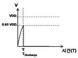
도 2a 내지 도 2c는 본 발명의 개념을 설명하기 위한 도면들이고, 도 3은 도 2a의 점 A에서 측정되는 충전시간(T)에 따른 충전전압(V) 그래프이다.2A to 2C are diagrams for explaining the concept of the present invention, and FIG. 3 is a graph of the charging voltage V according to the charging time T measured at point A of FIG. 2A.
먼저, 도 2a를 참조하면, 도 1과 마찬가지로 제1저항막(30a)에 X+ 전극과 X- 전극이 서로 나란하게 설치되며, 제2저항막(20a)에는 상기 X+ 전극 및 X- 전극과는 수직하게 위치하도록 Y+ 전극 및 Y- 전극이 서로 나란하게 설치된다.First, referring to FIG. 2A, similarly to FIG. 1, an X + electrode and an X− electrode are disposed in parallel with each other in the
Y+ 커패시터(CconR)는 한쪽단은 접지되고 다른 한쪽단은 상기 Y+ 전극에 연결되며, Y+ 커패시터(CconR)와 상기 Y+ 전극 사이에는 Y+ 동일 저항선 스위치(SR)가 설치된다. Y- 커패시터(CconL)는 한쪽단은 접지되고 다른 한쪽단은 상기 Y- 전극에 연결되며, Y- 커패시터(CconL)와 상기 Y- 전극 사이에는 Y- 동일 저항선 스위치(SL)가 설치된다.One end of the Y + capacitor CconR is grounded and the other end thereof is connected to the Y + electrode, and a Y + equal resistance switch SR is installed between the Y + capacitor CconR and the Y + electrode. One end of the Y-capacitor (CconL ) is grounded and the other end is connected to the Y-electrode, and a Y-same resistance line switch (SL ) is installed between the Y-capacitor (CconL ) and the Y-electrode. do.
상기 X+ 전극에 전압 VDD를 인가하고 Y- 동일 저항선 스위치(SL)는 열고 Y+ 동일 저항선 스위치(SR)는 닫은 상태에서 점 P를 누르면 제1저항막(30a)과 제2저항막(20a)이 점 P에서 서로 접촉하게 되어 제1저항막(30a)과 제2저항막(20a) 사이에 전류가 흐르므로 제1저항막(30a)에는 저항값 Rv가 형성되고 제2저항막(20a)에는 저항값 RY+가 형성된다.Applying a voltage VDD to the X + electrode and pressing the point P while the Y- same resistance switch SL is opened and the Y + -resistance switch switch SR is closed, the
VDD의 인가가 지속되면 Y+ 커패시터(CconR)에 걸리는 전압 즉, 점 A에서 측정되는 충전시간(T)에 따른 충전전압(V)은 도 3과 같으며, 충전시간(T)이 무한대로 가면 점 A에서의 충전 전압(V)은 VDD가 된다. 점 A에서의 충전시간(T)에 따른 충전전압(V)은 Y+ 커패시터 전압검출수단(102)을 통해서 얻는다.When the application of VDD continues, the voltage applied to the Y + capacitor CconR , that is, the charging voltage V according to the charging time T measured at the point A is shown in FIG. 3, and when the charging time T goes to infinity, The charging voltage V at point A becomes VDD. The charging voltage V according to the charging time T at the point A is obtained through the Y + capacitor voltage detecting means 102.
Y+ 커패시터 충전 시정수 측정수단(202)은 Y+ 커패시터 전압검출수단(102)에서 측정되는 전압을 통하여 0.632 x VDD일 때의 시간 즉 Y+ 커패시터(CconR)의 충전 시정수(τ)를 얻는다.The Y + capacitor charge time constant measuring means 202obtains the time at the time of0.632 x VDD, that is, the charge time constant?Of the Y + capacitor CconR , through the voltage measured by the Y + capacitor voltage detecting means 102.
Y+ 동일 저항선 연산수단(302)은 Y+ 커패시터(CconR)의 충전 시정수(τ)가 (Rv + RY+) x CconR 로 주어짐을 이용하여 (Rv + RY+) 값을 구한다. 이 때 (Rv + RY+) 값은 대각선 형태의 동일 저항선(152)을 따라 분포한다. 즉, 점 P1이 터치된 경우의 (Rv + RY+)값과 점 P가 터치된 경우의(Rv + RY+)값이 동일하기 때문에 (Rv + RY+)값에 따른 동일 저항선(152)만 가지고는 터치위치(점P)를 파악할 수 없다.Y + In the same resistance calculating means 302 is Y + capacitor charging time constant (τ) of (CconR) is (Rv + RY +) by using a given by x CconR (Rv + RY +) calculated values. At this time, the value of (Rv + RY + ) is distributed along the
따라서 도 2a에서와 같이 (Rv + RY+)값에 따른 동일 저항선(152) 이외에 도 2b에서와 같이 (Rv + RY-)값에 따른 동일 저항선(151)을 얻는 과정을 거친다. 구체적으로 Y+ 동일 저항선 스위치(SR)를 열고 Y- 동일 저항선 스위치(SL)를 닫는다. 그러면, 도 2a에서 설명한 바와 마찬가지로 Y- 커패시터(CconL)에 걸리는 전압 즉, 점 B에서의 충전시간(T)에 따른 충전전압(V)을 Y- 커패시터 전압검출수단(101)을 통해서 얻을 수 있고, Y- 커패시터 충전시정수 측정수단(201)은 이를 통해 Y- 커패시터(CconL)의 충전 시정수(τ)를 얻는다.Therefore, in addition to the
그러면 Y- 동일 저항선 연산수단(301)은 Y- 커패시터(CconL)의 충전 시정수(τ)가 (Rv + RY-) x CconL 로 주어짐을 이용하여 (Rv + RY-) 값을 구한다. 이 때 (Rv + RY-) 값에 따른 동일 저항선(151)만 가지고는 점 P2가 터치되었는지 점 P가 터치되었는지 구분할 수 없게 된다.The Y- same resistance calculating means 301, the charging time constant (τ) is (Rv + RY-) by using the given inconL x C (Rv + RY-) of the Y- capacitor (CconL) Find the value. At this time, it is not possible to distinguish whether the point P2 is touched or the point P is touched with only the
터치좌표계산수단(400)은 (Rv + RY+) 값에 따른 동일 저항선(152)과 (Rv + RY-) 값에 따른 동일 저항선(151)의 교차점을 찾아 정확한 터치좌표(P)를 파악한다.The touch
한편, 임의의 충전시간(t)에서 Y+ 커패시터(CconR)에의 충전전압을 Vc라 하면,


이 경우 Y+ 커패시터 전압검출수단(102)을 통해서 측정되는 충전전압을 통하여 Y+ 커패시터 충전 시정수 측정수단(202)은 사용자가 원하는 충전레벨(


아래에서 설명의 편의상 충전레벨(
도 4는 도 2c의 변형예를 설명하기 위한 도면이다. Y+ 커패시터(CconR)와 Y- 커패시터(CconL)가 구별되어 설치되는 도 2c의 경우와 달리 공통 커패시터(Ccon)가 설치되는 것이 특징이다.4 is a diagram for explaining a modification of FIG. 2C. Unlike the case of FIG. 2C in which the Y + capacitor CconR and the Y- capacitor CconL are separately installed, the common capacitor Ccon is installed.
공통 커패시터(Ccon)는 한쪽단은 접지되고 다른 한쪽단은 Y+ 전극과 Y- 전극에 연결되며, 공통 커패시터(Ccon)와 Y+ 전극 사이에는 Y+ 동일 저항선 스위치(SR)가 설치되고, 공통 커패시터(Ccon)와 Y- 전극 사이에는 Y- 동일 저항선 스위치(SL)가 설치된다.One end of the common capacitor (Ccon ) is grounded and the other end is connected to the Y + electrode and the Y- electrode, and a Y + equal resistance line switch (SR ) is installed between the common capacitor (Ccon ) and the Y + electrode. Between the capacitor Ccon and the Y-electrode, a Y- same resistance line switch SL is provided.
공통 커패시터 전압검출수단(100)은 X+ 전극에 VDD를 인가하고 상기 Y- 동일 저항선 스위치(SL)는 열고 상기 Y+ 동일 저항선 스위치(SR)는 닫은 상태에서 제1저항막(20a)과 제2저항막(30a)이 터치압력에 의하여 점 P에서 접촉되는 경우 그 접촉점(점 P)을 통하여 제1저항막(20a)과 제2저항막(30a) 사이에 전류가 흐를 때에 공통 커패시터(Ccon)에 걸리는 점 A에서의 전압과, 상기 X+ 전극에 VDD를 인가하고 상기 Y+ 동일 저항선 스위치(SR)는 열고 상기 Y- 동일 저항선 스위치(SL)는 닫은 상태에서 제1저항막(20a)과 제2저항막(30a)이 터치압력에 의하여 점 P에서 서로 접촉되는 경우 그 접촉점(점 P)을 통하여 제1저항막(20a)과 제2저항막(30a) 사이에 전류가 흐를 때에 공통 커패시터(Ccon)에 걸리는 점 A에서의 전압을 측정한다.The common capacitor voltage detecting means 100 applies VDD to the X + electrode, opens the Y− resistance line switch SL , and closes the Y + resistance line switch SR. When the
공통 커패시터 충전시정수 측정수단(200)은 공통 커패시터 전압검출수단(200)에서 측정되는 전압을 통하여 공통 커패시터의 충전 시정수(τ)를 얻는다.The common capacitor charge time constant measuring means 200 obtains the charge time constant τ of the common capacitor through the voltage measured by the common capacitor
동일 저항선 연산수단(300)은 도 2a 및 도 2b에서와 마찬가지로 (Rv + RY+) 값에 따른 동일 저항선과, (Rv + RY-)값에 따른 동일 저항선을 얻고, 터치좌표연산수단(400)은 상기 (Rv + RY+) 값에 따른 동일 저항선과 상기 (Rv + RY-) 값에 따른 동일 저항선의 교차점을 찾아 상기 교차점을 터치좌표(점 P)로 인식한다.The same resistance line calculating means 300 obtains the same resistance line according to the value of (Rv + RY + ) and the same resistance line according to the value of (Rv + RY− ), as in FIGS. 2A and 2B. 400 finds an intersection point of the same resistance line according to the value of (Rv + RY + ) and the same resistance line according to the value of (Rv + RY− ) and recognizes the intersection point as a touch coordinate (point P).
도 5는 도 2a의 점 A에서 측정되는 충방전시간(T)에 따른 충방전전압(V) 그래프이다. 도 5에서 도시된 바와 같이 Y+ 커패시터(CconR)가 Tcharge초 동안 충전된 후 방전되는 데에는 마찬가지로 (Tdischarge-Tcharge)초의 시간의 걸린다. 따라서 터치 시 마다 충전 시정수(τ)를 측정하는데 시간이 요구된다.FIG. 5 is a graph of charge / discharge voltage V according to the charge / discharge time T measured at point A of FIG. 2A. As shown in FIG. 5, it takes a time of (Tdischarge −Tcharge ) seconds todischarge after the Y + capacitor CconR is charged for Tcharge seconds. Therefore, time is required for measuring the charging time constant τ for each touch.
도 6은 도 2c에서 이러한 충전시정수(τ)의 측정시간을 단축시킨 변형예를 설명하기 위한 도면이다. 도 6의 경우에는 2개의 커패시터(CconR, CconL)가 설치되는 도 2c의 경우와 달리 4개의 커패시터(CconR1, CconR2, CconL1, CconL2)가 설치된다.FIG. 6 is a view for explaining a modified example in which the measurement time of the charging time constant τ is shortened in FIG. 2C. In the case of Figure 6 it is provided with two capacitors (CconR, CconL) four capacitors unlike in the case of Figure 2c, which is installed(C conR1, C conR2, C conL1, C conL2).
2개의 Y+ 커패시터(CconR1, CconR2) 각각은 한쪽단은 접지되고 다른 한쪽단은 Y+ 전극에 연결된다. 2개의 Y- 커패시터(CconL1, CconL2) 각각은 한쪽단은 접지되고 다른 한쪽단은 Y- 전극에 연결된다.Each of the two Y + capacitors CconR1 and CconR2 is grounded at one end and connected to the Y + electrode at the other end. Each of the two Y-capacitors CconL1 , CconL2 is grounded at one end and connected to the Y- electrode at the other end.
상기 Y+ 전극과 Y+ 제1커패시터(CconR1)사이에는 Y+ 동일 저항선 제1스위치(SR1)가 설치되고, 상기 Y+ 전극과 Y+ 제2커패시터(CconR2)사이에는 Y+ 동일 저항선 제2스위치(SR2)가 설치된다. 상기 Y- 전극과 Y- 제1커패시터(CconL1)사이에는 Y- 동일 저항선 제1스위치(SL1)가 설치되고, 상기 Y- 전극과 Y- 제2커패시터(CconL2) 사이에는 Y- 동일 저항선 제2스위치(SL2)가 설치된다.Wherein Y + electrode and the Y + the first capacitor (CconR1) between, the Y + In the same resistance wire the first switch, and the installation (SR1), wherein Y + electrode and the Y + the second between the capacitor (CconR2) Y + In the same resistance wire a second switch (SR2 ) is installed. A first switch SL1 having the same resistance wire is installed between the Y- electrode and the Y-first capacitor CconL1 , and Y-same between the Y-electrode and the Y-second capacitor CconL2 . The resistance wire second switch SL2 is installed.
Y+ 동일 저항선 제1스위치(SR1)와 Y+ 동일 저항선 제2스위치(SR2)는 서로 교번하여 열리고 닫히며, Y- 동일 저항선 제1스위치(SL1)와 Y- 동일 저항선 제2스위치(SL2)도 서로 교번하여 열리고 닫힌다.The Y + same resistance line first switch SR1 and the Y + same resistance line second switch SR2 are alternately opened and closed, and the Y- same resistance line first switch SL1 and the Y- same resistance line second switch SL2 ) also alternately opens and closes.
따라서 Y+ 커패시터 전압검출수단(102)은 번갈아 가면서 Y+ 제1커패시터(CconR1)와 Y+ 제2커패시터(CconR2)의 양단에 걸리는 전압 즉, 점 A와 A'에서의 전압을 읽으며, Y- 커패시터 전압검출수단(101)은 번갈아 가면서 Y- 제1커패시터(CconL1)와 Y- 제2커패시터(CconL2)의 양단에 걸리는 전압 즉, 점 B와 B'에서의 전압을 읽는다.Therefore, the Y + capacitor
이와 같이 커패시터에 걸리는 전압을 번갈아 읽음으로써 방전시간(Tdischarge-Tcharge)을 고려하지 않아도 되기 때문에 도 2의 경우에 비하여 최고 2배의 빠른 속도로 충전 시정수(τ)를 구할 수 있게 된다.Thus, since the discharge time (Tdischarge -Tcharge ) does not have to be taken into account by alternately reading the voltage applied to the capacitor, the charging time constant τ can be obtained at a speed up to 2 times faster than in the case of FIG.
도 7은 도 6의 변형예를 설명하기 위한 도면으로서, 도 6의 경우와 달리 2개의 공통 커패시터(Ccon1, Ccon2)가 설치되는 것을 특징으로 한다.FIG. 7 is a view for explaining a modification of FIG. 6, and unlike the case of FIG. 6, two common capacitors Ccon1 and Ccon2 are installed.
이 때, 2개의 공통 커패시터(Ccon1, Ccon2) 각각은 한쪽단은 접지되고 다른 한쪽단은 Y+ 전극과 Y1 전극에 연결된다. 제1공통커패시터(Ccon1)와 상기 Y+ 전극 사이에는 Y+ 동일 저항선 제1스위치(SR1)가 설치되고, 제2공통커패시터(Ccon2)와 상기 Y+ 전극 사이에는 Y+ 동일 저항선 제2스위치(SR2)가 설치된다. 제1공통커패시터(Ccon1)와 상기 Y- 전극 사이에는 Y- 동일 저항선 제1스위치(SL1)가 설치되며, 제2커패시터(Ccon2)와 상기 Y-전극 사이에는 Y- 동일 저항선 제2스위치(SL2)가 설치된다.In this case, each of the two common capacitors Ccon1 and Ccon2 is grounded at one end and connected to the Y + electrode and the Y1 electrode. A first common capacitor (Ccon1) and the Y + between electrodes Y + In the same resistance wire the first switch (SR1) there are installed, between the second common capacitor (Ccon2) and the Y + electrode Y + In the same resistance wire a second switch (SR2 ) is installed. A first switch SL1 of Y- same resistance is installed between the first common capacitor Ccon1 and the Y-electrode, and a second resistance line of Y- same resistance is provided between the second capacitor Ccon2 and the Y-electrode. The switch SL2 is installed.
2개의 커패시터(Ccon1,Ccon2)에 걸리는 전압 즉, 점 A 및 A'에 걸리는 시간에 따른 전압은 공통 커패시터 전압검출수단(100)에 의해 측정된다.The voltage across the two capacitors Ccon1 , Ccon2 , that is, the voltage over time across the points A and A ', is measured by the common capacitor voltage detection means 100.
도 8은 도 2c의 충전시정수(τ)의 측정시간을 단축시킨 다른 변형예를 설명하기 위한 도면이다. 이 경우는 도 2c에 추가로 2개의 전하방전수단(501, 502)과 2개의 방전용 스위치(SDR, SDL)가 설치되는 것을 특징으로 한다.FIG. 8 is a view for explaining another modified example in which the measurement time of the charging time constant τ of FIG. 2C is shortened. In this case, two charge and discharge means 501 and 502 and two discharge switches SDR and SDL are provided in addition to FIG. 2C.
Y+ 스위치(SR)가 닫히면서 점 A에서의 전압을 읽으며, 점 A에서의 전압이 0.632 x VDD에 이를 때, Y+스위치를 열고 방전스위치(SDR)을 닫으면 도 14에 도시한 바와 같이 0.632 x VDD 전압 레벨의 충전시정수(τ)에 곧 바로 방전이 이루어진다. 마찬 가지로 Y- 커패시터(CconL)에 충전되는 전압이 사용자가 원하는 전위에 이를 때 Y- 스위치를 열고 방전 스위치(SDL)을 닫으면 도 14에 도시한 바와 같이 0.632 x VDD 전압 레벨의 충전시정수(τ)에 곧 바로 방전이 이루어진다. 이와 같이 커패시터에 걸리는 전압을 곧바로 방전함으로써 방전시간(Tdischarge-Tcharge)을 고려하지 않아도 되기 때문에 제1실시예의 경우에 비하여 최고 4배의 빠른 속도로 충전 시정수(τ)를 구할 수 있게 된다.When the Y + switch SR is closed and the voltage at point A is read and the voltage at point A reaches 0.632 x VDD, opening the Y + switch and closing the discharge switch SDR 0.632 as shown in FIG. Discharge immediately occurs at the charging time constant τ of the x VDD voltage level. Likewise, when the voltage charged to the Y-capacitor (CconL ) reaches the desired potential, when the Y-switch is opened and the discharge switch (SDL ) is closed, the charging timing of the voltage level of 0.632 x VDD as shown in FIG. Discharge immediately occurs in the number τ. Thus, since the discharge time (Tdischarge -Tcharge ) does not have to be taken into consideration by immediately discharging the voltage applied to the capacitor, the charging time constant τ can be obtained at a speed up to four times faster than in the first embodiment. .
[실시예1]Example 1
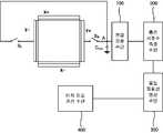
도 9는 본 발명에 따른 다중터치인식 저항막 방식 터치스크린의 기본 구조를 설명하기 위한 도면이다. 구체적으로, 제1투명필름(300)과 제2투명필름(200)은 소정간격 이격되도록 설치되며, 제1투명필름(300)의 아랫면에는 제1저항막(300a)이 설치되고, 제2투명필름(200)의 윗면에는 제2저항막(200a)이 설치된다. 이 때 다중터치인식을 위해서 도 1의 경우와 달리 제1저항막(300a)은 복수개의 제1저항띠가 서로 나란하게 배열되어 이루어지며, 제2저항막(200a)은 상기 제1저항띠와 수직하게 꼬인 위치에 있는 복수개의 제2저항띠를 포함하여 이루어진다.9 is a view for explaining the basic structure of a multi-touch resistive resistive touch screen according to the present invention. Specifically, the first
상기 복수개의 제1저항띠의 양단에는 복수개의 X+ 전극(X1+ ~ Xn+)과 X- 전극(X1- ~Xn-)이 설치된다. 상기 복수개의 제2저항띠의 양단에는 복수개의 Y+ 전극(Y1+ ~ Yn+)과 Y- 전극(Y1- ~Yn-)이 각각 설치된다.A plurality of X + electrodes X1+ to Xn + and X- electrodes X1- to Xn− are provided at both ends of the plurality of first resistance bands. A plurality of Y + electrodes (Y1+ to Yn + ) and Y- electrodes (Y1- to Yn- ) are respectively provided at both ends of the plurality of second resistance bands.
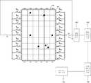
도 10은 본 발명의 제1실시예에 따른 다중터치인식 저항막 방식 터치스크린의 동작원리를 설명하기 위한 도면이다. 구체적으로, 복수개의 Y+ 전극(Y1+ ~ Y9+)에는 복수개의 Y+ 띠선택 스위치(SY1+ ~SY9+)가 일대일 대응하도록 설치되며, 복수개의 Y- 전극(Y1- ~ Y9-)에는 복수개의 Y- 띠선택 스위치(SY1- ~SY9-)가 일대일 대응하도록 설치된다.10 is a view for explaining the operation principle of the multi-touch resistive touch screen according to the first embodiment of the present invention. Specifically, the plurality of Y + electrodes Y1+ to Y9+ are provided with a plurality of Y + band selection switches SY1 + to SY9 + to correspond one-to-one, and the plurality of Y- electrodes Y1- to Y9-. ), A plurality of Y- band select switches SY1 to SY9 -are provided to correspond one-to-one.
Y+ 커패시터(CconR)는 한쪽단은 접지되고 다른 한쪽단과 Y+ 띠선택 스위 치(SY1+ ~SY9+) 사이에는 Y+ 동일 저항선 스위치(SR)가 설치된다. Y- 커패시터(CconL)는 한쪽단은 접지되고 다른 한쪽단과 Y- 띠선택 스위치(SY1- ~SY9-) 사이에는 Y- 동일 저항선 스위치(SL)가 설치된다.One end of the Y + capacitor (CconR ) is grounded, and a Y + equal resistance switch (SR ) is installed between the other end and the Y + band selection switch (SY1 + to SY9 + ). One end of the Y-capacitor CconL is grounded, and a Y-same resistance line switch SL is installed between the other end and the Y-band selection switches SY1 -SY9- .
점 A의 좌표The coordinates of point A
X1+ 전극부터 X6- 전극에는 순차적으로 VDD가 인가되는데, 점 A의 터치좌표가 인식되는 경우는 X2+ 전극에 VDD가 인가될 때이다.VDD is sequentially applied to the X1 + electrodes to the X6-electrodes. When the touch coordinate of point A is recognized, VDD is applied to the X2 + electrode.
SY1+ 띠선택 스위치와 Y+ 동일 저항선 스위치(SR)는 닫고, 나머지 스위치들은 모두 열면 제1저항막에는 저항값 Rv가 형성되고 제2저항막에는 저항값 RY+가 형성된다. 이 때 Y+ 커패시터(CconR)의 충전시간(T)에 따른 충전전압(V)은 Y+ 커패시터 전압검출수단(102)을 통해서 얻는다.When the SY1 + band selection switch and the Y + same resistance line switch SR are closed and the remaining switches are opened, a resistance value Rv is formed in the first resistance film and a resistance value RY + is formed in the second resistance film. At this time, the charging voltage V according to the charging time T of the Y + capacitor CconR is obtained through the Y + capacitor
Y+ 커패시터 충전 시정수 측정수단(202)은 Y+ 커패시터 전압검출수단(102)에서 측정되는 전압을 통하여 0.632 x VDD일 때의 시간 즉 Y+ 커패시터(CconR)의 충전 시정수(τ)를 얻는다.The Y + capacitor charge time constant measuring means 202obtains the time at the time of0.632 x VDD, that is, the charge time constant?Of the Y + capacitor CconR , through the voltage measured by the Y + capacitor
Y+ 동일 저항선 연산수단(302)은 Y+ 커패시터(CconR)의 충전 시정수(τ)가 (Rv + RY+) x CconR 로 주어짐을 이용하여 (Rv + RY+) 값을 구한다.Y + In the same resistance calculating means 302 is Y + capacitor charging time constant (τ) of (CconR) is (Rv + RY +) by using a given by x CconR (Rv + RY +) calculated values.
SY1- 띠선택 스위치와 Y- 동일 저항선 스위치(SL)는 닫고, 나머지 스위치들 은 모두 열면 제1저항막에는 저항값 Rv가 형성되고 제2저항막에는 저항값 RY-가 형성된다. 이 때 Y- 커패시터(CconL)의 충전시간(T)에 따른 충전전압(V)은 Y- 커패시터 전압검출수단(101)을 통해서 얻는다. Y- 커패시터 충전시정수 측정수단(201)은 이를 통해 Y- 커패시터(CconL)의 충전 시정수(τ)를 얻는다. 그러면 Y- 동일 저항선 연산수단(301)은 Y- 커패시터(CconL)의 충전 시정수(τ)가 (Rv + RY-) x CconL 로 주어짐을 이용하여 (Rv + RY-) 값을 구한다.When the SY1- band select switch and the Y- same resistance line switch SL are closed and all other switches are opened, a resistance value Rv is formed in the first resistance film and a resistance value RY- is formed in the second resistance film. . At this time, the charging voltage V according to the charging time T of the Y-capacitor CconL is obtained through the Y-capacitor
터치좌표계산수단(400)은 (Rv + RY+) 값에 따른 동일 저항선과 (Rv + RY-) 값에 따른 동일 저항선의 교차점을 찾아 정확한 터치좌표(A)를 파악한다.The touch coordinate calculating
점 B의 좌표The coordinates of point B
X4+ 전극에 VDD를 인가하고, SY1+ 띠선택 스위치와 Y+ 동일 저항선 스위치(SR)는 닫고 나머지 스위치들은 모두 열고, 다음에 SY1- 띠선택 스위치와 Y- 동일 저항선 스위치(SL)는 닫고 나머지 스위치들은 모두 열어서 상기 점 A의 좌표인식과 동일한 방법으로 점 B의 터치좌표를 구할 수 있다.Apply VDD to the X4 + electrode, close the SY1 + band select switch and the Y + equal resistance switch (SR ), open all other switches, then close the SY1- band select switch and the Y- equal resistance switch (SL ), All other switches can be opened to obtain the touch coordinates of the point B in the same manner as the coordinate recognition of the point A.
다만, B의 좌표가 인근셀에도 걸쳐져 있으므로 나머지 3개의 셀 즉, (X4, Y2), (X5, Y1), (X5, Y2)에 대해서도 동일한 방법으로 좌표를 측정하고 그 평균값을 가지고 정확히 점 B의 좌표를 계산하는 과정을 거친다.However, since the coordinates of B span the neighboring cells, the coordinates are measured in the same manner for the remaining three cells, that is, (X4, Y2), (X5, Y1), and (X5, Y2). Calculate the coordinates of
점 C의 좌표The coordinates of point C
특히 점 C의 경우에는 일반적인 매트릭스 방법으로는 점 A 와 점 D를 터치한 상태에서 점 C를 터치하게 되면 감지가 되지 않으나 본 발명과 같은 방식에서는 이와 같은 경우에도 점 C도 독립적으로 감지된다.Particularly, in the case of point C, when the point C is touched while the point A and the point D are touched by the general matrix method, the point C is not detected in the same manner as in the present invention.
[실시예2]Example 2
도 11은 본 발명의 제2실시예에 따른 다중터치인식 저항막 방식 터치스크린을 설명하기 위한 도면이다. 도 4의 경우와 마찬가지로 Y+ 전극과 Y-전극에 공통 커패시터(Ccon)가 설치되는 것이 특징이다.11 is a view for explaining a multi-touch resistive touch screen according to a second embodiment of the present invention. As in the case of FIG. 4, the common capacitor Ccon is installed on the Y + electrode and the Y-electrode.
[실시예3]Example 3
도 12는 본 발명의 제3실시예에 따른 다중터치인식 저항막 방식 터치스크린을 설명하기 위한 도면이다. 도 6에서 설명한 바와 같이 Y+ 커패시터(CconR1, CconR2)와 Y- 커패시터(CconL1, CconL2R)를 복수개 설치하여 이들을 교대로 동작시킴으로서 방전시간에 따른 지연을 최소화하는 것을 특징으로 한다.12 is a view for explaining a multi-touch resistive touch screen according to a third embodiment of the present invention. As described in FIG. 6, aplurality of Y + capacitors CconR1 and CconR2 and a plurality of Y-capacitors CconL1 and CconL2R are installed and operated alternately to minimize delay due to discharge time.
[실시예4]Example 4
도 13은 본 발명의 제4실시예에 따른 다중터치인식 저항막 방식 터치스크린을 설명하기 위한 도면으로서, 제1실시예에 추가로 2개의 전하방전수단(501, 502)과 2개의 방전용 스위치(SDR, SDL)가 설치되는 것을 특징으로 한다.FIG. 13 is a view for explaining a multi-touch resistive touch screen according to a fourth embodiment of the present invention. In addition to the first embodiment, two charge and discharge means 501 and 502 and two discharge switches are shown. (SDR , SDL ) is characterized in that is installed.
Y+ 스위치(SR)가 닫히면서 점 A에서의 전압을 읽으며, 점 A에서의 전압이 0.632 x VDD에 이를 때, Y+스위치를 열고 방전스위치(SDR)을 닫으면 곧 바로 방전이 이루어진다. 마찬 가지로 Y- 커패시터(CconL)에 충전되는 전압이 사용자가 원하는 전위에 이를 때 Y- 스위치를 열고 방전 스위치(SDL)을 닫으면 도 14에 도시한 바와 같이 0.632*VDD 전압 레벨의 충전시정수(τ)에 곧바로 방전이 이루어진다. 이와 같이 커패시터에 걸리는 전압을 곧바로 방전함으로써 방전시간(Tdischarge-Tcharge)을 고려하지 않아도 되기 때문에 제1실시예의 경우에 비하여 최고 4배의 빠른 속도로 충전 시정수(τ)를 구할 수 있게 된다.The voltage at point A is read as the Y + switch SR closes, and when the voltage at point A reaches 0.632 x VDD, the discharge occurs immediately after opening the Y + switch and closing the discharge switch SDR . Likewise, when the voltage charged to the Y-capacitor (CconL ) reaches the desired potential, when the Y-switch is opened and the discharge switch (SDL ) is closed, the charging time of 0.632 * VDD voltage level is as shown in FIG. Discharge immediately occurs in the number τ. Thus, since the discharge time (Tdischarge -Tcharge ) does not have to be taken into consideration by immediately discharging the voltage applied to the capacitor, the charging time constant τ can be obtained at a speed up to four times faster than in the first embodiment. .
본 발명에 의하면, 커패시터 충전 시정수를 통하여 터치위치를 파악하기 때문에 종래와 같은 ADC(analog to digital convertor)를 사용하지 않을 수 있어 IC 집적화에 유리하다. 이 때 커패시터를 복수개 설치하여 번갈아 동작시키거나 전하 방전장치를 이용하여 캐패시터 내부에 충전된 전하를 강제 방전하면 방전시간에 따른 시간 지연을 최소화 시킬 수 있다. 그리고 저항막이 하나의 면 형태가 아닌 여러개의 띠(stripe)로 분리되게 설치되므로 다중터치인식이 가능할 뿐만 아니라 면저항에 의해 터치위치의 감지오차가 발생하는 것을 방지할 수 있다.According to the present invention, since the touch position is determined through the capacitor charging time constant, an analog to digital converter (ADC) may not be used, which is advantageous for IC integration. At this time, by installing a plurality of capacitors to operate alternately or by forcibly discharging the charge charged in the capacitor using a charge discharge device it can minimize the time delay according to the discharge time. In addition, since the resistive film is installed to be separated into multiple strips rather than one surface, not only multi-touch recognition is possible, but also a touch resistance can be prevented from occurring due to sheet resistance.
도 1은 종래의 저항막 방식 터치스크린을 설명하기 위한 도면;1 is a view for explaining a conventional resistive touch screen;
도 2a 내지 도 2c는 본 발명의 개념을 설명하기 위한 도면들;2a to 2c are views for explaining the concept of the present invention;
도 3은 도 2a의 점 A에서 측정되는 충전시간(T)에 따른 충전전압(V) 그래프;3 is a graph of charging voltage (V) according to the charging time (T) measured at point A of FIG. 2A;
도 4는 도 2c의 변형예를 설명하기 위한 도면;4 is a view for explaining a modification of FIG. 2C;
도 5는 도 2a의 점 A에서 측정되는 충방전시간(T)에 따른 충방전전압(V) 그래프;5 is a graph of charge and discharge voltage (V) according to the charge and discharge time (T) measured at point A of FIG. 2A;
도 6은 도 2c에서 충전시정수(τ)의 측정시간을 단축시킨 변형예를 설명하기 위한 도면;FIG. 6 is a view for explaining a modified example in which the measurement time of the charging time constant? Is shortened in FIG. 2C;
도 7은 도 6의 변형예를 설명하기 위한 도면;7 is a view for explaining a modification of FIG. 6;
도 8은 도 2c에서 충전시정수(τ)의 측정시간을 단축시킨 다른 변형예를 설명하기 위한 도면;8 is a view for explaining another modified example in which the measurement time of the charging time constant? Is shortened in FIG. 2C;
도 9는 본 발명에 따른 다중터치인식 저항막 방식 터치스크린의 기본 구조를 설명하기 위한 도면;9 is a view for explaining the basic structure of a multi-touch resistive resistive touch screen according to the present invention;
도 10은 본 발명의 제1실시예에 따른 다중터치인식 저항막 방식 터치스크린의 동작원리를 설명하기 위한 도면;10 is a view for explaining the operation principle of a multi-touch resistive touch screen according to a first embodiment of the present invention;
도 11은 본 발명의 제2실시예에 따른 다중터치인식 저항막 방식 터치스크린을 설명하기 위한 도면;11 is a view for explaining a multi-touch resistive touch screen according to a second embodiment of the present invention;
도 12는 본 발명의 제3실시예에 따른 다중터치인식 저항막 방식 터치스크린을 설명하기 위한 도면;12 is a view for explaining a multi-touch resistive touch screen according to a third embodiment of the present invention;
도 13은 본 발명의 제4실시예에 따른 다중터치인식 저항막 방식 터치스크린을 설명하기 위한 도면;13 is a view for explaining a multi-touch resistive touch screen according to a fourth embodiment of the present invention;
도 14는 본 발명의 실시예의 일부에 적용된 강제 방전에 대한 전압 그래프이다.14 is a voltage graph for forced discharge applied to some of the embodiments of the present invention.
<도면의 주요부분에 대한 참조번호의 설명><Description of reference numbers for the main parts of the drawings>
20, 200: 제2투명필름20, 200: second transparent film
20a, 200a: 제2저항막20a, 200a: second resistive film
30, 300: 제1투명필름30, 300: first transparent film
30a, 300a: 제1저항막30a, 300a: first resistive film
101: Y- 커패시터 전압검출수단101: Y-capacitor voltage detection means
102: Y+ 커패시터 전압검출수단102: Y + capacitor voltage detection means
201: Y- 커패시터 충전 시정수 측정수단201: Y-capacitor charge time constant measuring means
202: Y+ 커패시터 충전 시정수 측정수단202: Y + capacitor charge time constant measuring means
301: Y- 동일 저항선 연산수단301: Y-I resistance line calculating means
302: Y+ 동일 저항선 연산수단302: Y + equal resistance line calculating means
151: (Rv + RY-)값에 따른 동일 저항선151: Same resistance wire according to (Rv + RY- )
152: (Rv + RY+)값에 따른 동일 저항선152: Same resistance wire according to (Rv + RY + )
400: 터치좌표계산수단400: touch coordinate calculation means
Claims (7)
Translated fromKorean


Priority Applications (4)
| Application Number | Priority Date | Filing Date | Title |
|---|---|---|---|
| KR1020090035025AKR100933037B1 (en) | 2009-04-22 | 2009-04-22 | Multi-Touch Resistive Touch Screen Recognizing Multi-Touch Coordinates Through Capacitor Charging Time |
| US13/265,364US8711123B2 (en) | 2009-04-22 | 2010-01-14 | Multi-touch recognition resistive touch screen for recognizing multi-touch coordinates through capacitor charging time |
| CN2010800219165ACN102439546A (en) | 2009-04-22 | 2010-01-14 | Multi-touch recognition resistive touch screen for recognizing multi-touch coordinates through capacitor charging time |
| PCT/KR2010/000219WO2010123191A1 (en) | 2009-04-22 | 2010-01-14 | Multi-touch recognition resistive touch screen for recognizing multi-touch coordinates through capacitor charging time |
Applications Claiming Priority (1)
| Application Number | Priority Date | Filing Date | Title |
|---|---|---|---|
| KR1020090035025AKR100933037B1 (en) | 2009-04-22 | 2009-04-22 | Multi-Touch Resistive Touch Screen Recognizing Multi-Touch Coordinates Through Capacitor Charging Time |
Publications (1)
| Publication Number | Publication Date |
|---|---|
| KR100933037B1true KR100933037B1 (en) | 2009-12-21 |
Family
ID=41684513
Family Applications (1)
| Application Number | Title | Priority Date | Filing Date |
|---|---|---|---|
| KR1020090035025AExpired - Fee RelatedKR100933037B1 (en) | 2009-04-22 | 2009-04-22 | Multi-Touch Resistive Touch Screen Recognizing Multi-Touch Coordinates Through Capacitor Charging Time |
Country Status (4)
| Country | Link |
|---|---|
| US (1) | US8711123B2 (en) |
| KR (1) | KR100933037B1 (en) |
| CN (1) | CN102439546A (en) |
| WO (1) | WO2010123191A1 (en) |
Families Citing this family (3)
| Publication number | Priority date | Publication date | Assignee | Title |
|---|---|---|---|---|
| TWI400646B (en) | 2009-08-12 | 2013-07-01 | Htc Corp | Method for detecting pressure of touch sensing element and electronic device using the same |
| KR101934310B1 (en)* | 2012-08-24 | 2019-01-03 | 삼성디스플레이 주식회사 | touch display apparatus sensing touch force |
| CN115932643B (en)* | 2022-11-14 | 2025-06-06 | 珠海市宏沛函电子技术有限公司 | Capacitive touch screen short circuit testing method, device, touch screen and equipment |
Citations (2)
| Publication number | Priority date | Publication date | Assignee | Title |
|---|---|---|---|---|
| KR970028977A (en)* | 1995-11-13 | 1997-06-26 | 베일리 웨인 피 | Touch sensitive flat panel display |
| KR20090003137A (en)* | 2008-12-15 | 2009-01-09 | 주식회사 애트랩 | Input device having a resistive touch panel and method for calculating contact position thereof |
Family Cites Families (5)
| Publication number | Priority date | Publication date | Assignee | Title |
|---|---|---|---|---|
| JPH0521148Y2 (en)* | 1988-02-24 | 1993-05-31 | ||
| JP3379276B2 (en)* | 1995-04-24 | 2003-02-24 | 松下電器産業株式会社 | Coordinate position input device |
| JP3221368B2 (en)* | 1997-09-17 | 2001-10-22 | 日本電気株式会社 | Resistive tablet, control method therefor, and recording medium storing program for realizing the method |
| JP3869099B2 (en)* | 1997-11-25 | 2007-01-17 | 株式会社リコー | Touch panel coordinate measuring device |
| US8547114B2 (en)* | 2006-11-14 | 2013-10-01 | Cypress Semiconductor Corporation | Capacitance to code converter with sigma-delta modulator |
- 2009
- 2009-04-22KRKR1020090035025Apatent/KR100933037B1/ennot_activeExpired - Fee Related
- 2010
- 2010-01-14WOPCT/KR2010/000219patent/WO2010123191A1/enactiveApplication Filing
- 2010-01-14USUS13/265,364patent/US8711123B2/enactiveActive
- 2010-01-14CNCN2010800219165Apatent/CN102439546A/enactivePending
Patent Citations (2)
| Publication number | Priority date | Publication date | Assignee | Title |
|---|---|---|---|---|
| KR970028977A (en)* | 1995-11-13 | 1997-06-26 | 베일리 웨인 피 | Touch sensitive flat panel display |
| KR20090003137A (en)* | 2008-12-15 | 2009-01-09 | 주식회사 애트랩 | Input device having a resistive touch panel and method for calculating contact position thereof |
Also Published As
| Publication number | Publication date |
|---|---|
| US20120092291A1 (en) | 2012-04-19 |
| US8711123B2 (en) | 2014-04-29 |
| WO2010123191A1 (en) | 2010-10-28 |
| CN102439546A (en) | 2012-05-02 |
Similar Documents
| Publication | Publication Date | Title |
|---|---|---|
| US8860686B2 (en) | Multi-chip touch screens | |
| KR101076236B1 (en) | Capacitance type touch panel | |
| EP2223200B1 (en) | Pointing and data entry input device | |
| US10754457B2 (en) | Touch-screen panel with multiple sense units and related methods | |
| US8248383B2 (en) | Multi-touch touch screen with single-layer ITO bars arranged in parallel | |
| US8873743B1 (en) | Tapered capsense structure | |
| US7924029B2 (en) | Half-bridge for capacitive sensing | |
| US9152287B2 (en) | System and method for dual-touch gesture classification in resistive touch screens | |
| EP2287716B1 (en) | Method for detecting a position of a touch on touch sensing element and electronic device using the same | |
| US20080088595A1 (en) | Interconnected two-substrate layer touchpad capacitive sensing device | |
| TW201044241A (en) | Two-dimensional position sensor | |
| US8547117B2 (en) | Capacitive touch panel | |
| EP2687961B1 (en) | Input device | |
| CN103365507B (en) | Sensing device and method for improving reliability of capacitive touch device | |
| KR100933037B1 (en) | Multi-Touch Resistive Touch Screen Recognizing Multi-Touch Coordinates Through Capacitor Charging Time | |
| KR101438454B1 (en) | Single layer capacitive type touch screen apparatus capable of multi touch | |
| CN201765576U (en) | Piezoelectric type touch detection system | |
| JP5616923B2 (en) | Input device and position determination method | |
| US20150084924A1 (en) | Position determination techniques in resistive touch screen applications | |
| US9261547B2 (en) | Electrostatic capacitance detection device | |
| KR101032021B1 (en) | Resistive touch screen recognizes touch coordinates through capacitor charging time | |
| KR101671835B1 (en) | Apparatus and method for non-touch testing touch screen module | |
| JP6182031B2 (en) | Capacitance measurement device, capacitance-type surface sensor device, and capacitance-type liquid level detection device | |
| CN108700974B (en) | Capacitance detection circuit and electronic device | |
| WO2008093914A1 (en) | Touch location detecting apparatus for a display screen |
Legal Events
| Date | Code | Title | Description |
|---|---|---|---|
| A201 | Request for examination | ||
| PA0109 | Patent application | St.27 status event code:A-0-1-A10-A12-nap-PA0109 | |
| PA0201 | Request for examination | St.27 status event code:A-1-2-D10-D11-exm-PA0201 | |
| A302 | Request for accelerated examination | ||
| PA0302 | Request for accelerated examination | St.27 status event code:A-1-2-D10-D17-exm-PA0302 St.27 status event code:A-1-2-D10-D16-exm-PA0302 | |
| D13-X000 | Search requested | St.27 status event code:A-1-2-D10-D13-srh-X000 | |
| D14-X000 | Search report completed | St.27 status event code:A-1-2-D10-D14-srh-X000 | |
| E902 | Notification of reason for refusal | ||
| PE0902 | Notice of grounds for rejection | St.27 status event code:A-1-2-D10-D21-exm-PE0902 | |
| P11-X000 | Amendment of application requested | St.27 status event code:A-2-2-P10-P11-nap-X000 | |
| P13-X000 | Application amended | St.27 status event code:A-2-2-P10-P13-nap-X000 | |
| R18-X000 | Changes to party contact information recorded | St.27 status event code:A-3-3-R10-R18-oth-X000 | |
| T11-X000 | Administrative time limit extension requested | St.27 status event code:U-3-3-T10-T11-oth-X000 | |
| E701 | Decision to grant or registration of patent right | ||
| PE0701 | Decision of registration | St.27 status event code:A-1-2-D10-D22-exm-PE0701 | |
| GRNT | Written decision to grant | ||
| PR0701 | Registration of establishment | St.27 status event code:A-2-4-F10-F11-exm-PR0701 | |
| PR1002 | Payment of registration fee | St.27 status event code:A-2-2-U10-U11-oth-PR1002 Fee payment year number:1 | |
| PG1601 | Publication of registration | St.27 status event code:A-4-4-Q10-Q13-nap-PG1601 | |
| FPAY | Annual fee payment | Payment date:20121126 Year of fee payment:4 | |
| PR1001 | Payment of annual fee | St.27 status event code:A-4-4-U10-U11-oth-PR1001 Fee payment year number:4 | |
| FPAY | Annual fee payment | Payment date:20131212 Year of fee payment:5 | |
| PR1001 | Payment of annual fee | St.27 status event code:A-4-4-U10-U11-oth-PR1001 Fee payment year number:5 | |
| FPAY | Annual fee payment | Payment date:20141202 Year of fee payment:6 | |
| PR1001 | Payment of annual fee | St.27 status event code:A-4-4-U10-U11-oth-PR1001 Fee payment year number:6 | |
| LAPS | Lapse due to unpaid annual fee | ||
| PC1903 | Unpaid annual fee | St.27 status event code:A-4-4-U10-U13-oth-PC1903 Not in force date:20151212 Payment event data comment text:Termination Category : DEFAULT_OF_REGISTRATION_FEE | |
| PC1903 | Unpaid annual fee | St.27 status event code:N-4-6-H10-H13-oth-PC1903 Ip right cessation event data comment text:Termination Category : DEFAULT_OF_REGISTRATION_FEE Not in force date:20151212 | |
| P22-X000 | Classification modified | St.27 status event code:A-4-4-P10-P22-nap-X000 |