KR100932892B1 - Multiple removable nonvolatile memory cards in serial communication with the host - Google Patents
Multiple removable nonvolatile memory cards in serial communication with the hostDownload PDFInfo
- Publication number
- KR100932892B1 KR100932892B1KR1020037002335AKR20037002335AKR100932892B1KR 100932892 B1KR100932892 B1KR 100932892B1KR 1020037002335 AKR1020037002335 AKR 1020037002335AKR 20037002335 AKR20037002335 AKR 20037002335AKR 100932892 B1KR100932892 B1KR 100932892B1
- Authority
- KR
- South Korea
- Prior art keywords
- data
- memory
- card
- contacts
- host
- Prior art date
- Legal status (The legal status is an assumption and is not a legal conclusion. Google has not performed a legal analysis and makes no representation as to the accuracy of the status listed.)
- Expired - Fee Related
Links
Images


Classifications
- G—PHYSICS
- G06—COMPUTING OR CALCULATING; COUNTING
- G06F—ELECTRIC DIGITAL DATA PROCESSING
- G06F13/00—Interconnection of, or transfer of information or other signals between, memories, input/output devices or central processing units
- G—PHYSICS
- G06—COMPUTING OR CALCULATING; COUNTING
- G06F—ELECTRIC DIGITAL DATA PROCESSING
- G06F13/00—Interconnection of, or transfer of information or other signals between, memories, input/output devices or central processing units
- G06F13/14—Handling requests for interconnection or transfer
- G06F13/16—Handling requests for interconnection or transfer for access to memory bus
- G06F13/1668—Details of memory controller
- G06F13/1694—Configuration of memory controller to different memory types
- G—PHYSICS
- G06—COMPUTING OR CALCULATING; COUNTING
- G06F—ELECTRIC DIGITAL DATA PROCESSING
- G06F12/00—Accessing, addressing or allocating within memory systems or architectures
- G06F12/02—Addressing or allocation; Relocation
- G06F12/06—Addressing a physical block of locations, e.g. base addressing, module addressing, memory dedication
- G06F12/0646—Configuration or reconfiguration
- G06F12/0653—Configuration or reconfiguration with centralised address assignment
- G06F12/0661—Configuration or reconfiguration with centralised address assignment and decentralised selection
- G—PHYSICS
- G06—COMPUTING OR CALCULATING; COUNTING
- G06F—ELECTRIC DIGITAL DATA PROCESSING
- G06F13/00—Interconnection of, or transfer of information or other signals between, memories, input/output devices or central processing units
- G06F13/38—Information transfer, e.g. on bus
- G06F13/382—Information transfer, e.g. on bus using universal interface adapter
- G06F13/385—Information transfer, e.g. on bus using universal interface adapter for adaptation of a particular data processing system to different peripheral devices
- G—PHYSICS
- G06—COMPUTING OR CALCULATING; COUNTING
- G06F—ELECTRIC DIGITAL DATA PROCESSING
- G06F13/00—Interconnection of, or transfer of information or other signals between, memories, input/output devices or central processing units
- G06F13/38—Information transfer, e.g. on bus
- G06F13/382—Information transfer, e.g. on bus using universal interface adapter
- G06F13/387—Information transfer, e.g. on bus using universal interface adapter for adaptation of different data processing systems to different peripheral devices, e.g. protocol converters for incompatible systems, open system
- G—PHYSICS
- G06—COMPUTING OR CALCULATING; COUNTING
- G06F—ELECTRIC DIGITAL DATA PROCESSING
- G06F13/00—Interconnection of, or transfer of information or other signals between, memories, input/output devices or central processing units
- G06F13/38—Information transfer, e.g. on bus
- G06F13/42—Bus transfer protocol, e.g. handshake; Synchronisation
- G06F13/4204—Bus transfer protocol, e.g. handshake; Synchronisation on a parallel bus
- G06F13/4234—Bus transfer protocol, e.g. handshake; Synchronisation on a parallel bus being a memory bus
- G06F13/4239—Bus transfer protocol, e.g. handshake; Synchronisation on a parallel bus being a memory bus with asynchronous protocol
- G—PHYSICS
- G06—COMPUTING OR CALCULATING; COUNTING
- G06F—ELECTRIC DIGITAL DATA PROCESSING
- G06F2212/00—Indexing scheme relating to accessing, addressing or allocation within memory systems or architectures
- G06F2212/20—Employing a main memory using a specific memory technology
- G06F2212/202—Non-volatile memory
- G06F2212/2022—Flash memory
- G—PHYSICS
- G06—COMPUTING OR CALCULATING; COUNTING
- G06F—ELECTRIC DIGITAL DATA PROCESSING
- G06F2213/00—Indexing scheme relating to interconnection of, or transfer of information or other signals between, memories, input/output devices or central processing units
- G06F2213/0052—Assignment of addresses or identifiers to the modules of a bus system
Landscapes
- Engineering & Computer Science (AREA)
- Theoretical Computer Science (AREA)
- Physics & Mathematics (AREA)
- General Engineering & Computer Science (AREA)
- General Physics & Mathematics (AREA)
- Techniques For Improving Reliability Of Storages (AREA)
- Credit Cards Or The Like (AREA)
- Information Transfer Systems (AREA)
- Fire Alarms (AREA)
- Debugging And Monitoring (AREA)
- Coupling Device And Connection With Printed Circuit (AREA)
- Stored Programmes (AREA)
- Read Only Memory (AREA)
Abstract
Translated fromKoreanDescription
Translated fromKorean본 발명은 전자회로 카드 및 이것을 호스트 장치에 유선으로 연결된 하나 또는 그 이상의 카드 소켓을 구비한 시스템에 이용하는 것에 관한 것으로, 특히 플래시 EEPROM(전기적 소거가능 및 프로그래밍가능 판독 전용 메모리)와 같은 재기록가능 비휘발성 메모리를 상당수 내장하고 있는 소형 캡슐형 카드 및 이 카드가 다중 카드 소켓에 착탈식으로 삽입될 때에 동작하는 시스템에 관한 것이다.The present invention relates to the use of an electronic circuit card and a system having one or more card sockets wired to a host device, in particular rewritable nonvolatile, such as flash EEPROM (electrically erasable and programmable read only memory). A small encapsulated card with a large amount of memory and a system operating when the card is inserted into and detached from a multiple card socket.
개인용 컴퓨터, 노트북 컴퓨터, 개인 전자 단말기, 셀룰러 전화, 카메라, 기타 착탈식 데이터 저장장치가 필요한 전자 장치로부터 배수의(multiple) 메가바이트의 데이터를 저장할 수 있는 비휘발성 반도체 플래시 EEPROM 시스템을 내장하는 소형 카드가 널리 보급되어 왔다. 그와 같은 메모리 카드의 응용은 급속히 증가하고 있으며, 현재는 인터넷으로부터 다운로드된 음악을 저장하는데도 이용되고 있다. 음악 데이터는 통상적으로 잘 알려져 있는 MP-3 알고리즘에 의한 것과 같은 압축형태로 인터넷 상에서 전송되고, 카드에 압축형태로 저장되어 나중에 아날로그 구동 장치에서 압축해제되어 재생된다. 메모리 카드 슬롯(소켓)을 구비한 초소형 바테리 구동 휴대형 플레이어가 널리 보급되기 시작하고 있다. 장래에는 인터넷의 대역폭과 그에 대한 접속이 늘어가고 메모리 카드의 저장 용량이 증가하고 또 데이터 압축 알고리즘의 효율이 증가함에 따라, 그와 같은 카드를 이용하여 비디오나 기타 고용량의 데이터를 저장하고 전송하게 될 것이다.A small card with a non-volatile semiconductor flash EEPROM system that can store multiple megabytes of data from personal computers, notebook computers, personal electronic terminals, cellular phones, cameras, and other electronic devices requiring removable data storage. It has been widely spread. Applications of such memory cards are increasing rapidly, and are currently used to store music downloaded from the Internet. Music data is typically transmitted over the Internet in a compressed form, such as by the well-known MP-3 algorithm, stored in a compressed form on a card and later decompressed and played back in an analog drive. Micro-battery-driven portable players with memory card slots (sockets) are becoming widespread. In the future, as the bandwidth and access to the Internet increases, the storage capacity of memory cards increases, and the efficiency of data compression algorithms increases, such cards will be used to store and transmit video and other high-capacity data. will be.
이들 및 기타 다른 응용에 특별히 적합한 카드는 길이 32 밀리미터, 폭 24 밀리미터, 두께 1.4 밀리미터인 멀티미디어카드("MMC")이다. MMC의 물리적 및 전기적 사양은 캘리포니아주 쿠퍼티노 소재의 멀티미디어카드 협회("MMCA")에 의해 부정기적으로 갱신되고 발간되는 "멀티미디어카드 시스템 사양"에 나타나 있다. 이 사양의 각각 1999년 6월 및 2000년 1월자 2.11 및 2.2판은 본 명세서에 인용으로 포함된다. 하나의 카드에 64 메가바이트까지의 다양한 저장 용량을 가진 MMC 제품은 현재 본 출원의 양수인인 캘리포니아주 서니베일 소재의 샌디스크(SanDisk Corporation)로부터 입수가능하다. 이 제품은 샌디스크에서 2000년 4월에 발간한 "멀티미디어카드 제품 매뉴얼"에 설명되어 있으며, 이 매뉴얼은 본 명세서에 인용으로 포함된다. MMC 제품의 전기적 동작의 특정 양상은 Thomas N. Toombs와 Micky Holtzman의 현재 출원계속 중인 출원번호 제09/185,649호 및 제09/186,064호(모두 1998년 11월 4일자로 출원되었으며, 샌디스크에 양도되어 있음)에도 기술되어 있다. 물리적 카드 구조 및 그 제조 방법은 샌디스크에 양도된 미국특허 제6,040,622호에 기술되어 있다. 이들 출원 및 특허들도 본 명세서에 인용으로 포함된다.Particularly suitable cards for these and other applications are multimedia cards ("MMC") that are 32 millimeters long, 24 millimeters wide, and 1.4 millimeters thick. MMC's physical and electrical specifications are presented in the "Multimedia Card System Specification," which is updated and published irregularly by the Multimedia Card Association ("MMCA") of Cupertino, California. The 2.11 and 2.2 editions of June 1999 and January 2000, respectively, of this specification are incorporated herein by reference. MMC products with varying storage capacities of up to 64 megabytes on one card are available from SanDisk Corporation of Sunnyvale, California, which is the assignee of the present application. This product is described in SanDisk's "Multimedia Card Product Manual" published in April 2000, which is incorporated herein by reference. Certain aspects of the electrical operation of MMC products are currently pending applications Nos. 09 / 185,649 and 09 / 186,064 (both filed Nov. 4, 1998, assigned by Thomas N. Toombs and Micky Holtzman). It is also described in the above). The physical card structure and its manufacturing method are described in US Pat. No. 6,040,622 assigned to SanDisk. These applications and patents are also incorporated herein by reference.
MMC 제품은 데이터 전송용으로 하나, 명령 수신 및 응답(상태 표시) 송신용으로 하나, 클록 신호 수신용으로 하나, 그리고 전력 수신용으로 3개 해서 모두 6개의 전기 접촉부만을 이용하는 직렬 인터페이스를 갖고 있다. 그리고 장래 이용을 위해 여분의 접촉부가 추가되어 있다. 이와 같이 몇 개 안 되는 접촉부는 호스트 시스템 특히, 휴대형의 경우에 카드를 이용하는 것을 간단하게 하며 카드 크기를 줄일 수 있도록 한다. 물론, 다른 포맷을 가진 다른 더 큰 메모리 카드에서처럼 다중 접촉부를 통해 데이터를 병렬로 전송하는 경우와는 달리, 하나의 데이터 접촉부를 이용하는 경우에는 주어진 클록 주파수에 대해서 카드 안팎으로 데이터가 전송될 수 있는 속도가 제한된다. 호스트 시스템은 종종 두 개 또는 그 이상의 MMC 제품의 동시 이용을 위해서 두 개 또는 그 이상의 소켓을 제공한다. 다중 삽입 메모리 카드의 모든 데이터 접촉부는 하나의 라인에 의해 호스트 프로세서에 연결되며, 마찬가지로 모든 명령/응답 접촉부도 하나의 라인에 의해 호스트 프로세서에 연결되며, 카드의 모든 클록 접촉부는 공통의 클록 발생원에 함께 연결된다.MMC products have a serial interface that uses only six electrical contacts, one for data transmission, one for command reception and one for response (status indication), one for clock signal reception, and three for power reception. And extra contacts have been added for future use. This few contacts make it simple to use the card and reduce the card size in host systems, especially portables. Of course, unlike data transfer in parallel across multiple contacts, such as in other larger memory cards with different formats, the speed at which data can be transferred in and out of the card for a given clock frequency when using one data contact Is limited. Host systems often provide two or more sockets for simultaneous use of two or more MMC products. All data contacts of a multiple-insert memory card are connected to the host processor by one line, and similarly all command / response contacts are connected to the host processor by one line, and all clock contacts of the card are connected to a common clock source. Connected.
호스트는, 시스템 초기화 루틴의 일부로서, 다중 시스템 소켓에 삽입된 각 카드에 고유 주소를 할당해야 한다. 고유 카드 식별("CID") 번호는 호스트가 판독할 수 있게끔 카드 제조 시에 카드의 레지스터에 저장되며, 이 번호는 매우 큰 바이너리 크기를 갖고 있다. 카드 주소는 예컨대 각 명령에 선행하거나 다른 것들의 변수(argument)에 포함되어 하나의 명령/응답라인을 통해 모든 카드에 전송되기 때문에, 매우 큰 주소를 사용하게 되면 다중 카드 시스템의 동작 속도가 현저히 떨어질 수가 있다. 통상의 시스템에서 사용되는 몇 개 만의 카드의 주소를 할당하는데는 긴 제조자 식별을 전송할 필요가 없다. 예컨대, 두 개의 카드의 주소를 할당하는데는 단 1비트만이 필요하며, 4개 카드까지는 2비트만이 필요하다. 그러므로, 초기화 시에는 이를 위해 구비된 내부 카드 레지스터 내에 작은 상대 카드 주소가 기록되는데, 이 카드를 상대 카드 주소 레지스터("RCA")라고 한다.The host must assign a unique address to each card inserted into multiple system sockets as part of the system initialization routine. Unique card identification ("CID") numbers are stored in the card's registers at the time of card manufacture so that the host can read them, which have a very large binary size. Because card addresses are transmitted to all cards, for example, prior to each command or included in the arguments of others, through one command / response line, using very large addresses can significantly slow down the operation of a multi-card system. There is a number. It is not necessary to send a long manufacturer identification to assign the address of only a few cards used in a typical system. For example, only one bit is required to assign the addresses of two cards, and only two bits are required for four cards. Therefore, at initialization, a small relative card address is recorded in an internal card register provided for this purpose, and this card is called a relative card address register ("RCA").
호스트 프로세서가 초기에 그와 같은 주소를 할당하기 위해 각 카드에 차례로 주소를 할당할 수 있기 위해서, 모든 카드로부터의 비트들을 조합한 결과가 하나의 카드를 제외한 모든 카드가 무동작 상태가 될 때까지 호스트는 시스템의 모든 카드에게 그 제조자 식별 코드를 비트 단위로(bit-by-bit) 동시에 전송할 것을 명령한다. 그 다음, 호스트는 상기 하나의 카드의 RCA에 상대 주소를 기록해 넣은 다음에, 나머지 카드들에 대해서 이 카드들 각각에 고유의 작은 주소가 주어질 때까지 처리가 반복된다. 그러면, 호스트는 계속해서 이들 주소를 사용하여 시스템 내의 카드들에 개별적으로 액세스한다. 이 초기화 기술에 대해 더 자세한 것은 지멘스사의 특허협력조약("PCT") 국제공개 제WO 97/38370호에 개시되어 있으며, 이 공개는 본 명세서에 인용으로 포함된다.In order for the host processor to initially assign an address to each card in order to assign such an address, the combination of bits from all the cards will result in all but one card being inactive. The host instructs all cards in the system to transmit their manufacturer identification code bit-by-bit simultaneously. The host then records the relative address in the RCA of the one card, and then the process is repeated for each of the remaining cards until a unique small address is given to each of the cards. The host then continues to use these addresses to individually access the cards in the system. More details about this initialization technique are disclosed in Siemens Patent Cooperation Treaty ("PCT") International Publication No. WO 97/38370, which is incorporated herein by reference.
128메가바이트의 단일 카드 데이터 저장용량을 가진 MMC 제품은 가까운 장래에 시판될 것으로 예상된다. 이보다 훨씬 더 용량을 가진 카드는 MMC 제품보다 더 크며 현재 시판 중인 다른 플래시 EEPROM 카드이다. 현재의 MP3 압축 알고리즘을 이용하면 한 시간 이상의 음악이 128메가바이트 카드 한 장에 저장될 수 있다. 그리고 그와 같은 카드의 저장용량은 더 증가함에 따라 그리고/또는 압축 알고리즘에 의해 데이터 파일의 크기는 더 줄어듦에 따라, 훨씬 더 긴 시간의 음악이나 기타 다른 종류의 디지털 데이터가 개별 카드에 저장될 수 있다. 소형 비휘발성 메모리 카드를 이용하는데 있어서 고려되어야 할 방식이 많이 있기 때문에 그 구조, 인터넷에서의 이용, 그리고 하나의 카드 소켓을 구비한 호스트 시스템에서는 물론 두 개 또는 그 이상의 메모리 카드를 동시에 활용하기 위한 두 개 또는 그 이상의 소켓을 구비한 호스트 시스템에서의 이용에 있어 유연성과 효율성을 극대화하는 것이 바람직하다.MMC products with a single card data storage capacity of 128 megabytes are expected to be available in the near future. Cards with even greater capacities are larger than MMC products and are other flash EEPROM cards on the market. Using current MP3 compression algorithms, more than an hour of music can be stored on a 128MB card. And as the storage capacity of such cards increases, and / or the size of data files decreases by compression algorithms, much longer music or other types of digital data can be stored on individual cards. have. There are many ways to consider using a small non-volatile memory card, so its structure, use on the Internet, and two systems to simultaneously utilize two or more memory cards as well as in a host system with one card socket It is desirable to maximize flexibility and efficiency for use in a host system having three or more sockets.
다른 개선 사항 중에서도, 카드에 데이터 전송 속도를 증가시키기 위한 전기적 접촉부를 추가하고, 시스템의 다중 카드 각각에 상대 주소를 할당하는 방식을 변경하는 새로운 비휘발성 메모리 카드를 개발하였다. 이 신규 제품은 보안 디지털(Secure Digital: "SD") 메모리 카드라 불리며, 본 발명의 각종 양상을 구현하는 카드의 특정 예이다. SD 메모리 카드의 크기와 형태는 평면도 상으로는 MMC와 같게 되도록 만들어지는 것이 바람직하나, SD 메모리 카드의 두께는 MMC의 경우와 같이 1.4밀리미터이거나 그보다 더 크게, 예컨대 SD 메모리 카드의 외부 접촉부가 약간 우묵한 상태에서 2.1밀리미터가 되게 만들어질 수 있다. SD 카드는 추가적인 외부 전기 접촉부를 포함하며, 다른 접촉부의 위치는 SD 카드를 수용하도록 설계된 소켓이 MMC 카드도 수용하도록 MMC의 접촉부의 위치와 동일하다. SD 카드와의 전기적 인터페이스도, 양 카드를 모두 수용하기 위하여 호스트 동작을 몇 가지 변경하기 위하여, 대부분은 상기 언급된 사양의 2.11판에 기술된 MMC 제품과 호환되도록 만들어진다.Among other improvements, a new nonvolatile memory card has been developed that adds electrical contacts to the card to increase data transfer rates and changes the way relative addresses are assigned to each of the multiple cards in the system. This new product is called a Secure Digital (“SD”) memory card and is a specific example of a card that implements various aspects of the present invention. The size and shape of the SD memory card is preferably made to be the same as MMC in plan view, but the thickness of the SD memory card is 1.4 millimeters or larger, as in the case of MMC, for example, with a slight recess in the external contact of the SD memory card. It can be made to be 2.1 millimeters. The SD card includes additional external electrical contacts, and the location of the other contacts is the same as the location of the contacts of the MMC such that the socket designed to receive the SD card also accepts the MMC card. The electrical interface with the SD card is also made to be compatible with the MMC products described in version 2.11 of the above mentioned specification, in order to make some modifications to the host operation to accommodate both cards.
본 발명의 일 양상에 따라서, 호스트 시스템과 카드는 상대 주소가 다중 SD 카드, 또는 유사한 호스트 인터페이스를 가진 다른 전자회로 각각에, 현재 MMC 제품에 드는 시간 보다 더 적은 시간으로 할당되도록 변경된다. 특히, 호스트 시스 템과 이 시스템의 각 카드 소켓 사이에는 별도의 명령/응답라인이 연결된다. 그러면, 시스템 초기화 동안에 호스트는 카드의 개별 명령/응답라인을 통한 호스트와 각 카드 간의 통신에 의해서 고유 상대 주소의 카드에의 할당을 제어한다. 그러나, 이 초기화 후에는, 호스트가 MMC와 동일한 방식으로 하나의 명령/응답라인을 통해 모든 카드와 통신하도록 소켓 명령/응답라인 모두가 서로 연결된다. 따라서, MMC는 초기화 후에 동작면에서 SD 카드와 호환성을 유지한다. SD 카드는 MMC 제품의 명령/응답 접촉부에 연결된 개방 드레인 회로를 제거함으로써 간략화된다. 이 새로운 기술은, 상대 주소를 가지고 각 카드를 초기화한 후에 이 상대 주소를 호스트가 이용하여 공통 명령/응답라인을 통해 개별 카드와 통신할 제한적인 목적으로, 점 대 점 통신 시스템 내에 모든 카드 소켓이 하나의 공통 명령/응답라인에 유선으로 연결된 시스템을 임시로 채택한다. 각 소켓에 칩 선택라인을 부가하는 것과 같은 것에 의해서 카드에 개별적으로 주소를 할당하는 다른 기술들은 SD 카드와 이 카드와의 호스트 인터페이스에 대해 더 변경을 가해 MMC 제품이 그 변경된 시스템에 이용될 수 없도록 해야 한다.According to one aspect of the present invention, the host system and the card are modified such that the relative address is assigned to each of multiple SD cards, or other electronic circuits with similar host interfaces, with less time than the current MMC product. In particular, a separate command / response line is connected between the host system and each card socket in the system. Then, during system initialization, the host controls the assignment of the unique relative address to the card by communication between the host and each card through the individual command / response lines of the card. However, after this initialization, all of the socket command / response lines are connected to each other so that the host communicates with all cards through one command / response line in the same manner as the MMC. Thus, the MMC maintains compatibility with the SD card in terms of operation after initialization. The SD card is simplified by eliminating the open drain circuit connected to the command / response contacts of the MMC product. This new technology allows all card sockets within a point-to-point communication system to be limited for the purpose of communicating with individual cards through a common command / response line by the host after initializing each card with a relative address. Temporarily adopt a system wired to one common command / response line. Other techniques for assigning addresses individually to the card, such as by adding a chip select line to each socket, make further changes to the SD card and its host interface so that the MMC product cannot be used in the modified system. Should be.
본 발명의 다른 양상에 따라서, SD 카드는 MMC 제품에 사용된 단일 데이터 접촉부 대신에 두 개 또는 그 이상의 데이터 접촉부를 갖는다. 그러면, 두 개 또는 그 이상의 데이터 라인이, 호스트와 주소할당된 카드 간에 2 비트 이상의 데이터를 동시에 전송하기 위하여, 호스트 프로세서와 각 카드 소켓 사이에 포함된다. 호스트가 판독할 수 있는 정보는 각 카드에 영구히 저장되어 카드의 데이터 접촉부 수를 표시한다. 그러면, 호스트는 카드가 지원하는 가용 데이터 라인 모두를 통해서 호스트와 그 카드 사이에 데이터를 전송하는데 적합하게 된다. 다중 카드 시스템의 카드는, 호스트가 다른 수의 공통 다중 데이터 라인을 통해 다른 카드들과 호스트 자체 간에 데이터를 전송할 수 있기 때문에, 데이터 접촉부와 동일한 수를 가질 필요가 전혀 없다. 변경된 시스템은 다중 데이터 라인 중 단 하나만을 통해 데이터를 전송함으로써 기존의 MMC 제품으로 동작할 수 있다. 또한 본 발명의 이러한 양상은, 다른 수의 데이터 접촉부를 가진 카드가 교체될 수 있고 호스트가 새로운 카드에 적합하게 되어 이 카드의 특성을 판독하여 이 카드가 연결된 시스템 데이터 라인 모두를 통한 데이터 전송을 재구성할 것이므로, 하나의 카드 소켓을 가진 시스템에도 적용될 수 있다.According to another aspect of the invention, the SD card has two or more data contacts instead of a single data contact used in MMC products. Two or more data lines are then included between the host processor and each card socket to simultaneously transmit two or more bits of data between the host and the addressed card. Host-readable information is permanently stored on each card to indicate the number of data contacts on the card. The host is then adapted to transfer data between the host and the card through all of the available data lines supported by the card. Cards in a multiple card system need not have the same number of data contacts as the host can transfer data between different cards and the host itself over different numbers of common multiple data lines. The modified system can operate with existing MMC products by transmitting data over only one of the multiple data lines. This aspect of the invention also allows the card having a different number of data contacts to be replaced and the host being adapted to the new card to read the characteristics of the card to reconfigure data transfer across all system data lines to which the card is connected. It can also be applied to systems with one card socket.
본 발명의 또 다른 양상에 따라서, 고정수의 연속한 데이터 비트를 한 번에 예컨대 1비트 씩 다중 데이터라인 각각을 통해 교대로 순서적으로 전송한 다음에, 다중 데이터라인으로부터의 데이터 비트들을 역으로 조합하여 다중 데이터라인으로부터의 데이터열을 재구성함으로써, 1비트폭 스트림과 같은 직렬 데이터열은 두 개 또는 그 이상의 데이터 경로(라인)을 통해 병렬로 전송된다. 이 기술은 다양한 수의 데이터라인에 적응시킬 필요가 있는 경우, 특히 1개에서 4개 정도까지 변경될 수 있는 카드 상의 데이터 핀의 수와 동일한 수의 데이터라인을 통해 호스트와 특정 메모리 카드 간에 데이터가 전송되고 있는 경우에 유용하다. 특정 실시예에서, 호스트는 호스트와 주소할당된 카드 간에 데이터 전송을 시작하기 전에 그 카드 내의 레지스터로부터 데이터라인 수를 판독함으로써 데이터라인 수에 적응한다.According to another aspect of the present invention, a fixed number of consecutive data bits are sequentially transmitted over each of the multiple data lines, one bit at a time, for example, and then the data bits from the multiple data lines are reversed. By combining and reconstructing data strings from multiple data lines, serial data strings, such as one bit wide streams, are transmitted in parallel over two or more data paths (lines). If the technology needs to adapt to varying numbers of data lines, data can be transferred between the host and a particular memory card, especially through the same number of data lines as the number of data pins on the card, which can vary from one to four. This is useful if it is being transmitted. In a particular embodiment, the host adapts to the number of data lines by reading the number of data lines from the registers in that card before starting the data transfer between the host and the addressed card.
전술한 양상 각각은 개선된 전자 카드 시스템에서 단독으로 또는 조합하여 이용될 수 있다. 본 발명은 메모리 카드와의 직렬 통신만을 이용하는 기존 시스템과 호환성을 유지하면서 시스템 성능과 유연성을 개선하도록 호스트와 다중 메모리 카드 간의 직렬 통신을 호스트와 다중 메모리 카드 간의 점 대 점 통신과 결합하는 것을 포함한다.Each of the foregoing aspects may be used alone or in combination in an improved electronic card system. The present invention includes combining serial communication between a host and multiple memory cards with point-to-point communication between the host and multiple memory cards to improve system performance and flexibility while maintaining compatibility with existing systems using only serial communication with memory cards. .
본 발명의 추가적인 특성과 이점은 첨부된 도면을 참조한 이하의 특정 실시예들에 대한 상세한 설명에 포함된다.Additional features and advantages of the invention are included in the following detailed description of specific embodiments with reference to the attached drawings.
도 1은 기존의 MMC와, 카드가 삽입된 소켓을 도시한 도면.1 is a diagram illustrating a conventional MMC and a socket into which a card is inserted.
도 2는 도 1의 기존 MMC 카드의 개략 블록도.2 is a schematic block diagram of the existing MMC card of FIG.
도 3은 도 1과 도 2에 도시된 다중 MMC 카드와 소켓을 이용하는 기존 메모리 시스템을 도시한 도면.FIG. 3 illustrates an existing memory system using the multiple MMC cards and sockets shown in FIGS. 1 and 2.
도 4는 본 발명의 제1 양상에 따른, 다중 명령/응답라인이 연결된 다중 메모리 카드 소켓을 이용하는 메모리 시스템을 도시한 도면.4 illustrates a memory system employing multiple memory card sockets coupled with multiple command / response lines in accordance with a first aspect of the present invention.
도 5A-D는 도 4의 시스템의 스위칭 소자의 동작가능 상태를 도시한 도면.5A-D illustrate an operational state of the switching element of the system of FIG.
도 6은 도 4 및 5A-D의 메모리 시스템의 동작을 설명하는 흐름도.FIG. 6 is a flow chart describing the operation of the memory system of FIGS. 4 and 5A-D. FIG.
도 7은 본 발명의 제2 양상에 따른, 메모리 카드와, 이 카드가 삽입된 소켓을 도시한 도면.7 shows a memory card and a socket into which the card is inserted, according to a second aspect of the present invention.
도 8은 도 7에 도시된 종류의 메모리 카드 소켓을 이용하며 이 소켓에 연결된 다중 데이터 라인을 가진 메모리 시스템을 도시한 도면.FIG. 8 illustrates a memory system using a memory card socket of the type shown in FIG. 7 and having multiple data lines coupled to the socket. FIG.
도 9는 도 7에 도시된 메모리 카드에 사용되는 도 2의 MMC 카드 개략도의 이 요소에 대한 변형을 도시한 도면.FIG. 9 shows a variation on this element of the MMC card schematic of FIG. 2 used in the memory card shown in FIG.
도 10A 내지 10E는 도 8의 메모리 시스템을 통한 데이터 흐름을 도시한 도면.10A through 10E illustrate data flow through the memory system of FIG.
도 11은 도 7-9의 메모리 시스템의 일 동작 양상을 도시한 흐름도.11 is a flow diagram illustrating one operating aspect of the memory system of FIGS. 7-9.
도 12는 도 7-9의 메모리 시스템의 다른 동작 양상을 도시한 도면.12 illustrates another operation of the memory system of FIGS. 7-9.
MMC 제품 및 시스템에 대한 설명Description of MMC Products and Systems
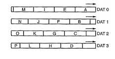
도 1을 참조하면, 상기 배경 기술 분에서 설명된 종류의 기존 MMC 카드(10)는 소켓(20)의 슬롯(19)에 삽입될 수 있다. 카드(10)는 카드의 표면에 한 단변을 따라 연장하는 7개의 전기 접촉부(11-17) 줄을 포함한다. 소켓(20)은 각 라인(21-27)에 연결된 7개의 대응 접촉핀(1-7)을 포함한다. 카드 접촉부(12)는 호스트로부터 명령 신호를 직렬로 수신하고 응답(상태신호)을 호스트에 직렬로 송신한다. 따라서 대응 소켓핀(2)은 명령/응답("CMD") 라인(22)에 연결된다. 직렬 데이터는 카드 접촉부(17)를 통해 수신되어 그 비휘발성 메모리에 저장되며, 이 메모리로부터 판독 시에 접촉부(17)를 통해 전송된다. 카드 접촉부(17)와 대응하는 소켓핀(7)에 연결된 라인(27)은 소켓 직렬 데이터("DAT") 라인이다. 이들 두 개의 라인(22, 27)은, 소켓핀(5)을 통해 전자 접촉부(15)와 연결된 클록 신호 입력라인(25)과 함께, 호스트 컴퓨터 기타 다른 장치와의 인터페이스를 제공하여 카드(10) 내의 메모리 시스템을 동작시킨다. 3개의 카드 접촉부(13, 14, 16)는 호스트 컴퓨터나 장치로부터 동작 전압을 수신하며, 각자의 소켓핀(3,4, 6)을 통해 외부 라인(23("Vss"), 24("Vdd"), 26("Vss2"))에 연결된다. 카드 접촉부(11), 따라서 소켓핀(1)과 라인(21)은 사용되지 않으며 다만 장래 이용을 위해 포함되어 있다.Referring to FIG. 1, an existing
각 MMC 카드(10) 내의 메모리 및 제어기 시스템의 관련 부분들은 도 2에 도시되어 있다. 플래시 EEPROM 셀의 어레이(31)는 디지털 데이터의 비휘발성 저장을 제공한다. 제어기(33)는 어레이(31) 동작을 관리하며 카드 접촉부(12-17)를 통해 호스트 시스템과 인터페이스한다. 접촉부(17)를 통해 직렬로 수신된 데이터는 레지스터(35)에 기록되고, 데이터 저장 버퍼 메모리(36) 내로 병렬로 전송되고, 다시 이 버퍼 메모리(36)로부터 제어기(33)로 전송된 다음에 메모리 셀 어레이(31)로 전송되어 여기에 저장된다. 반대로, 메모리 셀 어레이(31)로부터 판독된 데이터는 제어기(33)에 의해 버퍼 메모리(36)에 병렬로 전송되고, 다시 이 버퍼 메모리(36)로부터 레지스터(35)에 병렬로 전송된다. 그 다음, 이 판독된 데이터는 카드 접촉부(17)를 통해 레지스터(35) 밖으로 직렬 전송된다.The relevant parts of the memory and controller system in each
마찬가지로, 호스트로부터의 명령은 접촉부(12)를 통해 직렬 전송되어 레지스터(37)에 저장된 다음에, 제어기(33)에 의해 병렬로 판독된다. 상태 정보는 제어기(33)에 의해 레지스터(39)내로 병렬로 로드되고, 그 후 카드 접촉부(12)를 통해 직렬로 판독된다. 이런 식으로 전송되는 명령과 응답의 종류는 많이 있다. 예컨대, 호스트가 어레이(31) 내에 데이터를 기록해 넣고자 한다면, 기록 명령을 CMD 라인(22)을 통해 전송하고 이어서 기록될 데이터를 DAT 라인(27)을 통해 전송한다. 명령을 받은 기록 동작이 완료된 후에는 제어기(33)는 그 상태 표시를 레지스터(39)에 기록해 넣고, 그러면 호스트는 그 상태를 판독하여 그 명령을 받은 동작이 완료되었는지를 확인할 수 있다.Similarly, commands from the host are serially transmitted through
MMC 카드(10)에는 몇 가지 다른 레지스터들이 구비되어 있는데, 그 중 3개가 도 2에 도시되어 있다. 메모리 카드 식별 CID 레지스터(41)는 사용자에 의해 기록될 수 없고, 다만 각 카드에 고유한 식별을 호스트에 제공하도록 판독만이 될 수 있다. 상대 카드 주소 레지스터(RCA, 42)는 초기화 중에 그리고 카드가 시스템 내에 추가되거나 교체되는 경우에 호스트에 의해서 멀티카드 시스템 내에 어떤 주소가 기록되고, 후에 각 카드는 이 주소를 이용하여 공통 CMD 라인(22) 상의 명령이 그 카드를 위한 것인지 여부를 판단하게 된다. 상대 주소의 길이는 고유 주소를 가질 필요가 있는 시스템 내의 카드 수에 따라서 몇 비트만 되어도 된다. 이것은 CID 레지스터(41)에 저장된 제조자의 교유 식별보다 훨씬 짧으며, 따라서 이 상대 주소를 이용하게 되면 카드에 주소를 빨리 할당할 수 있게 된다. 호스트로부터의 각 명령은 시스템 내의 한 카드의 RCA 레지스터(42) 내에 이미 기록된 상대 주소를 수반하거나 포함하며, 따라서 그 카드는 응답하여 그 명령을 실행하는 반면에 RCA 레지스터(42) 내에 다른 상대 주소가 기록되어 있는 시스템의 다른 카드들은 응답하지 않는다.The
카드 특정 데이터 레지스터(43)("CSD")는 특정 메모리 어레이(31)와 제어기(33)의 데이터 포맷 정보, 데이터 액세스 특성 및 그와 유사한 정보를 포함한다. 이 데이터의 대부분은 제조자에 의해 기록되므로 사용자가 재기록할 수 없다. CSD 레지스터 데이터는 호스트에 의해 사용되어 시스템의 카드들과 통신 시에, 전송되는 데이터의 포맷, 데이터 액세스 방법 및 그와 유사한 것들을 포함하는 그 파라미터를 설정한다.The card specific data register 43 (" CSD ") contains data format information, data access characteristics, and the like of the
그와 같은 메모리 시스템은 도 3에 도시되어 있는데, 여기서는 개인용 컴퓨터, 휴대형 장치, 디지털 카메라, 오디오 재생 시스템 기타 그와 유사한 종류의 장치일 수 있는 호스트 장치(51)가 라인(22-27)을 통해 각자의 MMC 카드(59, 61, 63)를 수용하는 복수의 카드 소켓(53, 55, 57)와 연결된다. 그와 같은 멀티카드 시스템은 적어도 두 개의 그와 같은 소켓을 포함하며, 종종 더 많이 포함한다. 전술한 바와 같이, 명령과 응답은 시스템에서 각 소켓의 핀(2)과 연결된 단일 CMD 라인(22)을 통해 통신된다. 소켓에 삽입된 카드들(59, 61, 63) 중 한 카드의 RCA 레지스터(42)(도 2)에 저장된 고유 상대 주소는 명령과 함께 또는 명령의 일부로서 호스트(51)에 의해 전송되어 수용할 이들 카드들 중 한 카드만의 주소를 할당하고 그 명령에 따라 작동한다. 마찬가지로 각 소켓의 핀(7)과 연결된 단일 DAT 라인(21)을 통해 호스트와 카드 간에 데이터가 전송된다. 일정 주파수 클록 신호도 단일 라인(25)을 통해 호스트로부터 각 소켓의 핀(5)으로 전송된다(도 3에는 미도시). MMC 사양에서는 클록 주파수로서 20 메가헤르츠까지 요구한다.Such a memory system is shown in FIG. 3, where a
각 카드의 RCA 레지스터(42) 내에 고유 상대 주소를 기록해 넣기 위해 호스트에 의해 현재 이용되는 기술은 상대 주소가 존재하기 전에 호스트가 한번에 하나씩 각 카드에 주소를 할당할 수 있도록 해주는 각 카드 내의 회로를 이용한다. 호스트는 각 카드에게 각 카드의 CID 레지스터(41) 내에 영구적으로 기록된 제조자 식별 번호에 대해서 한 번에 한 비트씩 판독하라고 명령한다. 각 카드는 그 식별 코드의 비트에 따라서 개방 드레인 회로를 통해 공통 명령 및 응답 라인(22) 상의 전압에 영향을 미치기 쉽다. 그 라인 전압이 판독된 비트값에 의해 발생될 수 있는 것과 다르다면, 카드는 그 자신을 무동작 상태로 전환시킨다. 호스트가 카드들 중 한 카드만이 연결 상태를 유지하고 있다고 판단하면, 명령 및 응답 라인(22)을 통해 그 카드의 RCA 레지스터(42)에 고유 상대 주소를 기록한다. 그 다음, 이 카드는 그 자신을 명령 및 응답 라인(22)으로부터 단절시키고, 고유 상대 주소가 시스템 내의 각 카드의 CID 레지스터 내에 기록될 때까지 나머지 카드에 대해 처리를 계속한다.The technique currently used by the host to write a unique relative address in the RCA register 42 of each card utilizes circuitry within each card that allows the host to assign addresses to each card one at a time before the relative address exists. . The host instructs each card to read one bit at a time for the manufacturer identification number permanently recorded in the CID register 41 of each card. Each card is likely to affect the voltage on the common command and
SD 카드 및 시스템에 대한 설명Description of SD Cards and Systems
다중 명령/응답 라인의 이용Use of multiple command / response lines
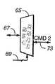
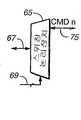
도 4에는 임의의 의미있는 방식으로 카드의 내부회로를 변경하지 않고서 다중 카드에 개별 주소를 보다 쉽게 할당할 수 있게 하는 변형된 시스템이 도시되어 있는데, 이 도면에서 도 1-3의 요소들과 공통되는 요소들에 대해서는 도일한 도면부호가 병기되어 있다. 호스트(51')는 호스트(51)(도 3)와 유사하나 메모리 카드의 명령/응답 라인과는 다르게 인터페이스하는 제어기(52)를 포함한다. 각 소켓의 핀(2)에 연결되어 있는 공통 명령 및 응답 라인 대신에, 별도의 라인(71, 73, 75)이 각 소켓(53, 55, 57)의 핀(2)에 연결된다. 이 별도의 명령/응답 라인들(71, 73, 75) 각각은 회로(69) 내의 호스트로부터의 제어신호에 응답하여 개별 라인들(71, 73, 75) 중에서 제어기(52)의 단일 명령/응답 라인(67)을 스위칭시키는 동작을 하는 스위칭 논리장치(65)의 일 출력이다. 스위칭 논리장치(65)의 가능한 연결은 도 5A-D에 도시되어 있다. 스위칭 논리장치(65)는 도 5A-C 각각에 도시된 바와 같이 개별 소켓 명령/응답 라인(71, 73, 75) 중에서 임의의 것을 선택하여 라인(67)에 연결시킬 수 있다. 이들 경우 중에서 어떤 경우에서도 라인(69)과 라인들(71, 73, 75 등) 중 선택된 것과의 사이에서 논리장치(65)를 통한 모든 방향에서 신호가 통과한다. 도 5D에 도시된 다른 연결에서는, 라인들(71, 73, 75 등) 모두가 라인(67)에 함께 연결되어 있어 호스트는 모든 카드 소켓에 명령을 동시에 송출할 수 있게 된다. 그러나 논리장치(65)는 호스트가 카드로부터 응답을 수신하고 있는 시각에 단 하나의 카드 소켓 명령/응답 라인 만이 라인(67)에 연결될 수 있게 하는 것이 바람직하다. 물론, 3개의 개별 소켓 명령/응답 라인이 도시되어 있지만, 시스템이 단 두 개의 카드 소켓을 포함하고 있다면 두 개의 라인 만이 사용될 것이다. 시스템이 3개 이상의 카드 소켓을 포함하고 있다면, 3개 이상의 명령/응답 라인이 각 소켓마다 하나씩 사용될 것이다.FIG. 4 shows a modified system that makes it easier to assign individual addresses to multiple cards without changing the internal circuitry of the card in any meaningful manner, which is common to the elements of FIGS. 1-3 in this figure. The same reference numerals are given to the elements to be described. Host 51 'includes a
도 6에는 고유 상대 주소가 도 4의 시스템의 소켓 내에 삽입된 각 카드의 RC내 레지스터에 기록되도록 시스템에 의해 실행되는 단계들이 나타나 있다. 이 루틴은 시스템이 기동하거나 초기화되고 있는 동안에 수행된다. 이 루틴은 또한 새로운 카드가 소켓에 삽입되는 초기화 후에 수행되나, 이 때는 그 카드에 대해서만 수행된다. 호스트(51')와 각 카드 소켓(53, 55, 57)(도 4) 사이에는, 카드 삽입 또는 제거 시에 이를 호스트에 알리는 별도의 카드 검출회로가 연결된다.6 shows the steps performed by the system such that the unique relative address is written to a register in the RC of each card inserted into the socket of the system of FIG. This routine is executed while the system is starting up or initializing. This routine is also performed after initialization where a new card is inserted into the socket, but only for that card. Between the host 51 'and each
초기화 처리에서 제1 단계(77)는 스위칭 논리장치(65)가 명령/응답 라인(71, 73, 75) 중 어느 하나를 라인(67)에 연결시키게 하는 것이다. 다음 단계(79)에서, 호스트(51')는 선택된 명령/응답 라인이 연결되어 있는 소켓 내에 삽입된 카드의 CID 레지스터(41)를 판독한다. 이 처리의 목적은 단계(81)에서 행해지는 그 소켓 내에 카드가 존재하는지 여부를 판단하는 것이지만, CID는 통상적으로 호스트가 카드와 통신하는데 이용할 수 있는 카드 정보를 포함하고 있기 때문에 호스트에 의해 판독되고 저장된다. 그 소켓에서 카드가 검출되지 않으면, 단계(83)에 나타난 바와 같이 논리장치(65)는 명령/응답 라인들(71, 73, 75) 중 다른 라인을 선택하도록 스위칭되고, 단계(79, 81)를 반복 수행하여 새로이 선택된 명령/응답 라인이 연결된 소켓에 카드가 존재하는지 여부를 판단한다.The
주소 할당된 소켓에서 카드가 검출되면, 호스트는 단계(84)에 나타난 바와 같이 카드로부터 상대 주소를 요구한다. 이에 앞서, 특정 구현에 있어서는 주소 할당된 카드는 그 자신의 주소를 생성하여 이것을 그 자신의 RCA 레지스터에 기록해 넣는다. 그 다음, 단계(85)에 나타나 있는 바와 같이, 호스트는 주소 할당된 소켓 내의 카드로부터 그 주소를 판독하고, 그 판독된 주소가 카드 주소들에 대해 유지하고 있는 테이블을 검사하여 제시된 주소가 이미 다른 카드에 할당되었는지를 판단한다. 제시된 주소가 고유한 것으로 판단되면, 이 주소는 그 카드의 RCA 레지스터에 머무르고, 호스트는 단계(86)에 나타난 바와 같이 제시된 주소를 그 제시된 주소가 소켓 번호로서 유지하고 있는 카드 주소 테이블에 추가한다. 특정 예에서, 카드는 카드에 포함되어 있는 난수 생성기로부터 32비트 주소를 생성한다. 이러한 많은 비트를 가지고서는, 특히 단 몇 장의 카드 만을 갖고 있는 통상의 시스템에서는 한 카드가 다른 카드와 동일한 주소를 제시할 가능성은 거의 없다. 그러나 만 일 단계(85)에서 이전 주소와의 충돌이 존재하는 것으로 판단되면, 호스트는 카드에게 그 RCA 레지스터 내의 다른 주소를 생성하여 저장하게 하고 호스트 자신은 그 새로운 주소에 대해서 단계(84, 85)를 반복한다.If a card is detected in the addressed socket, the host requests a relative address from the card as shown in
바람직하지는 않지만 자신을 주소를 생성하는 각 카드에 대한 대안으로서, 호스트는 한번에 하나의 카드에 주소를 할당하고 많은 가능한 주소 중에서 고유 주소를 주소할당된 카드의 RCA 레지스터에 기록해 넣음으로써 각 카드에 고유 상대 주소를 할당할 수 있다.As an alternative to each card that generates an address, although not desirable, the host assigns an address to one card at a time and writes a unique address among the many possible addresses into the RCA registers of the addressed card, thereby uniquely matching each card. You can assign addresses.
하나의 카드에 대해 주소 할당 처리가 완료되면, 단계(87)로 표시된 다음 단계에서 논리장치(65)는 다음 개별 소켓과 연결되도록 증분되거나(단계83), 만일 모든 소켓에 대해 처리가 완료되면, 단계(89)에 나타난 바와 같이 논리장치(65)는 도 5D에 나타난 상태로 전환된다. 소켓(53, 55, 57) 내의 각 카드가 그 RCA 레지스터 내에 기록된 고유 상대 주소를 갖고 있는 것으로 확인된 후, 시스템은 모든 명령/응답 라인(71, 73, 75)을 함께 연결함으로써 도 3에 나타낸 상태로 다시 재구성된다. 그 다음, 호스트는 MMC 시스템의 경우에서처럼 모든 CMD1, CMD2, 및 CMDn 라인을 통해 동시에 시스템 내의 모든 카드에게 명령을 전송하나, 호스트는 논리장치(65)의 특성 때문에 한 번에 하나의 카드만으로부터 응답 신호를 수신하도록 연결된다.When address assignment processing is completed for one card, in the next step indicated by
이 시스템의 이점은 초기화 중에 각 카드에게 차례로 주소 할당되도록 해주는 MMC 내에 사용된 회로를 제거함으로써 SD 카드가 간단화될 수 있다는 것이다. 동시에, 기존의 MMC 카드도 도 4 및 5의 시스템에 사용될 수 있다. 이것을 원하는 경우, 호스트는 각 카드로부터 판독된 CID와 같은 것으로부터 SD 카드나 MMC 카드가 시스템의 각 소켓 내에 있는지를 인식한다. 그 다음, 호스트는 각 소켓에 그 소켓 내의 카드에 적합한 통신 프로토콜과 루틴을 적용한다. 예컨대 주소 할당 루틴과 카드 리셋 동작은 다른 절차로서 서로 다르다. SD 카드의 클록 속도는 25 메가헤르츠까지 높게 될 수 있으므로, 호스트는 시스템 내에 카드가 한 개만 사용되는 경우에 MMC 카드의 낮은 클록 속도를 선택할 것이다. 호스트에 양종류의 카드로 동작하는 능력이 갖추어지면, 사용자는 시스템 소켓들 중 어느 한 소켓에 삽입되는 메모리 카드가 새로운 SD 카드인지 아니면 기존의 MMC 카드인지를 구별할 필요가 없다.The advantage of this system is that the SD card can be simplified by eliminating the circuitry used in the MMC that allows each card to be addressed in turn during initialization. At the same time, existing MMC cards can also be used in the systems of FIGS. 4 and 5. If desired, the host knows whether the SD card or MMC card is in each socket of the system, such as from the CID read from each card. The host then applies the appropriate communication protocol and routine to each socket for the card in that socket. For example, address assignment routines and card reset operations are different as different procedures. The clock speed of the SD card can be as high as 25 MHz, so the host will choose the lower clock speed of the MMC card if only one card is used in the system. If the host is capable of operating as both types of cards, the user does not have to distinguish between whether the memory card inserted into one of the system sockets is a new SD card or an existing MMC card.
대안으로서, 도 4 및 5의 시스템의 개별 소켓 명령/응답 라인은 MMC 시스템에서 현재 행해진 명령을 가진 또는 그 명령의 일부로서 상대 주소를 포함하지 않고서, 개별 소켓에 모든 명령을 전송하는데 사용될 수 있지만, 그렇게 되면 새로운 시스템은 MMC 카드와 호환될 수 없고 또 이 새로운 시스템에서는 호스트는 카드 종류마다 다르게 통신하여야 한다.Alternatively, the individual socket command / response lines of the systems of FIGS. 4 and 5 can be used to send all commands to individual sockets without including the relative address with or as part of the command currently made in the MMC system, The new system is then incompatible with the MMC card, and in this new system the host must communicate differently from card to card.
새로운 SD 카드 시스템의 다른 이점은 호스트가 주어진 주소의 카드가 삽입되는 소켓을 안다는 것이다. 이것은 그 소켓에 대한 CMD 라인이 동작하고 있지 않는 동안에 그 주소가 카드의 RCA 레지스터 내로 로드되기 때문이다. 이것은 카드가 대체되거나 새로운 카드가 추가되는 상황을 조정하는 것을 더욱 쉽게 해준다. SD 카드의 경우에는 새로운 카드만이 초기화의 일부로서 주소를 할당할 필요가 있다. MMC 시스템에서는 단 하나의 CMD 라인만이 존재하므로, 호스트는 특정 카드가 삽입되는 소켓을 알 수 없다. MMC 시스템에의 카드의 대체 또는 추가를 위해서는 시스템 내의 모든 카드를 초기화시킬 필요가 있으므로 시스템이 계속 동작하기 전에 지연이 생긴다.Another advantage of the new SD card system is that the host knows the socket into which the card at the given address is inserted. This is because the address is loaded into the card's RCA register while the CMD line for that socket is not running. This makes it easier to adjust the situation in which cards are replaced or new cards are added. In the case of an SD card, only the new card needs to be assigned an address as part of the initialization. Since there is only one CMD line in the MMC system, the host does not know the socket into which a particular card is inserted. Replacement or addition of cards to the MMC system requires the initialization of all cards in the system, resulting in a delay before the system continues to operate.
선택가능한 데이터 버스폭Selectable Data Bus Width
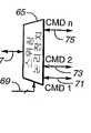
본 발명의 제2 양상은 도 7-12에 도시되어 있는데, 여기서는 새로운 SD 카드의 데이터 전송 특성이 기술된다. 호스트와 개별 카드 사이에 데이터가 전송되는 속도는 데이터가 동시에 전송되는 각 카드 소켓에 연결된 데이터 라인의 수를 증가시킴으로써 증가된다. 이 예에서는 4개의 데이터 라인이 도시되어 있는데, 이것은 데이터 전송 속도를 4배까지 증가시킬 수 있다. 데이터는 호스트와 MMC 카드 사이의 다중 데이터 라인 중 어느 하나의 데이터 라인만을 통해 전송된다. SD 카드의 특정 구현에서 한번에 사용되는 데이터 라인의 수는 하나 또는 4개이다.A second aspect of the invention is shown in Figures 7-12, where the data transfer characteristics of the new SD card are described. The rate at which data is transferred between the host and individual cards is increased by increasing the number of data lines connected to each card socket where data is simultaneously transmitted. In this example, four data lines are shown, which can increase the data transfer rate by four times. Data is transmitted over only one data line of the multiple data lines between the host and the MMC card. In a particular implementation of an SD card, the number of data lines used at one time is one or four.
SD 카드(90)와 이에 대응하는 소켓(100)은 도 7에 도시되어 있다. 도 4-6과 관련하여 전술한 본 발명의 제1 양상은 도 1의 MMC 카드(10)와 동일한 수의 접촉부를 가진 카드로 구현될 수 있지만, 본 발명의 제2 양상에서는 SD 카드는 더 많은 전기 접촉자 수를 가질 수 있다. SD 카드(90)는 도 1의 MMC 카드(10)와 동일한 접촉부(11-17)를 가지나, 동일한 상대 위치에서 데이터 전송을 위해 2개의 새로운 접촉부(91, 92)가 추가된다. 이제는 MMC 카드의 여분의 접촉부(11)도 데이터 전송을 위해 SD 카드에 의해 사용된다. 따라서, 카드(90) 내의 메모리 안팎으로 데이터를 전송하는데 4개의 접촉부(11, 17, 91, 92)가 SD 카드에 의해 사용된다. 마찬가지로 대응 소켓(100)(도 7)도 도 1의 소켓(20)과 동일한 핀(1-7)을 가지면서 2개의 핀(8, 9)이 추가된다. 그 결과는 각 카드 소켓에 연결된 4개의 데이터 라인(27(핀(7)), 101(핀(8)), 102(핀(9)), 및 21(핀(1)))이다.The
도 8에는 변형 시스템이 도시되어 있는데, 여기서는 호스트(51')가 각각 소켓(100)(도 7)를 가진 다중 소켓(104, 106, 108) 각각으로의 하나 이상의 데이터 라인을 통한 데이터의 동시 전송이 가능하도록 변형되어 있다. 4개의 데이터 라인(21, 27, 101, 102)은 스위칭 논리회로(110, 111, 112, 113)를 통해 멀티플렉서(105)와 각 소켓에 공통으로 연결된다. 각 소켓(106-108)에 삽입된 카드에 저장될 라인(107)에서의 단일 데이터열은, 라인(109)에서의 호스트 제어기(52')로부터의 제어 신호에 응답하여, 멀티플렉서에 의해서 4개의 스위칭 논리회로(110-113) 중에서 시계열적으로 교대로 스위칭된다. 마찬가지로, 데이터가 카드로부터 판독되고 있으면, 그와 같은 데이터열은 회로들(110-113) 간을 스위칭하는 멀티플렉서(105)에 의해서 라인(107)에서 조립된다.8 shows a variant system, where the host 51'concurrent transmission of data over one or more data lines to each of the
카드 소켓들에 연결된 다중 데이터 라인 각각에는 스위칭 논리회로(110-113) 중 하나가 구비되는데, 데이터 라인(DAT0)에는 회로(110)가, 데이터 라인(DAT1)에는 회로(111)가, 데이터 라인(DAT2)에는 회로(112)가, 그리고 데이터 라인(DAT3)에는 회로(113)가 구비된다. 이들은 호스트 제어기(52')에 연결된 라인들(114) 상의 신호에 의해 제어된다. 다중 소켓(104, 106, 108) 중 임의의 소켓 내의 카드에의 기록 동작 중에는 각 스위칭 논리회로(110-113)는 4개의 그 출력 전부가 입력에 연결된다. 따라서 기록될 데이터는 모든 소켓으로 송출된다. 그러나, 카드들 중 한 카드로부터 데이터가 판독되고 있으면, 각 회로(110-113)는 판독되고 있는 메모리 카드가 삽입된 소켓에 연결된 출력 라인만을 입력 라인에 연결하도록 스위칭된다.Each of the multiple data lines connected to the card sockets is provided with one of the switching logic circuits 110-113, a
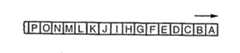
다중 데이터 라인을 수용하기 위해서, 도 2의 데이터 레지스터(35)와 그 동작은 SD 카드에서 특정 예로서 도 9 및 10A-E에 도시된 방식으로 변형된다. 기록 중에는 호스트 제어기(52')(도 8)는 라인(107)에 단일 데이터 열을 생성한다. 이 데이터 열은 도 10A에 도시되어 있으며, 여기서 문자 A, B, C 등은 각각 1 데이터 비트를 나타낸다. 멀티플렉서(105)는 1비트만의 전송을 위해 논리회로(110-113)를 한번에 하나씩 순차적으로 라인(107)에 연결한다. 이것은 4개의 데이터 접촉부를 가진 메모리 카드의 경우에 대해서 도 10B에 도시되어 있으며, 따라서 4개의 데이터 라인(DAT0, DAT1, DAT2, DAT3)이 모두 사용되고 있는 경우이다. 멀티플렉서(105)는 데이터 라인(DAT0)을 통해 제1 비트(A)를, 데이터 라인(DAT1)을 통해 제2 비트(B)를, 데이터 라인(DAT2)을 통해 제3 비트(C)를, 데이터 라인(DAT3)을 통해 제4 비트(D)를 전송하고, 그런 다음에 비트(E)를 데이터 라인(DAT0)에 전송하는 등과 같이 하여 처음부터 다시 시작한다. 이들 4개의 데이터 열은 데이터 레지스터(35')에 의해 수신되어 도 10A의 데이터 계열로 재조립된 다음에, 회로(38')를 통해서 도 2의 버퍼(36)와 같은 데이터 버퍼에 병렬로 전송된다. 각 개별적인 직렬 데이터 열은 그 비트를 블록의 데이터로부터 계산된 주기적 중복성 검사("CRC") 비트를 포함하는 블록 내로 축적함으로써 각자의 데이터 라인을 통해 전송되는 것이 바람직하다. 특정 예로서 각 블록은 개시 비트, 그 다음에는 데이터, 그 다음에는 CRC, 그 다음에는 중지 비트를 포함한다.In order to accommodate multiple data lines, the data register 35 and its operation in FIG. 2 are modified in the manner shown in FIGS. 9 and 10A-E as a specific example in the SD card. During writing, host controller 52 '(FIG. 8) creates a single data string on
데이터 라인들의 어느 것도 그 데이터 전송 속도가 제한되어 있지만, 다중 데이터 라인을 통한 동시 데이터 전송은 대략 데이터 라인 수와 같은 배수 만큼 그 속도를 증가시킨다. 만일 예컨대 두 개의 데이터 라인이 사용되고 있다면, 도 10A의 데이터 전송 속도의 절반의 전송 속도를 가진 도 10C에 도시된 데이터열이 라인(107)에서 공급된다. 그 다음, 멀티플렉서(105)는 데이터 라인(DAT0)과 데이터 라인(DAT1) 간에서 이 데이터열을 스위칭하여 도 10D에 도시된 바와 같은 데이터열이 되게 한다. 그 다음, 주소 할당된 카드에서의 데이터 레지스터(35')는 두 개의 데이터열(DAT0, DAT1)을 재조립하여 도 10C의 데이터열로 만들고, 이 데이터열을 라인(38')을 통해 병렬로 전송한다. 만일 단 한 개의 데이터 라인이 사용되고 있다면, 멀티플렉서(105)는 DAT0과 같은 하나의 데이터 라인과 연결을 유지하고, 이 데이터 라인을 통해서, 감소된 데이터 속도를 가진 라인(1070에서의 데이터열이 도 10E에 도시된 바와 같이 전송된다.While none of the data lines has a limited data transfer rate, simultaneous data transfers over multiple data lines increase their speed by approximately a multiple of the number of data lines. If, for example, two data lines are used, the data string shown in Fig. 10C with a transfer rate of half the data transfer rate of Fig. 10A is supplied at
반대로, 메모리로부터 데이터가 판독되고 있으면, 데이터는 레지스터(35') 내로 병렬로 로드되고, 사용되고 있는 데이터 라인의 수에 따라서 도 10B, 10D 또는 10E에 도시된 포맷들 중 어느 한 포맷을 가지고서 데이터 라인들을 통해 전송된다. 만일 데이터가 하나 이상의 데이터 라인을 통해 전송되고 있으면, 사용되고 있는 데이터 라인의 수에 따라서 도 10A, 10C 또는 10E 중 어느 하나의 데이터열에 해당하는 라인(107)에서의 데이터열이 되게하기 위하여 멀티플렉서(105)는 사용되고 있는 데이터 라인들 중에서 앞뒤로 스위칭한다.Conversely, if data is being read from the memory, the data is loaded in parallel into the register 35 'and the data line has either of the formats shown in Figures 10B, 10D or 10E depending on the number of data lines being used. Are sent through the network. If data is being transmitted over one or more data lines, the
도 8의 시스템에 있어서는 시스템 내에 구비된 데이터 라인의 수(이 예에서 는 4개의 라인)까지 하나, 둘 또는 기타의 수처럼 여러 가지 수의 데이터 라인 접촉부를 가진 카드를 수용할 수 있도록 하고, 이 시스템에서 그와 같은 카드들을 자유로이 혼합하고 교환할 수 있게 하는 것이 바람직하다. 일부 응용에 있어서는, 시스템의 데이터 라인 수(이 경우에는 4개)에 의해 제공되는 높은 데이터 전송 속도가 필요하지 않다. 이러한 응용에 있어서는 더 적은 수의 데이터 핀을 갖도록 SD 카드가 변형된다. 그에 따라서 카드 내의 인터페이스 회로의 수도 줄어들게 되며, 따라서 카드 가격이 감소된다. 단 하나의 동작 데이터 핀을 가진 카드와 마찬가지로 두 개의 동작 데이터 핀을 가진 카드도 유용하다.In the system of FIG. 8, it is possible to accommodate cards with various numbers of data line contacts, such as one, two, or the like, up to the number of data lines provided in the system (four lines in this example). It is desirable to allow such cards to be freely mixed and exchanged in the system. In some applications, the high data transfer rate provided by the number of data lines in the system (four in this case) is not necessary. In these applications, the SD card is modified to have fewer data pins. This reduces the number of interface circuits in the card, thus reducing the card price. Like cards with only one operational data pin, cards with two operational data pins are useful.
동일한 시스템에서 서로 다른 수의 데이터 라인을 가진 카드를 이용할 수 있기 위해서는, 호스트에 의해 판독되는 개별 카드에 호스트가 그 카드와 통신할 수 있는 데이터 라인의 수를 판단하기 위한 판독 전용 필드를 구비하는 것이 바람직하다. 특정 구현에서 이것은 MMC 카드에 대한 도 2에 도시된 레지스터에 추가된 SD 카드 구성 레지스터("SCR")에 포함된다. 호스트(51')는 이 필드를 기동 시에, 여러 가지 다른 시점에서 초기화 시에 즉 새로운 카드가 소켓에 삽입될 때마다 판독하고, 그 후에 각 카드에 주소 할당된 데이터를 카드가 수용할 수 있는 수의 데이터 라인을 통해 전송한다. 그러나, 추가된 각 데이터 라인에 필요한 추가 회로를 제공하는데 비용이 들기 때문에, 일부 카드들은 더 적은 수의 데이터 라인으로 동작하도록 설계된다. 반대로, 호스트는 가능한 것보다 더 적은 수의 데이터 라인으로 동작하도록 설계된다. 특정 응용에 있어서 데이터 전송 속도를 높일 필요가 없다면, 카드와 호스트 시스템 양쪽에서 높은 데이터 전송 속도를 제공하는데 추가되 는 복잡성과 비용을 피할 수 있다.In order to be able to use cards with different numbers of data lines in the same system, it is necessary to have a read-only field on each card read by the host to determine the number of data lines the host can communicate with the card. desirable. In a particular implementation this is included in the SD card configuration register (“SCR”) added to the register shown in FIG. 2 for the MMC card. The host 51 'reads this field at startup, at different points of time at initialization, each time a new card is inserted into the socket, and then the card can accept the data addressed to each card. Transmit over a number of data lines. However, because of the cost of providing the additional circuitry required for each additional data line, some cards are designed to operate with fewer data lines. In contrast, a host is designed to operate with fewer data lines than possible. If you do not need to increase the data rate for a particular application, you can avoid the added complexity and cost of providing high data rates on both the card and the host system.
호스트와 하나 또는 그 이상의 메모리 카드 간의 데이터 버스의 폭을 동적으로 선택할 수 있다면 호스트는 시스템에 어떤 메모리 카드가 삽입되더라도 그 카드와 호스트 간의 데이터 전송 속도를 극대화할 수 있다. 다중 데이터 라인들 간의 데이터열을 분해하는 다른 기술도 가능하지만, 도 10A-10E에 도시된 전술한 기술들은 호스트를 서로 다른 데이터 버스 폭을 가진 카드에 적응시키는데 바람직하며, 동적으로 그렇게 하기 위해서 카드는 대체 또는 추가되고, 개별 카드의 최대 데이터 라인 수를 이용함으로써 서로 다른 데이터 버스 폭을 가진 카드 혼합체의 각 카드와 통신한다. 다른 기술은 각 데이터 라인을 따라 다중 계열 데이터 비트의 전송 패킷을 교대시키는 것이다. 그러나 이를 위해서는 패킷 등의 진로를 추적하는데 오버헤드가 소요된다. 특히 시스템이 서로 다른 수의 데이터 라인을 가진 카드들에 적응할 필요가 있는 때에는 전술한 바와 같이 한번에 한 비트씩 다중 병렬 데이터 경로를 통해 데이터열의 연속 비트들을 교대하는 것이 더 간단하다, 실제로는 이 데이터 전송 기술은 여기에 설명되는 메모리 시스템이 아닌 다른 분야에 응용된다.If the width of the data bus between the host and one or more memory cards can be dynamically selected, the host can maximize the data transfer rate between the card and the host no matter what memory card is inserted into the system. Other techniques for decomposing data sequences between multiple data lines are possible, but the techniques described above in FIGS. 10A-10E are desirable for adapting the host to cards with different data bus widths, and in order to do so dynamically, It is replaced or added and communicates with each card of the card mix with different data bus widths by using the maximum number of data lines of the individual cards. Another technique is to alternate transmission packets of multiple series of data bits along each data line. However, this requires overhead to track the path of the packet. In particular, when the system needs to adapt to cards with different numbers of data lines, it is simpler to alternate successive bits of the data string through multiple parallel data paths, one bit at a time, as described above. The technology is applied to other fields than the memory system described herein.
도 11의 흐름도는 도 7-10E의 메모리 시스템을 동작시키는 방법의 일 양상을 도시한 것으로, 여기서 호스트(51'')는 두 개 또는 그 이상의 소켓(104, 106, 108)에 설치된 각 카드가 동작하도록 설계된 데이터 라인의 수를 확인한다. 제1 단계(121)에서, 호스트는 RCA 레지스터(42)(도 2)에 이미 기록되어 있는 카드의 상대 주소를 이용하여 명령/응답 라인(22)을 통해 카드들 중 어느 한 카드에 주소를 할당한다. 다음, 단계(125)에서, 호스트에 의해 그 카드에 대한 데이터 라인의 수가 SCR 레지스터로부터 판독된다. 그 다음, 단계(125)에 나타난 바와 같이 이 수는 호스트에 의해 바람직하게는 테이블 형태로 저장된다. 시스템의 소켓 내의 모든 카드가 판독되었다면, 처리는 종료되고, 만일 그렇지 않으면, 단계(129)에서 시스템의 다른 카드들에 주소가 할당되고, 이 다른 카드들에 대해서 단계(123, 125)가 반복된다.11 illustrates one aspect of a method of operating the memory system of FIGS. 7-10E wherein the
도 12는 시스템 내의 카드들에 대한 데이터 라인의 수에 대한 저장된 데이터를 호스트(51'')가 어떻게 이용하는 가를 보여주는 흐름도이다.12 is a flowchart showing how the
단계(131)에 나타난 바와 같이 호스트에 의해 특정 카드 소켓에 주소가 할당될 때마다 호스트는 도 11의 처리에 의해 구축된 내부 테이블로부터 그 카드에 대한 데이터 라인 수를 판독한다. 그 다음, 단계(135)에 나타난 바와 같이, 호스트는 멀티플렉서(105)를 동작시켜 그 테이블로부터 판독된 4개의 데이터 라인(DAT0, DAT1, DAT2, DAT3)을 통해 데이터를 전송한다. 다음 단계(137)에서, 그 수의 데이터 라인을 통해 데이터가 카드로부터 또는 카드 쪽으로 전송된다. 특정 예에서 하나의 데이터 라인만을 가진 카드의 경우에서는 호스트는 MMC 제품과 동일한 카드 접촉부(17)를 이용하기 때문에 따라서 시스템이 MMC 카드와 호환성을 가질 수 있기 때문에 라인(27)(DAT0)을 통해 카드에 데이터를 전송하는 것이 바람직하다. MMC 카드는 SD 카드는 물론 도 8-10E의 시스템에서도 사용될 수 있다. 호스트는 카드가 MMC 카드인지 SD 카드인지를 판단하기 위하여 초기화 중에 DAT0 라인만을 통해 각 카드와 통신하는 것이 바람직하며, 만일 SD 카드인 경우에는 이 카드가 사용하 는 데이터 라인의 수와 기타 그 기타에 대한 정보에 의해서 시스템은 효율적으로 동작할 수 있게 된다.Each time an address is assigned to a particular card socket by the host as shown in
도 8의 시스템은 MMC 설계에 따른 단일 명령/응답 라인(22)(미도시)이나 도 4-6과 관련하여 전술한 다중 명령/응답 라인 시스템을 사용할 수 있다. 이에 대한 선택은 카드의 구조나 회로에 영향을 미치지 않는다.The system of FIG. 8 may use a single command / response line 22 (not shown) according to the MMC design or the multiple command / response line system described above with respect to FIGS. 4-6. This choice does not affect the card's structure or circuitry.
지금까지 특정 실시예들을 통해서 본 발명의 여러 가지 양상을 설명하였지만, 본 발명은 첨부된 청구범위 내에서 보호되어야 함은 마땅할 것이다. 특히, 본 발명은 특정 수의 데이터 라인이나 메모리 카드를 가진 시스템에 한정되지 않으며, 이러한 특정 수는 본 발명의 설명에서는 예시 목적으로만 선택된 것일 뿐이다.While various aspects of the invention have been described with reference to specific embodiments so far, it will be appreciated that the invention is intended to be protected within the scope of the appended claims. In particular, the present invention is not limited to a system having a specific number of data lines or a memory card, and this specific number is only selected for illustrative purposes in the description of the present invention.
Claims (42)
Translated fromKoreanApplications Claiming Priority (3)
| Application Number | Priority Date | Filing Date | Title |
|---|---|---|---|
| US09/641,023US6820148B1 (en) | 2000-08-17 | 2000-08-17 | Multiple removable non-volatile memory cards serially communicating with a host |
| US09/641,023 | 2000-08-17 | ||
| PCT/US2001/025550WO2002015020A2 (en) | 2000-08-17 | 2001-08-14 | Multiple removable non-volatile memory cards serially communicating with a host |
Publications (2)
| Publication Number | Publication Date |
|---|---|
| KR20030033029A KR20030033029A (en) | 2003-04-26 |
| KR100932892B1true KR100932892B1 (en) | 2009-12-21 |
Family
ID=24570622
Family Applications (1)
| Application Number | Title | Priority Date | Filing Date |
|---|---|---|---|
| KR1020037002335AExpired - Fee RelatedKR100932892B1 (en) | 2000-08-17 | 2001-08-14 | Multiple removable nonvolatile memory cards in serial communication with the host |
Country Status (10)
| Country | Link |
|---|---|
| US (10) | US6820148B1 (en) |
| EP (13) | EP1903448B1 (en) |
| JP (3) | JP5048203B2 (en) |
| KR (1) | KR100932892B1 (en) |
| CN (1) | CN1208735C (en) |
| AT (1) | ATE386294T1 (en) |
| AU (1) | AU2001286495A1 (en) |
| DE (2) | DE60132780T2 (en) |
| TW (1) | TW561346B (en) |
| WO (1) | WO2002015020A2 (en) |
Families Citing this family (136)
| Publication number | Priority date | Publication date | Assignee | Title |
|---|---|---|---|---|
| KR100473308B1 (en)* | 1995-01-31 | 2005-03-14 | 가부시끼가이샤 히다치 세이사꾸쇼 | Nonvolatile memory device |
| US7295443B2 (en) | 2000-07-06 | 2007-11-13 | Onspec Electronic, Inc. | Smartconnect universal flash media card adapters |
| US6438638B1 (en)* | 2000-07-06 | 2002-08-20 | Onspec Electronic, Inc. | Flashtoaster for reading several types of flash-memory cards with or without a PC |
| US6820148B1 (en) | 2000-08-17 | 2004-11-16 | Sandisk Corporation | Multiple removable non-volatile memory cards serially communicating with a host |
| US7107378B1 (en) | 2000-09-01 | 2006-09-12 | Sandisk Corporation | Cooperative interconnection and operation of a non-volatile memory card and an input-output card |
| CN1720578A (en)* | 2000-12-07 | 2006-01-11 | 三因迪斯克公司 | System, method and apparatus for playback of recorded audio, video or other content from non-volatile memory card, compact disk or other media |
| US7275112B1 (en)* | 2001-08-08 | 2007-09-25 | Pasternak Solutions Llc | Efficient serialization of bursty out-of-order results |
| JP3552213B2 (en)* | 2001-08-31 | 2004-08-11 | 株式会社東芝 | SD memory card host controller and clock control method |
| JP4082913B2 (en)* | 2002-02-07 | 2008-04-30 | 株式会社ルネサステクノロジ | Memory system |
| US7092256B1 (en) | 2002-04-26 | 2006-08-15 | Sandisk Corporation | Retractable card adapter |
| US7367503B2 (en) | 2002-11-13 | 2008-05-06 | Sandisk Corporation | Universal non-volatile memory card used with various different standard cards containing a memory controller |
| US8037229B2 (en)* | 2002-11-21 | 2011-10-11 | Sandisk Technologies Inc. | Combination non-volatile memory and input-output card with direct memory access |
| US20050055479A1 (en)* | 2002-11-21 | 2005-03-10 | Aviad Zer | Multi-module circuit card with inter-module direct memory access |
| FI20022113L (en)* | 2002-11-29 | 2004-08-06 | Nokia Corp | Method and system for identifying bus width, electronic device and peripheral device |
| TW556910U (en)* | 2002-12-30 | 2003-10-01 | Carry Computer Eng Co Ltd | Reading device of card reader using SATA (Serial Advanced Technology Attachment) |
| GB2424105B (en) | 2003-01-13 | 2007-03-07 | Rambus Inc | Coded write masking |
| US7313639B2 (en) | 2003-01-13 | 2007-12-25 | Rambus Inc. | Memory system and device with serialized data transfer |
| US7305535B2 (en) | 2003-04-17 | 2007-12-04 | Sandisk Corporation | Memory cards including a standard security function |
| FI20035072A0 (en)* | 2003-05-22 | 2003-05-22 | Nokia Corp | Interface bus, electronic device and system |
| US6973519B1 (en)* | 2003-06-03 | 2005-12-06 | Lexar Media, Inc. | Card identification compatibility |
| KR100475125B1 (en)* | 2003-06-21 | 2005-03-14 | 삼성전자주식회사 | Movable storage apparatus capable of freely changing width of data bus and method for setting width of data bus of the same |
| US7036054B2 (en)* | 2003-07-02 | 2006-04-25 | Nokia Corporation | Memory bus checking procedure |
| KR100577392B1 (en) | 2003-08-29 | 2006-05-10 | 삼성전자주식회사 | Method and apparatus for improving transmission speed of multimedia card using difference signal |
| US7209995B2 (en) | 2003-12-09 | 2007-04-24 | Sandisk Corporation | Efficient connection between modules of removable electronic circuit cards |
| JP4515793B2 (en)* | 2004-03-11 | 2010-08-04 | 株式会社東芝 | Memory card device and memory card control method |
| TWI227500B (en)* | 2004-03-12 | 2005-02-01 | Winbond Electronics Corp | Operating method of read function of memory card having automatic adaptive function and card controller |
| US7152801B2 (en)* | 2004-04-16 | 2006-12-26 | Sandisk Corporation | Memory cards having two standard sets of contacts |
| US7487265B2 (en)* | 2004-04-16 | 2009-02-03 | Sandisk Corporation | Memory card with two standard sets of contacts and a hinged contact covering mechanism |
| US7269669B2 (en)* | 2004-07-07 | 2007-09-11 | Sychip Inc | Sharing single host controller with multiple functional devices |
| US7814377B2 (en)* | 2004-07-09 | 2010-10-12 | Sandisk Corporation | Non-volatile memory system with self test capability |
| US7427027B2 (en)* | 2004-07-28 | 2008-09-23 | Sandisk Corporation | Optimized non-volatile storage systems |
| KR100677127B1 (en)* | 2004-07-28 | 2007-02-02 | 삼성전자주식회사 | Method and device for automatic memory card switching in multifunction device |
| JP4799417B2 (en)* | 2004-09-28 | 2011-10-26 | dブロード株式会社 | Host controller |
| CN100524273C (en)* | 2004-10-01 | 2009-08-05 | 松下电器产业株式会社 | Memory card controller, memory card drive device, and computer program |
| WO2006057049A1 (en) | 2004-11-26 | 2006-06-01 | Kabushiki Kaisha Toshiba | Card and host device |
| JP4817836B2 (en) | 2004-12-27 | 2011-11-16 | 株式会社東芝 | Card and host equipment |
| JP4892852B2 (en)* | 2005-03-29 | 2012-03-07 | 富士通セミコンダクター株式会社 | Serial interface control method |
| JP2007011753A (en)* | 2005-06-30 | 2007-01-18 | Toshiba Corp | Information processing apparatus and control method thereof |
| JP4896450B2 (en)* | 2005-06-30 | 2012-03-14 | 株式会社東芝 | Storage device |
| US7710736B2 (en) | 2005-08-02 | 2010-05-04 | Sandisk Corporation | Memory card with latching mechanism for hinged cover |
| US7765350B2 (en)* | 2005-09-14 | 2010-07-27 | Koninklijke Philips Electronics N.V. | Method and system for bus arbitration |
| DE102005045149A1 (en)* | 2005-09-22 | 2007-04-05 | Giesecke & Devrient Gmbh | Method for initializing and / or personalizing a portable data carrier |
| US8661540B2 (en) | 2005-10-07 | 2014-02-25 | Imation Corp. | Method and apparatus for secure credential entry without physical entry |
| US7640424B2 (en)* | 2005-10-13 | 2009-12-29 | Sandisk Corporation | Initialization of flash storage via an embedded controller |
| US20070145135A1 (en)* | 2005-12-28 | 2007-06-28 | Fabrice Jogand-Coulomb | Methods used in a nested memory system with near field communications capability |
| US20070145152A1 (en)* | 2005-12-28 | 2007-06-28 | Fabrice Jogand-Coulomb | Nested memory system with near field communications capability |
| US7739487B2 (en)* | 2006-01-17 | 2010-06-15 | Nokia Corporation | Method for booting a host device from an MMC/SD device, a host device bootable from an MMC/SD device and an MMC/SD device method a host device may booted from |
| CN101166034B (en)* | 2006-06-13 | 2012-10-10 | 中宇科技有限公司 | Card-insertable audio playback device and method for identifying the card |
| US8661185B2 (en)* | 2006-07-12 | 2014-02-25 | Sandisk Technologies Inc. | Electronic library for managing data on removable storage devices |
| US20080016312A1 (en)* | 2006-07-12 | 2008-01-17 | Tyler Thorp | Method for Managing Data on Removable Storage Devices in an Electronic Library |
| US7696044B2 (en)* | 2006-09-19 | 2010-04-13 | Sandisk Corporation | Method of making an array of non-volatile memory cells with floating gates formed of spacers in substrate trenches |
| US7646054B2 (en)* | 2006-09-19 | 2010-01-12 | Sandisk Corporation | Array of non-volatile memory cells with floating gates formed of spacers in substrate trenches |
| US8327454B2 (en)* | 2006-11-14 | 2012-12-04 | Sandisk Technologies Inc. | Method for allowing multiple users to access preview content |
| US8079071B2 (en) | 2006-11-14 | 2011-12-13 | SanDisk Technologies, Inc. | Methods for accessing content based on a session ticket |
| US8763110B2 (en) | 2006-11-14 | 2014-06-24 | Sandisk Technologies Inc. | Apparatuses for binding content to a separate memory device |
| US7800161B2 (en)* | 2006-12-21 | 2010-09-21 | Sandisk Corporation | Flash NAND memory cell array with charge storage elements positioned in trenches |
| US7642160B2 (en)* | 2006-12-21 | 2010-01-05 | Sandisk Corporation | Method of forming a flash NAND memory cell array with charge storage elements positioned in trenches |
| KR100882207B1 (en)* | 2007-04-04 | 2009-02-06 | 삼성전자주식회사 | Memory device including a connector to interface other memory devices with the host independently |
| US8762640B2 (en)* | 2007-06-27 | 2014-06-24 | Sandisk Il Ltd. | Method for operating a memory interface with SIM functions |
| JP4473900B2 (en)* | 2007-08-22 | 2010-06-02 | 株式会社東芝 | Semiconductor memory device |
| WO2009027802A1 (en)* | 2007-08-28 | 2009-03-05 | Nokia Corporation | Method for bus testing and addressing in mass memory components |
| JP2009054103A (en)* | 2007-08-29 | 2009-03-12 | Panasonic Corp | Host device that controls multiple memory cards |
| US7774511B2 (en)* | 2007-10-11 | 2010-08-10 | Sandisk Il Ltd. | Addressing multiple devices on a shared bus |
| JP5124237B2 (en)* | 2007-11-02 | 2013-01-23 | 株式会社日立製作所 | Storage system and storage subsystem |
| USD588597S1 (en)* | 2007-12-17 | 2009-03-17 | Panasonic Corporation | IC memory card |
| USD588133S1 (en)* | 2007-12-17 | 2009-03-10 | Panasonic Corporation | IC memory card |
| USD588134S1 (en)* | 2008-01-11 | 2009-03-10 | Panasonic Corporation | IC memory card |
| KR101412524B1 (en) | 2008-01-31 | 2014-06-25 | 삼성전자주식회사 | Memory device, memory card system and method of recognizing the card |
| JP5166922B2 (en)* | 2008-03-10 | 2013-03-21 | キヤノン株式会社 | Shared bus control device and control method thereof |
| USD588599S1 (en)* | 2008-04-01 | 2009-03-17 | Panasonic Corporation | IC memory card |
| USD588135S1 (en)* | 2008-04-01 | 2009-03-10 | Panasonic Corporation | IC memory card |
| USD588598S1 (en)* | 2008-04-01 | 2009-03-17 | Panasonic Corporation | IC memory card |
| US20100017558A1 (en) | 2008-04-11 | 2010-01-21 | Richard Matthew Fruin | Memory device operable in read-only and re-writable modes of operation |
| US8862821B2 (en)* | 2008-07-08 | 2014-10-14 | Sandisk Il Ltd. | Portable device for managing memory cards |
| US8161219B2 (en)* | 2008-09-30 | 2012-04-17 | Qimonda Ag | Distributed command and address bus architecture for a memory module having portions of bus lines separately disposed |
| WO2010047059A1 (en)* | 2008-10-24 | 2010-04-29 | パナソニック株式会社 | Card host lsi, and set equipment possessing same |
| US8472199B2 (en) | 2008-11-13 | 2013-06-25 | Mosaid Technologies Incorporated | System including a plurality of encapsulated semiconductor chips |
| JP5269625B2 (en)* | 2009-01-14 | 2013-08-21 | 株式会社東芝 | Interface control device |
| WO2010083593A1 (en) | 2009-01-21 | 2010-07-29 | Memory Experts International Inc. | Removable memory storage device with multiple authentication processes |
| US20100205355A1 (en)* | 2009-02-11 | 2010-08-12 | Memory Experts International Inc. | Multiplexing secure digital memory |
| US8205037B2 (en)* | 2009-04-08 | 2012-06-19 | Google Inc. | Data storage device capable of recognizing and controlling multiple types of memory chips operating at different voltages |
| KR101606880B1 (en)* | 2009-06-22 | 2016-03-28 | 삼성전자주식회사 | Data storage system and channel driving method thereof |
| US8516232B2 (en)* | 2009-06-30 | 2013-08-20 | Sandisk Technologies Inc. | Method and memory device for performing an operation on data |
| US8312088B2 (en)* | 2009-07-27 | 2012-11-13 | Sandisk Il Ltd. | Device identifier selection |
| US8392614B2 (en)* | 2009-07-27 | 2013-03-05 | Sandisk Il Ltd. | Device identifier selection |
| US8291144B2 (en) | 2009-08-14 | 2012-10-16 | Sandisk Il Ltd. | Dual interface card with backward and forward compatibility |
| US8775825B2 (en) | 2009-08-17 | 2014-07-08 | Cram Worldwide Llc | Digital content management and delivery |
| JP5150591B2 (en) | 2009-09-24 | 2013-02-20 | 株式会社東芝 | Semiconductor device and host device |
| US8255655B2 (en)* | 2009-10-02 | 2012-08-28 | Sandisk Technologies Inc. | Authentication and securing of write-once, read-many (WORM) memory devices |
| US8690283B2 (en) | 2009-10-20 | 2014-04-08 | Sandisk Il Ltd. | Method and system for printing graphical content onto a plurality of memory devices and for providing a visually distinguishable memory device |
| USD638431S1 (en) | 2009-10-20 | 2011-05-24 | Sandisk Corporation | MicroSD memory card with a semi-transparent color surface |
| USD628202S1 (en) | 2009-10-20 | 2010-11-30 | Sandisk Corporation | MicroSD memory card with different color surfaces |
| EP2513743B1 (en) | 2009-12-17 | 2017-11-15 | Toshiba Memory Corporation | Semiconductor system, semiconductor device, and electronic device initializing method |
| JP2011159267A (en)* | 2010-02-03 | 2011-08-18 | Agile Patch Solutions Inc | Memory system with a plurality of replaceable nonvolatile memories |
| US7888966B1 (en) | 2010-03-25 | 2011-02-15 | Sandisk Corporation | Enhancement of input/output for non source-synchronous interfaces |
| US8085099B2 (en) | 2010-04-06 | 2011-12-27 | Sandisk Technologies Inc. | Self-calibrating relaxation oscillator based clock source |
| KR20110116710A (en)* | 2010-04-20 | 2011-10-26 | 삼성전자주식회사 | Apparatus and method for supporting a plurality of external memories in a portable terminal |
| US20120066453A1 (en)* | 2010-09-10 | 2012-03-15 | Action Star Enterprise Co., Ltd. | Card-reading device for multi cards |
| JP5728292B2 (en) | 2011-02-04 | 2015-06-03 | 株式会社東芝 | Memory device and host system |
| US9633391B2 (en) | 2011-03-30 | 2017-04-25 | Cram Worldwide, Llc | Secure pre-loaded drive management at kiosk |
| CN102736859A (en)* | 2011-04-08 | 2012-10-17 | 深圳富泰宏精密工业有限公司 | Double storage card control system and method |
| US8819484B2 (en) | 2011-10-07 | 2014-08-26 | International Business Machines Corporation | Dynamically reconfiguring a primary processor identity within a multi-processor socket server |
| USD667830S1 (en)* | 2011-11-29 | 2012-09-25 | Samsung Electronics Co., Ltd. | SD memory card |
| US20130151755A1 (en) | 2011-12-12 | 2013-06-13 | Reuven Elhamias | Non-Volatile Storage Systems with Go To Sleep Adaption |
| JP5790532B2 (en)* | 2012-02-13 | 2015-10-07 | セイコーエプソン株式会社 | Electronic device and memory control method |
| WO2013134366A1 (en)* | 2012-03-06 | 2013-09-12 | Burns Christopher J | Smartcard and computer quick connect and release system |
| KR20140027859A (en) | 2012-08-27 | 2014-03-07 | 삼성전자주식회사 | Host device and system including the same |
| US8904078B2 (en) | 2012-10-22 | 2014-12-02 | Lenovo Enterprise Solutions (Singapore) Pte. Ltd. | High speed serial peripheral interface system |
| USD729808S1 (en) | 2013-03-13 | 2015-05-19 | Nagrastar Llc | Smart card interface |
| USD758372S1 (en) | 2013-03-13 | 2016-06-07 | Nagrastar Llc | Smart card interface |
| US9888283B2 (en) | 2013-03-13 | 2018-02-06 | Nagrastar Llc | Systems and methods for performing transport I/O |
| USD759022S1 (en) | 2013-03-13 | 2016-06-14 | Nagrastar Llc | Smart card interface |
| US9647997B2 (en) | 2013-03-13 | 2017-05-09 | Nagrastar, Llc | USB interface for performing transport I/O |
| US9411721B2 (en) | 2013-11-15 | 2016-08-09 | Sandisk Technologies Llc | Detecting access sequences for data compression on non-volatile memory devices |
| US10114787B2 (en)* | 2014-02-03 | 2018-10-30 | Qualcomm Incorporated | Device identification generation in electronic devices to allow external control of device identification for bus communications identification, and related systems and methods |
| US9177654B2 (en) | 2014-03-26 | 2015-11-03 | Burst Corporation | Solid-state memory device with plurality of memory cards |
| USD736213S1 (en)* | 2014-07-01 | 2015-08-11 | Samsung Electronics Co., Ltd. | Memory card |
| USD736212S1 (en)* | 2014-07-01 | 2015-08-11 | Samsung Electronics Co., Ltd. | Memory card |
| KR102285789B1 (en) | 2014-07-01 | 2021-08-04 | 삼성전자 주식회사 | An external storage device, and a method of setting up a reference frequency of the same |
| USD739856S1 (en)* | 2014-07-30 | 2015-09-29 | Samsung Electronics Co., Ltd. | Memory card |
| USD736216S1 (en)* | 2014-07-30 | 2015-08-11 | Samsung Electronics Co., Ltd. | Memory card |
| USD780763S1 (en) | 2015-03-20 | 2017-03-07 | Nagrastar Llc | Smart card interface |
| US20160292400A1 (en)* | 2015-03-30 | 2016-10-06 | Honeywell International Inc. | Sd card license mechanism |
| USD864968S1 (en) | 2015-04-30 | 2019-10-29 | Echostar Technologies L.L.C. | Smart card interface |
| US10013389B2 (en) | 2015-06-09 | 2018-07-03 | Avago Technologies General Ip (Singapore) Pte. Ltd. | Automatic cascaded address selection |
| US10127172B2 (en)* | 2015-06-22 | 2018-11-13 | Qualcomm Technologies International, Ltd. | Single SDIO interface with multiple SDIO units |
| DE102015113491A1 (en)* | 2015-08-14 | 2017-02-16 | Ebm-Papst Mulfingen Gmbh & Co. Kg | dynamic addressing |
| USD783622S1 (en)* | 2015-08-25 | 2017-04-11 | Samsung Electronics Co., Ltd. | Memory card |
| USD783621S1 (en)* | 2015-08-25 | 2017-04-11 | Samsung Electronics Co., Ltd. | Memory card |
| KR102528557B1 (en) | 2016-01-12 | 2023-05-04 | 삼성전자주식회사 | Operating Method of semiconductor device and memory system having multi-connection port and Communication Method of storage system |
| JP6512134B2 (en)* | 2016-02-26 | 2019-05-15 | 株式会社デンソー | Data processing apparatus and data processing system |
| US10235312B2 (en) | 2016-10-07 | 2019-03-19 | Samsung Electronics Co., Ltd. | Memory system and host device that maintain compatibility with memory devices under previous standards and/or versions of standards |
| CN107977233B (en)* | 2016-10-19 | 2021-06-01 | 华为技术有限公司 | Kernel image file fast loading method and device |
| CN112015246B (en)* | 2019-05-31 | 2025-01-17 | 苹果公司 | High Capacity Computer Modules |
| US10971215B1 (en)* | 2020-02-24 | 2021-04-06 | Western Digital Technologies, Inc. | Dynamically adjust data transfer speed for non-volatile memory die interfaces |
| CN114889081B (en)* | 2022-03-01 | 2024-05-24 | 苏州正田美佳电子科技有限公司 | Communication address allocation method applied to hot runner temperature control system |
Citations (3)
| Publication number | Priority date | Publication date | Assignee | Title |
|---|---|---|---|---|
| US4656620A (en)* | 1984-09-19 | 1987-04-07 | Itt Corporation | Apparatus for obtaining reduced pin count packaging and methods |
| WO1998007092A1 (en)* | 1996-08-09 | 1998-02-19 | Tritheim Technologies, Inc. | Smart card reader having multiple data enabling storage compartments |
| US5793989A (en)* | 1994-06-03 | 1998-08-11 | Motorola, Inc. | Dual function interface for PCMCIA compatible peripheral cards and method of use therein |
Family Cites Families (59)
| Publication number | Priority date | Publication date | Assignee | Title |
|---|---|---|---|---|
| US467064A (en)* | 1892-01-12 | Trousers | ||
| JPS6086642A (en) | 1983-10-18 | 1985-05-16 | Fujitsu Ltd | Setting system of memory control information |
| JPS6095649A (en) | 1983-10-28 | 1985-05-29 | Fujitsu Ltd | Memory card allocation method |
| US4660141A (en)* | 1983-12-06 | 1987-04-21 | Tri Sigma Corporation | Self configuring computer network with automatic bus exchange of module identification numbers and processor assigned module numbers |
| US4674064A (en)* | 1984-08-06 | 1987-06-16 | General Electric Company | Selectable bit length serial-to-parallel converter |
| US4773005A (en)* | 1984-09-07 | 1988-09-20 | Tektronix, Inc. | Dynamic address assignment system |
| US4910655A (en) | 1985-08-14 | 1990-03-20 | Apple Computer, Inc. | Apparatus for transferring signals and data under the control of a host computer |
| US4918598A (en) | 1985-08-14 | 1990-04-17 | Apple Computer, Inc. | Method for selectively activating and deactivating devices having same first address and different extended addresses |
| US4730251A (en) | 1985-10-28 | 1988-03-08 | International Business Machines Corporation | Automatic I/O address assignment |
| US5038320A (en) | 1987-03-13 | 1991-08-06 | International Business Machines Corp. | Computer system with automatic initialization of pluggable option cards |
| JP2579170B2 (en)* | 1987-09-18 | 1997-02-05 | 日立マクセル株式会社 | Memory card |
| JPH02178869A (en) | 1988-12-29 | 1990-07-11 | Yokogawa Electric Corp | Recognition processing method for installed input/output cards |
| JPH02222030A (en) | 1989-02-23 | 1990-09-04 | Toshiba Corp | Personal computer |
| JP2862177B2 (en) | 1989-07-19 | 1999-02-24 | 株式会社東芝 | IC card and IC card control method |
| CA1338639C (en) | 1989-09-26 | 1996-10-08 | Seiichi Kubo | Communication control device |
| JPH03216776A (en)* | 1990-01-22 | 1991-09-24 | Mitsubishi Electric Corp | Integrated circuit device and microprocessor consisting of this circuit device |
| US5012408A (en)* | 1990-03-15 | 1991-04-30 | Digital Equipment Corporation | Memory array addressing system for computer systems with multiple memory arrays |
| JP2547654B2 (en)* | 1990-06-29 | 1996-10-23 | 三洋電機株式会社 | Data processing device |
| US5357621A (en)* | 1990-09-04 | 1994-10-18 | Hewlett-Packard Company | Serial architecture for memory module control |
| JPH056326A (en)* | 1991-06-27 | 1993-01-14 | Fujitsu Ltd | Terminal address setting method |
| JPH0567028A (en) | 1991-09-06 | 1993-03-19 | Toshiba Corp | Information processing equipment |
| TW261687B (en) | 1991-11-26 | 1995-11-01 | Hitachi Seisakusyo Kk | |
| JP3231832B2 (en)* | 1991-11-26 | 2001-11-26 | 株式会社日立製作所 | Semiconductor disk using flash memory as storage medium |
| JP3310011B2 (en) | 1992-03-30 | 2002-07-29 | 株式会社東芝 | Semiconductor memory and semiconductor memory board using the same |
| JPH06195524A (en)* | 1992-09-14 | 1994-07-15 | Toshiba Corp | Memory card device |
| US5590374A (en)* | 1993-09-10 | 1996-12-31 | Fujitsu Limited | Method and apparatus for employing a dummy read command to automatically assign a unique memory address to an interface card |
| US5696993A (en)* | 1993-12-03 | 1997-12-09 | Intel Corporation | Apparatus for decoding and providing the decoded addresses to industry standard PCMCIA card through the data lines of the parallel port |
| US5572683A (en)* | 1994-06-15 | 1996-11-05 | Intel Corporation | Firmware selectable address location and size for cis byte and ability to choose between common memory mode and audio mode by using two external pins |
| JPH086892A (en) | 1994-06-24 | 1996-01-12 | Toshiba Corp | Storage element connection method and bus control device |
| JP3548252B2 (en)* | 1994-12-13 | 2004-07-28 | キヤノン株式会社 | External memory address control device and address control method |
| JPH08221222A (en)* | 1995-02-16 | 1996-08-30 | Hitachi Ltd | Information processing device |
| US5636342A (en)* | 1995-02-17 | 1997-06-03 | Dell Usa, L.P. | Systems and method for assigning unique addresses to agents on a system management bus |
| US5659741A (en) | 1995-03-29 | 1997-08-19 | Stuart S. Bowie | Computer system and method for storing medical histories using a carrying size card |
| JPH08305814A (en)* | 1995-04-27 | 1996-11-22 | Mitsubishi Electric Corp | PC card |
| US5696928A (en) | 1995-05-22 | 1997-12-09 | Lucent Technologies | Memory chip architecture for digital storage of prerecorded audio data wherein each of the memory cells are individually addressable |
| DE19614238C1 (en) | 1996-04-10 | 1997-12-11 | Siemens Ag | Communication system with a master station and at least one slave station |
| US5761732A (en)* | 1996-06-28 | 1998-06-02 | Intel Corporation | Interleaving for memory cards |
| JPH10302030A (en)* | 1997-02-28 | 1998-11-13 | Toshiba Corp | Connection device and information processing device |
| DE19713240C2 (en) | 1997-03-29 | 1999-01-28 | Endress Hauser Gmbh Co | Procedure for automatic address assignment in a CAN network |
| US5953515A (en)* | 1997-04-11 | 1999-09-14 | International Business Machines Corporation | Pluggable electronic card presence detect scheme for use in parallel and serial vital detect product data (VPD) collection systems |
| US6128681A (en)* | 1997-08-07 | 2000-10-03 | Avid Technology, Inc. | Serial to parallel and parallel to serial, converter for a digital audio workstation |
| US6304930B1 (en)* | 1998-01-20 | 2001-10-16 | Matsushita Electric Industrial Co., Ltd. | Signal transmission system having multiple transmission modes |
| US6233640B1 (en)* | 1999-03-19 | 2001-05-15 | In-System Design, Inc. | Universal serial bus peripheral bridge with sequencer |
| US6101499A (en)* | 1998-04-08 | 2000-08-08 | Microsoft Corporation | Method and computer program product for automatically generating an internet protocol (IP) address |
| US6040622A (en) | 1998-06-11 | 2000-03-21 | Sandisk Corporation | Semiconductor package using terminals formed on a conductive layer of a circuit board |
| US6166653A (en)* | 1998-08-13 | 2000-12-26 | Motorola Inc | System for address initialization of generic nodes in a distributed command and control system and method therefor |
| WO2000025431A1 (en)* | 1998-10-23 | 2000-05-04 | Octave Communications, Inc. | Serial-to-parallel/parallel-to-serial conversion engine |
| US6240478B1 (en) | 1998-10-30 | 2001-05-29 | Eaton Corporation | Apparatus and method for addressing electronic modules |
| US6279114B1 (en) | 1998-11-04 | 2001-08-21 | Sandisk Corporation | Voltage negotiation in a single host multiple cards system |
| US6901457B1 (en) | 1998-11-04 | 2005-05-31 | Sandisk Corporation | Multiple mode communications system |
| JP2000207137A (en)* | 1999-01-12 | 2000-07-28 | Kowa Co | Information storage device |
| US6634561B1 (en)* | 1999-06-24 | 2003-10-21 | Sandisk Corporation | Memory card electrical contact structure |
| US6438625B1 (en)* | 1999-10-21 | 2002-08-20 | Centigram Communications Corporation | System and method for automatically identifying slots in a backplane |
| US6587942B1 (en)* | 2000-01-03 | 2003-07-01 | Oak Technology, Inc. | Circuit for converting input serial data in a plurality of possible formats into output data in parallel format by interpreting input data format indication information |
| JP3815936B2 (en) | 2000-01-25 | 2006-08-30 | 株式会社ルネサステクノロジ | IC card |
| JP4649009B2 (en) | 2000-03-08 | 2011-03-09 | 株式会社東芝 | Information processing apparatus having a card interface, card-type electronic equipment that can be mounted on the apparatus, and operation mode setting method in the apparatus |
| US6438638B1 (en)* | 2000-07-06 | 2002-08-20 | Onspec Electronic, Inc. | Flashtoaster for reading several types of flash-memory cards with or without a PC |
| US6820148B1 (en)* | 2000-08-17 | 2004-11-16 | Sandisk Corporation | Multiple removable non-volatile memory cards serially communicating with a host |
| KR100577392B1 (en)* | 2003-08-29 | 2006-05-10 | 삼성전자주식회사 | Method and apparatus for improving transmission speed of multimedia card using difference signal |
- 2000
- 2000-08-17USUS09/641,023patent/US6820148B1/ennot_activeExpired - Lifetime
- 2001
- 2001-08-14EPEP07024071Apatent/EP1903448B1/ennot_activeExpired - Lifetime
- 2001-08-14EPEP10075592.5Apatent/EP2278475B1/ennot_activeExpired - Lifetime
- 2001-08-14EPEP10075648Apatent/EP2278483A3/ennot_activeWithdrawn
- 2001-08-14CNCNB018155804Apatent/CN1208735C/ennot_activeExpired - Lifetime
- 2001-08-14DEDE60132780Tpatent/DE60132780T2/ennot_activeExpired - Lifetime
- 2001-08-14DEDE1309919Tpatent/DE1309919T1/enactivePending
- 2001-08-14EPEP10075596.6Apatent/EP2278478B1/ennot_activeExpired - Lifetime
- 2001-08-14EPEP10075599Apatent/EP2278481B1/ennot_activeExpired - Lifetime
- 2001-08-14EPEP10075647Apatent/EP2306326A1/ennot_activeCeased
- 2001-08-14WOPCT/US2001/025550patent/WO2002015020A2/enactiveSearch and Examination
- 2001-08-14EPEP10075595Apatent/EP2278477A3/ennot_activeWithdrawn
- 2001-08-14EPEP10075597.4Apatent/EP2278479B1/ennot_activeExpired - Lifetime
- 2001-08-14EPEP10075594.1Apatent/EP2312449B1/ennot_activeExpired - Lifetime
- 2001-08-14EPEP10075593Apatent/EP2278476B1/ennot_activeExpired - Lifetime
- 2001-08-14KRKR1020037002335Apatent/KR100932892B1/ennot_activeExpired - Fee Related
- 2001-08-14JPJP2002520082Apatent/JP5048203B2/ennot_activeExpired - Fee Related
- 2001-08-14EPEP01965945Apatent/EP1309919B1/ennot_activeExpired - Lifetime
- 2001-08-14ATAT01965945Tpatent/ATE386294T1/ennot_activeIP Right Cessation
- 2001-08-14AUAU2001286495Apatent/AU2001286495A1/ennot_activeAbandoned
- 2001-08-14EPEP10075646.9Apatent/EP2278482B1/ennot_activeExpired - Lifetime
- 2001-08-14EPEP10075598.2Apatent/EP2278480B1/ennot_activeExpired - Lifetime
- 2001-08-16TWTW090120103Apatent/TW561346B/ennot_activeIP Right Cessation
- 2004
- 2004-05-19USUS10/850,309patent/US6941403B2/ennot_activeExpired - Lifetime
- 2004-05-19USUS10/849,748patent/US6948016B2/ennot_activeExpired - Lifetime
- 2005
- 2005-08-16USUS11/205,342patent/US7177964B2/ennot_activeExpired - Lifetime
- 2007
- 2007-02-12USUS11/673,958patent/US7305505B2/ennot_activeExpired - Lifetime
- 2007-11-29USUS11/947,131patent/US7590782B2/ennot_activeExpired - Fee Related
- 2009
- 2009-06-03USUS12/477,341patent/US7895377B2/ennot_activeExpired - Fee Related
- 2010
- 2010-04-16USUS12/762,041patent/US8015340B2/ennot_activeExpired - Fee Related
- 2011
- 2011-01-18USUS13/008,813patent/US8386678B2/ennot_activeExpired - Fee Related
- 2011-12-02JPJP2011264249Apatent/JP5200155B2/ennot_activeExpired - Fee Related
- 2012
- 2012-05-09JPJP2012107209Apatent/JP2012168979A/enactivePending
- 2013
- 2013-01-16USUS13/743,072patent/US8700833B2/ennot_activeExpired - Fee Related
Patent Citations (3)
| Publication number | Priority date | Publication date | Assignee | Title |
|---|---|---|---|---|
| US4656620A (en)* | 1984-09-19 | 1987-04-07 | Itt Corporation | Apparatus for obtaining reduced pin count packaging and methods |
| US5793989A (en)* | 1994-06-03 | 1998-08-11 | Motorola, Inc. | Dual function interface for PCMCIA compatible peripheral cards and method of use therein |
| WO1998007092A1 (en)* | 1996-08-09 | 1998-02-19 | Tritheim Technologies, Inc. | Smart card reader having multiple data enabling storage compartments |
Also Published As
Similar Documents
| Publication | Publication Date | Title |
|---|---|---|
| KR100932892B1 (en) | Multiple removable nonvolatile memory cards in serial communication with the host |
Legal Events
| Date | Code | Title | Description |
|---|---|---|---|
| PA0105 | International application | St.27 status event code:A-0-1-A10-A15-nap-PA0105 | |
| PG1501 | Laying open of application | St.27 status event code:A-1-1-Q10-Q12-nap-PG1501 | |
| R18-X000 | Changes to party contact information recorded | St.27 status event code:A-3-3-R10-R18-oth-X000 | |
| A201 | Request for examination | ||
| PA0201 | Request for examination | St.27 status event code:A-1-2-D10-D11-exm-PA0201 | |
| R18-X000 | Changes to party contact information recorded | St.27 status event code:A-3-3-R10-R18-oth-X000 | |
| E902 | Notification of reason for refusal | ||
| PE0902 | Notice of grounds for rejection | St.27 status event code:A-1-2-D10-D21-exm-PE0902 | |
| T11-X000 | Administrative time limit extension requested | St.27 status event code:U-3-3-T10-T11-oth-X000 | |
| P11-X000 | Amendment of application requested | St.27 status event code:A-2-2-P10-P11-nap-X000 | |
| P13-X000 | Application amended | St.27 status event code:A-2-2-P10-P13-nap-X000 | |
| T11-X000 | Administrative time limit extension requested | St.27 status event code:U-3-3-T10-T11-oth-X000 | |
| T11-X000 | Administrative time limit extension requested | St.27 status event code:U-3-3-T10-T11-oth-X000 | |
| P11-X000 | Amendment of application requested | St.27 status event code:A-2-2-P10-P11-nap-X000 | |
| P13-X000 | Application amended | St.27 status event code:A-2-2-P10-P13-nap-X000 | |
| P11-X000 | Amendment of application requested | St.27 status event code:A-2-2-P10-P11-nap-X000 | |
| P13-X000 | Application amended | St.27 status event code:A-2-2-P10-P13-nap-X000 | |
| E902 | Notification of reason for refusal | ||
| PE0902 | Notice of grounds for rejection | St.27 status event code:A-1-2-D10-D21-exm-PE0902 | |
| T11-X000 | Administrative time limit extension requested | St.27 status event code:U-3-3-T10-T11-oth-X000 | |
| T11-X000 | Administrative time limit extension requested | St.27 status event code:U-3-3-T10-T11-oth-X000 | |
| T11-X000 | Administrative time limit extension requested | St.27 status event code:U-3-3-T10-T11-oth-X000 | |
| P11-X000 | Amendment of application requested | St.27 status event code:A-2-2-P10-P11-nap-X000 | |
| P13-X000 | Application amended | St.27 status event code:A-2-2-P10-P13-nap-X000 | |
| E701 | Decision to grant or registration of patent right | ||
| PE0701 | Decision of registration | St.27 status event code:A-1-2-D10-D22-exm-PE0701 | |
| GRNT | Written decision to grant | ||
| PR0701 | Registration of establishment | St.27 status event code:A-2-4-F10-F11-exm-PR0701 | |
| PR1002 | Payment of registration fee | St.27 status event code:A-2-2-U10-U12-oth-PR1002 Fee payment year number:1 | |
| PG1601 | Publication of registration | St.27 status event code:A-4-4-Q10-Q13-nap-PG1601 | |
| FPAY | Annual fee payment | Payment date:20121123 Year of fee payment:4 | |
| PR1001 | Payment of annual fee | St.27 status event code:A-4-4-U10-U11-oth-PR1001 Fee payment year number:4 | |
| R18-X000 | Changes to party contact information recorded | St.27 status event code:A-5-5-R10-R18-oth-X000 | |
| FPAY | Annual fee payment | Payment date:20131119 Year of fee payment:5 | |
| PR1001 | Payment of annual fee | St.27 status event code:A-4-4-U10-U11-oth-PR1001 Fee payment year number:5 | |
| FPAY | Annual fee payment | Payment date:20141120 Year of fee payment:6 | |
| PR1001 | Payment of annual fee | St.27 status event code:A-4-4-U10-U11-oth-PR1001 Fee payment year number:6 | |
| FPAY | Annual fee payment | Payment date:20151118 Year of fee payment:7 | |
| PR1001 | Payment of annual fee | St.27 status event code:A-4-4-U10-U11-oth-PR1001 Fee payment year number:7 | |
| PN2301 | Change of applicant | St.27 status event code:A-5-5-R10-R11-asn-PN2301 | |
| PN2301 | Change of applicant | St.27 status event code:A-5-5-R10-R14-asn-PN2301 | |
| PN2301 | Change of applicant | St.27 status event code:A-5-5-R10-R13-asn-PN2301 St.27 status event code:A-5-5-R10-R11-asn-PN2301 | |
| R18-X000 | Changes to party contact information recorded | St.27 status event code:A-5-5-R10-R18-oth-X000 | |
| R17-X000 | Change to representative recorded | St.27 status event code:A-5-5-R10-R17-oth-X000 | |
| PN2301 | Change of applicant | St.27 status event code:A-5-5-R10-R13-asn-PN2301 St.27 status event code:A-5-5-R10-R11-asn-PN2301 | |
| FPAY | Annual fee payment | Payment date:20161123 Year of fee payment:8 | |
| PR1001 | Payment of annual fee | St.27 status event code:A-4-4-U10-U11-oth-PR1001 Fee payment year number:8 | |
| FPAY | Annual fee payment | Payment date:20171117 Year of fee payment:9 | |
| PR1001 | Payment of annual fee | St.27 status event code:A-4-4-U10-U11-oth-PR1001 Fee payment year number:9 | |
| LAPS | Lapse due to unpaid annual fee | ||
| PC1903 | Unpaid annual fee | St.27 status event code:A-4-4-U10-U13-oth-PC1903 Not in force date:20181212 Payment event data comment text:Termination Category : DEFAULT_OF_REGISTRATION_FEE | |
| PC1903 | Unpaid annual fee | St.27 status event code:N-4-6-H10-H13-oth-PC1903 Ip right cessation event data comment text:Termination Category : DEFAULT_OF_REGISTRATION_FEE Not in force date:20181212 | |
| R18-X000 | Changes to party contact information recorded | St.27 status event code:A-5-5-R10-R18-oth-X000 | |
| R18-X000 | Changes to party contact information recorded | St.27 status event code:A-5-5-R10-R18-oth-X000 |