KR100925458B1 - Thin film transistor array panel and manufacturing method thereof - Google Patents
Thin film transistor array panel and manufacturing method thereofDownload PDFInfo
- Publication number
- KR100925458B1 KR100925458B1KR1020030003299AKR20030003299AKR100925458B1KR 100925458 B1KR100925458 B1KR 100925458B1KR 1020030003299 AKR1020030003299 AKR 1020030003299AKR 20030003299 AKR20030003299 AKR 20030003299AKR 100925458 B1KR100925458 B1KR 100925458B1
- Authority
- KR
- South Korea
- Prior art keywords
- layer
- drain electrode
- gate
- data line
- gate insulating
- Prior art date
- Legal status (The legal status is an assumption and is not a legal conclusion. Google has not performed a legal analysis and makes no representation as to the accuracy of the status listed.)
- Expired - Lifetime
Links
Images


Classifications
- G—PHYSICS
- G02—OPTICS
- G02F—OPTICAL DEVICES OR ARRANGEMENTS FOR THE CONTROL OF LIGHT BY MODIFICATION OF THE OPTICAL PROPERTIES OF THE MEDIA OF THE ELEMENTS INVOLVED THEREIN; NON-LINEAR OPTICS; FREQUENCY-CHANGING OF LIGHT; OPTICAL LOGIC ELEMENTS; OPTICAL ANALOGUE/DIGITAL CONVERTERS
- G02F1/00—Devices or arrangements for the control of the intensity, colour, phase, polarisation or direction of light arriving from an independent light source, e.g. switching, gating or modulating; Non-linear optics
- G02F1/01—Devices or arrangements for the control of the intensity, colour, phase, polarisation or direction of light arriving from an independent light source, e.g. switching, gating or modulating; Non-linear optics for the control of the intensity, phase, polarisation or colour
- G02F1/13—Devices or arrangements for the control of the intensity, colour, phase, polarisation or direction of light arriving from an independent light source, e.g. switching, gating or modulating; Non-linear optics for the control of the intensity, phase, polarisation or colour based on liquid crystals, e.g. single liquid crystal display cells
- G02F1/133—Constructional arrangements; Operation of liquid crystal cells; Circuit arrangements
- G02F1/136—Liquid crystal cells structurally associated with a semi-conducting layer or substrate, e.g. cells forming part of an integrated circuit
- G—PHYSICS
- G02—OPTICS
- G02F—OPTICAL DEVICES OR ARRANGEMENTS FOR THE CONTROL OF LIGHT BY MODIFICATION OF THE OPTICAL PROPERTIES OF THE MEDIA OF THE ELEMENTS INVOLVED THEREIN; NON-LINEAR OPTICS; FREQUENCY-CHANGING OF LIGHT; OPTICAL LOGIC ELEMENTS; OPTICAL ANALOGUE/DIGITAL CONVERTERS
- G02F1/00—Devices or arrangements for the control of the intensity, colour, phase, polarisation or direction of light arriving from an independent light source, e.g. switching, gating or modulating; Non-linear optics
- G02F1/01—Devices or arrangements for the control of the intensity, colour, phase, polarisation or direction of light arriving from an independent light source, e.g. switching, gating or modulating; Non-linear optics for the control of the intensity, phase, polarisation or colour
- G02F1/13—Devices or arrangements for the control of the intensity, colour, phase, polarisation or direction of light arriving from an independent light source, e.g. switching, gating or modulating; Non-linear optics for the control of the intensity, phase, polarisation or colour based on liquid crystals, e.g. single liquid crystal display cells
- G02F1/133—Constructional arrangements; Operation of liquid crystal cells; Circuit arrangements
- G02F1/1333—Constructional arrangements; Manufacturing methods
- G02F1/1345—Conductors connecting electrodes to cell terminals
- G02F1/13458—Terminal pads
- G—PHYSICS
- G02—OPTICS
- G02F—OPTICAL DEVICES OR ARRANGEMENTS FOR THE CONTROL OF LIGHT BY MODIFICATION OF THE OPTICAL PROPERTIES OF THE MEDIA OF THE ELEMENTS INVOLVED THEREIN; NON-LINEAR OPTICS; FREQUENCY-CHANGING OF LIGHT; OPTICAL LOGIC ELEMENTS; OPTICAL ANALOGUE/DIGITAL CONVERTERS
- G02F1/00—Devices or arrangements for the control of the intensity, colour, phase, polarisation or direction of light arriving from an independent light source, e.g. switching, gating or modulating; Non-linear optics
- G02F1/01—Devices or arrangements for the control of the intensity, colour, phase, polarisation or direction of light arriving from an independent light source, e.g. switching, gating or modulating; Non-linear optics for the control of the intensity, phase, polarisation or colour
- G02F1/13—Devices or arrangements for the control of the intensity, colour, phase, polarisation or direction of light arriving from an independent light source, e.g. switching, gating or modulating; Non-linear optics for the control of the intensity, phase, polarisation or colour based on liquid crystals, e.g. single liquid crystal display cells
- G02F1/133—Constructional arrangements; Operation of liquid crystal cells; Circuit arrangements
- G02F1/136—Liquid crystal cells structurally associated with a semi-conducting layer or substrate, e.g. cells forming part of an integrated circuit
- G02F1/1362—Active matrix addressed cells
- G02F1/136227—Through-hole connection of the pixel electrode to the active element through an insulation layer
- G—PHYSICS
- G02—OPTICS
- G02F—OPTICAL DEVICES OR ARRANGEMENTS FOR THE CONTROL OF LIGHT BY MODIFICATION OF THE OPTICAL PROPERTIES OF THE MEDIA OF THE ELEMENTS INVOLVED THEREIN; NON-LINEAR OPTICS; FREQUENCY-CHANGING OF LIGHT; OPTICAL LOGIC ELEMENTS; OPTICAL ANALOGUE/DIGITAL CONVERTERS
- G02F1/00—Devices or arrangements for the control of the intensity, colour, phase, polarisation or direction of light arriving from an independent light source, e.g. switching, gating or modulating; Non-linear optics
- G02F1/01—Devices or arrangements for the control of the intensity, colour, phase, polarisation or direction of light arriving from an independent light source, e.g. switching, gating or modulating; Non-linear optics for the control of the intensity, phase, polarisation or colour
- G02F1/13—Devices or arrangements for the control of the intensity, colour, phase, polarisation or direction of light arriving from an independent light source, e.g. switching, gating or modulating; Non-linear optics for the control of the intensity, phase, polarisation or colour based on liquid crystals, e.g. single liquid crystal display cells
- G02F1/133—Constructional arrangements; Operation of liquid crystal cells; Circuit arrangements
- G02F1/136—Liquid crystal cells structurally associated with a semi-conducting layer or substrate, e.g. cells forming part of an integrated circuit
- G02F1/1362—Active matrix addressed cells
- G02F1/136286—Wiring, e.g. gate line, drain line
- H—ELECTRICITY
- H10—SEMICONDUCTOR DEVICES; ELECTRIC SOLID-STATE DEVICES NOT OTHERWISE PROVIDED FOR
- H10D—INORGANIC ELECTRIC SEMICONDUCTOR DEVICES
- H10D86/00—Integrated devices formed in or on insulating or conducting substrates, e.g. formed in silicon-on-insulator [SOI] substrates or on stainless steel or glass substrates
- H10D86/01—Manufacture or treatment
- H10D86/021—Manufacture or treatment of multiple TFTs
- H10D86/0231—Manufacture or treatment of multiple TFTs using masks, e.g. half-tone masks
- H—ELECTRICITY
- H10—SEMICONDUCTOR DEVICES; ELECTRIC SOLID-STATE DEVICES NOT OTHERWISE PROVIDED FOR
- H10D—INORGANIC ELECTRIC SEMICONDUCTOR DEVICES
- H10D86/00—Integrated devices formed in or on insulating or conducting substrates, e.g. formed in silicon-on-insulator [SOI] substrates or on stainless steel or glass substrates
- H10D86/40—Integrated devices formed in or on insulating or conducting substrates, e.g. formed in silicon-on-insulator [SOI] substrates or on stainless steel or glass substrates characterised by multiple TFTs
- H10D86/441—Interconnections, e.g. scanning lines
- H—ELECTRICITY
- H10—SEMICONDUCTOR DEVICES; ELECTRIC SOLID-STATE DEVICES NOT OTHERWISE PROVIDED FOR
- H10D—INORGANIC ELECTRIC SEMICONDUCTOR DEVICES
- H10D86/00—Integrated devices formed in or on insulating or conducting substrates, e.g. formed in silicon-on-insulator [SOI] substrates or on stainless steel or glass substrates
- H10D86/40—Integrated devices formed in or on insulating or conducting substrates, e.g. formed in silicon-on-insulator [SOI] substrates or on stainless steel or glass substrates characterised by multiple TFTs
- H10D86/60—Integrated devices formed in or on insulating or conducting substrates, e.g. formed in silicon-on-insulator [SOI] substrates or on stainless steel or glass substrates characterised by multiple TFTs wherein the TFTs are in active matrices
Landscapes
- Physics & Mathematics (AREA)
- Nonlinear Science (AREA)
- Mathematical Physics (AREA)
- Chemical & Material Sciences (AREA)
- Crystallography & Structural Chemistry (AREA)
- General Physics & Mathematics (AREA)
- Optics & Photonics (AREA)
- Engineering & Computer Science (AREA)
- Microelectronics & Electronic Packaging (AREA)
- Liquid Crystal (AREA)
- Thin Film Transistor (AREA)
- Electrodes Of Semiconductors (AREA)
- Internal Circuitry In Semiconductor Integrated Circuit Devices (AREA)
Abstract
Translated fromKoreanDescription
Translated fromKorean도 1은 본 발명의 제1 실시예에 따른 액정 표시 장치용 박막 트랜지스터 표시판이고,1 is a thin film transistor array panel for a liquid crystal display according to a first embodiment of the present invention.
도 2는 도 1에 도시한 박막 트랜지스터 표시판을 II-II' 선을 따라 잘라 도시한 단면도이고,FIG. 2 is a cross-sectional view of the thin film transistor array panel illustrated in FIG. 1 taken along the line II-II ′.
도 3a, 4a, 5a 및 6a는 본 발명의 제1 실시예에 따른 액정 표시 장치용 박막 트랜지스터 표시판을 제조하는 중간 과정을 그 공정 순서에 따라 도시한 박막 트랜지스터 표시판의 배치도이고,3A, 4A, 5A, and 6A are layout views of a thin film transistor array panel, in which an intermediate process of manufacturing a thin film transistor array panel for a liquid crystal display device according to a first embodiment of the present invention is performed according to a process sequence thereof;
도 3b는 도 3a에서 IIIb-IIIb' 선을 따라 절단한 단면도이고,3B is a cross-sectional view taken along the line IIIb-IIIb ′ in FIG. 3A;
도 4b는 도 4a에서 IVb-IVb' 선을 따라 잘라 도시한 도면으로서 도 3b의 다음 단계를 도시한 단면도이고,4B is a cross-sectional view taken along the line IVb-IVb ′ in FIG. 4A and is a cross-sectional view showing the next step in FIG. 3B;
도 5b는 도 5a에서 Vb-Vb' 선을 따라 잘라 도시한 도면으로서 도 4b의 다음 단계를 도시한 단면도이고,FIG. 5B is a cross-sectional view taken along the line Vb-Vb ′ in FIG. 5A and is a cross-sectional view showing the next step in FIG. 4B;
도 6은 도 5a에서 Vb-Vb' 선을 따라 잘라 도시한 도면으로서 도 5b의 다음 단계를 도시한 단면도이고,FIG. 6 is a cross-sectional view taken along the line Vb-Vb 'of FIG. 5A and illustrating the next step of FIG. 5B;
도 7b는 도 7a에서 VIIb-VIIb' 선을 따라 잘라 도시한 도면으로서 도 6의 다 음 단계를 도시한 단면도이고,FIG. 7B is a cross-sectional view taken along the line VIIb-VIIb ′ of FIG. 7A and illustrating the following steps of FIG. 6;
도 8은 도 7a에서 VIIb-VIIb' 선을 따라 잘라 도시한 도면으로서 도 7b의 다음 단계를 도시한 단면도이고,FIG. 8 is a cross-sectional view taken along the line VIIb-VIIb 'of FIG. 7A and illustrates the next step of FIG. 7B;
도 9는 도 7a에서 VIIb-VIIb' 선을 따라 잘라 도시한 도면으로서 도 8의 다음 단계를 도시한 단면도이고,FIG. 9 is a cross-sectional view taken along the line VIIb-VIIb ′ of FIG. 7A and illustrating the next step of FIG. 8;
도 10은 본 발명의 제2 실시예에 따른 액정 표시 장치용 박막 트랜지스터 표시판의 배치도이고,10 is a layout view of a thin film transistor array panel for a liquid crystal display according to a second exemplary embodiment of the present invention.
도 11 및 도 12는 도 110에 도시한 박막 트랜지스터 표시판을 XI-XI' 선 및 XII-XII'선을 따라 잘라 도시한 단면도이고,11 and 12 are cross-sectional views of the thin film transistor array panel illustrated in FIG. 110 taken along lines XI-XI ′ and XII-XII ′,
도 13a는 본 발명의 제2 실시예에 따라 제조하는 첫 단계에서의 박막 트랜지스터 표시판의 배치도이고,13A is a layout view of a thin film transistor array panel at a first stage of manufacture according to a second embodiment of the present invention;
도 13b 및 13c는 각각 도 13a에서 XIIIb-XIIIb' 선 및 XIIIc-XIIIc' 선을 따라 잘라 도시한 단면도이며,13B and 13C are cross-sectional views taken along the lines XIIIb-XIIIb 'and XIIIc-XIIIc' of FIG. 13A, respectively.
도 14a 및 14b는 각각 도 13a에서 XIIIb-XIIIb' 선 및 XIIIc-XIIIc' 선을 따라 잘라 도시한 단면도로서, 도 13b 및 도 13c 다음 단계에서의 단면도이고,14A and 14B are cross-sectional views taken along the lines XIIIb-XIIIb 'and XIIIc-XIIIc' in FIG. 13A, respectively, and are cross-sectional views in the next steps of FIGS. 13B and 13C;
도 15a는 도 14a 및 14b 다음 단계에서의 박막 트랜지스터 표시판의 배치도이고,FIG. 15A is a layout view of a TFT panel next to FIGS. 14A and 14B;
도 15b 및 15c는 각각 도 15a에서 XVb-XVb' 선 및 XVc-XVc' 선을 따라 잘라 도시한 단면도이며,15B and 15C are cross-sectional views taken along the XVb-XVb 'line and the XVc-XVc' line in FIG. 15A, respectively.
도 16a, 17a, 18a와 도 16b, 17b, 18b는 각각 도 15a에서 XVb-XVb' 선 및 XVc-XVc' 선을 따라 잘라 도시한 단면도로서 도 15b 및 15c 다음 단계들을 공정 순서에 따라 도시한 것이고,16A, 17A, 18A and 16B, 17B, and 18B are cross-sectional views taken along the XVb-XVb 'line and the XVc-XVc' line in FIG. 15A, respectively, illustrating the following steps in the order of the process. ,
도 19a는 도 18a 및 도 18b의 다음 단계에서의 박막 트랜지스터 표시판의 배치도이고,19A is a layout view of a thin film transistor array panel in the next step of FIGS. 18A and 18B.
도 19b 및 19c는 각각 도 19a에서 XIXb-XIXb' 선 및 XIXc-XIXc' 선을 따라 잘라 도시한 단면도이고,19B and 19C are cross-sectional views taken along the lines XIXb-XIXb 'and XIXc-XIXc', respectively, in FIG. 19A;
도 20a, 21a, 22a와 도 20b, 21b, 22b는 각각 도 19a에서 XIXb-XIXb' 선 및 XIXc-XIXc' 선을 따라 잘라 도시한 단면도로서 도 19b 및 19c 다음 단계들을 공정 순서에 따라 도시한 것이고,20A, 21A, 22A and 20B, 21B, 22B are cross-sectional views taken along the lines XIXb-XIXb 'and XIXc-XIXc' in FIG. 19A, respectively, illustrating the following steps in the order of the process. ,
도 23은 본 발명의 제3 실시예에 따른 액정 표시 장치용 박막 트랜지스터 기판의 구조를 도시한 배치도이고,FIG. 23 is a layout view illustrating a structure of a thin film transistor substrate for a liquid crystal display according to a third exemplary embodiment of the present invention.
도 24는 도 23에서 XXIII-XXIII' 선을 따라 잘라 도시한 단면도이다.FIG. 24 is a cross-sectional view taken along the line XXIII-XXIII 'of FIG. 23.
본 발명은 박막 트랜지스터 표시판 및 그 제조 방법에 관한 것이다.The present invention relates to a thin film transistor array panel and a method of manufacturing the same.
액정 표시 장치는 현재 가장 널리 사용되고 있는 평판 표시 장치 중 하나로서, 전극이 형성되어 있는 두 장의 기판과 그 사이에 삽입되어 있는 액정층으로 이루어져, 전극에 전압을 인가하여 액정층의 액정 분자들을 재배열시킴으로써 투과되는 빛의 양을 조절하는 표시 장치이다.The liquid crystal display is one of the most widely used flat panel display devices. The liquid crystal display includes two substrates on which electrodes are formed and a liquid crystal layer interposed therebetween, and rearranges the liquid crystal molecules of the liquid crystal layer by applying a voltage to the electrode. By controlling the amount of light transmitted.
액정 표시 장치 중에서도 현재 주로 사용되는 것은 두 기판에 전극이 각각 형성되어 있고 전극에 인가되는 전압을 스위칭하는 박막 트랜지스터를 가지고 있는 액정 표시 장치이다.Among the liquid crystal display devices, a liquid crystal display device having a thin film transistor for forming an electrode on each of two substrates and switching a voltage applied to the electrode is used.
일반적으로 박막 트랜지스터가 형성되어 있는 기판에는 박막 트랜지스터 외에도 주사 신호를 전달하는 게이트선 및 화상 신호를 전달하는 데이터선을 포함하는 배선, 외부로부터 주사 신호 또는 화상 신호를 인가받아 게이트선 및 데이터선으로 각각 전달하는 게이트 패드 및 데이터 패드가 형성되어 있으며, 게이트선과 데이터선이 교차하여 정의되는 화소 영역에는 박막 트랜지스터와 전기적으로 연결되어 있는 화소 전극이 형성되어 있다.In general, a substrate including a thin film transistor includes a wiring line including a gate line for transmitting a scan signal and a data line for transmitting an image signal, and a scan signal or an image signal from an external source, respectively, to the gate line and the data line. A gate pad and a data pad to be transferred are formed, and a pixel electrode electrically connected to the thin film transistor is formed in a pixel region defined by crossing the gate line and the data line.
이때, 신호 지연을 방지하기 위하여 배선은 저저항을 가지는 금속 물질, 특히 알루미늄(Al) 또는 알루미늄 합금(Al alloy) 등과 같은 알루미늄 계열의 금속 물질을 사용하는 것이 일반적이다. 그러나, 알루미늄 또는 알루미늄 합금의 배선은 물리적 또는 화학적인 특성이 약하기 때문에 접촉부에서 다른 도전 물질과 연결될 때 부식이 발생하여 박막 트랜지스터의 특성을 저하시키는 문제점을 가지고 있다. 특히, 액정 표시 장치에서와 같이 투명한 도전 물질인 ITO(indium tin oxide) 또는 IZO(indium zinc oxide)를 사용하여 화소 전극을 형성하는 경우에 ITO 또는 IZO와 알루미늄 또는 알루미늄 합금의 배선과 접하는 접촉부에서 알루미늄 또는 알루미늄 합금의 배선이 부식되거나 접촉 저항이 증가하는 문제점이 발생한다.In this case, in order to prevent signal delay, the wiring is generally made of a metal material having a low resistance, particularly an aluminum-based metal material such as aluminum (Al) or aluminum alloy (Al alloy). However, since the wiring of aluminum or aluminum alloy is weak in physical or chemical properties, corrosion occurs when the contact portion is connected to other conductive materials, thereby degrading the characteristics of the thin film transistor. In particular, in the case of forming a pixel electrode using indium tin oxide (ITO) or indium zinc oxide (IZO), which is a transparent conductive material, as in a liquid crystal display device, aluminum is contacted at the contact portion of ITO or IZO and the wiring of aluminum or an aluminum alloy. Alternatively, a problem occurs in that the wiring of the aluminum alloy is corroded or the contact resistance increases.
또한, 이러한 액정 표시 장치용 박막 트랜지스터 표시판의 제조 방법에서는 절연막을 사이에 두고 형성되어 있는 배선을 서로 연결하기 위해 절연막을 식각하 여 배선의 일부를 드러내는 공정이 필요하다. 절연막 아래에서 심하게 언더 컷(under cut)이 발생하는 경우에는 접촉부의 스텝 커버리지(step coverage)가 나빠진다. 이로 인하여 이후에 형성되는 상부막의 프로파일(profile)이 나빠지거나 접촉부에서 단선이 발생하여 접촉부의 신뢰도가 저하되는 문제점이 있다.In addition, in such a method of manufacturing a thin film transistor array panel for a liquid crystal display, a process of exposing a part of the wiring by etching the insulating film is required to connect the wirings formed with the insulating film therebetween. If a severe under cut occurs under the insulating film, the step coverage of the contact portion deteriorates. For this reason, there is a problem in that a profile of the upper layer formed thereafter becomes worse or a disconnection occurs in the contact portion, thereby degrading the reliability of the contact portion.
본 발명이 이루고자 하는 기술적 과제는 낮은 접촉 저항을 가지는 접촉부를 포함하는 박막 트랜지스터 표시판 및 그 제조 방법을 제공하는 것이다.An object of the present invention is to provide a thin film transistor array panel including a contact portion having a low contact resistance and a method of manufacturing the same.
또한, 본 발명이 이루고자 하는 기술적 과제는 접촉부의 프로파일을 개설할 수 있는 박막 트랜지스터 표시판의 제조 방법을 제공하는 것이다.Another object of the present invention is to provide a method of manufacturing a thin film transistor array panel in which a profile of a contact portion can be opened.
이러한 문제점을 해결하기 위하여 본 발명에서는 배선을 낮은 비저항을 가지는 알루미늄 또는 알루미늄 합금의 제1 도전막과 IZO 또는 ITO와 낮은 접촉 저항을 가지는 도전 물질로 이루어진 제2 도전막을 포함하여 형성하고 접촉 구멍을 통하여 드러난 제1 도전막을 제거하여 제2 도전막만을 남긴다. 또한, 접촉부에서는 접촉 구멍을 배선의 경계선이 드러나도록 형성하는데, 접촉 구멍에 대응하는 부분에는 감광막을 다른 부분보다 얇게 형성하여 필요에 따라 어떤 막을 식각할 때는 배선의 하부막이 식각되지 않도록 보호하는 역할을 한다.In order to solve this problem, the present invention forms a wiring including a first conductive film made of aluminum or aluminum alloy having a low specific resistance and a second conductive film made of a conductive material having a low contact resistance with IZO or ITO. The exposed first conductive film is removed, leaving only the second conductive film. In addition, in the contact portion, the contact hole is formed so that the boundary line of the wiring is exposed, and the portion corresponding to the contact hole is formed to be thinner than other portions so as to protect the lower layer of the wiring from being etched when etching certain films as necessary. do.
더욱 상세하게 본 발명에 따른 박막 트랜지스터 표시판의 제조 방법에서는, 우선, 절연 기판 위에 게이트선, 게이트선과 연결되어 있는 게이트 전극 및 게이트 패드를 포함하는 게이트 배선을 형성하고, 그 상부에 게이트 절연막을 적층한다. 이어, 게이트 절연막 상부에 반도체층을 형성하고, 그 상부에 게이트선과 교차하는 데이터선, 데이터선과 연결되어 있으며 상기 게이트 전극에 인접하는 소스 전극 및 게이트 전극에 대하여 소스 전극의 맞은 편에 위치하는 드레인 전극을 포함하는 데이터 배선을 형성하고, 보호막을 적층한다. 이어, 보호막 상부에 드레인 전극에 대응하는 접촉부에 위치하는 제1 부분과 게이트 패드에 대응하는 패드부에 위치하며 제1 부분보다 얇은 두께를 가지는 제2 부분 및 제1 부분보다 두꺼우며 접촉부 및 패드부를 제외한 기타부에 위치하는 제3 부분을 포함하는 감광막 패턴을 형성한다. 이어, 감광막 패턴을 식각 마스크로 보호막 또는 게이트 절연막을 식각하여 제1 부분 아래의 보호막과 제2 부분 아래의 게이트 절연막을 드러내고, 이어, 제3 부분을 식각 마스크로 하여 드러난 접촉부의 보호막과 패드부의 게이트 절연막을 제거하여 드레인 전극 및 게이트 배선의 일부를 드러내는 제1 및 제2 접촉 구멍을 형성한다. 이어, 보호막 상부에 제1 접촉 구멍을 통하여 드레인 전극과 연결되는 화소 전극을 형성한다.More specifically, in the method for manufacturing a thin film transistor array panel according to the present invention, first, a gate line including a gate line, a gate electrode connected to the gate line, and a gate pad is formed on an insulating substrate, and a gate insulating film is laminated thereon. . Subsequently, a semiconductor layer is formed on the gate insulating layer, and a data line intersecting the gate line and a data electrode intersecting the gate line, and a drain electrode which is opposite to the source electrode with respect to the source electrode and the gate electrode adjacent to the gate electrode. To form a data line including a protective film. Subsequently, the first portion positioned on the contact portion corresponding to the drain electrode and the pad portion corresponding to the gate pad and thicker than the first portion and the first portion positioned at a pad portion corresponding to the gate pad are thicker than the first portion. The photosensitive film pattern including the third part positioned at the other part except for the above is formed. Subsequently, the protective film or the gate insulating film is etched using the photoresist pattern as an etch mask to expose the protective film under the first part and the gate insulating film under the second part, and then the protective film and the gate of the pad part exposed using the third part as an etch mask. The insulating film is removed to form first and second contact holes exposing a portion of the drain electrode and the gate wiring. Next, a pixel electrode connected to the drain electrode is formed on the passivation layer through the first contact hole.
본 발명에서, 감광막 패턴은 데이터선의 끝 부분에 대응하며 제3 부분보자 얇은 두께를 가지는 제4 부분을 더 포함하며, 제4 부분과 보호막을 식각하여 데이터선의 끝 부분을 드러내는 제3 접촉 구멍을 형성한다.In the present invention, the photoresist pattern further includes a fourth portion corresponding to an end portion of the data line and having a thinner thickness than the third portion, and forming a third contact hole exposing the end portion of the data line by etching the fourth portion and the protective layer. do.
제1 부분 아래의 보호막과 제2 부분 아래의 게이트 절연막을 드러낼 때에는 건식 식각으로 실시하며, 감광막 패턴과 보호막에 대한 식각비가 실질적으로 동일한 식각 조건으로 실시하는 것이 바람직하며, 제1 부분 아래의 보호막과 제2 부분 아래의 게이트 절연막을 드러내는 단계에서 드러난 게이트 절연막은 보호막보다 얇 은 두께를 가지는 것이 바람직하다.When exposing the passivation layer under the first portion and the gate insulating layer under the second portion, the etching is performed by dry etching, and the etching ratio to the photoresist pattern and the passivation layer is preferably performed under an etching condition that is substantially the same. The gate insulating film exposed in the step of exposing the gate insulating film under the second portion and preferably has a thickness thinner than that of the protective film.
제1 및 제2 접촉 구멍 형성 때에도 건식 식각으로 실시하며, 게이트 절연막과 보호막에 대한 식각비가 실질적으로 동일한 식각 조건으로 실시하는 것이 바람직하다.Dry etching is also performed when the first and second contact holes are formed, and etching conditions for the gate insulating film and the protective film are preferably performed under the same etching conditions.
게이트선 또는 데이터선 및 드레인 전극은 크롬 또는 몰리브덴 또는 몰리브덴 합금의 하부 도전막과 알루미늄 또는 알루미늄 합금의 상부 도전막으로 형성할 수 있으며, 화소 전극 형성 단계 전에 상부 도전막을 제거하는 것이 바람직하다.The gate line or the data line and the drain electrode may be formed of a lower conductive film of chromium or molybdenum or molybdenum alloy and an upper conductive film of aluminum or aluminum alloy, and it is preferable to remove the upper conductive film before the pixel electrode forming step.
첨부한 도면을 참고로 하여 본 발명의 실시예에 대하여 본 발명이 속하는 기술 분야에서 통상의 지식을 가진 자가 용이하게 실시할 수 있도록 상세히 설명한다. 그러나 본 발명은 여러 가지 상이한 형태로 구현될 수 있으며 여기에서 설명하는 실시예에 한정되지 않는다.DETAILED DESCRIPTION Embodiments of the present invention will be described in detail with reference to the accompanying drawings so that those skilled in the art may easily implement the present invention. As those skilled in the art would realize, the described embodiments may be modified in various different ways, all without departing from the spirit or scope of the present invention.
도면에서 여러 층 및 영역을 명확하게 표현하기 위하여 두께를 확대하여 나타내었다. 명세서 전체를 통하여 유사한 부분에 대해서는 동일한 도면 부호를 붙였다. 층, 막, 영역, 판 등의 부분이 다른 부분 "위에" 있다고 할 때, 이는 다른 부분 "바로 위에" 있는 경우뿐 아니라 그 중간에 또다른 부분이 있는 경우도 포함한다. 반대로 어떤 부분이 다른 부분 "바로 위에" 있다고 할 때에는 중간에 다른 부분이 없는 것을 뜻한다.In the drawings, the thickness of layers, films, panels, regions, etc., are exaggerated for clarity. Like parts are designated by like reference numerals throughout the specification. When a portion of a layer, film, region, plate, etc. is said to be "on top" of another part, this includes not only when the other part is "right on" but also another part in the middle. On the contrary, when a part is "just above" another part, there is no other part in the middle.
이제 본 발명의 실시예에 따른 박막 트랜지스터 표시판 및 그의 제조 방법에 대하여 도면을 참고로 하여 상세하게 설명한다.Hereinafter, a thin film transistor array panel and a method of manufacturing the same according to an exemplary embodiment of the present invention will be described in detail with reference to the accompanying drawings.
그러면, 이러한 본 발명에 따른 박막 트랜지스터 표시판 및 그 제조 방법에 대하여 도면을 참조하여 상세하게 설명하기로 한다.Next, the thin film transistor array panel and its manufacturing method according to the present invention will be described in detail with reference to the accompanying drawings.
먼저, 도 1 및 도 2를 참고로 하여 본 발명의 제1 실시예에 따른 박막 트랜지스터 표시판의 구조에 대하여 상세히 설명한다.First, the structure of the thin film transistor array panel according to the first exemplary embodiment of the present invention will be described in detail with reference to FIGS. 1 and 2.
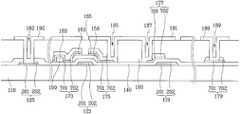
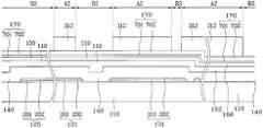
도 1은 본 발명의 제1 실시예에 따른 액정 표시 장치용 박막 트랜지스터 표시판이고, 도 2는 도 1에 도시한 박막 트랜지스터 표시판을 II-II' 선을 따라 잘라 도시한 단면도이다.1 is a thin film transistor array panel for a liquid crystal display according to a first exemplary embodiment of the present invention, and FIG. 2 is a cross-sectional view of the thin film transistor array panel shown in FIG. 1 taken along the line II-II '.
절연 기판(110) 위에 주로 가로 방향으로 뻗어 있는 복수의 게이트선(121)이 형성되어 있다. 게이트선(121)은 다른 물질과 접촉 특성이 우수한 크롬 또는 몰리브덴 또는 몰리브덴 합금 또는 탄탈륨 또는 티타늄 등으로 이루어진 하부 도전막(201)과 낮은 비저항을 가지는 알루미늄 또는 알루미늄 합금의 도전 물질로 이루어진 상부 도전막(202)으로 이루어져 있다. 게이트선(121)은 박막 트랜지스터의 게이트 전극(123)을 포함한다. 이때, 다른 부부보다 넓은 폭을 가지는 게이트선(121)의 일부는 이후에 형성되는 화소 전극(191)과 연결되어 있는 유지 축전기용 도전체 패턴(177)과 중첩되어 유지 축전기를 이루며, 여기서의 유지 용량이 충분하지 않은 경우에는 게이트 배선(121, 123, 125)으로부터 분리되어 있는 유지 배선을 추가될 수 있다.A plurality of
본 발명의 다른 실시예에 따르며, 액정 축전기의 전하 보존 능력을 향상시키는 유지 축전기의 한 전극을 이루는 복수의 유지 전극이 기판(110) 위에 형성되어 있다. 유지 전극은 기준 전압 또는 공통 전극 전압 따위의 미리 정해진 전압을 외부로부터 인가 받는다. 이때 기준 전압은 또한 다른 표시판의 기준 전극에도 인가 된다.In accordance with another embodiment of the present invention, a plurality of sustain electrodes forming one electrode of a sustain capacitor which improves the charge retention capability of the liquid crystal capacitor are formed on the
기판(110) 위에는 질화 규소(SiNx) 따위로 이루어진 게이트 절연막(140)이 게이트선(121)을 덮고 있다.On the
게이트 전극(123)의 게이트 절연막(140) 상부에는 비정질 규소 등으로 이루어진 반도체층(150)이 형성되어 있으며, 반도체층(150)의 상부에는 실리사이드 또는 n형 불순물이 고농도로 도핑되어 있는 n+ 수소화 비정질 규소 따위의 물질로 만들어진 저항 접촉 부재(163, 165)가 각각 형성되어 있다.A
저항 접촉층(163, 1653) 및 게이트 절연막(140) 위에는 알루미늄(Al) 또는 알루미늄 합금(Al alloy), 몰리브덴(Mo) 또는 몰리브덴-텅스텐(MoW) 합금, 크롬(Cr), 탄탈륨(Ta), 티타늄(Ti) 등의 금속 또는 도전체로 이루어진 데이터선(171) 및 드레인 전극(175)이 형성되어 있다. 데이터선(171)은 주로 세로 방향으로 뻗어 게이트선(121)과 교차하고 있으며, 데이터선(171)으로부터 뻗은 복수의 가지는 박막 트랜지스터의 소스 전극(173)을 이른다. 한 쌍의 소스 전극(173)과 드레인 전극(175)은 한 쌍의 저항성 접촉 부재(163, 165) 상부에 적어도 위치하며, 서로 분리되어 있으며 게이트 전극(123)에 대하여 서로 반대쪽에 위치한다. 데이터선(171)과 동일한 층에는 이후의 화소 전극(191)과 전기적으로 연결되어 있으며 앞에서 설명한 바와 같이 게이트선(121)과 중첩하는 유지 축전기용 도전체 패턴(177)이 형성되어 있다. 이때, 데이터선(171), 드레인 전극(175) 및 유지 축전기용 도전체(177)는 30-80° 범위의 경사각을 가지는 테이퍼 구조를 취할 수 있다.On the
데이터 배선(171) 및 드레인 전극(175)은 알루미늄 또는 알루미늄 합금의 단일막으로 형성하는 것이 바람직하지만, 이중층이상으로 형성될 수도 있다. 이중층 이상으로 형성하는 경우에는 한 층은 저항이 작은 물질로 형성하고 다른 층은 다른 물질, 특히 IZO 또는 ITO와 낮은 접촉 저항을 가지는 물질로 만드는 것이 바람직하다. 그 예로는 Al(또는 Al 합금)/Cr 또는 Al(또는 Al 합금)/Mo(또는 Mo 합금) 등을 들 수 있으며, 본 발명의 실시예에서 데이터선(171) 및 드레인 전극(175)은 크롬의 하부 도전막(701)과 알루미늄-네오디뮴 합금의 상부 도전막(702)의 이중막으로 이루어져 있다.The
데이터 배선(171), 드레인 전극(175) 및 유지 축전기용 도전체(177) 및 이들이 가리지 않는 반도체층(150) 상부에는 질화 규소로 이루어진 보호막(180)이 형성되어 있다.The
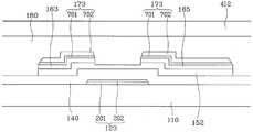
보호막(180)에는 드레인 전극(175) 및 데이터선의 끝 부분(179)를 각각 드러내는 접촉 구멍(185, 189)이 형성되어 있으며, 게이트 절연막(140)과 함께 게이트선의 끝 부분(125)를 드러내는 접촉 구멍(182)이 형성되어 있다. 여기서, 접촉 구멍(185)은 드레인 전극(175)의 경계선이 드러나도록 형성되어 있어, 드레인 전극(179)에 인접한 게이트 절연막(140) 일부도 접촉 구멍(185)을 통하여 드러나 있다. 드레인 전극(175)을 드러내는 접촉 구멍(185)은 10㎛×10㎛를 넘지 않으며 4㎛×4㎛ 이상인 것이 바람직하다. 또한, 게이트선 및 데이터선 각각의 끝 부분(125, 179)을 드러내는 접촉 구멍(182, 189)도 패드의 경계선이 드러나도록 형 성될 수 있으며 이에 대해서는 제2 실시예를 통하여 구체적으로 설명하기로 하며, 접촉부의 접촉 저항을 최소화하기 위해 접촉 구멍(185)보다 크게 형성하는 것이 바람직하다.In the
보호막(180) 위에는 투명한 도전 물질인 ITO 또는 IZO로 이루어진 화소 전극(191)이 형성되어 있다. 화소 전극(191)은 접촉 구멍(185)을 통하여 드레인 전극(175)과 전기적으로 연결되어 있는데, 화소 전극(191)은 접촉 구멍(185)에서 드러난 드레인 전극(175)의 하부막(701)과 충분히 접촉하고 있다. 이러한 본 발명의 실시예에 따른 구조에서는 화소 전극(191)은 드레인 전극(175)의 하부막(701)과 접촉하고 있어 화소 전극(191)과 드레인 전극(175)이 접촉하는 접촉부의 접촉 저항을 최소화할 수 있으며, 또한 드레인 전극(175)의 하부에서 언더 컷이 없어 접촉부에서 화소 전극(191)은 단선되지 않으며, 이를 통하여 접촉부의 프로파일을 양호하게 유도할 수 있다. 물론 화소 전극(191)과 유지 축전기용 도전체(177)가 접촉하는 접촉부에서도 화소 전극(191)과 드레인 전극(175)이 접촉하는 접촉부와 동일한 구조를 가진다.The
또한, 보호막(180) 위에는 접촉 구멍(182, 189)을 통하여 각각 게이트선의 끝 부분(125) 및 데이터선의 끝 부분(179)와 연결되어 있는 게이트 접촉 보조 부재(192) 및 데이터 접촉 보조 부재(199)가 형성되어 있다.In addition, on the
그러면, 이러한 본 발명의 제1 실시예에 따른 액정 표시 장치용 박막 트랜지스터 표시판의 제조 방법에 대하여 도 1 및 도 2와 도 3a 내지 도 9를 참고로 하여 상세히 설명한다.Next, a method of manufacturing the thin film transistor array panel for a liquid crystal display according to the first exemplary embodiment of the present invention will be described in detail with reference to FIGS. 1 and 2 and FIGS. 3A to 9.
먼저, 도 3a 및 3b에 도시한 바와 같이, 기판(110) 위에 크롬의 하부 도전막(201)과 알루미늄 합금의 금속 중, 2 at%의 Nd를 포함하는 Al-Nd를 포함하는 표적을 이용하여 2,500Å 정도의 두께로 상부 도전막(202)을 차례로 스퍼터링(sputtering)으로 적층하고 패터닝하여 게이트선(121)을 20-80°범위의 경사각의 테이퍼 구조로 형성한다.First, as shown in FIGS. 3A and 3B, by using a target including Al-Nd containing 2 at% of Nd in the lower
다음, 도 4a 및 도 4b에 도시한 바와 같이, 질화 규소로 이루어진 게이트 절연막(140), 비정질 규소층(150), 도핑된 비정질 규소층(160)의 삼층막을 연속하여 적층하고 마스크를 이용한 패터닝 공정으로 비정질 규소층(150)과 도핑된 비정질 규소층(160)을 패터닝하여 게이트 전극(123)과 마주하는 게이트 절연막(140) 상부에 반도체층(150)을 형성하고 그 상부에 도핑된 규소층(160)을 남긴다. 여기서, 게이트 절연막(140)은 질화 규소를 250~1500℃ 온도 범위, 2,000∼5,000Å 정도의 두께로 적층하여 형성하는 것이 바람직하다.Next, as shown in FIGS. 4A and 4B, a three-layer film of a
다음, 도 5a 내지 도 5b에 도시한 바와 같이, 몰리브덴 또는 몰리브덴 합금 또는 크롬 등으로 이루어진 하부 도전막(701)을 500Å 정도의 두께로, 저저항을 가지는 알루미늄 또는 알루미늄 합금의 금속 중, 2 at%의 Nd를 포함하는 Al-Nd 합금의 표적을 이용하여 상부 도전막(702)을 150℃ 정도에서 2,500Å 정도의 두께로 스퍼터링(sputtering)을 통하여 차례로 적층한 후, 마스크를 이용한 사진 공정으로 패터닝하여 게이트선(121)과 교차하는 데이터선(171), 데이터선(171)과 분리되어 있으며 게이트 전극(123)을 중심으로 소스 전극(173)과 마주하는 드레인 전극(175) 및 게이트선(121)과 중첩하는 유지 축전기용 도전체(177)를 테이퍼 구조로 형성한 다. 여기서, 상부막(702) 및 하부막(701)은 모두 습식 식각으로 식각할 수 있으며, 상부막(702)은 습식 식각으로 하부막(701)은 건식 식각으로 식각할 수 있으며, 하부막(701)이 몰리브덴 또는 몰리브덴 합금막인 경우에는 상부막(702)과 하나의 식각 조건으로 패터닝할 수 있다.Next, as shown in FIGS. 5A to 5B, the lower
이어, 데이터선(171), 드레인 전극(175) 및 유지 축전기용 도전체(177)로 가리지 않는 도핑된 비정질 규소층(160)을 식각하여 게이트 전극(123)을 중심으로 양쪽으로 분리시켜 저항성 접촉 부재(163, 165)를 형성하는 한편, 양쪽의 저항성 접촉 부재(163, 165) 사이의 반도체층(150)을 노출시킨다. 이어, 노출된 반도체층(150)의 표면을 안정화시키기 위하여 산소 플라스마를 실시하는 것이 바람직하다.Subsequently, the doped
다음으로, 도 6에서 보는 바와 같이, 질화 규소와 같은 무기 절연막을 또는 낮은 유전율을 가지는 유기 절연막을 적층하여 보호막(180)을 형성하고, 그 상부에 감광막(210)을 스핑 코팅 방법으로 도포한다.Next, as shown in FIG. 6, an inorganic insulating film such as silicon nitride or an organic insulating film having a low dielectric constant is stacked to form a
그 후, 마스크를 통하여 감광막(210)에 빛을 조사한 후 현상하여 도 7b에 도시한 바와 같이, 감광막 패턴(212, 214)을 형성한다. 이때, 감광막 패턴(212, 214) 중에서 접촉부(C1), 즉 드레인 전극(175) 및 유지 축전기용 도전체(177)상부에 위치한 제1 부분(214)은 게이트 패드(125)에 대응하는 패드부(B1)를 제외한 기타부(A1)에 위치한 제2 부분(212)보다 얇은 두께를 가지며, 패드부(B1)의 감광막은 모두 제거한다. 이 때, 데이터선의 끝 부분(179) 상부에 위치하는 감광막은 패드부(B1)와 동일한 두께로 남길 수 있으나, 본 발명의 실시예에서는 접촉부(C1)와 동 일한 두께로 남긴다. 여기서, 접촉부(C1)에 남아 있는 감광막(214)의 두께와 기타부(A1)에 남아 있는 감광막(212)의 두께의 비는 후에 후술할 식각 공정에서의 공정 조건에 따라 조절하며, 제1 부분(214)의 두께는 보호막(180)보다 같거나 얇은 두께로 남기는 것이 바람직하다.Thereafter, the
이와 같이, 위치에 따라 감광막의 두께를 달리하는 방법으로 여러 가지가 있을 수 있으며, C1 영역의 빛 투과량을 조절하기 위하여 주로 슬릿(slit)이나 격자 형태의 패턴을 형성하거나 반투명막을 사용한다.As such, there may be various methods of varying the thickness of the photoresist layer according to the position. In order to control the light transmission amount of the C1 region, a slit or lattice-shaped pattern is mainly used or a translucent film is used.
이때, 슬릿 사이에 위치한 패턴의 선 폭이나 패턴 사이의 간격, 즉 슬릿의 폭은 노광시 사용하는 노광기의 분해능보다 작은 것이 바람직하며, 반투명막을 이용하는 경우에는 마스크를 제작할 때 투과율을 조절하기 위하여 다른 투과율을 가지는 박막을 이용하거나 두께가 다른 박막을 이용할 수 있다.In this case, the line width of the pattern located between the slits or the interval between the patterns, that is, the width of the slits, is preferably smaller than the resolution of the exposure machine used for exposure, and in the case of using a translucent film, the transmittance is different in order to control the transmittance when fabricating a mask. A thin film having a thickness or a thin film may be used.
이와 같은 마스크를 통하여 감광막에 빛을 조사하면 빛에 직접 노출되는 부분에서는 고분자들이 완전히 분해되며, 슬릿 패턴이나 반투명막이 형성되어 있는 부분에서는 빛의 조사량이 적으므로 고분자들은 완전 분해되지 않은 상태이며, 차광막으로 가려진 부분에서는 고분자가 거의 분해되지 않는다. 이어 감광막을 현상하면, 고분자 분자들이 분해되지 않은 부분만이 남고, 빛이 적게 조사된 중앙 부분에는 빛에 전혀 조사되지 않은 부분보다 얇은 두께의 감광막이 남길 수 있다. 이때, 노광 시간을 길게 하면 모든 분자들이 분해되므로 그렇게 되지 않도록 해야 한다.When the light is irradiated to the photosensitive film through such a mask, the polymers are completely decomposed at the part directly exposed to the light, and the polymers are not completely decomposed because the amount of light is small at the part where the slit pattern or the translucent film is formed. In the area covered by, the polymer is hardly decomposed. Subsequently, when the photoresist film is developed, only a portion where the polymer molecules are not decomposed is left, and a thin photoresist film may be left at a portion where the light is not irradiated at a portion less irradiated with light. In this case, if the exposure time is extended, all molecules are decomposed, so it should not be so.
이러한 얇은 두께의 감광막(214)은 리플로우가 가능한 물질로 이루어진 감광 막을 이용하고 빛이 완전히 투과할 수 있는 부분과 빛이 완전히 투과할 수 없는 부분으로 나뉘어진 통상적인 마스크로 노광한 다음 현상하고 리플로우시켜 감광막이 잔류하지 않는 부분으로 감광막의 일부를 흘러내리도록 함으로써 형성할 수도 있다.This
이어, 감광막 패턴(212, 214)을 식각 마스크로 하여 그 하부의 막인 보호막(180) 및 게이트 절연막(140)에 대한 식각을 진행한다. 이때, 패드부(B1)에서는 게이트 절연막(140)과 보호막(180)이 제거되어야 하고, 접촉부(C1)에서는 적어도 게이트 절연막(140)이 남아 있어야 한다.Subsequently, using the
우선, 도 8에서 보는 바와 같이, 감광막 패턴(212, 214)을 마스크로 하여 보호막(180) 또는 게이트 절연막(140)을 식각하는데, 이때, 패드부(B1)에서는 보호막(180)이 완전히 제거되어야 하며, 접촉부(C1)에서는 감광막의 일부가 잔류할 수도 있다. 이때, 식각은 건식 식각 방법을 적용하며, 보호막(180) 및 감광막(212, 214)에 대하여 실질적으로 동일한 식각비를 가지는 식각 조건으로 실시하는 것이 좋다. 이는 접촉 구멍(185, 187)을 도 1 및 도 2에서 보는 바와 같이 드레인 전극(175) 및 유지 축전기용 도전체 패턴(177)의 경계선이 드러나도록 형성하더라도 이후의 식각 공정에서 드레인 전극(175) 및 유지 축전기용 도전체 패턴(177) 하부에 게이트 절연막(140)을 용이하게 남길 수 있도록 하기 위함이다. 패드부(B1)에서 남은 게이트 절연막(140)의 두께는 보호막(180)보다 얇은 것이 바람직하며, 이는 이후의 식각 공정에서 패드부(B1)에서 게이트선의 끝 부분(125)을 드러내기 위해 게이트 절연막(140)을 완전히 제거하더라도 접촉부(C1)에서는 보호 막(180)을 제거하고 게이트 절연막(140)이 식각되지 않도록 하여 접촉부(C1)의 드레인 전극(175) 및 유지 축전기용 도전체(177) 하부에서 언더 컷이 발생하지 않도록 하기 위함이다. 도면에서 보는 바와 같이 패드부(B1)에서는 게이트 절연막(140) 일부가 식각될 수 있다. 이어, 애싱 공정을 통하여 접촉부(C1)에서 잔류하는 감광막의 제1 부분(214)을 완전히 제거하여 접촉부(C1)에서 드레인 전극(175) 상부에 위치하는 보호막(180)을 드러낸다.First, as shown in FIG. 8, the
이어, 도 9에서 보는 바와 같이, 남은 감광막의 제2 부분(212)을 식각 마스크로 사용하여 드러난 접촉부(C1) 및 패드부(B1)에서 보호막(180) 및 게이트 절연막(140)을 제거하여 드레인 전극(175) 및 유지 축전기용 도전체(177) 및 게이트선의 끝 부분(125)과 데이터선의 끝 부분(179)을 드러내는 접촉 구멍(185, 187, 182, 189)을 완성한다. 이때, 식각은 건식 식각으로 사용하며, 게이트 절연막(140)과 보호막(180)에 대하여 실질적으로 동일한 식각비를 가지는 식각 조건으로 실시한다. 이렇게 하면, 패드부(B1)에서 게이트선의 끝 부분(125) 상부의 게이트 절연막(140)은 접촉부(C)의 보호막(180)보다 얇은 두께를 가지고 있기 때문에, 접촉부(C1)에서 보호막(180)만을 제거하여 드레인 전극(175) 및 유지 축전기용 도전체(177)가 드러날 때, 패드부(B1)에서는 게이트 절연막(140)이 완전히 제거되어 게이트선 끝 부분(125)을 접촉 구멍(182)을 완성할 수 있으며, 접촉부(C1)에서는 게이트 절연막(140)을 완전히 제거되는 것을 방지할 수 있다. 이어, 접촉 구멍(182, 185, 187)을 통하여 드러난 알루미늄 합금의 상부막(202, 702)을 제거한다. 이는 드레인 전극(175) 또는 게이트선 및 데이터선 끝 부분(125, 179)과 이후에 형성되 는 ITO 및 IZO와의 접촉 저항을 최소화하기 위함이다.Subsequently, as shown in FIG. 9, the
다음, 마지막으로 도 1 및 2에 도시한 바와 같이, IZO 또는 ITO막을 스퍼터링으로 적층하고 마스크를 이용한 패터닝을 실시하여 접촉 구멍(185, 187)을 통하여 드레인 전극(175) 및 유지 축전기용 도전체(187)와 연결되는 화소 전극(191)과 접촉 구멍(182, 189)을 통하여 게이트선의 끝 부분(125) 및 데이터선의 끝 부분(179)과 각각 연결되는 게이트 접촉 보조 부재(192) 및 데이터 접촉 보조 부재(199)를 각각 형성한다. 이때, 화소 전극(191)은 드레인 전극(175) 및 유지 축전기용 도전체(177)의 하부에서 언더 컷이 발생하지 않아 단선되지 않아 접촉부의 프로파일을 완만하게 형성할 수 있으며, 접촉부에서 IZO 또는 ITO막과 낮은 접촉 저항을 가지는 하부막(701)과 충분히 접하고 있어 접촉부의 접촉 저항을 최소화할 수 있다.Next, as shown in FIGS. 1 and 2, the IZO or ITO film is laminated by sputtering and patterned using a mask to conduct
이러한 본 발명의 실시예에 따른 박막 트랜지스터 표시판의 구조는 게이트선(121) 및 데이터선(171)이 저저항을 가지는 알루미늄 또는 알루미늄 합금의 도전막을 포함하고 있는 동시에 접촉부 특히 데이터 배선과 화소 전극(191)의 접촉 저항을 최소화할 수 있어 대화면 고정세의 액정 표시 장치에 적용할 수 있다.The structure of the thin film transistor array panel according to the exemplary embodiment of the present invention includes a conductive film of aluminum or aluminum alloy in which the
이러한 방법은 앞에서 설명한 바와 같이, 5매의 마스크를 이용하는 제조 방법에 적용할 수 있지만, 4매 마스크를 이용하는 액정 표시 장치용 박막 트랜지스터 표시판의 제조 방법에서도 동일하게 적용할 수 있다. 이에 대하여 도면을 참조하여 상세하게 설명하기로 한다.As described above, this method can be applied to a manufacturing method using five masks, but the same method can be applied to a manufacturing method of a thin film transistor array panel for a liquid crystal display device using four masks. This will be described in detail with reference to the drawings.
먼저, 도 10 내지 도 12를 참고로 하여 본 발명의 실시예에 따른 4매 마스크 를 이용하여 완성된 액정 표시 장치용 박막 트랜지스터 표시판의 단위 화소 구조에 대하여 상세히 설명한다.First, a unit pixel structure of a thin film transistor array panel for a liquid crystal display device completed using four masks according to an exemplary embodiment of the present invention will be described in detail with reference to FIGS. 10 to 12.
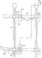
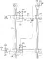
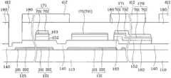
도 10은 본 발명의 제2 실시예에 따른 액정 표시 장치용 박막 트랜지스터 표시판의 배치도이고, 도 11 및 도 12는 각각 도 10에 도시한 박막 트랜지스터 표시판을 XI-XI' 선 및 XII-XII' 선을 따라 잘라 도시한 단면도이다.10 is a layout view of a thin film transistor array panel for a liquid crystal display according to a second exemplary embodiment of the present invention, and FIGS. 11 and 12 are lines XI-XI ′ and XII-XII ′, respectively, of the thin film transistor array panel illustrated in FIG. 10. A cross-sectional view taken along the line.
먼저, 절연 기판(110) 위에 제1 실시예와 동일하게 알루미늄 또는 알루미늄 합금의 저저항 도전 물질로 이루어진 게이트선(121)이 형성되어 있다. 그리고, 기판(110) 상부에는 게이트선(121)과 평행하며 다른 표시판에 형성되어 있는 공통 전극(도시하지 않음)에 입력되는 공통 전극 전압 따위의 전압을 외부로부터 인가받는 유지 전극선(131)이 형성되어 있다. 유지 전극선(131)은 후술할 화소 전극(191)과 연결된 드레인 전극(175)과 중첩되어 화소의 전하 보존 능력을 향상시키는 유지 축전기를 이루며, 후술할 화소 전극(191)과 게이트선(121)의 중첩으로 발생하는 유지 용량이 충분할 경우 형성하지 않을 수도 있다.First, a
게이트선(121) 및 유지 전극선(131)은 마찬가지로 알루미늄 또는 알루미늄 합금으로 이루어진 단일층으로 형성될 수도 있지만, IZO 또는 ITO와 낮은 접촉 저항을 가지는 크롬 또는 몰리브덴 또는 몰리브덴 합금 또는 탄탈륨 또는 티타늄으로 이루어진 하부막(201)과 알루미늄 또는 알루미늄 합금으로 이루어진 상부막(202)을 포함하는 이중막으로 형성되어 있다.The
게이트선(121) 및 유지 전극선(131) 위에는 질화 규소(SiNx) 따위로 이루어 진 게이트 절연막(140)이 형성되어 게이트선(121) 및 유지 전극선(131)을 덮고 있다.A
게이트 절연막(140) 위에는 수소화 비정질 규소(hydrogenated amorphous silicon) 따위의 반도체(152)가 형성되어 있으며, 반도체(152) 위에는 인(P) 따위의 n형 불순물로 고농도로 도핑되어 있는 비정질 규소 따위로 이루어진 저항성 접촉 부재(ohmic contact layer)(163, 165)가 형성되어 있다.A
저항성 접촉 부재(163, 165) 위에는 저저항을 가지는 알루미늄 또는 알루미늄 합금의 도전 물질로 이루어진 도전막을 포함하는 데이터선(171) 및 드레인 전극(175)이 형성되어 있다. 데이터선(171)은 게이트 전극(123) 상부에 위치하는 소스 전극(173)을 포함한다. 이때, 드레인 전극(175)은 데이터선(171)과 분리되어 있으며 게이트 전극(123) 또는 박막 트랜지스터의 채널부에 대하여 소스 전극(173)의 반대쪽에 위치하며 유지 전극선(131) 상부까지 연장되어 있다.On the
데이터선(171), 드레인 전극(175)도 게이트선(121)과 마찬가지로 알루미늄 또는 알루미늄 합금의 금속으로 이루어진 단일층으로 형성될 수도 있지만, 제1 실시예와 동일하게 크롬 또는 몰리브덴 또는 몰리브덴 합금 또는 탄탈륨 또는 티타늄으로 이루어진 하부막(701)과 알루미늄 또는 알루미늄 합금으로 이루어진 상부막(702)을 포함하는 이중막으로 형성되어 있다.The
저항성 접촉 부재(163, 165)는 그 하부의 반도체(152)와 그 상부의 데이터선(171) 및 드레인 전극(175)의 접촉 저항을 낮추어 주는 역할을 하며, 데이터선(171) 및 드레인 전극(175)과 실질적으로 동일한 형태를 가진다.The
한편, 반도체(152)는 박막 트랜지스터의 채널부인 소스 전극(173)과 드레인 전극(175) 사이를 제외하면 데이터선(171) 및 드레인 전극(175) 및 저항성 접촉 부재(163, 165)와 실질적으로 동일한 모양을 하고 있다. 즉, 박막 트랜지스터의 소스 전극(173)과 드레인 전극(175)이 분리되어 있고 한 쌍은 저항성 접촉 부재(163, 165)도 분리되어 있으나, 박막 트랜지스터용 반도체(152)는 이곳에서 끊어지지 않고 연결되어 박막 트랜지스터의 채널을 생성한다.The
데이터선(171) 및 드레인 전극(175) 위에는 질화 규소로 이루어진 보호막(180)이 형성되어 있다.A
보호막(180)은 드레인 전극(175) 및 데이터선의 끝 부분(179)을 드러내는 접촉 구멍(185, 189)을 가지고 있으며, 또한 게이트 절연막(140)과 함께 게이트선의 끝 부분(125)을 드러내는 접촉 구멍(182)을 가지고 있다. 이때, 접촉 구멍(182, 185, 189) 모두는 게이트선의 끝 부분(125), 드레인 전극(175), 데이터선의 끝 부분(179)의 경계선이 드러나도록 형성되어 있으며, 접촉 구멍(182, 185, 189)에서는 IZO 또는 ITO와 낮은 접촉 저항을 가지는 하부막(201, 701)이 드러나 있다.The
보호막(180) 위에는 박막 트랜지스터로부터 화상 신호를 받아 상판의 전극과 함께 전기장을 생성하는 화소 전극(191)이 형성되어 있다. 화소 전극(191)은 접촉 구멍(185)을 통하여 드레인 전극(175)과 물리적·전기적으로 연결되어 화상 신호를 전달받는다. 화소 전극(191)은 또한 이웃하는 게이트선(121) 및 데이터선(171)과 중첩되어 개구율을 높이고 있으나, 중첩되지 않을 수도 있다. 한편, 게이트선의 끝 부분(125) 및 데이터선의 끝 부분(179) 위에는 접촉 구멍(182, 189)을 통하여 각각 이들과 연결되는 게이트 접촉 보조 부재(192) 및 데이터 접촉 보조 부재(199)가 형성되어 있으며, 이들은 게이트선 및 데이터선 각각의 끝 부분(125, 179)과 외부 회로 장치와의 접착성을 보완하고 패드를 보호하는 역할을 하는 것으로 필수적인 것은 아니며, 이들의 적용 여부는 선택적이다. 여기서도, 제1 실시예와 동일하게 접촉부 또는 패드부에서 IZO막(191, 192, 199)은 게이트선의 끝 부분(125), 드레인 전극(175), 데이터선의 끝 부분(179)의 하부막(201, 701)과 접촉되어 있다. 이때, 접촉 구멍(185, 189)은 드레인 전극(175) 및 데이터선의 끝 부분(179)의 경계선이 드러나 있어도, 드레인 전극(175) 및 데이터선의 끝 부분(179)의 주변에는 게이트 절연막(140)이 남아 있어 화소 전극(191) 및 데이터 접촉 보조 부재(199)는 접촉 구멍(185, 189)에서 단선되지 않고, 완만한 프로파일을 가진다.A
여기에서는 화소 전극(191)의 재료의 예로 투명한 IZO를 들었으나, 투명한 도전성 폴리머(polymer) 등으로 형성할 수도 있으며, 반사형 액정 표시 장치의 경우 불투명한 도전 물질을 사용하여도 무방하다.Although the transparent IZO is mentioned as an example of the material of the
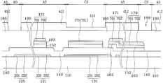
그러면, 도 10 내지 도 12의 구조를 가지는 액정 표시 장치용 박막 트랜지스터 표시판을 4매 마스크를 이용하여 제조하는 방법에 대하여 상세하게 도 10 내지 도 12와 도 13a 내지 도 22c를 참조하여 설명하기로 한다.Next, a method of manufacturing a thin film transistor array panel for a liquid crystal display device having the structure of FIGS. 10 to 12 using four masks will be described in detail with reference to FIGS. 10 to 12 and FIGS. 13A to 22C. .
먼저, 도 13a 내지 13c에 도시한 바와 같이, ITO 또는 IZO와 낮은 접촉 저항을 가지는 몰리브덴 또는 몰리브덴 합금 또는 크롬 등으로 이루어진 하부 도전막(201)과 낮은 비저항을 가지는 알루미늄 또는 알루미늄 합금 중, 2 at%의 Nd를 포함하는 Al-Nd 합금의 표적을 스퍼터링하여 적층한 상부 도전막(202)을 차례로 형성한 후, 1 마스크를 이용한 사진 식각 공정으로 기판(110) 위에 게이트선(121) 및 유지 전극선(131)을 테이퍼 구조로 형성한다. First, as shown in FIGS. 13A to 13C, 2 at% of the lower
다음, 도 14a 및 14b에 도시한 바와 같이, 질화 규소로 이루어진 게이트 절연막(140), 비정질 규소층(150), 도핑된 비정질 규소층(160)을 화학 기상 증착법을 이용하여 각각 1,500 Å 내지 5,000 Å, 500 Å 내지 2,000 Å, 11500 Å 내지 600 Å의 두께로 연속 증착하고, 이어 크롬 또는 몰리브덴 또는 몰리브덴 합금으로 이루어진 하부 도전막(701)과 낮은 비저항을 가지는 알루미늄 또는 알루미늄 합금으로 이루어진 하부막(701)을 포함하는 도전체층(170)을 스퍼터링 등의 방법으로 1,500 Å 내지 3,000 Å의 두께로 증착한 다음 그 위에 감광막(310)을 1 μm 내지 2 μm의 두께로 도포한다.Next, as shown in FIGS. 14A and 14B, the
그 후, 제2 마스크를 통하여 감광막(310)에 빛을 조사한 후 현상하여 도 15b 및 15c에 도시한 바와 같이, 감광막 패턴(312, 314)을 형성한다. 이때, 감광막 패턴(312, 314) 중에서 박막 트랜지스터의 채널부(C2), 즉 소스 전극(173)과 드레인 전극(175) 사이에 위치한 제1 부분(314)은 배선부(A2), 즉 데이터선(171) 및 드레인 전극(175)이 형성될 부분에 위치한 제2 부분(312)보다 두께가 작게 되도록 하며, 기타 부분(B2)의 감광막은 모두 제거한다. 이 때, 채널부(C2)에 남아 있는 감광막(314)의 두께와 배선부(A2)에 남아 있는 감광막(312)의 두께의 비는 후에 후술할 식각 공정에서의 공정 조건에 따라 다르게 하여야 하되, 제1 부분(314)의 두께를 제2 부분(312)의 두께의 1/2 이하로 하는 것이 바람직하며, 예를 들면, 4,000 Å 이하인 것이 좋다.Thereafter, the
이와 같이, 위치에 따라 감광막의 두께를 달리하는 방법은 제1 실시예와 동일하다.As such, the method of varying the thickness of the photosensitive film according to the position is the same as that of the first embodiment.
이어, 감광막 패턴(314) 및 그 하부의 막들, 즉 도전체층(170), 도핑된 비정질 규소층(160) 및 비정질 규소층(150)에 대한 식각을 진행한다. 이때, 배선부(A2)에는 데이터선, 드레인 전극 및 그 하부의 막들이 그대로 남아 있고, 채널부(C2)에는 비정질 규소의 반도체만 남아 있어야 하며, 나머지 부분(B2)에는 위의 3개 층(170, 160, 150)이 모두 제거되어 게이트 절연막(140)이 드러나야 한다.Subsequently, etching is performed on the
먼저, 도 16a 및 16b에 도시한 것처럼, 기타 부분(B2)의 노출되어 있는 도전체층(170)을 제거하여 그 하부의 도핑된 비정질 규소층(160)을 노출시킨다. 이 과정에서는 건식 식각 또는 습식 식각 방법을 모두 사용할 수 있으며, 이때 도전체층(170)은 식각되고 감광막 패턴(312, 314)은 거의 식각되지 않는 조건하에서 행하는 것이 좋다. 그러나, 건식 식각의 경우 도전체층(170)만을 식각하고 감광막 패턴(312, 314)은 식각되지 않는 조건을 찾기가 어려우므로 감광막 패턴(312, 314)도 함께 식각되는 조건하에서 행할 수 있다. 이 경우에는 습식 식각의 경우보다 제1 부분(314)의 두께를 두껍게 하여 이 과정에서 제1 부분(314)이 제거되어 하부의 도전체층(170)이 드러나는 일이 생기지 않도록 한다.First, as shown in FIGS. 16A and 16B, the exposed
도전체층(170)의 도전막 중 Mo 또는 MoW 합금, Al 또는 Al 합금, Ta 중 하나를 포함하는 도전막은 건식 식각이나 습식 식각 중 어느 것이라도 가능하다. 그러나 Cr은 건식 식각 방법으로는 잘 제거되지 않기 때문에 하부막(701)이 Cr이라면 습식 식각만을 이용하는 것이 좋다. 하부막(701)이 Cr인 습식 식각의 경우에는 식 각액으로 CeNHO3을 사용할 수 있고, 하부막(701)이 Mo나 MoW인 건식 식각의 경우의 식각 기체로는 CF4와 HCl의 혼합 기체나 CF4와 O2의 혼합 기체를 사용할 수 있으며 후자의 경우 감광막에 대한 식각비도 거의 비슷하다.The conductive film including Mo or MoW alloy, Al or Al alloy, or Ta among the conductive films of the
이렇게 하면, 도 16a 및 도 16b에 나타낸 것처럼, 채널부(C2) 및 배선부(B2)의 도전체층, 즉 배선용 도전체(178)만이 남고 기타 부분(B2)의 도전체층(170)은 모두 제거되어 그 하부의 도핑된 비정질 규소층(160)이 드러난다. 이때 남은 도전체(178)는 소스 및 드레인 전극(173, 175)이 분리되지 않고 연결되어 있는 점을 제외하면 데이터선(171) 및 드레인 전극(175)의 형태와 동일하다. 또한 건식 식각을 사용한 경우 감광막 패턴(312, 314)도 어느 정도의 두께로 식각된다.In this way, as shown in Figs. 16A and 16B, only the conductor layer of the channel portion C2 and the wiring portion B2, that is, the
이어, 도 17a 및 17b에 도시한 바와 같이, 기타 부분(B2)의 노출된 도핑된 비정질 규소층(160) 및 그 하부의 비정질 규소층(150)을 감광막의 제1 부분(314)과 함께 건식 식각 방법으로 동시에 제거한다. 이 때의 식각은 감광막 패턴(312, 314)과 도핑된 비정질 규소층(160) 및 비정질 규소층(150)(비정질 규소층과 도핑된 비정질 규소층은 식각 선택성이 거의 없음)이 동시에 식각되며 게이트 절연막(140)은 식각되지 않는 조건하에서 행하여야 하며, 특히 감광막 패턴(312, 314)과 비정질 규소층(150)에 대한 식각비가 거의 실질적으로 동일한 조건으로 식각하는 것이 바람직하다. 예를 들어, SF6과 HCl의 혼합 기체나, SF6과 O2의 혼합 기체를 사용하면 거의 동일한 두께로 두 막을 식각할 수 있다. 감광막 패턴(312, 314)과 비정질 규소층(150)에 대한 식각비가 동일한 경우 제1 부분(314)의 두께는 비정질 규소층(150)과 도핑된 비정질 규소층(160)의 두께를 합한 것과 같거나 그보다 작아야 한다.Then, as shown in FIGS. 17A and 17B, the exposed doped
이렇게 하면, 도 17a 및 17b에 나타낸 바와 같이, 채널부(C2)의 제1 부분(314)이 제거되어 소스/드레인용 도전체(178)이 드러나고, 기타 부분(B2)의 도핑된 비정질 규소층(160) 및 비정질 규소층(150)이 제거되어 그 하부의 게이트 절연막(140)이 드러난다. 한편, 배선부(A2)의 제2 부분(312) 역시 식각되므로 두께가 얇아진다. 또한, 이 단계에서 비정질 규소층의 반도체(152)가 완성된다. 도면 부호 168은 각각 소스/드레인용 도전체(178) 하부의 도핑된 비정질 규소층을 가리킨다.This removes the
이어 애싱(ashing)을 통하여 채널부(C2)의 소스/드레인용 도전체(178) 표면에 남아 있는 감광막 찌꺼기를 제거한다.Subsequently, ashing of the photoresist film remaining on the surface of the source /
다음, 도 18a 및 18b에 도시한 바와 같이 채널부(C2)의 소스/드레인용 도전체(178) 및 그 하부의 도핑된 비정질 규소층(168)을 식각하여 제거한다. 이 때, 식각은 소스/드레인용 도전체(178)와 비정질 규소층(168) 모두에 대하여 건식 식각만으로 진행할 수도 있으며, 소스/드레인용 도전체(178)에 대해서는 습식 식각으로, 도핑된 비정질 규소층(168)에 대해서는 건식 식각으로 행할 수도 있다. 전자의 경우 소스/드레인용 도전체(178)와 도핑된 비정질 규소층(168)의 식각 선택비가 큰 조건하에서 식각을 행하는 것이 바람직하며, 이는 식각 선택비가 크지 않을 경우 식각 종점을 찾기가 어려워 채널부(C2)에 남는 반도체(152)의 두께를 조절하기 가 쉽지 않기 때문이다. 예를 들면, SF6과 O2의 혼합 기체를 사용하여 소스/드레인용 도전체(178)을 식각하는 것을 들 수 있다. 습식 식각과 건식 식각을 번갈아 하는 후자의 경우에는 습식 식각되는 소스/드레인용 도전체(178)의 측면은 식각되지만, 건식 식각되는 도핑된 비정질 규소층(168)은 거의 식각되지 않으므로 계단 모양으로 만들어진다. 도핑된 비정질 규소층(168) 및 반도체(152)를 식각할 때 사용하는 식각 기체의 예로는 앞에서 언급한 CF4와 HCl의 혼합 기체나 CF4와 O2의 혼합 기체를 들 수 있으며, CF4와 O2를 사용하면 균일한 두께로 반도체(152)을 남길 수 있다. 이때, 도 18b에 도시한 것처럼 반도체(152)의 일부가 제거되어 두께가 작아질 수도 있으며 감광막 패턴의 제2 부분(312)도 이때 어느 정도의 두께로 식각된다. 이때의 식각은 게이트 절연막(140)이 식각되지 않는 조건으로 행하여야 하며, 제2 부분(312)이 식각되어 그 하부의 데이터선(171) 및 드레인 전극(175)이 드러나는 일이 없도록 감광막 패턴이 두꺼운 것이 바람직함은 물론이다.Next, as illustrated in FIGS. 18A and 18B, the source /
이렇게 하면, 도 15a, 18a 및 18b에서 보는 바와 같이, 데이터선(171)과 드레인 전극(175)이 분리되면서 데이터선(171) 및 드레인 전극(175)과 그 하부의 저항성 접촉 부재(163, 165)이 완성된다.In this case, as shown in FIGS. 15A, 18A, and 18B, the
마지막으로 데이터 배선부(A2)에 남아 있는 감광막 제2 부분(312)을 제거한다. 그러나, 제2 부분(312)의 제거는 채널부(C2) 소스/드레인용 도전체(178)를 제거한 후 그 밑의 도핑된 비정질 규소층(168)을 제거하기 전에 이루어질 수도 있다.Finally, the photosensitive film
앞에서 설명한 것처럼, 습식 식각과 건식 식각을 교대로 하거나 건식 식각만 을 사용할 수 있다. 후자의 경우에는 한 종류의 식각만을 사용하므로 공정이 비교적 간편하지만, 알맞은 식각 조건을 찾기가 어렵다. 반면, 전자의 경우에는 식각 조건을 찾기가 비교적 쉬우나 공정이 후자에 비하여 번거로운 점이 있다.As mentioned earlier, wet and dry etching can be alternately used, or only dry etching can be used. In the latter case, since only one type of etching is used, the process is relatively easy, but it is difficult to find a suitable etching condition. On the other hand, in the former case, the etching conditions are relatively easy to find, but the process is more cumbersome than the latter.
이와 같이 하여 데이터선(171) 및 드레인 전극(175)을 형성한 후, 남은 감광막 패턴(314)을 제거하고, 도 19a 및 19b에 도시한 바와 같이 제1 실시예와 같이 질화 규소를 CVD 방법으로 증착하거나 낮은 유전율을 가지는 유기 절연막을 적층하여 보호막(180)을 형성한다. 이어, 그 상부에 감광막(410)을 스핑 코팅 방법으로 도포한 후, 마스크를 통하여 감광막(410)에 빛을 조사한 후 현상하여 도 19b 및 도 19c에서 보는 바와 같이 제1 실시예와 같이 감광막 패턴(412, 414)을 형성한다. 이때, 감광막 패턴(412, 414) 중에서 접촉부(C3), 즉 드레인 전극(175)상부에 위치한 제1 부분(414)은 게이트선의 끝 부분(125)에 대응하는 패드부(B3)를 제외한 기타부(A3)에 위치한 제2 부분(412)보다 얇은 두께를 가지며, 패드부(B3)의 감광막은 모두 제거한다. 이 때, 데이터선의 끝 부분(179)의 상부에 위치하는 감과막의 제1 부분(414)은 패드부(B3)와 실질적으로 동일한 두께로 남길 수 있으나, 본 발명의 실시예에서는 접촉부(C3)와 실질적으로 동일한 두께로 남긴다. 여기서, 접촉부(C3)에 남아 있는 감광막(414)은 보호막(180)보다 같거나 얇은 두께로 남기는 것이 바람직하다.After the
이때, 감광막 패턴(412, 414)을 식각 마스크로 하여 그 하부의 막인 보호막(180) 및 게이트 절연막(140)에 대한 식각을 진행한다. 이때, 패드부(B3)에서는 게이트 절연막(140)과 보호막(180)이 제거되어야 하고, 접촉부(C3)에서는 적 어도 게이트 절연막(140)이 남아 있어야 한다.At this time, the
우선, 도 20a 및 도 20b에서 보는 바와 같이 감광막 패턴(412, 414)을 마스크로 하여 보호막(180) 또는 게이트 절연막(140)을 식각하는데, 이때, 패드부(B3)에서는 보호막(180)이 완전히 제거되어야 하며, 접촉부(C3)에서는 감광막의 일부가 잔류할 수도 있다. 이때, 식각 조건은 제1 실시예와 동일하며, 패드부(B3)에서 남은 게이트 절연막(140)의 두께는 보호막(180)보다 얇은 것이 바람직하며, 이는 앞에서 설명한 바와 같이 드레인 전극(175) 하부에서 언더 컷이 발생하지 않도록 하기 위함이다. 도면에서 보는 바와 같이 패드부(B3)에서는 게이트 절연막(140) 일부가 식각될 수 있다. 이어, 애싱 공정을 통하여 접촉부(C3)에서 잔류하는 감광막의 제1 부분(414)을 완전히 제거하여 접촉부(C3)에서 드레인 전극(175) 상부에 위치하는 보호막(180)을 드러낸다.First, as shown in FIGS. 20A and 20B, the
이어, 도 21a 및 도 21b에서 보는 바와 같이, 남은 감광막의 제2 부분(412)을 식각 마스크로 사용하여 드러난 접촉부(C3)에서 보호막(180)을 제거하여 드레인 전극(175)을 드러내는 접촉 구멍(185)을 완성한다. 이때, 식각은 건식 식각으로 사용하며, 게이트 절연막(140)과 보호막(180)에 대하여 실질적으로 동일한 식각비를 가지는 식각 조건으로 실시한다. 이렇게 하면, 패드부(B3)에서 게이트선의 끝 부분(125) 상부의 게이트 절연막(140)은 접촉부(C3)의 보호막(180)보다 얇은 두께를 가지고 있기 때문에, 패드부(B3)에서는 게이트 절연막(140)이 완전히 제거되어 게이트선의 끝 부분(125)을 접촉 구멍(182)을 완성할 수 있으며, 접촉부(C3)에서는 게이트 절연막(140)을 남길 수 있다.Next, as shown in FIGS. 21A and 21B, the contact hole exposing the
이어, 도 22a 및 도 22b에서 보는 바와 같이, 접촉 구멍(182, 185, 189)을 통하여 드러난 알루미늄 합금의 상부막(202, 702)을 제거한다. 이는 드레인 전극(175) 또는 게이트선 및 데이터선 각각의 끝 부분(125, 179)의 하부막(201, 701)을 드러내어, 이들을 통하여 드레인 전극(175) 또는 게이트선 및 데이터선 각각의 끝 부분(125, 179)과 이후에 형성되는 ITO 및 IZO와의 접촉 저항을 최소화하기 위함이다.Subsequently, as shown in FIGS. 22A and 22B, the
마지막으로, 도 10 내지 도 12에 도시한 바와 같이, 제1 실시예와 같은 방법으로 1500 Å 내지 500 Å 두께의 IZO층을 스퍼터링 방법으로 증착하고 제4 마스크를 사용하여 식각하여 드레인 전극(175)과 연결된 화소 전극(191), 게이트선의 끝 부분(125)과 연결된 게이트 접촉 보조 부재(192) 및 데이터선의 끝 부분(179)과 연결된 데이터 접촉 보조 부재(199)를 형성한다. IZO를 패터닝하기 위한 식각액은 크롬(Cr)의 금속막을 식각하는데 사용하는 크롬 식각액을 사용하는데, 이는 알루미늄을 부식시키지 않아 데이터 배선 또는 게이트 배선이 부식되는 것을 방지할 수 있으며, 식각액으로 ( HNO3/(NH4)2Ce(NO3)6/H2O) 등을 들 수 있다.Finally, as shown in FIGS. 10 to 12, in the same manner as in the first embodiment, an IZO layer having a thickness of 1500 mV to 500 mV is deposited by a sputtering method and etched using a fourth mask to drain the
이러한 본 발명의 제2 실시예에서는 제1 실시예에 따른 효과뿐만 아니라 데이터선(171) 및 드레인 전극(175)과 그 하부의 저항성 접촉 부재(163, 165) 및 반도체(152)을 하나의 마스크를 이용하여 형성하고 이 과정에서 소스 전극(173)과 드레인 전극(175)이 분리하여 제조 공정을 단순화할 수 있다.In the second embodiment of the present invention, in addition to the effect according to the first embodiment, the
본 발명의 실시예에 따른 접촉부의 구조는 박막 트랜지스터 어레이 위에 색 필터가 형성되어 있는 COA(color filter on array) 액정 표시 장치용 박막 트랜지스터 표시판의 구조에서도 동일하게 적용할 수 있다. 이에 대하여 도면을 참조하여 구체적으로 설명하기로 한다.The structure of the contact portion according to the exemplary embodiment of the present invention may be similarly applied to the structure of a thin film transistor array panel for a color filter on array (COA) liquid crystal display in which a color filter is formed on the thin film transistor array. This will be described in detail with reference to the drawings.
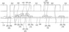
도 23은 본 발명의 제3 실시예에 따른 액정 표시 장치용 박막 트랜지스터 기판의 구조를 도시한 배치도이고, 도 24는 도 23에서 XXIII-XXIII' 선을 따라 잘라 도시한 단면도이다.FIG. 23 is a layout view illustrating a structure of a thin film transistor substrate for a liquid crystal display according to a third exemplary embodiment of the present invention, and FIG. 24 is a cross-sectional view taken along the line XXIII-XXIII 'of FIG. 23.
대부분의 구조는 도 1 및 도 2와 대개 동일하다.Most of the structure is usually the same as in FIGS. 1 and 2.
하지만, 보호막(180) 하부의 화소 영역에는 드레인 전극(175)과 유지 축전기용 도전체 패턴(177)을 드러내는 개구부(C1, C2)를 가지는 적, 녹, 청의 컬러 필터(R, G, B)가 세로 방향으로 형성되어 있다. 여기서, 적, 녹, 청의 컬러 필터(R, G, B)의 경계는 데이터선(171) 상부에서 일치하여 도시되어 있지만, 데이터선(171) 상부에서 서로 중첩되어 화소 영역 사이에서 누설되는 빛을 차단하는 기능을 가질 수 있으며, 게이트선 및 데이터선 각각의 끝 부분(125, 179)이 배치되어 있는 패드부에서는 형성되어 있지 않다.However, red, green, and blue color filters R, G, and B having openings C1 and C2 exposing the
청, 녹, 청의 컬러 필터(R, G, B) 상부의 보호막(180)은 게이트 절연막(140)과 함께 게이트선의 끝 부분(125), 데이터선의 끝 부분(179), 드레인 전극(175) 및 유지 축전기용 도전체(177)를 드러내는 접촉 구멍(182, 189, 185, 187)을 가지고 있다. 이때, 드레인 전극(175) 및 유지 축전기용 도전체(177)를 드러내는 접촉 구멍(185, 187)은 컬러 필터(R, G, B)의 개구부(C1, C2) 안쪽에 위치한다.The
이러한 COA 구조의 액정 표시 장치용 박막 트랜지스터 기판의 구조에서도 제1 및 제2 실시예에서와 같이 동일한 효과를 얻을 수 있다.The same effect can be obtained in the structure of the thin film transistor substrate for a liquid crystal display device having the COA structure as in the first and second embodiments.
이와 같이, 본 발명에 따르면 접촉부에서 드레인 전극의 경계면이 드러나도록 할 때 드레인 전극 하부의 절연막을 잔류시킴으로써 배선의 하부에서 언더 컷이 발생하는 것을 방지할 수 있어, 접촉부의 프로파일을 완만하게 형성할 수 있으며, 이를 통하여 접촉부에서 화소 전극이 단선되는 것을 방지할 수 있다. 접촉 저항이 낮은 도전막을 드러내어 접촉부를 형성함으로써 접촉부의 접촉 저항을 최소화할 수 있어 접촉부의 신뢰성을 확보할 수 있다. 또한, 저저항의 알루미늄 또는 알루미늄 합금을 포함하는 도전막을 포함하는 배선을 형성함으로써 대화면 고정세의 제품의 특성을 향상시킬 수 있다. 또한, 제조 공정을 단순화하여 액정 표시 장치용 박막 트랜지스터 표시판을 제조함으로 제조 공정을 단순화하고 제조 비용을 줄일 수 있다.As described above, according to the present invention, when the interface of the drain electrode is exposed at the contact portion, the insulating film under the drain electrode remains to prevent the undercut from occurring at the bottom of the wiring, so that the profile of the contact portion can be smoothly formed. This prevents disconnection of the pixel electrode at the contact portion. By forming a contact portion by exposing a conductive film having a low contact resistance, the contact resistance of the contact portion can be minimized, thereby ensuring the reliability of the contact portion. In addition, by forming a wiring including a conductive film containing low resistance aluminum or an aluminum alloy, the characteristics of a large screen high definition product can be improved. In addition, the manufacturing process may be simplified to manufacture the thin film transistor array panel for the liquid crystal display, thereby simplifying the manufacturing process and reducing the manufacturing cost.
Claims (15)
Translated fromKoreanPriority Applications (8)
| Application Number | Priority Date | Filing Date | Title |
|---|---|---|---|
| KR1020030003299AKR100925458B1 (en) | 2003-01-17 | 2003-01-17 | Thin film transistor array panel and manufacturing method thereof |
| TW093101177ATWI393970B (en) | 2003-01-17 | 2004-01-16 | Thin film transistor array panel and manufacturing method thereof |
| US10/759,389US7265799B2 (en) | 2003-01-17 | 2004-01-16 | Thin film transistor array panel and manufacturing method thereof |
| CNB2004100009939ACN100399169C (en) | 2003-01-17 | 2004-01-17 | Thin film transistor array panel and manufacturing method thereof |
| JP2004010250AJP2004226975A (en) | 2003-01-17 | 2004-01-19 | Thin film transistor panel and method of manufacturing the same |
| US11/690,563US7742118B2 (en) | 2003-01-17 | 2007-03-23 | Thin film transistor array panel and manufacturing method thereof |
| US11/741,470US7403240B2 (en) | 2003-01-17 | 2007-04-27 | Thin film transistor array panel and manufacturing method thereof |
| US12/141,623US8068188B2 (en) | 2003-01-17 | 2008-06-18 | Thin film transistor array panel and manufacturing method thereof |
Applications Claiming Priority (1)
| Application Number | Priority Date | Filing Date | Title |
|---|---|---|---|
| KR1020030003299AKR100925458B1 (en) | 2003-01-17 | 2003-01-17 | Thin film transistor array panel and manufacturing method thereof |
Publications (2)
| Publication Number | Publication Date |
|---|---|
| KR20040066282A KR20040066282A (en) | 2004-07-27 |
| KR100925458B1true KR100925458B1 (en) | 2009-11-06 |
Family
ID=32906502
Family Applications (1)
| Application Number | Title | Priority Date | Filing Date |
|---|---|---|---|
| KR1020030003299AExpired - LifetimeKR100925458B1 (en) | 2003-01-17 | 2003-01-17 | Thin film transistor array panel and manufacturing method thereof |
Country Status (5)
| Country | Link |
|---|---|
| US (4) | US7265799B2 (en) |
| JP (1) | JP2004226975A (en) |
| KR (1) | KR100925458B1 (en) |
| CN (1) | CN100399169C (en) |
| TW (1) | TWI393970B (en) |
Cited By (1)
| Publication number | Priority date | Publication date | Assignee | Title |
|---|---|---|---|---|
| KR20150066058A (en)* | 2013-12-06 | 2015-06-16 | 삼성디스플레이 주식회사 | Display device and method of manufacturing display device using the same |
Families Citing this family (29)
| Publication number | Priority date | Publication date | Assignee | Title |
|---|---|---|---|---|
| KR20060016920A (en)* | 2004-08-19 | 2006-02-23 | 삼성전자주식회사 | Thin film transistor array panel and manufacturing method thereof |
| KR101058122B1 (en)* | 2004-09-08 | 2011-08-24 | 삼성전자주식회사 | Array substrate, its manufacturing method and liquid crystal panel provided with the same |
| CN101044627B (en)* | 2004-09-15 | 2012-02-08 | 株式会社半导体能源研究所 | Semiconductor device |
| KR101112544B1 (en) | 2004-12-03 | 2012-03-13 | 삼성전자주식회사 | Thin film transistor array panel and method for manufacturing the same |
| KR20060069081A (en) | 2004-12-17 | 2006-06-21 | 삼성전자주식회사 | Thin film transistor array panel and manufacturing method thereof |
| KR101090258B1 (en)* | 2005-01-03 | 2011-12-06 | 삼성전자주식회사 | Method of manufacturing thin film transistor array panel using plastic substrate |
| JP4780986B2 (en)* | 2005-03-23 | 2011-09-28 | シャープ株式会社 | Circuit board manufacturing method |
| KR101219041B1 (en)* | 2005-07-07 | 2013-01-07 | 삼성디스플레이 주식회사 | Thin film transistor array panel and manufacturing method thereof |
| KR101217157B1 (en)* | 2005-10-20 | 2012-12-31 | 엘지디스플레이 주식회사 | Array substrate for Liquid Crystal Display Device and method of fabricating the same |
| KR101174429B1 (en)* | 2006-01-24 | 2012-08-23 | 삼성전자주식회사 | Thin film transistor and method for manufacturing the same and liquid crystal display having the same |
| CN100552898C (en)* | 2006-01-24 | 2009-10-21 | 友达光电股份有限公司 | Thin film transistor and method of manufacturing the same |
| KR101251995B1 (en) | 2006-01-27 | 2013-04-08 | 삼성디스플레이 주식회사 | Thin film transistor array panel and method for manufacturing the same |
| KR101275802B1 (en)* | 2006-06-22 | 2013-06-18 | 삼성디스플레이 주식회사 | Method for fabrication plate for liquid crystal display panel using the mulitlayer dry film resist |
| JP5042662B2 (en)* | 2007-02-21 | 2012-10-03 | 三菱電機株式会社 | Liquid crystal display device and manufacturing method thereof |
| KR101394434B1 (en)* | 2007-06-29 | 2014-05-15 | 삼성디스플레이 주식회사 | Display apparatus and driving method thereof |
| CN102034749B (en)* | 2009-09-25 | 2013-09-04 | 北京京东方光电科技有限公司 | Array substrate and manufacturing method thereof |
| US20120236225A1 (en)* | 2009-12-01 | 2012-09-20 | Sharp Kabushiki Kaisha | Display device substrate, manufacturing method of display device substrate, display device, and manufacturing method of display device |
| KR20120036186A (en)* | 2010-10-07 | 2012-04-17 | 삼성전자주식회사 | Wiring, fabrication method of the wiring, display apparatus having the wiring, and fabrication method of the display apparatus |
| JP5667868B2 (en)* | 2010-12-24 | 2015-02-12 | 株式会社半導体エネルギー研究所 | Method for manufacturing semiconductor device |
| JP2012186297A (en)* | 2011-03-04 | 2012-09-27 | Fujitsu Ltd | Thermoelectric conversion module and manufacturing method therefor |
| TWI451179B (en)* | 2011-11-17 | 2014-09-01 | Au Optronics Corp | Pixel structure and its manufacturing method |
| KR20140020565A (en)* | 2012-08-09 | 2014-02-19 | 삼성디스플레이 주식회사 | Organic light emitting display apparatus and method of manufacturing organic light emitting display apparatus |
| CN102981340B (en) | 2012-12-11 | 2015-11-25 | 京东方科技集团股份有限公司 | A kind of array base palte of liquid crystal display and manufacture method |
| KR101994974B1 (en)* | 2013-01-10 | 2019-07-02 | 삼성디스플레이 주식회사 | Thin film trannsistor array panel and manufacturing method thereof |
| CN103730413B (en)* | 2013-12-31 | 2016-08-17 | 合肥京东方光电科技有限公司 | The preparation method of a kind of array base palte and array base palte, display device |
| WO2016084700A1 (en)* | 2014-11-28 | 2016-06-02 | シャープ株式会社 | Semiconductor device and method for manufacturing same |
| KR102717808B1 (en) | 2016-11-30 | 2024-10-15 | 엘지디스플레이 주식회사 | Display device having a plurality of insulating layer disposed between two electrodes |
| KR102623558B1 (en)* | 2018-11-14 | 2024-01-10 | 삼성디스플레이 주식회사 | Display device |
| KR20190088929A (en)* | 2019-07-09 | 2019-07-29 | 엘지전자 주식회사 | Display device using micro led and manufacturing method thereof |
Citations (3)
| Publication number | Priority date | Publication date | Assignee | Title |
|---|---|---|---|---|
| KR20000029304A (en)* | 1998-10-26 | 2000-05-25 | 마찌다 가쯔히꼬 | Liquid crystal display device and method for manufacturing the same |
| KR20010082831A (en)* | 2000-02-21 | 2001-08-31 | 구본준, 론 위라하디락사 | Method of Fabricating Liquid Crystal Display Device |
| KR20020010212A (en)* | 2000-07-27 | 2002-02-04 | 윤종용 | Thin film transistor array panel and method manufacturing the same |
Family Cites Families (19)
| Publication number | Priority date | Publication date | Assignee | Title |
|---|---|---|---|---|
| TW329500B (en)* | 1995-11-14 | 1998-04-11 | Handotai Energy Kenkyusho Kk | Electro-optical device |
| JPH09244065A (en)* | 1996-03-08 | 1997-09-19 | Toshiba Electron Eng Corp | Active matrix type liquid crystal display |
| JP4363684B2 (en)* | 1998-09-02 | 2009-11-11 | エルジー ディスプレイ カンパニー リミテッド | Thin film transistor substrate and liquid crystal display device using the same |
| US6255130B1 (en)* | 1998-11-19 | 2001-07-03 | Samsung Electronics Co., Ltd. | Thin film transistor array panel and a method for manufacturing the same |
| JP3267271B2 (en)* | 1998-12-10 | 2002-03-18 | 日本電気株式会社 | Liquid crystal display device and method of manufacturing the same |
| US6380559B1 (en)* | 1999-06-03 | 2002-04-30 | Samsung Electronics Co., Ltd. | Thin film transistor array substrate for a liquid crystal display |
| KR100310946B1 (en) | 1999-08-07 | 2001-10-18 | 구본준, 론 위라하디락사 | Liguid crystal Display Device and the same method |
| CN1195243C (en)* | 1999-09-30 | 2005-03-30 | 三星电子株式会社 | Film transistor array panel for liquid crystal display and its producing method |
| JP2001214638A (en)* | 2000-02-03 | 2001-08-10 | Takeshi Inoue | Column supporting device |
| JP2002196700A (en) | 2000-12-22 | 2002-07-12 | Matsushita Electric Ind Co Ltd | Semiconductor device, manufacturing method thereof, liquid crystal display device using the same, and electroluminescence display device |
| KR100392850B1 (en)* | 2000-12-29 | 2003-07-28 | 엘지.필립스 엘시디 주식회사 | Liquid Crystal Display Device and Fabricating Method Thereof |
| KR20020083249A (en)* | 2001-04-26 | 2002-11-02 | 삼성전자 주식회사 | A contact structure of a wires and method manufacturing the same, and thin film transistor substrate including the contact structure and method manufacturing the same |
| KR100731037B1 (en) | 2001-05-07 | 2007-06-22 | 엘지.필립스 엘시디 주식회사 | LCD and its manufacturing method |
| US6888586B2 (en)* | 2001-06-05 | 2005-05-03 | Lg. Philips Lcd Co., Ltd. | Array substrate for liquid crystal display and method for fabricating the same |
| KR100796795B1 (en)* | 2001-10-22 | 2008-01-22 | 삼성전자주식회사 | A contact portion of a semiconductor device, a method of manufacturing the same, and a thin film transistor array substrate for a display device including the same, and a method of manufacturing the same |
| KR100391157B1 (en)* | 2001-10-25 | 2003-07-16 | 엘지.필립스 엘시디 주식회사 | array panel of liquid crystal display and manufacturing method thereof |
| US7126650B2 (en) | 2002-03-29 | 2006-10-24 | Matsushita Electric Industrial Co., Ltd. | Illumination unit and liquid crystal display apparatus comprising same |
| US7023016B2 (en)* | 2003-07-02 | 2006-04-04 | Samsung Electronics Co., Ltd. | Thin film transistor array panel and manufacturing method thereof |
| US7760317B2 (en)* | 2003-10-14 | 2010-07-20 | Lg Display Co., Ltd. | Thin film transistor array substrate and fabricating method thereof, liquid crystal display using the same and fabricating method thereof, and method of inspecting liquid crystal display |
- 2003
- 2003-01-17KRKR1020030003299Apatent/KR100925458B1/ennot_activeExpired - Lifetime
- 2004
- 2004-01-16USUS10/759,389patent/US7265799B2/ennot_activeExpired - Fee Related
- 2004-01-16TWTW093101177Apatent/TWI393970B/ennot_activeIP Right Cessation
- 2004-01-17CNCNB2004100009939Apatent/CN100399169C/ennot_activeExpired - Lifetime
- 2004-01-19JPJP2004010250Apatent/JP2004226975A/enactivePending
- 2007
- 2007-03-23USUS11/690,563patent/US7742118B2/enactiveActive
- 2007-04-27USUS11/741,470patent/US7403240B2/ennot_activeExpired - Lifetime
- 2008
- 2008-06-18USUS12/141,623patent/US8068188B2/ennot_activeExpired - Lifetime
Patent Citations (3)
| Publication number | Priority date | Publication date | Assignee | Title |
|---|---|---|---|---|
| KR20000029304A (en)* | 1998-10-26 | 2000-05-25 | 마찌다 가쯔히꼬 | Liquid crystal display device and method for manufacturing the same |
| KR20010082831A (en)* | 2000-02-21 | 2001-08-31 | 구본준, 론 위라하디락사 | Method of Fabricating Liquid Crystal Display Device |
| KR20020010212A (en)* | 2000-07-27 | 2002-02-04 | 윤종용 | Thin film transistor array panel and method manufacturing the same |
Cited By (2)
| Publication number | Priority date | Publication date | Assignee | Title |
|---|---|---|---|---|
| KR20150066058A (en)* | 2013-12-06 | 2015-06-16 | 삼성디스플레이 주식회사 | Display device and method of manufacturing display device using the same |
| KR102233457B1 (en)* | 2013-12-06 | 2021-03-30 | 삼성디스플레이 주식회사 | Display device and method of manufacturing display device using the same |
Also Published As
| Publication number | Publication date |
|---|---|
| JP2004226975A (en) | 2004-08-12 |
| US20040183955A1 (en) | 2004-09-23 |
| CN100399169C (en) | 2008-07-02 |
| US20070200981A1 (en) | 2007-08-30 |
| US20080252806A1 (en) | 2008-10-16 |
| US7742118B2 (en) | 2010-06-22 |
| US7265799B2 (en) | 2007-09-04 |
| KR20040066282A (en) | 2004-07-27 |
| CN1517771A (en) | 2004-08-04 |
| US8068188B2 (en) | 2011-11-29 |
| US20070190706A1 (en) | 2007-08-16 |
| US7403240B2 (en) | 2008-07-22 |
| TWI393970B (en) | 2013-04-21 |
| TW200500707A (en) | 2005-01-01 |
Similar Documents
| Publication | Publication Date | Title |
|---|---|---|
| KR100925458B1 (en) | Thin film transistor array panel and manufacturing method thereof | |
| KR100796795B1 (en) | A contact portion of a semiconductor device, a method of manufacturing the same, and a thin film transistor array substrate for a display device including the same, and a method of manufacturing the same | |
| KR100870013B1 (en) | Thin film transistor array substrate and manufacturing method thereof | |
| KR100905472B1 (en) | Thin film transistor array substrate and liquid crystal display including the same | |
| KR100905470B1 (en) | Thin film transistor array substrate | |
| KR100333979B1 (en) | Methods for manufacturing thin film transistor panels for liquid crystal display | |
| KR20010060519A (en) | Thin film transistor panels for liquid crystal display and methods for manufacturing the same | |
| KR20030055125A (en) | Thin film transistor array panel and method for manufacturing the panel | |
| KR100910563B1 (en) | Thin film transistor array panel | |
| KR100750919B1 (en) | Thin film transistor substrate for liquid crystal display device and manufacturing method thereof | |
| KR100330097B1 (en) | Thin film transistor substrate for liquid crystal display and manufacturing method thereof | |
| KR20010096804A (en) | A contact structure of a wires and method manufacturing the same, and thin film transistor substrate including the contact structure and method manufacturing the same | |
| KR20030094606A (en) | A contact portion of a wires, and thin film transistor substrate including the contact portion | |
| KR100796746B1 (en) | Manufacturing method of thin film transistor substrate for liquid crystal display device | |
| KR100870009B1 (en) | Contact portion of wiring, manufacturing method thereof, and thin film transistor array substrate including same and manufacturing method thereof | |
| KR100910566B1 (en) | Method of manufacturing thin film transistor array panel and mask therefor | |
| KR100920352B1 (en) | Thin film transistor array panel | |
| KR100729776B1 (en) | Thin film transistor substrate for liquid crystal display device and manufacturing method thereof | |
| KR20010017529A (en) | Thin film transistor substrate for liquid crystal display and manufacturing method thereof | |
| KR100915237B1 (en) | Method for manufacturing thin film transistor array panel and mask for manufacturing the panel | |
| KR100853207B1 (en) | Thin film transistor substrate for liquid crystal display device and manufacturing method thereof | |
| KR100864486B1 (en) | Thin film transistor substrate for liquid crystal display device and manufacturing method thereof | |
| KR100560971B1 (en) | Manufacturing method of thin film transistor substrate for liquid crystal display device | |
| KR100777699B1 (en) | Thin film transistor substrate for liquid crystal display device and manufacturing method thereof | |
| KR100720096B1 (en) | Thin film transistor substrate for liquid crystal display device and manufacturing method thereof |
Legal Events
| Date | Code | Title | Description |
|---|---|---|---|
| PA0109 | Patent application | Patent event code:PA01091R01D Comment text:Patent Application Patent event date:20030117 | |
| PG1501 | Laying open of application | ||
| A201 | Request for examination | ||
| PA0201 | Request for examination | Patent event code:PA02012R01D Patent event date:20080108 Comment text:Request for Examination of Application Patent event code:PA02011R01I Patent event date:20030117 Comment text:Patent Application | |
| E902 | Notification of reason for refusal | ||
| PE0902 | Notice of grounds for rejection | Comment text:Notification of reason for refusal Patent event date:20090112 Patent event code:PE09021S01D | |
| E902 | Notification of reason for refusal | ||
| PE0902 | Notice of grounds for rejection | Comment text:Notification of reason for refusal Patent event date:20090714 Patent event code:PE09021S01D | |
| E701 | Decision to grant or registration of patent right | ||
| PE0701 | Decision of registration | Patent event code:PE07011S01D Comment text:Decision to Grant Registration Patent event date:20090922 | |
| GRNT | Written decision to grant | ||
| PR0701 | Registration of establishment | Comment text:Registration of Establishment Patent event date:20091030 Patent event code:PR07011E01D | |
| PR1002 | Payment of registration fee | Payment date:20091102 End annual number:3 Start annual number:1 | |
| PG1601 | Publication of registration | ||
| FPAY | Annual fee payment | Payment date:20121015 Year of fee payment:4 | |
| PR1001 | Payment of annual fee | Payment date:20121015 Start annual number:4 End annual number:4 | |
| FPAY | Annual fee payment | Payment date:20130930 Year of fee payment:5 | |
| PR1001 | Payment of annual fee | Payment date:20130930 Start annual number:5 End annual number:5 | |
| FPAY | Annual fee payment | Payment date:20141001 Year of fee payment:6 | |
| PR1001 | Payment of annual fee | Payment date:20141001 Start annual number:6 End annual number:6 | |
| FPAY | Annual fee payment | Payment date:20150930 Year of fee payment:7 | |
| PR1001 | Payment of annual fee | Payment date:20150930 Start annual number:7 End annual number:7 | |
| FPAY | Annual fee payment | Payment date:20170928 Year of fee payment:9 | |
| PR1001 | Payment of annual fee | Payment date:20170928 Start annual number:9 End annual number:9 | |
| FPAY | Annual fee payment | Payment date:20181001 Year of fee payment:10 | |
| PR1001 | Payment of annual fee | Payment date:20181001 Start annual number:10 End annual number:10 | |
| PR1001 | Payment of annual fee | Payment date:20201005 Start annual number:12 End annual number:12 | |
| PR1001 | Payment of annual fee | Payment date:20210927 Start annual number:13 End annual number:13 | |
| PC1801 | Expiration of term | Termination date:20230717 Termination category:Expiration of duration |