KR100924046B1 - Image sensor and its manufacturing method - Google Patents
Image sensor and its manufacturing methodDownload PDFInfo
- Publication number
- KR100924046B1 KR100924046B1KR1020070139366AKR20070139366AKR100924046B1KR 100924046 B1KR100924046 B1KR 100924046B1KR 1020070139366 AKR1020070139366 AKR 1020070139366AKR 20070139366 AKR20070139366 AKR 20070139366AKR 100924046 B1KR100924046 B1KR 100924046B1
- Authority
- KR
- South Korea
- Prior art keywords
- planarization layer
- micro lens
- color filter
- interlayer insulating
- disposed
- Prior art date
- Legal status (The legal status is an assumption and is not a legal conclusion. Google has not performed a legal analysis and makes no representation as to the accuracy of the status listed.)
- Expired - Fee Related
Links
Images


Classifications
- H—ELECTRICITY
- H10—SEMICONDUCTOR DEVICES; ELECTRIC SOLID-STATE DEVICES NOT OTHERWISE PROVIDED FOR
- H10F—INORGANIC SEMICONDUCTOR DEVICES SENSITIVE TO INFRARED RADIATION, LIGHT, ELECTROMAGNETIC RADIATION OF SHORTER WAVELENGTH OR CORPUSCULAR RADIATION
- H10F39/00—Integrated devices, or assemblies of multiple devices, comprising at least one element covered by group H10F30/00, e.g. radiation detectors comprising photodiode arrays
- H10F39/80—Constructional details of image sensors
- H10F39/806—Optical elements or arrangements associated with the image sensors
- H10F39/8063—Microlenses
- H—ELECTRICITY
- H10—SEMICONDUCTOR DEVICES; ELECTRIC SOLID-STATE DEVICES NOT OTHERWISE PROVIDED FOR
- H10F—INORGANIC SEMICONDUCTOR DEVICES SENSITIVE TO INFRARED RADIATION, LIGHT, ELECTROMAGNETIC RADIATION OF SHORTER WAVELENGTH OR CORPUSCULAR RADIATION
- H10F39/00—Integrated devices, or assemblies of multiple devices, comprising at least one element covered by group H10F30/00, e.g. radiation detectors comprising photodiode arrays
- H10F39/011—Manufacture or treatment of image sensors covered by group H10F39/12
- H10F39/024—Manufacture or treatment of image sensors covered by group H10F39/12 of coatings or optical elements
- H—ELECTRICITY
- H10—SEMICONDUCTOR DEVICES; ELECTRIC SOLID-STATE DEVICES NOT OTHERWISE PROVIDED FOR
- H10F—INORGANIC SEMICONDUCTOR DEVICES SENSITIVE TO INFRARED RADIATION, LIGHT, ELECTROMAGNETIC RADIATION OF SHORTER WAVELENGTH OR CORPUSCULAR RADIATION
- H10F39/00—Integrated devices, or assemblies of multiple devices, comprising at least one element covered by group H10F30/00, e.g. radiation detectors comprising photodiode arrays
- H10F39/80—Constructional details of image sensors
- H10F39/805—Coatings
Landscapes
- Solid State Image Pick-Up Elements (AREA)
Abstract
Translated fromKoreanDescription
Translated fromKorean실시예에서는 이미지 센서 및 그 제조방법이 개시된다.In an embodiment, an image sensor and a method of manufacturing the same are disclosed.
이미지 센서는 광학적 영상(Optical Image)을 전기 신호로 변환시키는 반도체 소자로서, 크게 전하결합소자(charge coupled device:CCD) 이미지 센서와 씨모스(Complementary Metal Oxide Silicon:CMOS) 이미지 센서(CIS)로 구분된다.An image sensor is a semiconductor device that converts an optical image into an electrical signal, and is classified into a charge coupled device (CCD) image sensor and a complementary metal oxide silicon (CMOS) image sensor (CIS). do.
씨모스 이미지센서는 단위 화소 내에 포토 다이오드와 모스 트랜지스터를 형성시키는 스위칭 방식으로 각 단위 화소의 전기적 신호를 순차적으로 검출하여 영상을 구현한다.The CMOS image sensor implements an image by sequentially detecting an electrical signal of each unit pixel in a switching method of forming a photodiode and a MOS transistor in the unit pixel.
씨모스 이미지 센서의 광감도를 향상시키기 위하여 컬러필터 상에 마이크로렌즈를 형성하는 방법이 있다. 마이크로렌즈는 감광성 유기물 물질을 노광(expose), 현상(development) 및 리플로우(reflow)의 순서로 진행하여 반구형의 모양을 최종 형성시킨다. 그러면 단위화소 상에 마이크로 렌즈가 형성되어 빛을 포토다이오드로 집광시킬 수 있다. 이러한 마이크로 렌즈는 단위화소 별로 각각 형성되고 상기 마이크로 렌즈의 크기 및 개수에 따라 입사광의 양이 변화될 수 있다.There is a method of forming a microlens on a color filter in order to improve light sensitivity of the CMOS image sensor. The microlens advances the photosensitive organic material in the order of exposure, development and reflow to finally form a hemispherical shape. As a result, a microlens may be formed on the unit pixel to condense light with the photodiode. The microlenses are formed for each unit pixel, and the amount of incident light may vary according to the size and number of the microlenses.
실시예에서는 포토다이오드의 광감지율을 향상시킬 수 있는 이미지 센서 및 그 제조방법을 제공한다.The embodiment provides an image sensor and a method of manufacturing the same that can improve a light sensing ratio of a photodiode.
실시예에 따른 이미지 센서는, 픽셀 영역 및 로직 영역을 포함하는 반도체 기판; 상기 반도체 기판 상에 배치된 금속배선을 포함하는 층간 절연막; 상기 픽셀 영역에 대응하는 상기 층간 절연막 상에 배치된 제1 컬러필터; 상기 로직 영역에 대응하는 상기 층간 절연막 상에 배치된 제2 컬러필터; 상기 제1 및 제2 컬러필터 상에 배치된 제1 평탄화층; 상기 제1 평탄화층 상에 배치되고 상기 제2 컬러필터에 대응하는 영역에 오목형의 제2 마이크로 렌즈가 형성된 제2 평탄화층; 및 상기 제2 평탄화층 상에 배치되고 상기 제1 컬러필터에 대응하는 영역에 볼록형의 제1 마이크로 렌즈가를 포함한다.An image sensor according to an embodiment includes a semiconductor substrate including a pixel region and a logic region; An interlayer insulating film including metal wires disposed on the semiconductor substrate; A first color filter disposed on the interlayer insulating layer corresponding to the pixel area; A second color filter disposed on the interlayer insulating layer corresponding to the logic region; First planarization layers disposed on the first and second color filters; A second planarization layer disposed on the first planarization layer and having a concave second micro lens formed in a region corresponding to the second color filter; And a convex first micro lens disposed on the second planarization layer and corresponding to the first color filter.
실시예에 따른 이미지 센서는, 반도체 기판상에 픽셀 영역 및 로직 영역을 형성하는 단계; 상기 반도체 기판 상에 금속배선을 포함하는 층간 절연막을 형성하는 단계; 상기 픽셀 영역에 대응하는 상기 층간 절연막 상에 제1 컬러필터를 형성하는 단계; 상기 로직 영역에 대응하는 상기 층간 절연막 상에 제2 컬러필터를 형성하는 단계; 상기 제1 및 제2 컬러필터를 포함하는 층간 절연막 상에 제1 평탄화층을 형성하는 단계; 상기 제1 평탄화층 상에 제2 평탄화층을 형성하는 단계; 상기 제1 컬러필터에 대응하도록 상기 제2 평탄화층 상에 볼록형의 제1 마이크로 렌즈를 형성하는 단계; 및 상기 제2 컬러필터에 대응하도록 상기 제2 평탄화층에 오목형의 제2 마이크로 렌즈를 형성하는 단계를 포함한다.An image sensor according to an embodiment includes forming a pixel region and a logic region on a semiconductor substrate; Forming an interlayer insulating film including metal wiring on the semiconductor substrate; Forming a first color filter on the interlayer insulating layer corresponding to the pixel region; Forming a second color filter on the interlayer insulating layer corresponding to the logic region; Forming a first planarization layer on the interlayer insulating film including the first and second color filters; Forming a second planarization layer on the first planarization layer; Forming a convex first micro lens on the second planarization layer to correspond to the first color filter; And forming a concave second micro lens in the second planarization layer to correspond to the second color filter.
실시예에 따른 이미지 센서 및 그 제조방법에 의하면, 볼록형 마이크로 렌즈 주변에 오목형 마이크로 렌즈가 형성되어 포토다이오드의 집광율을 향상시킬 수 있다.According to the image sensor and the manufacturing method thereof according to the embodiment, a concave micro lens is formed around the convex micro lens to improve the light condensation rate of the photodiode.
실시예에 따른 이미지 센서 및 그 제조방법을 첨부된 도면을 참조하여 상세히 설명한다.An image sensor and a method of manufacturing the same according to an embodiment will be described in detail with reference to the accompanying drawings.
실시예의 설명에 있어서, 각 층의 "상/위(on/over)"에 형성되는 것으로 기재되는 경우에 있어, 상/위(on/over)는 직접(directly)와 또는 다른 층을 개재하여(indirectly) 형성되는 것을 모두 포함한다.In the description of the embodiments, where described as being formed "on / over" of each layer, the on / over may be directly or through another layer ( indirectly) includes everything formed.
도면에서 각층의 두께나 크기는 설명의 편의 및 명확성을 위하여 과장되거나 생략되거나 또는 개략적으로 도시되었다. 또한 각 구성요소의 크기는 실제크기를 전적으로 반영하는 것은 아니다.In the drawings, the thickness or size of each layer is exaggerated, omitted, or schematically illustrated for convenience and clarity of description. In addition, the size of each component does not necessarily reflect the actual size.
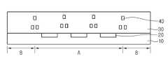
도 6은 실시예에 따른 이미지 센서를 도시한 단면도이다.6 is a cross-sectional view illustrating an image sensor according to an embodiment.
실시예에 따른 이미지 센서는, 픽셀 영역(A) 및 로직 영역(B)을 포함하는 반도체 기판(10)과, 상기 반도체 기판(10) 상에 배치된 금속배선(40)을 포함하는 층간 절연막(30)과, 상기 픽셀 영역(A)에 대응하는 상기 층간 절연막(30) 상에 배치된 제1 컬러필터(50)와, 상기 로직 영역(B)에 대응하는 상기 층간 절연막(30) 상에 배치된 제2 컬러필터(60); 상기 제1 및 제2 컬러필터(50,60) 상에 배치된 제1 평탄화층(70); 상기 제1 평탄화층(70) 상에 배치되고 상기 제2 컬러필터(60)에 대응하는 영역에 오목형의 제2 마이크로 렌즈(100)가 형성된 제2 평탄화층(80); 및 상기 제2 평탄화층(80) 상에 배치되고 상기 제1 컬러필터(50)에 대응하는 영역에 볼록형의 제1 마이크로 렌즈(90)가 배치된 것을 포함한다.An image sensor according to an embodiment may include an interlayer insulating layer including a
상기 제1 평탄화층(70)은 상기 제1 및 제2 컬러필터(50,60)의 단차를 보완하기 위한 것으로 포토레지스트막으로 형성될 수 있다.The
상기 제2 평탄화층(80)은 SOG(Spin On Glass) 계열의 물질로 형성될 수 있다. 예를 들어, 상기 제2 평탄화층(80)은 Organic SOG, Inorganic HSQ(Hydrosilseqeoxane), MSQ(Methylsilseqeoxane)와 같은 SOG 물질일 수 있다.The
상기 제2 평탄화층(80)에 형성된 오목형의 제2 마이크로 렌즈(100)는 반도체 기판(10)의 테두리 영역에 배치될 수 있다The concave second
실시예에 따른 이미지 센서는, 볼록형의 마이크로 렌즈 주변에 오목형의 마이크로 렌즈가 형성되어 포토다이오드의 필팩터를 향상시킬 수 있다.In the image sensor according to the embodiment, a concave micro lens is formed around the convex micro lens to improve the fill factor of the photodiode.
도 1 내지 도 7을 참조하여 실시예에 따른 이미지 센서의 제조방법을 설명한다.A method of manufacturing an image sensor according to an embodiment will be described with reference to FIGS. 1 to 7.
도 1을 참조하여, 반도체 기판(10) 상에 픽셀 영역(A) 및 로직 영역(B)이 형성된다.Referring to FIG. 1, a pixel region A and a logic region B are formed on a
상기 반도체 기판(10)에 액티브 영역과 필드 영역을 정의하는 복수개의 소자분리막(미도시)이 형성된다. 또한, 상기 액티브 영역 상에는 픽셀 영역(A) 및 로직 영역(B)이 형성된다.A plurality of device isolation layers (not shown) defining an active region and a field region are formed in the
상기 픽셀 영역(A)에는 빛을 수광하여 광전하를 생성하는 포토다이오드(20) 및 상기 포토다이오드(20)에 연결되어 수광된 광전하를 전기신호를 변환하기 위하여 트랜지스터(미도시)가 단위화소 별로 형성될 수 있다. 예를 들어, 상기 트랜지스터 회로는 3Tr, 4Tr 및 5Tr 중 어느 하나 일 수 있다.In the pixel region A, a
상기 로직 영역(B)에는 상기 픽셀 영역(A)의 각 단위화소의 전기적 신호를 순차적으로 검출하여 영상을 구현하기 위한 트랜지스터 회로(미도시)가 형성될 수 있다.In the logic region B, a transistor circuit (not shown) may be formed to sequentially detect an electrical signal of each unit pixel of the pixel region A to implement an image.
상기 포토다이오드(20)를 포함하는 관련소자들이 형성된 이후에 상기 반도체 기판(10) 상에 금속배선(40)을 포함하는 층간 절연막(30)이 형성된다.After the related devices including the
상기 금속배선(40)은 전원라인 및 신호라인과 픽셀 영역(A) 및 로직 영역(B)의 트랜지스터를 접속시키기 위한 것으로 복수의 층으로 형성될 수 있다. 즉, 층간 절연막(30)은 복수의 층으로 형성될 수 있으며, 상기 층간 절연막(30)을 관통하는 상기 금속배선(40)도 복수개로 형성되어 전기적으로 접촉된 상태로 형성될 수 있다. 상기 금속배선(40)은 포토다이오드(20)로 입사되는 빛을 가리지 않도록 의도적으로 레이아웃되어 형성된다. 예를 들어, 상기 층간 절연막(30)은 산화막 물질로 형성될 수 있으며, 상기 금속배선(40)은 금속, 합금 또는 실리사이드를 포함한 다양한 전도성 물질, 즉 알루미늄, 구리, 코발트 또는 텅스텐 등으로 형성될 수 있다.The
상기 층간 절연막(30)은 패시베이션층(미도시)을 포함할 수 있다. 상기 패시 베이션층은 습기나 스크래치 등으로부터 소자를 보호하기 위한 것으로 절연막으로 형성될 수 있다. 한편, 상기 패시베이션층의 형성을 생략할 수도 있다.The
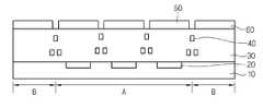
도 2를 참조하여, 상기 층간 절연막(30) 상에 제1 및 제2 컬러필터(50,60)가 형성된다. 상기 제1 컬러필터(50)는 상기 픽셀 영역(A)에 대응하는 상기 층간 절연막(30) 상에 단위화소 별로 형성된다. 상기 제2 컬러필터(60)는 상기 로직 영역(B)에 대응하는 층간 절연막(30) 상에 형성된다. 즉, 상기 제1 컬러필터(50)는 단위픽셀 별로 형성된 포토다이오드(20) 상에 형성되고, 상기 제2 컬러필터(60)는 상기 로직 영역(B)에 배치되어 상기 제1 컬러필터(50)를 둘러싼 구조로 형성될 수 있다.Referring to FIG. 2, first and
상기 제1 및 제2 컬러필터(50,60)는 감광물질 및 안료 또는 감광물질 및 염료를 포함하는 컬러필터층(미도시)을 스핀 코팅 공정등을 통해 상기 층간 절연막(30) 상에 형성한다. 이어서, 상기 컬러필터층을 패턴 마스크에 의하여 노광한 후 현상하면 상기 층간 절연막(30) 상에 제1 및 제2 컬러필터(50,60)가 형성된다.The first and
상기 제1 컬러필터(50)은 각각의 단위화소 마다 하나의 컬러필터가 형성되어 입사하는 빛으로부터 색을 분리해 낸다. 예를 들어, 상기 제1 컬러필터(50)들은 레드(Red), 그린(Green), 블루(Blue)으로 형성되며, 인접한 컬러필터들은 서로 약간씩 오버랩되어 단차가 형성된다.In the
또한, 상기 제2 컬러필터(60)는 상기 제1 컬러필터(50) 중 어느 하나가 형성될 때 동시에 형성될 수 있다. 상기 제2 컬러필터(60)는 레드(Red),그린(Green), 블루(Blue) 중 어느 하나일 수 있다.In addition, the
도 3을 참조하여, 상기 제1 및 제2 컬러필터(50,60) 상에 제1 평탄화층(70) 이 형성된다. 상기 제1 평탄화층(70)은 상기 제1 및 제2 컬러필터(50,60)의 단차를 보완하기 위한 것으로 상기 제1 및 제2 컬러필터(50,60)를 포함하는 층간 절연막(30) 상에 형성된다. 예를 들어, 상기 제1 평탄화층(70)은 산화막 및 유기물막으로 형성될 수 있다.Referring to FIG. 3, a
상기 제1 평탄화층(70) 상에 제2 평탄화층(80)이 형성된다. 상기 제2 평탄화층(80)은 상기 제2 컬러필터(60)에 대응하는 위치에 마이크로 렌즈를 형성하기 위한 것이다. 상기 제2 평탄화층(80)은 SOG(Spin On Glass) 물질을 스핀 코팅(spin coating)하여 형성될 수 있다. 예를 들어, 상기 제2 평탄화층(80)은 Organic SOG, Inorganic HSQ(Hydrosilseqeoxane), MSQ(Methylsilseqeoxane)와 같은 SOG 물질일 수 있다.The
도시되지는 않았지만, 상기 제1 평탄화층(70)을 생략하고 상기 제1 및 제2 컬러필터(50,60)를 포함하는 층간 절연막(30) 상에 제2 평탄화층(80)이 형성될 수도 있다.Although not shown, a
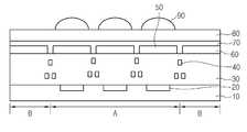
도 4를 참조하여, 상기 제2 평탄화층(80) 상에 반구 형태의 제1 마이크로 렌즈(90)가 형성된다. 상기 제1 마이크로 렌즈(90)는 상기 제1 컬러필터(50)에 대응하는 상기 제2 평탄화층(80) 상에 형성될 수 있다. 즉, 상기 제1 마이크로 렌즈(90)는 상기 픽셀 영역(A)의 포토다이오드(20)에 대응하도록 단위픽셀 별로 형성될 수 있다.Referring to FIG. 4, a hemispherical first
상기 제1 마이크로 렌즈(90)는 마이크로 렌즈용 포토레지스트 또는 저온 산화막으로 형성될 수 있다.The first
예를 들어, 상기 제1 마이크로 렌즈(90)는 상기 제2 평탄화층(80) 상부로 마이크로 렌즈 형성용 포토레지스트를 스핀 공정등을 통해 도포한다. 그리고, 상기 포토레지스트막(미도시)을 선택적으로 노광 및 현상한 후 제1 컬러필터(50) 상부에 포토레지스트 패턴(미도시)을 형성한다. 이후, 리플로우 공정을 실시하여 볼록한 형상을 갖는 돔 형태의 제1 마이크로 렌즈(90)를 형성할 수 있다.For example, the first
또는 상기 제1 마이크로 렌즈(90)는 상기 제2 평탄화층(80) 상부로 저온산화막 및 포토레지스트막을 적층한다. 그리고, 상기 포토레지스트막(미도시)을 선택적으로 노광 및 현상한 후 상기 제1 컬러필터(50) 상부에 희생 마이크로 렌즈(미도시)를 형성한다. 그리고, 상기 희생 마이크로 렌즈를 식각마스크로 사용하여 상기 저온산화막을 식각하면 볼록한 형상을 갖는 돔 형태의 제1 마이크로 렌즈(90)를 형성할 수 있다.Alternatively, the first
따라서, 상기 픽셀 영역(A)에 대응하는 상기 제2 평탄화층(80) 상에 볼록한 형태의 제1 마이크로 렌즈(90)가 형성되고, 상기 로직 영역(B)에 대응하는 상기 제2 평탄화층(80)은 노출된다.Accordingly, a
도 5를 참조하여, 상기 제1 마이크로 렌즈(90)를 포함하는 제2 평탄화층(80) 상에 포토레지스트 패턴(200)이 형성된다. 상기 포토레지스트 패턴(200)은 상기 제2 컬러필터(60)에 대응하는 상기 제2 평탄화층(80)을 부분적을 노출시킬 수 있다.Referring to FIG. 5, a
상기 포토레지스트 패턴(200)은 상기 제1 마이크로 렌즈(90)를 포함하는 제2 평탄화층(80) 상에 포토레지스트막을 스핀공정 등에 의하여 코팅한다. 그리고, 상기 포토레지스트막을 노광 및 현상하여 상기 제2 컬러필터(60)에 대응하는 영역에 오픈홀(210)을 가지는 포토레지스트 패턴(200)을 형성한다.The
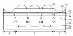
도 6을 참조하여, 상기 제2 컬러필터(60)에 대응하는 상기 제2 평탄화층(80)에 오목한 형태의 제2 마이크로 렌즈(100)가 형성된다. 상기 제2 마이크로 렌즈(100)는 상기 제2 컬러필터(60)에 대응하는 상기 제2 평탄화층(80)에 형성된다. 따라서, 상기 제2 마이크로 렌즈(100)는 상기 반도체 기판(10)의 로직 영역(B)에 대응하도록 형성될 수 있다.Referring to FIG. 6, a second
상기 제2 마이크로 렌즈(100)는 상기 포토레지스트 패턴(200)을 식각 마스크로 사용하여 하부의 제2 평탄화층(80)을 식각하여 형성될 수 있다. 예를 들어, 상기 제2 마이크로 렌즈(100)는 상기 오픈홀(210)에 의하여 노출된 상기 제2 평탄화층(80)에 대한 습식식각 공정에 의하여 형성될 수 있다. 예를 들어, 상기 제2 평탄화층(80)에 대한 습식식각 공정은 BOE(Brffered Oxide Etchant)에 의하여 진행될 수 있다. 상기 BOE는 NH4F:HF;H2O의 혼합 용액일 수 있다.The second
상기 포토레지스트 패턴(200)의 오픈홀(210)에 의하여 노출된 상기 제2 평탄화층(80)이 에천트에 의하여 등방성으로 식각되므로 상기 제2 마이크로 렌즈(100)는 바닥면이 둥근 트랜치 형태로 형성될 수 있다.Since the
상기 제2 마이크로 렌즈(100)는 상기 제2 컬러필터(60)에 대응하는 상기 제2 평탄화층(80)에 오목한 형태로 형성될 수 있다. 또한, 상기 제2 마이크로 렌즈(100)는 상기 제1 마이크로 렌즈(90) 주변에 형성되고 상기 제1 마이크로 렌즈(90)와 반대의 형태로 형성될 수 있다.The second
이후, 상기 포토레지스트 패턴(200)은 애싱공정에 의하여 제거될 수 있다.Thereafter, the
도 7은 도 6의 평면도로서, 상기 제1 및 제2 마이크로 렌즈(100)를 포함하는 이미지 센서의 평면도이다. 도 8은 실시예에 따른 이미지 센서로 빛이 입사되는 상태를 도시한 단면도이다.FIG. 7 is a plan view of FIG. 6, which is a plan view of an image sensor including the first and second
도 7 및 도 8을 참조하여, 상기 픽셀 영역(A)에는 상기 제1 마이크로 렌즈(90)가 형성되어 있다. 또한, 상기 로직 영역(B)에는 제2 마이크로 렌즈(100)가 형성되어 있다.7 and 8, the first
일반적으로, 상기 반도체 기판(10)의 중앙 영역에는 픽셀 영역(A)이 형성되고 상기 픽셀 영역(A)의 주변에 로직 영역(B)이 형성된다. 따라서, 상기 제1 마이크로 렌즈(90)의 주변에 제2 마이크로 렌즈(100)가 형성될 수 있다.In general, a pixel region A is formed in a central region of the
상기와 같이 볼록한 형태의 제1 마이크로 렌즈(90)의 주변에 오목한 형태의 제2 마이크로 렌즈(100)가 형성되므로 포토다이오드(20)의 집광률을 향상시킬 수 있다. 즉, 상기 픽셀 영역(A) 이외의 영역인 로직 영역(B)으로 입사되는 빛이 상기 제2 마이크로 렌즈(100)에 의하여 상기 픽셀 영역(A)으로 모아지므로 포토다이오드(20)의 광특성을 향상시킬 수 있다.Since the concave second
또한, 상기 제2 평탄화층(80)이 SOG막으로 형성되므로 상기 제1 및 제2 컬러필터(50,60)의 토폴로지(Topology)를 평탄화시킬 수 있다. 또한 상기 제2 평탄화층(80)에 의하여 상기 마이크로 렌즈 형성을 위한 별도의 평탄화공정이 생략될 수도 있다. 또한, 저온 산화막으로 상기 마이크로 렌즈 형성시 SOG막으로 형성된 제2 평탄화층(80)에 의하여 제1 및 제2 컬러필터(50,60)를 보호하게 되므로 소자의 신뢰성을 향상시킬 수 있다.In addition, since the
실시예에 따른 이미지 센서의 제조방법에 의하면, 볼록형 마이크로 렌즈 주변에 오목형 마이크로 렌즈가 형성되어 포토다이오드의 집광율을 향상시킬 수 있다.According to the manufacturing method of the image sensor according to the embodiment, a concave micro lens is formed around the convex micro lens to improve the light condensation rate of the photodiode.
이상에서 설명한 실시예는 전술한 실시예 및 도면에 의해 한정되는 것이 아니고, 본 실시예의 기술적 사상을 벗어나지 않는 범위 내에서 여러 가지 치환, 변형 및 변경할 수 있다는 것은 본 실시예가 속하는 기술 분야에서 통상의 지식을 가진 자에게 있어 명백할 것이다.The above-described embodiments are not limited to the above-described embodiments and drawings, and it is common in the technical field to which the present embodiments belong that various changes, modifications, and changes can be made without departing from the technical spirit of the present embodiments. It will be apparent to those who have
도 1 내지 도 6은 실시예에 따른 이미지 센서의 제조공정을 나타내는 단면도이다.1 to 6 are cross-sectional views illustrating a manufacturing process of an image sensor according to an embodiment.
도 7은 도 6의 평면도이다.FIG. 7 is a plan view of FIG. 6.
도 8은 도 6에 도시된 마이크로 렌즈를 통해 입사되는 광 경로를 나타내는 단면도이다.FIG. 8 is a cross-sectional view illustrating an optical path incident through the microlens shown in FIG. 6.
Claims (7)
Translated fromKoreanPriority Applications (1)
| Application Number | Priority Date | Filing Date | Title |
|---|---|---|---|
| KR1020070139366AKR100924046B1 (en) | 2007-12-27 | 2007-12-27 | Image sensor and its manufacturing method |
Applications Claiming Priority (1)
| Application Number | Priority Date | Filing Date | Title |
|---|---|---|---|
| KR1020070139366AKR100924046B1 (en) | 2007-12-27 | 2007-12-27 | Image sensor and its manufacturing method |
Publications (2)
| Publication Number | Publication Date |
|---|---|
| KR20090071151A KR20090071151A (en) | 2009-07-01 |
| KR100924046B1true KR100924046B1 (en) | 2009-10-27 |
Family
ID=41322592
Family Applications (1)
| Application Number | Title | Priority Date | Filing Date |
|---|---|---|---|
| KR1020070139366AExpired - Fee RelatedKR100924046B1 (en) | 2007-12-27 | 2007-12-27 | Image sensor and its manufacturing method |
Country Status (1)
| Country | Link |
|---|---|
| KR (1) | KR100924046B1 (en) |
Families Citing this family (1)
| Publication number | Priority date | Publication date | Assignee | Title |
|---|---|---|---|---|
| KR102372856B1 (en)* | 2014-11-28 | 2022-03-10 | 엘지전자 주식회사 | Photo detecting sensor having micro lens array |
Citations (3)
| Publication number | Priority date | Publication date | Assignee | Title |
|---|---|---|---|---|
| JPH0714997A (en)* | 1993-06-18 | 1995-01-17 | Sony Corp | Solid-state imaging device |
| KR20050010615A (en)* | 2003-07-21 | 2005-01-28 | 주식회사 옵토메카 | Image sensor and method for fabricating the same |
| KR20070069355A (en)* | 2005-12-28 | 2007-07-03 | 동부일렉트로닉스 주식회사 | Manufacturing Method of CMOS Image Sensor |
- 2007
- 2007-12-27KRKR1020070139366Apatent/KR100924046B1/ennot_activeExpired - Fee Related
Patent Citations (3)
| Publication number | Priority date | Publication date | Assignee | Title |
|---|---|---|---|---|
| JPH0714997A (en)* | 1993-06-18 | 1995-01-17 | Sony Corp | Solid-state imaging device |
| KR20050010615A (en)* | 2003-07-21 | 2005-01-28 | 주식회사 옵토메카 | Image sensor and method for fabricating the same |
| KR20070069355A (en)* | 2005-12-28 | 2007-07-03 | 동부일렉트로닉스 주식회사 | Manufacturing Method of CMOS Image Sensor |
Also Published As
| Publication number | Publication date |
|---|---|
| KR20090071151A (en) | 2009-07-01 |
Similar Documents
| Publication | Publication Date | Title |
|---|---|---|
| KR100869219B1 (en) | Image sensor and its manufacturing method | |
| KR20090061310A (en) | Image sensor and its manufacturing method | |
| US20090090944A1 (en) | Image Sensor and Method of Fabricating the Same | |
| KR100851752B1 (en) | Manufacturing Method of Image Sensor | |
| KR100882732B1 (en) | Image sensor and its manufacturing method | |
| KR100906558B1 (en) | Image sensor and its manufacturing method | |
| KR20090034428A (en) | Image sensor and its manufacturing method | |
| CN101471300B (en) | Image sensor and manufacturing method thereof | |
| KR100894390B1 (en) | Image sensor and its manufacturing method | |
| KR100883038B1 (en) | Image sensor and its manufacturing method | |
| KR100924046B1 (en) | Image sensor and its manufacturing method | |
| KR20080083972A (en) | Image sensor and its manufacturing method | |
| KR100685878B1 (en) | Vertical CMOS image sensor and manufacturing method thereof | |
| KR100840658B1 (en) | CMOS image sensor and its manufacturing method | |
| KR100843967B1 (en) | Manufacturing Method of Image Sensor | |
| KR100856948B1 (en) | Image sensor manufacturing method | |
| KR20100080150A (en) | Image sensor and method for manufacturing thereof | |
| KR20030039712A (en) | Image sensor and method of fabricating the same | |
| KR20090068409A (en) | Image sensor and its manufacturing method | |
| KR20100079177A (en) | Cmos image sensor and its fabrication mehod | |
| KR20100080135A (en) | Image sensor and method for manufacturing thereof | |
| KR100866254B1 (en) | Image sensor and its manufacturing method | |
| KR100884485B1 (en) | CMOS image sensor with light blocking film and manufacturing method thereof | |
| KR101016547B1 (en) | Image sensor and manufacturing method | |
| KR20090050697A (en) | Image sensor and its manufacturing method |
Legal Events
| Date | Code | Title | Description |
|---|---|---|---|
| A201 | Request for examination | ||
| PA0109 | Patent application | St.27 status event code:A-0-1-A10-A12-nap-PA0109 | |
| PA0201 | Request for examination | St.27 status event code:A-1-2-D10-D11-exm-PA0201 | |
| D13-X000 | Search requested | St.27 status event code:A-1-2-D10-D13-srh-X000 | |
| R17-X000 | Change to representative recorded | St.27 status event code:A-3-3-R10-R17-oth-X000 | |
| D14-X000 | Search report completed | St.27 status event code:A-1-2-D10-D14-srh-X000 | |
| E902 | Notification of reason for refusal | ||
| PE0902 | Notice of grounds for rejection | St.27 status event code:A-1-2-D10-D21-exm-PE0902 | |
| PG1501 | Laying open of application | St.27 status event code:A-1-1-Q10-Q12-nap-PG1501 | |
| P11-X000 | Amendment of application requested | St.27 status event code:A-2-2-P10-P11-nap-X000 | |
| P13-X000 | Application amended | St.27 status event code:A-2-2-P10-P13-nap-X000 | |
| E701 | Decision to grant or registration of patent right | ||
| PE0701 | Decision of registration | St.27 status event code:A-1-2-D10-D22-exm-PE0701 | |
| GRNT | Written decision to grant | ||
| PR0701 | Registration of establishment | St.27 status event code:A-2-4-F10-F11-exm-PR0701 | |
| PR1002 | Payment of registration fee | St.27 status event code:A-2-2-U10-U11-oth-PR1002 Fee payment year number:1 | |
| PG1601 | Publication of registration | St.27 status event code:A-4-4-Q10-Q13-nap-PG1601 | |
| FPAY | Annual fee payment | Payment date:20120926 Year of fee payment:4 | |
| PR1001 | Payment of annual fee | St.27 status event code:A-4-4-U10-U11-oth-PR1001 Fee payment year number:4 | |
| LAPS | Lapse due to unpaid annual fee | ||
| PC1903 | Unpaid annual fee | St.27 status event code:A-4-4-U10-U13-oth-PC1903 Not in force date:20131022 Payment event data comment text:Termination Category : DEFAULT_OF_REGISTRATION_FEE | |
| PC1903 | Unpaid annual fee | St.27 status event code:N-4-6-H10-H13-oth-PC1903 Ip right cessation event data comment text:Termination Category : DEFAULT_OF_REGISTRATION_FEE Not in force date:20131022 | |
| P22-X000 | Classification modified | St.27 status event code:A-4-4-P10-P22-nap-X000 | |
| P22-X000 | Classification modified | St.27 status event code:A-4-4-P10-P22-nap-X000 | |
| PN2301 | Change of applicant | St.27 status event code:A-5-5-R10-R13-asn-PN2301 St.27 status event code:A-5-5-R10-R11-asn-PN2301 | |
| R18-X000 | Changes to party contact information recorded | St.27 status event code:A-5-5-R10-R18-oth-X000 | |
| P22-X000 | Classification modified | St.27 status event code:A-4-4-P10-P22-nap-X000 |