KR100921797B1 - Passive Optical Subscriber Network System with Wavelength Division Multiplexing - Google Patents
Passive Optical Subscriber Network System with Wavelength Division MultiplexingDownload PDFInfo
- Publication number
- KR100921797B1 KR100921797B1KR1020070133784AKR20070133784AKR100921797B1KR 100921797 B1KR100921797 B1KR 100921797B1KR 1020070133784 AKR1020070133784 AKR 1020070133784AKR 20070133784 AKR20070133784 AKR 20070133784AKR 100921797 B1KR100921797 B1KR 100921797B1
- Authority
- KR
- South Korea
- Prior art keywords
- optical
- wavelength
- signal
- light
- subscriber
- Prior art date
- Legal status (The legal status is an assumption and is not a legal conclusion. Google has not performed a legal analysis and makes no representation as to the accuracy of the status listed.)
- Expired - Fee Related
Links
Images
Classifications
- H—ELECTRICITY
- H04—ELECTRIC COMMUNICATION TECHNIQUE
- H04B—TRANSMISSION
- H04B10/00—Transmission systems employing electromagnetic waves other than radio-waves, e.g. infrared, visible or ultraviolet light, or employing corpuscular radiation, e.g. quantum communication
- H04B10/25—Arrangements specific to fibre transmission
- H04B10/2581—Multimode transmission
- H—ELECTRICITY
- H04—ELECTRIC COMMUNICATION TECHNIQUE
- H04J—MULTIPLEX COMMUNICATION
- H04J14/00—Optical multiplex systems
- H04J14/02—Wavelength-division multiplex systems
- H04J14/0278—WDM optical network architectures
- H04J14/0282—WDM tree architectures
- H—ELECTRICITY
- H04—ELECTRIC COMMUNICATION TECHNIQUE
- H04J—MULTIPLEX COMMUNICATION
- H04J14/00—Optical multiplex systems
- H04J14/02—Wavelength-division multiplex systems
- H—ELECTRICITY
- H04—ELECTRIC COMMUNICATION TECHNIQUE
- H04J—MULTIPLEX COMMUNICATION
- H04J14/00—Optical multiplex systems
- H04J14/02—Wavelength-division multiplex systems
- H04J14/0227—Operation, administration, maintenance or provisioning [OAMP] of WDM networks, e.g. media access, routing or wavelength allocation
- H04J14/0241—Wavelength allocation for communications one-to-one, e.g. unicasting wavelengths
- H04J14/0242—Wavelength allocation for communications one-to-one, e.g. unicasting wavelengths in WDM-PON
- H04J14/0245—Wavelength allocation for communications one-to-one, e.g. unicasting wavelengths in WDM-PON for downstream transmission, e.g. optical line terminal [OLT] to ONU
- H04J14/0246—Wavelength allocation for communications one-to-one, e.g. unicasting wavelengths in WDM-PON for downstream transmission, e.g. optical line terminal [OLT] to ONU using one wavelength per ONU
- H—ELECTRICITY
- H04—ELECTRIC COMMUNICATION TECHNIQUE
- H04J—MULTIPLEX COMMUNICATION
- H04J14/00—Optical multiplex systems
- H04J14/02—Wavelength-division multiplex systems
- H04J14/0227—Operation, administration, maintenance or provisioning [OAMP] of WDM networks, e.g. media access, routing or wavelength allocation
- H04J14/0241—Wavelength allocation for communications one-to-one, e.g. unicasting wavelengths
- H04J14/0242—Wavelength allocation for communications one-to-one, e.g. unicasting wavelengths in WDM-PON
- H04J14/0245—Wavelength allocation for communications one-to-one, e.g. unicasting wavelengths in WDM-PON for downstream transmission, e.g. optical line terminal [OLT] to ONU
- H04J14/0247—Sharing one wavelength for at least a group of ONUs
- H—ELECTRICITY
- H04—ELECTRIC COMMUNICATION TECHNIQUE
- H04J—MULTIPLEX COMMUNICATION
- H04J14/00—Optical multiplex systems
- H04J14/02—Wavelength-division multiplex systems
- H04J14/0227—Operation, administration, maintenance or provisioning [OAMP] of WDM networks, e.g. media access, routing or wavelength allocation
- H04J14/0241—Wavelength allocation for communications one-to-one, e.g. unicasting wavelengths
- H04J14/0242—Wavelength allocation for communications one-to-one, e.g. unicasting wavelengths in WDM-PON
- H04J14/0249—Wavelength allocation for communications one-to-one, e.g. unicasting wavelengths in WDM-PON for upstream transmission, e.g. ONU-to-OLT or ONU-to-ONU
- H04J14/0252—Sharing one wavelength for at least a group of ONUs, e.g. for transmissions from-ONU-to-OLT or from-ONU-to-ONU
- H—ELECTRICITY
- H04—ELECTRIC COMMUNICATION TECHNIQUE
- H04J—MULTIPLEX COMMUNICATION
- H04J14/00—Optical multiplex systems
- H04J14/02—Wavelength-division multiplex systems
- H04J14/0227—Operation, administration, maintenance or provisioning [OAMP] of WDM networks, e.g. media access, routing or wavelength allocation
- H04J14/0241—Wavelength allocation for communications one-to-one, e.g. unicasting wavelengths
- H04J14/0242—Wavelength allocation for communications one-to-one, e.g. unicasting wavelengths in WDM-PON
- H04J2014/0253—Allocation of downstream wavelengths for upstream transmission
Landscapes
- Engineering & Computer Science (AREA)
- Computer Networks & Wireless Communication (AREA)
- Signal Processing (AREA)
- Physics & Mathematics (AREA)
- Electromagnetism (AREA)
- Optical Communication System (AREA)
Abstract
Translated fromKoreanDescription
Translated fromKorean본 발명은 광통신 시스템 중 파장분할 다중화(Wavelength Division Multiplexing: WDM) 방식의 수동형 광가입자망(Passive Optical Network: PON) 시스템에 관한 것으로서, 더욱 상세하게는 스펙트럼 분할된 외부 광을 씨앗광으로 사용하는 WDM-PON 시스템에 관한 것이다.BACKGROUND OF THE
본 발명은 정보통신부 및 정보통신연구진흥원의 IT성장동력핵심기술개발사업의 일환으로 수행한 연구로부터 도출된 것이다[과제관리번호: 2007-S-014-01, 과제명: 메트로-액세스 전광 통합망 기술개발].The present invention is derived from the research conducted as part of the IT growth engine core technology development project of the Ministry of Information and Communication and the Ministry of Information and Telecommunication Research and Development. [Task Management Number: 2007-S-014-01, Title: Metro-Access All-optical Integrated Network] Technology development].
고밀도 파장분할 다중 수동형 광가입자망 (Dense WDM-PON, 이하 WDM-PON)은 차세대 궁극적인 광가입자망으로 널리 인식되고 있다. WDM-PON 기술에 있어서 가장 중요한 고려 사항은 복수의 광파장을 사용함에도 불구하고 광전송모듈이 파장에 비의존적이어야 한다. 이러한 요구조건을 충족시키는 WDM-PON 기술은 세계적으로 널리 연구되고 있고, 다양한 방식 중에 현재 상용화 수준까지 개발된 방식은 두 가지로서 하나는 파장 잠금(wavelength locking) 방식의 WDM-PON이고 다른 하나는 파 장 재사용(wavelength reuse)방식의 WDM-PON이다.High density wavelength division multiple passive optical network (Dense WDM-PON, hereinafter WDM-PON) is widely recognized as the next generation ultimate optical network. The most important consideration in WDM-PON technology is that the optical transmission module must be wavelength independent despite the use of multiple light wavelengths. The WDM-PON technology that meets these requirements has been widely studied around the world. Among the various methods, WDM-PON has been developed to the level of commercialization. One is WDM-PON with wavelength locking and the other is wave. WDM-PON with wavelength reuse.
파장 잠금(wavelength locking) 방식은 특수한 파브리 페롯 레이저 다이오드(Fabry Perot Laser Diode; FP-LD)에게 외부에서 씨앗광(Seed Light)을 주입하면 파브리 페롯 레이저 다이오드(FP-LD) 내에서 주입된 파장의 광만 증폭되고 그 외 파장의 광은 억압되는 현상을 이용한다. 이때 씨앗광원으로 광대역 광원(BLS: Broadband Light Source)을 사용한다. 이 방식은 2 종류의 광대역 광원(BLS)을 국사에 장치한다. 한 종류의 광대역 광원(BLS)은 국사용 광장치(Optical Line Termination; OLT)에 위치한 파브리 페롯 레이저 다이오드(FP-LD)에게 씨앗광을 제공하고, 다른 한 종류의 광대역 광원(BLS)은 가입자 측 광단말장치(Optical Network Unit; ONU)에 장착된 파브리 페롯 레이저 다이오드(FP-LD)에게 씨앗광을 제공한다. 광대역 광원(BLS)에서 송신된 광은 국사용 광장치(OLT)에 포함되어 있는 광파장 다중화기(WDM MUX) 및 원격 노드(Remote Node; RN)에 장착된 광파장 다중화기(WDM MUX)를 통과하면서 스펙트럼이 분할이되고, 스펙트럼 분할된 씨앗광이 파브리 페롯 레이저 다이오드(FP-LD)에 주입된다.Wavelength locking is achieved by injecting seed light from a specific Fabry Perot Laser Diode (FP-LD) into the special Fabry Perot Laser Diode (FP-LD). Only light is amplified and light of other wavelengths is suppressed. In this case, a broadband light source (BLS) is used as a seed light source. In this system, two types of broadband light sources (BLS) are installed in a national office. One type of broadband light source (BLS) provides seed light to a Fabry Perot laser diode (FP-LD) located in an optical line termination (OLT), and the other type of broadband light source (BLS) is the subscriber side. The seed light is provided to a Fabry Perot laser diode (FP-LD) mounted in an optical network unit (ONU). The light transmitted from the broadband light source (BLS) passes through the WDM MUX and WDM MUX mounted on the Remote Node (RN) included in the OLT. The spectrum is divided, and the spectral split seed light is injected into the Fabry Perot laser diode (FP-LD).
파장 재사용(wavelength reuse)방식은 통신용 광원으로서 반사형 반도체 광증폭기 (Reflective SOA;RSOA)를 사용한다. 국사용 광장치(OLT)에서 송신된 하향데이터를 담고 있는 광신호는 가입자 측 광단말장치(ONU)에 있는 반사형 반도체 광증폭기(RSOA)에서 하향정보가 제거되어 유사 CW(Continuous Wave) 광으로 변환되고, 변환된 광은 상향데이터로 변조되어 국사용 광장치(OLT)로 송신된다. 따라서 국사용 광장치(OLT)에서 가입자 측 광단말장치(ONU)로 전송되는 변조된 광신호가 가입 자 측 광단말장치(ONU)에 장착된 반사형 반도체 광증폭기(RSOA)에게 씨앗광 역할을 하는 방식이다. 한편 국사용 광장치(OLT)에 장착된 반사형 반도체 광증폭기(RSOA)에게도 씨앗광이 필요하게되는데, 외부 광원을 사용하는 것이 일반적이다. 종래에는 외부 씨앗광원으로서 광대역 광원(BLS)을 사용하였다. 즉 광대역 광원(BLS)으로부터 송신된 광대역 광은 국사용 광장치(OLT)에 장착된 광파장 다중화기(WDM MUX)를 통과하면서 스펙트럼 분할이 되고, 스펙트럼 분할된 광이 반사형 반도체 광증폭기(RSOA)에 주입된다.The wavelength reuse method uses a reflective semiconductor optical amplifier (RSOA) as a light source for communication. The optical signal containing the downlink data transmitted from the national optical device (OLT) is removed from the reflective semiconductor optical amplifier (RSOA) in the subscriber-side optical terminal device (ONU), and thus the optical signal is similar to CW (Continuous Wave) light. The converted light is modulated into uplink data and transmitted to the OLT. Therefore, the modulated optical signal transmitted from the OLT to the subscriber side optical terminal device (ONU) acts as a seed light to the reflective semiconductor optical amplifier (RSOA) mounted in the subscriber side optical terminal device (ONU). That's the way. On the other hand, seed light is also required for a reflective semiconductor optical amplifier (RSOA) mounted in a domestic optical device (OLT), and an external light source is generally used. Conventionally, a broadband light source (BLS) is used as an external seed light source. That is, the broadband light transmitted from the broadband light source BLS is spectral divided while passing through the WDM MUX mounted in the domestic optical device (OLT), and the spectral divided light is reflected semiconductor optical amplifier (RSOA). Is injected into.
한편, 광대역 광원(BLS) 광이 통신 링크상에 위치한 광파장 다중화기(WDM MUX)를 통해 스펙트럼 분할되어 반사형 반도체 광증폭기(RSOA)에 주입되는 종래의 방식은, 스펙트럼 분할 과정에서 광파워의 손실을 감수할 수 밖에 없게 되어서, 씨앗광의 광파워를 일정 수준 이상으로 높이는데 현실적으로 어려움을 갖고 있다.On the other hand, the conventional method in which the broadband light source (BLS) light is spectrally divided through an optical wavelength multiplexer (WDM MUX) located on a communication link and injected into a reflective semiconductor optical amplifier (RSOA). There is no choice but to take the risk of raising the optical power of the seed light above a certain level.
본 발명의 목적은, 외부 씨앗광원 모듈 자체에서 스펙트럼 분할이 된 상태의 광을 송신함으로써, 통신 링크상에 위치한 광파장 다중화기(WDM MUX)를 통과할 때 스펙트럼 분할에 따른 손실이 발생하지 않는 WDM-PON 시스템을 제공하는 것이다. An object of the present invention is to transmit light in a spectral split state in the external seed light source module itself, so that no loss due to spectral split occurs when passing through an optical wavelength multiplexer (WDM MUX) located on a communication link. It is to provide a PON system.
또한, 본 발명의 다른 목적은, 기존의 G-PON 및 E-PON 가입자 측 광단말장치(ONU)들을 수용가능한 WDM-PON 시스템을 제공하는 것이다.Another object of the present invention is to provide a WDM-PON system that can accommodate existing G-PON and E-PON subscriber-side optical terminal devices (ONUs).
또한, 본 발명의 다른 목적은, 간선망 부분 (Feeder fiber section)은 고밀 도 파장분할 다중화(DWDM) 전송방식을 사용하고, 분배망 및 인입망 (Distribution and Drop sections) 부분은 가입자 측에 파장변환 장치를 구비함으로써, 기존의 TDMA-PON 방식을 그대로 수용가능한 WDM-PON 시스템을 제공하는 것이다.In addition, another object of the present invention, the feeder fiber section uses a high-density wavelength division multiplexing (DWDM) transmission scheme, the distribution and drop sections portion of the wavelength conversion device at the subscriber side By providing a, WDM-PON system that can accept the existing TDMA-PON method as it is.
상술한 과제 및 그 밖의 과제를 해결하기 위한 본 발명의 실시예에 따른 파장분할 다중화 방식의 수동형 광가입자망 시스템은, 국사에 위치하며, 가입자 측으로 광신호를 송신하고, 가입자 측으로부터의 광신호를 수신하는 국사용 광장치와, 국사에 위치하며, 스펙트럼이 분할된 복수의 파장으로 구성된 씨앗광을 국사용 광장치의 해당 광송신기들에 공급하는 씨앗광원 모듈과, 가입자 측에 위치하며, 국사용 광장치로부터의 광신호를 수신하고, 이를 전기적인 신호로 변환하여 하향정보를 취득하고, 상향 데이터를 포함하는 광신호를 국사용 광장치로 송신하는 가입자 측 광단말장치를 포함한다.The wavelength division multiplexing passive optical subscriber network system according to the embodiment of the present invention for solving the above-described and other problems is located in the national company, transmits an optical signal to the subscriber side, and receives the optical signal from the subscriber side A seed light source module for receiving the light source of the domestic use, the seed light which is located in the national history, and consists of a plurality of wavelengths divided in the spectrum to the corresponding optical transmitters of the optical use of the domestic use, and located at the subscriber side, And a subscriber side optical terminal device for receiving the optical signal from the mobile device, converting the signal into an electrical signal, obtaining downlink information, and transmitting the optical signal including the upstream data to the station-use optical device.
한편, 본 발명의 실시예에 따른 파장분할 다중화 방식의 수동형 광가입자망 시스템은, 국사에 위치하며, 가입자 측으로 광신호를 송신하고, 가입자 측으로부터의 광신호를 수신하는 국사용 광장치와, 국사에 위치하며, 스펙트럼이 분할된 복수의 파장으로 구성된 씨앗광을 국사용 광장치의 해당 광송신기들에 공급하는 씨앗광원 모듈과, 가입자 측에 위치하며, 국사용 광장치로부터의 광신호를 수신하고, 이를 전기적인 신호로 변환하여 하향정보를 취득하고, 상향 데이터를 포함하는 광신호를 국사용 광장치로 송신하는 가입자 측 광단말장치와, 가입자 측에 위치하며, 상향 신호 및 하향 신호를 서로 다른 대역으로 파장 변환하는 광파장 변환장치를 포함한다.On the other hand, the passive optical subscriber network system of the wavelength division multiplexing system according to an embodiment of the present invention, located in the national company, the optical device for domestic use for transmitting the optical signal to the subscriber side, and receives the optical signal from the subscriber side, A seed light source module for supplying seed light composed of a plurality of wavelengths divided into spectrums to corresponding optical transmitters of a domestic optical device, and located at a subscriber side, and receiving an optical signal from a national optical device, It converts the signal into an electrical signal to obtain downlink information, and transmits an optical signal including uplink data to a national optical device, and is located at the subscriber side, and the uplink signal and the downlink signal are transmitted to different bands. An optical wavelength converter for converting wavelengths is included.
본 발명의 실시예에 따른 WDM-PON 시스템은, 외부 씨앗광원 모듈 자체에서 스펙트럼 분할이 된 상태의 광을 사용하게 됨으로써, 통신 링크 상에 위치한 광파장 다중화기(WDM MUX)를 통과할 때 스펙트럼 분할에 따른 손실이 거의 배제된다.WDM-PON system according to an embodiment of the present invention, by using the light in the state of the spectral splitting in the external seed light source module itself, so as to pass through the wavelength division multiplexer (WDM MUX) located on the communication link Resulting losses are almost excluded.
나아가, 본 발명의 실시예에 따른 WDM-PON 시스템은, 큰 파워의 씨앗광을 국사용 광장치(OLT)의 광송신기에 주입할 수 있으므로, 전송 거리 및 전송 품질을 향상시킬 수 있다.Furthermore, the WDM-PON system according to the embodiment of the present invention can inject a large power seed light into the optical transmitter of the domestic optical device (OLT), thereby improving transmission distance and transmission quality.
또한, 본 발명의 실시예에 따른 WDM-PON 시스템은, 가입자 측에 광파장 변환장치를 포함함으로써, 기존의 TDMA-PON의 가입자 측 광단말 및 광파워 분리기를 교체할 필요 없이 그대로 수용하면서, 간선망(feeder fiber) 부분을 고밀도 파장분할 다중화(DWDM) 방식을 사용할 수 있다. 이에 따라 간선망(feeder fiber)을 절감하고, 궁극적으로는 WDM-PON을 비용 경제적으로 적용할 수 있도록 한다.In addition, the WDM-PON system according to an embodiment of the present invention, by including an optical wavelength converter on the subscriber side, while accepting without replacing the existing subscriber-side optical terminal and optical power separator of the TDMA-PON, the trunk line network ( High density wavelength division multiplexing (DWDM) can be used for the feeder fiber. This reduces feeder fiber and ultimately enables cost-effective application of WDM-PON.
이하, 본 발명의 실시예를 첨부된 도면을 참조하여 상세히 설명한다.Hereinafter, exemplary embodiments of the present invention will be described in detail with reference to the accompanying drawings.
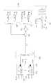
도 1은 본 발명의 일 실시예에 따른 WDM-PON 시스템을 도시한 블록도이다.1 is a block diagram illustrating a WDM-PON system according to an embodiment of the present invention.
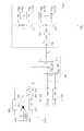
도면을 참조하면, 본 발명의 일 실시예에 따른 WDM-PON 시스템은, 씨앗광 모듈(100), 국사용 광장치(OLT,200), 원격 노드(RN, 300), 및 가입자 측 광단말장치(ONU, 400)를 포함한다. 도 1의 WDM-PON 시스템은, 스펙트럼 분할된 외부 광원모듈을 국사용 광장치(OLT) 광송신기의 씨앗광으로 사용하고, 하향데이터로 변조된 하향 광신호를 가입자 측 광단말장치(ONU)의 씨앗광으로 사용한다.Referring to the drawings, the WDM-PON system according to an embodiment of the present invention, the
씨앗광 모듈(100)은, 어븀(erbium)이 도핑(doping)된 광섬유(EDF, 140), 광섬유(EDF, 140)에게 외부광을 주입하여 캐리어를 생성시키는 펌프광원(Pump LD, 150), 펌프광원(Pump LD, 150)의 광을 광섬유(EDF, 140)으로 인입시키기 위한 광커플러(130), 광섬유(EDF, 140)로부터 왼쪽 방향으로 출력된 광대역 광을 스펙트럼 분할하는 광파장 역다중화기(112), 광파장 역다중화기(112)를 통해서 스펙트럼 분할된 광을 광파장 다중화하는 광파장 다중화기(111), 광파장 다중화기(111)로부터 출력된 광을 광섬유(EDF, 140) 방향으로 순환하고, 광섬유(EDF, 140)으로부터 왼쪽 방향으로 출력된 광을 광파장 역다중화기(112) 방향으로 순환시키는 광순환기(120)를 포함한다.
씨앗광 모듈(100)의 상세한 동작은 다음과 같다. 광섬유(EDF,140)에서는 왼쪽 및 오른쪽 양방향으로 자발 방출광이 출력된다. 넓은 파장 대역에서 연속적으로 출력되는 왼쪽방향 자발 방출광은, 광섬유(EDF,140) 앞단에 설치된 광순환기(120)의 2번 단자를 통해 입력되어 1번 단자를 통해 출력되고, 파장 역다중화/다중화 장치(112/111)에 의해 파장이 스펙트럼 분할/파장다중화된다. 다중화된 광은 광순환기(120)의 3번 단자로 입력된 후 광순환기(120)의 2번 단자를 통해 광섬유(EDF,140)로 입력된다. 광순환기(120)는 그 특성상 1번 단자로 입력된 빛은 2번 단자로만 출력되고, 2번 단자로 입력된 빛은 3번 단자로만 출력되며 그 반대방향으로는 출력되지 않는다.Detailed operation of the
파장 역다중화/다중화장치(112/111)는 다음과 같이 동작된다. 한 개의 단자 를 통해 입력된 광대역 광은 다수개의 출력단자를 통해 스펙트럼 분할되고, 스펙트럼 분할된 광은 다수개의 입력단자를 통해 입력된 후 파장 다중화가 되어 한 개의 단자로 출력된다.The wavelength demultiplexer /
역다중화/다중화 장치(112/111)는, 1xN 도파로형 회절격자(Arrayed-Waveguide Grating;AWG)나 박막 필터(Thin film filter; TFF)를 사용하여 구현할 수 있다. 파장 역다중화/다중화장치(112/111)는 목적에 따라 분할되는 스펙트럼 폭과 분할 개수가 달라질 수 있다. 또한 스펙트럼 분할 및 다중화하는 과정에서 각 채널별 연결 손실을 조절하여 출력된 신호들의 세기를 평탄화하는 기능을 수행할 수 있다.The demultiplexer /
한편, 왼쪽방향 자발 방출광을 광증폭기에 재입사하는 목적을 달성하기 위하여, 광순환기(120) 대신에 광을 일정비율로 분배하는 광분배기를 사용할 수도 있다. 하지만 가급적 재입사되는 역방향 자발방출광의 세기를 크게 유지해야하므로 손실이 적은 광순환기(120)를 사용하는 것이 바람직하다. 광섬유(EDF, 140) 증폭기에 재입사된 파장 분할된 자발방출광은 광증폭기의 입력신호처럼 동작하게 되어 효과적으로 증폭이 되어 오른쪽으로 출력된다. 광섬유 증폭기를 구성하는데 있어서, 펌프광원(Pump LD, 150)은 왼쪽방향 또는 오른쪽방향으로 각각 구성할 수 있으며, 왼쪽방향 및 오른쪽방향을 동시 구성할 수 있다.On the other hand, in order to achieve the purpose of re-incident left spontaneous emission light to the optical amplifier, instead of the
국사용 광장치(OLT, 200)는, 하향정보를 담고 있는 광신호를 송신하는 광송신기(210), 상향 광신호를 수신하는 광수신기(220), 서로 다른 파장으로 된 하향 광신호들을 파장 다중화하는 광파장 다중화기(231), 서로 다른 파장으로 된 상향 광신호들을 파장 분할하는 광파장 역다중화기(232), 씨앗광 모듈(100)로부터 수신된 광을 광파장 다중화기(231) 방향으로 순환시키고 광파장 다중화기(231)로부터 출력된 파장 다중화된 광신호들을 간선망(feeder fiber) 방향으로 순환시키는 제1 광순환기(240), 제1 광순환기(240)로부터 보내진 하향 광신호들을 간선망(feeder fiber)으로 순환하고 간선망(feeder fiber)에서 송신되는 상향 광신호들을 광파장 역다중화기(232) 방향으로 순환하는 제2 광순환기(250)를 포함한다.The national optical device (OLT) 200 has a wavelength multiplexed
국사용 광장치(OLT,200)의 상세 동작은 다음과 같다.Detailed operation of the national optical device (OLT, 200) is as follows.
씨앗광 모듈(100)로부터 스펙트럼 분할된 상태의 광은 제1 광순환기(240)의 1번 포트로 입력하여 2번 포트로 출력되고, 광파장 다중화기(231)의 출력포트로 입력되어 파장이 분할되고, 분할된 파장들은 각각 해당 광송신기(210-1,...,210-N)의 반사형 반도체 광증폭기(RSOA)에 입사된다. 반사형 반도체 광증폭기(RSOA)에 입사된 씨앗광은 증폭되고 하향데이터에 의해서 변조되어 반사형 반도체 광증폭기(RSOA)로부터 송신된다. 반사형 반도체 광증폭기(RSOA)에서 송신된 광은 광파장 다중화기(231)에서 다른 반사형 반도체 광증폭기(RSOA)들로부터 출력된 광신호들과 함께 파장 다중화된다. 광파장 다중화기(231)에서 출력된 파장 다중화된 광은, 제1 광순환기(240)의 2번 포트로 입력되어 3번 포트로 출력되고, 이어서 제2 광순환기(250)의 3번 포트로 입력되어 1번 포트로 출력되어 간선망(feeder fiber)으로 송신된다.The light in the spectrum split state from the
한편, 가입자 측에서 송신되는 파장다중화된 상향 광신호들은 제2 광순환기(250)의 1번 포트로 입력되어 2번 포트로 출력되고, 광파장 역다중화기(232)로 입력된다. 광파장 역다중화기(232)에 입력된 광신호들은 파장이 분리되어 각각의 파장은 해당 수신기(220-1,..., 220-N)로 입력되고, 수신기에서는 전기적인 신호(UN)로 변환된다.Meanwhile, the wavelength multiplexed uplink optical signals transmitted from the subscriber side are input to
원격 노드(RN, 300)는, 국사용 광장치(OLT)로부터 송신되는 파장 다중화된 하향 광신호들을 파장분리하고, 동시에 가입자 측 광단말장치(ONU, 400)들로부터 송신되는 서로 다른 광파장으로된 광신호들을 파장다중화 시키는 역할을 하는 광파장 다중화기(310)를 포함한다.The
가입자 측 광단말장치(ONU,400)는, 변조된 하향 광신호를 수신하여 하향 정보를 복구하는 광수신기(420), 하향 광신호를 수신하여 하향 정보를 제거하여 유사 연속(continuous wave;CW)광으로 변화시킨 후 이를 상향데이터로 변조하는 광송신기(410) 및 광커플러(430)를 포함한다.The subscriber side optical terminal device (ONU) 400 receives an modulated downlink optical signal to recover downlink information, and receives a downlink optical signal to remove downlink information to remove a similar continuous wave (CW). It includes an
가입자 측 광단말장치(ONU,400)의 상세 동작은 다음과 같다.Detailed operation of the subscriber-side optical terminal device (ONU, 400) is as follows.
원격 노드(RN,300)에서 송신되는 광신호는, 광커플러(430)에서 일부가 광송신기(410)로, 다른 일부는 광수신기(420)로 전달된다. 광송신기(410)에 포함된 반사형 반도체 광증폭기(RSOA)에 입력된 하향 광신호는 광적 및 전기적인 장치에 의해서 유사(Pseudo) CW(Continuous Wave) 광으로 변환되고, 변환된 광은 상향데이터로 변조되어 국사용 광장치(OLT, 200) 쪽으로 송신된다. 한편 광수신기(420)로 입력된 일부 광파워는 전기적인 신호로 변환되어 하향데이터가 복구된다.The optical signal transmitted from the
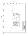
도 2는 종래의 WDM-PON 시스템과 도 1의 WDM-PON 시스템의 출력 스펙트럼을 비교 도시한 도면이다.FIG. 2 is a diagram comparing output spectra of a conventional WDM-PON system and the WDM-PON system of FIG. 1.
도면을 참조하여 설명하면, 도 2는, 종래의 광대역 광원(BLS)으로부터 출력되는 스펙트럼과, 도 1의 일실시예에 따른 WDM-PON 시스템의 씨앗광 모듈(100)로부터 출력되는 스펙트럼을 비교한다.Referring to the drawings, FIG. 2 compares the spectrum output from the conventional broadband light source (BLS) with the spectrum output from the
씨앗광 모듈(100)은 내부에서 스펙트럼을 분할하고, 각각의 스펙트럼을 다시 증폭한다. 국사용 광장치(OLT)에서 스펙트럼 분할 과정을 거칠 필요가 없으므로, 이에 의한 손실이 거의 없다. 따라서, 기존의 단순한 광대역 광원(BLS)에 비해서 출력이 획기적으로 증가된다. 또한, 씨앗광 모듈(100) 내부에 분할된 스펙트럼들 간의 파워를 균등하게 만들어 주는 기능을 손쉽게 실현 가능하므로, 필요시 균등한 광파워를 갖는 스펙트럼 분할된 광을 파장 다중화된 상태로 얻을 수 있다.The
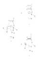
도 3(a) 내지 도 3(c)는 본 발명의 일 실시예에 따른 씨앗광 모듈을 도시한 블록도이다.3 (a) to 3 (c) is a block diagram showing a seed light module according to an embodiment of the present invention.
먼저, 도 3(a)의 씨앗광 모듈(100)은, 도 1의 광증폭 매질로서 어븀(erbium)이 도핑(doping)된 광섬유(EDF, 140) 대신, 다른 종류의 광섬유 증폭기들과 반도체 광증폭기(160)를 사용할 수 있다.First, the
즉, 광증폭기(160)는 외부광을 증폭하며, 광파장 역다중화기는 광증폭기로부터 왼쪽 방향으로 출력된 광대역 광을 스펙트럼 분할하고, 광파장 다중화기는 광파장 역다중화기를 통해서 스펙트럼 분할된 광을 광파장 다중화하며, 광순환기는 광파장 다중화기로부터 출력된 광을 광증폭기 방향으로 순환하고, 광증폭기로부터 왼쪽 방향으로 출력된 광을 광파장 역다중화기 방향으로 순환시킨다.That is, the
다음에, 도 3(b)의 씨앗광 모듈(100)은, 왼쪽방향 자발 방출광을 광섬 유(EDF, 140)에 재입력 시키는 방법에 있어서, 광파장 역다중화기(112)의 끝단에 고반사 코팅(170)을 함으로써, 광순환기(120)와 광파장 다중화기(111)를 대신하는 구조이다. 즉, 광파장 역다중화기(112)의 고반사 코팅(170)에 의해, 스펙트럼 분할된 광이 광파장 다중화된다.Next, the
다음에, 도 3(c)의 씨앗광 모듈(100)은, 스펙트럼 분할된 광의 출력 파워를 향상시키기 위하여 광섬유(EDF, 140)에 추가로 광증폭기(160)를 더 포함할 수 있다.Next, the
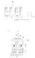
도 4는 본 발명의 일 실시예에 따른 WDM-PON 시스템을 도시한 블록도이다.4 is a block diagram illustrating a WDM-PON system according to an embodiment of the present invention.
도면을 참조하여 설명하면, 도 4의 WDM-PON 시스템은 도 1과 유사한 구조이다. 단, 도 1의 WDM-PON 시스템의 간선망(feeder fiber) 구간이 단일 광섬유인데 비해서, 도 4의 WDM-PON 시스템의 간선망(feeder fiber) 구간은 두 개의 광섬유로 이루어진다. 이를 위해서, 원격 노드(RN,300) 내에 광순환기(320)가 위치하여, 도 1의 제2 광순환기(250)의 역할을 하게 된다.Referring to the drawings, the WDM-PON system of FIG. 4 has a structure similar to that of FIG. However, the feeder fiber section of the WDM-PON system of FIG. 1 is a single optical fiber, whereas the feeder fiber section of the WDM-PON system of FIG. 4 is composed of two optical fibers. To this end, the
도 5(a) 내지 도 5(d)는 본 발명의 실시예에 따른 WDM-PON 시스템을 도시한 블록도이다.5 (a) to 5 (d) are block diagrams illustrating a WDM-PON system according to an embodiment of the present invention.
도면을 참조하여 설명하면, 도 5(a) 내지 도 5(d)의 본 발명의 실시예에 따른 WDM-PON 시스템은, 시분할 다중화 방식(TDMA) 가입자들을 수용할 수 있다. 즉, 도 5(a) 내지 도 5(d)의 WDM-PON 시스템은, 대부분 도 1의 WDM-PON 시스템과 유사하다. 다른 것은 원격 노드(RN,300)에 광파장 다중화기(310)에 추가로 파장별로 각각 광파워 분리기(330-1, ...,330-N)가 장착된다. 따라서, 광파장 다중화기(310)로 부터 파장분할된 하향 광신호는 광파워 분리기(330-1, ...,330-N)에서 파워가 분리되어 M개의 가입자 측 광단말장치(ONU,400)로 향하게 된다. 한편 M개의 가입자 측 광단말장치(ONU)로부터 송신된 상향 광신호는 광파워 분리기(330-1, ...,330-N)에서 모아져서 광파장 다중화기(310)으로 입력되고, 광파장 다중화기(310)에서 다른 파장의 광신호들과 파장 다중화 되어 국사용 광장치(OLT, 200)로 출력된다.Referring to the drawings, the WDM-PON system according to the embodiment of the present invention of FIGS. 5 (a) to 5 (d) may accommodate time division multiplexing (TDMA) subscribers. That is, the WDM-PON system of FIGS. 5A to 5D is mostly similar to the WDM-PON system of FIG. 1. Others are equipped with optical power separators 330-1, ..., 330-N for each wavelength in addition to the
먼저, 도 5(a)의 WDM-PON 시스템은, 간선망(feeder fiber) 구간이 단일 광섬유로 이루어진다. 따라서, 상향 및 하향 광신호를 분리하는 역할을 하는 제2 광순환기(250)가 국사용 광장치(OLT)에 위치한다.First, in the WDM-PON system of FIG. 5A, a feeder fiber section includes a single optical fiber. Therefore, the second
다음에, 도 5(b)의 WDM-PON 시스템은, 간선망(feeder fiber) 구간이 두 개의 분리된 광섬유로 이루어진다. 따라서, 상향 및 하향 광신호를 분리하는 역할을 하는 광순환기(320)가 원격 노드(RN)에 위치한다.Next, the WDM-PON system of FIG. 5 (b) consists of two separate optical fibers having a feeder fiber section. Accordingly, an
다음에, 도 5(c)의 WDM-PON 시스템은, 간선망(feeder fiber) 구간이 단일 광섬유로 이루어진다. 따라서, 상향 및 하향 광신호를 분리하는 역할을 하는 제2 광순환기(250)가 국사용 광장치(OLT)에 위치한다. 그리고, 광전송 거리를 늘리기 위해서 광증폭기(260) 및 (270)가 추가된다.Next, in the WDM-PON system of FIG. 5C, a feeder fiber section is formed of a single optical fiber. Therefore, the second
다음에, 도 5(d)의 WDM-PON 시스템은, 간선망(feeder fiber) 구간이 두 개의 분리된 광섬유로 이루어진다. 따라서, 상향 및 하향 광신호를 분리하는 역할을 하는 광순환기(320)가 원격 노드(RN)에 위치한다. 그리고, 광전송 거리를 늘리기 위해서 광증폭기(260) 및 (270)가 추가된다.Next, the WDM-PON system of FIG. 5 (d) includes two separate optical fibers having a feeder fiber section. Accordingly, an
도 6은 본 발명의 일 실시예에 따른 WDM-PON 시스템을 도시한 블록도이다.6 is a block diagram illustrating a WDM-PON system according to an embodiment of the present invention.
도면을 참조하여 설명하면, 도 6의 WDM-PON 시스템은, TDMA 가입자 측 광단말장치(ONU)를 교체 없이 그대로 사용할 수 있는 구조이다. 도 5와 다른 부분은 다음과 같다.Referring to the drawings, the WDM-PON system of FIG. 6 has a structure in which the TDMA subscriber-side optical terminal device ONU can be used as it is without replacement. A part different from FIG. 5 is as follows.
원격 노드(RN)는, 광필터(Optical Filter, 340)를 더 포함한다. 즉, 원격 노드(RN)는, 광파장 다중화기(310), 광파워 분리기(splitter, 330), 광필터(Optical Filter, 340)를 포함한다.The remote node RN further includes an
도 6의 WDM-PON 시스템은, 가입자 측에 위치하는 광파장 변환장치(500)를 더 포함한다.The WDM-PON system of FIG. 6 further includes an optical wavelength converter 500 located at the subscriber side.
광파장 변환장치(500)는, 제1 광필터(570), 제2 광필터(580), 제1 광수신기(510), 제2 광수신기(530), 제1 광송신기(560), 제2 광송신기(520), 양방향 증폭기(550), 및 광커플러(540)를 포함한다.The optical wavelength converter 500 includes a first
원격 노드(RN, 300) 및 가입자 측 장치(400, 500)의 동작은 다음과 같다.The operation of the
WDM 방식으로 전송된 하향 광신호들은 C-band 광파장들로 구성된다. 하향 광신호들은 광파장 다중화기(310)에서 파장분리되고, 파장분리된 광신호는 광필터(OF,340)의 1번 포트에 입력되어 3번 포트로 출력되고, 광파장 변환장치(500) 내에 위치하는 제1 광필터(570)의 1번 포트로 입력된다. 제1 광필터(570)의 1번 포트로 입력된 하향 광신호는 3번 포트로 출력되서, 제2 광필터(580)로 입력되고, 제2 광필터(580)의 2번 포트로 출력된다. 제2 광필터(580)의 2번 포트로 출력된 광신호는 양방향증폭기(550)에서 증폭되고, 광커플러(540)에서 광파워가 분리되어 일부는 제2 광송신기(520)의 반사형 반도체 광증폭기(RSOA)에 입력되고, 다른 일부는 제2 광수신기(530)로 입력되여 전기적인 신호로 변환된다. 제2 광수신기(530)에서 출력된 하향전기신호는 제1 광송신기(560)에 입력되어 TDM-PON의 하향 광신호 파장 대역과 일치하는 1490 nm 파장을 갖는 광신호로 변환되어 송신되고, 제1 광필터(570)의 제2 포트로 입력된다. 제1 광필터(570)의 제2포트로 입력된 1490 nm 파장의 하향 광신호는 제1 광필터(570)의 제1 포트로 출력되고, 원격 노드(RN,300) 내에 위치한 광필터(340)의 제3 포트로 입력되서, 광필터(340)의 2번 포트로 출력된다. 출력된 1490 nm 파장의 광신호는 광파워 분리기(splitter, 330)에서 광파워가 분리되어 M개의 가입자 측 광단말장치(ONU, 400)로 향한다.The downlink optical signals transmitted by the WDM scheme are composed of C-band optical wavelengths. The downlink optical signals are wavelength-separated by the
한편, M개의 가입자 측 광단말장치(ONU, 400)로부터 송신된 1310 nm 파장의 상향 광신호는 원격 노드(RN,300) 내의 광파워 분리기(splitter, 330)에서 모아져서 광필터(OF,340)의 2번 포트로 입력되서, 3번 포트로 출력된다. 1310 nm 파장의 상향 광신호는, 광파장 변환장치(500) 내의 제1 광필터(570)의 1번 포트로 입력되어 3번 포트로 출력되고, 제2 광필터(580)에 입력되어 1번 포트로 출력되고, 제1 광수신기(510)로 입력되어 전기적인 신호로 변환된다. 전기적인 상향신호는 제2 광송신기(520)의 반사형 반도체 광증폭기(RSOA)에 입력되어 하향 광신호의 파장을 갖는 광신호로 변환되어 출력된다. 한편, 광커플러(540)를 통해 반사형 반도체 광증폭기(RSOA,520)에 입력된 C-band 대역의 광파장을 갖는 하향 광신호는 제2 광송신기(520)에서 유사 CW 광으로 변환되어 상향광으로 사용된다. 반사형 반도체 광증폭기(RSOA, 520)로부터 출력된 상향 광신호는 양방향 증폭기(550)에서 증폭되어 제2 광필터(580)의 2번 포트로 입력되어 3번 포트로 출력되고, 제1 광필터(570)에 입력 되어 1번 포트로 출력된다. 광파장 변환장치(500)로부터 출력된 C-band 대역의 상향 광신호는 원격 노드(RN, 300) 내의 광필터(340)의 3번 포트로 입력되어 1번 포트로 출력되고, 광파장 다중화기(310)에서 다른 파장들을 갖는 상향신호들과 파장 다중화되어 국사용 광장치(OLT, 200)로 송신된다. 광파장 변환장치(500)에서의 양방향 증폭기(550)는 상향 및 하향 광신호의 전송거리에 따라 사용되지 않을 수 있다.On the other hand, the 1310 nm wavelength uplink optical signal transmitted from the M subscriber optical terminals (ONU, 400) is collected by the optical power splitter (330) in the remote node (RN, 300) and the optical filter (OF, 340). Input to
도 7은 도 6의 광파장 변환장치에서의 파장변환 전과 파장변환 후의 스펙트럼을 비교 도시한 도면이다. 도 7에서 세로축은 광파워를 나타낸다. 도면을 참조하여 설명하면, 도 7은, 도 6의 광파장 변환장치(500)에서의 파장변환 전의 상하향 광신호의 파장대역과 파장변환 후의 상하향 광신호의 파장대역의 스펙트럼을 비교한다.FIG. 7 is a diagram illustrating a comparison of the spectrum before and after wavelength conversion in the optical wavelength converter of FIG. 6. In Figure 7, the vertical axis represents optical power. Referring to the drawings, FIG. 7 compares the spectrum of the wavelength band of the up-down optical signal before the wavelength conversion and the wavelength band of the up-down optical signal after the wavelength conversion in the optical wavelength converter 500 of FIG.
1550 nm 근처의 파장을 가지는 상하향광 신호는, 도 6의 광파장 변환장치(500)에서 파장변환이 된 후에 1490 nm 파장의 하향 광신호와 1310 nm 파장의 상향 광신호로 변환이 된다. 이는 단지, 일예를 도시한 것으로 본 발명에서 제안한 구조와 목적하고자 하는 파장의 레이저 다이오드와 반사형 반도체 광증폭기를 구비한다면 어떠한 파장의 광도 원하는 파장으로 변환할 수 있다.The up-down light signal having a wavelength near 1550 nm is converted into a downlink optical signal having a wavelength of 1490 nm and an uplink optical signal having a wavelength of 1310 nm after the wavelength conversion is performed in the optical wavelength converter 500 of FIG. 6. This is merely an example, and if the structure proposed in the present invention and the laser diode and the reflective semiconductor optical amplifier of the desired wavelength are provided, the light of any wavelength can be converted into the desired wavelength.
도 8은 본 발명의 일 실시예에 따른 WDM-PON 시스템을 도시한 블록도이다.8 is a block diagram illustrating a WDM-PON system according to an embodiment of the present invention.
도면을 참조하여 설명하면, 도 8의 WDM-PON 시스템은, 가입자단의 가입자 측 광단말장치(ONU,400)를 광파장 변환장치(500)와 결합하여 사용하는 구조이다.Referring to the drawings, the WDM-PON system of FIG. 8 has a structure in which a subscriber side optical terminal device (ONU, 400) of a subscriber end is used in combination with an optical wavelength converter (500).
지정된 가입자 측 광단말장치(ONU, 400-1M)에서 송신된 1310 nm 파장의 상향 광신호는 제3 광필터(590)의 1번 포트로 입력되어 2번 포트로 출력되고, 광커플러(542)에 입력되어 제2 광필터(580)의 1번 포트에서 송신되는 1310 nm 파장의 다른 상향 광신호들과 합쳐져서 제1 광수신기(510)에 입력된다. 한편 제1 광송신기(560)에서 출력되는 1490 nm 파장의 하향 광신호는 광커플러(541)에서 광파워 분기되어 일부는 제1 광필터(570)의 2번 포트로 입력되고, 다른 일부는 제3 광필터(590)의 3번 포트로 입력되어 1번 포트로 출력되고, 지정된 가입자 측 광단말장치(ONU, 400-1M)로 입력되어 전기적인 신호로 변환된다.The 1310 nm wavelength uplink optical signal transmitted from the designated subscriber side optical terminal device (ONU, 400-1M) is input to
이상 첨부된 도면을 참조하여 본 발명의 실시예를 설명하였지만, 상술한 본 발명의 기술적 구성은 본 발명이 속하는 기술 분야의 당업자가 본 발명의 그 기술적 사상이나 필수적 특징을 변경하지 않고서 다른 구체적인 형태로 실시될 수 있다는 것을 이해할 수 있을 것이다. 그러므로 이상에서 기술한 실시 예들은 모든 면에서 예시적인 것이며 한정적인 것이 아닌 것으로서 이해되어야 한다. 아울러, 본 발명의 범위는 상기 상세한 설명보다는 후술하는 특허청구범위에 의하여 나타내어진다. 또한, 특허청구범위의 의미 및 범위 그리고 그 등가 개념으로부터 도출되는 모든 변경 또는 변형된 형태가 본 발명의 범위에 포함되는 것으로 해석되어야 한다.Although the embodiments of the present invention have been described above with reference to the accompanying drawings, the technical configuration of the present invention described above may be modified in other specific forms by those skilled in the art to which the present invention pertains without changing its technical spirit or essential features. It will be appreciated that it may be practiced. Therefore, the embodiments described above are to be understood as illustrative and not restrictive in all aspects. In addition, the scope of the present invention is shown by the claims below, rather than the above detailed description. Also, it is to be construed that all changes or modifications derived from the meaning and scope of the claims and their equivalent concepts are included in the scope of the present invention.
도 1은 본 발명의 일 실시예에 따른 WDM-PON 시스템을 도시한 블록도이다.1 is a block diagram illustrating a WDM-PON system according to an embodiment of the present invention.
도 2는 종래의 WDM-PON 시스템과 도 1의 WDM-PON 시스템의 출력 스펙트럼을 비교 도시한 도면이다.FIG. 2 is a diagram comparing output spectra of a conventional WDM-PON system and the WDM-PON system of FIG. 1.
도 3(a) 내지 도 3(c)는 본 발명의 일 실시예에 따른 씨앗광 모듈을 도시한 블록도이다.3 (a) to 3 (c) is a block diagram showing a seed light module according to an embodiment of the present invention.
도 4는 본 발명의 일 실시예에 따른 WDM-PON 시스템을 도시한 블록도이다.4 is a block diagram illustrating a WDM-PON system according to an embodiment of the present invention.
도 5(a) 내지 도 5(d)는 본 발명의 실시예에 따른 WDM-PON 시스템을 도시한 블록도이다.5 (a) to 5 (d) are block diagrams illustrating a WDM-PON system according to an embodiment of the present invention.
도 6은 본 발명의 일 실시예에 따른 WDM-PON 시스템을 도시한 블록도이다.6 is a block diagram illustrating a WDM-PON system according to an embodiment of the present invention.
도 7은 도 6의 광파장 변환장치에서의 파장변환 전과 파장변환 후의 스펙트럼을 비교 도시한 도면이다.FIG. 7 is a diagram illustrating a comparison of the spectrum before and after wavelength conversion in the optical wavelength converter of FIG. 6.
도 8은 본 발명의 일 실시예에 따른 WDM-PON 시스템을 도시한 블록도이다.8 is a block diagram illustrating a WDM-PON system according to an embodiment of the present invention.
<도면의 주요 부분에 관한 부호의 설명><Explanation of symbols on main parts of the drawings>
100:씨앗광모듈200:국사용 광장치100: seed optical module 200: optical device for national use
300:원격 노드400:가입자측 광단말장치300: remote node 400: subscriber side optical terminal device
500:광파장 변환장치500: light wavelength inverter
Claims (21)
Translated fromKoreanPriority Applications (5)
| Application Number | Priority Date | Filing Date | Title |
|---|---|---|---|
| KR1020070133784AKR100921797B1 (en) | 2007-12-18 | 2007-12-18 | Passive Optical Subscriber Network System with Wavelength Division Multiplexing |
| PCT/KR2008/006122WO2009078572A1 (en) | 2007-12-18 | 2008-10-16 | Wavelength division multiplexing-passive optical network system |
| US12/809,065US9008513B2 (en) | 2007-12-18 | 2008-10-16 | Wavelength division multiplexing-passive optical network system |
| CN2008801270091ACN101946430B (en) | 2007-12-18 | 2008-10-16 | Wavelength division multiplexing-passive optical network system |
| EP08862926AEP2241030A4 (en) | 2007-12-18 | 2008-10-16 | PASSIVE OPTICAL NETWORK SYSTEM WITH WAVELENGTH DIVISION MULTIPLEXING |
Applications Claiming Priority (1)
| Application Number | Priority Date | Filing Date | Title |
|---|---|---|---|
| KR1020070133784AKR100921797B1 (en) | 2007-12-18 | 2007-12-18 | Passive Optical Subscriber Network System with Wavelength Division Multiplexing |
Publications (2)
| Publication Number | Publication Date |
|---|---|
| KR20090066153A KR20090066153A (en) | 2009-06-23 |
| KR100921797B1true KR100921797B1 (en) | 2009-10-15 |
Family
ID=40795674
Family Applications (1)
| Application Number | Title | Priority Date | Filing Date |
|---|---|---|---|
| KR1020070133784AExpired - Fee RelatedKR100921797B1 (en) | 2007-12-18 | 2007-12-18 | Passive Optical Subscriber Network System with Wavelength Division Multiplexing |
Country Status (5)
| Country | Link |
|---|---|
| US (1) | US9008513B2 (en) |
| EP (1) | EP2241030A4 (en) |
| KR (1) | KR100921797B1 (en) |
| CN (1) | CN101946430B (en) |
| WO (1) | WO2009078572A1 (en) |
Cited By (1)
| Publication number | Priority date | Publication date | Assignee | Title |
|---|---|---|---|---|
| CN102959983A (en)* | 2010-08-27 | 2013-03-06 | 华为技术有限公司 | Passive optical network and device |
Families Citing this family (189)
| Publication number | Priority date | Publication date | Assignee | Title |
|---|---|---|---|---|
| US8364043B2 (en)* | 2008-12-12 | 2013-01-29 | Electronics And Telecommunications Research Institute | Method and apparatus for controlling reflective semiconductor optical amplifier (RSOA) |
| WO2011003481A1 (en)* | 2009-07-06 | 2011-01-13 | Telefonaktiebolaget Lm Ericsson (Publ) | Improvements in reflective optical networks |
| US8644708B2 (en)* | 2009-10-21 | 2014-02-04 | Futurewei Technologies | Coupled seed light injection for wavelength division multiplexing passive optical networks |
| KR101310455B1 (en)* | 2009-12-08 | 2013-09-24 | 한국전자통신연구원 | Wavelength division multiplexing passive optical network(wdm-pon) |
| NZ612254A (en)* | 2010-12-20 | 2014-12-24 | Ericsson Telefon Ab L M | Method and arrangement for receiving an optical input signal and transmitting an optical output signal |
| KR20120070260A (en)* | 2010-12-21 | 2012-06-29 | 한국전자통신연구원 | Seed light module for a passive optical network based on wavelength division multiplexing and driving method using the same |
| KR20120074357A (en)* | 2010-12-28 | 2012-07-06 | 한국전자통신연구원 | Passive optical network apparatus for transmitting optical signal |
| US9571187B2 (en) | 2011-05-25 | 2017-02-14 | Electronics And Telecommunications Research Institute | Wavelength-division multiplexing optical communication system and method for measuring optical performance of an output signal for the system |
| US9002214B2 (en) | 2011-07-14 | 2015-04-07 | Applied Optoelectronics, Inc. | Wavelength-selectable laser device and apparatus and system including same |
| US9502858B2 (en) | 2011-07-14 | 2016-11-22 | Applied Optoelectronics, Inc. | Laser array mux assembly with external reflector for providing a selected wavelength or multiplexed wavelengths |
| CN103703710B (en)* | 2011-07-29 | 2017-07-04 | 瑞典爱立信有限公司 | Optical access network |
| CN102412905B (en)* | 2011-11-10 | 2015-04-29 | 北京邮电大学 | Wavelength division-time division hybrid passive optical network system |
| KR20130126808A (en)* | 2012-04-24 | 2013-11-21 | 한국전자통신연구원 | Passive optical network system and method for transmitting and receiving optical signal thereof, and optical line terminal |
| US8953942B1 (en)* | 2012-04-27 | 2015-02-10 | Google Inc. | Hybrid WDM-TDM passive optical network |
| US9214790B2 (en)* | 2012-10-03 | 2015-12-15 | Applied Optoelectronics, Inc. | Filtered laser array assembly with external optical modulation and WDM optical system including same |
| US10009065B2 (en) | 2012-12-05 | 2018-06-26 | At&T Intellectual Property I, L.P. | Backhaul link for distributed antenna system |
| US9113347B2 (en) | 2012-12-05 | 2015-08-18 | At&T Intellectual Property I, Lp | Backhaul link for distributed antenna system |
| US9197352B2 (en)* | 2013-03-11 | 2015-11-24 | Google Inc. | Increasing the capacity of a WDM-PON with wavelength reuse |
| US9999038B2 (en) | 2013-05-31 | 2018-06-12 | At&T Intellectual Property I, L.P. | Remote distributed antenna system |
| US9525524B2 (en) | 2013-05-31 | 2016-12-20 | At&T Intellectual Property I, L.P. | Remote distributed antenna system |
| US9806817B2 (en)* | 2013-05-31 | 2017-10-31 | Telekom Malaysia Berhad | Wavelength division multiplexing passive optical network system |
| EP2830239B1 (en)* | 2013-07-23 | 2018-09-12 | ADVA Optical Networking SE | Method, system and transceiver device for bi-directionally transmitting digital optical signals over an optical transmission link |
| EP2854310B1 (en) | 2013-09-30 | 2017-07-12 | Alcatel Lucent | Optical line terminal for a passive optical wavelength division multiplex network |
| US8897697B1 (en) | 2013-11-06 | 2014-11-25 | At&T Intellectual Property I, Lp | Millimeter-wave surface-wave communications |
| US9209902B2 (en) | 2013-12-10 | 2015-12-08 | At&T Intellectual Property I, L.P. | Quasi-optical coupler |
| US9692101B2 (en) | 2014-08-26 | 2017-06-27 | At&T Intellectual Property I, L.P. | Guided wave couplers for coupling electromagnetic waves between a waveguide surface and a surface of a wire |
| CN104202091B (en)* | 2014-08-28 | 2019-03-08 | 昂纳信息技术(深圳)有限公司 | A photonic integrated optical module |
| US9768833B2 (en) | 2014-09-15 | 2017-09-19 | At&T Intellectual Property I, L.P. | Method and apparatus for sensing a condition in a transmission medium of electromagnetic waves |
| US10063280B2 (en) | 2014-09-17 | 2018-08-28 | At&T Intellectual Property I, L.P. | Monitoring and mitigating conditions in a communication network |
| US9628854B2 (en) | 2014-09-29 | 2017-04-18 | At&T Intellectual Property I, L.P. | Method and apparatus for distributing content in a communication network |
| US9615269B2 (en) | 2014-10-02 | 2017-04-04 | At&T Intellectual Property I, L.P. | Method and apparatus that provides fault tolerance in a communication network |
| US9685992B2 (en) | 2014-10-03 | 2017-06-20 | At&T Intellectual Property I, L.P. | Circuit panel network and methods thereof |
| US9503189B2 (en) | 2014-10-10 | 2016-11-22 | At&T Intellectual Property I, L.P. | Method and apparatus for arranging communication sessions in a communication system |
| US9973299B2 (en) | 2014-10-14 | 2018-05-15 | At&T Intellectual Property I, L.P. | Method and apparatus for adjusting a mode of communication in a communication network |
| US9762289B2 (en) | 2014-10-14 | 2017-09-12 | At&T Intellectual Property I, L.P. | Method and apparatus for transmitting or receiving signals in a transportation system |
| US9769020B2 (en) | 2014-10-21 | 2017-09-19 | At&T Intellectual Property I, L.P. | Method and apparatus for responding to events affecting communications in a communication network |
| US9653770B2 (en) | 2014-10-21 | 2017-05-16 | At&T Intellectual Property I, L.P. | Guided wave coupler, coupling module and methods for use therewith |
| US9312919B1 (en) | 2014-10-21 | 2016-04-12 | At&T Intellectual Property I, Lp | Transmission device with impairment compensation and methods for use therewith |
| US9564947B2 (en) | 2014-10-21 | 2017-02-07 | At&T Intellectual Property I, L.P. | Guided-wave transmission device with diversity and methods for use therewith |
| US9577306B2 (en) | 2014-10-21 | 2017-02-21 | At&T Intellectual Property I, L.P. | Guided-wave transmission device and methods for use therewith |
| US9780834B2 (en) | 2014-10-21 | 2017-10-03 | At&T Intellectual Property I, L.P. | Method and apparatus for transmitting electromagnetic waves |
| US9520945B2 (en) | 2014-10-21 | 2016-12-13 | At&T Intellectual Property I, L.P. | Apparatus for providing communication services and methods thereof |
| US9627768B2 (en) | 2014-10-21 | 2017-04-18 | At&T Intellectual Property I, L.P. | Guided-wave transmission device with non-fundamental mode propagation and methods for use therewith |
| US9742462B2 (en) | 2014-12-04 | 2017-08-22 | At&T Intellectual Property I, L.P. | Transmission medium and communication interfaces and methods for use therewith |
| US9954287B2 (en) | 2014-11-20 | 2018-04-24 | At&T Intellectual Property I, L.P. | Apparatus for converting wireless signals and electromagnetic waves and methods thereof |
| US9544006B2 (en) | 2014-11-20 | 2017-01-10 | At&T Intellectual Property I, L.P. | Transmission device with mode division multiplexing and methods for use therewith |
| US9997819B2 (en) | 2015-06-09 | 2018-06-12 | At&T Intellectual Property I, L.P. | Transmission medium and method for facilitating propagation of electromagnetic waves via a core |
| US10243784B2 (en) | 2014-11-20 | 2019-03-26 | At&T Intellectual Property I, L.P. | System for generating topology information and methods thereof |
| US9654173B2 (en) | 2014-11-20 | 2017-05-16 | At&T Intellectual Property I, L.P. | Apparatus for powering a communication device and methods thereof |
| US9680670B2 (en) | 2014-11-20 | 2017-06-13 | At&T Intellectual Property I, L.P. | Transmission device with channel equalization and control and methods for use therewith |
| US10009067B2 (en) | 2014-12-04 | 2018-06-26 | At&T Intellectual Property I, L.P. | Method and apparatus for configuring a communication interface |
| US9461706B1 (en) | 2015-07-31 | 2016-10-04 | At&T Intellectual Property I, Lp | Method and apparatus for exchanging communication signals |
| US10340573B2 (en) | 2016-10-26 | 2019-07-02 | At&T Intellectual Property I, L.P. | Launcher with cylindrical coupling device and methods for use therewith |
| US9800327B2 (en) | 2014-11-20 | 2017-10-24 | At&T Intellectual Property I, L.P. | Apparatus for controlling operations of a communication device and methods thereof |
| US10144036B2 (en) | 2015-01-30 | 2018-12-04 | At&T Intellectual Property I, L.P. | Method and apparatus for mitigating interference affecting a propagation of electromagnetic waves guided by a transmission medium |
| US9876570B2 (en) | 2015-02-20 | 2018-01-23 | At&T Intellectual Property I, Lp | Guided-wave transmission device with non-fundamental mode propagation and methods for use therewith |
| US9749013B2 (en) | 2015-03-17 | 2017-08-29 | At&T Intellectual Property I, L.P. | Method and apparatus for reducing attenuation of electromagnetic waves guided by a transmission medium |
| US10224981B2 (en) | 2015-04-24 | 2019-03-05 | At&T Intellectual Property I, Lp | Passive electrical coupling device and methods for use therewith |
| US9705561B2 (en) | 2015-04-24 | 2017-07-11 | At&T Intellectual Property I, L.P. | Directional coupling device and methods for use therewith |
| US9793954B2 (en) | 2015-04-28 | 2017-10-17 | At&T Intellectual Property I, L.P. | Magnetic coupling device and methods for use therewith |
| US9948354B2 (en) | 2015-04-28 | 2018-04-17 | At&T Intellectual Property I, L.P. | Magnetic coupling device with reflective plate and methods for use therewith |
| US9748626B2 (en) | 2015-05-14 | 2017-08-29 | At&T Intellectual Property I, L.P. | Plurality of cables having different cross-sectional shapes which are bundled together to form a transmission medium |
| US9490869B1 (en) | 2015-05-14 | 2016-11-08 | At&T Intellectual Property I, L.P. | Transmission medium having multiple cores and methods for use therewith |
| US9871282B2 (en) | 2015-05-14 | 2018-01-16 | At&T Intellectual Property I, L.P. | At least one transmission medium having a dielectric surface that is covered at least in part by a second dielectric |
| US10650940B2 (en) | 2015-05-15 | 2020-05-12 | At&T Intellectual Property I, L.P. | Transmission medium having a conductive material and methods for use therewith |
| US10679767B2 (en) | 2015-05-15 | 2020-06-09 | At&T Intellectual Property I, L.P. | Transmission medium having a conductive material and methods for use therewith |
| US9917341B2 (en) | 2015-05-27 | 2018-03-13 | At&T Intellectual Property I, L.P. | Apparatus and method for launching electromagnetic waves and for modifying radial dimensions of the propagating electromagnetic waves |
| US9866309B2 (en) | 2015-06-03 | 2018-01-09 | At&T Intellectual Property I, Lp | Host node device and methods for use therewith |
| US10812174B2 (en) | 2015-06-03 | 2020-10-20 | At&T Intellectual Property I, L.P. | Client node device and methods for use therewith |
| US10348391B2 (en) | 2015-06-03 | 2019-07-09 | At&T Intellectual Property I, L.P. | Client node device with frequency conversion and methods for use therewith |
| US10103801B2 (en) | 2015-06-03 | 2018-10-16 | At&T Intellectual Property I, L.P. | Host node device and methods for use therewith |
| US9912381B2 (en) | 2015-06-03 | 2018-03-06 | At&T Intellectual Property I, Lp | Network termination and methods for use therewith |
| US10154493B2 (en) | 2015-06-03 | 2018-12-11 | At&T Intellectual Property I, L.P. | Network termination and methods for use therewith |
| US9913139B2 (en) | 2015-06-09 | 2018-03-06 | At&T Intellectual Property I, L.P. | Signal fingerprinting for authentication of communicating devices |
| US9608692B2 (en) | 2015-06-11 | 2017-03-28 | At&T Intellectual Property I, L.P. | Repeater and methods for use therewith |
| US10142086B2 (en) | 2015-06-11 | 2018-11-27 | At&T Intellectual Property I, L.P. | Repeater and methods for use therewith |
| US9820146B2 (en) | 2015-06-12 | 2017-11-14 | At&T Intellectual Property I, L.P. | Method and apparatus for authentication and identity management of communicating devices |
| US9667317B2 (en) | 2015-06-15 | 2017-05-30 | At&T Intellectual Property I, L.P. | Method and apparatus for providing security using network traffic adjustments |
| US9865911B2 (en) | 2015-06-25 | 2018-01-09 | At&T Intellectual Property I, L.P. | Waveguide system for slot radiating first electromagnetic waves that are combined into a non-fundamental wave mode second electromagnetic wave on a transmission medium |
| US9640850B2 (en) | 2015-06-25 | 2017-05-02 | At&T Intellectual Property I, L.P. | Methods and apparatus for inducing a non-fundamental wave mode on a transmission medium |
| US9509415B1 (en) | 2015-06-25 | 2016-11-29 | At&T Intellectual Property I, L.P. | Methods and apparatus for inducing a fundamental wave mode on a transmission medium |
| US10044409B2 (en) | 2015-07-14 | 2018-08-07 | At&T Intellectual Property I, L.P. | Transmission medium and methods for use therewith |
| US10320586B2 (en) | 2015-07-14 | 2019-06-11 | At&T Intellectual Property I, L.P. | Apparatus and methods for generating non-interfering electromagnetic waves on an insulated transmission medium |
| US9722318B2 (en) | 2015-07-14 | 2017-08-01 | At&T Intellectual Property I, L.P. | Method and apparatus for coupling an antenna to a device |
| US10205655B2 (en) | 2015-07-14 | 2019-02-12 | At&T Intellectual Property I, L.P. | Apparatus and methods for communicating utilizing an antenna array and multiple communication paths |
| US9628116B2 (en) | 2015-07-14 | 2017-04-18 | At&T Intellectual Property I, L.P. | Apparatus and methods for transmitting wireless signals |
| US10033108B2 (en) | 2015-07-14 | 2018-07-24 | At&T Intellectual Property I, L.P. | Apparatus and methods for generating an electromagnetic wave having a wave mode that mitigates interference |
| US9847566B2 (en) | 2015-07-14 | 2017-12-19 | At&T Intellectual Property I, L.P. | Method and apparatus for adjusting a field of a signal to mitigate interference |
| US10341142B2 (en) | 2015-07-14 | 2019-07-02 | At&T Intellectual Property I, L.P. | Apparatus and methods for generating non-interfering electromagnetic waves on an uninsulated conductor |
| US10170840B2 (en) | 2015-07-14 | 2019-01-01 | At&T Intellectual Property I, L.P. | Apparatus and methods for sending or receiving electromagnetic signals |
| US10033107B2 (en) | 2015-07-14 | 2018-07-24 | At&T Intellectual Property I, L.P. | Method and apparatus for coupling an antenna to a device |
| US9882257B2 (en) | 2015-07-14 | 2018-01-30 | At&T Intellectual Property I, L.P. | Method and apparatus for launching a wave mode that mitigates interference |
| US9836957B2 (en) | 2015-07-14 | 2017-12-05 | At&T Intellectual Property I, L.P. | Method and apparatus for communicating with premises equipment |
| US10148016B2 (en) | 2015-07-14 | 2018-12-04 | At&T Intellectual Property I, L.P. | Apparatus and methods for communicating utilizing an antenna array |
| US9853342B2 (en) | 2015-07-14 | 2017-12-26 | At&T Intellectual Property I, L.P. | Dielectric transmission medium connector and methods for use therewith |
| US9793951B2 (en) | 2015-07-15 | 2017-10-17 | At&T Intellectual Property I, L.P. | Method and apparatus for launching a wave mode that mitigates interference |
| US9608740B2 (en) | 2015-07-15 | 2017-03-28 | At&T Intellectual Property I, L.P. | Method and apparatus for launching a wave mode that mitigates interference |
| US10090606B2 (en) | 2015-07-15 | 2018-10-02 | At&T Intellectual Property I, L.P. | Antenna system with dielectric array and methods for use therewith |
| US9749053B2 (en) | 2015-07-23 | 2017-08-29 | At&T Intellectual Property I, L.P. | Node device, repeater and methods for use therewith |
| US10784670B2 (en) | 2015-07-23 | 2020-09-22 | At&T Intellectual Property I, L.P. | Antenna support for aligning an antenna |
| US9912027B2 (en) | 2015-07-23 | 2018-03-06 | At&T Intellectual Property I, L.P. | Method and apparatus for exchanging communication signals |
| US9871283B2 (en) | 2015-07-23 | 2018-01-16 | At&T Intellectual Property I, Lp | Transmission medium having a dielectric core comprised of plural members connected by a ball and socket configuration |
| US9948333B2 (en) | 2015-07-23 | 2018-04-17 | At&T Intellectual Property I, L.P. | Method and apparatus for wireless communications to mitigate interference |
| US10020587B2 (en) | 2015-07-31 | 2018-07-10 | At&T Intellectual Property I, L.P. | Radial antenna and methods for use therewith |
| US9967173B2 (en) | 2015-07-31 | 2018-05-08 | At&T Intellectual Property I, L.P. | Method and apparatus for authentication and identity management of communicating devices |
| US9735833B2 (en) | 2015-07-31 | 2017-08-15 | At&T Intellectual Property I, L.P. | Method and apparatus for communications management in a neighborhood network |
| US9904535B2 (en) | 2015-09-14 | 2018-02-27 | At&T Intellectual Property I, L.P. | Method and apparatus for distributing software |
| US10136434B2 (en) | 2015-09-16 | 2018-11-20 | At&T Intellectual Property I, L.P. | Method and apparatus for use with a radio distributed antenna system having an ultra-wideband control channel |
| US10051629B2 (en) | 2015-09-16 | 2018-08-14 | At&T Intellectual Property I, L.P. | Method and apparatus for use with a radio distributed antenna system having an in-band reference signal |
| US9705571B2 (en) | 2015-09-16 | 2017-07-11 | At&T Intellectual Property I, L.P. | Method and apparatus for use with a radio distributed antenna system |
| US10009901B2 (en) | 2015-09-16 | 2018-06-26 | At&T Intellectual Property I, L.P. | Method, apparatus, and computer-readable storage medium for managing utilization of wireless resources between base stations |
| US10079661B2 (en) | 2015-09-16 | 2018-09-18 | At&T Intellectual Property I, L.P. | Method and apparatus for use with a radio distributed antenna system having a clock reference |
| US10009063B2 (en) | 2015-09-16 | 2018-06-26 | At&T Intellectual Property I, L.P. | Method and apparatus for use with a radio distributed antenna system having an out-of-band reference signal |
| US9769128B2 (en) | 2015-09-28 | 2017-09-19 | At&T Intellectual Property I, L.P. | Method and apparatus for encryption of communications over a network |
| US9729197B2 (en) | 2015-10-01 | 2017-08-08 | At&T Intellectual Property I, L.P. | Method and apparatus for communicating network management traffic over a network |
| US9876264B2 (en) | 2015-10-02 | 2018-01-23 | At&T Intellectual Property I, Lp | Communication system, guided wave switch and methods for use therewith |
| US10074890B2 (en) | 2015-10-02 | 2018-09-11 | At&T Intellectual Property I, L.P. | Communication device and antenna with integrated light assembly |
| US9882277B2 (en) | 2015-10-02 | 2018-01-30 | At&T Intellectual Property I, Lp | Communication device and antenna assembly with actuated gimbal mount |
| US10051483B2 (en) | 2015-10-16 | 2018-08-14 | At&T Intellectual Property I, L.P. | Method and apparatus for directing wireless signals |
| US10665942B2 (en) | 2015-10-16 | 2020-05-26 | At&T Intellectual Property I, L.P. | Method and apparatus for adjusting wireless communications |
| US10355367B2 (en) | 2015-10-16 | 2019-07-16 | At&T Intellectual Property I, L.P. | Antenna structure for exchanging wireless signals |
| US9749080B2 (en)* | 2015-11-11 | 2017-08-29 | Google Inc. | TWDM passive network with extended reach and capacity |
| US9912419B1 (en) | 2016-08-24 | 2018-03-06 | At&T Intellectual Property I, L.P. | Method and apparatus for managing a fault in a distributed antenna system |
| US9860075B1 (en) | 2016-08-26 | 2018-01-02 | At&T Intellectual Property I, L.P. | Method and communication node for broadband distribution |
| US10291311B2 (en) | 2016-09-09 | 2019-05-14 | At&T Intellectual Property I, L.P. | Method and apparatus for mitigating a fault in a distributed antenna system |
| US11032819B2 (en) | 2016-09-15 | 2021-06-08 | At&T Intellectual Property I, L.P. | Method and apparatus for use with a radio distributed antenna system having a control channel reference signal |
| US10340600B2 (en) | 2016-10-18 | 2019-07-02 | At&T Intellectual Property I, L.P. | Apparatus and methods for launching guided waves via plural waveguide systems |
| US10135146B2 (en) | 2016-10-18 | 2018-11-20 | At&T Intellectual Property I, L.P. | Apparatus and methods for launching guided waves via circuits |
| US10135147B2 (en) | 2016-10-18 | 2018-11-20 | At&T Intellectual Property I, L.P. | Apparatus and methods for launching guided waves via an antenna |
| US10811767B2 (en) | 2016-10-21 | 2020-10-20 | At&T Intellectual Property I, L.P. | System and dielectric antenna with convex dielectric radome |
| US10374316B2 (en) | 2016-10-21 | 2019-08-06 | At&T Intellectual Property I, L.P. | System and dielectric antenna with non-uniform dielectric |
| US9991580B2 (en) | 2016-10-21 | 2018-06-05 | At&T Intellectual Property I, L.P. | Launcher and coupling system for guided wave mode cancellation |
| US9876605B1 (en) | 2016-10-21 | 2018-01-23 | At&T Intellectual Property I, L.P. | Launcher and coupling system to support desired guided wave mode |
| US10312567B2 (en) | 2016-10-26 | 2019-06-04 | At&T Intellectual Property I, L.P. | Launcher with planar strip antenna and methods for use therewith |
| US10498044B2 (en) | 2016-11-03 | 2019-12-03 | At&T Intellectual Property I, L.P. | Apparatus for configuring a surface of an antenna |
| US10224634B2 (en) | 2016-11-03 | 2019-03-05 | At&T Intellectual Property I, L.P. | Methods and apparatus for adjusting an operational characteristic of an antenna |
| US10225025B2 (en) | 2016-11-03 | 2019-03-05 | At&T Intellectual Property I, L.P. | Method and apparatus for detecting a fault in a communication system |
| US10291334B2 (en) | 2016-11-03 | 2019-05-14 | At&T Intellectual Property I, L.P. | System for detecting a fault in a communication system |
| US10340603B2 (en) | 2016-11-23 | 2019-07-02 | At&T Intellectual Property I, L.P. | Antenna system having shielded structural configurations for assembly |
| US10178445B2 (en) | 2016-11-23 | 2019-01-08 | At&T Intellectual Property I, L.P. | Methods, devices, and systems for load balancing between a plurality of waveguides |
| US10090594B2 (en) | 2016-11-23 | 2018-10-02 | At&T Intellectual Property I, L.P. | Antenna system having structural configurations for assembly |
| US10535928B2 (en) | 2016-11-23 | 2020-01-14 | At&T Intellectual Property I, L.P. | Antenna system and methods for use therewith |
| US10340601B2 (en) | 2016-11-23 | 2019-07-02 | At&T Intellectual Property I, L.P. | Multi-antenna system and methods for use therewith |
| US10361489B2 (en) | 2016-12-01 | 2019-07-23 | At&T Intellectual Property I, L.P. | Dielectric dish antenna system and methods for use therewith |
| US10305190B2 (en) | 2016-12-01 | 2019-05-28 | At&T Intellectual Property I, L.P. | Reflecting dielectric antenna system and methods for use therewith |
| US9927517B1 (en) | 2016-12-06 | 2018-03-27 | At&T Intellectual Property I, L.P. | Apparatus and methods for sensing rainfall |
| US10020844B2 (en) | 2016-12-06 | 2018-07-10 | T&T Intellectual Property I, L.P. | Method and apparatus for broadcast communication via guided waves |
| US10439675B2 (en) | 2016-12-06 | 2019-10-08 | At&T Intellectual Property I, L.P. | Method and apparatus for repeating guided wave communication signals |
| US10819035B2 (en) | 2016-12-06 | 2020-10-27 | At&T Intellectual Property I, L.P. | Launcher with helical antenna and methods for use therewith |
| US10727599B2 (en) | 2016-12-06 | 2020-07-28 | At&T Intellectual Property I, L.P. | Launcher with slot antenna and methods for use therewith |
| US10694379B2 (en) | 2016-12-06 | 2020-06-23 | At&T Intellectual Property I, L.P. | Waveguide system with device-based authentication and methods for use therewith |
| US10326494B2 (en) | 2016-12-06 | 2019-06-18 | At&T Intellectual Property I, L.P. | Apparatus for measurement de-embedding and methods for use therewith |
| US10135145B2 (en) | 2016-12-06 | 2018-11-20 | At&T Intellectual Property I, L.P. | Apparatus and methods for generating an electromagnetic wave along a transmission medium |
| US10382976B2 (en) | 2016-12-06 | 2019-08-13 | At&T Intellectual Property I, L.P. | Method and apparatus for managing wireless communications based on communication paths and network device positions |
| US10637149B2 (en) | 2016-12-06 | 2020-04-28 | At&T Intellectual Property I, L.P. | Injection molded dielectric antenna and methods for use therewith |
| US10755542B2 (en) | 2016-12-06 | 2020-08-25 | At&T Intellectual Property I, L.P. | Method and apparatus for surveillance via guided wave communication |
| US9893795B1 (en) | 2016-12-07 | 2018-02-13 | At&T Intellectual Property I, Lp | Method and repeater for broadband distribution |
| US10243270B2 (en) | 2016-12-07 | 2019-03-26 | At&T Intellectual Property I, L.P. | Beam adaptive multi-feed dielectric antenna system and methods for use therewith |
| US10168695B2 (en) | 2016-12-07 | 2019-01-01 | At&T Intellectual Property I, L.P. | Method and apparatus for controlling an unmanned aircraft |
| US10139820B2 (en) | 2016-12-07 | 2018-11-27 | At&T Intellectual Property I, L.P. | Method and apparatus for deploying equipment of a communication system |
| US10547348B2 (en) | 2016-12-07 | 2020-01-28 | At&T Intellectual Property I, L.P. | Method and apparatus for switching transmission mediums in a communication system |
| US10027397B2 (en) | 2016-12-07 | 2018-07-17 | At&T Intellectual Property I, L.P. | Distributed antenna system and methods for use therewith |
| US10389029B2 (en) | 2016-12-07 | 2019-08-20 | At&T Intellectual Property I, L.P. | Multi-feed dielectric antenna system with core selection and methods for use therewith |
| US10359749B2 (en) | 2016-12-07 | 2019-07-23 | At&T Intellectual Property I, L.P. | Method and apparatus for utilities management via guided wave communication |
| US10446936B2 (en) | 2016-12-07 | 2019-10-15 | At&T Intellectual Property I, L.P. | Multi-feed dielectric antenna system and methods for use therewith |
| US10326689B2 (en) | 2016-12-08 | 2019-06-18 | At&T Intellectual Property I, L.P. | Method and system for providing alternative communication paths |
| US10916969B2 (en) | 2016-12-08 | 2021-02-09 | At&T Intellectual Property I, L.P. | Method and apparatus for providing power using an inductive coupling |
| US10777873B2 (en) | 2016-12-08 | 2020-09-15 | At&T Intellectual Property I, L.P. | Method and apparatus for mounting network devices |
| US9998870B1 (en) | 2016-12-08 | 2018-06-12 | At&T Intellectual Property I, L.P. | Method and apparatus for proximity sensing |
| US10103422B2 (en) | 2016-12-08 | 2018-10-16 | At&T Intellectual Property I, L.P. | Method and apparatus for mounting network devices |
| US10069535B2 (en) | 2016-12-08 | 2018-09-04 | At&T Intellectual Property I, L.P. | Apparatus and methods for launching electromagnetic waves having a certain electric field structure |
| US10601494B2 (en) | 2016-12-08 | 2020-03-24 | At&T Intellectual Property I, L.P. | Dual-band communication device and method for use therewith |
| US10938108B2 (en) | 2016-12-08 | 2021-03-02 | At&T Intellectual Property I, L.P. | Frequency selective multi-feed dielectric antenna system and methods for use therewith |
| US9911020B1 (en) | 2016-12-08 | 2018-03-06 | At&T Intellectual Property I, L.P. | Method and apparatus for tracking via a radio frequency identification device |
| US10411356B2 (en) | 2016-12-08 | 2019-09-10 | At&T Intellectual Property I, L.P. | Apparatus and methods for selectively targeting communication devices with an antenna array |
| US10530505B2 (en) | 2016-12-08 | 2020-01-07 | At&T Intellectual Property I, L.P. | Apparatus and methods for launching electromagnetic waves along a transmission medium |
| US10389037B2 (en) | 2016-12-08 | 2019-08-20 | At&T Intellectual Property I, L.P. | Apparatus and methods for selecting sections of an antenna array and use therewith |
| US10264586B2 (en) | 2016-12-09 | 2019-04-16 | At&T Mobility Ii Llc | Cloud-based packet controller and methods for use therewith |
| US9838896B1 (en) | 2016-12-09 | 2017-12-05 | At&T Intellectual Property I, L.P. | Method and apparatus for assessing network coverage |
| US10340983B2 (en) | 2016-12-09 | 2019-07-02 | At&T Intellectual Property I, L.P. | Method and apparatus for surveying remote sites via guided wave communications |
| US10564512B2 (en) | 2017-02-03 | 2020-02-18 | The George Washington University | Hybrid photonic non-blocking wide spectrum WDM on-chip router |
| US9973940B1 (en) | 2017-02-27 | 2018-05-15 | At&T Intellectual Property I, L.P. | Apparatus and methods for dynamic impedance matching of a guided wave launcher |
| US10298293B2 (en) | 2017-03-13 | 2019-05-21 | At&T Intellectual Property I, L.P. | Apparatus of communication utilizing wireless network devices |
| CN110798265A (en)* | 2018-08-01 | 2020-02-14 | 中兴通讯股份有限公司 | Optical module, method, device and system for obtaining optical signal and storage medium |
| CN111107450A (en)* | 2018-10-26 | 2020-05-05 | 中兴通讯股份有限公司 | Method and device for realizing OLT slicing |
| US10812136B1 (en) | 2019-12-02 | 2020-10-20 | At&T Intellectual Property I, L.P. | Surface wave repeater with controllable isolator and methods for use therewith |
| CN112671502A (en)* | 2020-12-28 | 2021-04-16 | 武汉光迅科技股份有限公司 | Optical line terminal |
| US12316375B2 (en)* | 2023-06-01 | 2025-05-27 | King Fahd University Of Petroleum And Minerals | Bi-directional optical communication system |
| CN118984189A (en)* | 2024-01-05 | 2024-11-19 | 华为技术有限公司 | Optical communication system, method, related device, storage medium and program product |
Citations (2)
| Publication number | Priority date | Publication date | Assignee | Title |
|---|---|---|---|---|
| KR20060100127A (en)* | 2005-03-16 | 2006-09-20 | 주식회사 케이티 | Wavelength Division Multiplexed Transmission System Using Shared Seed Light Source |
| KR20070109768A (en)* | 2006-05-11 | 2007-11-15 | 한국전자통신연구원 | Passive Optical Subscriber Network Based on Reflective Semiconductor Optical Amplifier |
Family Cites Families (8)
| Publication number | Priority date | Publication date | Assignee | Title |
|---|---|---|---|---|
| US20030007207A1 (en) | 2001-04-21 | 2003-01-09 | Peter Healey | Optical signal transmitter |
| US20030007202A1 (en)* | 2001-05-09 | 2003-01-09 | Ondax, Inc. | Microelectromechanical system (MEMS) based tunable hitless add-drop filter |
| GB0311563D0 (en)* | 2003-05-20 | 2003-06-25 | Nokia Corp | Optical data transmission system |
| KR100575983B1 (en)* | 2003-08-23 | 2006-05-02 | 삼성전자주식회사 | Multiwavelength Optical Transmitter and Bidirectional Wavelength Division Multiplexing |
| KR100575966B1 (en)* | 2003-12-18 | 2006-05-02 | 삼성전자주식회사 | Broadband light source |
| KR100606028B1 (en)* | 2004-07-07 | 2006-07-31 | 삼성전자주식회사 | Light source and optical communication system for wavelength division multiplex optical communication |
| KR100678245B1 (en)* | 2004-12-01 | 2007-02-02 | 삼성전자주식회사 | Passive Optical Subscriber Network |
| KR100720113B1 (en)* | 2005-08-29 | 2007-05-18 | 한국과학기술원 | The wavelength-division multiplexed passive optical network for reducing the degraded noise performance of wavelength-locked Fabry-Perot laser diodes |
- 2007
- 2007-12-18KRKR1020070133784Apatent/KR100921797B1/ennot_activeExpired - Fee Related
- 2008
- 2008-10-16USUS12/809,065patent/US9008513B2/enactiveActive
- 2008-10-16EPEP08862926Apatent/EP2241030A4/ennot_activeWithdrawn
- 2008-10-16CNCN2008801270091Apatent/CN101946430B/ennot_activeExpired - Fee Related
- 2008-10-16WOPCT/KR2008/006122patent/WO2009078572A1/enactiveApplication Filing
Patent Citations (2)
| Publication number | Priority date | Publication date | Assignee | Title |
|---|---|---|---|---|
| KR20060100127A (en)* | 2005-03-16 | 2006-09-20 | 주식회사 케이티 | Wavelength Division Multiplexed Transmission System Using Shared Seed Light Source |
| KR20070109768A (en)* | 2006-05-11 | 2007-11-15 | 한국전자통신연구원 | Passive Optical Subscriber Network Based on Reflective Semiconductor Optical Amplifier |
Cited By (2)
| Publication number | Priority date | Publication date | Assignee | Title |
|---|---|---|---|---|
| CN102959983A (en)* | 2010-08-27 | 2013-03-06 | 华为技术有限公司 | Passive optical network and device |
| CN102959983B (en)* | 2010-08-27 | 2015-07-08 | 华为技术有限公司 | Passive optical network systems and equipment |
Also Published As
| Publication number | Publication date |
|---|---|
| CN101946430A (en) | 2011-01-12 |
| CN101946430B (en) | 2013-10-30 |
| KR20090066153A (en) | 2009-06-23 |
| US9008513B2 (en) | 2015-04-14 |
| EP2241030A4 (en) | 2011-06-01 |
| WO2009078572A1 (en) | 2009-06-25 |
| US20110222855A1 (en) | 2011-09-15 |
| EP2241030A1 (en) | 2010-10-20 |
Similar Documents
| Publication | Publication Date | Title |
|---|---|---|
| KR100921797B1 (en) | Passive Optical Subscriber Network System with Wavelength Division Multiplexing | |
| Kani | Enabling technologies for future scalable and flexible WDM-PON and WDM/TDM-PON systems | |
| KR100813897B1 (en) | Method and network structure from the existing passive optical subscriber network to the next generation optical subscriber network based on wavelength division multiplex passive passive subscriber network | |
| EP3169010B1 (en) | Twdm passive network with extended reach and capacity | |
| US8086102B2 (en) | Passive optical network based on reflective semiconductor optical amplifier | |
| US9497523B2 (en) | Arrangement for deploying co-existing GPON and XGPON optical communication systems | |
| JP4876172B2 (en) | OLT and ONU apparatus and method for wavelength independent WDM passive optical network | |
| KR100975882B1 (en) | Optical Division Network System and Service Provisioning Method Using Wavelength Division Multiplexing Technology for Time Division Multiplexing Passive Optical Transmission | |
| KR100330409B1 (en) | Wavelength Division Multiplexing Multiplexer / Demultiplexer and Wavelength Division Multiplexing Passive Optical Subscriber Network | |
| CN101662707B (en) | Method and device for sharing broadband light source in a plurality of WDM-PON systems | |
| US20090103922A1 (en) | Tdm/wdma passive optical network device | |
| WO2007143931A1 (en) | A wavelena wavelength division multiplexing passive optical network | |
| Sundar et al. | Performance investigation of 16/32-channel DWDM PON and long-reach PON systems using an ASE noise source | |
| Mohamed et al. | Options and challenges in next-generation optical access networks (NG-OANs) | |
| CN101719804A (en) | Method and device for implementing colorless ONU in wavelength division multiplexing passive optical network | |
| Romero | Passive optical networks: Present status and future outlook | |
| Cheng et al. | 20Gb/s hybrid TDM/WDM PONs with 512-split using self-seeded reflective semiconductor optical amplifiers | |
| Kim et al. | WDM-PON development and deployment as a present optical access solution | |
| KR100703470B1 (en) | Wavelength Division Multiplexing Light Source and Passive Fluorescence Subscriber Network Using the Same | |
| Spolitis et al. | Investigation of high-speed AWG filtered spectrum-sliced WDM PON system | |
| Schrenk et al. | Energy-efficient optical access networks supported by a noise-powered extender box | |
| KR100514383B1 (en) | Wavelength division multiplexing-passive optical network using same wavelength as upstream and downstream chanel | |
| Iwatsuki | Application and technical issues of WDM-PON | |
| CN101877802A (en) | Wavelength division multiplexing passive optical network based on wavelength division multiplexer cyclic wavelength routing characteristics | |
| KR20090102042A (en) | Wavelength division multiplexing - passive optical network system, central office and remote node for the system |
Legal Events
| Date | Code | Title | Description |
|---|---|---|---|
| A201 | Request for examination | ||
| PA0109 | Patent application | St.27 status event code:A-0-1-A10-A12-nap-PA0109 | |
| PA0201 | Request for examination | St.27 status event code:A-1-2-D10-D11-exm-PA0201 | |
| D13-X000 | Search requested | St.27 status event code:A-1-2-D10-D13-srh-X000 | |
| D14-X000 | Search report completed | St.27 status event code:A-1-2-D10-D14-srh-X000 | |
| E902 | Notification of reason for refusal | ||
| PE0902 | Notice of grounds for rejection | St.27 status event code:A-1-2-D10-D21-exm-PE0902 | |
| PG1501 | Laying open of application | St.27 status event code:A-1-1-Q10-Q12-nap-PG1501 | |
| E13-X000 | Pre-grant limitation requested | St.27 status event code:A-2-3-E10-E13-lim-X000 | |
| P11-X000 | Amendment of application requested | St.27 status event code:A-2-2-P10-P11-nap-X000 | |
| P13-X000 | Application amended | St.27 status event code:A-2-2-P10-P13-nap-X000 | |
| PN2301 | Change of applicant | St.27 status event code:A-3-3-R10-R13-asn-PN2301 St.27 status event code:A-3-3-R10-R11-asn-PN2301 | |
| E701 | Decision to grant or registration of patent right | ||
| PE0701 | Decision of registration | St.27 status event code:A-1-2-D10-D22-exm-PE0701 | |
| GRNT | Written decision to grant | ||
| PR0701 | Registration of establishment | St.27 status event code:A-2-4-F10-F11-exm-PR0701 | |
| PR1002 | Payment of registration fee | St.27 status event code:A-2-2-U10-U11-oth-PR1002 Fee payment year number:1 | |
| PG1601 | Publication of registration | St.27 status event code:A-4-4-Q10-Q13-nap-PG1601 | |
| FPAY | Annual fee payment | Payment date:20120928 Year of fee payment:4 | |
| PR1001 | Payment of annual fee | St.27 status event code:A-4-4-U10-U11-oth-PR1001 Fee payment year number:4 | |
| P22-X000 | Classification modified | St.27 status event code:A-4-4-P10-P22-nap-X000 | |
| FPAY | Annual fee payment | Payment date:20130923 Year of fee payment:5 | |
| PR1001 | Payment of annual fee | St.27 status event code:A-4-4-U10-U11-oth-PR1001 Fee payment year number:5 | |
| FPAY | Annual fee payment | Payment date:20140926 Year of fee payment:6 | |
| PR1001 | Payment of annual fee | St.27 status event code:A-4-4-U10-U11-oth-PR1001 Fee payment year number:6 | |
| PN2301 | Change of applicant | St.27 status event code:A-5-5-R10-R13-asn-PN2301 St.27 status event code:A-5-5-R10-R11-asn-PN2301 | |
| FPAY | Annual fee payment | Payment date:20150925 Year of fee payment:7 | |
| PR1001 | Payment of annual fee | St.27 status event code:A-4-4-U10-U11-oth-PR1001 Fee payment year number:7 | |
| PR1001 | Payment of annual fee | St.27 status event code:A-4-4-U10-U11-oth-PR1001 Fee payment year number:8 | |
| FPAY | Annual fee payment | Payment date:20170927 Year of fee payment:9 | |
| PR1001 | Payment of annual fee | St.27 status event code:A-4-4-U10-U11-oth-PR1001 Fee payment year number:9 | |
| FPAY | Annual fee payment | Payment date:20181001 Year of fee payment:10 | |
| PR1001 | Payment of annual fee | St.27 status event code:A-4-4-U10-U11-oth-PR1001 Fee payment year number:10 | |
| PR1001 | Payment of annual fee | St.27 status event code:A-4-4-U10-U11-oth-PR1001 Fee payment year number:11 | |
| PR1001 | Payment of annual fee | St.27 status event code:A-4-4-U10-U11-oth-PR1001 Fee payment year number:12 | |
| PR1001 | Payment of annual fee | St.27 status event code:A-4-4-U10-U11-oth-PR1001 Fee payment year number:13 | |
| PR1001 | Payment of annual fee | St.27 status event code:A-4-4-U10-U11-oth-PR1001 Fee payment year number:14 | |
| PC1903 | Unpaid annual fee | St.27 status event code:A-4-4-U10-U13-oth-PC1903 Not in force date:20231008 Payment event data comment text:Termination Category : DEFAULT_OF_REGISTRATION_FEE | |
| PC1903 | Unpaid annual fee | St.27 status event code:N-4-6-H10-H13-oth-PC1903 Ip right cessation event data comment text:Termination Category : DEFAULT_OF_REGISTRATION_FEE Not in force date:20231008 |