KR100916603B1 - Manufacturing method of array substrate for liquid crystal display device - Google Patents
Manufacturing method of array substrate for liquid crystal display deviceDownload PDFInfo
- Publication number
- KR100916603B1 KR100916603B1KR1020020078006AKR20020078006AKR100916603B1KR 100916603 B1KR100916603 B1KR 100916603B1KR 1020020078006 AKR1020020078006 AKR 1020020078006AKR 20020078006 AKR20020078006 AKR 20020078006AKR 100916603 B1KR100916603 B1KR 100916603B1
- Authority
- KR
- South Korea
- Prior art keywords
- layer
- electrode
- forming
- color filter
- substrate
- Prior art date
- Legal status (The legal status is an assumption and is not a legal conclusion. Google has not performed a legal analysis and makes no representation as to the accuracy of the status listed.)
- Expired - Fee Related
Links
Images


Classifications
- G—PHYSICS
- G02—OPTICS
- G02F—OPTICAL DEVICES OR ARRANGEMENTS FOR THE CONTROL OF LIGHT BY MODIFICATION OF THE OPTICAL PROPERTIES OF THE MEDIA OF THE ELEMENTS INVOLVED THEREIN; NON-LINEAR OPTICS; FREQUENCY-CHANGING OF LIGHT; OPTICAL LOGIC ELEMENTS; OPTICAL ANALOGUE/DIGITAL CONVERTERS
- G02F1/00—Devices or arrangements for the control of the intensity, colour, phase, polarisation or direction of light arriving from an independent light source, e.g. switching, gating or modulating; Non-linear optics
- G02F1/01—Devices or arrangements for the control of the intensity, colour, phase, polarisation or direction of light arriving from an independent light source, e.g. switching, gating or modulating; Non-linear optics for the control of the intensity, phase, polarisation or colour
- G02F1/13—Devices or arrangements for the control of the intensity, colour, phase, polarisation or direction of light arriving from an independent light source, e.g. switching, gating or modulating; Non-linear optics for the control of the intensity, phase, polarisation or colour based on liquid crystals, e.g. single liquid crystal display cells
- G02F1/133—Constructional arrangements; Operation of liquid crystal cells; Circuit arrangements
- G02F1/1333—Constructional arrangements; Manufacturing methods
- G02F1/1343—Electrodes
- G02F1/13439—Electrodes characterised by their electrical, optical, physical properties; materials therefor; method of making
- G—PHYSICS
- G02—OPTICS
- G02F—OPTICAL DEVICES OR ARRANGEMENTS FOR THE CONTROL OF LIGHT BY MODIFICATION OF THE OPTICAL PROPERTIES OF THE MEDIA OF THE ELEMENTS INVOLVED THEREIN; NON-LINEAR OPTICS; FREQUENCY-CHANGING OF LIGHT; OPTICAL LOGIC ELEMENTS; OPTICAL ANALOGUE/DIGITAL CONVERTERS
- G02F1/00—Devices or arrangements for the control of the intensity, colour, phase, polarisation or direction of light arriving from an independent light source, e.g. switching, gating or modulating; Non-linear optics
- G02F1/01—Devices or arrangements for the control of the intensity, colour, phase, polarisation or direction of light arriving from an independent light source, e.g. switching, gating or modulating; Non-linear optics for the control of the intensity, phase, polarisation or colour
- G02F1/13—Devices or arrangements for the control of the intensity, colour, phase, polarisation or direction of light arriving from an independent light source, e.g. switching, gating or modulating; Non-linear optics for the control of the intensity, phase, polarisation or colour based on liquid crystals, e.g. single liquid crystal display cells
- G02F1/133—Constructional arrangements; Operation of liquid crystal cells; Circuit arrangements
- G02F1/1333—Constructional arrangements; Manufacturing methods
- G02F1/1335—Structural association of cells with optical devices, e.g. polarisers or reflectors
- G—PHYSICS
- G02—OPTICS
- G02F—OPTICAL DEVICES OR ARRANGEMENTS FOR THE CONTROL OF LIGHT BY MODIFICATION OF THE OPTICAL PROPERTIES OF THE MEDIA OF THE ELEMENTS INVOLVED THEREIN; NON-LINEAR OPTICS; FREQUENCY-CHANGING OF LIGHT; OPTICAL LOGIC ELEMENTS; OPTICAL ANALOGUE/DIGITAL CONVERTERS
- G02F1/00—Devices or arrangements for the control of the intensity, colour, phase, polarisation or direction of light arriving from an independent light source, e.g. switching, gating or modulating; Non-linear optics
- G02F1/01—Devices or arrangements for the control of the intensity, colour, phase, polarisation or direction of light arriving from an independent light source, e.g. switching, gating or modulating; Non-linear optics for the control of the intensity, phase, polarisation or colour
- G02F1/13—Devices or arrangements for the control of the intensity, colour, phase, polarisation or direction of light arriving from an independent light source, e.g. switching, gating or modulating; Non-linear optics for the control of the intensity, phase, polarisation or colour based on liquid crystals, e.g. single liquid crystal display cells
- G02F1/133—Constructional arrangements; Operation of liquid crystal cells; Circuit arrangements
- G02F1/1333—Constructional arrangements; Manufacturing methods
- G02F1/1343—Electrodes
- G02F1/134309—Electrodes characterised by their geometrical arrangement
- G02F1/134336—Matrix
- G—PHYSICS
- G02—OPTICS
- G02F—OPTICAL DEVICES OR ARRANGEMENTS FOR THE CONTROL OF LIGHT BY MODIFICATION OF THE OPTICAL PROPERTIES OF THE MEDIA OF THE ELEMENTS INVOLVED THEREIN; NON-LINEAR OPTICS; FREQUENCY-CHANGING OF LIGHT; OPTICAL LOGIC ELEMENTS; OPTICAL ANALOGUE/DIGITAL CONVERTERS
- G02F1/00—Devices or arrangements for the control of the intensity, colour, phase, polarisation or direction of light arriving from an independent light source, e.g. switching, gating or modulating; Non-linear optics
- G02F1/01—Devices or arrangements for the control of the intensity, colour, phase, polarisation or direction of light arriving from an independent light source, e.g. switching, gating or modulating; Non-linear optics for the control of the intensity, phase, polarisation or colour
- G02F1/13—Devices or arrangements for the control of the intensity, colour, phase, polarisation or direction of light arriving from an independent light source, e.g. switching, gating or modulating; Non-linear optics for the control of the intensity, phase, polarisation or colour based on liquid crystals, e.g. single liquid crystal display cells
- G02F1/133—Constructional arrangements; Operation of liquid crystal cells; Circuit arrangements
- G02F1/136—Liquid crystal cells structurally associated with a semi-conducting layer or substrate, e.g. cells forming part of an integrated circuit
- G02F1/1362—Active matrix addressed cells
- G02F1/136222—Colour filters incorporated in the active matrix substrate
Landscapes
- Physics & Mathematics (AREA)
- Nonlinear Science (AREA)
- Mathematical Physics (AREA)
- Chemical & Material Sciences (AREA)
- Crystallography & Structural Chemistry (AREA)
- General Physics & Mathematics (AREA)
- Optics & Photonics (AREA)
- Liquid Crystal (AREA)
- Electrodes Of Semiconductors (AREA)
- Internal Circuitry In Semiconductor Integrated Circuit Devices (AREA)
- Thin Film Transistor (AREA)
Abstract
Translated fromKoreanDescription
Translated fromKorean도 1은 일반적인 액정표시장치의 구성을 개략적으로 도시한 도면이고,1 is a diagram schematically illustrating a configuration of a general liquid crystal display device.
도 2는 도 1의 Ⅱ-Ⅱ`를 절단하여 도시한 액정표시장치의 단면도이고,FIG. 2 is a cross-sectional view of the liquid crystal display device taken along the line II-II ′ of FIG. 1;
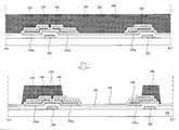
도 3은 본 발명의 제 1 실시예에 따른 COT구조 액정표시장치용 어레이기판의 일부를 개략적으로 도시한 평면도이고,3 is a plan view schematically illustrating a part of an array substrate for a COT structure liquid crystal display device according to a first embodiment of the present invention;
도 4a 내지 도 4g는 도 3의 Ⅳ-Ⅳ`를 따라 절단하여, 본 발명의 제 1 실시예에 따른 공정 순서에 따라 도시한 공정 단면도이고,4A to 4G are cross-sectional views illustrating a process sequence according to a first embodiment of the present invention, cut along line IV-IV ′ of FIG. 3;
도 5는 본 발명의 제 2 실시예에 따른 COT구조 액정표시장치용 어레이기판의 일부를 개략적으로 도시한 평면도이고,5 is a plan view schematically illustrating a portion of an array substrate for a COT structure liquid crystal display device according to a second embodiment of the present invention;
도 6a 내지 도 6k는 도 5의 Ⅵ-Ⅵ`을 따라 절단하여 본 발명의 제 2 실시예에 따른 공정 순서에 따라 도시한 공정 단면도이다.
6A through 6K are cross-sectional views illustrating a process sequence according to a second embodiment of the present invention cut along the line VI-VI ′ of FIG. 5.
<도면의 주요부분에 대한 간단한 설명><Brief description of the main parts of the drawing>
100 : 기판 102 : 게이트 배선100: substrate 102: gate wiring
104 : 게이트 전극 108 : 게이트 절연막104: gate electrode 108: gate insulating film
110 : 액티브층 112 : 오믹 콘택층110: active layer 112: ohmic contact layer
114 : 소스 전극 116 : 드레인 전극114: source electrode 116: drain electrode
120 : 제 1 보호막 124 : 블랙 매트릭스120: first protective film 124: black matrix
126 : 제 2 보호막 128 : 제 1 화소전극126: second protective film 128: first pixel electrode
130a,b : 컬러필터130a, b: Color filter
136 : 제 1 화소전극
136: first pixel electrode
본 발명은 액정표시장치에 관한 것으로, 박막트랜지스터 어레이부의 상부에 컬러필터를 구성하는 COT(color filter on TFT)구조 액정표시장치와 그 제조방법에 관한 것이다.BACKGROUND OF THE
일반적으로, 액정표시장치는 액정분자의 광학적 이방성과 복굴절 특성을 이용하여 화상을 표현하는 것으로, 전계가 인가되면 액정의 배열이 달라지고 달라진 액정의 배열 방향에 따라 빛이 투과되는 특성 또한 달라진다.In general, a liquid crystal display device displays an image by using optical anisotropy and birefringence characteristics of liquid crystal molecules. When an electric field is applied, the alignment of liquid crystals is changed, and the characteristics of light transmission vary according to the arrangement direction of the changed liquid crystals.
일반적으로, 액정표시장치는 전계 생성 전극이 각각 형성되어 있는 두 기판을 두 전극이 형성되어 있는 면이 마주 대하도록 배치하고 두 기판 사이에 액정 물질을 주입한 다음, 두 전극에 전압을 인가하여 생성되는 전기장에 의해 액정 분자를 움직이게 함으로써, 이에 따라 달라지는 빛의 투과율에 의해 화상을 표현하는 장치이다.In general, a liquid crystal display device is formed by arranging two substrates on which electric field generating electrodes are formed so that the surfaces on which the two electrodes are formed face each other, injecting a liquid crystal material between the two substrates, and then applying a voltage to the two electrodes. By moving the liquid crystal molecules by the electric field is a device that represents the image by the transmittance of light that varies accordingly.
도 1은 일반적인 액정표시장치를 개략적으로 나타낸 도면이다.1 is a view schematically showing a general liquid crystal display device.
도시한 바와 같이, 일반적인 컬러 액정표시장치(11)는 서브 컬러필터(8)와 각 서브 컬러필터(8)사이에 구성된 블랙 매트릭스(6)를 포함하는 컬러필터(7)와 상기 컬러필터(7)의 상부에 증착된 공통전극(18)이 형성된 상부기판(5)과, 화소영역(P)이 정의되고 화소영역에는 화소전극(17)과 스위칭소자(T)가 구성되며, 화소영역(P)의 주변으로 어레이배선이 형성된 하부기판(22)과, 상부기판(5)과 하부기판(22) 사이에는 액정(14)이 충진되어 있다.As shown, a general color
상기 하부기판(22)은 어레이기판(array substrate)이라고도 하며, 스위칭 소자인 박막트랜지스터(T)가 매트릭스형태(matrix type)로 위치하고, 이러한 다수의 박막트랜지스터(TFT)를 교차하여 지나가는 게이트배선(13)과 데이터배선(15)이 형성된다.The
이때, 상기 화소영역(P)은 상기 게이트배선(13)과 데이터배선(15)이 교차하여 정의되는 영역이며, 상기 화소영역(P)상에는 전술한 바와 같이 투명한 화소전극(17)이 형성된다.In this case, the pixel area P is an area defined by the
상기 화소전극(17)은 인듐-틴-옥사이드(indium-tin-oxide : ITO)와 같이 빛의 투과율이 비교적 뛰어난 투명 도전성금속을 사용한다.The
상기 화소전극(17)과 병렬로 연결된 스토리지 캐패시터(C)가 게이트 배선(13)의 상부에 구성되며, 스토리지 캐패시터(C)의 제 1 전극으로 게이트 배선(13)의 일부를 사용하고, 제 2 전극으로 소스 및 드레인 전극과 동일층 동일물 질로 형성된 섬형상의 금속층(30)을 사용한다.A storage capacitor C connected in parallel with the
이때, 상기 섬형상의 금속층(30)은 화소전극(17)과 접촉되어 화소전극의 신호를 받도록 구성된다.In this case, the island-
전술한 바와 같이 상부 컬러필터 기판(5)과 하부 어레이기판(22)을 합착하여액정패널을 제작하는 경우에는, 컬러필터 기판(5)과 어레이기판(22)의 합착 오차에 의한 빛샘 불량 등이 발생할 확률이 매우 높다.As described above, when the upper
이하, 도 2를 참조하여 설명한다.A description with reference to FIG. 2 is as follows.
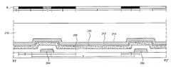
도 2는 도 1의 Ⅱ-Ⅱ`를 따라 절단한 단면도이다.FIG. 2 is a cross-sectional view taken along line II-II ′ of FIG. 1.
앞서 설명한 바와 같이, 어레이기판인 제 1 기판(22)과 컬러필터 기판인 제 2 기판(5)이 이격되어 구성되고, 제 1 및 제 2 기판(22,5)의 사이에는 액정층(14)이 위치한다.As described above, the
어레이기판(22)의 상부에는 게이트 전극(32)과 액티브층(34)과 소스 전극(36)과 드레인 전극(38)을 포함하는 박막트랜지스터(T)와, 상기 박막트랜지스터(T)의 상부에는 이를 보호하는 보호막(40)이 구성된다.The thin film transistor T including the
화소영역(P)에는 상기 박막트랜지스터(T)의 드레인 전극(38)과 접촉하는 투명 화소전극(17)이 구성되고, 화소전극(17)과 병렬로 연결된 스토리지 캐패시터(C)가 게이트 배선(13)의 상부에 구성된다.In the pixel region P, a
상기 상부 기판(5)에는 상기 게이트 배선(13)과 데이터 배선(15)과 박막트랜지스터(T)에 대응하여 블랙매트릭스(6)가 구성되고, 하부 기판(22)의 화소영역(P)에 대응하여 컬러필터(7a,7b,7c)가 구성된다.The
이때, 일반적인 어레이기판의 구성은 수직 크로스토크(cross talk)를 방지하기 위해 데이터 배선(15)과 화소 전극(17)을 일정 간격(A) 이격 하여 구성하게 되고, 게이트 배선(13)과 화소 전극 또한 일정간격(B) 이격 하여 구성하게 된다.In this case, the general array substrate is configured such that the
데이터 배선(15) 및 게이트 배선(13)과 화소 전극(17) 사이의 이격된 공간(A,B)은 빛샘 현상이 발생하는 영역이기 때문에, 상부 컬러필터기판(5)에 구성한 블랙 매트릭스(black matrix)(6)가 이 부분을 가려주는 역할을 하게 된다.Since the spaces A and B spaced apart between the
또한, 상기 박막트랜지스터(T)의 상부에 구성된 블랙매트릭스(6)는 외부에서 조사된 빛이 보호막(40)을 지나 액티브층(34)에 영향을 주지 않도록 하기 위해 빛을 차단하는 역할을 하게 된다.In addition, the
그런데, 상기 상부 기판(5)과 하부 기판(22)을 합착하는 공정 중 합착 오차(misalign)가 발생하는 경우가 있는데, 이를 감안하여 상기 블랙매트릭스(6)를 설계할 때 일정한 값의 마진(margin)을 두고 설계하기 때문에 그 만큼 개구율이 저하된다.However, a misalignment may occur during the process of bonding the
또한, 마진을 넘어선 합착오차가 발생할 경우, 빛샘 영역(A,B)이 블랙매트릭스(6)에 모두 가려지지 않는 빛샘 불량이 발생하는 경우가 종종 있다.In addition, in the case where the bonding error beyond the margin occurs, there is often a case of light leakage defects in which the light leakage regions A and B are not covered by the
이러한 경우에는 상기 빛샘이 외부로 나타나기 때문에 화질을 저하하는 문제가 있다.
In this case, since the light leakage appears to the outside, there is a problem of degrading the image quality.
본 발명은 전술한 바와 같은 문제를 해결하기 위해 제안된 것으로, 본 발명 을 요약하면 컬러필터를 하부기판에 구성하고 컬러필터 사이 영역 즉, 박막트랜지스터와 게이트 배선 및 데이터배선의 상부에 블랙매트릭스를 구성한다.SUMMARY OF THE INVENTION The present invention has been proposed to solve the above-described problems. To summarize the present invention, a color filter is formed on a lower substrate, and a black matrix is formed on the area between the color filters, that is, the thin film transistor, the gate wiring, and the data wiring. do.
상기 화소영역에는 제 1 투명전극과 컬러필터와 제 2 투명전극 순으로 구성하되, 상기 제 1 투명 전극은 드레인 전극과 직접 접촉하는 구성이고, 상기 제 2 투명 전극은 상기 제 1 투명 전극과 접촉하도록 구성한다.The pixel region includes a first transparent electrode, a color filter, and a second transparent electrode, wherein the first transparent electrode is in direct contact with the drain electrode, and the second transparent electrode is in contact with the first transparent electrode. Configure.
이때, 상기 제 2 투명 전극을 패턴하는 공정은 별도의 PR패턴공정을 진행하지 않고, 상기 제 2 투명 전극을 증착한 후, 화소영역에 대응하는 부분에만 레이저를 조사하여 결정화 한 후, 비정질의 전극만을 식각하는 식각용액을 사용하여 이를 제거하는 공정을 진행함으로서 제 2 투명 전극을 각 화소마다 독립적으로 패턴할 수 있게 된다. 이때,상기 레이저 뿐 아니라 UV 램프를 강하게 쬐어 결정화를 이룰 수 있다.In this case, the patterning of the second transparent electrode is performed without depositing a separate PR pattern process, and after depositing the second transparent electrode, crystallizing by irradiating only a portion corresponding to the pixel region with an amorphous electrode. The second transparent electrode may be independently patterned for each pixel by performing a process of removing the same using an etching solution for etching only the bay. In this case, crystallization may be achieved by intensely irradiating not only the laser but also a UV lamp.
이와 같이 하면, 별도의 PR패턴 공정을 진행하지 않아도 되므로 PR 패턴 시 필요한 현상액이나 제거액(stripper)에 의해 하부의 컬러필터 패턴이 데미지를 입지 않게 된다.In this case, since a separate PR pattern process does not need to be performed, the lower color filter pattern is not damaged by the developer or stripper required for the PR pattern.
따라서, 고화질의 액정표시장치를 제작할 수 있다.
Therefore, a high quality liquid crystal display device can be manufactured.
전술한 목적을 달성하기 위한 본 발명에 따른 액정표시장치용 어레이기판은 기판 상에 구성되고, 일 방향으로 연장된 게이트 배선을 형성하는 단계와; 상기 게이트 배선과 제 1 절연막을 사이에 두고 수직하게 교차하여 다수의 화소영역을 정 의하는 데이터 배선을 형성하는 단계와; 상기 게이트 배선과 데이터 배선의 교차지점에 위치하고, 게이트 전극과 액티브층과 소스 전극과 드레인 전극을 포함하는 박막트랜지스터를 형성하는 단계와; 상기 드레인 전극의 일부를 제외한 박막트랜지스터의 상부와, 게이트 배선 및 데이터 배선의 상부 블랙매트릭스를 형성하는 단계와; 상기 블랙매트릭스가 형성된 기판의 전면에 제 2 절연막을 증착한 후, 제 2절연막과 하부의 제 1 절연막을 식각하여, 상기 드레인 전극의 일부를 노출하고 상기 화소영역에 대응하는 기판의 표면을 노출하는 단계와; 상기 패턴된 제 2 절연막이 형성된 기판에 투명 도전성 물질을 증착하고 패턴하여, 상기 노출된 드레인 전극과 접촉하면서 상기 화소영역에 투명 제 1 화소전극을 형성하는 단계와; 상기 제 1 화소전극의 상부에 컬러필터를 형성하는 단계와; 상기 컬러필터가 형성된 기판의 전면에 투명 도전성 물질을 증착하고, 상기 컬러필터 패턴에 대응한 부분에만 레이저를 조사하여 결정화하는 단계와; 상기 결정화 되지 않은 부분의 비정질 투명전극을 제거하여, 상기 화소영역에 대응하여 하부의 제 1 화소전극과 접촉하는 결정화된 제 2 화소전극을 형성하는 단계를 포함한다.An array substrate for a liquid crystal display device according to the present invention for achieving the above object is formed on a substrate, forming a gate wiring extending in one direction; Forming a data line defining a plurality of pixel regions by crossing the gate line and the first insulating layer in a vertical direction; Forming a thin film transistor positioned at an intersection point of the gate line and the data line, the thin film transistor including a gate electrode, an active layer, a source electrode, and a drain electrode; Forming an upper portion of the thin film transistor except for a portion of the drain electrode and an upper black matrix of the gate line and the data line; After depositing a second insulating film on the entire surface of the substrate on which the black matrix is formed, the second insulating film and the lower first insulating film are etched to expose a part of the drain electrode and to expose a surface of the substrate corresponding to the pixel region. Steps; Depositing and patterning a transparent conductive material on a substrate on which the patterned second insulating film is formed, thereby forming a transparent first pixel electrode in the pixel region while contacting the exposed drain electrode; Forming a color filter on the first pixel electrode; Depositing a transparent conductive material on the entire surface of the substrate on which the color filter is formed, and crystallizing by irradiating a laser only on a portion corresponding to the color filter pattern; And removing the amorphous transparent electrode of the non-crystallized portion to form a crystallized second pixel electrode in contact with the lower first pixel electrode corresponding to the pixel region.
상기 반도체층은 순수 비정질 실리콘으로 형성된 액티브층과, 불순물 비정질 실리콘으로 형성된 오믹 콘택층이다.The semiconductor layer is an active layer formed of pure amorphous silicon and an ohmic contact layer formed of impurity amorphous silicon.
상기 게이트 배선의 상부에 상기 제 1 및 제 2 화소전극과 접촉하는 아일랜드 형상의 금속층을 더욱 형성하여 이를 제 1 전극으로 하고, 그 하부의 게이트 배선을 제 2 전극으로 하는 보조 용량부를 형성하는 단계를 더욱 포함한다.And forming an island-shaped metal layer in contact with the first and second pixel electrodes on the upper portion of the gate wiring to form a first electrode, and forming an auxiliary capacitor having the lower gate wiring as a second electrode. It includes more.
상기 박막트랜지스터와 블랙매트릭스 사이에 무기 절연층을 형성하는 단계를 더욱 포함한다.The method may further include forming an inorganic insulating layer between the thin film transistor and the black matrix.
상기 무기절연층을 형성하는 물질은 질화 실리콘(SiNx) 또는 산화 실리콘(SiO2)이다.The material forming the inorganic insulating layer is silicon nitride (SiNx ) or silicon oxide (SiO2 ).
상기 컬러필터 패턴은 상기 화소영역에 적색과 녹색과 청색의 컬러필터 패턴이 각각 대응되도록 형성되며, 상기 결정화되지 않은 비정질 투명전극 부분만을 제거하는 제거액은 OZ산(((COOH)2·H2O+H2O))이다.The color filter pattern is formed such that the color filter patterns of red, green, and blue correspond to the pixel area, respectively, and the removal liquid for removing only the non-crystallized amorphous transparent electrode portion is OZ acid (((COOH)2 · H2 O). + H2 O)).
본 발명의 특징에 따른 액정표시장치용 어레이기판 제조방법은 기판 상에 일 방향으로 연장된 게이트 배선과, 이에 연결된 게이트 전극을 형성하는 단계와; 상기 게이트 전극 상부에 제 1 절연막을 사이에 두고 적층된 액티브 층과 오믹콘택층과, 오믹 콘택층과 접촉하고 소정간격 이격된 소스 전극과 드레인 전극과, 소스 전극에서 연장된 데이터 배선을 동시에 형성하는 단계와; 상기 소스 및 드레인 전극과 데이터 배선의 상부에 블랙매트릭스를 형성하는 단계와; 상기 블랙매트릭스가 형성된 기판의 전면에 제 2 절연막을 증착한 후, 제 2절연막과 하부의 제 1 절연막을 식각하여, 상기 드레인 전극의 일부를 노출하고 상기 화소영역에 대응하는 기판의 표면을 노출하는 단계와; 상기 패턴된 제 2 절연막이 형성된 기판에 투명 도전성 물질을 증착하고 패턴하여, 상기 노출된 드레인 전극과 접촉하면서 상기 화소영역에 투명 제 1 화소전극을 형성하는 단계와; 상기 화소영역의 제 1 전극 상부에 컬러필터를 형성하는 단계와; 상기 컬러필터가 형성된 기판의 전면에 투명 도전성 물질을 증착하고, 상기 컬러필터에 대응한 부분에만 레이저를 조사하여 결정화하는 단계와; 상기 결정화 되지 않은 부분의 비정질 투명전극을 제거하여, 상기 화소영역에 대응하여 하부의 제 1 화소전극과 접촉하는 결정화된 제 2 화소전극을 형성하는 단계를 포함한다.According to an aspect of the present invention, there is provided a method of manufacturing an array substrate for a liquid crystal display device, the method including: forming a gate wiring extending in one direction and a gate electrode connected thereto; Simultaneously forming an active layer and an ohmic contact layer stacked on the gate electrode with the first insulating layer interposed therebetween, a source electrode and a drain electrode contacting the ohmic contact layer and spaced a predetermined distance from each other, and a data line extending from the source electrode. Steps; Forming a black matrix on the source and drain electrodes and the data line; After depositing a second insulating film on the entire surface of the substrate on which the black matrix is formed, the second insulating film and the lower first insulating film are etched to expose a part of the drain electrode and to expose a surface of the substrate corresponding to the pixel region. Steps; Depositing and patterning a transparent conductive material on a substrate on which the patterned second insulating film is formed, thereby forming a transparent first pixel electrode in the pixel region while contacting the exposed drain electrode; Forming a color filter on the first electrode of the pixel region; Depositing a transparent conductive material on the entire surface of the substrate on which the color filter is formed, and crystallizing the laser by irradiating only a portion corresponding to the color filter; And removing the amorphous transparent electrode of the non-crystallized portion to form a crystallized second pixel electrode in contact with the lower first pixel electrode corresponding to the pixel region.
상기 블랙매트릭스는 불투명한 감광성 유기 물질로 형성한다.The black matrix is formed of an opaque photosensitive organic material.
상기 게이트 배선의 상부에 상기 제 1 및 제 2 화소전극과 접촉하는 아일랜드 형상의 금속층을 더욱 형성하여 이를 제 1 전극으로 하고, 그 하부의 게이트 배선을 제 2 전극으로 하는 보조 용량부를 형성하는 단계를 더욱 포함한다.And forming an island-shaped metal layer in contact with the first and second pixel electrodes on the upper portion of the gate wiring to form a first electrode, and forming an auxiliary capacitor having the lower gate wiring as a second electrode. It includes more.
상기 결정화되지 않은 비정질 투명전극 부분만을 제거하는 제거액은 OZ산((COOH)2·H2O+H2O))이다.The removal liquid for removing only the non-crystallized amorphous transparent electrode portion is OZ acid ((COOH)2 .H2 O + H2 O).
전술한 바와 같은 공정에서, 상기 액티브층과 소스 및 드레인 전극과 데이터 배선을 동시에 형성하는 단계는, 상기 게이트 배선과 게이트 전극이 형성된 기판의 전면에 제 1 절연막과 순수 비정질 실리콘층과 불순물 비정질 실리콘층과 오믹 콘택층과 금속층을 적층하는 단계와; 상기 금속층 상부에 포토레지스트층을 형성하고, 포토 레지스트층과 이격된 상부에 투과부의 차단부와 반투과부로 구성된 마스크를 위치시키는 단계와; 상기 마스크의 상부에 빛을 조사하여 하부의 포토레지스트층을 노광하고 현상하여, 상기 게이트 전극 상부에 서로 다른 높이로 패턴된 제 1 포토패턴과, 상기 게이트 배선과는 수직한 형상으로 제 2 포토패턴을 형성하는 단계와; 상기 제 1 및 제 2 포토패턴 사이로 노출된 금속층과 하부의 불순물 비정질 실리콘층과 그 하부의 순수 비정질 실리콘층을 제거하여, 데이터 배선과 이에 연장된 소스-드레인 전극층과, 소스-드레인 전극층의 하부에 제 1 반도체층과 제 1 반도체층에서 상기 데이터 배선의 하부로 연장된 제 2 반도체층을 형성하는 단계와; 상기 제 1 및 제 2 포토 패턴을 애싱하는 공정을 진행하여, 상기 소스-드레인 전극층의 중앙부를 노출하는 단계와; 상기 노출된 소스 드레인 전극층을 식각하여 이격된 소스 전극과 드레인 전극을 형성하는 단계를 더욱 포함한다.In the process as described above, the step of simultaneously forming the active layer, the source and drain electrodes and the data wiring, the first insulating film, the pure amorphous silicon layer and the impurity amorphous silicon layer on the entire surface of the substrate on which the gate wiring and the gate electrode is formed Stacking the ohmic contact layer and the metal layer; Forming a photoresist layer on the metal layer, and placing a mask including a blocking portion and a semi-transmissive portion on a portion spaced apart from the photoresist layer; Exposing and developing a lower photoresist layer by irradiating light on the upper portion of the mask to form a first photo pattern patterned at different heights on the gate electrode and a second photo pattern perpendicular to the gate wiring; Forming a; The metal layer exposed between the first and second photo patterns, the lower impurity amorphous silicon layer and the lower pure amorphous silicon layer are removed to remove the data line, the source-drain electrode layer and the source-drain electrode layer extending therefrom. Forming a second semiconductor layer extending below the data line in the first semiconductor layer and the first semiconductor layer; Performing a process of ashing the first and second photo patterns to expose a central portion of the source-drain electrode layer; Etching the exposed source drain electrode layer to form a spaced source electrode and a drain electrode.
상기 제 1 반도체층과 제 2 반도체층은 패턴된 비정질 실리콘층과 불순물 비정질 실리콘층이 적층되어 구성된되며, 상기 소스 및 드레인 전극층을 형성하는 공정에서, 상기 제 1 반도체층의 불순물 비정질 실리콘층이 제거된다.The first semiconductor layer and the second semiconductor layer are formed by stacking a patterned amorphous silicon layer and an impurity amorphous silicon layer, and in the process of forming the source and drain electrode layers, the impurity amorphous silicon layer of the first semiconductor layer is removed. do.
상기 데이터 배선과 소스 및 드레인 전극의 주변으로 하부의 비정질 실리콘층이 노출되어 형성된다.A lower portion of the amorphous silicon layer is formed around the data line and the source and drain electrodes.
이하 첨부한 도면을 참조하여, 본 발명에 따른 바람직한 실시예들을 설명한다.
Hereinafter, exemplary embodiments of the present invention will be described with reference to the accompanying drawings.
-- 제 1 실시예 --First Embodiment
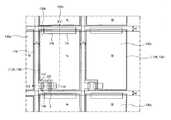
도 3은 본 발명에 따른 액정표시장치용 어레이기판의 구성을 개략적으로 도시한 도면이다.3 is a view schematically showing a configuration of an array substrate for a liquid crystal display device according to the present invention.
도시한 바와 같이, 기판(100)상에 일 방향으로 연장된 게이트 배선(102)을 서로 평행하게 구성하고, 상기 게이트 배선(102)과 수직하게 교차하여 다수의 화소영역(P)을 정의하는 데이터 배선(116)을 구성한다.As shown in the drawing, the data forming the
상기 게이트 배선(102)과 데이터 배선(116)이 교차하는 지점에는 게이트 전 극(104)과 액티브층(108)과 소스 및 드레인 전극(112,114)을 포함하는 박막트랜지스터(T)를 구성한다.The thin film transistor T including the
상기 두 배선(102,116)이 교차하여 정의되는 영역(P)에는 드레인 전극(114)과 접촉하는 이중층의 투명 화소전극(128,136)과 컬러필터(130a,130b,130c)를 구성한다.In the region P defined by the crossing of the two
상기 투명 전극(128,136)은 이중 층으로 구성되며, 이중 제 1 전극(128)은 드레인 전극(114)과 접촉하면서 컬러필터(130a,130b,130c)의 하부에 구성하고, 제 2 전극(136)은 컬러필터(130a,130b,130c)의 상부에 구성한다.The
상기 제 2 전극(136)은 제 1 전극(128)을 통해 드레인 전극(114)과 간접적으로 접촉하는 형상이다.The
제 1 및 제 2 투명 전극(128,136)은 게이트배선(102)의 상부에 구성된 스토리지 캐패시터(Cst)와 병렬로 연결된다.The first and second
스토리지 캐패시터(Cst)는 게이트 배선(102)의 일부를 제 1 전극으로 하고, 상기 제 1 및 제 2 투명전극(제 1 및 제 2 화소전극)(128,136)과 연결되는 동시에 상기 소스 및 드레인 전극과 동일층 동일물질로 형성된 섬형상의 금속층(118)을 제 2 전극으로 한다.The storage capacitor Cst has a portion of the
COT구조는 도시한 바와 같이, 상기 박막트랜지스터(T) 어레이부의 상부에 블랙매트릭스(124)와, 적, 녹, 청색의 컬러필터(130a,130b,130c)가 구성된 형태이다.As illustrated, the COT structure includes a
블랙매트릭스(124)는 빛샘영역을 가리는 역할을 하며, 게이트 배선 및 데이 터 배선(116)과 박막트랜지스터(T)에 대응하여 구성한다.The
상기 블랙매트릭스(124)는 불투명한 유기물질을 도포하여 형성하며, 빛을 차단하는 역할과 함께 박막트랜지스터를 보호하는 보호막의 역할을 하게 된다.The
전술한 구성에서, 상기 컬러필터의 상부에 제 2 투명전극(제 2 화소전극)을 형성할 때 별도의 포토공정을 사용하지 않기 때문에 하부의 컬러필터 패턴이 데미지를 입는 불량을 방지할 수 있다.In the above-described configuration, since a separate photo process is not used when the second transparent electrode (second pixel electrode) is formed on the color filter, a defect in which the lower color filter pattern is damaged may be prevented.
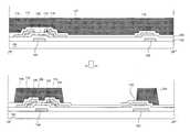
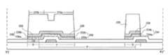
이하, 도 4a 내지 도 4g를 참조하여, 본 발명의 실시예에 따른 액정표시장치용 어레이기판의 제조방법을 설명한다.Hereinafter, a method of manufacturing an array substrate for a liquid crystal display device according to an exemplary embodiment of the present invention will be described with reference to FIGS. 4A to 4G.
도 4a 내지 도 4g는 도 3의 Ⅳ-Ⅳ`를 절단하여, 본 발명의 제 1 실시예에 따른 공정 순서로 도시한 공정 단면도이다.4A to 4G are cross-sectional views illustrating the process sequence according to the first embodiment of the present invention, taken along the line IV-IV ′ of FIG. 3.
(도 3의 절단선 Ⅳ-Ⅳ`는 박막트랜지스터와 화소의 절단선이다.)(Cutting lines IV-IV` in FIG. 3 are cutting lines between the thin film transistor and the pixel.)
도 4a에 도시한 바와 같이, 기판(100)상에 도전성 금속을 증착하고 제 1 마스크 공정으로 패턴하여, 게이트 배선(102)과 게이트 전극(104)을 형성한다.As shown in FIG. 4A, a conductive metal is deposited on the
상기 게이트 배선(104)과 게이트 전극(102)이 형성된 기판(100)의 전면에 질화 실리콘(SiNX)과 산화 실리콘(SiO2)을 포함하는 무기절연물질 그룹 중 선택된 하나를 증착하여 제 1 절연층인 게이트 절연막(106)을 형성한다.First insulation is deposited by depositing one selected from the group of inorganic insulating materials including silicon nitride (SiNX ) and silicon oxide (SiO2 ) on the entire surface of the
상기 게이트 절연막(106)상에 순수 비정질 실리콘(a-Si:H)과 불순물이 포함된 비정질 실리콘(n+a-Si:H)을 증착하고 제 2 마스크 공정으로 패턴하여, 게이트 전극(104)상부의 게이트 절연막(106)상에 액티브층(108)과 오믹 콘택층(110)을 형 성한다.Pure amorphous silicon (a-Si: H) and amorphous silicon (n + a-Si: H) containing impurities are deposited on the
다음으로 도4b에 도시한 바와 같이, 상기 액티브층(108)과 오믹 콘택층(110)이 형성된 기판(100)의 전면에 크롬(Cr) 또는 몰리브덴(Mo)을 증착하고 제 3 마스크 공정으로 패턴하여, 상기 오믹 콘택층(110)과 각각 접촉하는 소스 전극(112)과 드레인 전극(114)과, 상기 소스전극(112)과 연결된 데이터배선(116)과, 상기 게이트 배선(102)의 상부에 아일랜드 형상의 소스/ 드레인 금속층(118)을 형성한다.Next, as shown in FIG. 4B, chromium (Cr) or molybdenum (Mo) is deposited on the entire surface of the
상기 소스 및 드레인 전극(112,114)이 형성된 기판(100)의 전면에 질화 실리콘(SiN2)과 산화 실리콘(SiO2)을 포함한 무기절연물질 그룹 중 선택된 하나를 증측하여 제 2 절연막(120)을 형성한다.The second
이때, 제 2 절연막(120)의 기능은 이후에 형성되는 유기막(블랙매트릭스)과 상기 액티브층(108)사이에 발생할 수 있는 접촉불량을 방지하기 위한 기능을 한다.In this case, the function of the second insulating
제 2 절연막(120)은 상기 유기막과 액티브층(108)사이에 접촉불량이 발생하지 않는다면 굳이 형성하지 않아도 좋다.The second
전술한 바와 같은 공정을 통해 박막트랜지스터 어레이부를 형성하는 공정이 완료된다.The process of forming the thin film transistor array unit through the above-described process is completed.
다음으로, 도 4c에 도시한 바와 같이, 상기 제 2 절연막(120)상부에 유전율이 낮은 불투명한 유기물질을 도포하여 블랙 유기층(122)을 형성하고 제 4 마스크 공정으로 패턴하여, 상기 박막트랜지스터(T)와 데이터 배선(116)및 게이트 배선(102)의 상부에 블랙매트릭스(124)를 형성한다.Next, as illustrated in FIG. 4C, an opaque organic material having a low dielectric constant is coated on the second insulating
다음으로, 도 4d에 도시한 바와 같이, 상기 블랙매트릭스(124)가 형성된 기판(100)의 전면에 절연물질을 증착하여 제 3 절연막(126)을 형성한다.Next, as shown in FIG. 4D, an insulating material is deposited on the entire surface of the
상기 제 3 절연막(126)은 질화 실리콘(SiNX)과 산화 실리콘(SiO2)을 포함하는 무기절연물질 그룹 중 선택된 하나를 증착하여 사용하거나, 경우에 따라서는 벤조사이클로부텐(BCB)과 아크릴(acryl)계 수지(resin)를 포함하는 유기절연물질 그룹 중 선택된 하나를 도포하여 사용한다.The third
도 4e에 도시한 바와 같이, 제 5 마스크 공정으로 상기 제 3 절연막(126)과 제 2 절연막(120)과 게이트 절연막(106)을 식각하여, 상기 드레인 전극(114)일 측과 화소영역(P)과, 상기 섬형상의 금속층(118)의 일측을 노출하는 공정을 진행한다.As shown in FIG. 4E, the third insulating
도 4f에 도시한 바와 같이, 상기 패턴된 제 3 절연막(126)이 형성된 기판(100)의 전면에 전술한 바와 같은 인듐-틴-옥사이드(ITO)와 인듐-징크-옥사이드(IZO)를 포함하는 투명한 도전성 금속을 증착하고 제 6 마스크 공정으로 패턴하여, 상기 노출된 드레인 전극(114)과 상기 소스/드레인 금속층(118)과 동시에 접촉하면서 화소영역(P)에 위치하는 제 1 화소전극(128)을 형성한다.As shown in FIG. 4F, indium tin oxide (ITO) and indium zinc oxide (IZO) as described above are formed on the entire surface of the
연속하여, 상기 제 1 화소전극(128)이 형성된 기판(100)의 전면에 컬러수지를 도포하여, 다수의 화소영역(P)에 적색과 녹색과 청색의 컬러필터(130a,130b,도 3의 130c)를 각각 형성한다.Subsequently, color resins are applied to the entire surface of the
도 4g에 도시한 바와 같이, 상기 다수의 컬러필터 패턴(130a,130b,도 3의130c)이 형성된 기판(100)의 전면에 앞서 설명한 투명전극을 증착하여 투명전극층(132)을 증착한다.As shown in FIG. 4G, the transparent electrode is deposited on the entire surface of the
이때, 증착된 투명전극층(132)은 비정질 상태이며, KrF를 광원으로 하는 레이저를 조사하여 부분적으로 결정화를 진행한다.At this time, the deposited
즉, 화소영역(P)에 대응하는 부분에 집중적으로 레이저를 조사하여 결정화를 진행한다. 이때, 레이저 이외에오 UV LAMP를 강하게 쬐어 결정화 할 수도 있다.That is, crystallization is performed by intensively irradiating a laser to a portion corresponding to the pixel region P. FIG. At this time, in addition to the laser, UV LAMP may be strongly exposed to crystallize.
상기 부분적으로 결정화기 진행된 투명전극을 OZ산 즉, ((COOH)2·H2O+H2O)에 담그게 되면 상기 비정질 부분만 제거되어 상기 화소영역(P)에는 상기 제 1 화소전극(128)과 접촉하면서 상기 컬러필터 패턴(130a,130b,도 3의 130c) 상부에 구성되는 제 2 화소전극(136)을 형성할 수 있다.When the partially crystallized transparent electrode is immersed in OZ acid, that is, ((COOH)2 · H2 O + H2 O), only the amorphous portion is removed and the first pixel electrode (P) is disposed in the pixel region (P). The
이때, 상기 제 2 화소전극(136)을 형성하는 공정에서 별도의 포토공정을 진행하지 않기 때문에 포토 공정시 현상액에 의해 하부의 컬러필터 패턴이 데미지를 입는 것을 방지할 수 있다.In this case, since a separate photo process is not performed in the process of forming the
이상과 같은 공정을 통해 본 발명에 따른 COT구조의 액정표시장치용 기판을 제작할 수 있다.Through the above process, it is possible to manufacture a substrate for a liquid crystal display device having a COT structure according to the present invention.
전술한 바와 같은 공정은 상기 컬러필터를 형성하는 공정을 제외하고, 6마스크 공정으로 어레이 기판을 제작하였다.As described above, the array substrate was manufactured by the six mask process except for the process of forming the color filter.
이하, 제 2 실시예는 상기 제 1 실시예의 변형 예로서, 제 1 실시예에 비해 공정을 더욱 단순화 할 수 있는 방법을 제안한다.Hereinafter, the second embodiment proposes a modified example of the first embodiment, which can further simplify the process compared to the first embodiment.
-- 제 2 실시예 --Second Embodiment
본 발명의 제 2 실시예는 전술한 박막트랜지스터 어레이부의 공정에서 상기 소스 및 드레인 전극과 액티브층을 한꺼번에 패턴하여 COT 구조의 액정표시장치를 제작하는 방법을 제안한다.The second embodiment of the present invention proposes a method of manufacturing a liquid crystal display device having a COT structure by patterning the source and drain electrodes and the active layer at the same time in the above-described thin film transistor array unit process.
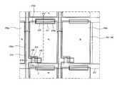
도 5는 본 발명의 제 2 실시예에 따른 COT구조의 액정표시장치용 하부기판의 구성을 개략적으로 도시한 평면도이다.5 is a plan view schematically illustrating a configuration of a lower substrate for a liquid crystal display device having a COT structure according to a second embodiment of the present invention.
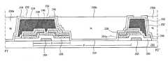
도시한 바와 같이, 기판(200)상에 일 방향으로 연장된 게이트 배선(202)을 서로 평행하게 구성하고, 상기 게이트 배선(202)과 수직하게 교차하여 다수의 화소영역(P)을 정의하는 데이터 배선(224)을 구성한다.As shown in the drawing, the data forming the
상기 게이트 배선(202)과 데이터 배선(224)이 교차하는 지점에는 게이트 전극(204)과 액티브층(232a)과 소스 및 드레인 전극(238,240)을 포함하는 박막트랜지스터(T)를 구성한다.The thin film transistor T including the
상기 두 배선(202,224)이 교차하여 정의되는 영역(P)에는 드레인 전극(240)과 접촉하는 투명전극(254,260)과 컬러필터(256a,256b,256c)를 구성한다.In the region P defined by the crossing of the two
상기 투명 전극(254,260)은 이중 층으로 구성되며, 이중 제 1 전극(254)은 드레인 전극(240)과 접촉하면서 컬러필터(256a,256b,256c)의 하부에 구성하고, 제 2 전극(260)은 컬러필터(256a,256b,256c)의 상부에 구성한다.The
상기 상기 제 2 전극(260)은 제 1 전극(254)을 통해 드레인 전극(240)과 간접적으로 접촉하는 형상이다.The
제 1 및 제 2 투명 전극(254,260)은 게이트배선(202)의 상부에 구성된 스토 리지 캐패시터(Cst)와 병렬로 연결된다.The first and second
스토리지 캐패시터(Cst)는 게이트 배선(202)의 일부를 제 1 전극으로 하고, 상기 제 1 및 제 2 투명전극(254,260)과 연결되는 동시에 상기 소스 및 드레인 전극(238,240)과 동일층 동일물질로 형성된 섬형상의 금속층(228)을 제 2 전극으로 한다.The storage capacitor Cst has a portion of the
이때, 상기 소스 및 드레인 전극(238,240)과 액티브층(232a)은 동일한 공정에서 동시에 형성되며, 이러한 경우에는 도시한 바와 같이, 필연적으로 상기 데이터 배선과 소스 및 드레인 전극(238,240)과 섬형상의 금속층(228)의 주변으로 비정질 실리콘층(230a, 232a, 234a)이 노출되는 형상이 된다.In this case, the source and drain
COT구조는 도시한 바와 같이, 상기 박막트랜지스터(T) 어레이부의 상부에 블랙매트릭스(250)와, 적, 녹, 청색의 컬러필터(256a,256b,256c)가 구성된 형태이다.As illustrated, the COT structure includes a
블랙매트릭스(250)는 빛샘영역을 가리는 역할을 하며, 게이트 배선 및 데이터 배선(224)과 박막트랜지스터(T)에 대응하여 구성한다.The
상기 블랙매트릭스(254)는 불투명한 유기물질을 도포하여 형성하며, 빛을 차단하는 역할과 함께 박막트랜지스터를 보호하는 보호막의 역할을 하게 된다.The
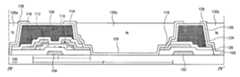
이하, 도 6a 내지 도 6k를 참조하여, 본 발명의 제 2 실시예에 따른 COT구조의 박막트랜지스터 어레이부와 컬러필터부의 제조공정을 설명한다.6A to 6K, the manufacturing process of the thin film transistor array unit and the color filter unit of the COT structure according to the second embodiment of the present invention will be described.
도 6a 내지 도 6k는 도 5의 Ⅵ-Ⅵ`을 따라 절단하여, 본 발명의 제 2 실시예에 따른 공정순서로 도시한 공정 단면도이다.6A to 6K are cross-sectional views illustrating a process sequence according to a second embodiment of the present invention, cut along VI-VI ′ of FIG. 5.
도 6a에 도시한 바와 같이, 기판(200)상에 박막트랜지스터 영역(T)과 화소영역(P)과 데이터 영역(D)과 스토리지 영역(S)을 정의한다.As shown in FIG. 6A, a thin film transistor region T, a pixel region P, a data region D, and a storage region S are defined on the
상기 다수의 영역(D,T,P,S)이 정의된 기판(200)의 전면에 도전성 금속을 증착하고 제 1 마스크 공정으로 패턴하여, 게이트 배선(202)과 게이트 전극(204)을 형성한다.A conductive metal is deposited on the entire surface of the
다음으로, 도 6b에 도시한 바와 같이, 상기 게이트 배선(204)과 게이트 전극(202)이 형성된 기판(200)의 전면에 질화 실리콘(SiNX)과 산화 실리콘(SiO2)을 포함하는 무기절연물질 그룹 중 선택된 하나를 증착하여 제 1 절연층인 게이트 절연막(208)을 형성한다.Next, as shown in FIG. 6B, an inorganic insulating layer including silicon nitride (SiNX ) and silicon oxide (SiO2 ) is formed on the entire surface of the
상기 게이트 절연막(208)상에 순수 비정질 실리콘(a-Si:H)층(210)과 불순물이 포함된 비정질 실리콘(n+a-Si:H)층(212)과 제 2 금속층(214)을 순차적으로 형성한다. 연속하여, 상기 제 2 금속층(214)의 상부에 포토레지스트를 도포하여 PR층(216)을 형성한다.A pure amorphous silicon (a-Si: H)
이때, 상기 제 2 금속층은 크롬(Cr), 몰리브덴(Mo), 구리(Cu), 텅스텐(W), 티타늄(Ti), 알루미늄(Al), 알루미늄합금(AlNd)을 포함하는 도전성 금속그룹 중 선택된 하나로 형성할 수 있다.In this case, the second metal layer is selected from a conductive metal group including chromium (Cr), molybdenum (Mo), copper (Cu), tungsten (W), titanium (Ti), aluminum (Al), and aluminum alloy (AlNd). Can be formed into one.
연속하여, 상기 기판(200)과 이격된 상부에 투과부(A)와 차단부(B)와 반투과부(C)로 구성된 마스크(M)를 위치시킨다.Subsequently, a mask M including a transmissive part A, a blocking part B, and a transflective part C is positioned on an upper portion separated from the
이때, 상기 차단부(B)는 데이터 영역(D)과 박막트랜지스터 영역(T)과 스토리 지 영역(S)에 대응하고, 상기 반투과부(C)는 상기 박막트랜지스터 영역(T)의 일부에 대응하고, 상기 투과(C)부는 상기 박막트랜지스터 영역(T)을 제외한 화소영역(P)에 대응하도록 구성한다.In this case, the blocking part B corresponds to the data area D, the thin film transistor area T, and the storage area S, and the transflective part C corresponds to a part of the thin film transistor area T. The transmissive portion C is configured to correspond to the pixel region P except the thin film transistor region T. FIG.
상기 마스크의 상부로 빛을 조사하여 하부의 PR층을 노광하고 현상하게 되면, 도 6c에 도시한 바와 같이, 상기 박막트랜지스터 영역(T)에 대응하여 높이가 다른 PR패턴(220a)이 남게 되고, 상기 데이터 영역(D)과 스토리지 영역(S)에는 원래 도포된 높이 그대로의 PR패턴(220b)이 남게 된다.When the light is irradiated to the upper part of the mask to expose the lower PR layer and developed, as shown in FIG. 6C, a
상기 박막트랜지스터 영역(T)에 대응한 부분의 PR패턴(220a)의 높이가 서로 다른 이유는, 상기 마스크(도 6b의 M)의 반투과부(C)에 대응한 부분이 상부로부터 일부만 노광되고 현상되었기 때문이다.The reason why the height of the
연속하여, 상기 패턴된 PR층(220a,220b)사이로 노출된 하부의 제 2 금속층(214)과 불순물 비정질 실리콘층(212)과 순수 비정질 실리콘층(210)을 제거하는 공정을 진행하면, 도 6d에 도시한 바와 같이, 상기 패턴된 PR층(220a,220b)의 하부에 구성되고, 상기 데이터 영역(D)에 대응하여 데이터 배선(224)과, 상기 데이터 배선(224)과 연결되면서 상기 박막트랜지스터 영역(T)에 섬형상으로 구성된 소스-드레인 전극층(226)과, 상기 스토리지 영역(S)에 형성된 섬형상의 금속층(228)이 형성된다.Subsequently, the process of removing the lower
동시에, 상기 데이터 배선(224)의 하부에는 제 1 반도체 패턴(230)이 구성되고, 제 1 반도체 패턴(230)에서 상기 소스-드레인 전극층(226)의 하부로 연장된 제 2 반도체 패턴(232)이 구성되고, 상기 섬형상의 금속층(226)의 하부에는 제 3 반도 체 패턴(234)이 구성된다.At the same time, a
각각은 패턴된 순수 비정질 실리콘층(230a,232a,234a)과 불순물 비정질 실리콘층(230b,232b,234b)이 적층된 형상이다.Each of the patterns is formed by stacking the patterned pure
다음으로, 도 6e는 박막트랜지스터에 구성되는 액티브 채널층을 노출하기 위한 전단계인 PR패턴을 식각하는 애싱공정을 진행한 형상을 나타낸 도면이다.Next, FIG. 6E is a view illustrating an ashing process of etching a PR pattern, which is a previous step for exposing an active channel layer of a thin film transistor.
상기 마스크의 반투부(도 6b의 C)에 대응하여 일부만 노광된 부분은 이후 형성되는 액티브 채널에 대응하는 부분(E)이며, 일차로 이를 제거하기 위한 애싱공정(ashing processing)을 진행하게 된다. 상기 애싱공정은 일종의 건식식각 공정과 같으며, 상기 액티브 채널층에 대응하는 부분(E)의 PR패턴의 높이만큼 PR패턴이 전체적으로 제거된다.A portion partially exposed corresponding to the semi-permeable portion (C of FIG. 6B) of the mask is a portion E corresponding to an active channel to be formed later, and an ashing process is first performed to remove it. The ashing process is similar to a dry etching process, and the PR pattern is entirely removed by the height of the PR pattern of the portion E corresponding to the active channel layer.
상기 애싱공정을 통해 전체적으로 낮아진 PR패턴(236a,236b)의 주변(F)으로 상기 데이터 배선(224)과 소스-드레인 전극층(226)과, 섬형상의 금속층(228)이 노출되는 현상이 필연적으로 발생하게 된다.The phenomenon in which the
상기 PR패턴을 애싱하는 공정이 완료되면, 상기 액티브채널층(E)에 대응하여 노출된 소스-드레인 전극층(226)과 그 하부의 비정질 실리콘층(232b)을 제거하는 공정을 진행하고, 상기 남겨진 PR 패턴을 제거한다.When the process of ashing the PR pattern is completed, a process of removing the exposed source-
이때, 상기 PR패턴(236a,236b)의 주변(F)으로 노출된 금속층과 그 하부의 비정질 실리콘층(230b, 232b,234b) 또한 제거된다.In this case, the metal layer exposed to the periphery F of the
이와 같은 공정을 완료하면 결과적으로, 도 6f에 도시한 바와 같이, 상기 박막트랜지스터 영역(T)에 대응하여 서로 소정간격 이격되어 액티브 채널층(CH)을 노 출하는 소스 전극(238)과 드레인 전극(240)과, 소스 전극(238)에서 연장된 데이터 배선(224)과, 상기 게이트 배선(204)이 일부 상부에는 섬형상의 금속층(228)을 형성할 수 있다. 상기 각 구성요소의 주변으로는 필연적으로 순수 비정질 실리콘층(230a,232a,234a)이 노출된 형상이 된다.As a result, as shown in FIG. 6F, the
이때, 상기 박막트랜지스터 영역(T)에 대응하여 구성된 순수 비정질 실리콘층(232a)을 액티브층(active layer)이라 하고, 그 상부의 불순물 비정질 실리콘층(232b)을 오믹 콘택층(ohmic contact layer)이라 한다.In this case, the pure
이상과 같이, 도 6b와 도 6f를 통한 제 2 마스크 공정으로 박막트랜지스터 어레이부를 형성하는 공정이 완료되었다.As described above, the process of forming the thin film transistor array unit by the second mask process through FIGS. 6B and 6F is completed.
다음으로, 도 6g에 도시한 바와 같이, 상기 소스 및 드레이 전극(238,240)이 형성된 기판(200)의 전면에 질화 실리콘(SiN2)과 산화 실리콘(SiO2)을 포함한 무기절연물질 그룹 중 선택된 하나를 증착하여 제 2 절연막(246)을 형성한다.Next, as shown in FIG. 6G, one selected from the group of inorganic insulating materials including silicon nitride (SiN2 ) and silicon oxide (SiO2 ) on the entire surface of the
이때, 제 2 절연막(246)의 기능은 이후에 형성되는 유기막(미도시)과 상기 액티브층(232a)사이에 발생할 수 있는 접촉불량을 방지하기 위한 기능을 한다.In this case, the function of the second insulating
다음으로, 상기 제 2 절연막(246)상부에 유전율이 낮은 불투명한 유기물질을 도포하여 블랙 유기층(248)을 형성하고 제 3 마스크 공정으로 패턴하여, 상기 박막트랜지스터 영역(T)과 데이터 배선(224) 및 섬형상의 금속층(228)의 일부만을 가리도록 패턴된 블랙매트릭스(250)를 형성한다.Next, an opaque organic material having a low dielectric constant is coated on the second insulating
다음으로, 도 6h에 도시한 바와 같이, 상기 블랙매트릭스(250)가 형성된 기 판(200)의 전면에 절연물질을 증착하여 제 3 절연막(252)을 형성한다.Next, as shown in FIG. 6H, an insulating material is deposited on the entire surface of the
상기 제 3 절연막(252)은 질화 실리콘(SiNX)과 산화 실리콘(SiO2)을 포함하는 무기절연물질 그룹 중 선택된 하나를 증착하여 사용하거나, 경우에 따라서는 벤조사이클로부텐(BCB)과 아크릴(acryl)계 수지(resin)를 포함하는 유기절연물질 그룹 중 선택된 하나를 도포하여 사용한다 .The third
도 6i에 도시한 바와 같이, 제 4 마스크 공정으로 상기 제 3 절연막(252) 제 2 절연막(246)과 게이트 절연막(206)을 식각 하여, 상기 드레인 전극(240)의 일측과 화소영역(P)과, 상기 섬형상의 금속층(228)의 일측을 노출하는 공정을 진행한다.As illustrated in FIG. 6I, the third insulating
도 6j에 도시한 바와 같이, 상기 패턴된 제 3 절연막(252)이 형성된 기판(200)의 전면에 전술한 바와 같은 인듐-틴-옥사이드(ITO)와 인듐-징크-옥사이드(IZO)를 포함하는 투명한 도전성 금속을 증착하고 제 5 마스크 공정으로 패턴하여, 상기 노출된 드레인 전극(240)과 상기 섬형상의 금속층(228)과 동시에 접촉하면서 화소영역(P)에 위치하는 제 1 화소전극(254)을 형성한다.As shown in FIG. 6J, an indium tin oxide (ITO) and an indium zinc oxide (IZO) as described above are formed on the entire surface of the
연속하여, 상기 제 1 화소전극(254)이 형성된 기판(200)의 전면에 컬러수지를 도포하여, 다수의 화소영역(P)에 적색과 녹색과 청색의 컬러필터(256a,256b,도 5의 256c)를 각각 형성한다.Subsequently, color resins are applied to the entire surface of the
도 6k에 도시한 바와 같이, 상기 다수의 컬러필터 패턴(256a,256b,256c)이 형성된 기판(200)의 전면에 앞서 설명한 투명전극을 증착하여 투명전극층(258)을 증착한다.As illustrated in FIG. 6K, the transparent electrode is deposited on the entire surface of the
이때, 증착된 투명전극층(258)은 비정질 상태이며, KrF를 광원으로 하는 레이저를 조사하여 부분적으로 결정화를 진행한다.At this time, the deposited
즉, 화소영역(P)에 대응하는 부분에 집중적으로 레이저를 조사하여 결정화를 진행한다. 이때, 레이저 뿐 아니라 UV 램프를 강하게 쬐어 결정화 할 수 있다.That is, crystallization is performed by intensively irradiating a laser to a portion corresponding to the pixel region P. FIG. At this time, not only a laser but also a UV lamp may be strongly exposed to crystallize.
상기 부분적으로 결정화기 진행된 투명전극을 OZ산 즉, ((COOH)2·H2O+H2O)에 담그게 되면 상기 비정질 부분만 제거되어 상기 화소영역(P)에는 상기 제 1 화소전극(254)과 접촉하면서 상기 컬러필터 패턴(256a,256b,256c) 상부에 구성되는 제 2 화소전극(260)을 형성할 수 있다.When the partially crystallized transparent electrode is immersed in OZ acid, that is, ((COOH)2 · H2 O + H2 O), only the amorphous portion is removed and the first pixel electrode (P) is disposed in the pixel region (P). The
이때, 상기 제 2 화소전극(260)을 형성하는 공정에서 별도의 포토공정을 진행하지 않기 때문에 포토 공정 시 현상액에 의해 하부의 컬러필터 패턴이 데미지를 입는 것을 방지할 수 있다.In this case, since a separate photo process is not performed in the process of forming the
또한, 전술한 공정은 컬러필터 패턴 공정을 제외하고 상기 5 마스크 공정으로 제작되므로 상기 제 1 실시예에 비해 1마스크 공정을 줄여 공정시간을 단축하는 동시에 공정비용을 낮출 수 있는 장점이 있다.
In addition, since the above-described process is manufactured by the five mask process except for the color filter pattern process, there is an advantage that the process cost can be reduced while reducing the process time by reducing one mask process compared with the first embodiment.
본 발명에 따른 COT 구조의 액정표시장치는 어레이기판에 블랙매트릭스를 설계할 때 합착오차를 위한 공정마진을 둘 필요가 없으므로 개구율을 개선하는 효과 가 있다.The liquid crystal display of the COT structure according to the present invention has an effect of improving the aperture ratio since it is not necessary to place a process margin for bonding error when designing the black matrix on the array substrate.
또한, 제 2 화소전극을 형성하는 공정에서 사진식각 공정을 진행하지 않기 때문에 하부의 컬러필터가 상기 식각공정에서 사용되는 약액에 의해 데미지를 입지 않으므로 고화질을 구현하는 액정표시장치를 제작할 수 있는 효과가 있다.In addition, since the photolithography process is not performed in the process of forming the second pixel electrode, since the lower color filter is not damaged by the chemicals used in the etching process, it is possible to manufacture a liquid crystal display device that realizes high image quality. have.
또한, 박막트랜지스터를 형성할 때, 소스 및 드레인 전극과 액티브층을 1마스크 공정으로 형성함으로서, 공정시간 단축과 함께 공정비용을 낮추는 효과가 있다.
In addition, when forming the thin film transistor, by forming the source and drain electrodes and the active layer in one mask process, there is an effect of reducing the process time and the process cost.
Claims (20)
Translated fromKoreanPriority Applications (6)
| Application Number | Priority Date | Filing Date | Title |
|---|---|---|---|
| KR1020020078006AKR100916603B1 (en) | 2002-12-09 | 2002-12-09 | Manufacturing method of array substrate for liquid crystal display device |
| TW092129742ATWI227794B (en) | 2002-12-09 | 2003-10-27 | Manufacturing method of array substrate having color filter on thin film transistor structure |
| GB0325368AGB2396242B (en) | 2002-12-09 | 2003-10-30 | Manufacturing method of array substrate having colour filter on thin film transistor structure |
| CNB2003101154174ACN1267784C (en) | 2002-12-09 | 2003-11-25 | Method for producing array base plate with colour filter structure on thin film transistor for liquid crystal display device |
| JP2003395868AJP4299113B2 (en) | 2002-12-09 | 2003-11-26 | Method for manufacturing array substrate for liquid crystal display device |
| US10/736,620US7517620B2 (en) | 2002-12-09 | 2003-12-17 | Method for fabricating array substrate having color filter on thin film transistor structure for liquid crystal display device |
Applications Claiming Priority (1)
| Application Number | Priority Date | Filing Date | Title |
|---|---|---|---|
| KR1020020078006AKR100916603B1 (en) | 2002-12-09 | 2002-12-09 | Manufacturing method of array substrate for liquid crystal display device |
Publications (2)
| Publication Number | Publication Date |
|---|---|
| KR20040050235A KR20040050235A (en) | 2004-06-16 |
| KR100916603B1true KR100916603B1 (en) | 2009-09-14 |
Family
ID=29728805
Family Applications (1)
| Application Number | Title | Priority Date | Filing Date |
|---|---|---|---|
| KR1020020078006AExpired - Fee RelatedKR100916603B1 (en) | 2002-12-09 | 2002-12-09 | Manufacturing method of array substrate for liquid crystal display device |
Country Status (6)
| Country | Link |
|---|---|
| US (1) | US7517620B2 (en) |
| JP (1) | JP4299113B2 (en) |
| KR (1) | KR100916603B1 (en) |
| CN (1) | CN1267784C (en) |
| GB (1) | GB2396242B (en) |
| TW (1) | TWI227794B (en) |
Cited By (1)
| Publication number | Priority date | Publication date | Assignee | Title |
|---|---|---|---|---|
| KR101915223B1 (en)* | 2011-08-19 | 2019-01-15 | 엘지디스플레이 주식회사 | Array substrate for advanced high in plane switching mode liquid crystal display device and method for fabricating the same |
Families Citing this family (33)
| Publication number | Priority date | Publication date | Assignee | Title |
|---|---|---|---|---|
| KR100870700B1 (en)* | 2002-12-09 | 2008-11-27 | 엘지디스플레이 주식회사 | Array substrate for liquid crystal display device and manufacturing method |
| US7825021B2 (en)* | 2004-01-16 | 2010-11-02 | Semiconductor Energy Laboratory Co., Ltd. | Method for manufacturing display device |
| KR101100674B1 (en)* | 2004-06-30 | 2012-01-03 | 엘지디스플레이 주식회사 | Manufacturing Method of Array Substrate for CIO Structure Liquid Crystal Display |
| GB2421833B (en)* | 2004-12-31 | 2007-04-04 | Lg Philips Lcd Co Ltd | Liquid crystal display device and method for fabricating the same |
| US20070002199A1 (en)* | 2005-06-30 | 2007-01-04 | Semiconductor Energy Laboratory Co., Ltd. | Liquid crystal display device and method for manufacturing the same |
| KR101159388B1 (en)* | 2005-12-27 | 2012-06-28 | 엘지디스플레이 주식회사 | Liquid crystal display device and fabricating method thereof |
| US7688419B2 (en) | 2006-05-11 | 2010-03-30 | Au Optronics Corp. | Thin film transistor array substrate structures and fabrication method thereof |
| US20070262312A1 (en)* | 2006-05-11 | 2007-11-15 | Au Optronics Corp. | Thin film transistor array substrate structures and fabrication method thereof |
| CN100452363C (en)* | 2006-08-16 | 2009-01-14 | 友达光电股份有限公司 | Manufacturing method of thin film transistor array substrate |
| KR101293561B1 (en) | 2006-10-11 | 2013-08-06 | 삼성디스플레이 주식회사 | Thin film transistor panel and manufacturing method thereof |
| US8860033B2 (en)* | 2007-03-16 | 2014-10-14 | Sharp Kabushiki Kaisha | Active matrix substrate |
| TWI466298B (en)* | 2007-09-11 | 2014-12-21 | Au Optronics Corp | Pixel structure manufacturing method |
| KR101392276B1 (en) | 2007-10-31 | 2014-05-07 | 삼성디스플레이 주식회사 | Thin film transistor substrate and method of manufacturing the same |
| CN101552241B (en)* | 2008-04-03 | 2010-11-03 | 北京京东方光电科技有限公司 | Array substrate, manufacturing method thereof and liquid crystal display device |
| TWI391715B (en)* | 2008-09-15 | 2013-04-01 | Wintek Corp | Color filter substrate and liquid crystal display |
| KR101243824B1 (en)* | 2008-09-24 | 2013-03-18 | 엘지디스플레이 주식회사 | Liquid Crystal Display Device and method for Manufacturing the same |
| KR101510903B1 (en)* | 2008-12-19 | 2015-04-10 | 엘지디스플레이 주식회사 | Thin film transistor substrate and organic light emitting display using the same |
| KR101490490B1 (en)* | 2008-12-23 | 2015-02-06 | 삼성디스플레이 주식회사 | Thin film transistor array panel and manufacturing method of the same |
| US20100165280A1 (en)* | 2008-12-25 | 2010-07-01 | Semiconductor Energy Laboratory Co., Ltd. | Liquid crystal display device |
| KR101246790B1 (en)* | 2009-11-16 | 2013-03-26 | 엘지디스플레이 주식회사 | Array substrate and method of fabricating the same |
| KR20110061773A (en)* | 2009-12-02 | 2011-06-10 | 엘지디스플레이 주식회사 | Array substrate for liquid crystal display device and manufacturing method thereof |
| KR101695415B1 (en)* | 2010-01-25 | 2017-01-12 | 삼성디스플레이 주식회사 | Display substrate and method for manufacturing the same |
| TWI412858B (en)* | 2010-12-29 | 2013-10-21 | Au Optronics Corp | Pixel structure |
| US20130069066A1 (en)* | 2011-09-21 | 2013-03-21 | Shenzhen China Star Optoelectronics Technology Co.,Ltd. | Thin film transistor and manufacture method thereof |
| CN102610564B (en)* | 2012-02-07 | 2014-06-25 | 深圳市华星光电技术有限公司 | Method for manufacturing TFT array substrate |
| KR101859483B1 (en)* | 2012-03-06 | 2018-06-27 | 엘지디스플레이 주식회사 | Stereoscopic display device and method for manufacturing the same |
| CN102790012A (en)* | 2012-07-20 | 2012-11-21 | 京东方科技集团股份有限公司 | Array substrate and manufacturing method thereof as well as display equipment |
| TWI687748B (en)* | 2013-06-05 | 2020-03-11 | 日商半導體能源研究所股份有限公司 | Display device and electronic device |
| TWI511303B (en)* | 2013-08-30 | 2015-12-01 | Ye Xin Technology Consulting Co Ltd | Array substrate of liquid crystal display |
| KR101471149B1 (en)* | 2013-11-12 | 2014-12-11 | 삼성디스플레이 주식회사 | Thin film transistor substrate and method of manufacturing the same |
| CN104269414B (en)* | 2014-09-25 | 2018-03-09 | 合肥京东方光电科技有限公司 | A kind of array base palte and preparation method thereof, display device |
| CN105511189B (en)* | 2016-02-16 | 2018-10-26 | 深圳市华星光电技术有限公司 | VA type COA liquid crystal display panels |
| CN106298956A (en) | 2016-09-08 | 2017-01-04 | 武汉华星光电技术有限公司 | The preparation method of oxide thin film transistor |
Citations (4)
| Publication number | Priority date | Publication date | Assignee | Title |
|---|---|---|---|---|
| JPH04253028A (en)* | 1991-01-30 | 1992-09-08 | Sharp Corp | Active matrix type liquid crystal display device |
| JPH0772473A (en)* | 1993-09-01 | 1995-03-17 | Sony Corp | Color liquid crystal display device |
| KR19990034037A (en)* | 1997-10-28 | 1999-05-15 | 윤종용 | Liquid Crystal Display and Manufacturing Method Thereof |
| KR20010021435A (en)* | 1999-08-27 | 2001-03-15 | Nec Corp | Liquid crystal display device and its production |
Family Cites Families (10)
| Publication number | Priority date | Publication date | Assignee | Title |
|---|---|---|---|---|
| EP0627123A4 (en)* | 1992-02-28 | 1995-11-22 | Lasa Ind Inc | Laser generated i.c. mask. |
| KR100209277B1 (en)* | 1996-04-25 | 1999-07-15 | 구자홍 | Tft array substrate and its manufactuaring method |
| US6038006A (en)* | 1996-09-02 | 2000-03-14 | Casio Computer Co., Ltd. | Liquid crystal display device with light shield and color filter overlapping two edges of pixel electrode |
| US6143488A (en)* | 1996-12-30 | 2000-11-07 | Agfa-Gevaert | Photothermographic recording material coatable from an aqueous medium |
| JP2000098368A (en)* | 1998-09-25 | 2000-04-07 | Canon Inc | Active matrix substrate, method of manufacturing the same, and liquid crystal element using the substrate |
| JP3267271B2 (en)* | 1998-12-10 | 2002-03-18 | 日本電気株式会社 | Liquid crystal display device and method of manufacturing the same |
| US6466281B1 (en)* | 1999-08-23 | 2002-10-15 | Industrial Technology Research Institute | Integrated black matrix/color filter structure for TFT-LCD |
| DE10124986B4 (en)* | 2000-05-25 | 2005-03-10 | Lg Philips Lcd Co | Liquid crystal display device and manufacturing method therefor |
| TWI256976B (en)* | 2000-08-04 | 2006-06-21 | Hannstar Display Corp | Method of patterning an ITO layer |
| KR100857133B1 (en)* | 2002-06-28 | 2008-09-05 | 엘지디스플레이 주식회사 | Array substrate for liquid crystal display device and manufacturing method thereof |
- 2002
- 2002-12-09KRKR1020020078006Apatent/KR100916603B1/ennot_activeExpired - Fee Related
- 2003
- 2003-10-27TWTW092129742Apatent/TWI227794B/ennot_activeIP Right Cessation
- 2003-10-30GBGB0325368Apatent/GB2396242B/ennot_activeExpired - Fee Related
- 2003-11-25CNCNB2003101154174Apatent/CN1267784C/ennot_activeExpired - Fee Related
- 2003-11-26JPJP2003395868Apatent/JP4299113B2/ennot_activeExpired - Fee Related
- 2003-12-17USUS10/736,620patent/US7517620B2/ennot_activeExpired - Fee Related
Patent Citations (4)
| Publication number | Priority date | Publication date | Assignee | Title |
|---|---|---|---|---|
| JPH04253028A (en)* | 1991-01-30 | 1992-09-08 | Sharp Corp | Active matrix type liquid crystal display device |
| JPH0772473A (en)* | 1993-09-01 | 1995-03-17 | Sony Corp | Color liquid crystal display device |
| KR19990034037A (en)* | 1997-10-28 | 1999-05-15 | 윤종용 | Liquid Crystal Display and Manufacturing Method Thereof |
| KR20010021435A (en)* | 1999-08-27 | 2001-03-15 | Nec Corp | Liquid crystal display device and its production |
Cited By (1)
| Publication number | Priority date | Publication date | Assignee | Title |
|---|---|---|---|---|
| KR101915223B1 (en)* | 2011-08-19 | 2019-01-15 | 엘지디스플레이 주식회사 | Array substrate for advanced high in plane switching mode liquid crystal display device and method for fabricating the same |
Also Published As
| Publication number | Publication date |
|---|---|
| CN1267784C (en) | 2006-08-02 |
| US20040125280A1 (en) | 2004-07-01 |
| KR20040050235A (en) | 2004-06-16 |
| GB2396242A (en) | 2004-06-16 |
| TWI227794B (en) | 2005-02-11 |
| CN1506737A (en) | 2004-06-23 |
| US7517620B2 (en) | 2009-04-14 |
| JP4299113B2 (en) | 2009-07-22 |
| GB0325368D0 (en) | 2003-12-03 |
| GB2396242B (en) | 2005-04-06 |
| JP2004310036A (en) | 2004-11-04 |
| TW200409967A (en) | 2004-06-16 |
Similar Documents
| Publication | Publication Date | Title |
|---|---|---|
| KR100916603B1 (en) | Manufacturing method of array substrate for liquid crystal display device | |
| KR100476366B1 (en) | Thin film transistor array substrate and method of manufacturing the same | |
| JP4478077B2 (en) | Method for manufacturing liquid crystal display device and liquid crystal display device | |
| KR102012854B1 (en) | Array substrate for liquid crystal display and method for fabricating the same | |
| KR100870701B1 (en) | Array substrate for liquid crystal display device and manufacturing method | |
| JP4408271B2 (en) | Liquid crystal display device and manufacturing method thereof | |
| KR101107246B1 (en) | Thin film transistor substrate and its manufacturing method | |
| JP5450476B2 (en) | Liquid crystal display device and manufacturing method thereof | |
| CN101604102B (en) | Array substrate for liquid crystal display device and method of manufacturing the same | |
| KR101107245B1 (en) | Horizontal field thin film transistor substrate and its manufacturing method | |
| KR20140083650A (en) | Liquid crystal display device and method for fabricating the same | |
| KR20050112644A (en) | Thin film transistor substrate for display device and method for fabricating the same | |
| KR101100674B1 (en) | Manufacturing Method of Array Substrate for CIO Structure Liquid Crystal Display | |
| JP4392390B2 (en) | Liquid crystal display device and manufacturing method thereof | |
| KR101012718B1 (en) | Manufacturing method of array substrate for liquid crystal display device | |
| KR20040050237A (en) | Array substrate for LCD and Method for fabricating of the same | |
| KR100870699B1 (en) | Array substrate and liquid crystal display device having same | |
| KR100531486B1 (en) | Mask of fabricating method of thin film transistor array substrate | |
| KR101215943B1 (en) | The array substrate for liquid crystal display device and method of fabricating the same | |
| KR20090073772A (en) | Array substrate for liquid crystal display device and manufacturing method thereof | |
| KR100543062B1 (en) | Array substrate for liquid crystal display device and manufacturing method | |
| KR100603834B1 (en) | CIO structure liquid crystal display device and manufacturing method thereof | |
| KR20060133746A (en) | Array substrate for liquid crystal display device and manufacturing method thereof |
Legal Events
| Date | Code | Title | Description |
|---|---|---|---|
| PA0109 | Patent application | St.27 status event code:A-0-1-A10-A12-nap-PA0109 | |
| PG1501 | Laying open of application | St.27 status event code:A-1-1-Q10-Q12-nap-PG1501 | |
| A201 | Request for examination | ||
| PA0201 | Request for examination | St.27 status event code:A-1-2-D10-D11-exm-PA0201 | |
| R17-X000 | Change to representative recorded | St.27 status event code:A-3-3-R10-R17-oth-X000 | |
| PN2301 | Change of applicant | St.27 status event code:A-3-3-R10-R13-asn-PN2301 St.27 status event code:A-3-3-R10-R11-asn-PN2301 | |
| D13-X000 | Search requested | St.27 status event code:A-1-2-D10-D13-srh-X000 | |
| D14-X000 | Search report completed | St.27 status event code:A-1-2-D10-D14-srh-X000 | |
| E902 | Notification of reason for refusal | ||
| PE0902 | Notice of grounds for rejection | St.27 status event code:A-1-2-D10-D21-exm-PE0902 | |
| P11-X000 | Amendment of application requested | St.27 status event code:A-2-2-P10-P11-nap-X000 | |
| P13-X000 | Application amended | St.27 status event code:A-2-2-P10-P13-nap-X000 | |
| E701 | Decision to grant or registration of patent right | ||
| PE0701 | Decision of registration | St.27 status event code:A-1-2-D10-D22-exm-PE0701 | |
| GRNT | Written decision to grant | ||
| PR0701 | Registration of establishment | St.27 status event code:A-2-4-F10-F11-exm-PR0701 | |
| PR1002 | Payment of registration fee | St.27 status event code:A-2-2-U10-U11-oth-PR1002 Fee payment year number:1 | |
| PG1601 | Publication of registration | St.27 status event code:A-4-4-Q10-Q13-nap-PG1601 | |
| R18-X000 | Changes to party contact information recorded | St.27 status event code:A-5-5-R10-R18-oth-X000 | |
| R18-X000 | Changes to party contact information recorded | St.27 status event code:A-5-5-R10-R18-oth-X000 | |
| R18-X000 | Changes to party contact information recorded | St.27 status event code:A-5-5-R10-R18-oth-X000 | |
| PR1001 | Payment of annual fee | St.27 status event code:A-4-4-U10-U11-oth-PR1001 Fee payment year number:4 | |
| FPAY | Annual fee payment | Payment date:20130619 Year of fee payment:5 | |
| PR1001 | Payment of annual fee | St.27 status event code:A-4-4-U10-U11-oth-PR1001 Fee payment year number:5 | |
| FPAY | Annual fee payment | Payment date:20140630 Year of fee payment:6 | |
| PR1001 | Payment of annual fee | St.27 status event code:A-4-4-U10-U11-oth-PR1001 Fee payment year number:6 | |
| FPAY | Annual fee payment | Payment date:20150818 Year of fee payment:7 | |
| PR1001 | Payment of annual fee | St.27 status event code:A-4-4-U10-U11-oth-PR1001 Fee payment year number:7 | |
| FPAY | Annual fee payment | Payment date:20160816 Year of fee payment:8 | |
| PR1001 | Payment of annual fee | St.27 status event code:A-4-4-U10-U11-oth-PR1001 Fee payment year number:8 | |
| FPAY | Annual fee payment | Payment date:20170816 Year of fee payment:9 | |
| PR1001 | Payment of annual fee | St.27 status event code:A-4-4-U10-U11-oth-PR1001 Fee payment year number:9 | |
| FPAY | Annual fee payment | Payment date:20180816 Year of fee payment:10 | |
| PR1001 | Payment of annual fee | St.27 status event code:A-4-4-U10-U11-oth-PR1001 Fee payment year number:10 | |
| PC1903 | Unpaid annual fee | St.27 status event code:A-4-4-U10-U13-oth-PC1903 Not in force date:20190903 Payment event data comment text:Termination Category : DEFAULT_OF_REGISTRATION_FEE | |
| PC1903 | Unpaid annual fee | St.27 status event code:N-4-6-H10-H13-oth-PC1903 Ip right cessation event data comment text:Termination Category : DEFAULT_OF_REGISTRATION_FEE Not in force date:20190903 |