KR100910231B1 - Wafer level semiconductor package and method for manufacturing same - Google Patents
Wafer level semiconductor package and method for manufacturing sameDownload PDFInfo
- Publication number
- KR100910231B1 KR100910231B1KR1020070123755AKR20070123755AKR100910231B1KR 100910231 B1KR100910231 B1KR 100910231B1KR 1020070123755 AKR1020070123755 AKR 1020070123755AKR 20070123755 AKR20070123755 AKR 20070123755AKR 100910231 B1KR100910231 B1KR 100910231B1
- Authority
- KR
- South Korea
- Prior art keywords
- redistribution
- pattern
- pad
- internal circuit
- semiconductor chip
- Prior art date
- Legal status (The legal status is an assumption and is not a legal conclusion. Google has not performed a legal analysis and makes no representation as to the accuracy of the status listed.)
- Expired - Fee Related
Links
Images


Classifications
- H—ELECTRICITY
- H01—ELECTRIC ELEMENTS
- H01L—SEMICONDUCTOR DEVICES NOT COVERED BY CLASS H10
- H01L23/00—Details of semiconductor or other solid state devices
- H01L23/52—Arrangements for conducting electric current within the device in operation from one component to another, i.e. interconnections, e.g. wires, lead frames
- H01L23/522—Arrangements for conducting electric current within the device in operation from one component to another, i.e. interconnections, e.g. wires, lead frames including external interconnections consisting of a multilayer structure of conductive and insulating layers inseparably formed on the semiconductor body
- H01L23/525—Arrangements for conducting electric current within the device in operation from one component to another, i.e. interconnections, e.g. wires, lead frames including external interconnections consisting of a multilayer structure of conductive and insulating layers inseparably formed on the semiconductor body with adaptable interconnections
- H—ELECTRICITY
- H01—ELECTRIC ELEMENTS
- H01L—SEMICONDUCTOR DEVICES NOT COVERED BY CLASS H10
- H01L23/00—Details of semiconductor or other solid state devices
- H01L23/12—Mountings, e.g. non-detachable insulating substrates
- H—ELECTRICITY
- H01—ELECTRIC ELEMENTS
- H01L—SEMICONDUCTOR DEVICES NOT COVERED BY CLASS H10
- H01L23/00—Details of semiconductor or other solid state devices
- H01L23/28—Encapsulations, e.g. encapsulating layers, coatings, e.g. for protection
- H01L23/31—Encapsulations, e.g. encapsulating layers, coatings, e.g. for protection characterised by the arrangement or shape
- H01L23/3107—Encapsulations, e.g. encapsulating layers, coatings, e.g. for protection characterised by the arrangement or shape the device being completely enclosed
- H01L23/3114—Encapsulations, e.g. encapsulating layers, coatings, e.g. for protection characterised by the arrangement or shape the device being completely enclosed the device being a chip scale package, e.g. CSP
- H—ELECTRICITY
- H01—ELECTRIC ELEMENTS
- H01L—SEMICONDUCTOR DEVICES NOT COVERED BY CLASS H10
- H01L24/00—Arrangements for connecting or disconnecting semiconductor or solid-state bodies; Methods or apparatus related thereto
- H01L24/01—Means for bonding being attached to, or being formed on, the surface to be connected, e.g. chip-to-package, die-attach, "first-level" interconnects; Manufacturing methods related thereto
- H01L24/10—Bump connectors ; Manufacturing methods related thereto
- H01L24/11—Manufacturing methods
- H—ELECTRICITY
- H01—ELECTRIC ELEMENTS
- H01L—SEMICONDUCTOR DEVICES NOT COVERED BY CLASS H10
- H01L24/00—Arrangements for connecting or disconnecting semiconductor or solid-state bodies; Methods or apparatus related thereto
- H01L24/01—Means for bonding being attached to, or being formed on, the surface to be connected, e.g. chip-to-package, die-attach, "first-level" interconnects; Manufacturing methods related thereto
- H01L24/10—Bump connectors ; Manufacturing methods related thereto
- H01L24/12—Structure, shape, material or disposition of the bump connectors prior to the connecting process
- H—ELECTRICITY
- H01—ELECTRIC ELEMENTS
- H01L—SEMICONDUCTOR DEVICES NOT COVERED BY CLASS H10
- H01L2224/00—Indexing scheme for arrangements for connecting or disconnecting semiconductor or solid-state bodies and methods related thereto as covered by H01L24/00
- H01L2224/01—Means for bonding being attached to, or being formed on, the surface to be connected, e.g. chip-to-package, die-attach, "first-level" interconnects; Manufacturing methods related thereto
- H01L2224/02—Bonding areas; Manufacturing methods related thereto
- H01L2224/023—Redistribution layers [RDL] for bonding areas
- H01L2224/0231—Manufacturing methods of the redistribution layers
- H01L2224/02311—Additive methods
- H—ELECTRICITY
- H01—ELECTRIC ELEMENTS
- H01L—SEMICONDUCTOR DEVICES NOT COVERED BY CLASS H10
- H01L2224/00—Indexing scheme for arrangements for connecting or disconnecting semiconductor or solid-state bodies and methods related thereto as covered by H01L24/00
- H01L2224/01—Means for bonding being attached to, or being formed on, the surface to be connected, e.g. chip-to-package, die-attach, "first-level" interconnects; Manufacturing methods related thereto
- H01L2224/02—Bonding areas; Manufacturing methods related thereto
- H01L2224/04—Structure, shape, material or disposition of the bonding areas prior to the connecting process
- H01L2224/0401—Bonding areas specifically adapted for bump connectors, e.g. under bump metallisation [UBM]
- H—ELECTRICITY
- H01—ELECTRIC ELEMENTS
- H01L—SEMICONDUCTOR DEVICES NOT COVERED BY CLASS H10
- H01L2224/00—Indexing scheme for arrangements for connecting or disconnecting semiconductor or solid-state bodies and methods related thereto as covered by H01L24/00
- H01L2224/01—Means for bonding being attached to, or being formed on, the surface to be connected, e.g. chip-to-package, die-attach, "first-level" interconnects; Manufacturing methods related thereto
- H01L2224/10—Bump connectors; Manufacturing methods related thereto
- H01L2224/12—Structure, shape, material or disposition of the bump connectors prior to the connecting process
- H01L2224/13—Structure, shape, material or disposition of the bump connectors prior to the connecting process of an individual bump connector
- H01L2224/13001—Core members of the bump connector
- H01L2224/13099—Material
- H—ELECTRICITY
- H01—ELECTRIC ELEMENTS
- H01L—SEMICONDUCTOR DEVICES NOT COVERED BY CLASS H10
- H01L23/00—Details of semiconductor or other solid state devices
- H01L23/52—Arrangements for conducting electric current within the device in operation from one component to another, i.e. interconnections, e.g. wires, lead frames
- H01L23/522—Arrangements for conducting electric current within the device in operation from one component to another, i.e. interconnections, e.g. wires, lead frames including external interconnections consisting of a multilayer structure of conductive and insulating layers inseparably formed on the semiconductor body
- H01L23/528—Layout of the interconnection structure
- H01L23/5286—Arrangements of power or ground buses
- H—ELECTRICITY
- H01—ELECTRIC ELEMENTS
- H01L—SEMICONDUCTOR DEVICES NOT COVERED BY CLASS H10
- H01L2924/00—Indexing scheme for arrangements or methods for connecting or disconnecting semiconductor or solid-state bodies as covered by H01L24/00
- H01L2924/01—Chemical elements
- H01L2924/01006—Carbon [C]
- H—ELECTRICITY
- H01—ELECTRIC ELEMENTS
- H01L—SEMICONDUCTOR DEVICES NOT COVERED BY CLASS H10
- H01L2924/00—Indexing scheme for arrangements or methods for connecting or disconnecting semiconductor or solid-state bodies as covered by H01L24/00
- H01L2924/01—Chemical elements
- H01L2924/01015—Phosphorus [P]
- H—ELECTRICITY
- H01—ELECTRIC ELEMENTS
- H01L—SEMICONDUCTOR DEVICES NOT COVERED BY CLASS H10
- H01L2924/00—Indexing scheme for arrangements or methods for connecting or disconnecting semiconductor or solid-state bodies as covered by H01L24/00
- H01L2924/01—Chemical elements
- H01L2924/01022—Titanium [Ti]
- H—ELECTRICITY
- H01—ELECTRIC ELEMENTS
- H01L—SEMICONDUCTOR DEVICES NOT COVERED BY CLASS H10
- H01L2924/00—Indexing scheme for arrangements or methods for connecting or disconnecting semiconductor or solid-state bodies as covered by H01L24/00
- H01L2924/01—Chemical elements
- H01L2924/01023—Vanadium [V]
- H—ELECTRICITY
- H01—ELECTRIC ELEMENTS
- H01L—SEMICONDUCTOR DEVICES NOT COVERED BY CLASS H10
- H01L2924/00—Indexing scheme for arrangements or methods for connecting or disconnecting semiconductor or solid-state bodies as covered by H01L24/00
- H01L2924/01—Chemical elements
- H01L2924/01029—Copper [Cu]
- H—ELECTRICITY
- H01—ELECTRIC ELEMENTS
- H01L—SEMICONDUCTOR DEVICES NOT COVERED BY CLASS H10
- H01L2924/00—Indexing scheme for arrangements or methods for connecting or disconnecting semiconductor or solid-state bodies as covered by H01L24/00
- H01L2924/01—Chemical elements
- H01L2924/01033—Arsenic [As]
- H—ELECTRICITY
- H01—ELECTRIC ELEMENTS
- H01L—SEMICONDUCTOR DEVICES NOT COVERED BY CLASS H10
- H01L2924/00—Indexing scheme for arrangements or methods for connecting or disconnecting semiconductor or solid-state bodies as covered by H01L24/00
- H01L2924/01—Chemical elements
- H01L2924/01047—Silver [Ag]
- H—ELECTRICITY
- H01—ELECTRIC ELEMENTS
- H01L—SEMICONDUCTOR DEVICES NOT COVERED BY CLASS H10
- H01L2924/00—Indexing scheme for arrangements or methods for connecting or disconnecting semiconductor or solid-state bodies as covered by H01L24/00
- H01L2924/01—Chemical elements
- H01L2924/01075—Rhenium [Re]
- H—ELECTRICITY
- H01—ELECTRIC ELEMENTS
- H01L—SEMICONDUCTOR DEVICES NOT COVERED BY CLASS H10
- H01L2924/00—Indexing scheme for arrangements or methods for connecting or disconnecting semiconductor or solid-state bodies as covered by H01L24/00
- H01L2924/01—Chemical elements
- H01L2924/01078—Platinum [Pt]
- H—ELECTRICITY
- H01—ELECTRIC ELEMENTS
- H01L—SEMICONDUCTOR DEVICES NOT COVERED BY CLASS H10
- H01L2924/00—Indexing scheme for arrangements or methods for connecting or disconnecting semiconductor or solid-state bodies as covered by H01L24/00
- H01L2924/01—Chemical elements
- H01L2924/01079—Gold [Au]
- H—ELECTRICITY
- H01—ELECTRIC ELEMENTS
- H01L—SEMICONDUCTOR DEVICES NOT COVERED BY CLASS H10
- H01L2924/00—Indexing scheme for arrangements or methods for connecting or disconnecting semiconductor or solid-state bodies as covered by H01L24/00
- H01L2924/01—Chemical elements
- H01L2924/01082—Lead [Pb]
- H—ELECTRICITY
- H01—ELECTRIC ELEMENTS
- H01L—SEMICONDUCTOR DEVICES NOT COVERED BY CLASS H10
- H01L2924/00—Indexing scheme for arrangements or methods for connecting or disconnecting semiconductor or solid-state bodies as covered by H01L24/00
- H01L2924/013—Alloys
- H01L2924/014—Solder alloys
- H—ELECTRICITY
- H01—ELECTRIC ELEMENTS
- H01L—SEMICONDUCTOR DEVICES NOT COVERED BY CLASS H10
- H01L2924/00—Indexing scheme for arrangements or methods for connecting or disconnecting semiconductor or solid-state bodies as covered by H01L24/00
- H01L2924/19—Details of hybrid assemblies other than the semiconductor or other solid state devices to be connected
- H01L2924/1901—Structure
- H01L2924/1904—Component type
- H01L2924/19041—Component type being a capacitor
- H—ELECTRICITY
- H01—ELECTRIC ELEMENTS
- H01L—SEMICONDUCTOR DEVICES NOT COVERED BY CLASS H10
- H01L2924/00—Indexing scheme for arrangements or methods for connecting or disconnecting semiconductor or solid-state bodies as covered by H01L24/00
- H01L2924/19—Details of hybrid assemblies other than the semiconductor or other solid state devices to be connected
- H01L2924/1901—Structure
- H01L2924/1904—Component type
- H01L2924/19043—Component type being a resistor
Landscapes
- Engineering & Computer Science (AREA)
- Microelectronics & Electronic Packaging (AREA)
- Computer Hardware Design (AREA)
- Power Engineering (AREA)
- Physics & Mathematics (AREA)
- Condensed Matter Physics & Semiconductors (AREA)
- General Physics & Mathematics (AREA)
- Manufacturing & Machinery (AREA)
- Internal Circuitry In Semiconductor Integrated Circuit Devices (AREA)
- Semiconductor Integrated Circuits (AREA)
Abstract
Translated fromKoreanDescription
Translated fromKorean본 발명은 웨이퍼 레벨 반도체 패키지 및 이의 제조 방법에 관한 것이다.The present invention relates to a wafer level semiconductor package and a method of manufacturing the same.
최근 들어, 보다 높은 데이터 집적도 및 보다 빠른 데이터 처리 속도를 갖는Recently, with higher data density and faster data processing speed
반도체 칩이 개발되고 있다. 높은 데이터 집적도 및 빠른 데이터 처리 속도를 갖는 반도체 칩이 작동될 때 발생 되는 열에 의한 반도체 칩의 성능 저하를 방지하기 위하여 최근 개발되는 대부분의 반도체 칩들은 저전압 동작 특성이 요구되고 있다.Semiconductor chips are being developed. In order to prevent performance degradation of the semiconductor chip due to heat generated when the semiconductor chip having high data density and fast data processing speed is operated, most recently developed semiconductor chips require low voltage operation characteristics.
반도체 칩의 저전압 동작 특성을 만족하기 위해서, 반도체 칩은 보다 많은 개수의 전원 공급용 패드를 필요로 하지만 한정된 면적을 갖는 반도체 칩 내에 보다 많은 개수의 전원 공급용 패드를 형성하기 어려울 뿐만 아니라 보다 많은 개수의 전원 공급용 패드를 반도체 칩에 형성할 경우 반도체 칩의 사이즈가 증가 된다.In order to satisfy the low voltage operation characteristics of the semiconductor chip, the semiconductor chip requires a larger number of pads for power supply, but it is not only difficult to form a larger number of pads for power supply in a semiconductor chip having a limited area but also a larger number. When the power supply pad is formed on the semiconductor chip, the size of the semiconductor chip is increased.
또한, 반도체 칩의 특정 부분, 예를 들어, 반도체 칩의 가장자리 부분으로 전원을 제공하기 위해서 반도체 칩의 내부 배선을 이용하게 되는데, 이 경우 반도체 칩의 내부 배선을 통해 반도체 칩의 가장자리 부분으로 충분한 양의 전원이 공 급되지 못하는 문제점을 갖는다.In addition, the internal wiring of the semiconductor chip is used to supply power to a specific portion of the semiconductor chip, for example, the edge of the semiconductor chip, in which case a sufficient amount of the edge of the semiconductor chip is provided through the internal wiring of the semiconductor chip. There is a problem that the power of the power supply is not available.
본 발명의 하나의 목적은 반도체 칩에서 요구되는 전원을 충분히 제공할 수 있는 웨이퍼 레벨 반도체 패키지를 제공한다.One object of the present invention is to provide a wafer level semiconductor package capable of providing sufficient power required for a semiconductor chip.
본 발명의 다른 목적은 상기 웨이퍼 레벨 반도체 패키지의 제조 방법을 제공한다.Another object of the present invention is to provide a method of manufacturing the wafer level semiconductor package.
본 발명에 따른 웨이퍼 레벨 반도체 패키지는 회로부를 갖는 반도체 칩, 상기 반도체 칩에 배치되며, 상기 회로부와 전기적으로 연결된 전원 패드를 포함하는 본딩 패드 그룹, 상기 본딩 패드 그룹의 주변에 배치된 내부 회로 패턴, 상기 본딩 패드 그룹의 주변에 배치되며, 상기 회로부에 전기적으로 연결된 추가 전원 패드, 상기 반도체 칩상에 배치되며, 상기 전원 패드, 상기 내부 회로 패턴 및 상기 추가 전원 패드를 노출하는 절연막 패턴 및 상기 절연막 패턴 상에 배치되며, 상기 전원 패드, 상기 내부 회로 패턴 및 상기 추가 전원 패드 중 적어도 2 개와 전기적으로 연결된 재배선을 포함한다.A wafer level semiconductor package according to the present invention includes a semiconductor chip having a circuit portion, a bonding pad group disposed on the semiconductor chip and including a power pad electrically connected to the circuit portion, an internal circuit pattern disposed around the bonding pad group, An additional power pad disposed around the bonding pad group and electrically connected to the circuit part, on the semiconductor chip, and on the insulating layer pattern and the insulating layer pattern exposing the power pad, the internal circuit pattern, and the additional power pad. And a redistribution disposed in the power pad, the internal circuit pattern, and the additional power pad.
웨이퍼 레벨 반도체 패키지의 상기 전원 패드, 상기 내부 회로 패턴 및 상기 추가 전원 패드는 적어도 2 개이다.The power pad, the internal circuit pattern and the additional power pad of the wafer level semiconductor package are at least two.
웨이퍼 레벨 반도체 패키지의 상기 본딩 패드 그룹은 상기 반도체 칩의 중앙부에 배치되며, 상기 내부 회로 패턴 및 상기 추가 전원 패드는 상기 본딩 패드 그룹의 양쪽에 각각 배치된다.The bonding pad group of the wafer level semiconductor package is disposed at the center of the semiconductor chip, and the internal circuit pattern and the additional power pad are disposed at both sides of the bonding pad group.
웨이퍼 레벨 반도체 패키지의 상기 재배선은 상기 전원 패드 및 상기 내부 회로 패턴과 전기적으로 연결된다.The redistribution of the wafer level semiconductor package is electrically connected to the power pad and the internal circuit pattern.
웨이퍼 레벨 반도체 패키지의 상기 재배선은 상기 전원 패드 및 상기 추가 전원 패드와 전기적으로 연결된다.The redistribution of the wafer level semiconductor package is electrically connected to the power pad and the additional power pad.
웨이퍼 레벨 반도체 패키지의 상기 재배선은 상기 추가 전원 패드 및 상기 내부 회로 패턴과 전기적으로 연결된다.The redistribution of the wafer level semiconductor package is electrically connected to the additional power pad and the internal circuit pattern.
웨이퍼 레벨 반도체 패키지의 상기 재배선은 상기 전원 패드, 상기 추가 전원 패드 및 상기 내부 회로 패턴과 전기적으로 연결된다.The redistribution of the wafer level semiconductor package is electrically connected to the power pad, the additional power pad and the internal circuit pattern.
웨이퍼 레벨 반도체 패키지의 상기 재배선은 볼 랜드 패턴을 더 포함하고, 상기 볼 랜드 패턴에는 솔더볼이 부착된다.The redistribution of the wafer level semiconductor package further includes a ball land pattern, and solder balls are attached to the ball land pattern.
웨이퍼 레벨 반도체 패키지의 상기 반도체 칩은 상기 재배선의 일부를 노출하는 개구를 갖는 캡핑막 패턴, 상기 캡핑막 패턴 상에 배치되며 상기 개구를 통해 상기 재배선과 전기적으로 연결되는 볼 랜드 패턴 및 상기 볼 랜드 패턴에 부착된 솔더볼을 포함한다.The semiconductor chip of the wafer-level semiconductor package has a capping film pattern having an opening exposing a portion of the redistribution, a ball land pattern and the ball land pattern disposed on the capping film pattern and electrically connected to the redistribution line through the opening. It includes a solder ball attached to.
웨이퍼 레벨 반도체 패키지의 상기 재배선은 금(Au), 구리/니켈/금(Cu/Ni/Au), 구리/금(Cu/Au) 및 니켈/금(Ni/Au)으로 이루어진 군으로부터 선택된 하나 이상의 금속층을 포함한다.The redistribution of the wafer level semiconductor package is one selected from the group consisting of gold (Au), copper / nickel / gold (Cu / Ni / Au), copper / gold (Cu / Au) and nickel / gold (Ni / Au) The above metal layer is included.
본 발명에 따른 웨이퍼 레벨 반도체 패키지의 제조 방법은 회로부의 제1 위치에 전기적으로 연결된 전원 패드를 포함하는 본딩 패드 그룹, 상기 본딩 패드 그룹의 주변에 배치된 내부 회로 패턴, 상기 본딩 패드 그룹의 주변에 배치되며 상기 회로부의 제2 위치에 전기적으로 연결된 추가 전원 패드 및 상기 본딩 패드 그룹을 노출하는 절연막을 포함하는 반도체 칩을 제조하는 단계, 상기 절연막을 패터닝 하여 추가 전원 패드 및 상기 내부 회로 패턴을 노출하는 개구를 형성하는 단계 및 상기 전원 패드, 상기 추가 전원 패드 및 상기 내부 회로 패턴 중 적어도 2 개를 전기적으로 연결하는 재배선을 형성하는 단계를 포함한다.A method of manufacturing a wafer level semiconductor package according to the present invention includes a bonding pad group including a power pad electrically connected to a first position of a circuit portion, an internal circuit pattern disposed around the bonding pad group, and a peripheral portion of the bonding pad group. Manufacturing a semiconductor chip, the semiconductor chip including an additional power pad disposed at the second portion of the circuit part and electrically insulating the bonding pad group, wherein the insulating layer is patterned to expose the additional power pad and the internal circuit pattern. Forming an opening and forming a redistribution that electrically connects at least two of the power pad, the additional power pad, and the internal circuit pattern.
상기 추가 전원 패드는 상기 본딩 패드 그룹의 양쪽에 각각 배치된다.The additional power pads are disposed on both sides of the bonding pad group, respectively.
상기 재배선을 형성하는 단계는 상기 절연막 상에 배치되며 상기 재배선과 연결된 볼 랜드 패턴을 형성하는 단계를 포함한다.The forming of the redistribution may include forming a ball land pattern disposed on the insulating layer and connected to the redistribution.
상기 재배선을 형성하는 단계 이후, 상기 재배선을 덮고 상기 재배선의 일부를 노출하는 개구를 갖는 캡핑막을 형성하는 단계 및 상기 캡핑막 상에 배치되며 상기 재배선과 전기적으로 연결된 볼 랜드 패턴을 형성하는 단계를 포함한다.After forming the redistribution, forming a capping layer having an opening covering the redistribution and exposing a portion of the redistribution and forming a ball land pattern disposed on the capping layer and electrically connected to the redistribution. It includes.
본 발명에 의하면, 저전압 작동 특성을 만족하면서 충분한 전원을 반도체 칩에 제공하여 반도체 칩의 성능을 크게 향상시키는 효과를 갖는다.According to the present invention, a sufficient power supply is provided to a semiconductor chip while satisfying low voltage operating characteristics, thereby having an effect of greatly improving the performance of the semiconductor chip.
이하, 첨부된 도면들을 참조하여 본 발명의 실시예들에 따른 웨이퍼 레벨 반도체 패키지 및 이의 제조 방법에 대하여 상세하게 설명하지만, 본 발명이 하기의 실시예들에 제한되는 것은 아니며, 해당 분야에서 통상의 지식을 가진 자라면 본 발명의 기술적 사상을 벗어나지 않는 범위 내에서 본 발명을 다양한 다른 형태로 구현할 수 있을 것이다.Hereinafter, a wafer level semiconductor package and a method of manufacturing the same according to embodiments of the present invention will be described in detail with reference to the accompanying drawings. However, the present invention is not limited to the following embodiments, which are common in the art. Those skilled in the art will be able to implement the invention in various other forms without departing from the spirit of the invention.
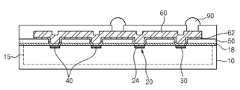
도 1은 본 발명의 일실시예에 의한 웨이퍼 레벨 반도체 패키지의 평면도이다. 도 2는 도 1의 I-I' 선을 따라 절단한 단면도이다.1 is a plan view of a wafer level semiconductor package according to an embodiment of the present invention. FIG. 2 is a cross-sectional view taken along the line II ′ of FIG. 1.
도 1을 참조하면, 웨이퍼 레벨 반도체 패키지(100)는 반도체 칩(10), 본딩 패드 그룹(20), 내부 회로 패턴(30), 추가 전원 패드(40), 절연막 패턴(50) 및 재배선(60)을 포함한다.Referring to FIG. 1, the wafer
반도체 칩(10)은, 예를 들어, 직육면체 형상을 갖는다. 직육면체 형상을 갖는 반도체 칩(10)은 상면 및 상면과 대향 하는 하면을 갖는다.The
반도체 칩(10)은 도 2에 도시된 회로부(15) 및 보호막 패턴(18)을 포함한다.The
회로부(15)는 데이터를 저장하기 위한 트랜지스터 및 커패시터 등을 포함하는 데이터 저장부(미도시) 및 데이터 저장부의 데이터를 처리하는 주변부(미도시)를 포함한다.The
보호막 패턴(18)은 반도체 칩(10)을 외부에서 인가된 충격 및 진동 등으로부터 보호한다. 보호막 패턴(18)은 산화막 및/또는 질화막일 수 있다. 보호막 패턴(18)의 개구에 의하여 후술 될 본딩 패드 그룹(20), 내부 회로 패턴(30) 및 추가 전원 패드(40)들은 각각 외부에 노출된다.The
본딩 패드 그룹(20)은 어드레스 신호, 데이터 신호 및 컨트롤 신호가 입력 또는 출력되는 데이터 패드(22) 및 반도체 칩을 작동시키기 위한 전원이 인가되는 전원 패드(24)를 포함한다. 본 실시예에서, 본딩 패드 그룹(20)은 다수개의 데이터 패드(22)들 및 다수개의 전원 패드(24)들을 포함할 수 있다.The
본딩 패드 그룹(20)에 포함된 전원 패드(24)는 반도체 칩(10)의 내부에 형성 된 내부 배선(미도시)을 이용하여 도 2에 도시된 회로부(15)로 전원을 제공한다. 본딩 패드 그룹(20)에 포함된 전원 패드(24)와 전기적으로 연결된 상기 내부 배선은 박막 처리 공정을 이용하여 제조되고 이로 인해 내부 배선은 비교적 높은 전기 저항을 갖는다.The
내부 회로 패턴(30)은 본딩 패드 그룹(20)의 일측 또는 본딩 패드 그룹(20)의 양쪽에 각각 배치될 수 있다. 내부 회로 패턴(30)은, 예를 들어, 반도체 칩 몸체(10)에 적어도 하나가 배치될 수 있다.The
내부 회로 패턴(30)은 반도체 칩(10) 내부에서 회로부(15)와 전기적으로 연결되며 내부 회로 패턴(30)은 본딩 패드 그룹(20)에 포함된 전원 패드(24)와 연결된 상기 내부 배선에 비하여 상대적으로 낮은 전기 저항을 갖는다.The
내부 회로 패턴(30)은 후술 될 재배선(60)과 전기적으로 연결되어 본딩 패드 그룹(20)에 포함된 전원 패드(24)의 개수의 증가 없이 충분한 전원을 회로부(15)로 제공할 수 있도록 한다.The
비록 내부 회로 패턴(30)을 통해 회로부(15)로 전원을 충분히 제공하더라도 반도체 칩의 데이터 집적도 및 반도체 칩의 데이터 처리 속도가 보다 향상될 경우, 반도체 칩의 특정 부분, 예를 들어, 반도체 칩의 가장자리 부분으로는 충분한 전원이 제공되지 않을 수 있다.Although sufficient power is provided to the
물론 내부 회로 패턴(30)의 개수를 증가 또는 내부 회로 패턴(30)의 길이를 증가시켜 반도체 칩에 전원을 충분히 제공할 수 있지만, 반도체 칩(10)에는 설계상 내부 회로 패턴(30)을 형성하기 어려운 부분이 존재하기 때문에 반도체 칩의 데이 터 집적도 및 반도체 칩의 데이터 처리 속도가 보다 향상될 경우, 내부 회로 패턴(30)만으로는 반도체 칩의 특정 부분으로 전원을 충분히 제공하기 어렵다.Although the number of the
추가 전원 패드(40)는 내부 회로 패턴(30)에 의하여 전원을 충분히 제공하기 어려운 반도체 칩 몸체의 특정 부분으로 전원을 제공할 수 있다.The
추가 전원 패드(40)는 본딩 패드 그룹(20)의 일측 또는 본딩 패드 그룹(20)의 양쪽에 배치될 수 있다. 추가 전원 패드(40)는, 예를 들어, 반도체 칩 몸체(10)에 적어도 하나가 배치될 수 있다.The
추가 전원 패드(40)는 본딩 패드 그룹(20)을 제외한 반도체 칩 몸체(10)의 소정 위치에 소정 개수로 형성될 수 있다. 즉, 추가 전원 패드(40)는 내부 회로 패턴(30)을 형성하기 어려운 위치에 자유롭게 형성될 수 있어 충분한 전원이 요구되는 회로부(15)에 충분한 전원을 제공할 수 있다.The
도 2를 참조하면, 절연막 패턴(50)은 반도체 칩 몸체(10)에 형성된 보호막 패턴(18) 상에 배치된다. 절연막 패턴(50)은, 예를 들어, 유기물을 포함하는 유기막일 수 있다.Referring to FIG. 2, the
재배선(60)은 절연막 패턴(50) 상에 배치된다. 재배선(60)은 단층막 구조를 가질 수 있다. 예를 들어, 재배선(60)은 금층(gold layer)일 수 있다. 이와 다르게, 재배선(60)은 복층막 구조를 가질 수 있다. 예를 들어, 재배선(60)은 구리층/니켈층/금층(Cu/Ni/Au), 구리층/금층(Cu/Au) 및 니켈층/금층(Ni/Au)을 가질 수 있다.The
재배선(60)은 씨드 금속 패턴(62)을 포함할 수 있다. 씨드 금속 패턴(62)으 로서 사용될 수 있는 물질의 예로서는, 티타늄, 니켈 및 바나듐 등을 들 수 있다.The
절연막 패턴(50) 상에 배치된 재배선(60)은 본딩 패드 그룹(20)에 포함된 전원 패드(24), 내부 회로 패턴(30) 및 추가 전원 패드(40) 중 적어도 2 개와 전기적으로 연결된다.The
예를 들어, 재배선(60)은 본딩 패드 그룹(20)에 포함된 전원 패드(24) 및 내부 회로 패턴(30)을 전기적으로 연결할 수 있다. 이때, 전원 패드(24) 및 내부 회로 패턴(30)과 전기적으로 연결된 재배선(60) 및 추가 전원 패드(40)에는 각각 볼 랜드 패턴(미도시)이 배치되어 재배선(60) 및 추가 전원 패드(40)에는 독립적으로 전원이 제공된다. 볼 랜드 패턴에는 전원을 제공하는 인쇄회로기판 및 볼 랜드 패턴을 전기적으로 연결하기 위한 솔더볼이 부착될 수 있다.For example, the
한편, 절연막 패턴(50) 상에 배치된 재배선(60)은 본딩 패드 그룹(20)에 포함된 전원 패드(24) 및 추가 전원 패드(40)를 전기적으로 연결할 수 있다. 이때, 전원 패드(24) 및 추가 전원 패드(40)와 전기적으로 연결된 재배선(60) 및 내부 회로 패턴(30)에는 각각 볼 랜드 패턴(미도시)들이 배치되어 재배선(60) 및 내부 회로 패턴(30)에는 독립적으로 전원이 제공된다. 볼 랜드 패턴에는 전원을 제공하는 인쇄회로기판 및 볼 랜드 패턴을 전기적으로 연결하기 위한 솔더볼이 부착될 수 있다.Meanwhile, the
한편, 절연막 패턴(50) 상에 배치된 재배선(60)은 추가 전원 패드(40) 및 내부 회로 패턴(30)과 전기적으로 연결될 수 있다. 이때, 추가 전원 패드(40) 및 내부 회로 패턴(30)을 전기적으로 연결하는 재배선(60) 및 본딩 패드 그룹(20)에 포함된 전원 패드(24)에는 각각 볼 랜드 패턴(미도시)이 배치되어 재배선(60) 및 전원 패드(24)에는 독립적으로 전원이 제공된다. 볼 랜드 패턴에는 전원을 제공하는 인쇄회로기판 및 볼 랜드 패턴을 전기적으로 연결하기 위한 솔더볼이 부착될 수 있다.Meanwhile, the
한편, 절연막 패턴(50) 상에 배치된 재배선(60)은 본딩 패드 그룹(20)에 포함된 전원 패드(24), 내부 회로 패턴(30), 추가 전원 패드(40)와 전기적으로 연결될 수 있다. 이때, 각 재배선(60)에는 볼 랜드 패턴(미도시)이 배치되어 재배선(60)에는 전원이 제공된다. 볼 랜드 패턴에는 전원을 제공하는 인쇄회로기판 및 볼 랜드 패턴을 전기적으로 연결하기 위한 솔더볼이 부착될 수 있다.Meanwhile, the
전원 패드(24), 내부 회로 패턴(30) 및 추가 전원 패드(40)와 전기적으로 연결된 재배선(60)에 전원이 인가되어 반도체 칩 몸체(10)의 회로부(15)에는 회로부를 구동하기에 충분한 전원을 제공할 수 있다.Power is applied to the
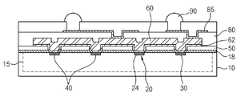
도 3은 본 발명의 다른 실시예에 의한 웨이퍼 레벨 반도체 패키지의 단면도이다. 3 is a cross-sectional view of a wafer level semiconductor package according to another embodiment of the present invention.
도 3을 참조하면, 반도체 칩 몸체(10)는 캡핑막 패턴(80), 볼 랜드 패턴(85) 및 솔더볼(90)을 포함할 수 있다.Referring to FIG. 3, the
캡핑막 패턴(80)은 절연막 패턴(50) 상에 배치된 재배선(60)의 일부를 노출하는 개구를 갖는다. 볼 랜드 패턴(85)은 캡핑막 패턴(80) 상에 배치되며 상기 개구를 통해 재배선(60)과 전기적으로 연결되고, 솔더볼(90)은 볼 랜드 패턴(85)과 전기적으로 접속된다.The
도 4 내지 도 8들은 본 발명의 일실시예에 의한 웨이퍼 레벨 반도체 패키지의 제조 공정을 도시한 평면도 및 단면도들이다.4 through 8 are plan and cross-sectional views illustrating a process of manufacturing a wafer level semiconductor package according to an embodiment of the present invention.
도 4는 본 발명에 의한 반도체 칩을 도시한 평면도이다. 도 5는 도 4의 II-II' 선을 따라 절단한 단면도이다.4 is a plan view showing a semiconductor chip according to the present invention. FIG. 5 is a cross-sectional view taken along the line II-II 'of FIG. 4.
도 4 및 도 5를 참조하면, 웨이퍼 레벨 반도체 패키지를 제조하기 위하여 먼저 반도체 소자 제조 공정에 의하여 반도체 칩(10)이 제조된다.4 and 5, a
반도체 소자 제조 공정에 의하여 반도체 칩(10)에는 데이터를 저장하는 데이터 저장부 및 데이터를 처리하는 데이터 처리부를 포함하는 회로부(15)가 형성되고, 반도체 칩(10)의 상면 중앙부에는 본딩 패드 그룹(20)이 형성된다. 본딩 패드 그룹(20)은 어드레스 신호, 데이터 신호 및 콘트롤 신호가 입력 또는 출력되는 데이터 패드(22) 및 전원이 인가되는 전원 패드(24)를 포함한다. 본딩 패드 그룹(20)의 양쪽에는 회로부(15)와 전기적으로 연결된 내부 회로 패턴(30)이 형성되고, 본딩 패드 그룹(20)의 양쪽에는 추가 전원 패드(40)들이 형성된다.In the semiconductor device manufacturing process, a
한편, 반도체 소자 제조 공정에 의하여, 반도체 칩(10)의 상면에는 보호막 패턴(18)이 형성된다. 보호막 패턴(18)은 산화막 및/또는 질화막일 수 있고, 보호막 패턴(18)은 본딩 패드 그룹(20)을 선택적으로 노출하는 개구를 포함한다.On the other hand, the
반도체 소자 제조 공정에 의하여 제조된 반도체 칩(10)은 한정된 개수의 전원 패드(24)를 포함하고, 이로 인해 반도체 칩(10)의 데이터 집적도 및 데이터 처리 속도가 증가 될 경우 회로부(15)로 전원을 충분히 제공하기 어렵다.The
도 6은 도 5에 도시된 보호막 패턴 상에 절연막 패턴을 형성한 것을 도시한 단면도이다.FIG. 6 is a cross-sectional view illustrating the formation of an insulating film pattern on the protective film pattern shown in FIG. 5.
도 6을 참조하면, 회로부(15)로 충분한 전원을 제공하기 위하여 본딩 패드 그룹(20)에 포함된 데이터 패드(22) 및 전원 패드(24)를 노출하는 개구를 갖는 보호막 패턴(18)은 다시 패터닝 되고, 이로 인해 내부 회로 패턴(30) 및 추가 전원 패드(40)들은 외부에 노출된다. 내부 회로 패턴(30) 및 추가 전원 패드(40)들은 각각 회로부(15)와 전기적으로 연결되어 회로부(15)에 충분한 전원을 제공한다.Referring to FIG. 6, the
보호막 패턴(18)을 패터닝 하여 내부 회로 패턴(30) 및 추가 전원 패드(40)들을 노출한 후, 보호막 패턴(18) 상에는 절연막(미도시)이 형성된다. 절연막은, 예를 들어, 유기막일 수 있다.After the
절연막이 형성된 후, 절연막 상에는 사진 공정 및 현상 공정을 포함하는 포토레지스트 패턴이 형성되고, 절연막은 포토레지스트 패턴을 식각 마스크로 이용하여 패터닝 되어 보호막 패턴(18) 상에는 내부 회로 패턴(30) 및 추가 전원 패드(40) 및 본딩 패드 그룹(20)을 노출하는 절연막 패턴(50)이 형성된다.After the insulating film is formed, a photoresist pattern including a photo process and a developing process is formed on the insulating film, and the insulating film is patterned by using the photoresist pattern as an etching mask, and the
도 7은 절연막 패턴 상에 씨드 금속층을 형성한 것을 도시한 단면도이다.7 is a cross-sectional view illustrating the formation of a seed metal layer on an insulating film pattern.
도 7을 참조하면, 절연막 패턴(50)이 형성된 후, 절연막 패턴(50) 상에는 전면적에 걸쳐 얇은 두께를 갖는 씨드 금속층(64)이 형성된다. 씨드 금속층(64)으로서 사용될 수 있는 물질의 예로서는 티타늄, 니켈 및 바나듐 등을 들 수 있다.Referring to FIG. 7, after the insulating
씨드 금속층(64)이 형성된 후, 씨드 금속층(64) 상에는 포토레지스트 패턴(66)이 형성된다. 포토레지스트 패턴(66)은 씨드 금속층(64)의 일부를 노출하는 개구(68)를 포함한다.After the
포토레지스트 패턴(66)의 개구(68)는, 예를 들어, 전원 패드(24) 및 내부 회로 패턴(30)을 연결하는 라인 형상을 가질 수 있다.The
한편, 포토레지스트 패턴(66)의 개구(68)는, 예를 들어, 전원 패드(24) 및 추가 전원 패드(40)를 연결하는 라인 형상을 가질 수 있다.On the other hand, the
한편, 포토레지스트 패턴(66)의 개구(68)는, 예를 들어, 추가 전원 패드(40) 및 내부 회로 패턴(30)을 연결하는 라인 형상을 가질 수 있다.On the other hand, the
한편, 포토레지스트 패턴(66)의 개구(68)는, 예를 들어, 전원 패드(24), 추가 전원 패드(40) 및 내부 회로 패턴(30)을 연결하는 라인 형상을 가질 수 있다.The
도 8은 본 발명의 일실시예에 의한 재배선을 도시한 단면도이다.8 is a cross-sectional view showing a rewiring according to an embodiment of the present invention.
도 8을 참조하면, 개구(68)를 갖는 포토레지스트 패턴(66)이 씨드 금속층(64) 상에 형성된 후, 씨드 금속층(64)을 이용하여 도금 공정이 수행되어 씨드 금속층(64) 상에는 재배선(60)이 형성된다.Referring to FIG. 8, after the
본 실시예에서, 재배선(60)은 전원 패드(24) 및 내부 회로 패턴(30)을 전기적으로 연결할 수 있다. 이와 다르게, 재배선(60)은 전원 패드(24) 및 추가 전원 패드(40)를 전기적으로 연결할 수 있다. 이와 다르게, 재배선(60)은 추가 전원 패드(40) 및 내부 회로 패턴(30)을 연결할 수 있다. 이와 다르게, 재배선(60)은 전원 패드(24), 추가 전원 패드(40) 및 내부 회로 패턴(30)을 전기적으로 연결할 수 있다.In the present embodiment, the
한편, 재배선(60)을 형성할 때, 재배선(60)과 동일한 평면상에 볼 랜드 패턴(미도시)이 형성될 수 있고, 볼 랜드 패턴에는 솔더볼(65)이 접속될 수 있다. 볼 랜드 패턴을 통해 회로부(15)로 제공될 전원이 제공된다.Meanwhile, when the
재배선(60)이 형성된 후, 포토레지스트 패턴(68)은 씨드 금속층(64)으로부터 제거되고, 씨드 금속층(64)은 재배선(60)을 식각 마스크로 이용하여 패터닝 되어 재배선(60)의 하부에는 씨드 금속 패턴(62)이 형성된다.After the
이에 더하여, 도 3에 도시된 바와 같이 재배선(60)의 일부를 노출하는 개구를 갖는 캡핑막 패턴(85)을 형성하고, 캡핑막 패턴(85) 상에 볼 랜드 패턴(85)을 형성한 후, 볼 랜드 패턴(85)에 솔더볼을 어탯치하여도 무방하다.In addition, as shown in FIG. 3, a
이상에서 상세하게 설명한 바에 의하면, 저전압 작동 특성을 만족하면서 충분한 전원을 반도체 칩에 제공하여 반도체 칩의 성능을 크게 향상시키는 효과를 갖는다.As described in detail above, the semiconductor chip has an effect of greatly improving the performance of the semiconductor chip by providing sufficient power to the semiconductor chip while satisfying the low voltage operating characteristics.
앞서 설명한 본 발명의 상세한 설명에서는 본 발명의 실시예들을 참조하여 설명하였지만, 해당 기술분야의 숙련된 당업자 또는 해당 기술분야에 통상의 지식을 갖는 자라면 후술 될 특허청구범위에 기재된 본 발명의 사상 및 기술 영역으로부터 벗어나지 않는 범위 내에서 본 발명을 다양하게 수정 및 변경시킬 수 있음을 이해할 수 있을 것이다.In the detailed description of the present invention described above with reference to the embodiments of the present invention, those skilled in the art or those skilled in the art having ordinary knowledge in the scope of the present invention described in the claims and It will be appreciated that various modifications and variations can be made in the present invention without departing from the scope of the art.
도 1은 본 발명의 일실시예에 의한 웨이퍼 레벨 반도체 패키지의 평면도이다.1 is a plan view of a wafer level semiconductor package according to an embodiment of the present invention.
도 2는 도 1의 I-I' 선을 따라 절단한 단면도이다.FIG. 2 is a cross-sectional view taken along the line II ′ of FIG. 1.
도 3은 본 발명의 다른 실시예에 의한 웨이퍼 레벨 반도체 패키지의 단면도이다.3 is a cross-sectional view of a wafer level semiconductor package according to another embodiment of the present invention.
도 4 내지 도 8들은 본 발명의 일실시예에 의한 웨이퍼 레벨 반도체 패키지의 제조 공정을 도시한 평면도 및 단면도들이다.4 through 8 are plan and cross-sectional views illustrating a process of manufacturing a wafer level semiconductor package according to an embodiment of the present invention.
Claims (14)
Translated fromKoreanPriority Applications (5)
| Application Number | Priority Date | Filing Date | Title |
|---|---|---|---|
| KR1020070123755AKR100910231B1 (en) | 2007-11-30 | 2007-11-30 | Wafer level semiconductor package and method for manufacturing same |
| US11/965,087US7705457B2 (en) | 2007-11-30 | 2007-12-27 | Wafer level semiconductor package and method for manufacturing the same |
| TW097101079ATWI398940B (en) | 2007-11-30 | 2008-01-11 | Wafer level semiconductor package and method for manufacturing the same |
| JP2008018370AJP5086115B2 (en) | 2007-11-30 | 2008-01-29 | Wafer level semiconductor package and manufacturing method thereof |
| CN2008100830219ACN101447469B (en) | 2007-11-30 | 2008-03-18 | Wafer level semiconductor package and method for manufacturing the same |
Applications Claiming Priority (1)
| Application Number | Priority Date | Filing Date | Title |
|---|---|---|---|
| KR1020070123755AKR100910231B1 (en) | 2007-11-30 | 2007-11-30 | Wafer level semiconductor package and method for manufacturing same |
Publications (2)
| Publication Number | Publication Date |
|---|---|
| KR20090056551A KR20090056551A (en) | 2009-06-03 |
| KR100910231B1true KR100910231B1 (en) | 2009-07-31 |
Family
ID=40674909
Family Applications (1)
| Application Number | Title | Priority Date | Filing Date |
|---|---|---|---|
| KR1020070123755AExpired - Fee RelatedKR100910231B1 (en) | 2007-11-30 | 2007-11-30 | Wafer level semiconductor package and method for manufacturing same |
Country Status (5)
| Country | Link |
|---|---|
| US (1) | US7705457B2 (en) |
| JP (1) | JP5086115B2 (en) |
| KR (1) | KR100910231B1 (en) |
| CN (1) | CN101447469B (en) |
| TW (1) | TWI398940B (en) |
Families Citing this family (10)
| Publication number | Priority date | Publication date | Assignee | Title |
|---|---|---|---|---|
| JP4776975B2 (en)* | 2005-05-11 | 2011-09-21 | キヤノン株式会社 | Imaging device |
| JP2010140981A (en)* | 2008-12-10 | 2010-06-24 | Elpida Memory Inc | Chip structure, chip laminated structure, semiconductor package structure, and memory |
| KR101169531B1 (en)* | 2009-07-03 | 2012-07-27 | 가부시키가이샤 테라미크로스 | Semiconductor construct and manufacturing method thereof as well as semiconductor device and manufacturing method thereof |
| KR101936039B1 (en) | 2012-10-30 | 2019-01-08 | 삼성전자 주식회사 | Semiconductor device |
| CN110767625B (en)* | 2018-07-25 | 2024-07-23 | 盛合晶微半导体(江阴)有限公司 | RDL metal wire manufacturing method and structure |
| CN109065515B (en)* | 2018-08-31 | 2024-06-11 | 合肥矽迈微电子科技有限公司 | Chip packaging structure with high conductivity and low resistance and preparation method thereof |
| US20200312732A1 (en) | 2018-09-14 | 2020-10-01 | Mediatek Inc. | Chip scale package structure and method of forming the same |
| US11450606B2 (en) | 2018-09-14 | 2022-09-20 | Mediatek Inc. | Chip scale package structure and method of forming the same |
| KR102179167B1 (en)* | 2018-11-13 | 2020-11-16 | 삼성전자주식회사 | Semiconductor package |
| IT202200001646A1 (en)* | 2022-02-01 | 2023-08-01 | St Microelectronics Srl | Process for manufacturing semiconductor devices and corresponding semiconductor device |
Citations (2)
| Publication number | Priority date | Publication date | Assignee | Title |
|---|---|---|---|---|
| KR100583966B1 (en) | 2004-06-08 | 2006-05-26 | 삼성전자주식회사 | Integrated Circuit Packages With Repositioned Metal Wiring and Methods of Manufacturing the Same |
| KR20060100885A (en)* | 2005-03-18 | 2006-09-21 | 삼성전자주식회사 | Semiconductor chips having repositioned power supply / grounding lines directly connected to the power supply / grounding lines of an internal circuit and manufacturing methods thereof |
Family Cites Families (12)
| Publication number | Priority date | Publication date | Assignee | Title |
|---|---|---|---|---|
| KR100361084B1 (en)* | 2000-01-21 | 2002-11-18 | 주식회사 하이닉스반도체 | Semiconductor package and fabricating method thereof |
| TW577152B (en)* | 2000-12-18 | 2004-02-21 | Hitachi Ltd | Semiconductor integrated circuit device |
| JP3939504B2 (en)* | 2001-04-17 | 2007-07-04 | カシオ計算機株式会社 | Semiconductor device, method for manufacturing the same, and mounting structure |
| JP2004221359A (en)* | 2003-01-15 | 2004-08-05 | Matsushita Electric Ind Co Ltd | Semiconductor device |
| US6917105B2 (en)* | 2003-06-03 | 2005-07-12 | Micrel, Incorporated | Integrating chip scale packaging metallization into integrated circuit die structures |
| SG115753A1 (en)* | 2004-03-15 | 2005-10-28 | Yamaha Corp | Semiconductor element and wafer level chip size package therefor |
| JP4072523B2 (en)* | 2004-07-15 | 2008-04-09 | 日本電気株式会社 | Semiconductor device |
| JP2006303036A (en)* | 2005-04-18 | 2006-11-02 | Fujikura Ltd | Semiconductor device |
| JP4449824B2 (en)* | 2005-06-01 | 2010-04-14 | カシオ計算機株式会社 | Semiconductor device and its mounting structure |
| CN101278394B (en)* | 2005-10-03 | 2010-05-19 | 罗姆股份有限公司 | Semiconductor device |
| KR100729362B1 (en)* | 2006-04-27 | 2007-06-15 | 삼성전자주식회사 | A semiconductor package having a heat dissipation device directly connected to an internal circuit and a method of manufacturing the same |
| KR100794658B1 (en)* | 2006-07-07 | 2008-01-14 | 삼성전자주식회사 | Method of manufacturing semiconductor chip, semiconductor chip formed thereby and chip stack package comprising same |
- 2007
- 2007-11-30KRKR1020070123755Apatent/KR100910231B1/ennot_activeExpired - Fee Related
- 2007-12-27USUS11/965,087patent/US7705457B2/enactiveActive
- 2008
- 2008-01-11TWTW097101079Apatent/TWI398940B/ennot_activeIP Right Cessation
- 2008-01-29JPJP2008018370Apatent/JP5086115B2/ennot_activeExpired - Fee Related
- 2008-03-18CNCN2008100830219Apatent/CN101447469B/ennot_activeExpired - Fee Related
Patent Citations (2)
| Publication number | Priority date | Publication date | Assignee | Title |
|---|---|---|---|---|
| KR100583966B1 (en) | 2004-06-08 | 2006-05-26 | 삼성전자주식회사 | Integrated Circuit Packages With Repositioned Metal Wiring and Methods of Manufacturing the Same |
| KR20060100885A (en)* | 2005-03-18 | 2006-09-21 | 삼성전자주식회사 | Semiconductor chips having repositioned power supply / grounding lines directly connected to the power supply / grounding lines of an internal circuit and manufacturing methods thereof |
Also Published As
| Publication number | Publication date |
|---|---|
| JP5086115B2 (en) | 2012-11-28 |
| TW200924149A (en) | 2009-06-01 |
| US20090140424A1 (en) | 2009-06-04 |
| TWI398940B (en) | 2013-06-11 |
| CN101447469B (en) | 2011-01-26 |
| JP2009135389A (en) | 2009-06-18 |
| CN101447469A (en) | 2009-06-03 |
| KR20090056551A (en) | 2009-06-03 |
| US7705457B2 (en) | 2010-04-27 |
Similar Documents
| Publication | Publication Date | Title |
|---|---|---|
| KR100910231B1 (en) | Wafer level semiconductor package and method for manufacturing same | |
| JP4897451B2 (en) | Semiconductor device | |
| JP3351706B2 (en) | Semiconductor device and method of manufacturing the same | |
| TWI856192B (en) | Semiconductor package | |
| KR102589736B1 (en) | Semiconductor chip and Semiconductor package including the same | |
| KR100876899B1 (en) | Semiconductor package | |
| KR20090002644A (en) | Semiconductor device having through electrode and method of manufacturing same | |
| KR20180011445A (en) | Solid state drive package | |
| JP2009033108A (en) | Semiconductor package, stacked wafer level package having the same and method of manufacturing stacked wafer level package | |
| JP4955488B2 (en) | Semiconductor device and manufacturing method thereof | |
| KR20190119474A (en) | Chip stack package | |
| KR100833194B1 (en) | Semiconductor package and manufacturing method in which wiring layer of semiconductor chip is directly connected to substrate | |
| KR20100095901A (en) | Stack type semiconductor package | |
| JP2008109138A (en) | Layered chip package and method for manufacturing the package | |
| CN107301954A (en) | Manufacturing method of packaging substrate | |
| US20220384325A1 (en) | Semiconductor package and method for fabricating the same | |
| JP2007266567A (en) | Semiconductor package with high speed and high performance | |
| KR102509049B1 (en) | Fan out package including vertically stacked chips | |
| CN101252107A (en) | Semiconductor package structure and manufacturing method thereof | |
| JP2005150578A (en) | Semiconductor device and its manufacturing method | |
| JP2004260074A (en) | Semiconductor device, method of manufacturing semiconductor device and method of mounting the same, circuit board, and electronic device | |
| KR101055453B1 (en) | Semiconductor package having heat sink and manufacturing method thereof | |
| KR100650635B1 (en) | Semiconductor device and manufacturing method thereof | |
| JP5000130B2 (en) | Semiconductor chip | |
| JP4728079B2 (en) | Semiconductor device substrate and semiconductor device |
Legal Events
| Date | Code | Title | Description |
|---|---|---|---|
| A201 | Request for examination | ||
| PA0109 | Patent application | St.27 status event code:A-0-1-A10-A12-nap-PA0109 | |
| PA0201 | Request for examination | St.27 status event code:A-1-2-D10-D11-exm-PA0201 | |
| D13-X000 | Search requested | St.27 status event code:A-1-2-D10-D13-srh-X000 | |
| D14-X000 | Search report completed | St.27 status event code:A-1-2-D10-D14-srh-X000 | |
| E902 | Notification of reason for refusal | ||
| PE0902 | Notice of grounds for rejection | St.27 status event code:A-1-2-D10-D21-exm-PE0902 | |
| P11-X000 | Amendment of application requested | St.27 status event code:A-2-2-P10-P11-nap-X000 | |
| P13-X000 | Application amended | St.27 status event code:A-2-2-P10-P13-nap-X000 | |
| PG1501 | Laying open of application | St.27 status event code:A-1-1-Q10-Q12-nap-PG1501 | |
| E701 | Decision to grant or registration of patent right | ||
| PE0701 | Decision of registration | St.27 status event code:A-1-2-D10-D22-exm-PE0701 | |
| GRNT | Written decision to grant | ||
| PR0701 | Registration of establishment | St.27 status event code:A-2-4-F10-F11-exm-PR0701 | |
| PR1002 | Payment of registration fee | St.27 status event code:A-2-2-U10-U11-oth-PR1002 Fee payment year number:1 | |
| PG1601 | Publication of registration | St.27 status event code:A-4-4-Q10-Q13-nap-PG1601 | |
| PN2301 | Change of applicant | St.27 status event code:A-5-5-R10-R13-asn-PN2301 St.27 status event code:A-5-5-R10-R11-asn-PN2301 | |
| FPAY | Annual fee payment | Payment date:20120625 Year of fee payment:4 | |
| PR1001 | Payment of annual fee | St.27 status event code:A-4-4-U10-U11-oth-PR1001 Fee payment year number:4 | |
| PN2301 | Change of applicant | St.27 status event code:A-5-5-R10-R13-asn-PN2301 St.27 status event code:A-5-5-R10-R11-asn-PN2301 | |
| LAPS | Lapse due to unpaid annual fee | ||
| PC1903 | Unpaid annual fee | St.27 status event code:A-4-4-U10-U13-oth-PC1903 Not in force date:20130725 Payment event data comment text:Termination Category : DEFAULT_OF_REGISTRATION_FEE | |
| PC1903 | Unpaid annual fee | St.27 status event code:N-4-6-H10-H13-oth-PC1903 Ip right cessation event data comment text:Termination Category : DEFAULT_OF_REGISTRATION_FEE Not in force date:20130725 | |
| PN2301 | Change of applicant | St.27 status event code:A-5-5-R10-R13-asn-PN2301 St.27 status event code:A-5-5-R10-R11-asn-PN2301 |