KR100909970B1 - Camera module - Google Patents
Camera moduleDownload PDFInfo
- Publication number
- KR100909970B1 KR100909970B1KR1020070111011AKR20070111011AKR100909970B1KR 100909970 B1KR100909970 B1KR 100909970B1KR 1020070111011 AKR1020070111011 AKR 1020070111011AKR 20070111011 AKR20070111011 AKR 20070111011AKR 100909970 B1KR100909970 B1KR 100909970B1
- Authority
- KR
- South Korea
- Prior art keywords
- image sensor
- camera module
- housing
- conductive
- sensor package
- Prior art date
- Legal status (The legal status is an assumption and is not a legal conclusion. Google has not performed a legal analysis and makes no representation as to the accuracy of the status listed.)
- Active
Links
Images


Classifications
- H—ELECTRICITY
- H04—ELECTRIC COMMUNICATION TECHNIQUE
- H04N—PICTORIAL COMMUNICATION, e.g. TELEVISION
- H04N23/00—Cameras or camera modules comprising electronic image sensors; Control thereof
- H04N23/50—Constructional details
- H04N23/52—Elements optimising image sensor operation, e.g. for electromagnetic interference [EMI] protection or temperature control by heat transfer or cooling elements
- H—ELECTRICITY
- H05—ELECTRIC TECHNIQUES NOT OTHERWISE PROVIDED FOR
- H05K—PRINTED CIRCUITS; CASINGS OR CONSTRUCTIONAL DETAILS OF ELECTRIC APPARATUS; MANUFACTURE OF ASSEMBLAGES OF ELECTRICAL COMPONENTS
- H05K1/00—Printed circuits
- H05K1/02—Details
- H05K1/0213—Electrical arrangements not otherwise provided for
- H05K1/0216—Reduction of cross-talk, noise or electromagnetic interference
- H05K1/0218—Reduction of cross-talk, noise or electromagnetic interference by printed shielding conductors, ground planes or power plane
- H—ELECTRICITY
- H04—ELECTRIC COMMUNICATION TECHNIQUE
- H04N—PICTORIAL COMMUNICATION, e.g. TELEVISION
- H04N23/00—Cameras or camera modules comprising electronic image sensors; Control thereof
- H04N23/50—Constructional details
- H04N23/54—Mounting of pick-up tubes, electronic image sensors, deviation or focusing coils
- G—PHYSICS
- G03—PHOTOGRAPHY; CINEMATOGRAPHY; ANALOGOUS TECHNIQUES USING WAVES OTHER THAN OPTICAL WAVES; ELECTROGRAPHY; HOLOGRAPHY
- G03B—APPARATUS OR ARRANGEMENTS FOR TAKING PHOTOGRAPHS OR FOR PROJECTING OR VIEWING THEM; APPARATUS OR ARRANGEMENTS EMPLOYING ANALOGOUS TECHNIQUES USING WAVES OTHER THAN OPTICAL WAVES; ACCESSORIES THEREFOR
- G03B17/00—Details of cameras or camera bodies; Accessories therefor
- G03B17/02—Bodies
- H—ELECTRICITY
- H04—ELECTRIC COMMUNICATION TECHNIQUE
- H04N—PICTORIAL COMMUNICATION, e.g. TELEVISION
- H04N23/00—Cameras or camera modules comprising electronic image sensors; Control thereof
- H04N23/57—Mechanical or electrical details of cameras or camera modules specially adapted for being embedded in other devices
- H—ELECTRICITY
- H10—SEMICONDUCTOR DEVICES; ELECTRIC SOLID-STATE DEVICES NOT OTHERWISE PROVIDED FOR
- H10F—INORGANIC SEMICONDUCTOR DEVICES SENSITIVE TO INFRARED RADIATION, LIGHT, ELECTROMAGNETIC RADIATION OF SHORTER WAVELENGTH OR CORPUSCULAR RADIATION
- H10F39/00—Integrated devices, or assemblies of multiple devices, comprising at least one element covered by group H10F30/00, e.g. radiation detectors comprising photodiode arrays
- H10F39/10—Integrated devices
- H10F39/12—Image sensors
- H—ELECTRICITY
- H05—ELECTRIC TECHNIQUES NOT OTHERWISE PROVIDED FOR
- H05K—PRINTED CIRCUITS; CASINGS OR CONSTRUCTIONAL DETAILS OF ELECTRIC APPARATUS; MANUFACTURE OF ASSEMBLAGES OF ELECTRICAL COMPONENTS
- H05K2201/00—Indexing scheme relating to printed circuits covered by H05K1/00
- H05K2201/10—Details of components or other objects attached to or integrated in a printed circuit board
- H05K2201/10007—Types of components
- H05K2201/10121—Optical component, e.g. opto-electronic component
- H—ELECTRICITY
- H05—ELECTRIC TECHNIQUES NOT OTHERWISE PROVIDED FOR
- H05K—PRINTED CIRCUITS; CASINGS OR CONSTRUCTIONAL DETAILS OF ELECTRIC APPARATUS; MANUFACTURE OF ASSEMBLAGES OF ELECTRICAL COMPONENTS
- H05K2201/00—Indexing scheme relating to printed circuits covered by H05K1/00
- H05K2201/10—Details of components or other objects attached to or integrated in a printed circuit board
- H05K2201/10227—Other objects, e.g. metallic pieces
- H05K2201/10371—Shields or metal cases
- H—ELECTRICITY
- H05—ELECTRIC TECHNIQUES NOT OTHERWISE PROVIDED FOR
- H05K—PRINTED CIRCUITS; CASINGS OR CONSTRUCTIONAL DETAILS OF ELECTRIC APPARATUS; MANUFACTURE OF ASSEMBLAGES OF ELECTRICAL COMPONENTS
- H05K2201/00—Indexing scheme relating to printed circuits covered by H05K1/00
- H05K2201/10—Details of components or other objects attached to or integrated in a printed circuit board
- H05K2201/10613—Details of electrical connections of non-printed components, e.g. special leads
- H05K2201/10621—Components characterised by their electrical contacts
- H05K2201/10734—Ball grid array [BGA]; Bump grid array
Landscapes
- Engineering & Computer Science (AREA)
- Multimedia (AREA)
- Signal Processing (AREA)
- Physics & Mathematics (AREA)
- Electromagnetism (AREA)
- Microelectronics & Electronic Packaging (AREA)
- General Physics & Mathematics (AREA)
- Studio Devices (AREA)
- Transforming Light Signals Into Electric Signals (AREA)
Abstract
Translated fromKoreanDescription
Translated fromKorean본 발명은 카메라 모듈에 관한 것으로서, 보다 상세하게는 모듈 내에서 발생되는 전자파가 외부로 방사되는 것을 방지하고, 외부의 전자파나 노이즈가 모듈 내부로 유입되는 것을 방지하는 구조를 갖는 EMC 차폐용 카메라 모듈에 관한 것이다.The present invention relates to a camera module, and more particularly, an EMC shielding camera module having a structure for preventing electromagnetic waves generated in the module from being radiated to the outside and preventing external electromagnetic waves or noise from flowing into the module. It is about.
전자 부품의 디지털화 및 사용하는 클럭(clock) 주파수의 속도가 높아짐에 따라 전자기파로 인한 무선통신에서의 채널간 상호 간섭, 주파수 스펙트럼 효용, 정보통신 네트워크의 신뢰성 등의 문제가 발생할 수 있으며 나아가 인체 등 생물 생태계에 대한 전자기파 에너지의 영향이 보다 중요한 문제가 되고 있다. 즉, 전자 부품들의 전자기적 양립성 또는 전자기적 적합성(EMC ; Electro-Magnetic Compatibility)의 개념이 중요해지고 있다. 전자기적 양립성의 하부 개념으로 전자기파 장애(EMI;EM Interference)와 전자기파 내성(EMS;EM Susceptibility)이 있다. 전자기파 장애는 제품으로부터 방사되는 RF 에너지 및 노이즈에 의해서 주변에 위치해 있는 다른 제품에 악영향을 미치는 현상을 의미하며, 전자기파 내성은 이와 반대되는 개념으로써 주변에 존재하는 모든 RF 에너지 및 노이즈 또는 정전기에 의해서 제품의 정상동작에 영향을 받지 않을 수 있는 제품의 자체의 내성을 의 미한다. 이하에서 전자기파를 차폐한다는 의미는 전자기파 장애를 최소화하고 전자기파 내성을 최대화하는 것을 의미한다.As the digitization of electronic components and the speed of the clock frequency used increase, problems such as mutual interference between channels, frequency spectrum utility, and reliability of telecommunication networks due to electromagnetic waves may occur. The impact of electromagnetic energy on ecosystems is becoming more important. That is, the concept of electromagnetic compatibility or electro-magnetic compatibility (EMC) of electronic components is becoming important. Underlying electromagnetic compatibility is electromagnetic interference (EMI) and electromagnetic susceptibility (EMS). Electromagnetic interference refers to a phenomenon that adversely affects other products located nearby by RF energy and noise radiated from the product, and electromagnetic immunity is the opposite concept. Means immunity of the product itself that may not be affected by normal operation. Hereinafter, shielding electromagnetic waves means minimizing electromagnetic interference and maximizing electromagnetic resistance.
특히, 휴대폰 내부에는 많은 소자들이 내장됨에 따라 소자간 전자기파의 차폐가 요구된다. 휴대폰 내부에 배치되는 카메라 모듈의 경우 주변의 소자들간의 전자기파를 차폐하기 위해 몇 가지 접지 구조가 제안되고 있다. 카메라 모듈이 소켓(socket) 타입인 경우에는 카메라 모듈의 하우징이 소켓을 통해 연결되므로 접지가 용이하지만, FPCB(Flexible Printed Circuit Board) 타입이나 BGA(Ball Grid Array) 타입인 경우 휴대폰 메인 기판과 카메라 모듈의 하우징을 좁은 실장 공간에서 효과적으로 연결하는 것이 용이하지 않는 문제점이 있다.In particular, as many devices are built into a mobile phone, shielding of electromagnetic waves between devices is required. In the case of a camera module disposed inside a mobile phone, several grounding structures have been proposed to shield electromagnetic waves between peripheral devices. If the camera module is socket type, the housing of the camera module is connected through the socket, so it is easy to ground.However, in case of FPCB (Flexible Printed Circuit Board) or BGA (Ball Grid Array) type, the mobile phone main board and camera module There is a problem that it is not easy to effectively connect the housings in the narrow mounting space.
본 발명이 이루고자 하는 기술적 과제는 전자기파를 효과적으로 차폐하면서 메인 기판의 실장 면적을 최소화할 수 있는 카메라 모듈을 제공하는 데 있다.The present invention is to provide a camera module that can minimize the mounting area of the main substrate while effectively shielding electromagnetic waves.
상기 기술적 과제를 달성하기 위한 본 발명의 일실시예에 따른 카메라 모듈은 하나 이상의 렌즈를 포함하는 렌즈부; 상기 렌즈부를 통과한 광이 결상되는 이미지 영역을 구비하는 이미지 센서 칩을 포함하는 이미지 센서 패키지; 상기 렌즈부와 상기 이미지 센서 패키지의 각각의 측면을 둘러싸며, 상기 이미지 센서 패키지와 전기적으로 연결되며, 도전성 물질을 포함하여 형성되는 하우징; 및 이미지 센서 패키지의 하부에 배치되며, 상기 이미지 센서 패키지와 전자기기의 메인 기판을 전기적으로 연결하는 구조물;을 포함한다.Camera module according to an embodiment of the present invention for achieving the above technical problem is a lens unit including one or more lenses; An image sensor package including an image sensor chip having an image area in which light passing through the lens unit is formed; A housing surrounding each side of the lens unit and the image sensor package, the housing being electrically connected to the image sensor package and formed of a conductive material; And a structure disposed under the image sensor package and electrically connecting the image sensor package and the main substrate of the electronic device.
상기 이미지 센서 패키지는 상기 이미지 센서 칩이 상면에 실장되는 제1 기판; 및 상기 이미지 센서 칩과 상기 제1 기판을 전기적으로 연결하는 와이어;를 더 포함할 수 있다. 또는 상기 이미지 센서 패키지는 상기 이미지 센서 칩을 포함하는 이미지 센서 칩 스케일 패키지(Image Sensor CSP)일 수 있다. 상기 메인 기판은 PWB(Printed Wire Board), 플렉시블 PWB(Flexible PWB) 또는 리지드 플렉시블 PWB(Rigid Flexible PWB)일 수 있다.The image sensor package may include a first substrate on which the image sensor chip is mounted on an upper surface thereof; And a wire electrically connecting the image sensor chip and the first substrate. Alternatively, the image sensor package may be an image sensor chip scale package (Image Sensor CSP) including the image sensor chip. The main substrate may be a printed wire board (PWB), a flexible PWB (rigid PWB), or a rigid flexible PWB (rigid flexible PWB).
상기 이미지 센서 패키지의 하면에는 도전성의 제1 접지 패드가 형성되며, 상기 제1 접지 패드와 상기 하우징은 도전성 페이스트(conductive paste)에 의해 전기적으로 연결될 수 있다. 상기 도전성 페이스트는 상기 하우징의 하면에서부터 상기 제1 접지 패드까지 신장하여 형성될 수 있으며, 상기 제1 접지 패드 하에 형성된 솔더볼을 더 포함하고, 상기 솔더볼에 의해 상기 이미지 센서 패키지와 상기 메인 기판이 전기적으로 연결될 수 있다. 상기 하우징은 상기 광이 통과하지 않는 상기 렌즈부의 상면 외곽부까지 신장할 수 있다. 상기 하우징은 도전성 물질로 형성되는 몸체를 포함하며, 상기 하우징의 내부면이 상기 몸체 상에 형성된 절연막으로 형성될 수 있다.A conductive first ground pad may be formed on a bottom surface of the image sensor package, and the first ground pad and the housing may be electrically connected by a conductive paste. The conductive paste may be formed to extend from a lower surface of the housing to the first ground pad, and further include solder balls formed under the first ground pad, wherein the image sensor package and the main substrate are electrically connected to each other by the solder balls. Can be connected. The housing may extend to an outer edge of the upper surface of the lens unit through which the light does not pass. The housing may include a body formed of a conductive material, and an inner surface of the housing may be formed of an insulating film formed on the body.
상기 기술적 과제를 달성하기 위한 본 발명의 다른 실시예에 따른 카메라 모듈은 상기 하우징은 절연성 물질로 형성되는 몸체와 상기 몸체의 외부면에 형성된 도전막을 포함할 수 있다. 상기 도전막은 상기 몸체의 측면에서 상기 몸체의 하면까지 신장하여 형성될 수 있다. 상기 이미지 센서 패키지의 하면에는 도전성의 제1 접지 패드가 형성되며, 상기 도전막은 상기 몸체의 측면에서 상기 몸체의 하면을 지나서 상기 제1 접지 패드까지 신장하여 형성되며, 상기 제1 접지 패드 하의 상기 도전막 내에 형성된 비아홀을 채워서 형성되는 도전성 페이스트를 더 포함할 수 있다.The camera module according to another embodiment of the present invention for achieving the technical problem may include a body formed of an insulating material and a conductive film formed on the outer surface of the body. The conductive layer may be formed to extend from the side of the body to the lower surface of the body. A conductive first ground pad is formed on a bottom surface of the image sensor package, and the conductive layer is formed to extend from the side surface of the body to the first ground pad beyond the bottom surface of the body, and to conduct the conductive under the first ground pad. The method may further include a conductive paste formed by filling a via hole formed in the film.
상기 기술적 과제를 달성하기 위한 본 발명의 또 다른 실시예에 따른 카메라 모듈은 상기 메인 기판은 도전성의 제2 접지 패드를 더 포함하고, 상기 하우징은 상기 메인 기판까지 신장하여 상기 제2 접지 패드와 전기적으로 연결될 수 있다.According to another aspect of the present invention, there is provided a camera module, wherein the main substrate further includes a conductive second ground pad, and the housing extends to the main substrate to electrically connect with the second ground pad. Can be connected.
본 발명에 의한 카메라 모듈에 따르면, 전자기파를 효과적을 차폐할 수 있는 카메라 모듈을 제공할 수 있다.According to the camera module according to the present invention, it is possible to provide a camera module that can effectively shield the electromagnetic waves.
첨부된 도면을 참조하여 본 발명의 바람직한 실시예들을 상세히 설명하기로 한다. 그러나, 본 발명은 여기서 설명되어지는 실시예들에 한정되지 않고 다른 형태로 구체화될 수도 있다. 오히려, 여기서 소개되는 실시예들은 개시된 내용이 철저하고 완전해질 수 있도록 그리고 당업자에게 본 발명의 사상이 충분히 전달될 수 있도록 하기 위해 제공되어지는 것이다. 도면들에 있어서, 층 및 영역들의 두께는 명확성을 기하여 위하여 과장되어진 것이다.With reference to the accompanying drawings will be described in detail preferred embodiments of the present invention. However, the present invention is not limited to the embodiments described herein and may be embodied in other forms. Rather, the embodiments introduced herein are provided to ensure that the disclosed subject matter is thorough and complete, and that the scope of the invention to those skilled in the art will fully convey. In the drawings, the thicknesses of layers and regions are exaggerated for clarity.
명세서 전체에 걸쳐서 동일한 참조번호들은 동일한 구성요소들을 나타낸다. 명세서 전체에 걸쳐서 막, 영역, 또는 기판등과 같은 하나의 구성요소가 또 다른 구성요소 "상에" 위치한다고 언급할 때는, 상기 하나의 구성요소가 다른 구성요소에 직접 접촉하거나 중간에 개재되는 구성요소들이 존재할 수 있다고 해석될 수 있다. 또한, "상의" 또는 "위의" 및 "하의" 또는 "아래의"와 같은 상대적인 용어들은 도면들에서 도해되는 것처럼 다른 요소들에 대한 어떤 요소들의 관계를 기술하기 위해 여기에서 사용될 수 있다. 상대적 용어들은 도면들에서 묘사되는 방향에 추가하여 소자의 다른 방향들을 포함하는 것을 의도한다고 이해될 수 있다. 예를 들어, 도면들에서 소자가 뒤집어 진다면(turned over), 다른 요소들의 상부의 면 상에 존재하는 것으로 묘사되는 요소들은 상기 다른 요소들의 하부의 면 상에 방향을 가지게 된다. 그러므로, 예로써 든 "상의"라는 용어는, 도면의 특정한 방향에 의존하여 "하의" 및 "상의" 방향 모두를 포함할 수 있다.Like numbers refer to like elements throughout. Throughout the specification, when referring to one component, such as a film, region, or substrate, being "on" another component, the component is in direct contact with or intervening with another component. It can be interpreted that elements may exist. Also, relative terms such as "top" or "above" and "bottom" or "bottom" may be used herein to describe the relationship of certain elements to other elements as illustrated in the figures. It may be understood that relative terms are intended to include other directions of the device in addition to the direction depicted in the figures. For example, if the device is turned over in the figures, elements depicted as present on the face of the top of the other elements are oriented on the face of the bottom of the other elements. Thus, the exemplary term "top" may include both "bottom" and "top" directions depending on the particular direction of the figure.
도 1은 카메라 모듈의 단면을 도해하는 단면도이다.1 is a cross-sectional view illustrating a cross section of the camera module.
도 1을 참조하면, 카메라 모듈은 렌즈부(1), 렌즈부(1)를 통과한 빛이 결상되는 이미지 영역을 구비하는 이미지 센서 칩(2), 이미지 센서 칩(2)이 상면에 실장되는 기판(3), 이미지 센서 칩(2)과 기판(3)을 전기적으로 연결하는 와이어(4), 렌즈부(1)와 결합되는 하우징(5) 등을 포함한다. 카메라 모듈이 예를 들어 휴대폰 내부에 내장되는 경우, 휴대폰 케이스(6)의 내벽을 금속 재질로 코팅하여 전자기파를 차폐할 수 있다. 그러나 휴대폰 케이스(6)의 내벽만을 금속 재질로 코팅하는 경우 휴대폰 내부에서는 서로 다른 칩들 간에는 전자기파가 차폐되지 않는 문제가 발생할 수 있다. 한편 하우징(5)에 별도의 외부 배선(7)을 금속 재질로 코팅된 휴대폰 케이스(6)의 내벽이나, 접지 패드(9a)를 포함하는 메인 보드(9)에 접지하여 전자기파를 차폐할 수 있다. 그러나 기판(3)의 양 단부의 측면은 하우징(5)에 의해 차폐되지 않게 되어, 정전기 파괴 불량의 문제가 발생될 수 있다. 여기에서는 카메라 모듈의 BGA 타입인 경우를 설명하였지만, FPCB 타입인 경우에도 동일하게 설명될 수 있다.Referring to FIG. 1, a camera module includes a lens unit 1, an
한편, 도 1에서 렌즈부(1)는 하나 이상의 렌즈가 배열되는 렌즈 수용부(미도시)를 포함하여 구성될 수 있는데, 다양한 결합 구조가 가능하므로 발명의 범위를 한정하지 않게 하기 위해 렌즈부(1)와 하우징(5)과의 결합 구조는 상세하게 도시하지 않았다. 상기 결합 구조의 상세한 일실시예를 도 2a 및 도 2b에 도시하였다.Meanwhile, in FIG. 1, the lens unit 1 may include a lens receiving unit (not shown) in which one or more lenses are arranged. Since various coupling structures are possible, the lens unit 1 is not limited to the scope of the present invention. The coupling structure between 1) and the
도 2a는 일반적인 카메라 모듈의 예시적인 분해 사시도이고, 도 2b는 도 2a의 결합 단면도이다.2A is an exemplary exploded perspective view of a general camera module, and FIG. 2B is a combined cross-sectional view of FIG. 2A.
도 2a 및 도 2b를 참조하면, 카메라 모듈은 렌즈군(10), 렌즈수용부(20), 하우징(30), 이미지 센서(40)를 포함하여 구성될 수 있다. 상기 렌즈군(10)은 적어도 하나의 렌즈(12)가 광축(X)을 따라 배열되어 일정크기의 수용공간을 갖는 렌즈수용부(20)에 내부 수용될 수 있다. 상기 렌즈 수용부(20)에 배열되는 복수개의 렌즈(12)는 렌즈(12)와 또 다른 렌즈사이에 일정크기의 간격을 유지하도록 스페이서를 구비할 수 있다. 또한, 상기 렌즈군(10)은 초점조절을 위하여 일부의 렌즈가 이송되는 구조를 갖도록 설치될 수도 있다. 상기 렌즈수용부(20)는 상기 광축(X)과 중심이 일치하는 입사공(24)을 전면 중앙에 일정크기로 개구 형성하고, 몸체 내부에는 상기 렌즈군(10)의 렌즈(12)들이 광축(X)을 따라 배열되도록 일정크기의 수용공간을 갖는 수용부재일 수 있다. 여기서, 상기 렌즈수용부(20)는 상기 하우징(30)의 조립공(35)에 형성된 피결합부인 암나사부(31a)와 나사결합되는 결합부인 숫나사부(21a)를 외부면에 구비하고 상기 렌즈군(10)이 몸체 내에 광축(X)을 따라 배열되는 중공원통형 배럴(21)과, 상기 입사공(24)이 전면 중앙에 구비되어 상기 배럴(21) 내부면에 나사결합되어 상기 렌즈군(10)을 고정하는 캡(23)으로 구성될 수 있다. 상기 캡(23)이 상기 배럴(21)의 상단에 나사결합되는 경우, 상기 배럴(21)의 하부단에는 상기 렌즈군(10)의 최하부단이 접하여 걸리는 걸림턱(25)을 돌출형성할 수 있다. 이때, 상기 캡(23)은 배럴(21)의 상단에 나사결합되는 조립구조를 갖는 것에 대하여 도시하였지만, 이에 한정되는 것은 아니다. 상기 하우징(30)은 상기 렌즈수용부(20)를 내부에 수용하도록 조립공(31)이 관통형성된 몸체(33)를 구비하며, 기판(45)의 상부면에 탑재된다. 상기 몸체(33)의 조립공(31)에는, 상기 렌즈수 용부(20)를 광축방향으로 이동하면서 조립할 수 있도록, 상기 배럴(21)에 형성된 결합부인 숫나사부(21a)와 나사결합되는 피결합부인 암나사부(35a)가 형성될 수 있다. 또한, 상기 하우징(30)은 기판(45)의 상부면에 에폭시수지와 같은 접착제(32)를 매개로 하여 탑재될 수 있다. 이때, 상기 하우징(30)을 상기 기판(45)에 접착하여 고정하는데 사용되는 접착제(32)는 공지의 접착제가 이용될 수 있으나, 이방성 도전 페이스트(ACP) 또는 이방성 도전 필름(ACF)과 같은 도전성 접착제로 이루어질 수도 있다. 한편, 상기 기판(45)의 표면에는 다양한 회로패턴이 인쇄되어 있고, 일단부에는 상기 이미지 센서(40)가 장착되고 타단에는 다른 전자부품과 용이하게 연결될 수 있도록 콘넥터(미도시)가 구비될 수 있다. 상기 이미지 센서 칩(40)은 상기 렌즈수용부(20)의 렌즈군(10)을 통과한 광이 결상되는 이미지 영역을 상부면에 구비하고, 결상된 이미지를 전기신호로 전환하여 디스플레이부로 전송하도록 기판(45)과 전기적으로 연결되는 센서부재일 수 있다. 여기서, 상기 기판(45)은 판두께가 얇은 FPCB(Flexible Printed Circuit Board)로 이루어질 수도 있지만 이에 한정되는 것은 아니며 통상적인 PCB로 이루어질 수도 있다. 이러한 이미지 센서 칩(40)은 상기 렌즈군(10)을 통과한 광이 결상되는 이미지 영역(40a)을 상부면에 구비하고, 상기 이미지 영역(40a)에서 결상된 이미지를 외부로 전송할 수 있도록 상기 기판(45)과 전기적으로 연결될 수 있다. 한편, 상기 이미지 센서 칩(40)을 상기 기판(45)에 장착하는 조립구조는 도 2a와 도 2b에 도시된 바와 같이, 상기 기판부재(45)의 상부면에 형성된 복수개의 본딩패드(47a)와 상기 이미지 센서 칩(40)의 상부면에 형성된 복수개 본딩패드(47b) 사이가 금속와이어(47)를 매개로 하여 전기 적으로 연결되는 와이어 본딩방식으로 조립될 수 있다. 그리고, 렌즈군(10)과 이미지 센서 칩(40) 사이에는 적외선 차단 등의 역할을 하는 광학적 필터 부재(50)가 장착될 수 있다. 상기 필터 부재(50)는 상기 하우징(30)의 내부면에 형성된 고정부(34)에 접착제(54)를 매개로 하여 접착될 수 있다.2A and 2B, the camera module may include a
도 3은 본 발명의 일실시예에 따른 카메라 모듈의 단면을 도해하는 단면도이다.3 is a cross-sectional view illustrating a cross section of the camera module according to an embodiment of the present invention.
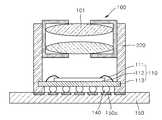
도 3을 참조하면, 본 발명의 일실시예에 따른 카메라 모듈은 하나 이상의 렌즈(101)를 포함하는 렌즈부(100)를 포함한다. 렌즈(101)는 유리 같은 투명한 재질을 구면 또는 비구면으로 만들어 물체로부터 오는 빛을 모으거나, 발산시켜 광학적 상(像)을 맺게 한다. 카메라 모듈의 렌즈(101)는 여러 개로 구성될 수 있으며, 각각의 렌즈(101)들은 경통(미도시) 내에 고정될 수도 있다. 렌즈(101)는 플라스틱 렌즈와 글래스 렌즈가 있는데, 플라스틱 렌즈는 사출 성형에 의한 단위당 생산 비용이 저렴하고 대규모 생산이 가능하여 현재 많이 사용하고 있으며, 글래스 렌즈는 메가(Mega)급의 고해상도를 대응에 유리하나 복잡한 절삭 및 연마공정으로 단가가 높고 구형 혹은 평면 렌즈 이외의 렌즈 구현이 어려운 단점이 있다. 렌즈부(100)의 결합 구성은 카메라 모듈의 특성에 따라 다양한 구조가 가능하므로 본 발명의 실시예들을 도시하는 도면들에서는 생략하여 간단하게 도시하였다. 예를 들어, 렌즈부(100)의 결합 구성은 도 2a 및 도 2b에서 도시된 구성일 수 있으나 본 발명의 일실시예를 구성하는 렌즈부(100)는 이에 한정되지 않는다.Referring to FIG. 3, a camera module according to an embodiment of the present invention includes a
본 발명의 일실시예에 따른 카메라 모듈은 렌즈부(100)를 통과한 광이 결상 되는 이미지 영역을 구비하는 이미지 센서 칩(112)을 포함하는 이미지 센서 패키지(110)를 포함한다. 이미지 센서 칩(112)은 광을 받아들여 전기 신호로 전환하는 소자이다. 동작 및 제작방법에 따라 CCD센서 칩과 CMOS센서 칩으로 분류할 수 있다. CCD(Charge Coupled Device) 센서 칩은 아날로그 회로에 기반을 두고 있으며, 렌즈(101)로 들어온 광이 여러 셀에 뿌려져 각 셀이 그 광에 대한 전하를 저장하고 이 전하의 크기로 명암 정도를 판단한 후, 변환장치로 보내 색상을 표현하는 방식이다. 선명한 화질 표현이 가능하나 데이터 저장용량 및 전력소비량 커, 고화질을 요하는 디지털 카메라 쪽에서 많이 사용한다. CMOS(Complementary Metal Oxide Semi-conductor)센서 칩은 반도체에 아날로그 신호와 디지털 신호처리 회로를 한 곳에 집적시킨 것이다. CCD센서 칩에 대비하여 전력소비가 1/10 정도에 불과하며, 전체적으로 필요한 부분이 한 개의 칩으로 구성되어 있어 보다 소형 제품 제작 가능. 최근 기술수준의 향상으로 이러한 장점 외에 고화질까지 갖춰 디지털 카메라, 카메라폰, PMP(Personal Media Player) 등 여러 분야로 사용처가 많아지고 있다.The camera module according to an embodiment of the present invention includes an
본 발명의 일실시예에서 이미지 센서 패키지(110)는 이미지 센서 칩(112)이 상면에 실장되는 제1 기판(113)을 포함하고, 이미지 센서 칩(112)과 제1 기판(113)을 전기적으로 연결하는 와이어(111)를 포함한다. 본 발명의 일실시예에서 카메라 모듈은 렌즈부(100)와 이미지 센서 패키지(110)의 각각의 측면을 둘러싸는 하우징(120)을 포함한다. 바람직하게는 하우징(120)은 렌즈부(100)의 측면에서 이미지 센서 패키지(110)의 측면까지 신장된다. 하우징(120)은 이미지 센서 패키지(110)를 구성하는 제1 기판(113)의 측면까지 둘러싸는 구조를 가지고 있다. 즉, 이미지 센 서 패키지(110)를 구성하는 제1 기판(113)의 측면이 하우징(120)에 의해 카메라 모듈의 외부에 노출되지 않아서, 이미지 센서 패키지(110)를 전자기파로부터 효과적으로 차폐할 수 있다. 한편, 도 3에서는 하우징(120)은 제1 기판(113)의 상면과 측면에 동시에 접촉하는 구조를 도시하였지만, 본 발명의 변형된 실시예에서는 하우징(120)이 제1 기판(113)의 상면과는 접촉하지 않고 측면만 접촉하는 구조를 가질 수도 있다. 한편, 하우징(120)은 예를 들어, 도전성 페이스트(130)에 의해, 이미지 센서 패키지(110)와 전기적으로 연결될 수 있다. 또한 하우징(120)은 도전성 물질을 포함하는데 적어도 하우징(120)의 외부면은 도전성 물질로 구성되는 것이 바람직하다. 예를 들어, 하우징(120)은 도전성 물질로 형성되는 몸체(Body)로 구성될 수 있다. 상기 도전성 물질은 금속 물질일 수 있으며, 상기 도전성 물질로 형성되는 하우징(120)의 내부면은 절연막이 더 형성될 수 있다. 여기에서 하우징(120)의 내부면이라 함은 렌즈부(100) 및 이미지 센서 패키지(110)과 접촉하면서 둘러싸는 하우징(120)의 내부면을 의미하고, 카메라 모듈의 외부와 접촉하는 하우징(120)의 외부면과 대향하는 면이다. 한편, 하우징(120)은 절연성 물질로 형성되는 몸체와 상기 몸체의 외부면 상에 형성된 도전막으로 구성될 수도 있다. 여기에서, 몸체의 외부면이라 함은 하우징(120)이 카메라 모듈의 외부와 접촉하는 면을 의미하고, 상기 절연성 물질은 액정 고분자(LCP), 폴리카보네이트(polycarbonate) 또는 폴리페닐설파이드(polyphenylsulfide)을 포함할 수 있으며, 상기 도전막은 니켈, 주석, 구리, 금 및 은으로 이루어지는 1군의 원소들 중 적어도 하나 이상의 원소를 함유할 수 있다. 한편, 하우징(120)은 그 내부면에 빛의 난반사를 방지하기 위한 다크 컬러(dark color)의 코팅막이 더 형성될 수 있다.In one embodiment of the present invention, the
도면에는 도시하지 않았지만 본 발명의 일실시예에 따른 카메라 모듈은 적외선 필터를 더 포함할 수 있다. 인간의 가시 범위는 400nm ~ 700nm 이며 이미지 센서가 감지하는 파장은 380nm ~ 1,000nm 이므로 사람의 눈보다 이미지 센서가 적외선에 더 민감하다. 따라서 적외선 필터는 적외선에 더 민감한 이미지 센서에 이미지 정보가 도달하기 전에 적외선 영역을 차단시켜 올바른 색재현성을 구현하기 위해 필요할 수 있다.Although not shown in the drawings, the camera module according to an embodiment of the present invention may further include an infrared filter. The human visible range is 400nm to 700nm and the image sensor detects wavelengths of 380nm to 1,000nm, so the image sensor is more sensitive to infrared light than the human eye. Therefore, an infrared filter may be necessary to block the infrared region before image information arrives at the image sensor, which is more sensitive to infrared rays, to achieve correct color reproduction.
본 발명의 일실시예에 따른 카메라 모듈은 이미지 센서 패키지(110)의 하부에 배치되어 이미지 센서 패키지(110)와 카메라폰, 디지털 카메라, PMP 등의 전자기기의 메인 기판(150)을 전기적으로 연결하는 구조물, 예를 들어 솔더볼(140)을 더 포함할 수 있다.The camera module according to an embodiment of the present invention is disposed under the
솔더볼(140)은 이미지 센서 패키지(110)의 하면에 형성된 도전성의 제1 접지 패드(도 5의 214)와 메인 기판(150) 상면에 형성된 도전성의 제2 접지 패드(150a)를 전기적으로 연결한다. 한편, 메인 기판(150)은 PWB(Printed Wire Board), 플렉시블 PWB(Flexible PWB) 또는 리지드 플렉시블 PWB(Rigid Flexible PWB)일 수 있다. 일반적으로 PWB는 여러 종류의 많은 부품을 페놀수지 또는 에폭시수지로 된 평판 위에 밀집탑재하고 각 부품간을 연결하는 회로를 수지평판의 표면에 밀집 단축하여 고정시킨 회로기판을 말한다. PWB는 페놀수지 절연판 또는 에폭시수지 등의 한쪽면에 구리 등의 박판을 부착시킨 다음 회로의 배선 패턴에 따라 식각(선상의 회로만 남기고 부식시켜 제거)하여 필요한 회로를 구성하고 부품들을 부착 탑재시 키기 위한 구멍을 뚫어 만든다. 배선회로 면의 수에 따라 단면기판, 양면기판, 다층기판 등으로 분류되며 층수가 많을수록 부품의 실장력이 우수, 고정밀제품에 채용된다. 또한 회로기판이 움직여야 하는 경우와 부품의 삽입, 구성시 회로기판의 굴곡을 요하는 경우에 유연성으로 대응할 수 있도록 만든 회로기판을 플렉시블 기판(Flexible PWB)이라고 한다. 한편, 리지드(rigid) 부분과 플렉시블(flexible) 부분이 결합된 리지드 플렉시블 기판(Rigid Flexible PWB)이 이용되기도 한다.The
도 4는 본 발명의 다른 실시예에 따른 카메라 모듈의 단면을 도해하는 단면도이다.4 is a cross-sectional view illustrating a cross section of a camera module according to another embodiment of the present invention.
도 4를 참조하면, 본 발명의 다른 실시예에 따른 카메라 모듈은 하나 이상의 렌즈(101)를 포함하는 렌즈부(100)를 포함한다. 렌즈(101)에 관한 상세한 설명은 도 3에서와 동일하다.Referring to FIG. 4, a camera module according to another embodiment of the present invention includes a
본 발명의 다른 실시예에 따른 카메라 모듈은 렌즈부(100)를 통과한 광이 결상되는 이미지 영역을 구비하는 이미지 센서 칩(212)을 포함하는 이미지 센서 패키지(210)를 포함한다. 이미지 센서 패키지(210)는 이미지 센서 칩(212)을 포함하는 이미지 센서 칩 스케일 패키지(Image Sensor CSP)일 수 있다. 칩 스케일 패키지(또는 칩 사이즈 패키지)는 근간에 개발되어 제안되고 있는 새로운 패키지 유형으로서, 전형적인 플라스틱 패키지에 비하여 많은 장점들을 가지고 있다. 칩 스케일 패키지의 가장 큰 장점은 바로 패키지의 크기이다. JEDEC(Joint Electron Device Engineering Council), EIAJ(Electronic Industry Association of Japan)와 같은 국제 반도체 협회의 정의에 따르면, 칩 스케일 패키지는 일반적으로 칩 크기의 1.2 배 이내의 크기의 패키지에 대한 분류명이다. 칩 스케일 패키지는 디지털 캠코더, 휴대 전화기, 노트북 컴퓨터, 메모리 카드 등과 같이 소형화, 이동성이 요구되는 제품들에 주로 사용되며, DSP(digital signal processor), ASIC(application specific integrated circuit), 마이크로 컨트롤러(micro controller) 등과 같은 반도체 소자들이 칩 스케일 패키지 안에 실장된다. 또한, DRAM(dynamic random access memory), 플래쉬 메모리(flash memory) 등과 같은 메모리 소자를 실장한 칩 스케일 패키지의 사용도 확대되고 있다. 이미지 센서 칩(212)의 상면에는 글래스층(211)이 형성될 수 있다. 이미지 센서 칩(212)은 광을 받아들여 전기 신호로 전환하는 소자이다. 동작 및 제작방법에 따라 CCD센서 칩과 CMOS센서 칩으로 분류할 수 있다.The camera module according to another embodiment of the present invention includes an
본 발명의 다른 실시예에서 카메라 모듈은 렌즈부(100)와 이미지 센서 패키지(210)의 각각의 측면을 둘러싸는 하우징(120)을 포함한다. 바람직하게는 하우징(120)은 렌즈부(100)의 측면에서 이미지 센서 패키지(210)의 측면까지 신장된다. 하우징(120)은 이미지 센서 패키지(210)를 구성하는 이미지 센서 칩(212)의 측면까지 둘러싸는 구조를 가지고 있다. 즉, 이미지 센서 패키지(210)를 구성하는 이미지 센서 칩(212)의 측면이 하우징(120)에 의해 카메라 모듈의 외부에 노출되지 않아서, 이미지 센서 패키지(210)를 전자기파로부터 효과적으로 차폐할 수 있다. 한편, 하우징(120)은 예를 들어, 도전성 페이스트(130)에 의해, 이미지 센서 패키지(210)와 전기적으로 연결될 수 있다. 또한 하우징(120)은 도전성 물질을 포함하는데 적어도 하우징(120)의 외부면은 도전성 물질로 구성되는 것이 바람직하다. 예를 들 어, 하우징(120)은 도전성 물질로 형성되는 몸체(Body)로 구성될 수 있다. 상기 도전성 물질은 금속 물질일 수 있으며, 상기 도전성 물질로 형성되는 하우징(120)의 내부면은 절연막이 더 형성될 수 있다. 여기에서 하우징(120)의 내부면이라 함은 렌즈부(100) 및 이미지 센서 패키지(110)과 접촉하면서 둘러싸는 하우징(120)의 내부면을 의미하고, 카메라 모듈의 외부와 접촉하는 하우징(120)의 외부면과 대향하는 면이다. 한편, 하우징(120)은 절연성 물질로 형성되는 몸체와 상기 몸체의 외부면 상에 형성된 도전막으로 구성될 수도 있다. 여기에서, 몸체의 외부면이라 함은 하우징(120)이 카메라 모듈의 외부와 접하는 면을 의미하고, 상기 절연성 물질은 액정 고분자(LCP), 폴리카보네이트(polycarbonate) 또는 폴리페닐설파이드(polyphenylsulfide)을 포함할 수 있으며, 상기 도전막은 니켈, 주석, 구리, 금 및 은으로 이루어지는 1군의 원소들 중 적어도 하나 이상의 원소를 함유할 수 있다.In another embodiment of the present invention, the camera module includes a
본 발명의 다른 실시예에 따른 카메라 모듈은 이미지 센서 패키지(210)의 하부에 배치되어 이미지 센서 패키지(210)와 카메라폰, 디지털 카메라, PMP등의 전자기기의 메인 기판(150)을 전기적으로 연결하는 구조물, 예를 들어 솔더볼(140)을 더 포함할 수 있다. 솔더볼(140)은 이미지 센서 패키지(210)의 하면에 형성된 도전성의 제1 접지 패드(도 5의 214)와 메인 기판(150) 상면에 형성된 도전성의 제2 접지 패드(150a)를 전기적으로 연결한다. 한편, 메인 기판(150)은 PWB(Printed Wire Board), 플렉시블 PWB(Flexible PWB) 또는 리지드 플렉시블 PWB(Rigid Flexible PWB)일 수 있다.The camera module according to another embodiment of the present invention is disposed under the
도 5는 본 발명의 실시예들에 따른 카메라 모듈에서 도전성 페이스트로 연결된 영역을 확대하여 도해한 단면도이다.5 is an enlarged cross-sectional view illustrating a region connected with a conductive paste in a camera module according to embodiments of the present invention.
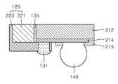
도 5를 참조하면, 하우징과 이미지 센서 패키지를 전기적으로 연결하는 영역을 확대하여 도시하고 있다. 예를 들어, 도 3의 A 영역과 도 4의 B 영역이 확대된 영역이다. 여기에서는 도 4의 B 영역을 참고로 하여 설명하지만 도 3의 A 영역도 동일하게 적용됨은 당연하다. 하우징(120)은 도전성 물질을 포함하여 형성될 수 있는데, 예를 들어 절연성 물질로 형성되는 몸체(221)와 몸체(221)의 외부면에 형성된 도전막(222)을 포함하여 형성될 수 있다. 도전막(222)은 몸체(221)의 측면에서 몸체(221)의 하면까지 신장할 수 있다. 즉, 도전막(222)은 이미지 센서 패키지의 하면까지는 신장하지 않는다. 도 4에서 도시된 이미지 센서 패키지에서는 이미지 센서 패키지의 하면은 이미지 센서 칩(212)의 하면이 된다. 한편, 도 3에서 도시된 이미지 센서 패키지에서는 이미지 센서 패키지의 하면은 제1 기판(113)의 하면이 된다. 이미지 센서 패키지의 하면에는 도전성의 제1 접지 패드(214)가 형성되며, 제1 접지 패드(214)와 하우징(120)은 도전성 페이스트(conductive paste, 130)에 의해 전기적으로 연결된다. 바람직하게는 도전성 페이스트(130)는 솔더 페이스트(solder paste) 또는 은 에폭시(Ag-Epoxy) 수지일 수 있다. 도전성 페이스트(130)는 하우징(120)의 하면에서부터 제1 접지 패드(214)까지 신장하여 형성될 수 있다. 한편, 이미지 센서 패키지의 측면과 하우징(120) 사이의 간극이 형성되는 경우 도전성 페이스트(130)가 상기 간극에 채워지는 것을 방지하기 위하여 상기 간극에는 비도전성 페이스트(135)가 채워질 수 있다. 제1 접지 패드(214)의 하에 형 성된 솔더볼(140)은 이미지 센서 패키지와 메인 기판(도 4의 150)을 전기적으로 연결한다. 이미지 센서 패키지는 그 하면에 PSR 패턴(215)을 더 포함할 수 있다. 도전성 페이스트(130) 및 솔더볼(140)에 의해 도전성 물질을 포함하여 형성되는 하우징(120)과 이미지 센서 패키지 하면의 제1 접지 패드(214)와 메인 기판의 제2 접지 패드(150a)가 전기적으로 접지되어 전자기파를 효과적으로 차폐할 수 있다.Referring to FIG. 5, an enlarged view of an area electrically connecting the housing and the image sensor package is illustrated. For example, region A of FIG. 3 and region B of FIG. 4 are enlarged regions. Here, the description will be made with reference to the region B of FIG. 4, but the region A of FIG. 3 is also applicable. The
도 6은 본 발명의 다른 실시예들에 따른 카메라 모듈에서 도전성 페이스트로 연결된 영역을 확대하여 도해한 단면도이다.6 is an enlarged cross-sectional view illustrating an area connected with a conductive paste in a camera module according to other embodiments of the present invention.
도 6를 참조하면, 하우징과 이미지 센서 패키지를 전기적으로 연결하는 영역을 확대하여 도시하고 있다. 여기에서는 도 4의 B 영역을 참고로 하여 설명하지만 도 3의 A 영역도 동일하게 적용됨은 당연하다. 하우징(120)은 도전성 물질을 포함하여 형성될 수 있는데, 예를 들어 절연성 물질로 형성되는 몸체(221)와 몸체(221)의 외부면에 형성된 도전막(223)을 포함하여 형성될 수 있다. 도전막(223)은 몸체(221)의 측면에서 몸체(221)의 하면을 지나서 이미지 센서 패키지의 하면까지 신장할 수 있다. 도 4에서 도시된 이미지 센서 패키지에서는 이미지 센서 패키지의 하면은 이미지 센서 칩(212)의 하면이 된다. 한편, 도 3에서 도시된 이미지 센서 패키지에서는 이미지 센서 패키지의 하면은 제1 기판(113)의 하면이 된다. 이미지 센서 패키지의 하면에는 도전성의 제1 접지 패드(214)가 형성되며, 신장된 도전막(223)과 제1 접지 패드(214)가 접촉하여 하우징(120)과 전기적으로 연결된다. 제1 접지 패드(214)와 하우징(120)은 도전성 페이스트(131)에 의해 전기적 연결을 강화할 수 있다. 또는 제1 접지 패드(214)의 하면에 형성된 도전막(223)의 일부는 제 1 접지 패드(214)가 노출되도록 비아홀을 형성하고, 도전성 페이스트(131)는 제1 접지 패드(214)를 노출하는 도전막(223)의 비아홀을 채워 전기적 연결을 강화할 수 있다. 바람직하게는 도전성 페이스트(131)는 솔더 페이스트(solder paste) 또는 은 에폭시 수지(Ag-Epoxy)일 수 있다. 상기 비아홀은 식각 및/또는 도금 등 통상적인 제조방법에 의해 형성될 수 있으므로 여기에서는 설명을 생략한다.Referring to FIG. 6, an enlarged area for electrically connecting the housing and the image sensor package is illustrated. Here, the description will be made with reference to the region B of FIG. 4, but the region A of FIG. 3 is also applicable. The
한편, 이미지 센서 패키지의 측면과 하우징(120) 사이의 간극이 형성되는 경우 비도전성 페이스트(135)가 상기 간극을 채울 수 있도록 형성될 수 있다. 제1 접지 패드(214)의 하에 형성된 솔더볼(140)은 이미지 센서 패키지와 메인 기판(도 4의 150)을 전기적으로 연결한다. 이미지 센서 패키지는 그 하면에 PSR 패턴(215)을 더 포함할 수 있다. 도전성 페이스트(131) 및 솔더볼(140)에 의해 도전성 물질을 포함하여 형성되는 하우징(120)과 이미지 센서 패키지 하면의 제1 접지 패드(214)와 메인 기판의 제2 접지 패드(150a)가 전기적으로 접지되어 전자기파를 효과적으로 차폐할 수 있다.Meanwhile, when a gap between the side of the image sensor package and the
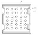
도 7은 도 6에 도시된 도전성 페이스트를 포함하는 카메라 모듈의 하부를 도해하는 하면도이다.FIG. 7 is a bottom view illustrating a lower portion of the camera module including the conductive paste shown in FIG. 6.
도 7을 참조하면, 이미지 센서 패키지의 하면에는 복수개의 솔더볼(140)이 배열되어 있다. 한편, 하우징을 구성하는 도전막(223)과 이미지 센서 패키지를 전기적으로 연결하기 위하여 도전성 페이스트(131)가 도전막(223)의 비아홀을 채워 형성된다. 이미지 센서 패키지(212) 하면의 솔더볼(140) 배선을 방해하지 않으며, 전자기기 메인기판(150)의 배선에 전기적인 영향을 최소화하도록 도전막(223)은 이 미지 센서 패키지의 하면의 일부 영역에서만 형성되는 것이 바람직하다. 도 7에서는 예시적으로 도전성 페이스트(131)가 4개의 영역에서 형성되었다. 도전성 페이스트(131)로 솔더 페이스트를 사용하면 리플로우(reflow) 공정을 사용할 수 있는데, 도전막(223)에 형성된 비아홀은 솔더 페이스트가 여러 방향으로 흐를 가능성을 방지하는 효과도 있다.Referring to FIG. 7, a plurality of
도 8은 본 발명의 또 다른 실시예에 따른 카메라 모듈의 단면을 도해하는 단면도이다.8 is a cross-sectional view illustrating a cross section of a camera module according to another embodiment of the present invention.
도 8을 참조하면, 본 발명의 또 다른 실시예에 따른 카메라 모듈은 하나 이상의 렌즈(101)를 포함하는 렌즈부(100)를 포함한다. 렌즈(101)에 관한 상세한 설명은 도 3에서와 동일하다. 본 발명의 또 다른 실시예에 따른 카메라 모듈은 렌즈부(100)를 통과한 광이 결상되는 이미지 영역을 구비하는 이미지 센서 칩(112) 및 제1 기판(113)을 포함하는 이미지 센서 패키지(110)를 포함한다. 그러나 이미지 센서 패키지는 상기 구성에 한정하지 않으며 도 4에서 도시된 이미지 센서 칩 스케일 패키지(210)일 수 있다.Referring to FIG. 8, a camera module according to another embodiment of the present invention includes a
본 발명의 또 다른 실시예에서 카메라 모듈은 렌즈부(100)와 이미지 센서 패키지(210)의 각각의 측면을 둘러싸는 하우징(220)을 포함한다. 하우징(220)은 렌즈부(100)의 측면에서 이미지 센서 패키지(110)의 측면을 지나서 메인 기판(150)까지 신장할 수 있다. 예를 들어, 메인 기판(150)은 도전성의 제2 접지 패드(150a)를 더 포함할 수 있고 하우징(220)은 제2 접지 패드(150a)까지 신장할 수 있다. 하우징(220)과 제2 접지 패드(150a) 사이에는 솔더 페이스트가 형성되어 전기적 저항을 줄여 접지 효과를 높일 수 있다. 이미지 센서 패키지(110)의 측면 및 하면까지 하우징(220)에 의해 카메라 모듈의 외부에 노출되지 않아서, 이미지 센서 패키지(110)를 전자기파로부터 효과적으로 차폐할 수 있다. 또한 하우징(120)은 도전성 물질을 포함하는데 적어도 하우징(120)의 외부면은 앞에서 설명한 것처럼 도전성 물질로 구성되는 것이 바람직하다.In another embodiment of the present invention, the camera module includes a
도 9는 본 발명의 또 다른 실시예에 따른 카메라 모듈의 단면을 도해하는 단면도이다.9 is a cross-sectional view illustrating a cross section of a camera module according to another embodiment of the present invention.
도 9를 참조하면, 하우징(320)은 이미지 센서 패키지(210)의 측면을 지나서 렌즈부(100)의 측면을 지나 렌즈부(100)의 상면 외곽부까지 신장할 수 있다. 렌즈부(100)의 상면 외곽부라 함은 렌즈(101)에서 광이 통과하지 않는 부위를 의미한다. 하우징(320)의 렌즈부(100)의 상면 외곽부까지 신장하여 형성되므로 전자기파를 더욱 효율적으로 차폐할 수 있게 된다. 하우징(320)과 이미지 센서 패키지의 전기적 연결 구조는 앞에서 설명한 실시예들에서 이미 설명하였다.Referring to FIG. 9, the
발명의 특정 실시예들에 대한 이상의 설명은 예시 및 설명을 목적으로 제공되었다. 따라서, 본 발명은 상기 실시예들에 한정되지 않으며, 본 발명의 기술적 사상 내에서 해당 분야에서 통상의 지식을 가진 자에 의하여 상기 실시예들을 조합하여 실시하는 등 여러 가지 많은 수정 및 변경이 가능함은 명백하다.The foregoing description of specific embodiments of the invention has been presented for purposes of illustration and description. Therefore, the present invention is not limited to the above embodiments, and various modifications and changes are possible in the technical spirit of the present invention by combining the above embodiments by those skilled in the art. It is obvious.
도 1은 카메라 모듈의 단면을 도해하는 단면도이다.1 is a cross-sectional view illustrating a cross section of the camera module.
도 2a는 일반적인 카메라 모듈의 예시적인 분해 사시도이고, 도 2b는 도 2a의 결합 단면도이다.2A is an exemplary exploded perspective view of a general camera module, and FIG. 2B is a combined cross-sectional view of FIG. 2A.
도 3은 본 발명의 일실시예에 따른 카메라 모듈의 단면을 도해하는 단면도이다.3 is a cross-sectional view illustrating a cross section of the camera module according to an embodiment of the present invention.
도 4는 본 발명의 다른 실시예에 따른 카메라 모듈의 단면을 도해하는 단면도이다.4 is a cross-sectional view illustrating a cross section of a camera module according to another embodiment of the present invention.
도 5는 본 발명의 실시예들에 따른 카메라 모듈에서 도전성 페이스트로 연결된 영역을 확대하여 도해한 단면도이다.5 is an enlarged cross-sectional view illustrating a region connected with a conductive paste in a camera module according to embodiments of the present invention.
도 6은 본 발명의 다른 실시예들에 따른 카메라 모듈에서 도전성 페이스트로 연결된 영역을 확대하여 도해한 단면도이다.6 is an enlarged cross-sectional view illustrating an area connected with a conductive paste in a camera module according to other embodiments of the present invention.
도 7은 도 6에 도시된 도전성 페이스트를 포함하는 카메라 모듈의 하부를 도해하는 하면도이다.FIG. 7 is a bottom view illustrating a lower portion of the camera module including the conductive paste shown in FIG. 6.
도 8은 본 발명의 또 다른 실시예에 따른 카메라 모듈의 단면을 도해하는 단면도이다.8 is a cross-sectional view illustrating a cross section of a camera module according to another embodiment of the present invention.
도 9는 본 발명의 또 다른 실시예에 따른 카메라 모듈의 단면을 도해하는 단면도이다.9 is a cross-sectional view illustrating a cross section of a camera module according to another embodiment of the present invention.
<도면의 주요 부분에 대한 부호의 설명><Explanation of symbols for the main parts of the drawings>
100 : 렌즈부100: lens unit
120, 220, 320 : 하우징120, 220, 320: housing
110, 210 : 이미지 센서 패키지110, 210: Image Sensor Package
130 : 도전성 페이스트130: conductive paste
140 : 도전볼150 : 메인 기판140: conductive ball 150: main substrate
Claims (20)
Translated fromKoreanPriority Applications (2)
| Application Number | Priority Date | Filing Date | Title |
|---|---|---|---|
| KR1020070111011AKR100909970B1 (en) | 2007-11-01 | 2007-11-01 | Camera module |
| US12/262,605US8139145B2 (en) | 2007-11-01 | 2008-10-31 | Camera module |
Applications Claiming Priority (1)
| Application Number | Priority Date | Filing Date | Title |
|---|---|---|---|
| KR1020070111011AKR100909970B1 (en) | 2007-11-01 | 2007-11-01 | Camera module |
Publications (2)
| Publication Number | Publication Date |
|---|---|
| KR20090044768A KR20090044768A (en) | 2009-05-07 |
| KR100909970B1true KR100909970B1 (en) | 2009-07-29 |
Family
ID=40587717
Family Applications (1)
| Application Number | Title | Priority Date | Filing Date |
|---|---|---|---|
| KR1020070111011AActiveKR100909970B1 (en) | 2007-11-01 | 2007-11-01 | Camera module |
Country Status (2)
| Country | Link |
|---|---|
| US (1) | US8139145B2 (en) |
| KR (1) | KR100909970B1 (en) |
Families Citing this family (39)
| Publication number | Priority date | Publication date | Assignee | Title |
|---|---|---|---|---|
| CA2685080A1 (en) | 2007-04-24 | 2008-11-06 | Flextronics Ap Llc | Small form factor modules using wafer level optics with bottom cavity and flip-chip assembly |
| US9118825B2 (en)* | 2008-02-22 | 2015-08-25 | Nan Chang O-Film Optoelectronics Technology Ltd. | Attachment of wafer level optics |
| CN101877731B (en)* | 2009-04-30 | 2013-10-09 | 深圳富泰宏精密工业有限公司 | Camera device and portable electronic device with same |
| JP2010283597A (en)* | 2009-06-04 | 2010-12-16 | Toshiba Corp | Semiconductor imaging device |
| US9419032B2 (en)* | 2009-08-14 | 2016-08-16 | Nanchang O-Film Optoelectronics Technology Ltd | Wafer level camera module with molded housing and method of manufacturing |
| KR101712364B1 (en)* | 2010-05-18 | 2017-03-07 | 삼성전자주식회사 | Camera module and method of manufacturing the image sensor module |
| TWI495340B (en)* | 2010-06-10 | 2015-08-01 | Hon Hai Prec Ind Co Ltd | Image sensing module and camera module |
| KR20120016499A (en)* | 2010-08-16 | 2012-02-24 | 삼성전자주식회사 | Camera module |
| DE102010052730B4 (en)* | 2010-11-26 | 2017-01-26 | Conti Temic Microelectronic Gmbh | Optical device for a motor vehicle and method for its production |
| US8251601B2 (en)* | 2010-12-21 | 2012-08-28 | Visera Technologies Company Limited | Camera module and method for fabricating the same |
| CN107889344A (en)* | 2012-08-15 | 2018-04-06 | 深圳迈辽技术转移中心有限公司 | Flexible printed circuit device |
| TWI547161B (en)* | 2012-08-16 | 2016-08-21 | 鴻海精密工業股份有限公司 | Image sensor module and image capturing module |
| DE102012222905A1 (en)* | 2012-12-12 | 2014-06-12 | Robert Bosch Gmbh | Camera arrangement and method for its production |
| KR102142122B1 (en)* | 2012-12-12 | 2020-08-06 | 엘지이노텍 주식회사 | Camera Module |
| KR102041630B1 (en)* | 2013-03-06 | 2019-11-07 | 삼성전기주식회사 | Lens module and manufacturing method for the same |
| US9596748B2 (en)* | 2013-03-28 | 2017-03-14 | Stmicroelectronics Pte Ltd | Lens mount with conductive glue pocket for grounding to a circuit board |
| TW201442508A (en)* | 2013-04-23 | 2014-11-01 | Hon Hai Prec Ind Co Ltd | Camera module |
| CN104284060B (en)* | 2013-07-12 | 2019-07-02 | 鸿富锦精密工业(深圳)有限公司 | camera module |
| KR102256719B1 (en) | 2014-05-12 | 2021-05-28 | 삼성전자주식회사 | semiconductor package and method for manufacturing of the same |
| JP6319026B2 (en)* | 2014-09-29 | 2018-05-09 | 日亜化学工業株式会社 | Light emitting device and manufacturing method thereof |
| WO2016064003A1 (en)* | 2014-10-23 | 2016-04-28 | 하나마이크론(주) | Method for preparing integrated circuit device package |
| JPWO2016084395A1 (en)* | 2014-11-27 | 2017-08-31 | パナソニックIpマネジメント株式会社 | Imaging device |
| US9525832B1 (en) | 2015-06-16 | 2016-12-20 | Stmicroelectronics Pte Ltd | Image sensor device with an electromagnetic compatibility shield (EMC) and associated methods |
| US10666841B2 (en) | 2015-11-11 | 2020-05-26 | Boston Scientific Scimed, Inc. | Visualization device and related systems and methods |
| CN105744127B (en)* | 2015-11-13 | 2020-04-28 | 宁波舜宇光电信息有限公司 | Camera module and electrical support and assembling method thereof |
| US9851478B2 (en) | 2016-02-10 | 2017-12-26 | Microsoft Technology Licensing, Llc | Optical cross talk mitigation for optical device having disrupting features formed on a shield |
| KR102556516B1 (en) | 2016-08-11 | 2023-07-17 | 엘지이노텍 주식회사 | Camera module |
| KR20180046960A (en)* | 2016-10-28 | 2018-05-10 | 삼성디스플레이 주식회사 | Display device |
| KR102635686B1 (en)* | 2016-12-13 | 2024-02-14 | 삼성전자주식회사 | Camera module and electronic device with the same |
| CN106850882B (en)* | 2016-12-20 | 2020-03-24 | Oppo广东移动通信有限公司 | Bracket component and mobile terminal |
| US10926714B2 (en) | 2017-11-10 | 2021-02-23 | Magna Electronics Inc. | Vehicle camera with EMI shielding |
| US10911656B2 (en) | 2017-11-21 | 2021-02-02 | Microsoft Technology Licensing, Llc | Optical isolation systems for displays |
| KR102058865B1 (en)* | 2018-04-12 | 2019-12-24 | (주)아이엠 | Heating device using hyper heat accelerator and method for manufacturing the same |
| JP2020072110A (en)* | 2018-10-29 | 2020-05-07 | ソニーセミコンダクタソリューションズ株式会社 | Imaging device and imaging device |
| KR102622558B1 (en)* | 2019-04-04 | 2024-01-09 | 삼성전자 주식회사 | Electronic device including 3d depth sensor module |
| CN110445971B (en)* | 2019-08-27 | 2025-01-03 | 湖北玥研科技有限公司 | Shockproof aerial camera housing |
| US12320916B1 (en)* | 2021-07-19 | 2025-06-03 | Waymo Llc | Static dome assembly for LiDAR systems |
| US12262103B2 (en) | 2021-10-25 | 2025-03-25 | Magna Electronics Inc. | Vehicular camera with enhanced EMI shielding |
| CN119730431A (en)* | 2025-02-27 | 2025-03-28 | 甬矽半导体(宁波)有限公司 | Image sensor packaging structure and preparation method thereof |
Citations (2)
| Publication number | Priority date | Publication date | Assignee | Title |
|---|---|---|---|---|
| KR20050110901A (en)* | 2004-05-20 | 2005-11-24 | 삼성전자주식회사 | Flip chip package, image sensor module including the package and method of manufacturing the same |
| KR20060091906A (en)* | 2005-02-16 | 2006-08-22 | 삼성전기주식회사 | Camera module |
Family Cites Families (10)
| Publication number | Priority date | Publication date | Assignee | Title |
|---|---|---|---|---|
| JP2003318585A (en)* | 2002-04-24 | 2003-11-07 | Toshiba Corp | Electronics |
| JP2006165624A (en)* | 2004-12-02 | 2006-06-22 | Konica Minolta Opto Inc | Image pickup apparatus and portable terminal having the same |
| KR100593555B1 (en) | 2004-02-26 | 2006-06-28 | (주)아이디에스 | Video camera module |
| KR101091897B1 (en)* | 2004-11-30 | 2011-12-12 | 삼성테크윈 주식회사 | Control apparatus of specific function and camera module comprising the same |
| KR100616670B1 (en)* | 2005-02-01 | 2006-08-28 | 삼성전기주식회사 | Wafer-level image sensor module and its manufacturing method |
| JP2007155800A (en) | 2005-11-30 | 2007-06-21 | Mitsumi Electric Co Ltd | The camera module |
| KR100735380B1 (en) | 2005-12-26 | 2007-07-04 | 삼성전기주식회사 | Camera module |
| KR100748722B1 (en)* | 2006-04-03 | 2007-08-13 | 삼성전자주식회사 | Micro Device Package Module and Manufacturing Method Thereof |
| JP2007288755A (en)* | 2006-04-14 | 2007-11-01 | Optopac Co Ltd | The camera module |
| CN101295848B (en)* | 2007-04-27 | 2010-06-09 | 鸿富锦精密工业(深圳)有限公司 | Electric connector and camera device with the same |
- 2007
- 2007-11-01KRKR1020070111011Apatent/KR100909970B1/enactiveActive
- 2008
- 2008-10-31USUS12/262,605patent/US8139145B2/enactiveActive
Patent Citations (2)
| Publication number | Priority date | Publication date | Assignee | Title |
|---|---|---|---|---|
| KR20050110901A (en)* | 2004-05-20 | 2005-11-24 | 삼성전자주식회사 | Flip chip package, image sensor module including the package and method of manufacturing the same |
| KR20060091906A (en)* | 2005-02-16 | 2006-08-22 | 삼성전기주식회사 | Camera module |
Also Published As
| Publication number | Publication date |
|---|---|
| US20090115891A1 (en) | 2009-05-07 |
| KR20090044768A (en) | 2009-05-07 |
| US8139145B2 (en) | 2012-03-20 |
Similar Documents
| Publication | Publication Date | Title |
|---|---|---|
| KR100909970B1 (en) | Camera module | |
| KR100959922B1 (en) | Camera module and manufacturing method | |
| US8351219B2 (en) | Electronic assembly for an image sensing device | |
| EP1942661B1 (en) | Electronic assembly comprising an image sensor chip and fabrication method thereof | |
| US7829966B2 (en) | Electronic assembly for image sensor device | |
| US20160150133A1 (en) | Electronic device module having an imaging unit | |
| US20110285890A1 (en) | Camera module | |
| US7556504B2 (en) | Camera module and camera module assembly | |
| US11405540B2 (en) | Camera module | |
| KR20110001659A (en) | Camera module | |
| KR100721167B1 (en) | Image sensor module and manufacturing method thereof and camera module using same | |
| KR20110135757A (en) | Image sensor chip and camera module including same | |
| KR20150030904A (en) | Camera module | |
| JP2011123497A (en) | Camera module and method of manufacturing the same | |
| KR20040019650A (en) | Interior type camera module | |
| KR20080079086A (en) | Image sensor module, camera module having same and manufacturing method thereof | |
| CN112770019B (en) | Photosensitive assembly, preparation method thereof and camera module | |
| KR20110000952A (en) | Camera module and manufacturing method | |
| KR20080005733A (en) | Image Sensor Module and Camera Module | |
| KR100730062B1 (en) | Camera module with improved noise characteristics | |
| CN114388545B (en) | Imaging module and electronic equipment | |
| KR20080081726A (en) | Image sensor module and camera module having same | |
| KR20060019680A (en) | Image sensor module and camera module having same | |
| KR101056109B1 (en) | Camera module | |
| JP2004221634A (en) | Optical module, method of manufacturing the same, and electronic device |
Legal Events
| Date | Code | Title | Description |
|---|---|---|---|
| A201 | Request for examination | ||
| PA0109 | Patent application | Patent event code:PA01091R01D Comment text:Patent Application Patent event date:20071101 | |
| PA0201 | Request for examination | ||
| E902 | Notification of reason for refusal | ||
| PE0902 | Notice of grounds for rejection | Comment text:Notification of reason for refusal Patent event date:20090131 Patent event code:PE09021S01D | |
| PG1501 | Laying open of application | ||
| E701 | Decision to grant or registration of patent right | ||
| PE0701 | Decision of registration | Patent event code:PE07011S01D Comment text:Decision to Grant Registration Patent event date:20090522 | |
| GRNT | Written decision to grant | ||
| PR0701 | Registration of establishment | Comment text:Registration of Establishment Patent event date:20090723 Patent event code:PR07011E01D | |
| PR1002 | Payment of registration fee | Payment date:20090724 End annual number:3 Start annual number:1 | |
| PG1601 | Publication of registration | ||
| PR1001 | Payment of annual fee | Payment date:20120706 Start annual number:4 End annual number:4 | |
| FPAY | Annual fee payment | Payment date:20130701 Year of fee payment:5 | |
| PR1001 | Payment of annual fee | Payment date:20130701 Start annual number:5 End annual number:5 | |
| FPAY | Annual fee payment | Payment date:20140630 Year of fee payment:6 | |
| PR1001 | Payment of annual fee | Payment date:20140630 Start annual number:6 End annual number:6 | |
| FPAY | Annual fee payment | Payment date:20150630 Year of fee payment:7 | |
| PR1001 | Payment of annual fee | Payment date:20150630 Start annual number:7 End annual number:7 | |
| FPAY | Annual fee payment | Payment date:20160630 Year of fee payment:8 | |
| PR1001 | Payment of annual fee | Payment date:20160630 Start annual number:8 End annual number:8 | |
| FPAY | Annual fee payment | Payment date:20170630 Year of fee payment:9 | |
| PR1001 | Payment of annual fee | Payment date:20170630 Start annual number:9 End annual number:9 | |
| FPAY | Annual fee payment | Payment date:20180629 Year of fee payment:10 | |
| PR1001 | Payment of annual fee | Payment date:20180629 Start annual number:10 End annual number:10 | |
| PR1001 | Payment of annual fee | Payment date:20200630 Start annual number:12 End annual number:12 | |
| PR1001 | Payment of annual fee | Payment date:20210628 Start annual number:13 End annual number:13 | |
| PR1001 | Payment of annual fee | Payment date:20230621 Start annual number:15 End annual number:15 | |
| PR1001 | Payment of annual fee | Payment date:20240626 Start annual number:16 End annual number:16 |