KR100905566B1 - Carrier member for circuit transfer, coreless printed circuit board using the same, and manufacturing method thereof - Google Patents
Carrier member for circuit transfer, coreless printed circuit board using the same, and manufacturing method thereofDownload PDFInfo
- Publication number
- KR100905566B1 KR100905566B1KR1020070042002AKR20070042002AKR100905566B1KR 100905566 B1KR100905566 B1KR 100905566B1KR 1020070042002 AKR1020070042002 AKR 1020070042002AKR 20070042002 AKR20070042002 AKR 20070042002AKR 100905566 B1KR100905566 B1KR 100905566B1
- Authority
- KR
- South Korea
- Prior art keywords
- layer
- circuit
- carrier
- circuit pattern
- land
- Prior art date
- Legal status (The legal status is an assumption and is not a legal conclusion. Google has not performed a legal analysis and makes no representation as to the accuracy of the status listed.)
- Expired - Fee Related
Links
Images


Classifications
- H—ELECTRICITY
- H05—ELECTRIC TECHNIQUES NOT OTHERWISE PROVIDED FOR
- H05K—PRINTED CIRCUITS; CASINGS OR CONSTRUCTIONAL DETAILS OF ELECTRIC APPARATUS; MANUFACTURE OF ASSEMBLAGES OF ELECTRICAL COMPONENTS
- H05K3/00—Apparatus or processes for manufacturing printed circuits
- H—ELECTRICITY
- H05—ELECTRIC TECHNIQUES NOT OTHERWISE PROVIDED FOR
- H05K—PRINTED CIRCUITS; CASINGS OR CONSTRUCTIONAL DETAILS OF ELECTRIC APPARATUS; MANUFACTURE OF ASSEMBLAGES OF ELECTRICAL COMPONENTS
- H05K3/00—Apparatus or processes for manufacturing printed circuits
- H05K3/40—Forming printed elements for providing electric connections to or between printed circuits
- H05K3/42—Plated through-holes or plated via connections
- H05K3/425—Plated through-holes or plated via connections characterised by the sequence of steps for plating the through-holes or via connections in relation to the conductive pattern
- H05K3/428—Plated through-holes or plated via connections characterised by the sequence of steps for plating the through-holes or via connections in relation to the conductive pattern initial plating of through-holes in substrates having a metal pattern
- H—ELECTRICITY
- H05—ELECTRIC TECHNIQUES NOT OTHERWISE PROVIDED FOR
- H05K—PRINTED CIRCUITS; CASINGS OR CONSTRUCTIONAL DETAILS OF ELECTRIC APPARATUS; MANUFACTURE OF ASSEMBLAGES OF ELECTRICAL COMPONENTS
- H05K3/00—Apparatus or processes for manufacturing printed circuits
- H05K3/10—Apparatus or processes for manufacturing printed circuits in which conductive material is applied to the insulating support in such a manner as to form the desired conductive pattern
- H05K3/20—Apparatus or processes for manufacturing printed circuits in which conductive material is applied to the insulating support in such a manner as to form the desired conductive pattern by affixing prefabricated conductor pattern
- H05K3/205—Apparatus or processes for manufacturing printed circuits in which conductive material is applied to the insulating support in such a manner as to form the desired conductive pattern by affixing prefabricated conductor pattern using a pattern electroplated or electroformed on a metallic carrier
- H—ELECTRICITY
- H05—ELECTRIC TECHNIQUES NOT OTHERWISE PROVIDED FOR
- H05K—PRINTED CIRCUITS; CASINGS OR CONSTRUCTIONAL DETAILS OF ELECTRIC APPARATUS; MANUFACTURE OF ASSEMBLAGES OF ELECTRICAL COMPONENTS
- H05K3/00—Apparatus or processes for manufacturing printed circuits
- H05K3/46—Manufacturing multilayer circuits
- H05K3/4602—Manufacturing multilayer circuits characterized by a special circuit board as base or central core whereon additional circuit layers are built or additional circuit boards are laminated
- H—ELECTRICITY
- H05—ELECTRIC TECHNIQUES NOT OTHERWISE PROVIDED FOR
- H05K—PRINTED CIRCUITS; CASINGS OR CONSTRUCTIONAL DETAILS OF ELECTRIC APPARATUS; MANUFACTURE OF ASSEMBLAGES OF ELECTRICAL COMPONENTS
- H05K3/00—Apparatus or processes for manufacturing printed circuits
- H05K3/46—Manufacturing multilayer circuits
- H05K3/4644—Manufacturing multilayer circuits by building the multilayer layer by layer, i.e. build-up multilayer circuits
- H05K3/4652—Adding a circuit layer by laminating a metal foil or a preformed metal foil pattern
- H05K3/4658—Adding a circuit layer by laminating a metal foil or a preformed metal foil pattern characterized by laminating a prefabricated metal foil pattern, e.g. by transfer
- H—ELECTRICITY
- H05—ELECTRIC TECHNIQUES NOT OTHERWISE PROVIDED FOR
- H05K—PRINTED CIRCUITS; CASINGS OR CONSTRUCTIONAL DETAILS OF ELECTRIC APPARATUS; MANUFACTURE OF ASSEMBLAGES OF ELECTRICAL COMPONENTS
- H05K2201/00—Indexing scheme relating to printed circuits covered by H05K1/00
- H05K2201/03—Conductive materials
- H05K2201/0332—Structure of the conductor
- H05K2201/0388—Other aspects of conductors
- H05K2201/0394—Conductor crossing over a hole in the substrate or a gap between two separate substrate parts
- H—ELECTRICITY
- H05—ELECTRIC TECHNIQUES NOT OTHERWISE PROVIDED FOR
- H05K—PRINTED CIRCUITS; CASINGS OR CONSTRUCTIONAL DETAILS OF ELECTRIC APPARATUS; MANUFACTURE OF ASSEMBLAGES OF ELECTRICAL COMPONENTS
- H05K2201/00—Indexing scheme relating to printed circuits covered by H05K1/00
- H05K2201/09—Shape and layout
- H05K2201/09209—Shape and layout details of conductors
- H05K2201/095—Conductive through-holes or vias
- H05K2201/09563—Metal filled via
- H—ELECTRICITY
- H05—ELECTRIC TECHNIQUES NOT OTHERWISE PROVIDED FOR
- H05K—PRINTED CIRCUITS; CASINGS OR CONSTRUCTIONAL DETAILS OF ELECTRIC APPARATUS; MANUFACTURE OF ASSEMBLAGES OF ELECTRICAL COMPONENTS
- H05K2203/00—Indexing scheme relating to apparatus or processes for manufacturing printed circuits covered by H05K3/00
- H05K2203/15—Position of the PCB during processing
- H05K2203/1536—Temporarily stacked PCBs
- H—ELECTRICITY
- H05—ELECTRIC TECHNIQUES NOT OTHERWISE PROVIDED FOR
- H05K—PRINTED CIRCUITS; CASINGS OR CONSTRUCTIONAL DETAILS OF ELECTRIC APPARATUS; MANUFACTURE OF ASSEMBLAGES OF ELECTRICAL COMPONENTS
- H05K3/00—Apparatus or processes for manufacturing printed circuits
- H05K3/38—Improvement of the adhesion between the insulating substrate and the metal
- H05K3/382—Improvement of the adhesion between the insulating substrate and the metal by special treatment of the metal
- H05K3/383—Improvement of the adhesion between the insulating substrate and the metal by special treatment of the metal by microetching
- H—ELECTRICITY
- H05—ELECTRIC TECHNIQUES NOT OTHERWISE PROVIDED FOR
- H05K—PRINTED CIRCUITS; CASINGS OR CONSTRUCTIONAL DETAILS OF ELECTRIC APPARATUS; MANUFACTURE OF ASSEMBLAGES OF ELECTRICAL COMPONENTS
- H05K3/00—Apparatus or processes for manufacturing printed circuits
- H05K3/38—Improvement of the adhesion between the insulating substrate and the metal
- H05K3/382—Improvement of the adhesion between the insulating substrate and the metal by special treatment of the metal
- H05K3/384—Improvement of the adhesion between the insulating substrate and the metal by special treatment of the metal by plating
- Y—GENERAL TAGGING OF NEW TECHNOLOGICAL DEVELOPMENTS; GENERAL TAGGING OF CROSS-SECTIONAL TECHNOLOGIES SPANNING OVER SEVERAL SECTIONS OF THE IPC; TECHNICAL SUBJECTS COVERED BY FORMER USPC CROSS-REFERENCE ART COLLECTIONS [XRACs] AND DIGESTS
- Y10—TECHNICAL SUBJECTS COVERED BY FORMER USPC
- Y10T—TECHNICAL SUBJECTS COVERED BY FORMER US CLASSIFICATION
- Y10T29/00—Metal working
- Y10T29/49—Method of mechanical manufacture
- Y10T29/49002—Electrical device making
- Y10T29/49117—Conductor or circuit manufacturing
- Y10T29/49124—On flat or curved insulated base, e.g., printed circuit, etc.
- Y10T29/49155—Manufacturing circuit on or in base
Landscapes
- Engineering & Computer Science (AREA)
- Manufacturing & Machinery (AREA)
- Microelectronics & Electronic Packaging (AREA)
- Production Of Multi-Layered Print Wiring Board (AREA)
- Manufacturing Of Printed Wiring (AREA)
Abstract
Translated fromKoreanDescription
Translated fromKorean도 1은 본 발명의 바람직한 일 실시형태에 따른 코어리스 인쇄회로기판의 구조를 개략적으로 나타낸 단면도이다.1 is a cross-sectional view schematically showing the structure of a coreless printed circuit board according to a preferred embodiment of the present invention.
도 2a 내지 도 2b는 본 발명의 바람직한 일 실시형태에 따른 다층 코어리스 인쇄회로기판의 구조를 개략적으로 나타낸 단면도이다.2A to 2B are cross-sectional views schematically showing the structure of a multilayer coreless printed circuit board according to a preferred embodiment of the present invention.
도 3a 내지 도 3e는 본 발명의 바람직한 일 실시형태에 따른 회로 전사용 캐리어 부재의 제조공정흐름을 설명하기 위한 도면이다.3A to 3E are diagrams for explaining the manufacturing process flow of the carrier member for circuit transfer according to the preferred embodiment of the present invention.
도 4a 내지 도 4g는 본 발명의 바람직한 일 실시형태에 따른 코어리스 인쇄회로기판의 제조공정흐름을 설명하기 위한 도면이다.4A to 4G are diagrams for explaining a manufacturing process flow of a coreless printed circuit board according to an exemplary embodiment of the present invention.
도 5a 내지 도 5d는 종래기술의 일 실시형태에 따른 인쇄회로기판의 제조공정흐름을 설명하기 위한 도면이다.5A to 5D are diagrams for describing a manufacturing process flow of a printed circuit board according to an exemplary embodiment of the prior art.
도 6은 종래기술의 일 실시형태에 따라 제작된 인쇄회로기판의 회로 형상을 설명하기 위한 도면이다.6 is a view for explaining a circuit shape of a printed circuit board manufactured according to an embodiment of the prior art.
※ 도면의 주요 부분에 대한 부호의 설명 ※※ Explanation of code about main part of drawing ※
100 : 코어리스 인쇄회로기판100: coreless printed circuit board
101, 201, 211 : 수지 절연층102, 104, 202, 212 : 회로 패턴101, 201, 211:
103, 105, 203, 213 : 랜드106, 206, 216 : 비아홀103, 105, 203, 213:
300 : 캐리어 원판300: carrier disc
301 : 접착체302 : 캐리어층301: adhesive 302: carrier layer
303 : 베리어층304 : 도금레지스트303: barrier layer 304: plating resist
305, 306, 307, 308 : 회로 형성 부위305, 306, 307, 308: circuit formation site
309, 311 : 회로 패턴309, 311: circuit pattern
310, 312 : 랜드313 : 요철310, 312: Land 313: Unevenness
C1, C2 : 회로 전사용 캐리어 부재C1, C2: carrier member for circuit transfer
400a, 400b : 회로 전사용 캐리어 부재400a, 400b: carrier member for circuit transfer
401a, 401b : 캐리어층402a, 402b : 베리어층401a, 401b:
403a, 403b : 회로 패턴404a, 404b : 랜드403a, 403b:
405 : 수지 절연층406 : 블라인드 비아홀405: resin insulating layer 406: blind via hole
407a, 407b : 구리 시드층408 : 충전 도금층407a and 407b
본 발명은 회로 전사용 캐리어 부재, 이를 이용한 코어리스 인쇄회로기판, 및 이들의 제조방법에 관한 것이다. 좀 더 구체적으로는, 본 발명은 매립된 회로 패턴을 갖는 코어리스 기판 구조로서 회로 패턴의 내측 하단에만 요철이 형성되도록 구성함으로써 고밀도, 고신뢰도의 인쇄회로기판을 제공할 수 있는 회로 전사용 캐리어 부재, 이를 이용한 코어리스 인쇄회로기판, 및 이들의 제조방법에 관한 것이다.The present invention relates to a carrier member for circuit transfer, a coreless printed circuit board using the same, and a method of manufacturing the same. More specifically, the present invention is a coreless substrate structure having a buried circuit pattern, so that irregularities are formed only on the inner lower end of the circuit pattern, so that a carrier member for circuit transfer capable of providing a high density, high reliability printed circuit board is provided. The present invention relates to a coreless printed circuit board using the same, and a method of manufacturing the same.
현재 기술에서 패키지용 기판으로서 고밀도의 기술이 적용되는 기판으로는 FCBGA 기판을 들 수 있는데, 이들의 대부분이 CPU용, 칩셋용으로 사용되고 있다. 모바일 기기의 적용이 증가함에 따라서 적용되는 패키지 또한 CPU용, 칩셋용을 탑재하고자 하는 요구가 증대되고 있다.In the current technology, a substrate to which high-density technology is applied as a package substrate is an FCBGA substrate, most of which are used for a CPU and a chipset. As the application of mobile devices increases, the applied package also increases the demand for mounting a CPU and a chipset.
이러한 요구를 수용하기 위해서 패키지용 기판의 밀도가 기존보다 훨씬 고밀도가 되어야 하며, 기판의 사이즈 및 두께가 얇아져야 하는 기술적 문제가 발생하게 되었다.In order to accommodate these demands, the density of the substrate for a package must be much higher than that of the conventional, and a technical problem arises that the size and thickness of the substrate must be thinner.
이와 관련하여, 도 5a 내지 도 5d에 종래의 세미에디티브 공법을 통해서 인쇄회로기판을 빌드업하는 과정을 나타내었는 바, 이하 이를 참조하여 설명한다.In this regard, a process of building up a printed circuit board through a conventional semi-additive process is shown in FIGS. 5A to 5D, which will be described with reference to the following.
우선, 서브트렉티브 공법(Subtractive Process), MSAP(Modified Semi Additive Process)와 같은 통상의 코어 회로층 형성 방법에 따라 제1의 수지 절연층(501), 예를 들어, 유리섬유가 함침된 FR-4 수지 기판의 양면에 형성된 내층 회로(502)를 도통홀(503)을 통해서 전기적으로 접속한다. 이어서, 외층 회로 형성을 위하여, 제2의 수지 절연층(504), 예를 들어, 유리섬유가 함침되지 않은 ABF 수지 기판을 적층하고 블라인드 비아홀(505)을 가공한 후, 무전해 도금을 통해서 구리 시드층(506)을 형성한다(도 5a 참조). 블라인드 비아홀(505)을 포함하여 외층 회로가 형성될 위치를 제외한 소정의 위치에 드라이 필름(507)을 도포한 후(도 5b 참조), 이를 도금레지스트로 하여 전해 도금을 통해서 패턴 동도금층(508)을 형성한다(도 5c 참조). 다음, 드라이 필름(507)을 제거하고 플레시 에칭을 통해서 불필요한 부분의 구리 시드층(506)을 제거하여 외층 회로를 완성한다(도 5d 참조).First, FR- impregnated with a first
도 6에 이와 같은 종래의 공정을 통해서 제작되는 인쇄회로기판의 회로 형상을 개략적으로 나타내었다.6 schematically illustrates a circuit shape of a printed circuit board manufactured through such a conventional process.
도 6을 참조하면, 수지 절연층(601, 603) 상에 회로 패턴(602, 604)이 각각 형성되어 있으며, 비아(605)와 회로(604)가 도금과정을 통해서 동시에 구현된다. 이때, 수지 절연층(601, 603)과의 접착력을 높이기 위하여 통상 회로 패턴(602, 604)의 표면에 조도를 부여한다. 그러나, 오른쪽 도면에서 나타낸 바와 같이, 통상적으로 수지 절연층(611) 상에 형성된 구리 시드층(612)을 제거하기 위한 플레시 에칭 시 구리 시드층(612)과 함께 전해 도금층(613)까지도 소정 부분 에칭되어 회로 크기의 손상이 야기될 뿐 아니라(D1), 회로 아랫부분이 과에칭되어(D2) 면적감소로 인하여 미세 회로에서 회로 단락 등, 신뢰성이 떨어지는 단점이 있다.Referring to FIG. 6,
이에 본 발명에서는 상기와 같은 문제점을 해결하기 위하여 광범위한 연구를 거듭한 결과, 외측 상단에만 요철이 형성된 회로 패턴을 갖도록 제작된 회로 전사용 캐리어 부재를 이용하여 회로 패턴을 수지 절연층에 전사하여 매립함으로써 고 밀도, 고신뢰도의 코어리스 인쇄회로기판을 제작할 수 있었고, 본 발명은 이에 기초하여 완성되었다.Accordingly, in the present invention, as a result of extensive research to solve the above problems, by transferring the circuit pattern to the resin insulating layer by embedding the circuit pattern using a carrier member for circuit transfer manufactured to have a circuit pattern with irregularities formed only on the outer top. High density, high reliability coreless printed circuit boards could be fabricated, and the present invention has been completed based on this.
본 발명의 제1측면은 회로의 손상 없이 특정 면에만 요철을 갖는 회로 패턴을 수지 절연층 내에 전사하여 매립하기 위한 회로 전사용 캐리어 부재를 제공하는 것이다.A first aspect of the present invention is to provide a carrier member for circuit transfer for transferring and embedding a circuit pattern having irregularities only in a specific surface without damaging the circuit in the resin insulating layer.
본 발명의 제2측면은 상기 회로 전사용 캐리어 부재의 제조방법을 제공하는 것이다.A second aspect of the present invention is to provide a method of manufacturing the carrier member for circuit transfer.
본 발명의 제3측면은 수지 절연층 내에 매립된 회로 패턴을 갖는 코어리스 인쇄회로기판을 제공하는 것이다.A third aspect of the present invention is to provide a coreless printed circuit board having a circuit pattern embedded in a resin insulating layer.
본 발명의 제4측면은 상기 회로 전사용 캐리어 부재를 이용하여 상기 코어리스 인쇄회로기판을 제조하는 방법을 제공하는 것이다.A fourth aspect of the present invention is to provide a method for manufacturing the coreless printed circuit board using the carrier member for circuit transfer.
본 발명의 바람직한 일 실시형태에 따른 회로 전사용 캐리어 부재의 제조방법은:According to one preferred embodiment of the present invention, a method of manufacturing a carrier member for circuit transfer includes:
(a) 열처리 시 비접착성을 나타내는 열접착제의 양면에 캐리어층 및 베리어층으로 구성된 캐리어 원판이 부착된 양면 캐리어 구조물을 준비하는 단계, 여기서 상기 베리어층은 구리 이외의 금속 시드층임;(a) preparing a double-sided carrier structure having a carrier disc composed of a carrier layer and a barrier layer on both sides of a thermal adhesive that exhibits non-adhesion upon heat treatment, wherein the barrier layer is a metal seed layer other than copper;
(b) 상기 양면 캐리어 구조물의 베리어층 상에, 랜드를 포함하거나 포함하지 않는 회로 형성 부위를 제외한 부분에 도금레지스트를 도포하는 단계;(b) applying a plating resist on the barrier layer of the double-sided carrier structure, except for circuit forming portions including or not including lands;
(c) 상기 도금레지스트를 통해서 오픈된 회로 형성 부위에 전해 동도금을 수행하여 회로 패턴을 형성하는 단계;(c) forming a circuit pattern by performing electrolytic copper plating on the open circuit formation site through the plating resist;
(d) 상기 회로 패턴의 노출된 표면을 조도처리하여 요철을 형성하는 단계; 및(d) roughening the exposed surface of the circuit pattern to form irregularities; And
(e) 상기 도금레지스트를 제거하고, 상기 양면 캐리어 구조물을 열처리하여 열접착제로부터 한 쌍의 회로 전사용 캐리어 부재를 분리하여 얻는 단계;(e) removing the plating resist, and heat treating the double-sided carrier structure to separate a pair of circuit transfer carrier members from a thermal adhesive;
를 포함하는 것을 특징으로 한다.Characterized in that it comprises a.
상기 방법에서, 상기 캐리어층은 바람직하게는 금속 또는 중합체로 이루어진다.In the method, the carrier layer is preferably made of metal or polymer.
상기 양면 캐리어 구조물의 열처리는 바람직하게는 100∼150℃의 온도에서 수행된다.The heat treatment of the double-sided carrier structure is preferably carried out at a temperature of 100 to 150 ℃.
한편, 상기 회로 패턴 폭의 편차는 ±10% 이내인 것이 바람직하다.On the other hand, it is preferable that the deviation of the circuit pattern width is within ± 10%.
바람직하게는, 상기 회로 형성 부위는; 상기 한 쌍의 회로 전사용 캐리어 부재 중 제1의 회로 전사용 캐리어 부재에 형성된 제1층 랜드가 비아홀 가공 부위를 사이에 두고 이격되어 형성되며, 제2의 회로 전사용 캐리어 부재에 형성된 제2층 랜드가 이격 부분 없이 일체로 상기 제1층 랜드에 대향되어 형성되도록 선택된다.Preferably, the circuit formation site; The first layer land formed in the first circuit transfer carrier member of the pair of circuit transfer carrier members is formed to be spaced apart from each other via a via hole processing portion, and the second layer formed in the second circuit transfer carrier member. The lands are selected such that they are formed integrally opposite the first layer lands without spacing.
본 발명의 바람직한 일 실시형태에 따른 회로 전사용 캐리어 부재는:A carrier member for a circuit transfer according to a preferred embodiment of the present invention is:
캐리어층의 일면에 구리 이외의 금속 시드층으로 된 베리어층, 및 랜드를 포함하거나 포함하지 않는 회로 패턴을 가지되, 상기 랜드를 포함하거나 포함하지 않는 회로 패턴의 내측 하단 및 노출된 표면 중 측면에는 요철이 형성되어 있지 않고 외측 상단에만 요철이 형성되어 있는 것을 특징으로 한다.One side of the carrier layer has a barrier layer of a metal seed layer other than copper, and a circuit pattern with or without lands, the inner bottom and exposed surfaces of the circuit pattern with or without lands It is characterized by the fact that the unevenness is not formed but only the outer upper end.
본 발명의 바람직한 일 실시형태에 따른 코어리스 인쇄회로기판의 제조방법은:A method for manufacturing a coreless printed circuit board according to one preferred embodiment of the present invention is:
(a) 캐리어층의 일면에 구리 이외의 금속 시드층으로 된 베리어층, 및 랜드를 포함하는 회로 패턴을 가지되, 상기 랜드를 포함하는 회로 패턴의 내측 하단 및 노출된 표면 중 측면에는 요철이 형성되어 있지 않고 외측 상단에만 요철이 형성되어 있는, 한 쌍의 회로 전사용 캐리어 부재를 준비하는 단계;(a) a barrier layer of a metal seed layer other than copper, and a circuit pattern including lands on one surface of the carrier layer, wherein irregularities are formed on an inner lower side and an exposed surface of the circuit pattern including the lands; Preparing a pair of carrier members for circuit transfer, in which unevenness is formed only on the outer upper end thereof;
(b) 수지 절연층을 준비하는 단계;(b) preparing a resin insulating layer;
(c) 상기 한 쌍의 회로 전사용 캐리어 부재를 회로 패턴이 내층으로 향하도록 서로 대향시켜 상기 수지 절연층에 회로 패턴을 각각 매립하는 단계;(c) filling the circuit pattern in the resin insulating layer by opposing the pair of circuit transfer carrier members so that the circuit pattern faces the inner layer;
(d) 상기 회로 전사용 캐리어 부재의 캐리어층을 제거하여 베리어층을 노출시키는 단계;(d) removing the carrier layer of the carrier member for circuit transfer to expose the barrier layer;
(e) 층간 전기적 접속을 위한 비아홀을 가공하여 랜드의 접촉면을 노출시키는 단계;(e) processing via holes for interlayer electrical connection to expose the contact surface of the land;
(f) 상기 비아홀 내부를 포함하여 베리어층 상에 구리 시드층을 형성하는 단계;(f) forming a copper seed layer on the barrier layer including the inside of the via hole;
(g) 상기 비아홀 내부를 충전 도금하는 단계;(g) charge plating the inside of the via hole;
(h) 상기 구리 시드층을 포함하는 표면층을 에칭하여 베리어층을 노출시키는 단계; 및(h) etching the surface layer comprising the copper seed layer to expose the barrier layer; And
(i) 상기 베리어층을 포함하는 표면층을 에칭하여 회로 패턴을 노출시키는 단계;(i) etching the surface layer including the barrier layer to expose a circuit pattern;
를 포함하는 것을 특징으로 한다.Characterized in that it comprises a.
상기 방법에서, 상기 (c) 단계 내지 (i) 단계는 시트 타입(sheet type)의 공정으로 수행될 수 있다.In the above method, steps (c) to (i) may be performed by a sheet type process.
상기 수지 절연층은 바람직하게는 보강재가 함침되거나 함침되지 않은 열경화성 수지로 이루어질 수 있다.The resin insulating layer may be preferably made of a thermosetting resin impregnated or not impregnated with a reinforcing material.
상기 캐리어층의 제거는 바람직하게는 박리(peeling) 또는 에칭을 통해서 수행될 수 있다.Removal of the carrier layer may preferably be carried out through peeling or etching.
상기 구리 시드층 형성은 무전해 동도금을 통해서 수행되는 것이 바람직하다.The copper seed layer formation is preferably carried out through electroless copper plating.
한편, 상기 한 쌍의 회로 전사용 캐리어 부재 중 제1의 회로 전사용 캐리어 부재에 형성된 제1층 랜드는 비아홀과 양 측면에서 접촉면을 갖도록 비아홀 가공 부위를 사이에 두고 이격되어 형성되며, 제2의 회로 전사용 캐리어 부재에 형성된 제2층 랜드는 내측 상단에서 비아홀과 접촉면을 갖도록 이격 부분 없이 일체로 상기 제1층 랜드에 대향되어 형성되는 것이 바람직하다.Meanwhile, the first layer lands formed in the first circuit transfer carrier member of the pair of circuit transfer carrier members are spaced apart from each other via the via hole processing portion so as to have contact surfaces on both sides thereof. The second layer land formed in the carrier member for circuit transfer is preferably formed to face the first layer land integrally without a spaced portion so as to have a contact surface with a via hole at an inner upper end thereof.
이때, 상기 비아홀 가공은 비아를 형성할 부위의 베리어층을 제거하여 수지 절연층을 노출시킨 후, 수지 절연층을 가공하여 랜드의 접촉면을 노출시켜 수행될 수 있다.In this case, the via hole processing may be performed by exposing the resin insulating layer by removing the barrier layer of the portion where the via is to be formed, and then processing the resin insulating layer to expose the contact surface of the land.
상기 방법은 또한:The method also:
(a') 제2의 캐리어층의 일면에 제2의 베리어층, 및 제2의 랜드를 포함하거나 포함하지 않는 제2의 회로 패턴을 가지되, 상기 제2의 랜드를 포함하거나 포함하지 않는 제2의 회로 패턴의 내측 하단 및 노출된 표면 중 측면에는 요철이 형성되어 있지 않고 외측 상단에만 요철이 형성되어 있는 제2의 회로 전사용 캐리어 부재를 준비하는 단계;(a ') a second barrier layer on one surface of the second carrier layer, and a second circuit pattern including or not including a second land, but including or not including the second land; Preparing a second circuit transfer carrier member having unevenness formed only at the outer upper end of the circuit pattern of FIG.
(b') 상기 코어리스 인쇄회로기판의 단면 또는 양면에 제2의 수지 절연층을 적층하는 단계;(b ') stacking a second resin insulating layer on one or both surfaces of the coreless printed circuit board;
(c') 상기 제2의 회로 전사용 캐리어 부재를 제2의 회로 패턴이 내층으로 향하도록 하여 상기 제2의 수지 절연층에 제2의 회로 패턴을 매립하는 단계;(c ') embedding a second circuit pattern in the second resin insulating layer with the second circuit pattern carrier member facing the inner layer;
(d') 상기 제2의 회로 전사용 캐리어 부재의 제2의 캐리어층을 제거하여 제2의 베리어층을 노출시키는 단계;(d ') exposing the second barrier layer by removing the second carrier layer of the second circuit transfer carrier member;
(e') 층간 전기적 접속을 위한 제2의 비아홀을 가공하되, 제2의 랜드가 존재하는 경우에는 비아홀 가공을 통해서 제2의 랜드의 접촉면을 노출시키는 단계;(e ') processing a second via hole for electrical connection between layers, and if a second land exists, exposing a contact surface of the second land through via hole processing;
(f') 상기 제2의 비아홀 내부를 포함하여 제2의 베리어층 상에 제2의 구리 시드층을 형성하는 단계;(f ') forming a second copper seed layer on the second barrier layer, including inside the second via hole;
(g') 상기 제2의 비아홀 내부를 충전 도금하는 단계;(g ') filling plating the inside of the second via hole;
(h') 상기 제2의 구리 시드층을 포함하는 표면층을 에칭하여 제2의 베리어층을 노출시키는 단계; 및(h ') etching the surface layer comprising the second copper seed layer to expose a second barrier layer; And
(i') 상기 제2의 베리어층을 포함하는 표면층을 에칭하여 제2의 회로 패턴을 노출시키는 단계;(i ') etching the surface layer including the second barrier layer to expose a second circuit pattern;
를 순차적으로 1회 이상 반복하여 인쇄회로기판의 단면 또는 양면에 외층 회 로층을 더욱 형성할 수 있다.By sequentially repeating one or more times, the outer circuit layer may be further formed on one or both sides of the printed circuit board.
본 발명의 바람직한 일 실시형태에 따른 코어리스 인쇄회로기판은:A coreless printed circuit board according to one preferred embodiment of the present invention is:
(a) 수지 절연층;(a) a resin insulating layer;
(b) 상기 수지 절연층의 양면에 각각 표면이 노출되어 매립된, 랜드를 포함하는 회로 패턴; 및(b) a circuit pattern including lands, each of which has a surface exposed and embedded on both surfaces of the resin insulating layer; And
(c) 층간 전기적 접속을 위하여 각 층의 랜드와 접촉하도록 형성된 비아;(c) vias formed in contact with lands in each layer for interlayer electrical connection;
를 포함하며,Including;
상기 랜드를 포함하는 회로 패턴의 노출된 표면 및 매립된 면 중 측면에는 요철이 형성되어 있지 않고 내측 하단에만 요철이 형성되어 있으며, 상기 회로 패턴과 상기 비아는 그 층 구성이 서로 다른 것을 특징으로 한다.The uneven surface is not formed on the side of the exposed surface and the buried surface of the circuit pattern including the land, and the uneven surface is formed only at the inner bottom, and the circuit pattern and the via have different layer configurations. .
여기서, 상기 랜드를 포함하는 회로 패턴은 전해 동도금층으로 이루어지며, 상기 비아는 내측 표면에 형성된 무전해 동박 시드층과 상기 무전해 동박 시드층에 형성된 충전 도금층으로 이루어지는 것이 바람직하다.Here, the circuit pattern including the land is made of an electrolytic copper plating layer, and the via is preferably made of an electroless copper foil seed layer formed on an inner surface and a charge plating layer formed on the electroless copper foil seed layer.
상기 코어리스 인쇄회로기판은 또한:The coreless printed circuit board also includes:
(a') 상기 코어리스 인쇄회로기판의 단면 또는 양면에 적층된 제2의 수지 절연층;(a ') a second resin insulating layer laminated on one or both surfaces of the coreless printed circuit board;
(b') 상기 제2의 수지 절연층에 표면이 노출되어 매립된, 제2의 랜드를 포함하거나 포함하지 않는 제2의 회로 패턴; 및(b ') a second circuit pattern, with or without a second land, having a surface exposed and buried in the second resin insulating layer; And
(c') 층간 전기적 접속을 위하여 형성된 제2의 비아, 단, 제2의 랜드가 존재하는 경우에는 상기 제2의 비아가 제2의 랜드와 접촉하도록 형성됨;(c ') a second via formed for interlayer electrical connection, provided that the second via is in contact with the second land if a second land is present;
을 더욱 포함할 수 있으며,May further include
여기서, 상기 제2의 랜드를 포함하거나 포함하지 않는 제2의 회로 패턴의 노출된 표면 및 매립된 면 중 측면에는 요철이 형성되어 있지 않고 내측 하단에만 요철이 형성되어 있으며, 상기 제2의 회로 패턴과 상기 제2의 비아는 층 구성이 서로 다르다.Here, irregularities are not formed at the side surface of the exposed surface and the embedded surface of the second circuit pattern including or not including the second land, and irregularities are formed only at the inner bottom thereof, and the second circuit pattern is not included. And the second via have different layer configurations.
이하, 본 발명을 첨부된 도면을 참조하여 좀 더 구체적으로 살펴보면 다음과 같다.Hereinafter, the present invention will be described in more detail with reference to the accompanying drawings.
도 1에 본 발명의 바람직한 일 실시형태에 따른 코어리스 인쇄회로기판의 구조를 개략적으로 나타내었다.1 schematically shows a structure of a coreless printed circuit board according to an exemplary embodiment of the present invention.
본 발명의 바람직한 일 실시형태에 따른 코어리스 인쇄회로기판은 회로가 수지에 묻혀 있는 얇은 구조로서 고밀도 기판의 코어 구조로 사용될 수 있다.The coreless printed circuit board according to the preferred embodiment of the present invention may be used as a core structure of a high density substrate as a thin structure in which a circuit is buried in a resin.
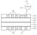
도 1을 참조하면, 상기 코어리스 인쇄회로기판(100)은 수지 절연층(101)과, 상기 수지 절연층(101)의 양면에 각각 표면이 노출되어 매립된, 랜드(103, 105)를 포함하는 회로 패턴(102, 104)과, 그리고 층간 전기적 접속을 위하여 각 층의 랜드(103, 105)와 접촉하도록 형성된 비아(106)를 포함한다.Referring to FIG. 1, the coreless printed
상기 수지 절연층(101)은 바람직하게는 보강재가 함침되거나 함침되지 않은 열경화성 수지로 이루어질 수 있으며, 예를 들어, 프리프레그, 또는 통상의 수지 기판 자재로서 FR-4, BT(Bismaleimide Triazine), ABF(Ajinomoto Build up Film) 등의 에폭시계 수지를 사용할 수 있으나, 특별히 이에 한정되는 것은 아니다. 일 반적으로는 양면 기판용으로 사용하는 경우에는 프리프레그를, 고다층 기판용으로 사용하는 경우에는 유리섬유가 함침되지 않은 열경화성 수지를 사용하나, 고다층 기판에서도 소정의 강도가 요구되는 경우에는 유리섬유가 함침된 수지를 사용하는 것이 바람직하다.The
상기 랜드(103, 105)를 포함하는, 양면의 회로 패턴(102, 104)은 하나의 동일한 수지 절연층(101)에 적층되어, 동시에 경화, 매립된다. 상기 회로 패턴(102, 104)의 폭(D)과 스페이스(E)는 실질적으로 동일하며, 특별히 한정되는 것은 아니지만, 고밀도 박판으로의 적용이 가능하도록 5∼15㎛ 사이의 범위에서 선택될 수 있다. 상기 회로 패턴(102, 104) 폭의 편차는 ±10% 이내인 것이 바람직하다.The
본 발명에 따르면, 상기 랜드(103, 105)를 포함하는, 회로 패턴(102, 104)의 노출된 표면 및 매립된 면 중 측면(I)에는 요철이 형성되어 있지 않고 내측 하단(J)에만 요철이 형성된다. 요철의 구조는 특별히 한정되는 것은 아니며, 예를 들어, 침상 또는 앵커 구조가 가능하다.According to the present invention, irregularities are not formed on the side surface I of the exposed and buried surfaces of the
상기 랜드(103, 105)를 포함하는, 각 회로 패턴(102, 104)의 두께(B, B')는 전기 도통의 문제가 없는 정도라면 특별히 한정되지 않으며, 양면의 회로 패턴(102, 104) 사이의 절연 거리(C) 또한 회로의 마이그레이션이 발생하지 않는 두께 이상이라면 특별히 한정되지 않고 적절히 선택될 수 있다.The thicknesses B and B 'of the
한편, 상기 회로 패턴(102, 104)과 비아(106)는 그 층 구성이 서로 다르다.On the other hand, the
바람직하게는, 상기 랜드(103, 105)를 포함하는 회로 패턴(102, 104)은 전해 동도금층으로 이루어지며, 상기 비아(106)는 내측 표면에 형성된 무전해 동박 시드 층(106a)과 상기 무전해 동박 시드층(106a)에 형성된 충전 도금층(106b)으로 이루어진다.Preferably, the
상기 랜드(103, 105)의 크기(F, F')는 비아(106)의 크기(G)와 에뉼러 링 크기(Anular ring size)(H)의 2배를 합한 값과 실질적으로 같다. 예를 들어, 고밀도 박판의 구조로 적용하기 위하여 상기 비아(106)의 크기(G)는 약 40∼65㎛으로 설정할 수 있고, 상기 에뉼러 링 크기(H)는 약 10∼30㎛으로 설정할 수 있으며, 이때 상기 랜드(103, 105)의 크기(F, F')는 (40∼65㎛)+(10∼30㎛)×2≒60∼125㎛일 수 있으나, 특별히 이에 한정되는 것은 아니다.The sizes F and F 'of the
한편, 상기 수지 절연층(101)과 상기 랜드(103, 105)를 포함하는, 노출된 회로 패턴(102, 104)의 표면 사이에는 약간의 단차(K, K')가 존재할 수 있다.Meanwhile, there may be some steps K and K ′ between the
이와 같이 구성되는 본 발명의 바람직한 일 실시형태에 따른 코어리스 기판(100)의 전체 두께(A)는 60㎛ 이하도 가능하다.60 micrometers or less of the total thickness A of the coreless board |
도 2a 내지 도 2b에 본 발명의 바람직한 일 실시형태에 따른 다층 코어리스 인쇄회로기판의 구조를 개략적으로 나타내었다.2A to 2B schematically show the structure of a multilayer coreless printed circuit board according to a preferred embodiment of the present invention.
본 발명에 따른 코어리스 인쇄회로기판은 외층 형성 시 일면 및 그 대면의 회로와 동일한 구조로 쌓아 올려지게 되며, 고다층일 경우 대칭구조로 형성해 나가는 것이 전형적이다.Coreless printed circuit board according to the present invention is stacked in the same structure as the circuit on one side and the surface when forming the outer layer, it is typical to form a symmetrical structure in the case of a high layer.
우선, 도 2a를 참조하여 6층의 다층 기판을 설명하면, 도 1의 내층 기판의 양면에 제1외층으로서, 제2의 수지 절연층(201)과, 상기 제2의 수지 절연층(201)에 표면이 노출되어 매립된, 제2의 랜드(203)를 포함하는 제2의 회로 패턴(202)과, 그리고 층간 전기적 접속을 위하여 랜드(203)와 접촉하도록 형성된 비아(206)를 포함한다. 또한, 상기 제1외층의 양면에 제2외층으로서, 제3의 수지 절연층(211)과, 상기 제3의 수지 절연층(211)에 표면이 노출되어 매립된, 제2의 랜드(213)를 포함하는 제3의 회로 패턴(212)과, 그리고 층간 전기적 접속을 위하여 랜드(213)와 접촉하도록 형성된 비아(216)를 포함한다.First, referring to FIG. 2A, a six-layered multilayer substrate will be described. As a first outer layer, a second
상기 제1외층에서, 상기 제2의 랜드(203)를 포함하는 제2의 회로 패턴(202)의 노출된 표면 및 매립된 면 중 측면에는 요철이 형성되어 있지 않고 내측 하단에만 요철이 형성되어 있으며, 상기 제2의 제2의 회로 패턴(202)과 상기 제2의 비아(206)는 층 구성이 각각 서로 다르다. 이는 제2외층에도 동일하게 적용된다.In the first outer layer, irregularities are not formed at the side surface of the exposed surface and the embedded surface of the
기판의 외층 구조의 각 부분에 사용되는 재료, 회로 패턴, 비아를 포함하는 구조적 사양은 도 1의 내층 구조에서 상술한 바에 따라 외층 구조에서도 실질적으로 동일하게 적용될 수 있다. 본 도면에서는 양면 6층 기판을 일례로 들어 설명하였으나, 이에 한정되지 않고 필요에 따라 다양한 층수의 다층 기판 제작이 가능하며, 또한 양면 뿐 아니라 단면에만 외층을 더욱 형성할 수 있음은 물론이다.Structural specifications, including materials, circuit patterns, and vias used in each portion of the outer layer structure of the substrate, may be applied substantially the same to the outer layer structure as described above in the inner layer structure of FIG. 1. In this drawing, the double-sided six-layer substrate has been described as an example, but not limited to this, it is possible to manufacture a multi-layered substrate having a variety of layers as necessary, and further, the outer layer may be further formed not only on both sides but also on one side.
도 2b는 최외층에 비아 랜드(203)가 없는 경우의 4층 기판을 나타낸 것으로서, 최외층에 비아 랜드를 형성하지 않은 것을 제외하고는 각 부분에 사용되는 재료, 회로 패턴, 비아를 포함하는 구조적 사양은 도 2a에서 상술한 바와 같다.FIG. 2B shows a four-layer substrate in the case where no via
한편, 상술한 코어리스 인쇄회로기판의 제조에 사용되는, 본 발명의 바람직 한 일 실시형태에 따른 회로 전사용 캐리어 부재는 캐리어층의 일면에 베리어층과, 랜드를 포함하거나 포함하지 않는 회로 패턴을 갖는다. 이때, 상기 랜드를 포함하거나 포함하지 않는 회로 패턴의 내측 하단 및 노출된 표면 중 측면에는 요철이 형성되어 있지 않고 외측 상단에만 요철이 형성되어 있다.On the other hand, the carrier member for circuit transfer according to the preferred embodiment of the present invention, which is used in the manufacturing of the coreless printed circuit board described above, has a circuit pattern including or not including a barrier layer and land on one surface of the carrier layer. Have In this case, irregularities are not formed at the side of the inner lower end and the exposed surface of the circuit pattern including or not including the land, and the irregularities are formed only at the outer upper end.
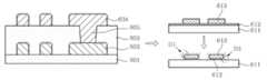
이하, 도 3a 내지 도 3e를 참조하여, 본 발명의 바람직한 일 실시형태에 따른 회로 전사용 캐리어 부재의 제조방법을 설명한다.Hereinafter, with reference to FIGS. 3A-3E, the manufacturing method of the carrier member for circuit transfer which concerns on one Embodiment of this invention is demonstrated.
우선, 열접착제(301)의 양면에 캐리어층(302a, 302b) 및 베리어층(303a, 303b)으로 구성된 캐리어 원판이 부착된 양면 캐리어 구조물(300)을 준비한다(도 3a 참조).First, a double-
상기 열접착제(301)는 열처리 시 비접착성을 나타내는 물질로서, 상온에서는 접착된 상태 그대로의 접착성을 유지하다가 열처리에 의해 접착성을 잃어 피접착물과의 박리가 가능한 것이라면 특별히 한정되지 않고 당업계에 공지된 모든 열접착제를 사용할 수 있다. 예를 들어, 약 100∼150℃의 온도에서의 열처리 시 비접착성을 나타내는 아크릴과 발포제로 이루어진 열접착제 등이 사용 가능하나, 특별히 이에 한정되는 것은 아니다.The
상기 캐리어층(302a, 302b)은 당업계에 공지된 것이라면 특별히 한정되지 않고 사용할 수 있으며, 예를 들어, 금속 또는 중합체, 특히 박리성 중합체로 이루어진 재료 모두 사용 가능하다.The carrier layers 302a and 302b can be used without particular limitations as long as they are known in the art, and for example, metals or polymers, in particular, materials made of a peelable polymer can be used.
상기 베리어층(303a, 303b)은 당업계에서 구리 이외의 금속으로서 베리어층 으로서 사용 가능한 것이라면 특별히 한정되지 않으며, 예를 들어, 니켈, 크롬, 이들의 조합 등을 들 수 있으나, 특별히 이에 한정되는 것은 아니다. 또한, 상기 베리어층의 두께 및 형성방법은 특별히 한정되지 않는다. 예를 들어, 상기 베리어층(303a, 303b)은 전해 또는 무전해 도금을 통해서 약 3∼5㎛의 두께로 형성될 수 있으나, 특별히 이에 한정되는 것은 아니다.The barrier layers 303a and 303b are not particularly limited as long as they can be used as barrier layers as metals other than copper in the art, and examples thereof include nickel, chromium, a combination thereof, and the like. no. In addition, the thickness and the formation method of the barrier layer are not particularly limited. For example, the
이어서, 상기 양면 캐리어 구조물(300)의 베리어층(303a, 303b) 상에, 랜드를 포함하거나 포함하지 않는 회로 형성 부위(305, 306, 307, 308)를 제외한 부분에 도금레지스트(304a, 304b)를 도포한다(도 3b 참조). 상기 도금레지스트(304a, 304b)로는 당업계에 공지된 것이라면 특별히 한정되지 않고 사용 가능하며, 예를 들어, 드라이필름을 사용하여 통상의 노광/에칭 과정을 통해서 회로 형성 부위만을 오픈시킬 수 있다.Subsequently, plating resists 304a and 304b are formed on the
이때, 상기 회로 형성 부위(305, 306, 307, 308)는, 바람직하게는, 상기 회로 전사용 캐리어 부재 중 하나의 회로 전사용 캐리어 부재에 형성된 제1층 랜드(312)가 비아홀 가공 부위를 사이에 두고 이격되어 패턴화되며, 다른 하나의 회로 전사용 캐리어 부재에 형성된 제2층 랜드(310)가 이격 부분 없이 일체로 상기 제1층 랜드(312)에 대향되어 형성되도록 선택된다.In this case, the
다음, 상기 도금레지스트(304a, 304b)를 통해서 오픈된 회로 형성 부위(305, 306, 307, 308)에 통상의 전해 동도금을 수행하여 회로 패턴(309, 310, 311, 312)을 형성한다(도 3c 참조). 이때, 베리어층(303a, 303b)이 이미 형성되어 있기 때문에 별도의 시드층 형성 과정없이 바로 전해 동도금이 가능하다.Next, ordinary electrolytic copper plating is performed on the
이어서, 상기 회로 패턴의 노출된 표면을 조도처리하여 요철(313)을 형성한다(도 3d 참조). 상기 조도처리는 당업계에서 수지 절연층와 회로층과의 접착력 향상을 위하여 사용되는 방법이라면 특별히 한정되지 않고 모두 사용 가능하며, 이로부터 형성되는 요철(313)의 형상은 특별히 한정되지 않고, 예를 들어, 침상 또는 앵커 구조로 형성될 수 있다.The exposed surface of the circuit pattern is then roughened to form the unevenness 313 (see FIG. 3D). The roughness treatment is not particularly limited and can be used as long as it is a method used for improving adhesion between the resin insulating layer and the circuit layer in the art, and the shape of the
다음, 상기 도금레지스트(304a, 304b)를 박리 등을 통해서 제거하고, 상기 양면 캐리어 구조물(300)을 열처리하여, 바람직하게는 약 100∼150℃의 온도에서 열처리하여 열접착제(301)로부터 한 쌍의 회로 전사용 캐리어 부재(C1, C2)를 각각 분리하여 얻는다. 상기 한 쌍의 회로 전사용 캐리어 부재(C1, C2)의 경우, 랜드(310, 312)를 포함하는 회로 패턴(309, 311)의 구조적 사양은 도 1에서 상술한 바와 같다.Next, the plating resists 304a and 304b are removed by peeling or the like, and the double-
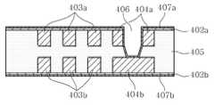
이하, 도 4a 내지 도 4g를 참조하여, 상기 회로 전사용 캐리어 부재를 이용하여 코어리스 인쇄회로기판을 제조하는 방법의 바람직한 일 실시형태를 설명한다.4A to 4G, a preferred embodiment of a method for manufacturing a coreless printed circuit board using the carrier member for circuit transfer will be described.
우선, 상술한 바에 따라 제작되어, 캐리어층(401a, 401b)의 일면에 베리어층(402a, 402b), 및 랜드(404a, 404b)를 포함하는 회로 패턴(403a, 403b)을 갖는 한 쌍의 회로 전사용 캐리어 부재(400a, 400b)를 준비한다. 바람직하게는, 상기 한 쌍의 회로 전사용 캐리어 부재 중 제1의 회로 전사용 캐리어 부재(400a)에 형성된 제1층 랜드(404a)는 비아홀(406)과 양 측면에서 접촉면을 갖도록 비아홀 가공 부위를 사이에 두고 이격되어 형성되며, 제2의 회로 전사용 캐리어 부재(400b)에 형성된 제2층 랜드(404b)는 내측 상단에서 비아홀(406)과 접촉면을 갖도록 이격 부분 없이 일체로 상기 제1층 랜드(404a)에 대향되어 형성된다.First, as described above, a pair of circuits having
이때, 상기 랜드(404a, 404b)를 포함하는 회로 패턴(403a, 403b)의 내측 하단 및 노출된 표면 중 측면에는 요철(R)이 형성되어 있지 않고 외측 상단에만 요철(R)이 형성되어 있다.At this time, the unevenness R is not formed at the inner side lower end and exposed side surfaces of the
다음, 수지 절연층(405)을 준비하고, 상기 한 쌍의 회로 전사용 캐리어 부재(400a, 400b)를 회로 패턴(403a, 403b, 404a, 404b)이 내층으로 향하도록 서로 대향시켜 상기 수지 절연층(405)에 회로 패턴(403a, 403b, 404a, 404b)을 각각 매립한다 (도 4a 참조). 이때, 상기 한 쌍의 회로 전사용 캐리어 부재(400a, 400b)는 하나의 수지 절연층(405)에 대향시켜 적층하고, 수지 절연층(405)을 경화시켜 매립한다.Next, a
이어서, 상기 회로 전사용 캐리어 부재(400a, 400b)의 캐리어층(401a, 401b)을 각각 제거하여 베리어층(402a, 402b)을 노출시킨다(도 4b 참조). 상기 캐리어층(401a, 401b)의 제거는 경화/매립이 완료된 후, 예를 들어, 캐리어층으로서 박리성 중합체를 사용한 경우에는 박리(peeling)를 사용하거나, 또는 금속 재질의 캐리어층을 사용한 경우에는 통상의 에칭을 통해서 제거할 수 있으나, 특별히 이에 한정되는 것은 아니다.Subsequently, the carrier layers 401a and 401b of the circuit
다음, 층간 전기적 접속을 위한 비아홀(406)을 가공하여 랜드(404a, 404b)의 접촉면을 노출시킨다(도 4c 참조). 이때, 상기 비아홀(406) 가공은 통상의 CO2 레 이저 등을 사용하여 수행될 수 있다. 바람직하게는, 상기 비아홀(406) 가공은 먼저 비아를 형성할 부위의 베리어층(402a)을 제거하여 수지 절연층(405)을 노출시킨 후, 수지 절연층(405)을 가공하여 랜드(404a, 404b)의 접촉면을 노출시켜 수행될 수 있다.Next, via
이어서, 상기 비아홀(406) 내부를 포함하여 베리어층(402a, 402b) 상에 구리 시드층(407a, 407b)을 각각 형성한다(도 4d 참조). 상기 구리 시드층(407a, 407b) 형성은 무전해 동도금을 통해서 수행될 수 있으나, 특별히 이에 한정되는 것은 아니다. 이때, 무전해 동도금 전에 노출된 표면의 이물질 등을 제거하기 위하여 예를 들어, 디스미어 처리와 같은 통상의 표면 전처리를 수행할 수 있다.Subsequently,
다음, 상기 비아홀 내부를 충전 도금(408)한다(도 4e 참조). 상기 충전 도금방법으로는 특별히 한정되는 것은 아니나, 예를 들어, 역펄스 도금과 같이 도금액 성분 및 도금 방법 등을 적절히 조절하여 주로 비아 내에 충전 도금층이 형성되고, 기판 표면에는 도금층이 거의 형성되지 않도록 하는 것이 바람직하다.Next, the inside of the via hole is plated 408 (see FIG. 4E). The filling plating method is not particularly limited, but, for example, the plating liquid component and the plating method may be appropriately adjusted, such as reverse pulse plating, so that the filling plating layer is mainly formed in the via, and the plating layer is hardly formed on the substrate surface. It is preferable.
이어서, 상기 구리 시드층(407a, 407b)을 포함하는 표면층을 통상의 플레시 에칭 등의 방법을 이용하여 에칭하여 베리어층(402a, 402b)을 노출시킨다(도 4f 참조). 상기 베리어층(402a, 402b)을 포함하는 표면층 역시 통상의 금속 에칭법을 통해서 에칭하여 회로 패턴(403a, 403b, 404a, 404b)을 노출시킨다(도 4g 참조). 이때, 기존의 방법에 따라 구리 시드층을 에칭하는 것에 비해서, 본 발명에 따라 구리 이외의 금속으로 이루어지는 베리어층을 에칭하여 제거하는 경우 구리 회로 패턴 부위의 손상을 줄일 수 있다. 한편, 상기 베리어층(402a, 402b)을 에칭하는 과정에서 통상적으로 회로의 표면도 미세하게 에칭되기 때문에 수지 절연층(405) 표면과 회로 표면간에 약간의 단차가 생성될 수 있다.Subsequently, the surface layer including the
본 발명에 따르면, 코어리스 기판을 제작하면서도 일정 수준의 기판 강도를 유지할 수 있어, 상술한 코어리스 인쇄회로기판의 제조과정을 구동 롤(roll)에 접촉이 작은 라인으로, 즉 시트 타입(sheet type)의 공정으로 수행할 수 있다.According to the present invention, while manufacturing a coreless substrate, it is possible to maintain a certain level of substrate strength, so that the process of manufacturing the coreless printed circuit board described above is a line having a small contact with a driving roll, that is, a sheet type. Can be carried out in the process of).
본 도면에서는 코어 구조의 기판만을 예를 들어 설명하였으나, 이에 한정되지 않고, 상기 도 3a 내지 3e에 나타낸 바에 따라 제작된 또 다른 회로 전사용 캐리어 부재를 사용하여 상기 코어리스 기판의 단면 또는 양면에 제2의 수지 절연층을 적층하고, 여기에 제2의 회로 패턴을 상술한 방법에 따라, 매립, 전사하고 층간 연결을 위한 비아를 형성하여 외층을 형성하는 과정을 수회 반복하여 다층 인쇄회로기판을 구현할 수 있음은 물론이다. 이때, 최외층에는 필요에 따라 비아 랜드를 생략하여 제작할 수 있다.In the drawing, only the core structured substrate has been described as an example. However, the present invention is not limited thereto, and the circuit member may be formed on one or both surfaces of the coreless substrate using another carrier member for circuit transfer manufactured as shown in FIGS. 3A to 3E. The multilayer printed circuit board may be repeatedly formed by laminating the resin insulating layer of 2 and forming the outer layer by filling the second circuit pattern, embedding, transferring, and forming vias for interlayer connection. Of course it can. At this time, via land may be omitted and produced in outermost layer as needed.
위에서 살펴본 바와 같이, 본 발명에 따르면, 회로가 절연층에 묻혀 있는 구조로서, 실질적인 코어 없이 미세 회로를 갖는 얇은 코어 기판 구조의 구현이 가능하다. 또한, 매립된 회로의 내측 하부에만 회로 밀착력을 높이기 위한 조도 처리가 되어 있어 회로의 손상을 최소화하는 동시에 신뢰성을 높일 수 있다.As described above, according to the present invention, the circuit is buried in the insulating layer, it is possible to implement a thin core substrate structure having a fine circuit without a substantial core. In addition, only the inner lower part of the buried circuit is provided with an illuminance treatment to increase the circuit adhesion, thereby minimizing damage to the circuit and increasing reliability.
또한, 코어 구조에서 일면과 타면의 회로층이 하나의 절연층에 매립되어 구현되기 때문에 동시에 경화되어 형성되는 구조로서, 박판의 고밀도 인쇄회로기판의 제작이 가능하다.In addition, since the circuit layer of one side and the other side of the core structure is implemented by embedding in one insulating layer, the structure is formed by curing at the same time, it is possible to manufacture a thin high-density printed circuit board.
이상 본 발명을 구체적인 실시예를 통하여 상세히 설명하였으나, 이는 본 발명을 구체적으로 설명하기 위한 것으로, 본 발명에 따른 회로 전사용 캐리어 부재, 이를 이용한 코어리스 인쇄회로기판, 및 이들의 제조방법은 이에 한정되지 않으며, 본 발명의 기술적 사상 내에서 당 분야의 통상의 지식을 가진 자에 의해 그 변형이나 개량이 가능함이 명백하다.Although the present invention has been described in detail with reference to specific embodiments, this is for explaining the present invention in detail, and the carrier member for circuit transfer according to the present invention, a coreless printed circuit board using the same, and a manufacturing method thereof are limited thereto. It is apparent that modifications and improvements are possible by those skilled in the art within the technical idea of the present invention.
전술한 바와 같이, 본 발명에 따르면, 미세 회로를 구현하는데 있어서 시드층 제거 시 회로의 손상이 최소화되어 유리하다. 또한, 미세 회로의 매립된 내측 하부만 회로 밀착력을 높이기 위한 요철이 형성되기 때문에 회로 손상을 최소화하는 동시에 고 신뢰성의 기판 구조를 제작할 수 있다.As described above, according to the present invention, it is advantageous to minimize the damage of the circuit when removing the seed layer in implementing the fine circuit. In addition, since only the inner bottom portion of the microcircuit is formed with the unevenness to increase the circuit adhesion, it is possible to minimize the circuit damage and to produce a highly reliable substrate structure.
나아가, 캐리어를 통해서 회로를 제작한 후, 회로를 수지 절연층 내에 전사/매립하여 형성함으로써 실질적인 코어 없이 내층의 코어 기판을 제작할 수 있다. 아울러, 제조 라인에서 기판에 일정 수준 이상의 강도가 확보되어 얇은 기판을 구동하기 위한 별도의 설비가 요구되지 않으며, 구동 롤에 접촉이 적은 시트 타입의 공정 라인으로 제작할 수 있는 이점이 있다.Furthermore, after fabricating a circuit through a carrier, the core substrate of an inner layer can be produced without a substantial core by transferring and embedding the circuit in a resin insulating layer. In addition, since a certain level of strength is secured to a substrate in a manufacturing line, a separate facility for driving a thin substrate is not required, and there is an advantage in that it can be manufactured in a sheet-type process line with less contact with a driving roll.
뿐만 아니라, 기존의 인쇄회로기판에 비해서 기판 표면이 평탄하기 때문에 IC 실장에 유리하다.In addition, since the surface of the substrate is flat compared to the conventional printed circuit board, it is advantageous for IC mounting.
본 발명의 단순한 변형 내지 변경은 모두 본 발명의 영역에 속하는 것으로 본 발명의 구체적인 보호 범위는 첨부된 특허청구범위에 의하여 명확해질 것이다.All simple modifications and variations of the present invention fall within the scope of the present invention, and the specific scope of protection of the present invention will be apparent from the appended claims.
Claims (26)
Translated fromKoreanPriority Applications (7)
| Application Number | Priority Date | Filing Date | Title |
|---|---|---|---|
| KR1020070042002AKR100905566B1 (en) | 2007-04-30 | 2007-04-30 | Carrier member for circuit transfer, coreless printed circuit board using the same, and manufacturing method thereof |
| JP2007337587AJP4646968B2 (en) | 2007-04-30 | 2007-12-27 | Method for manufacturing carrier member for circuit transfer |
| US12/003,669US20080264684A1 (en) | 2007-04-30 | 2007-12-28 | Carrier member for transmitting circuits, coreless printed circuit board using the carrier member, and method of manufacturing the same |
| TW096150792ATWI352562B (en) | 2007-04-30 | 2007-12-28 | Carrier member for transmitting circuits, coreless |
| JP2010163108AJP2010263237A (en) | 2007-04-30 | 2010-07-20 | Carrier member for transmitting circuit, coreless printed circuit board using the same, and method of manufacturing the same |
| US13/311,058US20120073865A1 (en) | 2007-04-30 | 2011-12-05 | Carrier member for transmitting circuits, coreless printed circuit board using the carrier member, and method of manufacturing the same |
| JP2013000173AJP2013062546A (en) | 2007-04-30 | 2013-01-04 | Carrier member for transmitting circuit, coreless printed circuit board using the same, and method of manufacturing the same |
Applications Claiming Priority (1)
| Application Number | Priority Date | Filing Date | Title |
|---|---|---|---|
| KR1020070042002AKR100905566B1 (en) | 2007-04-30 | 2007-04-30 | Carrier member for circuit transfer, coreless printed circuit board using the same, and manufacturing method thereof |
Publications (2)
| Publication Number | Publication Date |
|---|---|
| KR20080096985A KR20080096985A (en) | 2008-11-04 |
| KR100905566B1true KR100905566B1 (en) | 2009-07-02 |
Family
ID=39885649
Family Applications (1)
| Application Number | Title | Priority Date | Filing Date |
|---|---|---|---|
| KR1020070042002AExpired - Fee RelatedKR100905566B1 (en) | 2007-04-30 | 2007-04-30 | Carrier member for circuit transfer, coreless printed circuit board using the same, and manufacturing method thereof |
Country Status (4)
| Country | Link |
|---|---|
| US (2) | US20080264684A1 (en) |
| JP (3) | JP4646968B2 (en) |
| KR (1) | KR100905566B1 (en) |
| TW (1) | TWI352562B (en) |
Cited By (2)
| Publication number | Priority date | Publication date | Assignee | Title |
|---|---|---|---|---|
| KR101179716B1 (en) | 2010-10-28 | 2012-09-04 | 삼성전기주식회사 | Printed Circuit Board AND Manufacturing Method for Printed Circuit Board |
| US11026327B2 (en) | 2017-07-28 | 2021-06-01 | Lg Innotek Co., Ltd. | Printed circuit board |
Families Citing this family (42)
| Publication number | Priority date | Publication date | Assignee | Title |
|---|---|---|---|---|
| US20100073894A1 (en)* | 2008-09-22 | 2010-03-25 | Russell Mortensen | Coreless substrate, method of manufacturing same, and package for microelectronic device incorporating same |
| KR101013992B1 (en) | 2008-12-02 | 2011-02-14 | 삼성전기주식회사 | Printed Circuit Board Manufacturing Method |
| KR101095211B1 (en) | 2008-12-17 | 2011-12-16 | 삼성전기주식회사 | Carrier member for substrate manufacturing and substrate manufacturing method using same |
| US8872329B1 (en)* | 2009-01-09 | 2014-10-28 | Amkor Technology, Inc. | Extended landing pad substrate package structure and method |
| KR101119308B1 (en)* | 2009-02-03 | 2012-03-19 | 삼성전기주식회사 | A printed circuit board and a fabricating method the same |
| US9930775B2 (en)* | 2009-06-02 | 2018-03-27 | Hsio Technologies, Llc | Copper pillar full metal via electrical circuit structure |
| KR20110037332A (en)* | 2009-10-06 | 2011-04-13 | 삼성전기주식회사 | Printed circuit board and manufacturing method thereof |
| TWI392405B (en)* | 2009-10-26 | 2013-04-01 | Unimicron Technology Corp | Circuit structure |
| KR101136394B1 (en)* | 2009-11-11 | 2012-04-18 | 엘지이노텍 주식회사 | Manufacturing method of printed circuit board |
| KR101203965B1 (en)* | 2009-11-25 | 2012-11-26 | 엘지이노텍 주식회사 | Printed circuit board and manufacturing method of the same |
| KR101158494B1 (en)* | 2009-11-25 | 2012-06-21 | 엘지이노텍 주식회사 | PCB and Fabricating Method of the same |
| KR101086828B1 (en) | 2009-11-30 | 2011-11-25 | 엘지이노텍 주식회사 | Embedded printed circuit boards, multilayer printed circuit boards and methods of manufacturing the same |
| US9496152B2 (en)* | 2010-03-12 | 2016-11-15 | STATS ChipPAC Pte. Ltd. | Carrier system with multi-tier conductive posts and method of manufacture thereof |
| JP5392167B2 (en)* | 2010-04-02 | 2014-01-22 | 富士通株式会社 | Electronic parts and manufacturing method thereof |
| JP5602584B2 (en)* | 2010-10-28 | 2014-10-08 | 新光電気工業株式会社 | Wiring board and manufacturing method thereof |
| KR101216864B1 (en) | 2010-12-29 | 2012-12-28 | 한국이엔에쓰 주식회사 | Printed circuit board and manufacturing method of the same |
| KR101231382B1 (en)* | 2011-08-03 | 2013-02-07 | 엘지이노텍 주식회사 | The printed circuit board and the method for manufacturing the same |
| US8841209B2 (en)* | 2011-08-18 | 2014-09-23 | International Business Machines Corporation | Method for forming coreless flip chip ball grid array (FCBGA) substrates and such substrates formed by the method |
| US20130118794A1 (en)* | 2011-11-15 | 2013-05-16 | Bo-Yu Tseng | Package Substrate Structure |
| KR101326999B1 (en)* | 2012-03-07 | 2013-11-13 | 엘지이노텍 주식회사 | The printed circuit board and the method for manufacturing the same |
| US8517769B1 (en)* | 2012-03-16 | 2013-08-27 | Globalfoundries Inc. | Methods of forming copper-based conductive structures on an integrated circuit device |
| US9768102B2 (en) | 2012-03-21 | 2017-09-19 | STATS ChipPAC Pte. Ltd. | Integrated circuit packaging system with support structure and method of manufacture thereof |
| US8673766B2 (en) | 2012-05-21 | 2014-03-18 | Globalfoundries Inc. | Methods of forming copper-based conductive structures by forming a copper-based seed layer having an as-deposited thickness profile and thereafter performing an etching process and electroless copper deposition |
| KR20140008923A (en)* | 2012-07-13 | 2014-01-22 | 삼성전기주식회사 | Coreless substrate and method of manufacturing the same |
| CN103717010A (en)* | 2012-10-08 | 2014-04-09 | 苏州卓融水处理科技有限公司 | Processing method for enhancing adhesive force of seed layer of corelessly-packaged substrate |
| US8975665B2 (en) | 2012-10-10 | 2015-03-10 | Stats Chippac Ltd. | Integrated circuit packaging system with coreless substrate and method of manufacture thereof |
| KR20140060767A (en)* | 2012-11-12 | 2014-05-21 | 삼성전기주식회사 | Circuit board and method for manufacturing the same |
| JP6291738B2 (en) | 2013-07-25 | 2018-03-14 | 富士通株式会社 | CIRCUIT BOARD, CIRCUIT BOARD MANUFACTURING METHOD, AND ELECTRONIC DEVICE |
| KR102107037B1 (en) | 2014-02-21 | 2020-05-07 | 삼성전기주식회사 | Printed circuit board and method of manufacturing the same |
| TWI517775B (en)* | 2014-03-06 | 2016-01-11 | 相互股份有限公司 | Printed circuit board and method thereof |
| JP2016115823A (en)* | 2014-12-16 | 2016-06-23 | イビデン株式会社 | Printed wiring board |
| CN208159009U (en)* | 2015-11-10 | 2018-11-27 | 株式会社村田制作所 | resin multilayer substrate |
| JP2018171899A (en)* | 2017-03-31 | 2018-11-08 | Jx金属株式会社 | Copper foil with release layer, laminate, method for producing printed wiring board and method for producing electronic apparatus |
| JP2018171902A (en)* | 2017-03-31 | 2018-11-08 | Jx金属株式会社 | Copper foil with release layer, laminate, method for producing printed wiring board and method for producing electronic apparatus |
| JP6856444B2 (en)* | 2017-05-12 | 2021-04-07 | 新光電気工業株式会社 | Wiring board, manufacturing method of wiring board |
| KR20190065748A (en)* | 2017-12-04 | 2019-06-12 | 삼성전기주식회사 | Printed circuit board |
| KR102298165B1 (en)* | 2018-03-14 | 2021-09-06 | 주식회사 엘지화학 | Embedded transparent electrode substrate and method for manufacturing thereof |
| KR102752625B1 (en)* | 2019-02-15 | 2025-01-10 | 엘지이노텍 주식회사 | Circuit board |
| KR20220086257A (en)* | 2020-12-16 | 2022-06-23 | 엘지이노텍 주식회사 | Circuit board and mehod of manufacturing thereof |
| WO2022202547A1 (en)* | 2021-03-22 | 2022-09-29 | パナソニックIpマネジメント株式会社 | Wiring body, mounting substrate, method for manufacturing wiring body, and method for manufacturing mounting substrate |
| JP2023010237A (en)* | 2021-07-09 | 2023-01-20 | イビデン株式会社 | Wiring board and method for manufacturing wiring board |
| US11791320B2 (en)* | 2021-11-22 | 2023-10-17 | Qualcomm Incorporated | Integrated circuit (IC) packages employing a package substrate with a double side embedded trace substrate (ETS), and related fabrication methods |
Citations (4)
| Publication number | Priority date | Publication date | Assignee | Title |
|---|---|---|---|---|
| KR20010006456A (en)* | 1997-04-16 | 2001-01-26 | 고토 기치 | Polyolefin resin composition |
| KR20040086838A (en)* | 2003-04-04 | 2004-10-12 | 가부시키가이샤 덴소 | Multi-layer printed circuit board and method for manufacturing the same |
| KR20050085879A (en)* | 2002-12-24 | 2005-08-29 | 티디케이가부시기가이샤 | Electronic part manufacturing method and electronic part |
| KR20060018262A (en)* | 2003-09-29 | 2006-02-28 | 이비덴 가부시키가이샤 | Interlayer insulation layer for printed wiring boards, printed wiring boards and manufacturing method thereof |
Family Cites Families (22)
| Publication number | Priority date | Publication date | Assignee | Title |
|---|---|---|---|---|
| JPH02159789A (en)* | 1988-12-14 | 1990-06-19 | Meiko Denshi Kogyo Kk | Manufacture of printed wiring board |
| JPH03196597A (en)* | 1989-12-25 | 1991-08-28 | Matsushita Electric Works Ltd | Manufacture of printed wiring board |
| JPH06177277A (en)* | 1992-12-08 | 1994-06-24 | Toppan Printing Co Ltd | Method for manufacturing semiconductor device |
| JPH06232516A (en)* | 1993-02-04 | 1994-08-19 | Ngk Insulators Ltd | Ceramic wiring board and manufacture thereof |
| JPH1032371A (en)* | 1996-05-17 | 1998-02-03 | Furukawa Electric Co Ltd:The | Composite circuit board and method of manufacturing the same |
| JP3431556B2 (en)* | 1999-12-07 | 2003-07-28 | 松下電器産業株式会社 | Transfer medium, method of manufacturing the same, and method of manufacturing wiring board using transfer medium |
| JP2001251060A (en)* | 2000-03-02 | 2001-09-14 | Sony Corp | Multilayer printed wiring board |
| JP4062907B2 (en)* | 2001-11-12 | 2008-03-19 | 松下電器産業株式会社 | Circuit board and manufacturing method thereof |
| JP2003158371A (en)* | 2001-11-21 | 2003-05-30 | Matsushita Electric Ind Co Ltd | Circuit board and method of manufacturing the same |
| JP2003273510A (en)* | 2002-03-12 | 2003-09-26 | Hitachi Kokusai Electric Inc | Printed circuit board manufacturing method |
| JP4413522B2 (en)* | 2002-04-25 | 2010-02-10 | パナソニック株式会社 | Wiring transfer sheet and manufacturing method thereof, and wiring board and manufacturing method thereof |
| JP2004179540A (en)* | 2002-11-28 | 2004-06-24 | Fujikura Ltd | Manufacturing method of adhesive-free flexible metal laminate |
| JP2004256788A (en)* | 2002-11-29 | 2004-09-16 | Sekisui Chem Co Ltd | Thermally eliminable material |
| JP4193479B2 (en)* | 2002-12-04 | 2008-12-10 | ソニー株式会社 | Manufacturing method of element mounting substrate |
| US7001662B2 (en)* | 2003-03-28 | 2006-02-21 | Matsushita Electric Industrial Co., Ltd. | Transfer sheet and wiring board using the same, and method of manufacturing the same |
| JP2004319976A (en)* | 2003-03-28 | 2004-11-11 | Matsushita Electric Ind Co Ltd | Transfer sheet, wiring board using the same, and method of manufacturing the same |
| JP4488187B2 (en)* | 2003-06-27 | 2010-06-23 | Tdk株式会社 | Method for manufacturing substrate having via hole |
| JP3979391B2 (en)* | 2004-01-26 | 2007-09-19 | 松下電器産業株式会社 | Circuit forming substrate manufacturing method and circuit forming substrate manufacturing material |
| TWI347151B (en)* | 2004-03-19 | 2011-08-11 | Panasonic Corp | Flexible substrate having interlaminar junctions, and process for producing the same |
| JP4079927B2 (en)* | 2004-09-16 | 2008-04-23 | Tdk株式会社 | Multilayer substrate and manufacturing method thereof |
| US20060220167A1 (en)* | 2005-03-31 | 2006-10-05 | Intel Corporation | IC package with prefabricated film capacitor |
| JP4431123B2 (en)* | 2006-05-22 | 2010-03-10 | 日立電線株式会社 | Electronic device substrate and manufacturing method thereof, and electronic device and manufacturing method thereof |
- 2007
- 2007-04-30KRKR1020070042002Apatent/KR100905566B1/ennot_activeExpired - Fee Related
- 2007-12-27JPJP2007337587Apatent/JP4646968B2/ennot_activeExpired - Fee Related
- 2007-12-28TWTW096150792Apatent/TWI352562B/ennot_activeIP Right Cessation
- 2007-12-28USUS12/003,669patent/US20080264684A1/ennot_activeAbandoned
- 2010
- 2010-07-20JPJP2010163108Apatent/JP2010263237A/enactivePending
- 2011
- 2011-12-05USUS13/311,058patent/US20120073865A1/ennot_activeAbandoned
- 2013
- 2013-01-04JPJP2013000173Apatent/JP2013062546A/enactivePending
Patent Citations (4)
| Publication number | Priority date | Publication date | Assignee | Title |
|---|---|---|---|---|
| KR20010006456A (en)* | 1997-04-16 | 2001-01-26 | 고토 기치 | Polyolefin resin composition |
| KR20050085879A (en)* | 2002-12-24 | 2005-08-29 | 티디케이가부시기가이샤 | Electronic part manufacturing method and electronic part |
| KR20040086838A (en)* | 2003-04-04 | 2004-10-12 | 가부시키가이샤 덴소 | Multi-layer printed circuit board and method for manufacturing the same |
| KR20060018262A (en)* | 2003-09-29 | 2006-02-28 | 이비덴 가부시키가이샤 | Interlayer insulation layer for printed wiring boards, printed wiring boards and manufacturing method thereof |
Cited By (2)
| Publication number | Priority date | Publication date | Assignee | Title |
|---|---|---|---|---|
| KR101179716B1 (en) | 2010-10-28 | 2012-09-04 | 삼성전기주식회사 | Printed Circuit Board AND Manufacturing Method for Printed Circuit Board |
| US11026327B2 (en) | 2017-07-28 | 2021-06-01 | Lg Innotek Co., Ltd. | Printed circuit board |
Also Published As
| Publication number | Publication date |
|---|---|
| JP2008277737A (en) | 2008-11-13 |
| JP2013062546A (en) | 2013-04-04 |
| TWI352562B (en) | 2011-11-11 |
| US20120073865A1 (en) | 2012-03-29 |
| US20080264684A1 (en) | 2008-10-30 |
| JP2010263237A (en) | 2010-11-18 |
| KR20080096985A (en) | 2008-11-04 |
| TW200843578A (en) | 2008-11-01 |
| JP4646968B2 (en) | 2011-03-09 |
Similar Documents
| Publication | Publication Date | Title |
|---|---|---|
| KR100905566B1 (en) | Carrier member for circuit transfer, coreless printed circuit board using the same, and manufacturing method thereof | |
| US7768116B2 (en) | Semiconductor package substrate having different thicknesses between wire bonding pad and ball pad and method for fabricating the same | |
| US20080098597A1 (en) | Method of manufacturing circuit board | |
| JP4043115B2 (en) | Multi-layer printed wiring board | |
| JP2004311736A (en) | Manufacturing method of build-up multilayer wiring board with built-in chip components | |
| JPH1154934A (en) | Multilayered printed wiring board and its manufacture | |
| KR101148735B1 (en) | Printed circuit board and method of manufacturing the same | |
| KR100897650B1 (en) | Manufacturing method of multilayer printed circuit board | |
| JP4691763B2 (en) | Method for manufacturing printed wiring board | |
| US7278205B2 (en) | Multilayer printed wiring board and production method therefor | |
| KR20070035321A (en) | High density printed circuit board manufacturing method | |
| KR20070021631A (en) | Multilayer printed circuit board and its manufacturing method | |
| JP2010225973A (en) | Multilayer circuit board manufacturing method | |
| JPH1154926A (en) | One-sided circuit board and its manufacture | |
| KR20190008923A (en) | Method for manufacturing circuit boards | |
| KR101167422B1 (en) | Carrier member and method of manufacturing PCB using the same | |
| KR100722599B1 (en) | Full Layer Inner Via Printed Circuit Board Using Peel Plating and Its Manufacturing Method | |
| KR20100095742A (en) | Manufacturing method for embedded pcb, and embedded pcb structure using the same | |
| JP2001257476A (en) | Multilayer wiring board and manufacturing method thereof | |
| JP3645780B2 (en) | Build-up multilayer printed wiring board and manufacturing method thereof | |
| KR20120026368A (en) | Printed circuit board and method of manufacturing the same | |
| JP2549713B2 (en) | Method for manufacturing multilayer printed circuit board having blind through holes | |
| JPS62186595A (en) | Multilayer printed wiring board and manufacture of the same | |
| JP2000183528A (en) | Manufacture of multilayer printed wiring board | |
| KR100222753B1 (en) | Fabrication method of laminate pcb elevation isolation |
Legal Events
| Date | Code | Title | Description |
|---|---|---|---|
| A201 | Request for examination | ||
| PA0109 | Patent application | St.27 status event code:A-0-1-A10-A12-nap-PA0109 | |
| PA0201 | Request for examination | St.27 status event code:A-1-2-D10-D11-exm-PA0201 | |
| D13-X000 | Search requested | St.27 status event code:A-1-2-D10-D13-srh-X000 | |
| D14-X000 | Search report completed | St.27 status event code:A-1-2-D10-D14-srh-X000 | |
| E902 | Notification of reason for refusal | ||
| PE0902 | Notice of grounds for rejection | St.27 status event code:A-1-2-D10-D21-exm-PE0902 | |
| E13-X000 | Pre-grant limitation requested | St.27 status event code:A-2-3-E10-E13-lim-X000 | |
| P11-X000 | Amendment of application requested | St.27 status event code:A-2-2-P10-P11-nap-X000 | |
| P13-X000 | Application amended | St.27 status event code:A-2-2-P10-P13-nap-X000 | |
| E902 | Notification of reason for refusal | ||
| PE0902 | Notice of grounds for rejection | St.27 status event code:A-1-2-D10-D21-exm-PE0902 | |
| PG1501 | Laying open of application | St.27 status event code:A-1-1-Q10-Q12-nap-PG1501 | |
| E701 | Decision to grant or registration of patent right | ||
| PE0701 | Decision of registration | St.27 status event code:A-1-2-D10-D22-exm-PE0701 | |
| GRNT | Written decision to grant | ||
| PR0701 | Registration of establishment | St.27 status event code:A-2-4-F10-F11-exm-PR0701 | |
| PR1002 | Payment of registration fee | St.27 status event code:A-2-2-U10-U11-oth-PR1002 Fee payment year number:1 | |
| PG1601 | Publication of registration | St.27 status event code:A-4-4-Q10-Q13-nap-PG1601 | |
| PR1001 | Payment of annual fee | St.27 status event code:A-4-4-U10-U11-oth-PR1001 Fee payment year number:4 | |
| FPAY | Annual fee payment | Payment date:20130403 Year of fee payment:5 | |
| PR1001 | Payment of annual fee | St.27 status event code:A-4-4-U10-U11-oth-PR1001 Fee payment year number:5 | |
| FPAY | Annual fee payment | Payment date:20140325 Year of fee payment:6 | |
| PR1001 | Payment of annual fee | St.27 status event code:A-4-4-U10-U11-oth-PR1001 Fee payment year number:6 | |
| R18-X000 | Changes to party contact information recorded | St.27 status event code:A-5-5-R10-R18-oth-X000 | |
| PR1001 | Payment of annual fee | St.27 status event code:A-4-4-U10-U11-oth-PR1001 Fee payment year number:7 | |
| PR1001 | Payment of annual fee | St.27 status event code:A-4-4-U10-U11-oth-PR1001 Fee payment year number:8 | |
| FPAY | Annual fee payment | Payment date:20170102 Year of fee payment:9 | |
| PR1001 | Payment of annual fee | St.27 status event code:A-4-4-U10-U11-oth-PR1001 Fee payment year number:9 | |
| FPAY | Annual fee payment | Payment date:20180403 Year of fee payment:10 | |
| PR1001 | Payment of annual fee | St.27 status event code:A-4-4-U10-U11-oth-PR1001 Fee payment year number:10 | |
| FPAY | Annual fee payment | Payment date:20190401 Year of fee payment:11 | |
| PR1001 | Payment of annual fee | St.27 status event code:A-4-4-U10-U11-oth-PR1001 Fee payment year number:11 | |
| R18-X000 | Changes to party contact information recorded | St.27 status event code:A-5-5-R10-R18-oth-X000 | |
| PR1001 | Payment of annual fee | St.27 status event code:A-4-4-U10-U11-oth-PR1001 Fee payment year number:12 | |
| PC1903 | Unpaid annual fee | St.27 status event code:A-4-4-U10-U13-oth-PC1903 Not in force date:20210625 Payment event data comment text:Termination Category : DEFAULT_OF_REGISTRATION_FEE | |
| PC1903 | Unpaid annual fee | St.27 status event code:N-4-6-H10-H13-oth-PC1903 Ip right cessation event data comment text:Termination Category : DEFAULT_OF_REGISTRATION_FEE Not in force date:20210625 |