KR100903472B1 - Method of separating semiconductor dies from a wafer - Google Patents
Method of separating semiconductor dies from a waferDownload PDFInfo
- Publication number
- KR100903472B1 KR100903472B1KR1020020044126AKR20020044126AKR100903472B1KR 100903472 B1KR100903472 B1KR 100903472B1KR 1020020044126 AKR1020020044126 AKR 1020020044126AKR 20020044126 AKR20020044126 AKR 20020044126AKR 100903472 B1KR100903472 B1KR 100903472B1
- Authority
- KR
- South Korea
- Prior art keywords
- wafer
- die
- etching
- contour
- pattern
- Prior art date
- Legal status (The legal status is an assumption and is not a legal conclusion. Google has not performed a legal analysis and makes no representation as to the accuracy of the status listed.)
- Expired - Fee Related
Links
Images


Classifications
- H—ELECTRICITY
- H01—ELECTRIC ELEMENTS
- H01L—SEMICONDUCTOR DEVICES NOT COVERED BY CLASS H10
- H01L21/00—Processes or apparatus adapted for the manufacture or treatment of semiconductor or solid state devices or of parts thereof
- H01L21/02—Manufacture or treatment of semiconductor devices or of parts thereof
- H01L21/04—Manufacture or treatment of semiconductor devices or of parts thereof the devices having potential barriers, e.g. a PN junction, depletion layer or carrier concentration layer
- H01L21/50—Assembly of semiconductor devices using processes or apparatus not provided for in a single one of the groups H01L21/18 - H01L21/326 or H10D48/04 - H10D48/07 e.g. sealing of a cap to a base of a container
- H01L21/56—Encapsulations, e.g. encapsulation layers, coatings
- H01L21/568—Temporary substrate used as encapsulation process aid
- H—ELECTRICITY
- H01—ELECTRIC ELEMENTS
- H01L—SEMICONDUCTOR DEVICES NOT COVERED BY CLASS H10
- H01L21/00—Processes or apparatus adapted for the manufacture or treatment of semiconductor or solid state devices or of parts thereof
- H01L21/02—Manufacture or treatment of semiconductor devices or of parts thereof
- H01L21/04—Manufacture or treatment of semiconductor devices or of parts thereof the devices having potential barriers, e.g. a PN junction, depletion layer or carrier concentration layer
- H01L21/18—Manufacture or treatment of semiconductor devices or of parts thereof the devices having potential barriers, e.g. a PN junction, depletion layer or carrier concentration layer the devices having semiconductor bodies comprising elements of Group IV of the Periodic Table or AIIIBV compounds with or without impurities, e.g. doping materials
- H01L21/30—Treatment of semiconductor bodies using processes or apparatus not provided for in groups H01L21/20 - H01L21/26
- H01L21/302—Treatment of semiconductor bodies using processes or apparatus not provided for in groups H01L21/20 - H01L21/26 to change their surface-physical characteristics or shape, e.g. etching, polishing, cutting
- H01L21/304—Mechanical treatment, e.g. grinding, polishing, cutting
- H—ELECTRICITY
- H01—ELECTRIC ELEMENTS
- H01L—SEMICONDUCTOR DEVICES NOT COVERED BY CLASS H10
- H01L21/00—Processes or apparatus adapted for the manufacture or treatment of semiconductor or solid state devices or of parts thereof
- H01L21/67—Apparatus specially adapted for handling semiconductor or electric solid state devices during manufacture or treatment thereof; Apparatus specially adapted for handling wafers during manufacture or treatment of semiconductor or electric solid state devices or components ; Apparatus not specifically provided for elsewhere
- H01L21/683—Apparatus specially adapted for handling semiconductor or electric solid state devices during manufacture or treatment thereof; Apparatus specially adapted for handling wafers during manufacture or treatment of semiconductor or electric solid state devices or components ; Apparatus not specifically provided for elsewhere for supporting or gripping
- H01L21/6835—Apparatus specially adapted for handling semiconductor or electric solid state devices during manufacture or treatment thereof; Apparatus specially adapted for handling wafers during manufacture or treatment of semiconductor or electric solid state devices or components ; Apparatus not specifically provided for elsewhere for supporting or gripping using temporarily an auxiliary support
- H—ELECTRICITY
- H01—ELECTRIC ELEMENTS
- H01L—SEMICONDUCTOR DEVICES NOT COVERED BY CLASS H10
- H01L21/00—Processes or apparatus adapted for the manufacture or treatment of semiconductor or solid state devices or of parts thereof
- H01L21/70—Manufacture or treatment of devices consisting of a plurality of solid state components formed in or on a common substrate or of parts thereof; Manufacture of integrated circuit devices or of parts thereof
- H01L21/77—Manufacture or treatment of devices consisting of a plurality of solid state components or integrated circuits formed in, or on, a common substrate
- H01L21/78—Manufacture or treatment of devices consisting of a plurality of solid state components or integrated circuits formed in, or on, a common substrate with subsequent division of the substrate into plural individual devices
- H—ELECTRICITY
- H01—ELECTRIC ELEMENTS
- H01L—SEMICONDUCTOR DEVICES NOT COVERED BY CLASS H10
- H01L24/00—Arrangements for connecting or disconnecting semiconductor or solid-state bodies; Methods or apparatus related thereto
- H01L24/93—Batch processes
- H01L24/95—Batch processes at chip-level, i.e. with connecting carried out on a plurality of singulated devices, i.e. on diced chips
- H01L24/96—Batch processes at chip-level, i.e. with connecting carried out on a plurality of singulated devices, i.e. on diced chips the devices being encapsulated in a common layer, e.g. neo-wafer or pseudo-wafer, said common layer being separable into individual assemblies after connecting
- H—ELECTRICITY
- H01—ELECTRIC ELEMENTS
- H01L—SEMICONDUCTOR DEVICES NOT COVERED BY CLASS H10
- H01L24/00—Arrangements for connecting or disconnecting semiconductor or solid-state bodies; Methods or apparatus related thereto
- H01L24/93—Batch processes
- H01L24/95—Batch processes at chip-level, i.e. with connecting carried out on a plurality of singulated devices, i.e. on diced chips
- H01L24/97—Batch processes at chip-level, i.e. with connecting carried out on a plurality of singulated devices, i.e. on diced chips the devices being connected to a common substrate, e.g. interposer, said common substrate being separable into individual assemblies after connecting
- H—ELECTRICITY
- H10—SEMICONDUCTOR DEVICES; ELECTRIC SOLID-STATE DEVICES NOT OTHERWISE PROVIDED FOR
- H10D—INORGANIC ELECTRIC SEMICONDUCTOR DEVICES
- H10D62/00—Semiconductor bodies, or regions thereof, of devices having potential barriers
- H10D62/10—Shapes, relative sizes or dispositions of the regions of the semiconductor bodies; Shapes of the semiconductor bodies
- H10D62/117—Shapes of semiconductor bodies
- H—ELECTRICITY
- H01—ELECTRIC ELEMENTS
- H01L—SEMICONDUCTOR DEVICES NOT COVERED BY CLASS H10
- H01L2221/00—Processes or apparatus adapted for the manufacture or treatment of semiconductor or solid state devices or of parts thereof covered by H01L21/00
- H01L2221/67—Apparatus for handling semiconductor or electric solid state devices during manufacture or treatment thereof; Apparatus for handling wafers during manufacture or treatment of semiconductor or electric solid state devices or components; Apparatus not specifically provided for elsewhere
- H01L2221/683—Apparatus for handling semiconductor or electric solid state devices during manufacture or treatment thereof; Apparatus for handling wafers during manufacture or treatment of semiconductor or electric solid state devices or components; Apparatus not specifically provided for elsewhere for supporting or gripping
- H01L2221/68304—Apparatus for handling semiconductor or electric solid state devices during manufacture or treatment thereof; Apparatus for handling wafers during manufacture or treatment of semiconductor or electric solid state devices or components; Apparatus not specifically provided for elsewhere for supporting or gripping using temporarily an auxiliary support
- H01L2221/68377—Apparatus for handling semiconductor or electric solid state devices during manufacture or treatment thereof; Apparatus for handling wafers during manufacture or treatment of semiconductor or electric solid state devices or components; Apparatus not specifically provided for elsewhere for supporting or gripping using temporarily an auxiliary support with parts of the auxiliary support remaining in the finished device
- H—ELECTRICITY
- H01—ELECTRIC ELEMENTS
- H01L—SEMICONDUCTOR DEVICES NOT COVERED BY CLASS H10
- H01L2224/00—Indexing scheme for arrangements for connecting or disconnecting semiconductor or solid-state bodies and methods related thereto as covered by H01L24/00
- H01L2224/01—Means for bonding being attached to, or being formed on, the surface to be connected, e.g. chip-to-package, die-attach, "first-level" interconnects; Manufacturing methods related thereto
- H01L2224/10—Bump connectors; Manufacturing methods related thereto
- H01L2224/15—Structure, shape, material or disposition of the bump connectors after the connecting process
- H01L2224/16—Structure, shape, material or disposition of the bump connectors after the connecting process of an individual bump connector
- H—ELECTRICITY
- H01—ELECTRIC ELEMENTS
- H01L—SEMICONDUCTOR DEVICES NOT COVERED BY CLASS H10
- H01L2224/00—Indexing scheme for arrangements for connecting or disconnecting semiconductor or solid-state bodies and methods related thereto as covered by H01L24/00
- H01L2224/01—Means for bonding being attached to, or being formed on, the surface to be connected, e.g. chip-to-package, die-attach, "first-level" interconnects; Manufacturing methods related thereto
- H01L2224/42—Wire connectors; Manufacturing methods related thereto
- H01L2224/44—Structure, shape, material or disposition of the wire connectors prior to the connecting process
- H01L2224/45—Structure, shape, material or disposition of the wire connectors prior to the connecting process of an individual wire connector
- H01L2224/45001—Core members of the connector
- H01L2224/45099—Material
- H01L2224/451—Material with a principal constituent of the material being a metal or a metalloid, e.g. boron (B), silicon (Si), germanium (Ge), arsenic (As), antimony (Sb), tellurium (Te) and polonium (Po), and alloys thereof
- H01L2224/45138—Material with a principal constituent of the material being a metal or a metalloid, e.g. boron (B), silicon (Si), germanium (Ge), arsenic (As), antimony (Sb), tellurium (Te) and polonium (Po), and alloys thereof the principal constituent melting at a temperature of greater than or equal to 950°C and less than 1550°C
- H01L2224/45144—Gold (Au) as principal constituent
- H—ELECTRICITY
- H01—ELECTRIC ELEMENTS
- H01L—SEMICONDUCTOR DEVICES NOT COVERED BY CLASS H10
- H01L2224/00—Indexing scheme for arrangements for connecting or disconnecting semiconductor or solid-state bodies and methods related thereto as covered by H01L24/00
- H01L2224/93—Batch processes
- H01L2224/94—Batch processes at wafer-level, i.e. with connecting carried out on a wafer comprising a plurality of undiced individual devices
- H—ELECTRICITY
- H01—ELECTRIC ELEMENTS
- H01L—SEMICONDUCTOR DEVICES NOT COVERED BY CLASS H10
- H01L2924/00—Indexing scheme for arrangements or methods for connecting or disconnecting semiconductor or solid-state bodies as covered by H01L24/00
- H01L2924/01—Chemical elements
- H01L2924/01004—Beryllium [Be]
- H—ELECTRICITY
- H01—ELECTRIC ELEMENTS
- H01L—SEMICONDUCTOR DEVICES NOT COVERED BY CLASS H10
- H01L2924/00—Indexing scheme for arrangements or methods for connecting or disconnecting semiconductor or solid-state bodies as covered by H01L24/00
- H01L2924/01—Chemical elements
- H01L2924/01005—Boron [B]
- H—ELECTRICITY
- H01—ELECTRIC ELEMENTS
- H01L—SEMICONDUCTOR DEVICES NOT COVERED BY CLASS H10
- H01L2924/00—Indexing scheme for arrangements or methods for connecting or disconnecting semiconductor or solid-state bodies as covered by H01L24/00
- H01L2924/01—Chemical elements
- H01L2924/01006—Carbon [C]
- H—ELECTRICITY
- H01—ELECTRIC ELEMENTS
- H01L—SEMICONDUCTOR DEVICES NOT COVERED BY CLASS H10
- H01L2924/00—Indexing scheme for arrangements or methods for connecting or disconnecting semiconductor or solid-state bodies as covered by H01L24/00
- H01L2924/01—Chemical elements
- H01L2924/01013—Aluminum [Al]
- H—ELECTRICITY
- H01—ELECTRIC ELEMENTS
- H01L—SEMICONDUCTOR DEVICES NOT COVERED BY CLASS H10
- H01L2924/00—Indexing scheme for arrangements or methods for connecting or disconnecting semiconductor or solid-state bodies as covered by H01L24/00
- H01L2924/01—Chemical elements
- H01L2924/01033—Arsenic [As]
- H—ELECTRICITY
- H01—ELECTRIC ELEMENTS
- H01L—SEMICONDUCTOR DEVICES NOT COVERED BY CLASS H10
- H01L2924/00—Indexing scheme for arrangements or methods for connecting or disconnecting semiconductor or solid-state bodies as covered by H01L24/00
- H01L2924/01—Chemical elements
- H01L2924/01039—Yttrium [Y]
- H—ELECTRICITY
- H01—ELECTRIC ELEMENTS
- H01L—SEMICONDUCTOR DEVICES NOT COVERED BY CLASS H10
- H01L2924/00—Indexing scheme for arrangements or methods for connecting or disconnecting semiconductor or solid-state bodies as covered by H01L24/00
- H01L2924/01—Chemical elements
- H01L2924/01047—Silver [Ag]
- H—ELECTRICITY
- H01—ELECTRIC ELEMENTS
- H01L—SEMICONDUCTOR DEVICES NOT COVERED BY CLASS H10
- H01L2924/00—Indexing scheme for arrangements or methods for connecting or disconnecting semiconductor or solid-state bodies as covered by H01L24/00
- H01L2924/01—Chemical elements
- H01L2924/01078—Platinum [Pt]
- H—ELECTRICITY
- H01—ELECTRIC ELEMENTS
- H01L—SEMICONDUCTOR DEVICES NOT COVERED BY CLASS H10
- H01L2924/00—Indexing scheme for arrangements or methods for connecting or disconnecting semiconductor or solid-state bodies as covered by H01L24/00
- H01L2924/01—Chemical elements
- H01L2924/01079—Gold [Au]
- H—ELECTRICITY
- H01—ELECTRIC ELEMENTS
- H01L—SEMICONDUCTOR DEVICES NOT COVERED BY CLASS H10
- H01L2924/00—Indexing scheme for arrangements or methods for connecting or disconnecting semiconductor or solid-state bodies as covered by H01L24/00
- H01L2924/01—Chemical elements
- H01L2924/01082—Lead [Pb]
- H—ELECTRICITY
- H01—ELECTRIC ELEMENTS
- H01L—SEMICONDUCTOR DEVICES NOT COVERED BY CLASS H10
- H01L2924/00—Indexing scheme for arrangements or methods for connecting or disconnecting semiconductor or solid-state bodies as covered by H01L24/00
- H01L2924/10—Details of semiconductor or other solid state devices to be connected
- H01L2924/11—Device type
- H01L2924/14—Integrated circuits
- H—ELECTRICITY
- H01—ELECTRIC ELEMENTS
- H01L—SEMICONDUCTOR DEVICES NOT COVERED BY CLASS H10
- H01L2924/00—Indexing scheme for arrangements or methods for connecting or disconnecting semiconductor or solid-state bodies as covered by H01L24/00
- H01L2924/15—Details of package parts other than the semiconductor or other solid state devices to be connected
- H01L2924/181—Encapsulation
- H01L2924/1815—Shape
- H—ELECTRICITY
- H01—ELECTRIC ELEMENTS
- H01L—SEMICONDUCTOR DEVICES NOT COVERED BY CLASS H10
- H01L2924/00—Indexing scheme for arrangements or methods for connecting or disconnecting semiconductor or solid-state bodies as covered by H01L24/00
- H01L2924/19—Details of hybrid assemblies other than the semiconductor or other solid state devices to be connected
- H01L2924/1901—Structure
- H01L2924/1904—Component type
- H01L2924/19041—Component type being a capacitor
- H—ELECTRICITY
- H01—ELECTRIC ELEMENTS
- H01L—SEMICONDUCTOR DEVICES NOT COVERED BY CLASS H10
- H01L2924/00—Indexing scheme for arrangements or methods for connecting or disconnecting semiconductor or solid-state bodies as covered by H01L24/00
- H01L2924/19—Details of hybrid assemblies other than the semiconductor or other solid state devices to be connected
- H01L2924/1901—Structure
- H01L2924/1904—Component type
- H01L2924/19043—Component type being a resistor
- Y—GENERAL TAGGING OF NEW TECHNOLOGICAL DEVELOPMENTS; GENERAL TAGGING OF CROSS-SECTIONAL TECHNOLOGIES SPANNING OVER SEVERAL SECTIONS OF THE IPC; TECHNICAL SUBJECTS COVERED BY FORMER USPC CROSS-REFERENCE ART COLLECTIONS [XRACs] AND DIGESTS
- Y10—TECHNICAL SUBJECTS COVERED BY FORMER USPC
- Y10S—TECHNICAL SUBJECTS COVERED BY FORMER USPC CROSS-REFERENCE ART COLLECTIONS [XRACs] AND DIGESTS
- Y10S438/00—Semiconductor device manufacturing: process
- Y10S438/964—Roughened surface
- Y—GENERAL TAGGING OF NEW TECHNOLOGICAL DEVELOPMENTS; GENERAL TAGGING OF CROSS-SECTIONAL TECHNOLOGIES SPANNING OVER SEVERAL SECTIONS OF THE IPC; TECHNICAL SUBJECTS COVERED BY FORMER USPC CROSS-REFERENCE ART COLLECTIONS [XRACs] AND DIGESTS
- Y10—TECHNICAL SUBJECTS COVERED BY FORMER USPC
- Y10S—TECHNICAL SUBJECTS COVERED BY FORMER USPC CROSS-REFERENCE ART COLLECTIONS [XRACs] AND DIGESTS
- Y10S438/00—Semiconductor device manufacturing: process
- Y10S438/977—Thinning or removal of substrate
Landscapes
- Engineering & Computer Science (AREA)
- Computer Hardware Design (AREA)
- Microelectronics & Electronic Packaging (AREA)
- Power Engineering (AREA)
- Physics & Mathematics (AREA)
- Condensed Matter Physics & Semiconductors (AREA)
- General Physics & Mathematics (AREA)
- Manufacturing & Machinery (AREA)
- Mechanical Treatment Of Semiconductor (AREA)
- Dicing (AREA)
Abstract
Translated fromKoreanDescription
Translated fromKorean도 1는 별도의 전기 회로가 형성될 수 있는 복수의 다이 영역들을 갖는 반도체 장치를 도시하는 상부 평면도.1 is a top plan view illustrating a semiconductor device having a plurality of die regions in which a separate electrical circuit can be formed.
도 2는 수 개의 다이 영역 및 그 사이의 간격과 함께, 종래의 다이 분리 기술을 이용하여 상기 간격에 새겨진 스크라이브 라인을 추가로 도시하는 도 1의 웨이퍼 일부의 상부 평면도.FIG. 2 is a top plan view of a portion of the wafer of FIG. 1 further showing scribe lines engraved in the gaps using conventional die separation techniques, with several die regions and gaps therebetween.
도 3는 본 발명의 일 측면에 따라 획득된 향상된 웨이퍼 공간 이용을 도시하는 또 다른 웨이퍼부의 상부 평면도.3 is a top plan view of another wafer portion showing improved wafer space utilization obtained in accordance with an aspect of the present invention.
도 4는 본 발명의 일 측면에 따라 짧은 거리로 분리된 각각의 다이 영역들을 가지며, 웨이퍼의 하부면으로부터 재료를 제거하기 위한 초기 동작이 수행되는, 양호한 반도체 웨이퍼의 일부를 도시하는 측부 단면도.4 is a side cross-sectional view showing a portion of a preferred semiconductor wafer, with respective die regions separated by a short distance in accordance with one aspect of the present invention, in which an initial operation to remove material from the bottom surface of the wafer is performed.
도 5는 본 발명의 일 측면에 따라 그 상부면상에 채널을 제공하기 위한 에칭 동작이 수행되는 도 4의 웨이퍼를 도시하는 또 다른 측부 단면도.5 is another side cross-sectional view of the wafer of FIG. 4 in which an etching operation is performed to provide a channel on its top surface in accordance with an aspect of the present invention.
도 6는 상부면으로부터 아래 방향으로 확장하고 다이 영역들을 분리하는 에칭된 채널들을 가지는, 도 4 및 5의 웨이퍼를 도시하는 측부 단면도.6 is a side cross-sectional view of the wafer of FIGS. 4 and 5 with etched channels extending downward from the top surface and separating die regions.
도 7는 다이 영역들로부터 윗방향으로 확장하는 스터드 범프들 및 에칭된 채 널들을 갖는, 도 4-6의 웨이퍼를 도시하는 측부 단면도.FIG. 7 is a side cross-sectional view of the wafer of FIGS. 4-6 with stud bumps and etched channels extending upward from die regions.
도 8는 테이프로 상부면이 커버되고 그 하부면으로부터 재료를 제거하기 위한 에칭 조작이 수행되는, 도 4-7의 웨이퍼를 도시하는 측부 단면도.8 is a side cross-sectional view of the wafer of FIGS. 4-7 in which the top surface is covered with tape and an etching operation is performed to remove material from the bottom surface thereof.
도 9는 채널들을 노출시키고 각각의 다이들을 분리하기 위하여 그 하부면으로부터 재료가 제거되는, 도 4-8의 웨이퍼를 도시하는 측부 단면도.9 is a side cross-sectional view of the wafer of FIGS. 4-8 with material removed from its bottom surface to expose the channels and separate the respective dies.
도 10는 하부면 재료의 중간 제거동작이 수행되는 도 4-8의 웨이퍼를 도시하는 반전된 측부 단면도.10 is an inverted side sectional view of the wafer of FIGS. 4-8 in which an intermediate removal operation of the bottom surface material is performed.
도 11는 그 하부면으로부터 재료가 제거된 후, 도 10의 웨이퍼를 도시하는 측부 단면도.FIG. 11 is a side sectional view of the wafer of FIG. 10 after material is removed from its bottom surface; FIG.
도 12는 본 발명의 또 다른 측면에 따라 하부면상에 배치된 폴리머의 작은 방울들의 도트 패턴을 갖는 도 10 및 11의 웨이퍼를 도시하는 측부 단면도.12 is a side cross-sectional view of the wafer of FIGS. 10 and 11 with a dot pattern of droplets of polymer disposed on a bottom surface in accordance with another aspect of the present invention.
도 13는 본 발명의 또 다른 측면에 따라 하부면으로부터 재료를 제거하고 등고 하부면을 생성하기 위한 도트 패턴에 따라 선택 희생적(selective sacrificial) 하부면 에칭 동작이 수행되는 도 10-12의 웨이퍼를 도시하는 측부 단면도.13 illustrates the wafer of FIGS. 10-12 in which a selective sacrificial bottom etch operation is performed in accordance with a dot pattern for removing material from the bottom face and creating a contoured bottom face in accordance with another aspect of the present invention. Side section made.
도 14는 관련된 등고 하부면을 생성하기 위하여 추가적인 희생적 하부면 에칭이 수행되는 도 10-13의 웨이퍼를 도시하는 측부 단면도.14 is a side cross-sectional view of the wafer of FIGS. 10-13 with additional sacrificial bottom surface etch performed to create an associated contour bottom surface.
도 15는 등고 하부면을 생성하고 채널들을 노출하여 각각의 다이들을 분리하기 위한 추가적인 희생적 하부면 에칭이 수행되는 도 10-14의 웨이퍼를 도시하는 측부 단면도.15 is a side cross-sectional view of the wafer of FIGS. 10-14 where additional sacrificial bottom surface etching is performed to create a contour bottom surface and expose channels to separate respective dies.
도 16는 개별화된 반도체 다이상에 등고 하부면을 갖는 도 10-15의 웨이퍼를 도시하는 측부 단면도.16 is a side cross-sectional view of the wafer of FIGS. 10-15 having a contoured bottom surface on an individualized semiconductor die.
도 17는 단일화된 다이가 테이프로부터 제거되는 도 10-16의 웨이퍼를 도시하는 측부 단면도.17 is a side cross-sectional view of the wafer of FIGS. 10-16 with the unified die removed from the tape.
도 18는 회로보드 또는 서스펜션상에 위치된 도 17의 단일화된 반도체 다이를 도시하는 측부 단면도.18 is a side cross-sectional view of the united semiconductor die of FIG. 17 positioned on a circuit board or suspension.
도 19는 도 17 및 18의 단일화된 반도체 다이 및 등고 접속(contoured interface)으로 에너지를 제공하여 다이의 스터드 범프들을 회로보드에 부착시키는 초음파 툴을 도시하는 측부 단면도.FIG. 19 is a side cross-sectional view illustrating an ultrasonic tool that provides energy to the united semiconductor die and contoured interface of FIGS. 17 and 18 to attach stud bumps of the die to a circuit board. FIG.
도 20는 본 발명의 일 측면에 따른 또 다른 양호한 등고 하부면을 갖는 반도체 다이의 일 부분을 도시하는 측면도.20 is a side view illustrating a portion of a semiconductor die having another good contour bottom surface in accordance with an aspect of the present invention.
도 21는 또 다른 양호한 등고 하부면을 갖는 또 다른 반도체 다이의 일 부분을 도시하는 측면도.FIG. 21 is a side view showing a portion of another semiconductor die with another good contour bottom surface; FIG.
도 22는 또 다른 양호한 등고 하부면을 갖는 또 다른 반도체 다이의 일 부분을 도시하는 측면도.FIG. 22 is a side view showing a portion of another semiconductor die with another good contour bottom surface; FIG.
도 23a 및 23b는 본 발명에 따른 등고 하부면을 제공하기 위한 양호한 도트 패턴을 도시하는 하부 평면도.23A and 23B are bottom plan views showing good dot patterns for providing a contour bottom surface according to the present invention.
도 24는 본 발명의 또 다른 측면에 따라 웨이퍼 다이를 분리하는 양호한 방법을 도시하는 흐름도.24 is a flow chart illustrating a preferred method of separating a wafer die in accordance with another aspect of the present invention.
도 25는 본 발명의 또 다른 측면에 따라 웨이퍼의 하부면으로부터 재료를 제거하여 등고 하부면을 제공하는 양호한 방법을 도시하는 흐름도.25 is a flow chart illustrating a preferred method of removing material from the bottom surface of a wafer to provide a contoured bottom surface in accordance with another aspect of the present invention.
도 26는 본 발명의 또 다른 측면에 따라 반도체 다이를 회로보드에 조립하는 양호한 방법을 도시하는 흐름도.Figure 26 is a flow chart illustrating a preferred method of assembling a semiconductor die to a circuit board in accordance with another aspect of the present invention.
<도면의 주요부분에 대한 부호의 설명><Description of the symbols for the main parts of the drawings>
2: 반도체 웨이퍼2: semiconductor wafer
3: 기판3: substrate
4: 다이 영역4: die area
10, 12: 간격10, 12: thickness
14: 스크라이브 라인14: scribe line
130: 범프130: bump
132: 테이프132 tape
134: 캐리어층134: carrier layer
136: 접착층136: adhesive layer
250: 도트250 dots
302: 본딩 패드302: bonding pad
310: 초음파 어셈블리 툴310: ultrasonic assembly tool
314: 등고면314: contour
본 발명은 일반적으로 반도체 장치 제조기술에 관한 것이고 특히 반도체 장 치의 제조시 웨이퍼로부터 다이를 제조 및 분리하기 위한 방법에 관한 것이다.TECHNICAL FIELD The present invention generally relates to semiconductor device manufacturing techniques and, more particularly, to a method for manufacturing and separating dies from a wafer in the manufacture of semiconductor devices.
집적 회로(IC)와 같은 반도체 장치 제조시, 복수의 장치 및 상호접속(예를 들면, 회로)이 반도체 웨이퍼상에 형성되고 그 후 각각의 부분 또는 다이로 분리되거나 개별화된다. 이것은 장치를 개별적으로 형성하는 것에 비하여 비용을 절감하고 처리를 간소하게 한다. 각각의 장치들은 후속하는 분리동작 및 그와 관련된 제조 공차(manufacturing tolerance)를 위해 이웃한 장치들 사이에 제공되는 충분한 간격으로 웨이퍼 상의 대응하는 다이 영역내에 위치된다. 통상적으로, 장치들은 웨이퍼의 상부 또는 전면부 상에 위치된 장치의 로우와 컬럼으로, 웨이퍼상에 그리드 형태(grid style)로 배향되며, 장치들은 전기적 장치들(예를 들면, 트랜지스터, 다이오드, 저항, 커패시터, 등) 및 그들 사이의 접속을 만들기 위한 웨이퍼 표면상의 영역에 대한 선택적 증착, 제거, 및/또는 도핑을 포함하는 복수 단계의 공정에 의해 형성된다.In the manufacture of semiconductor devices such as integrated circuits (ICs), a plurality of devices and interconnects (eg, circuits) are formed on a semiconductor wafer and then separated or individualized into respective portions or dies. This saves cost and simplifies processing compared to forming devices individually. Each of the devices is located in a corresponding die area on the wafer at a sufficient spacing provided between neighboring devices for subsequent separation operations and associated manufacturing tolerances. Typically, the devices are oriented in a grid style on the wafer, with rows and columns of devices located on the top or front side of the wafer, the devices being connected to electrical devices (eg, transistors, diodes, resistors). , Capacitors, and the like) and a plurality of steps including selective deposition, removal, and / or doping of regions on the wafer surface to make connections therebetween.
그런 장치들은 집적 회로, 마이크로 전자-기계구조(micro electro-mechanical structure, MEMS)장치, 광학, 광전자, 및 다른 형태의 회로를 포함할 수 있다. 매우 작은 장치 특성 크기의 수백, 수천, 또는 수백만의 부품들을 갖는 고밀도 장치를 생성하기 위하여 통상적으로 포토리소그래피 기술들이 이용된다. 장치들이 생성되면, 웨이퍼상의 각각의 회로들이 테스트될 수 있고, 그 후 각각의 장치 다이는 분리된다.Such devices may include integrated circuits, micro electro-mechanical structures (MEMS) devices, optics, optoelectronics, and other types of circuits. Photolithography techniques are typically used to create high density devices with hundreds, thousands, or millions of parts of very small device characteristic sizes. Once the devices are created, respective circuits on the wafer can be tested, and then each device die is separated.
웨이퍼는, 다이 분리 이전에, 화학 기계적 평탄화(chemical mechanical planarization, CMP) 또는 다른 재료 제거 기술들을 통하여 후면 연삭(back- grinding)되는 것이 통상적이며, 이 경우 재료는 웨이퍼 하부 또는 후면으로부터 제거되어, 매끄러운 하면을 남긴다. 다이가 생성되는 목표 응용에 따라, 원하는 최종두께를 갖는 다이를 제공하기 위하여 후면 연삭이 이용된다. 종래에는 소잉(sawing), 또는 이웃하는 장치나 다이 영역들간의 간격이나 갭에 위치하며 상부면으로부터 완전히 웨이퍼를 통하여 확장하는 채널이나 트렌치와 같은 스크라이브 라인(scribe line)의 기계적 생성에 의하여, 웨이퍼 어셈블리로부터 각각의 테스트된 다이가 분리된다. 로우 및 컬럼 그리드 구성으로 다이를 유지하고, 분리단계동안 다이를 기계적으로 지지하기 위하여, 최종적인 분리단계 이전에 웨이퍼의 하부면(및 때때로는 상부면에도)에 테이프가 도포된다.The wafer is typically back-grinded through chemical mechanical planarization (CMP) or other material removal techniques prior to die separation, in which case the material is removed from the bottom or back of the wafer, Leave the bottom. Depending on the target application in which the die is created, back grinding is used to provide the die with the desired final thickness. Conventionally, wafer assembly may be achieved by sawing or mechanical generation of scribe lines such as trenches or channels located in the gaps or gaps between neighboring devices or die regions and extending completely through the wafer from the top surface. Each tested die is separated from it. In order to maintain the die in a row and column grid configuration and to mechanically support the die during the separation step, tape is applied to the bottom surface (and sometimes even the top surface) of the wafer prior to the final separation step.
각각의 다이들이 서로 물리적으로 분리되면, 다이가 테이프로부터 제거될 수 있거나, 또는, 테이핑된 부품의 로우가 추후에 선택 배치 기구(pick and place machinery)로 제공되도록 포장될 수 있다. 그 후, 반도체 다이는 집적 회로 칩내로 조립되거나, 또는 인쇄 회로 보드(PCBs), 기판, 캐리어, 서스펜션(suspension), 또는 다른 마운팅(mountings) 위로 직접 고정될 수 있으며, 다이상에 있는 하나 이상의 전기적으로 도통하는 본딩 패드로 전기적 접속이 이루어진다.Once the dies are physically separated from each other, the dies may be removed from the tape, or the rows of taped parts may be packaged to be later provided to a pick and place machinery. Thereafter, the semiconductor die may be assembled into an integrated circuit chip, or may be directly secured onto printed circuit boards (PCBs), substrates, carriers, suspensions, or other mountings, and one or more electrical on the die. An electrical connection is made to the bonding pads which are conductive.
집적 회로 칩에 이용되는 경우, 반도체 다이는 리드 프레임 위로 장착되고 와이어 본딩으로 알려진 기술을 이용하여 리드 프레임 리드와 대응하는 다이상의 본딩 패드 사이에 와이어가 연결된다. 와이어 본딩은 열 압축 본딩(thermocompression bonding)이나 초음파 본딩을 통하여 본딩 패드로 접합되는 미세 알루미늄 또는 골드 와이어(예를 들면, 직경 25㎛)를 이용한다. 열압축 본딩 은 다이 및 와이어를 고온으로 가열(예를 들면 약 250℃)하는 단계, 및 와이어의 팁을 가열하여 볼을 형성하는 단계를 포함한다. 그 후, 홀딩툴(holding tool)은 와이어가 다이상의 본딩 패드와 접촉하도록 한다. 와이어는 툴로부터의 열과 압력의 조합으로 인해 패드에 부착된다. 그 후, 필요한 대로 와이어를 배치하는 동안, 툴은 들어 올려져 리드 프레임상의 적절한 위치로 원호를 그리며 이동되고, 볼이 형성되지 않는 것을 제외하고는, 리드 프레임상의 적절한 리드로 와이어를 본딩하도록 상기의 공정이 반복된다.When used in an integrated circuit chip, a semiconductor die is mounted over the lead frame and wires are connected between the lead frame leads and bonding pads on the corresponding die using a technique known as wire bonding. Wire bonding uses fine aluminum or gold wires (eg, 25 μm in diameter) that are bonded to the bonding pads through thermal compression bonding or ultrasonic bonding. Thermal compression bonding includes heating the die and wire to a high temperature (eg, about 250 ° C.), and heating the tip of the wire to form a ball. Thereafter, a holding tool allows the wire to contact the bonding pads on the die. The wire is attached to the pad due to the combination of heat and pressure from the tool. Thereafter, during the placement of the wires as needed, the tool is lifted and moved in an arc to the appropriate position on the lead frame, and the above-mentioned to bond the wire with the appropriate lead on the lead frame, except that no ball is formed. The process is repeated.
초음파 본딩은 장치가 가열될 수 없거나 가열되지 말아야 하는 경우에 종종 사용된다. 와이어 및 본딩면(예를 들면 다이상의 본딩 패드 또는 리드 프레임상의 리드)은 툴에 의해 함께 이동되고, 초음파 진동이 이용되어 상기 면들이 함께 압축됨으로써 원하는 본드를 만든다. 리드 프레임 리드로 패드가 적절히 접속되면, 리드 프레임은 세라믹이나 플라스틱 집적 회로 패키지에 둘러싸이고(예를 들면, 리드 부분은 외부로 노출됨), 그 후에, 노출된 리드를 보드상의 대응하는 도전패드로 납땜함으로써 PCB상에 조립될 수 있다.Ultrasonic bonding is often used when the device cannot or must not be heated. Wires and bonding surfaces (eg, bonding pads on die or leads on lead frames) are moved together by a tool, and ultrasonic vibrations are used to compress the surfaces together to create the desired bond. When the pads are properly connected to the lead frame leads, the lead frame is surrounded by a ceramic or plastic integrated circuit package (e.g., the lead portions are exposed outside), after which the exposed leads are soldered to the corresponding conductive pads on the board. Thereby being assembled onto the PCB.
최근에는, 기판, PCB, 서스펜션, 플렉스 회로 등으로 각각의 반도체 다이가 직접 장착되는 플립칩(Flip-Chip) 기술이 많이 이용된다. 범핑으로 알려진 공정을 이용하여 다이의 본딩 패드로 범프(예를 들면, 땜납 범프, 판금 범프(plated bump), 골드 스터드 범프(stud bump), 접착 범프, 등)가 부가된다. 예를 들면, 변형된 와이어본딩 기술을 통하여 골드 스터드 범프(gold stud bump)가 형성된다. 이 기술은 골드 와이어의 종단을 용융하여 구체를 형성함으로써 와이어 본딩을 위 한 골드볼을 만든다. 골드볼은 와이어 본드의 제1 부분으로서 칩 본드 패드에 부착된다. 와이어 본드를 대신하여 골드 범프를 형성하기 위하여, 칩 본드 패드에 볼을 부착시킨 후 와이어 본더(bonder)들이 변형되어 와이어를 분할한다. 결과적인 골드볼, 또는 "스터드 범프"는 본드 패드상에 남아있고 아래에 위치하는 금속으로 알루미늄 산화물을 통하여 영구적인 접속을 제공한다.Recently, Flip-Chip technology, in which each semiconductor die is directly mounted to a substrate, a PCB, a suspension, a flex circuit, and the like, is widely used. Bumps (eg, solder bumps, plated bumps, gold stud bumps, adhesive bumps, etc.) are added to the die's bonding pads using a process known as bumping. For example, gold stud bumps are formed through modified wirebonding techniques. This technique creates a gold ball for wire bonding by melting the ends of the gold wire to form a sphere. The gold ball is attached to the chip bond pad as the first portion of the wire bond. To form gold bumps in place of the wire bonds, after attaching the balls to the chip bond pads, wire bonders are deformed to split the wires. The resulting gold ball, or “stud bump,” remains on the bond pad and provides a permanent connection through the aluminum oxide to the underlying metal.
범핑 단계는 웨이퍼로부터의 각각의 다이의 분리 이전의 웨이퍼 공정동안 수행되는 것이 일반적이다. 그러나, 골드 스터드 범프 공정은 각각의 단일의 다이나 웨이퍼에 적용될 수 있다. 스터드 범프가 부착된 다이 또는 칩은 그 후 "뒤집어지고(flipped over)", 본딩 패드는 아래를 향하며, 초음파 본딩기술을 이용하여 보드상의 대응하는 패드로 범프가 부착된다(따라서 "플립칩"이라 명명됨). 이것은 회로보드상에서 다이를 아래로 향하도록 위치시키고 칩의 후면을 초음파 툴과 맞물리게 함으로써 수행되는 것이 보통이다. 초음파 에너지는 그 후 다이로 인가되며, 그로 인해, 다이상의 범프들과, 회로 보드상의 대응하는 패드들 사이에 전기적 및 기계적 본드가 형성된다.The bumping step is typically performed during wafer processing prior to the separation of each die from the wafer. However, the gold stud bump process can be applied to each single dyna wafer. The die or chip with stud bumps is then "flipped over", the bonding pads face down, and bumps are attached to the corresponding pads on the board using ultrasonic bonding techniques (hence called "flip chips"). Named). This is usually done by placing the die down on the circuit board and engaging the back of the chip with the ultrasonic tool. Ultrasonic energy is then applied to the die, whereby electrical and mechanical bonds are formed between the bumps on the die and the corresponding pads on the circuit board.
그러한 플립칩 응용은, 더 짧은 회로 접속, 더 낮은 노이즈 민감도, 및 더 높은 부품 밀도를 포함하는 수많은 장점들을 갖는다. 따라서, 플립칩 기술(종종 직접 칩부착(DCA) 또는 칩온보드(chip-on-board)로 언급됨)은 전자 시계, 무선 전화, 페이저, 고속 마이크로프로세서, 휴대형 및 랩탑 컴퓨터를 포함하는 다양한 응용에서 성공적으로 이용되었다. 회로에 칩이나 반도체 다이가 직접 장착되는 또 다른 중요한 응용은 하드 디스크 드라이브의 경우이며, 이 경우 COS(chip-on- suspension, COS) 기술을 이용하여 회전 디스크 매체 바로 위에 위치된 유동성 회로(flexible circuit)나 서스펜션 위에 판독-기록 헤드와 관련된 프리앰프(pre-amp) 회로의 일부나 전부가 장착된다. 그러한 프리앰프 회로는 판독-기록 헤드로 또는 그로부터의 신호를 전기적으로 조절하기 위한 서스펜션 위에 직접 장착되는 작은 초박형 다이(예를 들면, 다이는 회전 디스크를 클리어하기 위하여 얇게될 필요가 있을 수 있음)에 형성될 수 있다. 서스펜션 회로의 물리적인 크기는 약 1000 내지 2000㎛의 다이 프로파일, 및 약 125㎛의 두께를 요구한다.Such flipchip applications have numerous advantages, including shorter circuit connections, lower noise sensitivity, and higher component densities. Thus, flip-chip technology (often referred to as direct chip attach (DCA) or chip-on-board) is used in a variety of applications, including electronic clocks, cordless phones, pagers, high speed microprocessors, portable and laptop computers. Used successfully. Another important application in which a chip or semiconductor die is directly mounted in the circuit is in the case of hard disk drives, in which case flexible circuits located directly above the rotating disk medium using chip-on-suspension (COS) technology. Or some or all of the pre-amp circuitry associated with the read-write head is mounted above the suspension. Such preamplifier circuits may be mounted on small, ultra-thin dies (e.g., the die may need to be thinned to clear the rotating disk) mounted directly on the suspension for electrically regulating signals to or from the read-write head. Can be formed. The physical size of the suspension circuit requires a die profile of about 1000-2000 μm, and a thickness of about 125 μm.
그러나, 이러한 그리고 다른 응용에서 몇 가지 문제가 발생하는데, 그것은 종래의 다이 제조 및 분리 기술이 적절히 다룰 수 없는 것이거나, 심지어 더 악화시킬 수 있는 것이다. 기존의 소우 절단(saw cutting) 및 다른 기계적인 다이 분리 기술과 관련된 한 가지 문제는 낭비되는 웨이퍼 공간이다. 소우 블레이드 폭(예를 들면, 약 25㎛ 이상), 및 기계적 절단 동작과 연관된 정렬의 부정확성을 수용하기 위해, 웨이퍼에서 이웃하는 다이 영역들간의 종래의 간격은 약 100㎛ 이상이다. 작은 다이가 제조되는 경우(예를 들면, COS 응용을 위한 디스크 드라이브 프리앰프 다이), 소우 절단 분리를 위하여 비교적 큰 간격이 필요하게 되어 전체 웨이퍼 공간중 많은 부분이 사용될 수 없게 된다. 또한, 디스크 드라이브와 같은 많은 응용은 종래의 후면 연삭 및 소우 절단 분리 동작에 의해 생성된 미립자들에 영향을 받기 쉽다. 소우 절단 및 후면 연삭된 다이는 그러한 미립자 물질을 포착하기 위하여 등각으로(conformally) 코팅될 수 있다. 그러나 이것은 제조공정에 추가적인 공정단계 및 비용을 부가시킨다.However, some problems arise in these and other applications, which conventional die fabrication and separation techniques cannot properly handle or even worsen. One problem associated with conventional saw cutting and other mechanical die separation techniques is wasted wafer space. To accommodate saw blade widths (eg, greater than about 25 μm), and inaccuracies in alignment associated with mechanical cutting operations, conventional spacing between neighboring die regions on the wafer is greater than about 100 μm. When small dies are manufactured (eg, disk drive preamp dies for COS applications), relatively large spacings are required for saw cutting separation, which leaves much of the total wafer space unusable. In addition, many applications, such as disk drives, are susceptible to particulates produced by conventional back grinding and saw cutting separation operations. The saw cut and back ground die can be coated conformally to capture such particulate matter. However, this adds additional processing steps and costs to the manufacturing process.
예를 들면, 서스펜션 회로상의 대응하는 패드로의 다이 스터드 범프의 열기계적(thermal-mechanical)(예를 들면, 초음파) 부착동안, 반도체 다이의 매끄러운 하부 또는 후면에 맞물리는 초음파 툴의 마찰 및 미끄러짐으로 인해 미립자들이 추가적으로 발생할 수 있다. 이러한 툴 미끄러짐은 실리콘의 미립자들을 생성하며, 이들이 이탈하여 디스크 드라이브 시스템에 결함을 야기할 수 있다. 더욱이, 종래의 반도체 다이의 매끄러운 하부면은 다이 주변의 대기로 최소한의 표면영역을 제공하여, 그 부분에 대하여는 최적의 대류 냉각 성능보다 성능이 떨어지게 된다. 마지막으로, 입출력 본딩 패드에 부착된 범프를 갖는 종래의 다이는 범프에 대한 손상을 처리하는데 영향을 받기 쉽다. 따라서, 전술된 그리고 다른 문제 및 단점을 완화시키거나 피하기 위한, 향상된 웨이퍼, 다이, 및 연관된 생산 및 제조기술이 필요하다.For example, during thermal-mechanical (eg, ultrasonic) attachment of die stud bumps to corresponding pads on the suspension circuit, friction and slipping of the ultrasonic tool that engages the smooth bottom or back of the semiconductor die. Particulates may additionally occur. Such tool slipping produces particulates of silicon that can escape and cause defects in the disk drive system. Moreover, the smooth bottom surface of a conventional semiconductor die provides a minimal surface area to the atmosphere around the die, resulting in less than optimal convective cooling performance for that portion. Finally, conventional dies with bumps attached to the input and output bonding pads are susceptible to dealing with damage to the bumps. Accordingly, there is a need for improved wafers, dies, and associated production and manufacturing techniques to mitigate or avoid the aforementioned and other problems and disadvantages.
이하에는 본발명의 일부 측면에 대한 기본적 이해를 위하여 간략화된 요약이 제공된다. 이 요약은 본 발명의 광범위한 개관이 아니다. 그것은 본 발명의 중요한 요소를 확인하거나 본 발명의 범위를 서술하려는 의도가 아니다. 오히려, 본 요약의 일차적인 목적은 차후에 제공되는 더욱 상세한 설명에 대한 서두로서 간략화된 형태로 본 발명의 일부 개념들을 설명하는 것이다. 본 발명은 향상된 장치 제조, 분리, 조립, 및 동작을 바람직하게 제공하는 반도체 장치 및 방법론에 관한 것이고, 하드 디스크 드라이브 및 다른 응용에 연관하여 효용성이 있다.A simplified summary is provided below for a basic understanding of some aspects of the present invention. This summary is not an extensive overview of the invention. It is not intended to identify key elements of the invention or to delineate the scope of the invention. Rather, the primary purpose of this summary is to explain some concepts of the invention in a simplified form as a prelude to the more detailed description that is presented later. FIELD OF THE INVENTION The present invention relates to semiconductor devices and methodologies that preferably provide improved device fabrication, separation, assembly, and operation, and are useful in connection with hard disk drives and other applications.
본 발명의 일 측면은 반응성 이온 에칭(reactive ion etching, RIE)과 같은 지향성(directional) 에칭 기술을 이용하여, 반도체 웨이퍼의 다이 영역들 사이에 얇은 채널이나 트렌치를 생성하는 단계를 제공한다. 에칭된 채널은 리소그래픽적으로 생성되므로, 다이를 분리시키는 소우 절단(saw-cut)시 기계적 정렬의 부정확성을 고려하여 미리 낭비되는 이웃하는 다이 영역들 사이의 여분의 간격을 없앤다. 더욱이, 에칭된 채널은 소우 블레이드(saw blade)를 이용하여 가능한 것보다 더 좁게 만들어질 수 있다. 예를 들면, 종래의 소우 블레이드는 폭이 약 25㎛ 이상이지만, 에칭된 채널은 폭이 약 15㎛ 이하로 될 수 있다. 따라서, 이웃하는 웨이퍼 다이들 사이의 종래의 간격은 100㎛ 이상인 것이 보통이지만, 본 발명은 다이 간격이 약 15㎛ 정도로 좁게되도록 한다. 이렇게 함으로써, 낭비되는 웨이퍼 공간을 감소시킨다. 예를 들면, 작은 다이(예를 들면 길이와 폭이 약 1000 내지 2000㎛)가 생성되는 하드 디스크 드라이브 프리앰프 회로 응용에서, 이웃하는 다이들 사이의 감소된 간격을 통하여 약 10% 정도 웨이퍼 활용이 향상될 수 있다. 더욱이, 화학에칭을 사용하여 다이들 사이에 채널을 생성하는 것은 이전에 소우 절단 기술에 연관되었던 미립자 물질을 감소시키거나 완화시킨다.One aspect of the present invention provides a step of creating a thin channel or trench between die regions of a semiconductor wafer using a directional etching technique such as reactive ion etching (RIE). The etched channels are lithographically generated, eliminating the extra spacing between neighboring die areas that are wasted in advance, taking into account the inaccuracy of mechanical alignment during saw-cuts separating the dies. Moreover, the etched channel can be made narrower than is possible with a saw blade. For example, conventional saw blades may be about 25 μm or more wide, but etched channels may be about 15 μm or less wide. Thus, although the conventional spacing between neighboring wafer dies is typically 100 [mu] m or more, the present invention allows the die spacing to be as narrow as about 15 [mu] m. This reduces the wasted wafer space. For example, in hard disk drive preamplifier circuit applications where small dies (eg, about 1000 to 2000 μm in length and width) are produced, about 10% wafer utilization is reduced through reduced spacing between neighboring dies. Can be improved. Moreover, creating channels between dies using chemical etching reduces or mitigates particulate material previously associated with saw cutting techniques.
본 발명의 또 다른 측면은 웨이퍼의 후면이나 하부면에 등고면(contoured surface)을 제공하는 단계를 포함하는데, 이것은 에칭된 상부면 채널과 함께, 또는 종래의 소우 절단된 상부면 트렌칭 기술과 함께 이용될 수 있다. 하부면의 등고면은 연삭(grinding) 또는 에칭과 같은 적절한 기술에 의해 이루어질 수 있다. 건식 화학 에칭 기술이 이용되는 경우, 종래의 후면 연삭에 의해 생성되는 미립자들이 방지될 수 있고, 후면 재료의 제거가 이용되어 에칭된 또는 소우 절단된 상부면 채널을 노출시켜 다이 분리 또는 개별화를 이룰 수 있다. 또한, 다이 하부상의 등고면의 제공은 주변의 동작 환경에 더 큰 다이면 영역을 노출시킴으로써, 그 부분의 향상된 대류 냉각을 용이하게 한다. 또한, 등고 하부면은 서스펜션이나 다른 회로보드에 대한 다이의 초음파 부착동안 생성되는 미립자들을 감소시키거나 방지하는데 도움이 될 수 있다. 예를 들면, 다이의 등고 하부면과 맞물려서 초음파 에너지의 인가동안 미끄러짐을 감소 또는 완화시키는 초음파 부착 툴에 등고 접속이 제공될 수 있다.Another aspect of the invention includes providing a contoured surface on the back or bottom surface of the wafer, which is with an etched top channel or with conventional saw cut top trenching techniques. Can be used. The contour of the bottom surface can be made by any suitable technique such as grinding or etching. When dry chemical etching techniques are used, particulates produced by conventional backside grinding can be prevented, and removal of backside material can be used to expose the etched or saw cut topside channels to achieve die separation or individualization. have. In addition, the provision of a contour surface on the bottom of the die exposes a larger die surface area to the surrounding operating environment, thereby facilitating improved convective cooling of that portion. The contour bottom surface may also help to reduce or prevent particulates generated during ultrasonic attachment of the die to the suspension or other circuit board. For example, a contour connection may be provided to an ultrasonic attachment tool that engages with the contour lower surface of the die to reduce or mitigate slippage during application of ultrasonic energy.
전술된 그리고 관련된 목적들을 이루기 위하여, 이하의 명세서 및 첨부된 도면은 본 발명의 양호한 측면들 및 실시예를 상세하게 설명한다. 이들은 본 발명의 원리가 이용될 수 있는 다양한 방법들중 단지 몇 가지만 나타낸다. 본 발명의 다른 측면, 장점 및 신규한 특성은 도면과 함께 고려되는 본 발명의 상세한 설명으로부터 명백해질 것이다.To the accomplishment of the foregoing and related ends, the following specification and the annexed drawings set forth in detail certain aspects and embodiments of the invention. These represent only a few of the various ways in which the principles of the invention may be employed. Other aspects, advantages and novel features of the invention will become apparent from the following detailed description of the invention which is considered in conjunction with the drawings.
본 발명은 동일한 구성요소를 나타내기 위하여 동일한 참조부호가 이용되는 첨부도면을 참조하여 설명될 것이다. 본 발명은 향상된 장치 제조, 분리, 조립, 및 동작을 바람직하게 제공하는 반도체 장치 및 방법론에 관한 것으로서, 하드 디스크 드라이브 및 다른 응용에 관하여 효용성이 있다. 이후에는 COS(chip-on-suspension)형의 서스펜션상에 직접 장착하기 위한 다이에 관하여 예시되고 설명되지만, 본 발명의 하나 이상의 측면 및 특징은 다른 상황에도 응용될 수 있음을 당업자는 이해할 것이다. 예를 들면, 본 발명은 일반적으로 보드, 서스펜션, 기판, 캐리어, 플렉스 회로, 등에 직접 장착하기 위한 다이뿐 아니라, 집적 회로 칩 패키지내로 조립되기 위한 다이를 제조하는 것을 포함(그러나 이에 국한하지는 않음)하는 집적 회로 제조에 응용될 수 있다.The invention will now be described with reference to the accompanying drawings, in which like reference numerals are used to indicate like elements. FIELD OF THE INVENTION The present invention relates to semiconductor devices and methodologies that desirably provide improved device fabrication, separation, assembly, and operation, having utility for hard disk drives and other applications. Although illustrated and described in the following for a die for mounting directly on a chip-on-suspension (COS) type suspension, one of ordinary skill in the art will appreciate that one or more aspects and features of the present invention may be applied to other situations. For example, the present invention generally includes, but is not limited to, manufacturing dies for direct mounting into boards, suspensions, substrates, carriers, flex circuits, and the like, as well as for assembling into integrated circuit chip packages. It can be applied to integrated circuit fabrication.
다른 특징들 가운데, 본 발명은 웨이퍼의 다이 영역들 사이에 얇은(예를 들면, 폭이 약 15㎛임) 채널을 에칭하고, 다이 간격을 약 15㎛ 정도로 낮게 하며, 종래의 분리 방법론에서 발견된 미립자 문제를 완화시킨다. 또한, 본 발명은 웨이퍼의 후면상에 등고면을 제공하여 동작시 다이의 열냉각을 강화한다. 등고는 패터닝 또는 선택적 에칭을 통하여 생성될 수 있으며, 그리하여 종래의 후면 연삭에서 전형적인 미립자들이 방지되거나 완화될 수 있다. 다이의 향상된 대류 냉각뿐만 아니라, 초음파 부착 툴상의 등고 접속과 등고의 맞물림을 용이하게 함으로써 회로보드로 다이를 초음파 부착하는 동안의 미끄러짐으로부터 야기되는 미립자의 완화를 추가적으로 제공한다.Among other features, the present invention etches thin (eg, about 15 μm wide) channels between die regions of a wafer, lowers die spacing as low as about 15 μm, and is found in conventional separation methodologies. Mitigate particulate problems The present invention also provides a contour surface on the backside of the wafer to enhance the thermal cooling of the die during operation. Contours can be produced through patterning or selective etching, so that typical particulates in conventional backside grinding can be prevented or mitigated. In addition to improved convective cooling of the die, facilitating engagement of the contour with the contour connection on the ultrasonic attachment tool further provides relief of particulates resulting from slipping during the ultrasonic attachment of the die to the circuit board.
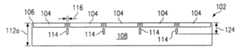
먼저 도 1 및 도 2를 참조하면, 반도체 웨이퍼(2)는 웨이퍼(2)의 상부면(6)에 로우 및 컬럼으로 위치된 복수의 다이 영역(4)을 갖는 기판(3)을 포함하는 것으로 도시된다. 다이 영역(4)은, 공지된 실행방법에 따라 상부면상 및 웨이퍼(2)내에 개별적인 전기적 부품 및 회로가 형성되는 일반적으로 사각형인 경계(8)를 갖는 것으로 도시되며, 여기서 다이 영역들은 약 100㎛ 이상인 것이 보통인 간격(10 및 12)에 의해 수직 및 수평으로 이격되어 있다. 스크라이브 라인 또는 채널(14)이 간격(10 및 12) 안으로 소우 절단되어 웨이퍼(2)로부터 각각의 다이(4)를 분리시킨다. 스크라이브 라인(14)은 종래의 소우 블레이드(도시하지 않음)의 폭으로 인해 25㎛ 이상의 폭(16)을 갖는 것이 보통이다. 도시된 웨이퍼(2)에서, 다이 영역(4)은, 예를 들면, 약 2000㎛의 길이(18) 및 약 1000㎛의 폭(20)을 갖는 하드 디스크 드라이브 프리앰프 회로와 같은 작은 COS 회로를 제조하는데 이용된다. 후속하는 다이 분리를 위하여 웨이퍼 공정기술을 이용하여 이런 크기의 장치들이 제조되는 경우, 다이 영역(4) 사이의 비교적 큰 간격(10 및 12)으로 인해 최적 웨이퍼 공간 이용에 못미치게 된다.Referring first to FIGS. 1 and 2, the
이제 도 3를 참조하면, 본 발명에 따른 또 다른 웨이퍼(52)의 일 부분이 도시되는데, 여기서 다이 영역(54)은 도 1 및 2의 다이 영역(4)과 유사하게, 약 2000㎛의 길이(68) 및 약 1000㎛의 폭(70)을 갖는 경계(58)에 의해 도시된다. 그러나, 도 1 및 2의 웨이퍼(2)와 달리, 본 발명은 약 15㎛ 정도로 작은 폭(56)을 갖는 좁은 채널(64)을 제공함으로써 향상된 웨이퍼 공간 이용을 용이하게 한다. 좁은 채널(64)은, 이웃하는 다이 영역(54)간에 더 작은 간격(60 및 62)을 허용함으로써 웨이퍼(52)에서, 종래의 소우 절단 또는 다른 기계적 다이 분리 기술을 사용하여 가능했던 것보다 향상된 웨이퍼 이용을 용이하게 한다. 예를 들면, 간격(60 및 62)은 약 50㎛ 이하일 수 있으며 일 실시예에서는 약 15㎛ 정도로 작게될 수도 있다.Referring now to FIG. 3, a portion of another
본 발명의 일 측면에 따르면, 다이 영역(54) 사이에서 상부면(56)으로부터 하부면(도시하지 않음)을 향하여 웨이퍼(52) 속으로 채널(64)이 확장하며, 건식 화학 에칭으로 형성된다. 예를 들면, 본 발명의 일 실시예는 최대로 약 15:1 의 가로세로비(예를 들면 깊이 대 폭)로 약 15㎛ 이상인 폭을 갖는 채널을 생성하기 위하여 반응성 이온 에칭(RIE)과 같은 지향성 플라즈마 에칭을 이용하여 상부면(56) 으로부터 재료를 제거하여 채널(64)을 형성하는 단계를 제공한다. 도시된 웨이퍼(52)에서, 채널(64)은 약 130㎛ 이상 약 200㎛ 이하의 깊이를 갖는다. RIE 기술은 이방성인 이온 어시스트 에칭(ion assisted etching)을 포함하며, 상기 에칭은 지향성이다. RIE는 에칭된 표면상의 반응분자들의 화학적 흡수, 표면상으로의 이온의 충돌, 및 표면으로부터의 반응 부산물의 물리적 분리를 포함하며, 그 결과 이방성 지향성 에칭이 발생한다.According to one aspect of the present invention, the
에칭 공정은 포토리소그래픽 기술을 이용할 수 있으며, 그에 따라 종래의 기계적 소우 절단 스크라이브 라인 접근방법에 내재된 정렬 부정확성이 방지되거나 완화되므로, 간격(60 및/또는 62)이 채널폭(56)에 접근하도록 한다. 또한, 채널(64)의 에칭은 기계적 소잉을 통하여 이전에 가능한 것보다 더 좁은 채널폭(56)을 제공할 수 있다. 예를 들면, 현재의 소우 폭은 25㎛ 이상인 반면, 에칭은 약 15㎛ 이하 정도로 좁은 채널폭을 만들 수 있는 것으로 밝혀졌다. 더욱이, 본 발명에 따른 채널 에칭은 소우 절단에 내재된 미립자 생성, 크랙 개시 지점 및 다른 연관된 문제들을 완화시키거나 방지한다.Etching processes may utilize photolithographic techniques, thereby preventing or mitigating alignment inaccuracies inherent in conventional mechanical saw cutting scribe line approaches, so that
이제 도 4-9를 참조하면, 본 발명에 따른 채널 에칭의 일 실시예가 도시된다. 도 4-9에서, 양호한 웨이퍼(102)는 웨이퍼(102)에서 약 50㎛ 이하이며, 본 발명에 따라서 약 15㎛ 정도로 낮게 될 수 있는 간격(110)에 의해 서로 이격되어 있는 다이 영역(104)을 포함한다. 따라서, 100㎛ 이상의 종래의 간격(예를 들면, 도 2의 10 및 12)과는 대조적으로, 본 발명은 다이 간격이 90㎛ 이하로 되게 이용될 수 있다. 도 4에 도시된 바와 같이, 웨이퍼(102)는 약 450 내지 550㎛의 초기 두 께(112)로 상부면(106) 및 하부면(108)을 포함한다. 다이 영역(104)은 공지된 반도체 제조기술로 영역(104)에 형성되고, 이후에 도시되고 설명되는 동작 이전에 테스트될 수 있는 전기 회로 또는 장치(도시하지 않음)를 포함한다. 그 후, 웨이퍼(102)의 하부면(108)은, 기계 연삭(mechanical grinding), 에칭 또는 화학 기계 연마(CMP) 공정을 포함할 수 있는 초기 후면 연삭(back-grind) 공정(120)을 거친다.Referring now to Figures 4-9, one embodiment of a channel etch in accordance with the present invention is shown. 4-9, the
이제 도 5 및 6를 참조하면, 후면 연삭 동작(120)으로 약 150-250㎛ 두께(112a)의 중간 웨이퍼를 생성한다. 그 후, 웨이퍼(102)는 반응성 이온 에칭(RIE)과 같은 지향성 건식에칭 공정(122)을 거쳐서 다이 영역(104) 사이의 간격(110)의 상부면(106)으로부터 재료를 제거한다. 반응성 이온 에칭(122)은 약 15㎛ 정도로 작은 폭(116)을 갖는 채널(114)을 형성하는데, 채널(114)은 상부면(116)으로부터 하부면(108)으로 향하여 아래로 확장하여, 예를 들면 약 130㎛의 깊이(124)에 도달한다. 따라서, 소우 절단의 이용시 통상적인 미립자들을 생성하지 않고 각각의 다이 영역(104) 사이의 웨이퍼(102)에 채널(114)이 생성된다. 더욱이, 에칭 공정(122)은 기계적(예를 들면, 소잉) 기술의 경우보다 정렬 정확성 문제가 상당히 감소된다. 도 4의 초기 후면 연삭 공정(120)은 대안적으로, 예를 들면, 공정(120)의 재료 제거가 심각한 웨이퍼 파손을 야기시키지 않는 에칭 공정(122)을 통하여 채널(114)의 형성에 후속하여 수행될 수 있다.Referring now to FIGS. 5 and 6, back grinding
도 7에 도시된 바와 같이, 회로보드, 서스펜션, 플렉스 회로, 등과 같은 다른 회로와 다이 영역(104)의 회로 사이의 전기적 접속을 제공하기 위하여, 공지된 웨이퍼 범핑기술을 이용해서 골드 스터드 범프(gold stud bump)와 같은 하나 이상의 범프(130)가 다이 영역(104)의 상부면(106)에 도포된다. 그 후, 도 8의 웨이퍼(102)의 상부면(106)에 테이프(132)가 부가되는데, 테이프(132)는 캐리어층(134) 및 접착층(136)을 포함한다. 테이프(132)는 이후에 더 상세히 도시되고 설명되는 바와 같이, 후속하는 다이 분리 동작시 각각의 다이 영역(104)의 상대적 위치를 고정한다.As shown in FIG. 7, gold stud bumps may be employed using known wafer bumping techniques to provide electrical connections between other circuits such as circuit boards, suspensions, flex circuits, and the like, and circuits in
그 후, 웨이퍼(102)는 후면 연삭 동작(140)을 거쳐서 하부면(108)으로부터 재료를 더 제거하여, 도 9에 도시된 바와 같이 약 125㎛의 최종 웨이퍼 두께(112b)를 야기시킨다. 공정(140)은 연삭 또는 에칭과 같은 반도체 장치에 적절한 재료 제거 동작의 한 형태일 수 있으며, 그로 인해 채널(114)이 하부면(108)을 통하여 노출되어(예를 들면, 최종적인 웨이퍼 두께(112b)는 원래의 채널깊이(124)보다 더 작음), 각각의 다이를 분리 또는 개별화한다. 그 후, 각각의 다이는 와이어 본딩을 이용하여 집적 회로(IC)칩 패키지내로 조립될 수 있거나, 초음파 부착기술을 이용하여 회로보드, 서스펜션, 등에 직접 설치될 수 있다.Thereafter,
이제 도 10-23를 참조하면, 본 발명의 또 다른 측면은 반도체 다이 또는 웨이퍼상에 등고 하부면 또는 후면을 생성하는 단계를 포함하는데, 이는 기계적인 재료 제거 기술(예를 들면, 연삭, 절단, 등) 또는 에칭 동작을 통하여 수행될 수 있다. 특히, 선택적 에칭을 사용하는 것은 미립자 생성 및 기계적 기술에 연관된 문제를 완화시키면서 그런 등고 하부면을 제공한다. 등고 하부 웨이퍼면은 매끄러운 표면보다 더 양호한 대류 냉각을 제공하여, 서스펜션(COS), 및 다른 플립칩 형태의 조립품상에 다이가 직접 장착되는 하드 디스크 드라이브 프리앰프 부스터 펌프(booster pump)와 같은 응용에서 회로성능을 향상시킨다.Referring now to FIGS. 10-23, another aspect of the present invention includes creating a contoured bottom or back surface on a semiconductor die or wafer, which may include mechanical material removal techniques (eg, grinding, cutting, Etc.) or through an etching operation. In particular, using selective etching provides such a contoured bottom surface while mitigating problems associated with particulate generation and mechanical techniques. The lower contour wafer surface provides better convection cooling than a smooth surface, such as in hard disk drive preamp booster pumps where the die is mounted directly on suspension (COS) and other flip chip-like assemblies. Improve circuit performance.
또한, 등고 하부면의 에칭은 웨이퍼로부터 각각의 다이를 분리하는데 이용될 수 있으며, 예를 들면, 하부면 에칭은 이웃하는 다이 영역 사이에서 상부면 채널을 노출시킨다. 또한, 서스펜션(또는, 예를 들면, 다른 회로보드)상에 다이를 장착하기 위한 초음파 다이부착 툴링(tooling)시 짝을 이루는 등고면이 제공될 수 있는데, 등고면의 맞물림은 툴링과 다이 사이의 미끄러짐, 및 그와 연관된 미립자 생성을 완화시킨다. 더욱이, 문제가 되는 미립자들이 실질적으로 없는 다이 생성 및 분리를 제공하기 위하여, 전술된 에칭채널과 함께 등고 하부면이 제공될 수 있다.Also, etching of the contour bottom surface can be used to separate each die from the wafer, for example, bottom etching exposes the top channel between neighboring die regions. In addition, paired contours may be provided during ultrasonic die attach tooling for mounting the die on a suspension (or other circuit board, for example), wherein the engagement of the contours between the tooling and the die Mitigates slippage and associated particulate production. Moreover, a contour bottom surface may be provided with the etch channel described above to provide die creation and separation substantially free of problematic particulates.
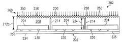
도 10에서, 양호한 웨이퍼(202)의 일 부분이 도시되며, 이것은 도 7 및 8의 웨이퍼(102)와 구조상 유사하다. 웨이퍼(202)는 상부 또는 전면(206)에서 그 내부에 형성된 전기 회로 및/또는 부품(도시하지 않음)을 갖는 복수의 다이 영역(204)을 포함한다. 이웃하는 다이 영역(204) 사이에서 상부면(206)으로부터 하부 또는 후면(208)을 향하여 확장하는 채널(214)이 제공되는데, 채널(214)은 웨이퍼(202)의 초기 두께(212a)보다 작은 깊이(224)(예를 들면, 약 130 내지 150㎛)를 갖는다. 채널(214)은 반응성 이온 에칭(RIE)과 같은 지향성 건식에칭 공정을 이용하여 전술된 바와 같이 에칭되거나 임의의 적절한 기술에 의해 제공될 수 있다.In FIG. 10, a portion of the
그러나, 전술된 바와 같이, 채널(214)을 에칭하는 단계는 종래의 소우 절단 방법론에 비하여 제조공정시 미립자 생성의 완화를 제공하는 것을 이해할 것이다. 다이 영역(204)의 회로에 대한 전기적 상호접속을 제공하기 위하여, 다이 영역(204)의 상부면(206)상에 골드 스터드 범프(230)와 같은 범프가 제공된다. 다이 분리 이후에 각각의 다이가 서로에 대한 공간적인 관계에 있어서 유지되도록, 스터드 범프(230) 및 다이 영역(204)을 캐리어층(234) 및 접착층(236)으로 커버하는 테이프(232)가 상부면(206)상에 장착된다.However, as described above, it will be appreciated that etching the
도 10에 도시된 바와 같이, 초기 하부면 에칭 동작(240)이 하부면(208)상에서 수행되어 도 11에 도시된 바와 같이 웨이퍼 두께(212b)를 제공한다. 그 후, 도 12에서 도시된 바와 같이, 도트(250)의 패턴이 하부면(208)에 도포되는데, 도트(250)는 통상적으로는 웨이퍼(202)보다 더 낮은 에칭속도를 갖는 재료를 포함한다. 예를 들면, 도트는 원하는 등고 하부면에 따른 임의의 적절한 패턴 및 형상으로 하부면(208)상에 분사되는 폴리머 재료일 수 있다. 이 시점에서 웨이퍼(202)보다 더 낮을(그러나 반드시는 아님) 수 있는 에칭속도를 갖는 임의의 적절한 항에칭 재료가 이용될 수 있으며, 선택적 에칭으로 인한 등고면은 그 에칭속도 및 두께의 조합으로부터 생성되는 것을 주목한다. 예를 들면, 도트 재료(250)가 실리콘 웨이퍼(202)상에서 원하는 에칭에 비하여 매우 두꺼운 경우, 더 빠른 에칭속도를 갖는 재료가 도트(250)로 이용될 수 있다. 또한, 도 23a 및 23b를 참조하면, 도트(250)는 원형이고, 도시된 실시예에서 약 25㎛인 간격 또는 피치(252)로 하부면(208)상에 로우와 컬럼 패턴으로 배치될 수 있다. 본 발명에 따른 임의의 적절한 패턴 및 형상이 이용될 수 있으므로, 하부면(208)의 선택적 에칭은 여기에서 도시되고 설명된 것들 이외의 패턴, 간격, 도트 크기 및 형상을 포함하는 등고 하부면(280)을 생성할 수 있다.As shown in FIG. 10, an initial bottom
도트(250)의 패턴이 도포되면(예를 들면 분사 또는 포토리소그래픽 기술을 통함), 도 13-15에 도시된 바와 같이 하부면(208)상에서 에칭 동작(260)이 수행되며, 웨이퍼 두께는 각각 도 13-15에서 도시된 바와 같이, 212b(도 12)로부터 212c, 212d, 및 최종적으로 212e로 점차 감소된다. 웨이퍼(202)의 기판 재료(예를 들면, 실리콘)의 에칭 속도, 및 도트(250)의 에칭 속도와 형상의 조합은 동작(260)을 통한 희생 에칭(sacrificial etching)으로 하부면(208)을 등고화하는 것을 제공하며, 최종적인 웨이퍼 두께(212e)에 도달하면 도트(250)는 완전히 에칭되고, 최종적인 두께(212e)는 원래의 채널깊이(224)보다 더 작게 된다. 이런 방식으로, 선택적 에칭 공정(260)은 하부면(208)상에 높이(284) 및 간격(252)의 등고 볼록 형상(282)을 갖는 등고면(280)을 제공함과 동시에 채널(214)을 노출시켜서, 도 15 및 16에서 도시된 바와 같이 개별적인 다이(270, 272, 274)를 서로 분리시킨다.Once the pattern of
따라서, 하부면(208)상에 상이한 등고면(280)을 다양하게 제공하기 위하여, 도트(250)의 에칭속도, 및 선택적 에칭(260)과 연관된 공정 파라미터뿐만 아니라, 도트(250)의 패턴(예를 들면, 크기, 형상, 간격, 패턴, 두께, 프로파일, 등)이 선택될 수 있다. 도 20-22를 간략히 참조하면, 본 발명에 따라, 각각 볼록 등고 특성이나 형상(282a, 282b, 및 282c)을 갖는 도 20-22의 표면(280a, 280b, 280c)을 포함하는(그러나 이에 국한하지는 않음) 많은 상이한 등고면(280)이 제공될 수 있다. 예를 들면, 형상(282)은 원뿔형상, 반원형, 또는 임의의 다른 볼록 형상을 포함할 수 있다.Thus, in order to provide a variety of
또한, 등고면(280)은 다양한 패턴, 간격, 피치 등의 등고형상(282)을 포함할 수 있어, 소정의 반도체 다이 생산을 위한 특정의 설계목적에 따라 어셈블리 툴링과의 접속 및 대류 냉각이 이루어질 수 있음을 이해할 것이다. 이에 관하여는, 예를 들면, 대류 냉각에 관한 표면영역을 최대화시키고/거나, 기류저항 및 연관된 진동효과(예를 들면, 회전 디스크 매체에 근접한 기류가 하나 이상의 시스템 부품의 진동을 야기시킬 수 있는(프리앰프 부스터 펌프 회로 다이의 등고면(280)을 이용하여 감소될 수 있음) 하드 디스크 드라이브 응용의 경우)를 최소화시키는 것과 같이, 하나 이상의 설계기준에 따라서, 등고 볼록 형상 및 패터닝이 선택될 수 있다.In addition, the
에칭 공정(260)은 임의의 상용 화학적 건식에칭 공정일 수 있으며, 이에 따라 원하는 최종적인 등고를 이루기 위하여 도트(250)의 패턴 및 에칭 공정(260)이 제어될 수 있다. 더욱이, 다이(270, 272, 및 274)에서 크랙을 감소시키고 스트레스 포인트를 완화시키기 위하여, 노출된 채널(214)의 에지상에서 반경 또는 경사(radius or bevel)를 제공하도록, 채널(214)의 초기 노출 이후에 공정(260)이 계속될 수 있다. 더욱이, 에칭 공정(260)은 무지향성(non-directional) 에칭 동작일 수 있으며, 그로 인해 웨이퍼(202)의 재료 및 작은 방울 또는 도트(250)의 희생적 제거에 의해 하부면(208)의 등고화가 용이해질 수 있다. 이 시점에서, 웨이퍼(202)가 도트(250)를 통한 하부면(208)의 선택적 에칭 및 에칭 동작(260)을 통해 등고화되는 것으로 도시되지만, 본 발명에 따른 다른 수단을 통하여 하부면(208)상에 등고면(280)이 제공될 수 있다. 예를 들면, 본 발명에 따라, 등고면(280)이 하부면(208) 내부로 연삭되어 대류 냉각의 향상, 및 초음파 툴링과의 접속을 제공한다.
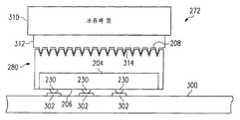
도 16에서 도시된 바와 같이, 최종적으로 원하는 다이 두께(212e)가 달성되고, 채널(214)이 웨이퍼(202)의 후면 또는 하부면(208)으로부터 적절하게 노출되면, 리드 프레임(도시하지 않음)을 갖는 집적 회로 패키지내로 또는 회로 보드, 캐리어, 서스펜션, 또는 다른 회로상으로 직접 조립되기 위하여 도 17의 화살표 방향(290)으로 선택 배치 툴(pick and place tool)에 의해 각각의 반도체 다이(272)가 테이프(232)로부터 제거될 수 있다. 도 18에 도시된 바와 같이, 보드(300)상의 대응하는 본딩 패드(302)와 스터드 범프(230)가 정렬되어, 다이(272)가 회로보드(300)상에 위치된다.As shown in FIG. 16, once the desired
또한 도 19를 참조하면, 초음파 어셈블리 툴(310)은 등고 접속면(314)을 갖는 등고 접속(312)을 이용하여 다이(272)의 하부면(208)과 맞물리게 되는데, 표면(314)은 다이(272)의 등고 하부면(280)과 조합되어 서로 맞물린다. 그 후, 초음파 에너지가 툴(310)로부터 다이(272)로 전달되어 다이(272)의 스터드 범프(230)가 보드(300)의 패드(302)와 기계적 및 전기적으로 접속되도록 작용할 수 있다. 등고면들(314 및 280)의 맞물림은 본 발명의 본 측면에 따라 보드(300)에 다이(272)를 부착하는 동안 미립자 생성을 완화시키고, 또한 다이(272)의 등고 하부면(280)은 보드(300)상에 조립된 다이(272)를 위한 향상된 대류 냉각 성능을 제공할 수 있다.Referring also to FIG. 19, the
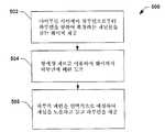
본 발명의 또 다른 측면은 웨이퍼 다이를 생산 및 분리하기 위한 방법들을 제공한다. 본 발명에 따른 양호한 다이 분리 방법(400)이 도 24에 도시된다. 상기 양호한 방법(400), 및 본 발명의 다른 방법들이 이후에 일련의 작용 또는 결과 로서 도시되고 설명되지만, 본 발명은 그런 작용이나 결과의 예시된 순서에 의해 제한되는 것이 아니며, 그 이유는 본 발명에 따라, 어떤 작용들은 상이한 순서로 그리고/또는 여기에서 도시 및/또는 설명된 것들 이외의 다른 작용이나 결과와 동시에 발생할 수 있기 때문이다. 또한, 도시된 모든 단계들이 본 발명에 따른 방법론을 실행하도록 요구될 수 있는 것은 아니다. 더욱이, 방법(400) 및 본 발명의 다른 방법들은 여기에서 도시되고 설명된 장치 및 시스템과 도시되지 않은 다른 시스템과 함께 실행될 수 있다.Another aspect of the invention provides methods for producing and separating a wafer die. A preferred
402에서, 웨이퍼는 상부 및 하부면이 제공되며, 404에서 웨이퍼의 각각의 다이 영역에는 전기 회로가 생성된다. 회로는, 웨이퍼에 전기적 장치들(예를 들면, 트랜지스터, 저항, 커패시터, 및 접속)을 형성시킬 수 있는, 포토리소그래피, 증착, 에칭, 이온주입, 등과 같은 공지된 반도체 웨이퍼 공정 제조기술을 이용하여 생성될 수 있다. 406에서, 이웃하는 다이 영역들 사이의 웨이퍼 상부면에 채널이 에칭된다. 406에서 에칭된 채널은, 건식 화학 에칭 공정을 이용하여 웨이퍼의 상부면으로부터 재료를 제거함으로써, 상부면으로부터 하부면을 향하여 웨이퍼내로 확장한다. 예를 들면, 일 실시예에서는 반응성 이온 에칭(RIE)과 같은 지향성 플라즈마 에칭 공정이 406에서 이용되어 폭은 약 15㎛ 이상이고, 깊이는 약 130㎛ 이상 약 200㎛ 이하인 채널을 생성할 수 있다.At 402, the wafer is provided with top and bottom surfaces, and at 404 an electrical circuit is created in each die region of the wafer. The circuit uses known semiconductor wafer process fabrication techniques such as photolithography, deposition, etching, ion implantation, and the like, which can form electrical devices (eg, transistors, resistors, capacitors, and connections) on the wafer. Can be generated. At 406, the channel is etched into the wafer top surface between neighboring die regions. The channel etched at 406 extends into the wafer from the top surface to the bottom surface by removing material from the top surface of the wafer using a dry chemical etching process. For example, in one embodiment, a directional plasma etching process, such as reactive ion etching (RIE), may be used at 406 to create a channel having a width of at least about 15 μm and a depth of at least about 130 μm and up to about 200 μm.
그 후, 408에서 웨이퍼의 채널링된 상부면상에 캐리어 테이프가 장착된다. 테이프는 후속하는 다이 분리동안 웨이퍼내의 각각의 다이의 서로에 대한 상대적 위치를 고정한다. 또한, 다이 영역이 상부면상에 범프(예를 들면, 골드 스터드 범 프 또는 다른 형태의 범프)를 가지는 경우, 테이프는 후속하는 처리동안 범프의 보호 및 기계적 지지를 제공한다. 그 후 410에서, 각각의 다이를 분리하거나 개별화하도록 웨이퍼의 하부 또는 후면으로부터 재료가 제거된다. 예를 들면, 410에서 재료의 제거는 상부면 채널을 노출시켜서 이웃하는 다이를 서로 분리시키는 단계를 포함할 수 있다. 그 후, 다이는 회로나 집적 회로 패키지로의 조립을 위하여 테이프로부터 제거될 수 있다. 더욱이, 410에서 하부면 재료의 제거는, 에칭, 연삭, 등과 같은 임의의 적절한 기술에 의해 이루어질 수 있다. 406에서 채널의 에칭은 종래의 소우 절단된 채널에 의해 생성된 미립자 물질의 방지 또는 완화를 제공하고, 410에서 재료의 제거는 동일한 문제를 방지하거나 완화하기 위하여 에칭 기술을 이용하여 수행될 수 있다.The carrier tape is then mounted on the channeled top surface of the wafer at 408. The tape fixes the relative position of each die within the wafer relative to each other during subsequent die separation. In addition, where the die area has bumps (eg gold stud bumps or other types of bumps) on the top surface, the tape provides protection and mechanical support of the bumps during subsequent processing. Then at 410, material is removed from the bottom or back side of the wafer to separate or individualize each die. For example, removal of material at 410 may include exposing the top surface channels to separate neighboring dies from each other. The die may then be removed from the tape for assembly into a circuit or integrated circuit package. Moreover, removal of the bottom surface material at 410 may be accomplished by any suitable technique, such as etching, grinding, and the like. Etching the channel at 406 provides prevention or mitigation of particulate material produced by the conventional saw cut channel, and removal of material at 410 can be performed using an etching technique to prevent or mitigate the same problem.
본 발명의 또 다른 측면은 다이 또는 웨이퍼상의 등고 하부면의 생성을 포함한다. 등고면은 동작시 다이로부터 발생하는 열의 효과적이거나 향상된 대류를 제공하고, 미립자 생성을 완화시키기 위하여 초음파 및 다른 조립 툴링에 대하여 미끄러지는 정도가 낮은 접속을 더 제공할 수 있다. 이제 도 25를 참조하면, 웨이퍼 다이를 분리하기 위한 또 다른 양호한 방법(500)이 도시되며, 이웃하는 다이 부분들 사이에서 그 상부면으로부터 하부면으로 확장하는 채널을 갖는 웨이퍼가 502에서 제공된다. 전술된 지향성 에칭 기술, 소우 절단, 또는 다른 방법론의 이용을 포함하는 임의의 적절한 방식으로 채널이 형성될 수 있다. 504에서, 항에칭 재료를 이용하여 웨이퍼의 하부면으로 일 패턴이 도포된다. 하부면상에 분사될 수 있는 폴리머와 같은 임의의 재료가 이용될 수 있으며, 상기 폴리머의 에칭속도는 반 도체 웨이퍼의 경우보다 더 낮다. 더욱이, 폴리머는 임의의 원하는 패턴에 따라 도포될 수 있고, 재료는 임의의 크기 및/또는 형상의 작은 방울로 도포될 수 있다.Another aspect of the invention involves the creation of a contoured bottom surface on a die or wafer. The contour surface may provide an effective or improved convection of heat generated from the die during operation, and may further provide a low slip connection for ultrasonic and other assembly tooling to mitigate particulate generation. Referring now to FIG. 25, another
506에서, 하부면은 패턴에 따라 선택적으로 에칭되어 웨이퍼의 하부면의 전부 또는 일 부분상에 등고 하부면을 제공한다. 하부면 에칭은 506에서 웨이퍼 다이를 서로 분리시키기 위하여 채널을 더 노출시킬 수 있다. 506에서 웨이퍼의 하부면의 선택적 에칭은 플라즈마를 사용하여 수행되어 등고면을 생성할 수 있는데, 예를 들면, 무지향성 플라즈마 에칭은, 웨이퍼 하부상에 등고 볼록 특성 또는 형상을 생성하기 위하여 폴리머 방울들의 패턴으로부터 뿐만 아니라 웨이퍼 하부면으로부터 재료를 희생적으로 제거한다. 예를 들면, 웨이퍼 후면상에 반구형의 볼록 형상을 제공하기 위하여, 원형의 폴리머 방울들의 그리드 패턴이 무지향성 플라즈마 에칭과 함께 이용될 수 있다. 그 후, 이 형상들이 이용되어 조립동안 초음파 툴링과 접속할 뿐만 아니라, 다이 회로의 동작동안 향상된 대류 냉각을 제공할 수 있다. 본 발명에 따른 임의의 형상 및 패턴이 이용될 수 있으며, 그에 따라 그러한 장점들이 달성될 수 있다. 본 발명의 다양한 측면의 추가적인 장점은, 범핑되고 전면에칭된 등고 후면의 다이가 필름 캐리어상에 여전히 있는 상태에서 포장되거나 선적될 수 있으므로, 골드 스터드 범프를 취급손상으로부터 보호한다는 점이다.At 506, the bottom surface is selectively etched according to the pattern to provide a contoured bottom surface on all or a portion of the bottom surface of the wafer. Bottom etching may further expose the channel to separate wafer dies from each other at 506. Selective etching of the bottom surface of the wafer at 506 may be performed using a plasma to produce a contoured surface, for example, an omnidirectional plasma etching may be performed on the polymer droplets to produce contoured convex characteristics or shapes on the bottom of the wafer. Sacrificially remove material from the wafer as well as from the pattern. For example, to provide a hemispherical convex shape on the wafer backside, a grid pattern of circular polymer droplets may be used with omnidirectional plasma etching. These shapes can then be used to connect with ultrasonic tooling during assembly, as well as to provide improved convective cooling during operation of the die circuit. Any shape and pattern according to the present invention can be used and such advantages can be achieved accordingly. An additional advantage of the various aspects of the present invention is that it protects the gold stud bumps from handling damage as the bumped and front etched back die can be packaged or shipped while still on the film carrier.
이제 도 26를 참조하면, 본 발명의 또 다른 측면은 회로보드, 서스펜션(예를 들면 COS 기술을 사용), 기판, 플렉스 회로, 등과 같은 전기 회로로 반도체 다이를 조립하기 위한 기술들을 제공한다. 도 26에는 양호한 방법(600)이 제시되며, 여기서는 602에서 하부면상에 제1 등고면을 갖고 상부면상에 범프(예를 들면 골드 스터 드 범프)를 갖는 다이가 제공된다. 예를 들면, 도 18 및 19의 다이(272)는 상부면(206)상에 스터드 범프(230)를 그리고 하부면(208)상에 등고면(280)을 포함한다. 604에서, 스터드 범프로의 접속을 위한 패드를 갖는 서스펜션(또는, 다른 회로보드)이 제공된다. 본 발명에 따르면, 제2 등고면과의 다이 접속을 갖는, 도 19의 초음파 어셈블리 툴(310)과 같은 어셈블리 툴이 제공된다. 예를 들면 도 19의 접속(312)은 등고면(314)을 포함한다.Referring now to FIG. 26, another aspect of the present invention provides techniques for assembling a semiconductor die into electrical circuits such as circuit boards, suspensions (eg, using COS technology), substrates, flex circuits, and the like. A
608에서, 다이 스터드 범프는 서스펜션 패드와 맞물리고, 610에서 제1 및 제2 등고면들이 맞물린다. 그 후, 스터드 범프가 서스펜션 패드에 고정되도록 하는 등고 접속을 이용하여, 612에서 초음파 툴로부터 다이로 에너지가 전달된다. 다이상의 제1 등고면은, 패터닝된 에칭이 이용된 전술되고 도시된 것들을 포함하는 임의의 적절한 방법론에 의해 제공될 수 있다. 방법(600)은 제1 및 제2 등고면들의 조합된 맞물림을 통하여 초음파 툴과 다이 사이의 미끄러짐을 방지하거나 완화시키면서 서스펜션이나 회로에 다이를 조립한다. 미끄러짐이 감소되는 것은 종래의 초음파 다이 부착에서 전형적인 미립자 생성을 감소 또는 제거한다. 등고 초음파 어셈블리 툴 접속의 사용뿐만 아니라, 다이를 분리하고 등고 하부면을 생성하기 위한 채널 에칭, 하부면 에칭과 같은 본 발명의 다양한 측면들이 결합되어 실질적으로 미립자가 없는 반도체 다이의 제조 및 조립을 제공할 수 있으며, 그로 인해 미립자 물질과 연관된 전술된 문제들이 완화되거나 방지될 수 있다.At 608, the die stud bump is engaged with the suspension pad, and at 610 the first and second contours are engaged. Thereafter, energy is transferred from the ultrasonic tool to the die at 612 using a contour connection that allows the stud bumps to be secured to the suspension pad. The first contour on the die may be provided by any suitable methodology, including those described above and shown in which patterned etching is used. The
본 발명이 하나 이상의 실시예들에 관하여 도시되고 설명되었지만, 당업자들에게는 본 명세서 및 첨부된 도면을 참조하고 이해한 후에는 동등한 변경 및 변형 이 가능할 것이다. 전술된 부품들(조립품, 장치, 회로, 등)에 의해 수행된 다양한 기능들에 관하여, 그런 부품들을 설명하기 위하여 이용된 용어("수단"에 대한 언급을 포함)는, 달리 표시되지 않는 한, 본 발명의 여기서 도시된 양호한 실시예들의 기능을 수행하는 개시된 구조에 구조적으로 동등한 것이 아닐지라도, 설명된 부품의 특정의 기능을 수행하는 임의의 부품에 대응(즉, 기능적으로 동등함)하도록 의도된다. 또한, 본 발명의 특정의 특징이 몇 가지 실시예들중 오직 하나에 관하여 개시되었을지도 모르지만, 그런 특징은, 임의의 주어진 또는 특정의 응용에 바람직하고 유리할 수 있는 것처럼, 다른 실시예들의 하나 이상의 다른 특징들과 결합될 수 있다. 더욱이, 용어 "포함하다", "가지는", "갖다", "구비하는", 또는 그 변형들이 상세한 설명이나 청구범위에서 사용되었다는 점에서, 그런 용어들은 용어 "포함하는"과 유사한 방식으로 포함하려는 의도이다.While the present invention has been shown and described with respect to one or more embodiments, equivalent changes and modifications will become possible to those skilled in the art after referring to and understanding the present specification and the accompanying drawings. With respect to the various functions performed by the aforementioned components (assemblies, devices, circuits, etc.), the terms used to describe such components (including references to "means"), unless otherwise indicated, Although not structurally equivalent to the disclosed structure for carrying out the functions of the preferred embodiments shown herein of the invention, it is intended to correspond to (i.e., functionally equivalent to) any part that performs a particular function of the described part. . In addition, while a particular feature of the present invention may have been disclosed with respect to only one of several embodiments, such a feature may be one or more other of other embodiments, as may be desirable and advantageous for any given or particular application. Can be combined with features. Moreover, the terms "comprise", "having", "have", "having", or variations thereof are used in the description or claims, such terms are intended to be included in a manner similar to the term "comprising". It is intention.
본 발명의 일 측면에 따르면, 반응성 이온 에칭(RIE)과 같은 지향성 에칭 기술을 이용하여, 반도체 웨이퍼의 다이 영역들 사이에 얇은 채널이나 트렌치를 생성하여, 소우 절단시 기계적 정렬의 부정확성을 제공하여 미리 낭비되는 이웃하는 영역들 사이의 여분의 공간을 없앤다. 또한, 에칭된 채널은 소우 블레이드를 이용하여 가능한 것보다 더 좁게 만들어질 수 있다. 또한, 화학에칭을 사용하여 다이들 사이에 채널을 생성하는 것은 이전에 소우 절단 기술에 연관된 미립자 물질을 감소시키거나 완화시킨다.According to one aspect of the invention, using a directional etching technique such as reactive ion etching (RIE), thin channels or trenches are created between die regions of a semiconductor wafer to provide inaccuracies in mechanical alignment during sawing cut in advance. Eliminates extra space between wasted neighboring areas. In addition, the etched channels can be made narrower than possible using saw blades. In addition, creating channels between dies using chemical etching reduces or mitigates particulate material previously associated with saw cutting techniques.
본 발명의 또 다른 측면에 따르면, 웨이퍼의 후면이나 하부면에 등고면을 제 공하는 단계를 포함하며, 건식 화학 에칭이 이용되는 경우, 종래의 후면 연삭에 의해 생성되는 미립자들이 방지될 수 있고, 다이 하부상의 등고면의 제공은 주변의 동작 환경에 더 큰 다이면 영역을 노출시킴으로써, 그 부분의 향상된 대류 냉각을 용이하게 한다. 또한, 등고 하부면은 서스펜션이나 다른 회로보드에 대한 다이의 초음파 부착동안 생성되는 미립자들을 감소시키거나 방지하는데 도움이 될 수 있다.According to another aspect of the present invention, there is provided a contour surface on the back or bottom surface of the wafer, when dry chemical etching is used, fine particles generated by conventional back grinding can be prevented, The provision of a contour surface on the bottom of the die exposes a larger die surface area to the surrounding operating environment, thereby facilitating improved convection cooling of that portion. The contour bottom surface may also help to reduce or prevent particulates generated during ultrasonic attachment of the die to the suspension or other circuit board.
Claims (14)
Translated fromKoreanApplications Claiming Priority (2)
| Application Number | Priority Date | Filing Date | Title |
|---|---|---|---|
| US09/917,534 | 2001-07-27 | ||
| US09/917,534US6686225B2 (en) | 2001-07-27 | 2001-07-27 | Method of separating semiconductor dies from a wafer |
Publications (2)
| Publication Number | Publication Date |
|---|---|
| KR20030010549A KR20030010549A (en) | 2003-02-05 |
| KR100903472B1true KR100903472B1 (en) | 2009-06-18 |
Family
ID=25438928
Family Applications (1)
| Application Number | Title | Priority Date | Filing Date |
|---|---|---|---|
| KR1020020044126AExpired - Fee RelatedKR100903472B1 (en) | 2001-07-27 | 2002-07-26 | Method of separating semiconductor dies from a wafer |
Country Status (4)
| Country | Link |
|---|---|
| US (2) | US6686225B2 (en) |
| JP (1) | JP2003086544A (en) |
| KR (1) | KR100903472B1 (en) |
| TW (1) | TW552676B (en) |
Families Citing this family (86)
| Publication number | Priority date | Publication date | Assignee | Title |
|---|---|---|---|---|
| US6686225B2 (en)* | 2001-07-27 | 2004-02-03 | Texas Instruments Incorporated | Method of separating semiconductor dies from a wafer |
| JP3530158B2 (en)* | 2001-08-21 | 2004-05-24 | 沖電気工業株式会社 | Semiconductor device and manufacturing method thereof |
| DE10245631B4 (en)* | 2002-09-30 | 2022-01-20 | OSRAM Opto Semiconductors Gesellschaft mit beschränkter Haftung | semiconductor device |
| JP2004130579A (en)* | 2002-10-09 | 2004-04-30 | Sony Corp | Liquid discharge head, liquid discharge device, and manufacturing method for liquid discharge head |
| US6897128B2 (en)* | 2002-11-20 | 2005-05-24 | Matsushita Electric Industrial Co., Ltd. | Method of manufacturing semiconductor device, plasma processing apparatus and plasma processing method |
| WO2004053931A2 (en)* | 2002-12-09 | 2004-06-24 | Advanced Interconnect Technologies Limited | Package having exposed integrated circuit device |
| JP3891123B2 (en)* | 2003-02-06 | 2007-03-14 | セイコーエプソン株式会社 | SEMICONDUCTOR DEVICE, ELECTRONIC DEVICE, ELECTRONIC DEVICE, AND SEMICONDUCTOR DEVICE MANUFACTURING METHOD |
| JP4110992B2 (en)* | 2003-02-07 | 2008-07-02 | セイコーエプソン株式会社 | Semiconductor device, electronic device, electronic apparatus, semiconductor device manufacturing method, and electronic device manufacturing method |
| JP4069771B2 (en)* | 2003-03-17 | 2008-04-02 | セイコーエプソン株式会社 | SEMICONDUCTOR DEVICE, ELECTRONIC DEVICE, AND SEMICONDUCTOR DEVICE MANUFACTURING METHOD |
| JP2004281818A (en)* | 2003-03-17 | 2004-10-07 | Seiko Epson Corp | Semiconductor device, electronic device, electronic device, method of manufacturing carrier substrate, method of manufacturing semiconductor device, and method of manufacturing electronic device |
| JP2004281919A (en)* | 2003-03-18 | 2004-10-07 | Seiko Epson Corp | Semiconductor device, electronic device, electronic equipment, method of manufacturing semiconductor device, and method of manufacturing electronic device |
| JP2004281920A (en)* | 2003-03-18 | 2004-10-07 | Seiko Epson Corp | Semiconductor device, electronic device, electronic equipment, method of manufacturing semiconductor device, and method of manufacturing electronic device |
| JP4096774B2 (en)* | 2003-03-24 | 2008-06-04 | セイコーエプソン株式会社 | SEMICONDUCTOR DEVICE, ELECTRONIC DEVICE, ELECTRONIC DEVICE, SEMICONDUCTOR DEVICE MANUFACTURING METHOD, AND ELECTRONIC DEVICE MANUFACTURING METHOD |
| JP2004349495A (en)* | 2003-03-25 | 2004-12-09 | Seiko Epson Corp | Semiconductor device, electronic device, electronic apparatus, and method of manufacturing semiconductor device |
| JP4234630B2 (en)* | 2003-05-29 | 2009-03-04 | 古河電気工業株式会社 | Method of manufacturing thin film circuit board having penetrating structure and protective adhesive tape |
| US7713841B2 (en)* | 2003-09-19 | 2010-05-11 | Micron Technology, Inc. | Methods for thinning semiconductor substrates that employ support structures formed on the substrates |
| US20050064679A1 (en)* | 2003-09-19 | 2005-03-24 | Farnworth Warren M. | Consolidatable composite materials, articles of manufacture formed therefrom, and fabrication methods |
| US20050064683A1 (en)* | 2003-09-19 | 2005-03-24 | Farnworth Warren M. | Method and apparatus for supporting wafers for die singulation and subsequent handling |
| DE10350036B4 (en)* | 2003-10-27 | 2014-01-23 | Robert Bosch Gmbh | Method for separating semiconductor chips and corresponding semiconductor chip arrangement |
| US7244665B2 (en)* | 2004-04-29 | 2007-07-17 | Micron Technology, Inc. | Wafer edge ring structures and methods of formation |
| US7547978B2 (en) | 2004-06-14 | 2009-06-16 | Micron Technology, Inc. | Underfill and encapsulation of semiconductor assemblies with materials having differing properties |
| US7329555B1 (en)* | 2004-07-20 | 2008-02-12 | National Semiconductor Corporation | Method of selectively forming MEMS-based semiconductor devices at the end of a common fabrication process |
| US20060046433A1 (en)* | 2004-08-25 | 2006-03-02 | Sterrett Terry L | Thinning semiconductor wafers |
| US7235431B2 (en) | 2004-09-02 | 2007-06-26 | Micron Technology, Inc. | Methods for packaging a plurality of semiconductor dice using a flowable dielectric material |
| US20060057777A1 (en)* | 2004-09-14 | 2006-03-16 | Howell William C | Separating die on a substrate to reduce backside chipping |
| US7049208B2 (en) | 2004-10-11 | 2006-05-23 | Intel Corporation | Method of manufacturing of thin based substrate |
| US7816182B2 (en)* | 2004-11-30 | 2010-10-19 | Stmicroelectronics Asia Pacific Pte. Ltd. | Simplified multichip packaging and package design |
| JP4731241B2 (en)* | 2005-08-02 | 2011-07-20 | 株式会社ディスコ | Wafer division method |
| DE102005050127B3 (en)* | 2005-10-18 | 2007-05-16 | Infineon Technologies Ag | Method for applying a structure of joining material to the backs of semiconductor chips |
| US7871899B2 (en)* | 2006-01-11 | 2011-01-18 | Amkor Technology, Inc. | Methods of forming back side layers for thinned wafers |
| US7378293B2 (en)* | 2006-03-22 | 2008-05-27 | Texas Instruments Incorporated | MEMS fabrication method |
| CN101415769A (en)* | 2006-03-29 | 2009-04-22 | 国家淀粉及化学投资控股公司 | Radiation solidified rubberized adhesive/sealant |
| US7550778B2 (en) | 2006-05-17 | 2009-06-23 | Innovative Micro Technology | System and method for providing access to an encapsulated device |
| KR100817059B1 (en)* | 2006-09-11 | 2008-03-27 | 삼성전자주식회사 | Thin semiconductor package manufacturing method |
| US20080153265A1 (en)* | 2006-12-21 | 2008-06-26 | Texas Instruments Incorporated | Semiconductor Device Manufactured Using an Etch to Separate Wafer into Dies and Increase Device Space on a Wafer |
| US7585750B2 (en)* | 2007-05-04 | 2009-09-08 | Stats Chippac, Ltd. | Semiconductor package having through-hole via on saw streets formed with partial saw |
| KR100863333B1 (en)* | 2007-06-27 | 2008-10-15 | 주식회사 효광 | Substrate processing method and chips manufactured thereby |
| EP2015356A1 (en)* | 2007-07-13 | 2009-01-14 | PVA TePla AG | Method for singulation of wafers |
| US7972902B2 (en) | 2007-07-23 | 2011-07-05 | Samsung Electronics Co., Ltd. | Method of manufacturing a wafer including providing electrical conductors isolated from circuitry |
| KR101185886B1 (en) | 2007-07-23 | 2012-09-25 | 삼성전자주식회사 | Semiconductor chip, semiconductor package, card and system having universal interconnection lines |
| US8859396B2 (en) | 2007-08-07 | 2014-10-14 | Semiconductor Components Industries, Llc | Semiconductor die singulation method |
| US7989319B2 (en)* | 2007-08-07 | 2011-08-02 | Semiconductor Components Industries, Llc | Semiconductor die singulation method |
| US7781310B2 (en) | 2007-08-07 | 2010-08-24 | Semiconductor Components Industries, Llc | Semiconductor die singulation method |
| US8012857B2 (en)* | 2007-08-07 | 2011-09-06 | Semiconductor Components Industries, Llc | Semiconductor die singulation method |
| US7923298B2 (en) | 2007-09-07 | 2011-04-12 | Micron Technology, Inc. | Imager die package and methods of packaging an imager die on a temporary carrier |
| US8257985B2 (en) | 2008-09-25 | 2012-09-04 | Texas Instruments Incorporated | MEMS device and fabrication method |
| US7943489B2 (en)* | 2008-09-25 | 2011-05-17 | Texas Instruments Incorporated | Bonded wafer assembly system and method |
| US7871857B1 (en)* | 2008-09-29 | 2011-01-18 | Integrated Device Technology, Inc. | Methods of forming multi-chip semiconductor substrates |
| JPWO2010061470A1 (en)* | 2008-11-28 | 2012-04-19 | セイコーインスツル株式会社 | Manufacturing method of wafer and package product |
| CN102257612A (en)* | 2008-12-18 | 2011-11-23 | 精工电子有限公司 | Wafer and method for manufacturing package product |
| TWI513668B (en)* | 2009-02-23 | 2015-12-21 | Seiko Instr Inc | Method for manufacturing glass sealed package and glass substrate |
| TW201104736A (en)* | 2009-04-24 | 2011-02-01 | Henkel Corp | Dicing before grinding process for preparation of semiconductor |
| CN102130025B (en)* | 2009-11-16 | 2015-03-11 | 三星电子株式会社 | Wafer, processing method thereof and method for manufacturing semiconductor device |
| US20110175209A1 (en)* | 2010-01-18 | 2011-07-21 | Seddon Michael J | Method of forming an em protected semiconductor die |
| US8384231B2 (en)* | 2010-01-18 | 2013-02-26 | Semiconductor Components Industries, Llc | Method of forming a semiconductor die |
| US9165833B2 (en) | 2010-01-18 | 2015-10-20 | Semiconductor Components Industries, Llc | Method of forming a semiconductor die |
| US9299664B2 (en)* | 2010-01-18 | 2016-03-29 | Semiconductor Components Industries, Llc | Method of forming an EM protected semiconductor die |
| TWI511253B (en)* | 2010-02-12 | 2015-12-01 | Xintec Inc | Chip package |
| US8409926B2 (en) | 2010-03-09 | 2013-04-02 | Stats Chippac, Ltd. | Semiconductor device and method of forming insulating layer around semiconductor die |
| US20130214370A1 (en)* | 2010-05-03 | 2013-08-22 | S3C, Inc. | System and method for minimizing deflection of a membrance of an absolute pressure sensor |
| KR101617600B1 (en) | 2010-06-08 | 2016-05-02 | 헨켈 아이피 앤드 홀딩 게엠베하 | Coating adhesives onto dicing before grinding and micro-fabricated wafers |
| TWI614816B (en)* | 2010-06-22 | 2018-02-11 | 美國亞德諾半導體公司 | Method of etching and singulating a cap wafer |
| WO2012106191A2 (en) | 2011-02-01 | 2012-08-09 | Henkel Corporation | Pre- cut wafer applied underfill film |
| WO2012106223A2 (en) | 2011-02-01 | 2012-08-09 | Henkel Corporation | Pre-cut wafer applied underfill film on dicing tape |
| JP2012186532A (en) | 2011-03-03 | 2012-09-27 | Seiko Instruments Inc | Wafer, package manufacturing method, and piezoelectric vibrator |
| US8802545B2 (en) | 2011-03-14 | 2014-08-12 | Plasma-Therm Llc | Method and apparatus for plasma dicing a semi-conductor wafer |
| US20120273935A1 (en)* | 2011-04-29 | 2012-11-01 | Stefan Martens | Semiconductor Device and Method of Making a Semiconductor Device |
| US8828848B2 (en)* | 2011-12-16 | 2014-09-09 | Taiwan Semiconductor Manufacturing Company, Ltd. | Die structure and method of fabrication thereof |
| US8952413B2 (en) | 2012-03-08 | 2015-02-10 | Micron Technology, Inc. | Etched trenches in bond materials for die singulation, and associated systems and methods |
| US20130256843A1 (en)* | 2012-04-03 | 2013-10-03 | United Microelectronics Corporation | Wafer sawing method and wafer structure beneficial for performing the same |
| KR20140009731A (en)* | 2012-07-12 | 2014-01-23 | 삼성전자주식회사 | Semiconductor chip comprising heat radiation part and method for fabricating the same chip |
| US9484260B2 (en) | 2012-11-07 | 2016-11-01 | Semiconductor Components Industries, Llc | Heated carrier substrate semiconductor die singulation method |
| US9136173B2 (en) | 2012-11-07 | 2015-09-15 | Semiconductor Components Industries, Llc | Singulation method for semiconductor die having a layer of material along one major surface |
| KR102053349B1 (en) | 2013-05-16 | 2019-12-06 | 삼성전자주식회사 | Semiconductor package |
| US9418894B2 (en) | 2014-03-21 | 2016-08-16 | Semiconductor Components Industries, Llc | Electronic die singulation method |
| US9385041B2 (en) | 2014-08-26 | 2016-07-05 | Semiconductor Components Industries, Llc | Method for insulating singulated electronic die |
| SG10201508477VA (en)* | 2014-10-13 | 2016-05-30 | Utac Headquarters Pte Ltd | Methods for singulating semiconductor wafer |
| JP6490459B2 (en)* | 2015-03-13 | 2019-03-27 | 古河電気工業株式会社 | Wafer fixing tape, semiconductor wafer processing method, and semiconductor chip |
| WO2017149689A1 (en)* | 2016-03-02 | 2017-09-08 | 株式会社日立ハイテクノロジーズ | Defect inspection device, pattern chip, and defect inspection method |
| US10366923B2 (en) | 2016-06-02 | 2019-07-30 | Semiconductor Components Industries, Llc | Method of separating electronic devices having a back layer and apparatus |
| CN106024648B (en)* | 2016-06-15 | 2020-02-07 | 华润微电子(重庆)有限公司 | Front and side wall passivation method for discrete device chip |
| JP2018120687A (en)* | 2017-01-24 | 2018-08-02 | 住友電装株式会社 | connector |
| US10373869B2 (en) | 2017-05-24 | 2019-08-06 | Semiconductor Components Industries, Llc | Method of separating a back layer on a substrate using exposure to reduced temperature and related apparatus |
| US10818551B2 (en) | 2019-01-09 | 2020-10-27 | Semiconductor Components Industries, Llc | Plasma die singulation systems and related methods |
| US12315773B2 (en)* | 2022-05-23 | 2025-05-27 | Changzhou Galaxy Century Microelectronics Co., Ltd | Chip scale package (CSP) process |
| CN120179870B (en)* | 2025-05-22 | 2025-08-22 | 杭州开幕光子技术有限公司 | A method for storing test data |
Citations (4)
| Publication number | Priority date | Publication date | Assignee | Title |
|---|---|---|---|---|
| JPH04297056A (en)* | 1991-03-08 | 1992-10-21 | Sony Corp | Manufacture of semiconductor device |
| US5904548A (en)* | 1996-11-21 | 1999-05-18 | Texas Instruments Incorporated | Trench scribe line for decreased chip spacing |
| US5972781A (en)* | 1997-09-30 | 1999-10-26 | Siemens Aktiengesellschaft | Method for producing semiconductor chips |
| JP2001035817A (en)* | 1999-07-22 | 2001-02-09 | Toshiba Corp | Method of dividing wafer and method of manufacturing semiconductor device |
Family Cites Families (22)
| Publication number | Priority date | Publication date | Assignee | Title |
|---|---|---|---|---|
| US3562058A (en) | 1967-05-16 | 1971-02-09 | Texas Instruments Inc | Method for breaking and separating substrate material |
| DE2522346C3 (en)* | 1975-05-20 | 1978-10-26 | Siemens Ag, 1000 Berlin Und 8000 Muenchen | Method for manufacturing semiconductor components |
| KR920004514B1 (en) | 1987-05-01 | 1992-06-08 | 스미도모덴기고오교오 가부시기가이샤 | Semiconductor device manufacturing device |
| US4903089A (en)* | 1988-02-02 | 1990-02-20 | Massachusetts Institute Of Technology | Vertical transistor device fabricated with semiconductor regrowth |
| US5824569A (en)* | 1992-07-15 | 1998-10-20 | Micron Technology, Inc. | Semiconductor device having ball-bonded pads |
| US6184063B1 (en) | 1996-11-26 | 2001-02-06 | Texas Instruments Incorporated | Method and apparatus for breaking and separating a wafer into die using a multi-radii dome |
| US6114187A (en)* | 1997-01-11 | 2000-09-05 | Microfab Technologies, Inc. | Method for preparing a chip scale package and product produced by the method |
| US6127245A (en) | 1997-02-04 | 2000-10-03 | Micron Technology, Inc. | Grinding technique for integrated circuits |
| US5923995A (en)* | 1997-04-18 | 1999-07-13 | National Semiconductor Corporation | Methods and apparatuses for singulation of microelectromechanical systems |
| US5863813A (en)* | 1997-08-20 | 1999-01-26 | Micron Communications, Inc. | Method of processing semiconductive material wafers and method of forming flip chips and semiconductor chips |
| US6087199A (en)* | 1998-02-04 | 2000-07-11 | International Business Machines Corporation | Method for fabricating a very dense chip package |
| US6448184B1 (en)* | 1998-06-25 | 2002-09-10 | Pacific Western Systems | Formation of diamond particle interconnects |
| US6465329B1 (en)* | 1999-01-20 | 2002-10-15 | Amkor Technology, Inc. | Microcircuit die-sawing protector and method |
| US6278181B1 (en)* | 1999-06-28 | 2001-08-21 | Advanced Micro Devices, Inc. | Stacked multi-chip modules using C4 interconnect technology having improved thermal management |
| JP3455762B2 (en)* | 1999-11-11 | 2003-10-14 | カシオ計算機株式会社 | Semiconductor device and manufacturing method thereof |
| JP4409014B2 (en)* | 1999-11-30 | 2010-02-03 | リンテック株式会社 | Manufacturing method of semiconductor device |
| US6184064B1 (en)* | 2000-01-12 | 2001-02-06 | Micron Technology, Inc. | Semiconductor die back side surface and method of fabrication |
| US6717245B1 (en)* | 2000-06-02 | 2004-04-06 | Micron Technology, Inc. | Chip scale packages performed by wafer level processing |
| KR100425934B1 (en)* | 2000-12-29 | 2004-04-03 | 주식회사 하이닉스반도체 | Method of forming a silicon-germanium film |
| US6589809B1 (en)* | 2001-07-16 | 2003-07-08 | Micron Technology, Inc. | Method for attaching semiconductor components to a substrate using local UV curing of dicing tape |
| US6686225B2 (en)* | 2001-07-27 | 2004-02-03 | Texas Instruments Incorporated | Method of separating semiconductor dies from a wafer |
| DE10202881B4 (en)* | 2002-01-25 | 2007-09-20 | Infineon Technologies Ag | Method for producing semiconductor chips with a chip edge protection layer, in particular for wafer level packaging chips |
- 2001
- 2001-07-27USUS09/917,534patent/US6686225B2/ennot_activeExpired - Lifetime
- 2002
- 2002-07-23JPJP2002214138Apatent/JP2003086544A/enactivePending
- 2002-07-26TWTW091116723Apatent/TW552676B/ennot_activeIP Right Cessation
- 2002-07-26KRKR1020020044126Apatent/KR100903472B1/ennot_activeExpired - Fee Related
- 2003
- 2003-12-17USUS10/739,237patent/US20040129451A1/ennot_activeAbandoned
Patent Citations (4)
| Publication number | Priority date | Publication date | Assignee | Title |
|---|---|---|---|---|
| JPH04297056A (en)* | 1991-03-08 | 1992-10-21 | Sony Corp | Manufacture of semiconductor device |
| US5904548A (en)* | 1996-11-21 | 1999-05-18 | Texas Instruments Incorporated | Trench scribe line for decreased chip spacing |
| US5972781A (en)* | 1997-09-30 | 1999-10-26 | Siemens Aktiengesellschaft | Method for producing semiconductor chips |
| JP2001035817A (en)* | 1999-07-22 | 2001-02-09 | Toshiba Corp | Method of dividing wafer and method of manufacturing semiconductor device |
Also Published As
| Publication number | Publication date |
|---|---|
| TW552676B (en) | 2003-09-11 |
| US20040129451A1 (en) | 2004-07-08 |
| US6686225B2 (en) | 2004-02-03 |
| JP2003086544A (en) | 2003-03-20 |
| KR20030010549A (en) | 2003-02-05 |
| US20030022465A1 (en) | 2003-01-30 |
Similar Documents
| Publication | Publication Date | Title |
|---|---|---|
| KR100903472B1 (en) | Method of separating semiconductor dies from a wafer | |
| EP1028463B1 (en) | Method for manufacturing a module with a flexible package having a very thin semiconductor chip | |
| US7138296B2 (en) | Board for manufacturing a BGA and method of manufacturing semiconductor device using thereof | |
| US6541352B2 (en) | Semiconductor die with contoured bottom surface and method for making same | |
| KR100636770B1 (en) | Semiconductor device and method for manufacturing the same | |
| US9666450B2 (en) | Substrate and assembly thereof with dielectric removal for increased post height | |
| JP2003031524A (en) | Semiconductor device and manufacturing method thereof | |
| JP2002368160A (en) | Wafer level package and manufacturing method thereof | |
| JP3618330B2 (en) | Semiconductor device and manufacturing method thereof | |
| JP2004214543A (en) | Semiconductor device and manufacturing method thereof | |
| JP2001338932A (en) | Semiconductor device and method of manufacturing semiconductor device | |
| US8101470B2 (en) | Foil based semiconductor package | |
| JP3880762B2 (en) | Semiconductor device | |
| JP4214969B2 (en) | Manufacturing method of semiconductor device | |
| US6846701B2 (en) | Traceless flip chip assembly and method | |
| SE516748C2 (en) | Flip-chip type assembly connection with elastic contacts for mounting integrated circuits | |
| JP2004119573A (en) | Manufacture of semiconductor device and film sticking apparatus | |
| US20060049520A1 (en) | Semiconductor device mounting structure for reducing thermal stress and warpage | |
| JP2003229381A (en) | Method for manufacturing semiconductor device | |
| JP2004320061A (en) | Semiconductor device and its manufacturing method | |
| CN120109113A (en) | Semiconductor package and method of manufacturing semiconductor package | |
| JP2012199420A (en) | Semiconductor device | |
| JPH04359556A (en) | Method of manufacturing multi-chip-module | |
| JPH05136192A (en) | Mounting method of electronic component | |
| JP2007005382A (en) | Manufacturing method of semiconductor device |
Legal Events
| Date | Code | Title | Description |
|---|---|---|---|
| PA0109 | Patent application | St.27 status event code:A-0-1-A10-A12-nap-PA0109 | |
| PG1501 | Laying open of application | St.27 status event code:A-1-1-Q10-Q12-nap-PG1501 | |
| A201 | Request for examination | ||
| P11-X000 | Amendment of application requested | St.27 status event code:A-2-2-P10-P11-nap-X000 | |
| P13-X000 | Application amended | St.27 status event code:A-2-2-P10-P13-nap-X000 | |
| PA0201 | Request for examination | St.27 status event code:A-1-2-D10-D11-exm-PA0201 | |
| E902 | Notification of reason for refusal | ||
| PE0902 | Notice of grounds for rejection | St.27 status event code:A-1-2-D10-D21-exm-PE0902 | |
| T11-X000 | Administrative time limit extension requested | St.27 status event code:U-3-3-T10-T11-oth-X000 | |
| T11-X000 | Administrative time limit extension requested | St.27 status event code:U-3-3-T10-T11-oth-X000 | |
| T11-X000 | Administrative time limit extension requested | St.27 status event code:U-3-3-T10-T11-oth-X000 | |
| P11-X000 | Amendment of application requested | St.27 status event code:A-2-2-P10-P11-nap-X000 | |
| P13-X000 | Application amended | St.27 status event code:A-2-2-P10-P13-nap-X000 | |
| E90F | Notification of reason for final refusal | ||
| PE0902 | Notice of grounds for rejection | St.27 status event code:A-1-2-D10-D21-exm-PE0902 | |
| T11-X000 | Administrative time limit extension requested | St.27 status event code:U-3-3-T10-T11-oth-X000 | |
| E13-X000 | Pre-grant limitation requested | St.27 status event code:A-2-3-E10-E13-lim-X000 | |
| P11-X000 | Amendment of application requested | St.27 status event code:A-2-2-P10-P11-nap-X000 | |
| P13-X000 | Application amended | St.27 status event code:A-2-2-P10-P13-nap-X000 | |
| E701 | Decision to grant or registration of patent right | ||
| PE0701 | Decision of registration | St.27 status event code:A-1-2-D10-D22-exm-PE0701 | |
| GRNT | Written decision to grant | ||
| PR0701 | Registration of establishment | St.27 status event code:A-2-4-F10-F11-exm-PR0701 | |
| PR1002 | Payment of registration fee | St.27 status event code:A-2-2-U10-U11-oth-PR1002 Fee payment year number:1 | |
| PG1601 | Publication of registration | St.27 status event code:A-4-4-Q10-Q13-nap-PG1601 | |
| PR1001 | Payment of annual fee | St.27 status event code:A-4-4-U10-U11-oth-PR1001 Fee payment year number:4 | |
| FPAY | Annual fee payment | Payment date:20130531 Year of fee payment:5 | |
| PR1001 | Payment of annual fee | St.27 status event code:A-4-4-U10-U11-oth-PR1001 Fee payment year number:5 | |
| FPAY | Annual fee payment | Payment date:20140529 Year of fee payment:6 | |
| PR1001 | Payment of annual fee | St.27 status event code:A-4-4-U10-U11-oth-PR1001 Fee payment year number:6 | |
| PR1001 | Payment of annual fee | St.27 status event code:A-4-4-U10-U11-oth-PR1001 Fee payment year number:7 | |
| FPAY | Annual fee payment | Payment date:20160330 Year of fee payment:8 | |
| PR1001 | Payment of annual fee | St.27 status event code:A-4-4-U10-U11-oth-PR1001 Fee payment year number:8 | |
| FPAY | Annual fee payment | Payment date:20170330 Year of fee payment:9 | |
| PR1001 | Payment of annual fee | St.27 status event code:A-4-4-U10-U11-oth-PR1001 Fee payment year number:9 | |
| FPAY | Annual fee payment | Payment date:20180329 Year of fee payment:10 | |
| PR1001 | Payment of annual fee | St.27 status event code:A-4-4-U10-U11-oth-PR1001 Fee payment year number:10 | |
| FPAY | Annual fee payment | Payment date:20190327 Year of fee payment:11 | |
| PR1001 | Payment of annual fee | St.27 status event code:A-4-4-U10-U11-oth-PR1001 Fee payment year number:11 | |
| R18-X000 | Changes to party contact information recorded | St.27 status event code:A-5-5-R10-R18-oth-X000 | |
| PR1001 | Payment of annual fee | St.27 status event code:A-4-4-U10-U11-oth-PR1001 Fee payment year number:12 | |
| PR1001 | Payment of annual fee | St.27 status event code:A-4-4-U10-U11-oth-PR1001 Fee payment year number:13 | |
| PC1903 | Unpaid annual fee | St.27 status event code:A-4-4-U10-U13-oth-PC1903 Not in force date:20220611 Payment event data comment text:Termination Category : DEFAULT_OF_REGISTRATION_FEE | |
| PC1903 | Unpaid annual fee | St.27 status event code:N-4-6-H10-H13-oth-PC1903 Ip right cessation event data comment text:Termination Category : DEFAULT_OF_REGISTRATION_FEE Not in force date:20220611 |