KR100901236B1 - Image sensor and manufacturing method - Google Patents
Image sensor and manufacturing methodDownload PDFInfo
- Publication number
- KR100901236B1 KR100901236B1KR1020070047589AKR20070047589AKR100901236B1KR 100901236 B1KR100901236 B1KR 100901236B1KR 1020070047589 AKR1020070047589 AKR 1020070047589AKR 20070047589 AKR20070047589 AKR 20070047589AKR 100901236 B1KR100901236 B1KR 100901236B1
- Authority
- KR
- South Korea
- Prior art keywords
- image sensor
- present
- carbon nanotubes
- photodiode
- forming
- Prior art date
- Legal status (The legal status is an assumption and is not a legal conclusion. Google has not performed a legal analysis and makes no representation as to the accuracy of the status listed.)
- Expired - Fee Related
Links
Images


Classifications
- H—ELECTRICITY
- H10—SEMICONDUCTOR DEVICES; ELECTRIC SOLID-STATE DEVICES NOT OTHERWISE PROVIDED FOR
- H10F—INORGANIC SEMICONDUCTOR DEVICES SENSITIVE TO INFRARED RADIATION, LIGHT, ELECTROMAGNETIC RADIATION OF SHORTER WAVELENGTH OR CORPUSCULAR RADIATION
- H10F39/00—Integrated devices, or assemblies of multiple devices, comprising at least one element covered by group H10F30/00, e.g. radiation detectors comprising photodiode arrays
- H10F39/10—Integrated devices
- H10F39/12—Image sensors
- B—PERFORMING OPERATIONS; TRANSPORTING
- B82—NANOTECHNOLOGY
- B82Y—SPECIFIC USES OR APPLICATIONS OF NANOSTRUCTURES; MEASUREMENT OR ANALYSIS OF NANOSTRUCTURES; MANUFACTURE OR TREATMENT OF NANOSTRUCTURES
- B82Y10/00—Nanotechnology for information processing, storage or transmission, e.g. quantum computing or single electron logic
- H—ELECTRICITY
- H10—SEMICONDUCTOR DEVICES; ELECTRIC SOLID-STATE DEVICES NOT OTHERWISE PROVIDED FOR
- H10K—ORGANIC ELECTRIC SOLID-STATE DEVICES
- H10K30/00—Organic devices sensitive to infrared radiation, light, electromagnetic radiation of shorter wavelength or corpuscular radiation
- H10K30/20—Organic devices sensitive to infrared radiation, light, electromagnetic radiation of shorter wavelength or corpuscular radiation comprising organic-organic junctions, e.g. donor-acceptor junctions
- H—ELECTRICITY
- H10—SEMICONDUCTOR DEVICES; ELECTRIC SOLID-STATE DEVICES NOT OTHERWISE PROVIDED FOR
- H10K—ORGANIC ELECTRIC SOLID-STATE DEVICES
- H10K39/00—Integrated devices, or assemblies of multiple devices, comprising at least one organic radiation-sensitive element covered by group H10K30/00
- H10K39/30—Devices controlled by radiation
- H10K39/32—Organic image sensors
- B—PERFORMING OPERATIONS; TRANSPORTING
- B82—NANOTECHNOLOGY
- B82Y—SPECIFIC USES OR APPLICATIONS OF NANOSTRUCTURES; MEASUREMENT OR ANALYSIS OF NANOSTRUCTURES; MANUFACTURE OR TREATMENT OF NANOSTRUCTURES
- B82Y20/00—Nanooptics, e.g. quantum optics or photonic crystals
- H—ELECTRICITY
- H10—SEMICONDUCTOR DEVICES; ELECTRIC SOLID-STATE DEVICES NOT OTHERWISE PROVIDED FOR
- H10F—INORGANIC SEMICONDUCTOR DEVICES SENSITIVE TO INFRARED RADIATION, LIGHT, ELECTROMAGNETIC RADIATION OF SHORTER WAVELENGTH OR CORPUSCULAR RADIATION
- H10F39/00—Integrated devices, or assemblies of multiple devices, comprising at least one element covered by group H10F30/00, e.g. radiation detectors comprising photodiode arrays
- H10F39/80—Constructional details of image sensors
- H10F39/803—Pixels having integrated switching, control, storage or amplification elements
- H—ELECTRICITY
- H10—SEMICONDUCTOR DEVICES; ELECTRIC SOLID-STATE DEVICES NOT OTHERWISE PROVIDED FOR
- H10K—ORGANIC ELECTRIC SOLID-STATE DEVICES
- H10K30/00—Organic devices sensitive to infrared radiation, light, electromagnetic radiation of shorter wavelength or corpuscular radiation
- H10K30/80—Constructional details
- H10K30/81—Electrodes
- H10K30/82—Transparent electrodes, e.g. indium tin oxide [ITO] electrodes
- H10K30/821—Transparent electrodes, e.g. indium tin oxide [ITO] electrodes comprising carbon nanotubes
- H—ELECTRICITY
- H10—SEMICONDUCTOR DEVICES; ELECTRIC SOLID-STATE DEVICES NOT OTHERWISE PROVIDED FOR
- H10K—ORGANIC ELECTRIC SOLID-STATE DEVICES
- H10K85/00—Organic materials used in the body or electrodes of devices covered by this subclass
- H10K85/20—Carbon compounds, e.g. carbon nanotubes or fullerenes
- H10K85/221—Carbon nanotubes
- Y—GENERAL TAGGING OF NEW TECHNOLOGICAL DEVELOPMENTS; GENERAL TAGGING OF CROSS-SECTIONAL TECHNOLOGIES SPANNING OVER SEVERAL SECTIONS OF THE IPC; TECHNICAL SUBJECTS COVERED BY FORMER USPC CROSS-REFERENCE ART COLLECTIONS [XRACs] AND DIGESTS
- Y02—TECHNOLOGIES OR APPLICATIONS FOR MITIGATION OR ADAPTATION AGAINST CLIMATE CHANGE
- Y02E—REDUCTION OF GREENHOUSE GAS [GHG] EMISSIONS, RELATED TO ENERGY GENERATION, TRANSMISSION OR DISTRIBUTION
- Y02E10/00—Energy generation through renewable energy sources
- Y02E10/50—Photovoltaic [PV] energy
- Y02E10/549—Organic PV cells
- Y—GENERAL TAGGING OF NEW TECHNOLOGICAL DEVELOPMENTS; GENERAL TAGGING OF CROSS-SECTIONAL TECHNOLOGIES SPANNING OVER SEVERAL SECTIONS OF THE IPC; TECHNICAL SUBJECTS COVERED BY FORMER USPC CROSS-REFERENCE ART COLLECTIONS [XRACs] AND DIGESTS
- Y02—TECHNOLOGIES OR APPLICATIONS FOR MITIGATION OR ADAPTATION AGAINST CLIMATE CHANGE
- Y02P—CLIMATE CHANGE MITIGATION TECHNOLOGIES IN THE PRODUCTION OR PROCESSING OF GOODS
- Y02P70/00—Climate change mitigation technologies in the production process for final industrial or consumer products
- Y02P70/50—Manufacturing or production processes characterised by the final manufactured product
Landscapes
- Engineering & Computer Science (AREA)
- Physics & Mathematics (AREA)
- Chemical & Material Sciences (AREA)
- Nanotechnology (AREA)
- Electromagnetism (AREA)
- Mathematical Physics (AREA)
- Theoretical Computer Science (AREA)
- Crystallography & Structural Chemistry (AREA)
- Solid State Image Pick-Up Elements (AREA)
- Light Receiving Elements (AREA)
Abstract
Translated fromKoreanDescription
Translated fromKorean도 1은 본 발명의 제1 실시예에 따른 이미지센서의 단면도.1 is a cross-sectional view of an image sensor according to a first embodiment of the present invention.
도 2a 내지 도 2f는 본 발명의 제1 실시예에 따른 이미지센서 제조방법의 공정단면도.2A to 2F are cross-sectional views of a manufacturing method of an image sensor according to a first exemplary embodiment of the present invention.
도 3는 본 발명의 제2 실시예에 따른 이미지센서의 단면도.3 is a sectional view of an image sensor according to a second embodiment of the present invention;
도 4는 본 발명의 제3 실시예에 따른 이미지센서의 단면도.4 is a sectional view of an image sensor according to a third embodiment of the present invention;
도 5는 본 발명의 제4 실시예에 따른 이미지센서의 단면도.5 is a cross-sectional view of an image sensor according to a fourth embodiment of the present invention.
도 6은 본 발명의 제5 실시예에 따른 이미지센서의 단면도.6 is a sectional view of an image sensor according to a fifth embodiment of the present invention;
본 발명의 실시예는 이미지센서 및 그 제조방법에 관한 것이다.An embodiment of the present invention relates to an image sensor and a manufacturing method thereof.
일반적으로, 이미지 센서(Image sensor)는 광학적 영상(optical image)을 전기적 신호로 변환시키는 반도체 소자로써, 크게 전하결합소자(charge coupled device: CCD) 이미지센서와 씨모스(CMOS; Complementary Metal Oxide Silicon) 이미지 센서(Image Sensor)(CIS)로 구분된다.In general, an image sensor is a semiconductor device that converts an optical image into an electrical signal, and is mainly a charge coupled device (CCD) image sensor and a CMOS (Complementary Metal Oxide Silicon) It is divided into an image sensor (CIS).
한편, CCD 이미지센서는 구동 방식이 복잡하고, 전력 소비가 클 뿐만 아니라, 다단계의 포토 공정이 요구되므로 제조 공정이 복잡한 단점이 있으므로, 최근에는 상기 전하 결합 소자의 단점을 극복하기 위한 차세대 이미지 센서로서 씨모스 이미지 센서가 주목을 받고 있다.On the other hand, the CCD image sensor has a complex driving method, a large power consumption, and requires a multi-stage photo process, so that the manufacturing process is complicated. CMOS image sensors are getting attention.
씨모스 이미지센서는 단위 화소 내에 포토다이오드와 모스트랜지스터를 형성시킴으로써 스위칭방식으로 각 단위 화소의 전기적 신호를 순차적으로 검출하여 영상을 구현한다.The CMOS image sensor implements an image by sequentially detecting an electrical signal of each unit pixel by a switching method by forming a photodiode and a MOS transistor in the unit pixel.
종래기술에 의한 씨모스 이미지센서는 빛 신호를 받아서 전기 신호로 바꾸어 주는 포토다이오드(Photo Diode) 영역(미도시)과, 이 전기 신호를 처리하는 트랜지스터 영역(미도시)으로 구분할 수 있다.The CMOS image sensor according to the related art may be divided into a photo diode region (not shown) for receiving a light signal and converting the light signal into an electrical signal, and a transistor region (not shown) for processing the electrical signal.
그런데, 종래기술에 따른 씨모스 이미지센서는 포토다이오드가 트랜지스터와 수평으로 배치되는 구조이다.However, the CMOS image sensor according to the related art has a structure in which a photodiode is horizontally disposed with a transistor.
물론, 종래기술에 의한 수평형의 씨모스 이미지센서에 의해 CCD 이미지센서의 단점이 해결되기는 하였으나, 종래기술에 의한 수평형의 씨모스 이미지센서에는 여전히 문제점들이 있다.Of course, although the disadvantages of the CCD image sensor are solved by the horizontal CMOS image sensor according to the prior art, there are still problems in the horizontal CMOS image sensor according to the prior art.
즉, 종래기술에 의한 수평형의 씨모스 이미지센서에 의하면 포토다이오드와 트랜지스터가 기판상에 상호 수평으로 인접하여 제조된다. 이에 따라, 포토다이오드를 위한 추가적인 영역이 요구되며, 이에 의해 필팩터(fill factor) 영역을 감소시키고 또한 레졀류션(Resolution)의 가능성을 제한하는 문제가 있다.That is, according to the horizontal CMOS image sensor of the prior art, a photodiode and a transistor are manufactured to be adjacent to each other horizontally on a substrate. Accordingly, an additional area for the photodiode is required, thereby reducing the fill factor area and limiting the possibility of resolution.
또한, 종래기술에 의한 수평형의 씨모스 이미지센서에 의하면 포토다이오드 와 트랜지스터를 동시에 제조하는 공정에 대한 최적화를 달성하는 점이 매우 어려운 문제가 있다. 즉, 신속한 트랜지스터 공정에서는 작은 면저항(low sheet resistance)을 위해 샐로우 졍션(shallow junction)이 요구되나, 포토다이오드에는 이러한 샐로우 졍션(shallow junction)이 적절하지 않을 수 있다.In addition, according to the horizontal CMOS image sensor according to the prior art there is a problem that it is very difficult to achieve optimization for the process of manufacturing a photodiode and a transistor at the same time. That is, in a fast transistor process, a shallow junction is required for low sheet resistance, but such shallow junction may not be appropriate for a photodiode.
또한, 종래기술에 의한 수평형의 씨모스 이미지센서에 의하면 추가적인 온칩(on-chip) 기능들이 이미지센서에 부가되면서 단위화소의 크기가 이미지센서의 센서티버티(sensitivity)를 유지하기 위해 증가되거나 또는 포토다이오드를 위한 면적이 픽셀사이즈를 유지하기 위해 감소되야한다. 그런데, 픽셀사이즈가 증가되면 이미지센서의 레졀류션(Resolution)이 감소하게되며, 또한, 포토다이오드의 면적이 감소되면 이미지센서의 센서티버티(sensitivity)가 감소하는 문제가 발생한다.In addition, according to the horizontal CMOS image sensor according to the prior art, the size of the unit pixel is increased to maintain the sensor sensitivity of the image sensor as additional on-chip functions are added to the image sensor. The area for the photodiode must be reduced to maintain the pixel size. However, when the pixel size is increased, the resolution of the image sensor is reduced, and when the area of the photodiode is reduced, the sensor sensitivity of the image sensor is reduced.
본 발명의 실시예는 트랜지스터 회로(circuitry)와 포토다이오드의 새로운 집적을 제공할 수 있는 이미지센서 및 그 제조방법을 제공하고자 한다.An embodiment of the present invention is to provide an image sensor and a method of manufacturing the same that can provide a new integration of a transistor circuit (circuitry) and a photodiode.
또한, 본 발명의 실시예는 양자효율(quantum efficiency)을 높일 수 있는 포토다이오드를 포함하는 이미지센서 및 그 제조방법을 제공하고자 한다.In addition, an embodiment of the present invention is to provide an image sensor and a manufacturing method comprising a photodiode that can increase the quantum efficiency (quantum efficiency).
또한, 본 발명의 실시예는 레졀류션(Resolution)과 센서티버티(sensitivity)가 함께 개선될 수 있는 이미지센서 및 그 제조방법을 제공하고자 한다.In addition, an embodiment of the present invention is to provide an image sensor and a method of manufacturing the same that can be improved together with the resolution (Resolution) and sensor sensitivity (sensitivity).
또한, 본 발명의 실시예는 수직형의 포토다이오드를 채용하면서 포토다이오드 내에 디펙트를 방지할 수 있는 이미지센서 및 그 제조방법을 제공하고자 한다.In addition, an embodiment of the present invention is to provide an image sensor and a manufacturing method thereof that can prevent the defect in the photodiode while employing a vertical photodiode.
본 발명의 실시예에 따른 이미지센서는 기판상에 형성된 씨모스 회로(circuitry); 상기 기판상에 형성된 하부배선; 상기 하부배선 상에 형성된 카본나노튜브; 상기 카본나노튜브에 형성된 전도성 고분자; 및 상기 카본나노튜브 상에 형성된 투명전극;을 포함하는 것을 특징으로 한다.An image sensor according to an embodiment of the present invention includes a CMOS circuit (circuitry) formed on the substrate; A lower wiring formed on the substrate; Carbon nanotubes formed on the lower interconnection; A conductive polymer formed on the carbon nanotubes; And a transparent electrode formed on the carbon nanotubes.
또한, 본 발명의 실시예에 따른 이미지센서의 제조방법은 씨모스 회로(circuitry)를 기판상에 형성하는 단계; 상기 기판상에 하부배선을 형성하는 단계; 상기 하부배선 상에 카본나노튜브를 형성하는 단계; 상기 카본나노튜브에 전도성 고분자를 형성하는 단계; 및 상기 카본나노튜브 상에 투명전극을 형성하는 단계;를 포함하는 것을 특징으로 한다.In addition, the manufacturing method of the image sensor according to an embodiment of the present invention comprises the steps of forming a CMOS circuit (circuitry) on the substrate; Forming a lower wiring on the substrate; Forming carbon nanotubes on the lower interconnections; Forming a conductive polymer on the carbon nanotubes; And forming a transparent electrode on the carbon nanotubes.
이와 같은 본 발명의 실시예에 의하면 트랜지스터 회로(circuitry)와 포토다이오드의 수직형 집적을 이룰 수 있고, 또한, 본 발명의 실시예에 의하면 카본나노튜브를 이용해 포토다이오드를 형성함으로써 양자효율(quantum efficiency)을 높일 수 있으며, 또한 본 발명의 실시예는 포토다이오드 내에 디펙트를 방지함으로써 필팩터(fill factor) 및 센서티버티(sensitivity) 등의 향상과 소자의 소형화 및 제조비용을 절감을 획득할 수 있는 장점이 있다.According to the embodiment of the present invention, the vertical integration of the transistor circuit and the photodiode can be achieved. Also, according to the embodiment of the present invention, the photodiode is formed using carbon nanotubes to form quantum efficiency. In addition, the embodiment of the present invention can prevent the defects in the photodiode, thereby improving the fill factor and the sensitivity, and reducing the device size and manufacturing cost. There is an advantage.
이하, 본 발명의 실시예에 따른 이미지센서 및 그 제조방법을 첨부된 도면을 참조하여 상세히 설명한다.Hereinafter, an image sensor and a method of manufacturing the same according to an embodiment of the present invention will be described in detail with reference to the accompanying drawings.
본 발명에 따른 실시 예의 설명에 있어서, 각 층의 "상/아래(on/under)"에 형성되는 것으로 기재되는 경우에 있어, 상/아래는 직접(directly)와 또는 다른 층을 개재하여(indirectly) 형성되는 것을 모두 포함한다.In the description of the embodiment according to the present invention, when described as being formed "on / under" of each layer, the top / bottom is directly or through another layer. ) Includes all that are formed.
(제1 실시예)(First embodiment)
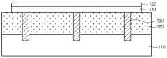
도 1은 본 발명의 제1 실시예에 따른 이미지센서의 단면도이다.1 is a cross-sectional view of an image sensor according to a first embodiment of the present invention.
본 발명의 제1 실시예에 따른 이미지센서는 기판(110)상에 형성된 씨모스 회로(circuitry)(미도시); 상기 기판(110)상에 형성된 하부배선(140); 상기 하부배선(140) 상에 형성된 카본나노튜브(150); 상기 카본나노튜브(150)에 형성된 전도성 고분자(160); 및 상기 카본나노튜브(150) 상에 형성된 투명전극(170);을 포함할 수 있다.An image sensor according to a first embodiment of the present invention includes a CMOS circuit (circuitry) (not shown) formed on the
본 발명의 제1 실시예에서 상기 카본나노튜브(150)에서 전자(electron)를 전달하는 과정은 다음과 같다. 즉, 외부 빛에 의해 상기 전도성 고분자(160)에서 전자(electron)와 홀(hole)이 발생하고, 상기 전자(electron)는 쉽고 빠르게 카본나노튜브(150)를 통해 하부배선(140)으로 전달된다.In the first embodiment of the present invention, the process of transferring electrons from the
본 발명의 제1 실시예에서 상기 카본나노튜브(150)는 구조에 따라 금속성(metallic)과 반도체성(semiconductic)을 가질 수 있다.In the first embodiment of the present invention, the
또한, 본 발명의 제1 실시예에서 상기 카본나노튜브(150)는 단일벽(single-wall)형태 또는 다중벽(multy-wall)형태 일수 있다. 단일벽 형태란 카본나노튜브(150)가 하나의 원기둥과 같은 형태를 의미하며, 다중벽형태란 카본나노튜브(150)가 여러 겹으로 이루어질 수 있음을 의미한다.In addition, in the first embodiment of the present invention, the
또한, 본 발명의 제1 실시예에서 상기 하부배선(140)은 기판(110)의 층간절연층(120)에 형성된 배선(130)과 전기적으로 연결될 수 있다.In addition, in the first embodiment of the present invention, the
또한, 본 발명의 제1 실시예는 픽셀간의 크로스토크를 방지하기 위한 절연 체(180)을 더 포함할 수 있으며, 상기 절연체(180)는 제1 절연체(182), 메탈(184), 제2 절연체(186)를 포함할 수 있다.In addition, the first embodiment of the present invention may further include an
또한, 본 발명의 제1 실시예에서는 상기 투명전극(170) 상에 형성된 컬러필터(190)와 마이크로렌즈(200)를 더 포함할 수 있다.In addition, the first embodiment of the present invention may further include a
이러한 본 발명의 제1 실시예에 따른 이미지센서에 의하면 트랜지스터 회로(circuitry)와 포토다이오드의 수직형 집적을 제공할 수 있다.According to the image sensor according to the first embodiment of the present invention, it is possible to provide vertical integration of a transistor circuit and a photodiode.
또한, 본 발명의 제1 실시예에 의하면 카본나노튜브를 이용해 포토다이오드를 형성함으로써 양자효율(quantum efficiency)을 높일 수 있는 효과가 있다.In addition, according to the first embodiment of the present invention, by forming a photodiode using carbon nanotubes, there is an effect of increasing quantum efficiency.
또한, 본 발명의 제1 실시예에 의하면 트랜지스터 회로(circuitry)와 포토다이오드의 수직형 집적에 의해 필팩터(fill factor)를 100%에 근접시킬 수 있다.In addition, according to the first embodiment of the present invention, the fill factor can be approached to 100% by vertical integration of the transistor circuit and the photodiode.
또한, 본 발명의 제1 실시예에 의하면 종래기술보다 수직형 집적에 의해 같은 픽셀 사이즈에서 높은 센서티버티(sensitivity)를 제공할 수 있다.Further, according to the first embodiment of the present invention, higher sensitivity can be provided at the same pixel size by vertical integration than in the prior art.
또한, 본 발명의 제1 실시예에 의하면 종래기술보다 같은 레졀류션(Resolution)을 위해 공정비용을 감축할 수 있다.In addition, according to the first embodiment of the present invention can reduce the process cost for the same resolution (Resolution) than the prior art.
또한, 본 발명의 제1 실시예에 의하면 각 단위 픽셀은 센서티버티(sensitivity)의 감소 없이 더욱 복잡한 회로(circuitry)를 구현할 수 있다.In addition, according to the first embodiment of the present invention, each unit pixel may implement a more complicated circuit without reducing the sensitivity.
또한, 본 발명의 실시예에 의해 집적될 수 있는 추가적인 온칩 회로(on-chip circuitry)는 이미지센서의 퍼포먼스(performance)를 증가시키고, 나아가 소자의 소형화 및 제조비용을 절감을 획득할 수 있다.In addition, the additional on-chip circuitry that can be integrated by the embodiment of the present invention can increase the performance of the image sensor, and further obtain the miniaturization and manufacturing cost of the device.
또한, 본 발명의 제1 실시예에 의하면 수직형의 포토다이오드를 채용하면서 포토다이오드 내에 디펙트를 방지할 수 있다.Further, according to the first embodiment of the present invention, it is possible to prevent defects in the photodiode while adopting a vertical photodiode.
이하, 도 2a 내지 도 2f를 참조하여 본 발명의 제1 실시예에 따른 이미지센서 제조방법을 설명한다.Hereinafter, a method of manufacturing an image sensor according to a first embodiment of the present invention will be described with reference to FIGS. 2A to 2F.
우선, 도 2a와 같이 씨모스 회로(circuitry)(미도시)를 기판(110)상에 형성한다. 상기 기판(110)에는 층간절연층(120)이 형성되고, 배선(130)이 형성될 수 있다.First, a CMOS circuit (not shown) is formed on the
이후, 상기 기판(110)상에 상기 배선(130)과 전기적으로 연결되는 하부배선(140)을 형성한다.Thereafter, a
다음으로, 상기 하부배선(140) 상에 촉매제(152)를 형성한다. 예를 들어, 촉매제(152)로 강자성 특성을 갖는 Co, Fe, Ni 등을 이용할 수 있다.Next, the
본 발명의 제1 실시예에서 상기 카본나노튜브(150)는 강자성 특성을 갖는 Co, Fe, Ni 등 상에서 증착되는 특성이 있기 때문에, 촉매제(152)을 이용하여 선택적으로 증착할 수 있다.In the first embodiment of the present invention, since the
다음으로, 도 2b와 같이 포토공정에 의해 촉매제(152)와 하부배선(140)을 선택적으로 패터닝한다.Next, as shown in FIG. 2B, the
다음으로, 도 2c와 같이 잔존하는 촉매제(152) 상에 카본나노튜브(150)를 선택적으로 증착한다. 예를 들어, 촉매제(152) 상에 카본나노튜브(150)를 10Å 내지 100,000 Å로 수직 증착할 수 있다.Next,
또한, 본 발명의 제1 실시예에서는 플라즈마처리(plasma treatment)로 촉매제를 활성화시켜 카본나노튜브(150)의 선택적으로 증착을 촉진할 수 있다.In addition, in the first embodiment of the present invention, the deposition of the
다음으로, 도 2d와 같이 상기 카본나노튜브(150)를 전도성 고분자(160)로 코팅할 수 있다. 예를 들어, 상기 전도성 고분자(160)는 공액 고분자(conjugated polymer)를 이용할 수 있다.Next, as shown in FIG. 2d, the
예를 들어, 상기 전도성 고분자(160)을 형성하는 방법으로는 폴리싸이오펜(polythiophene) 혹은 그의 유도체인 폴리(3,4-에틸렌디옥시싸이오펜), 폴리 아닐린(polyaniline), 폴리피롤(polypyrrole) 및 그의 유도체로 형성된 고분자, 혹은 공액(conjugated)구조를 갖는 고분자 등을 이용하여 열 경화 및 UV 경화에 의해 코팅하는 방법과 상기 전도성 고분자의 단량체를 인시튜(in-situ) 방법에 의해 코팅할 수 있다.For example, the method of forming the
다음으로, 상기 카본나노튜브(150) 상에 투명전극(transparent conducting electrode: TCE)(170)을 증착한다.Next, a transparent conducting electrode (TCE) 170 is deposited on the
다음으로, 도 2e와 같이 포토공정(photolithography) 및 식각(etch) 공정을 통해 패터닝을 완료하여 카본나노튜브(150)를 포함한 포토다이오드를 완성할 수 있다.Next, as shown in FIG. 2E, the patterning may be completed through a photolithography and an etching process to complete a photodiode including the
그 다음으로, 도 2f와 같이 픽셀간의 크로스토크를 방지하기 위한 절연체(180)을 더 형성할 수 있다. 상기 절연체(180)는 제1 절연체(182), 메탈(184), 제2 절연체(186)를 포함할 수 있다.Next, as shown in FIG. 2F, an
예를 들어, 상기 절연체(180)는 산화막인 제1 절연체(182), 메탈(184), 산화막인 제2 절연체(186)로 형성될 수 있다.For example, the
다음으로, 상기 투명전극(170) 상에 컬러필터(190)를 형성할 수 있다.Next, the
예를 들어, 상기 컬러필터(190)는 상기 투명전극(170) 상에 가염성레지스트를 사용하여 도포한 후, 노광 및 현상 공정을 진행하여 각각의 파장대별로 빛을 필터링하는 R, G, B의 컬러필터(190)를 형성할 수 있다. 이때, 상기 투명전극(170) 상에 절연층(미도시)을 추가로 형성하고, 상기 절연층 상에 컬러필터를 형성할 수도 있다.For example, the
이후, 상기 컬러필터(190)상에 초점거리 조절 및 렌즈층을 형성하기 위한 평탄도확보 등을 위하여 평탄화층(PL:planarization layer)(미도시)을 더 형성할 수 있다.Subsequently, a planarization layer (PL) (not shown) may be further formed on the
다음으로, 상기 컬러필터(190) 상에 마이크로렌즈(200)를 형성한다.Next, the
예를 들어, 상기 컬러필터(190) 상에 마이크로렌즈용 감광막(미도시)를 도포하고, 마이크로렌즈용 마스크(미도시)를 이용하여 노광 및 현상 공정으로 상기 감광막을 선택적으로 패터닝하여 감광막 패턴(미도시)을 형성한다.For example, a microlens photosensitive film (not shown) is coated on the
이후, 상기 감광막패턴이 형성된 기판(110)을 핫 플레이트(hot plate)(미도시) 상부에 올려놓은 상태에서 150℃ 이상의 열처리로 상부에 존재하는 감광막패턴을 리플로우하여 반구형의 마이크로렌즈(200)를 형성할 수 있다.Subsequently, in a state where the
다음으로, 상기 마이크로렌즈(200)상에 보호막(미도시)을 더 형성할 수 있다. 예를 들어, 상기 마이크로렌즈(200)상에 투명산화막으로된 보호막을 형성할 수 있으나, 이에 한정되는 것은 아니다.Next, a protective film (not shown) may be further formed on the
본 발명의 제1 실시예에 따른 이미지센의 제조방법에 의하면 트랜지스터 회로(circuitry)와 포토다이오드의 수직형 집적을 제공할 수 있고, 또한, 본 발명의 제1 실시예에 의하면 카본나노튜브를 이용해 포토다이오드를 형성함으로써 양자효율(quantum efficiency)을 높일 수 있는 효과가 있다.According to the manufacturing method of the image sensor according to the first embodiment of the present invention, it is possible to provide vertical integration of a transistor circuit and a photodiode. Further, according to the first embodiment of the present invention, a carbon nanotube is used. By forming a photodiode, there is an effect of increasing quantum efficiency.
(제2 실시예)(2nd Example)
도 3는 본 발명의 제2 실시예에 따른 이미지센서의 단면도이다.3 is a cross-sectional view of an image sensor according to a second exemplary embodiment of the present invention.
본 발명의 제2 실시예에 따른 이미지센서는 상기 제1 실시예에 따른 이미지센서의 기본적인 특징을 채용할 수 있다.The image sensor according to the second embodiment of the present invention may employ the basic features of the image sensor according to the first embodiment.
다만, 본 발명의 제2 실시예에 따른 이미지센서는 상기 제1 실시예와 달리 상기 하부배선(140) 상에 형성된 제1 도전형 전도층(210)을 더 포함하고, 상기 카본나노튜브(150a)는 제2 도전형으로 도전되어 상기 제1 도전형 전도층(210) 상에 형성되는 것을 특징으로 한다.However, unlike the first embodiment, the image sensor according to the second embodiment of the present invention further includes a first conductive type
예를 들어, 상기 제1 도전형 전도층(210)은 N 도핑된 비정질 실리콘(n-doped amorphous silicon)을 이용하여 형성될 수 있으나, 이에 한정되는 것은 아니다. 즉, 상기 제1 도전형 전도층(210)은 비정질 실리콘에 게르마늄, 탄소, 질소 또는 산소 등을 첨가하여 a-Si:H, a-SiGe:H, a-SiC, a-SiN:H a-SiO:H 등으로 형성될 수도 있다.For example, the first conductivity type
상기 제1 도전형 전도층(210)은 화학기상증착(CVD) 특히, PECVD 등에 의해 형성될 수 있다. 예를 들어, 상기 제1 도전형 전도층(210)은 실란가스(SiH4)에 PH3, P2H5 등을 혼합하여 PECVD에 의해 비정질 실리콘으로 형성될 수 있다.The first conductivity type
이때, 제2 실시예에서 상기 카본나노튜브(150a)는 P형으로 도전될 수 있으나 이에 한정되는 것은 아니다.At this time, in the second embodiment, the
본 발명의 제2 실시예에 따른 이미지센서 및 그 제조방법에 의하면 트랜지스터 회로(circuitry)와 포토다이오드의 수직형 집적을 제공할 수 있고, 또한, 본 발명의 제2 실시예에 의하면 카본나노튜브를 이용해 포토다이오드를 형성함으로써 양자효율(quantum efficiency)을 높일 수 있는 효과가 있다.According to an image sensor and a method of manufacturing the same according to the second embodiment of the present invention, it is possible to provide vertical integration of a transistor circuit and a photodiode, and according to a second embodiment of the present invention, Forming a photodiode using the photodiode has the effect of increasing quantum efficiency.
(제3 실시예)(Third Embodiment)
도 4는 본 발명의 제3 실시예에 따른 이미지센서의 단면도이다.4 is a cross-sectional view of an image sensor according to a third exemplary embodiment of the present invention.
본 발명의 제3 실시예에 따른 이미지센서는 상기 제1 실시예 및 상기 제2 실시예에 따른 이미지센서의 기본적인 특징을 채용할 수 있다.The image sensor according to the third embodiment of the present invention may employ the basic features of the image sensor according to the first and second embodiments.
다만, 본 발명의 제3 실시예에 따른 이미지센서는 상기 제2 실시예에 따른 이미지센서와는 달리 상기 제1 도전형 전도층(210) 상에 형성된 진성층(intrinsic layer)(220)을 더 포함하고, 카본나노튜브(150a)는 제2 도전형으로 도전되어 상기 진성층(220) 상에 형성될 수 있다.However, unlike the image sensor according to the second embodiment, the image sensor according to the third embodiment of the present invention further includes an
예를 들어, 상기 진성층(220)은 비정질 실리콘(amorphous silicon)을 이용하여 형성될 수 있다. 상기 진성층(220)은 화학기상증착(CVD) 특히, PECVD 등에 의해 형성될 수 있다. 예를 들어, 상기 진성층(220)은 실란가스(SiH4) 등을 이용하여 PECVD에 의해 비정질 실리콘으로 형성될 수 있다.For example, the
본 발명의 제3 실시예에 따른 이미지센서 및 그 제조방법에 의하면 트랜지스터 회로(circuitry)와 포토다이오드의 수직형 집적을 제공할 수 있고, 또한, 본 발 명의 제3 실시예에 의하면 카본나노튜브를 이용해 포토다이오드를 형성함으로써 양자효율(quantum efficiency)을 높일 수 있는 효과가 있다.According to an image sensor and a method of manufacturing the same according to the third embodiment of the present invention, it is possible to provide vertical integration of a transistor circuit and a photodiode, and furthermore, according to the third embodiment of the present invention, Forming a photodiode using the photodiode has the effect of increasing quantum efficiency.
(제4 실시예)(Example 4)
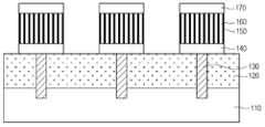
도 5는 본 발명의 제4 실시예에 따른 이미지센서의 단면도이다.5 is a cross-sectional view of an image sensor according to a fourth exemplary embodiment of the present invention.
본 발명의 제4 실시예에 따른 이미지센서는 상기 제1 실시예, 상기 제2 실시예 및 상기 제3 실시예에 따른 이미지센서의 기본적인 특징을 채용할 수 있다.The image sensor according to the fourth embodiment of the present invention may employ the basic features of the image sensor according to the first embodiment, the second embodiment, and the third embodiment.
다만, 본 발명의 제4 실시예에 따른 이미지센서는 상기 제2 실시예, 상기 제3 실시예와는 달리 카본나노튜브(150b)는 제1 도전형으로 도전되어 형성되고, 상기 제1 도전형 카본나노튜브(150b) 상에 형성된 진성층(220) 및 상기 진성층(220) 상에 형성된 제2 도전형 전도층(230)을 포함할 수 있다.However, in the image sensor according to the fourth embodiment of the present invention, unlike the second embodiment and the third embodiment, the
예를 들어, 상기 카본나노튜브(150b)는 N형으로 도전될 수 있으나, 이에 한정되는 것은 아니다.For example, the
또한, 상기 제2 도전형 전도층(230)은 상기 진성층(220)의 형성과 연속공정으로 형성될 수 있다. 상기 제2 도전형 전도층(230)은 P 도핑된 비정질 실리콘(p-doped amorphous silicon)을 이용하여 형성될 수 있으나, 이에 한정되는 것은 아니다.In addition, the second conductivity type
상기 제2 도전형 전도층(230)은 화학기상증착(CVD) 특히, PECVD 등에 의해 형성될 수 있다. 예를 들어, 상기 제2 도전형 전도층(230)은 실란가스(SiH4)에 보론 등을 혼합하여 PECVD에 의해 비정질 실리콘으로 형성될 수 있다.The second conductivity type
본 발명의 제4 실시예에 따른 이미지센서 및 그 제조방법에 의하면 트랜지스터 회로(circuitry)와 포토다이오드의 수직형 집적을 제공할 수 있고, 또한, 본 발명의 제4 실시예에 의하면 카본나노튜브를 이용해 포토다이오드를 형성함으로써 양자효율(quantum efficiency)을 높일 수 있는 효과가 있다.According to the image sensor and the manufacturing method thereof according to the fourth embodiment of the present invention, it is possible to provide vertical integration of a transistor circuit and a photodiode, and furthermore, according to the fourth embodiment of the present invention, Forming a photodiode using the photodiode has the effect of increasing quantum efficiency.
(제5 실시예)(Example 5)
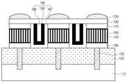
도 6은 본 발명의 제5 실시예에 따른 이미지센서의 단면도이다.6 is a cross-sectional view of an image sensor according to a fifth exemplary embodiment of the present invention.
본 발명의 제5 실시예에 따른 이미지센서는 상기 제1 실시예에 따른 이미지센서의 기본적인 특징을 채용할 수 있다.The image sensor according to the fifth embodiment of the present invention may employ the basic features of the image sensor according to the first embodiment.
다만, 본 발명의 제5 실시예에 따른 이미지센서는 상기 제1 실시예와 달리 상기 전도성 고분자는 컬러폴리머로 형성될 수 있다.However, in the image sensor according to the fifth embodiment of the present invention, the conductive polymer may be formed of a color polymer unlike the first embodiment.
이에 따라, 상기 제5 실시예에서는 별도의 컬러필터가 채용되지 않을 수 있다.Accordingly, a separate color filter may not be employed in the fifth embodiment.
즉, 본 발명의 제5 실시예에서의 전도성 고분자는 제1 색의 전도성 고분자(162), 제2 색의 전도성 고분자(164), 제3 색의 전도성 고분자(166)를 포함할 수 있다.That is, the conductive polymer in the fifth embodiment of the present invention may include the
예를 들어, 제5 실시예에서의 전도성 고분자는 적색(R)의 전도성 고분자(162), 녹색(G)의 전도성 고분자(164), 파란색(B)의 전도성 고분자(166)를 포함할 수 있다For example, the conductive polymer in the fifth embodiment may include a
본 발명의 제5 실시예에 따른 이미지센서 및 그 제조방법에 의하면 트랜지스터 회로(circuitry)와 포토다이오드의 수직형 집적을 제공할 수 있고, 또한, 본 발 명의 제5 실시예에 의하면 카본나노튜브를 이용해 포토다이오드를 형성함으로써 양자효율(quantum efficiency)을 높일 수 있고, 또한 컬러폴리머을 이용한 전도성 고분자를 채용함으로써 별도의 컬러필터 없이 색깔을 필터링할 수 있는 효과가 있다.According to an image sensor and a method of manufacturing the same according to a fifth embodiment of the present invention, it is possible to provide vertical integration of a transistor circuit and a photodiode, and according to a fifth embodiment of the present invention, By forming a photodiode by using a quantum efficiency (quantum efficiency) can be increased, and by adopting a conductive polymer using a color polymer there is an effect that can filter the color without a separate color filter.
본 발명은 전술한 실시예 및 도면에 의해 한정되는 것이 아니고, 하기 된 청구항의 권리범위에 속하는 범위 안에서 다양한 다른 실시예가 가능하다.The present invention is not limited by the above-described embodiments and drawings, and various other embodiments are possible within the scope of the claims.
본 발명의 실시예에 따른 이미지센서 및 그 제조방법에 의하면 트랜지스터 회로(circuitry)와 포토다이오드의 수직형 집적을 제공할 수 있다.According to an image sensor and a method of manufacturing the same according to an embodiment of the present invention, it is possible to provide a vertical integration of a transistor circuit and a photodiode.
또한, 본 발명의 실시예에 의하면 카본나노튜브를 이용해 포토다이오드를 형성함으로써 양자효율(quantum efficiency)을 높일 수 있는 효과가 있다.In addition, according to an embodiment of the present invention by forming a photodiode using carbon nanotubes there is an effect that can increase the quantum efficiency (quantum efficiency).
또한, 본 발명의 실시예에 의하면 트랜지스터 회로(circuitry)와 포토다이오드의 수직형 집적에 의해 필팩터(fill factor)를 100%에 근접시킬 수 있다.In addition, according to the exemplary embodiment of the present invention, the fill factor may be approached to 100% by vertical integration of the transistor circuit and the photodiode.
또한, 본 발명의 실시예에 의하면 종래기술보다 수직형 집적에 의해 같은 픽셀 사이즈에서 높은 센서티버티(sensitivity)를 제공할 수 있다.In addition, according to an embodiment of the present invention, it is possible to provide higher sensitivity at the same pixel size by vertical integration than in the prior art.
또한, 본 발명의 실시예에 의하면 종래기술보다 같은 레졀류션(Resolution)을 위해 공정비용을 감축할 수 있다.In addition, according to an embodiment of the present invention it is possible to reduce the process cost for the same resolution (Resolution) than the prior art.
또한, 본 발명의 실시예에 의하면 각 단위 픽셀은 센서티버티(sensitivity)의 감소 없이 더욱 복잡한 회로(circuitry)를 구현할 수 있다.In addition, according to an exemplary embodiment of the present invention, each unit pixel may implement a more complicated circuit without reducing the sensitivity.
또한, 본 발명의 실시예에 의해 집적될 수 있는 추가적인 온칩 회로(on-chip circuitry)는 이미지센서의 퍼포먼스(performance)를 증가시키고, 나아가 소자의 소형화 및 제조비용을 절감을 획득할 수 있다.In addition, the additional on-chip circuitry that can be integrated by the embodiment of the present invention can increase the performance of the image sensor, and further obtain the miniaturization and manufacturing cost of the device.
또한, 본 발명의 실시예에 의하면 수직형의 포토다이오드를 채용하면서 포토다이오드 내에 디펙트를 방지할 수 있다.Further, according to the embodiment of the present invention, it is possible to prevent defects in the photodiode while employing a vertical photodiode.
Claims (11)
Translated fromKoreanPriority Applications (6)
| Application Number | Priority Date | Filing Date | Title |
|---|---|---|---|
| KR1020070047589AKR100901236B1 (en) | 2007-05-16 | 2007-05-16 | Image sensor and manufacturing method |
| US12/119,838US7732805B2 (en) | 2007-05-16 | 2008-05-13 | Image sensor and method for manufacturing the same |
| JP2008125701AJP4982426B2 (en) | 2007-05-16 | 2008-05-13 | Image sensor and manufacturing method thereof |
| DE102008023461ADE102008023461A1 (en) | 2007-05-16 | 2008-05-14 | Image sensor and method for its production |
| TW097118264ATW200847412A (en) | 2007-05-16 | 2008-05-16 | Image sensor and method for manufacturing the same |
| CN2008100992961ACN101308862B (en) | 2007-05-16 | 2008-05-16 | Image sensor and manufacturing method thereof |
Applications Claiming Priority (1)
| Application Number | Priority Date | Filing Date | Title |
|---|---|---|---|
| KR1020070047589AKR100901236B1 (en) | 2007-05-16 | 2007-05-16 | Image sensor and manufacturing method |
Publications (2)
| Publication Number | Publication Date |
|---|---|
| KR20080101189A KR20080101189A (en) | 2008-11-21 |
| KR100901236B1true KR100901236B1 (en) | 2009-06-08 |
Family
ID=39917571
Family Applications (1)
| Application Number | Title | Priority Date | Filing Date |
|---|---|---|---|
| KR1020070047589AExpired - Fee RelatedKR100901236B1 (en) | 2007-05-16 | 2007-05-16 | Image sensor and manufacturing method |
Country Status (6)
| Country | Link |
|---|---|
| US (1) | US7732805B2 (en) |
| JP (1) | JP4982426B2 (en) |
| KR (1) | KR100901236B1 (en) |
| CN (1) | CN101308862B (en) |
| DE (1) | DE102008023461A1 (en) |
| TW (1) | TW200847412A (en) |
Families Citing this family (32)
| Publication number | Priority date | Publication date | Assignee | Title |
|---|---|---|---|---|
| US8269985B2 (en) | 2009-05-26 | 2012-09-18 | Zena Technologies, Inc. | Determination of optimal diameters for nanowires |
| US8889455B2 (en) | 2009-12-08 | 2014-11-18 | Zena Technologies, Inc. | Manufacturing nanowire photo-detector grown on a back-side illuminated image sensor |
| US9082673B2 (en) | 2009-10-05 | 2015-07-14 | Zena Technologies, Inc. | Passivated upstanding nanostructures and methods of making the same |
| US8229255B2 (en) | 2008-09-04 | 2012-07-24 | Zena Technologies, Inc. | Optical waveguides in image sensors |
| US8384007B2 (en)* | 2009-10-07 | 2013-02-26 | Zena Technologies, Inc. | Nano wire based passive pixel image sensor |
| US9406709B2 (en) | 2010-06-22 | 2016-08-02 | President And Fellows Of Harvard College | Methods for fabricating and using nanowires |
| US8791470B2 (en) | 2009-10-05 | 2014-07-29 | Zena Technologies, Inc. | Nano structured LEDs |
| US9299866B2 (en) | 2010-12-30 | 2016-03-29 | Zena Technologies, Inc. | Nanowire array based solar energy harvesting device |
| US8519379B2 (en) | 2009-12-08 | 2013-08-27 | Zena Technologies, Inc. | Nanowire structured photodiode with a surrounding epitaxially grown P or N layer |
| US9343490B2 (en) | 2013-08-09 | 2016-05-17 | Zena Technologies, Inc. | Nanowire structured color filter arrays and fabrication method of the same |
| US8507840B2 (en) | 2010-12-21 | 2013-08-13 | Zena Technologies, Inc. | Vertically structured passive pixel arrays and methods for fabricating the same |
| US9000353B2 (en) | 2010-06-22 | 2015-04-07 | President And Fellows Of Harvard College | Light absorption and filtering properties of vertically oriented semiconductor nano wires |
| US8835831B2 (en) | 2010-06-22 | 2014-09-16 | Zena Technologies, Inc. | Polarized light detecting device and fabrication methods of the same |
| US8748799B2 (en) | 2010-12-14 | 2014-06-10 | Zena Technologies, Inc. | Full color single pixel including doublet or quadruplet si nanowires for image sensors |
| US8546742B2 (en) | 2009-06-04 | 2013-10-01 | Zena Technologies, Inc. | Array of nanowires in a single cavity with anti-reflective coating on substrate |
| US9515218B2 (en) | 2008-09-04 | 2016-12-06 | Zena Technologies, Inc. | Vertical pillar structured photovoltaic devices with mirrors and optical claddings |
| US8735797B2 (en) | 2009-12-08 | 2014-05-27 | Zena Technologies, Inc. | Nanowire photo-detector grown on a back-side illuminated image sensor |
| US8299472B2 (en)* | 2009-12-08 | 2012-10-30 | Young-June Yu | Active pixel sensor with nanowire structured photodetectors |
| US8274039B2 (en) | 2008-11-13 | 2012-09-25 | Zena Technologies, Inc. | Vertical waveguides with various functionality on integrated circuits |
| US8866065B2 (en) | 2010-12-13 | 2014-10-21 | Zena Technologies, Inc. | Nanowire arrays comprising fluorescent nanowires |
| US20100148221A1 (en)* | 2008-11-13 | 2010-06-17 | Zena Technologies, Inc. | Vertical photogate (vpg) pixel structure with nanowires |
| US9478685B2 (en) | 2014-06-23 | 2016-10-25 | Zena Technologies, Inc. | Vertical pillar structured infrared detector and fabrication method for the same |
| US8890271B2 (en) | 2010-06-30 | 2014-11-18 | Zena Technologies, Inc. | Silicon nitride light pipes for image sensors |
| JP2014022448A (en) | 2012-07-13 | 2014-02-03 | Toshiba Corp | Solid-state imaging device |
| KR102338334B1 (en) | 2014-07-17 | 2021-12-09 | 삼성전자주식회사 | Organic photoelectronic device and image sensor and electronic device |
| KR102294724B1 (en)* | 2014-12-02 | 2021-08-31 | 삼성디스플레이 주식회사 | Organic light emitting transistor and display apparatus having the same |
| KR102441585B1 (en)* | 2015-02-12 | 2022-09-07 | 삼성전자주식회사 | Photodetecting element and manufacturing method thereof, image sensor and manufacturing method thereof |
| JP6161018B2 (en)* | 2015-07-08 | 2017-07-12 | パナソニックIpマネジメント株式会社 | Imaging device |
| CN106206634A (en)* | 2016-07-27 | 2016-12-07 | 上海集成电路研发中心有限公司 | A kind of image sensor architecture and preparation method thereof |
| KR101938879B1 (en) | 2017-10-27 | 2019-01-15 | 엘지디스플레이 주식회사 | Display Apparatus |
| CN113396125B (en)* | 2019-05-07 | 2025-07-04 | 松下知识产权经营株式会社 | Camera device |
| JP7595307B2 (en)* | 2019-10-31 | 2024-12-06 | パナソニックIpマネジメント株式会社 | Photoelectric conversion element, electronic device and light-emitting device |
Citations (2)
| Publication number | Priority date | Publication date | Assignee | Title |
|---|---|---|---|---|
| KR20040095502A (en)* | 2003-05-09 | 2004-11-15 | 한국원자력연구소 | A thermal neutron image device using carbon-nanotube |
| US6841411B1 (en)* | 2003-06-30 | 2005-01-11 | Agilent Technologies, Inc. | Method of utilizing a top conductive layer in isolating pixels of an image sensor array |
Family Cites Families (13)
| Publication number | Priority date | Publication date | Assignee | Title |
|---|---|---|---|---|
| JPS58103165A (en)* | 1981-12-15 | 1983-06-20 | Fuji Photo Film Co Ltd | Solid-state color image pickup device of tripple-layer four-story structure |
| US5300374A (en)* | 1992-08-31 | 1994-04-05 | Donnelly Corporation | Ion conducting polymers |
| JP2003050280A (en)* | 2001-08-03 | 2003-02-21 | Konica Corp | Radiographic image detector |
| WO2003049219A1 (en)* | 2001-11-30 | 2003-06-12 | The Trustees Of Boston College | Coated carbon nanotube array electrodes |
| JP2004085392A (en)* | 2002-08-27 | 2004-03-18 | Fujitsu Ltd | Field effect transistor chemical sensor using elemental carbon linear structure |
| US20050244811A1 (en)* | 2003-12-15 | 2005-11-03 | Nano-Proprietary, Inc. | Matrix array nanobiosensor |
| WO2005096403A2 (en)* | 2004-03-31 | 2005-10-13 | Matsushita Electric Industrial Co., Ltd. | Organic photoelectric conversion element utilizing an inorganic buffer layer placed between an electrode and the active material |
| JP2005294303A (en)* | 2004-03-31 | 2005-10-20 | Matsushita Electric Ind Co Ltd | Organic photoelectric conversion element and manufacturing method thereof |
| KR100624433B1 (en)* | 2004-08-13 | 2006-09-19 | 삼성전자주식회사 | P-type semiconductor carbon nanotubes and a method of manufacturing the same |
| US7535016B2 (en) | 2005-01-31 | 2009-05-19 | International Business Machines Corporation | Vertical carbon nanotube transistor integration |
| JP2007043150A (en)* | 2005-07-29 | 2007-02-15 | Interuniv Micro Electronica Centrum Vzw | Wavelength sensitive detector with elongated nanostructures |
| US20070148963A1 (en)* | 2005-12-27 | 2007-06-28 | The Hong Kong University Of Science And Technology | Semiconductor devices incorporating carbon nanotubes and composites thereof |
| US7679157B2 (en)* | 2006-08-21 | 2010-03-16 | Powerchip Semiconductor Corp. | Image sensor and fabrication method thereof |
- 2007
- 2007-05-16KRKR1020070047589Apatent/KR100901236B1/ennot_activeExpired - Fee Related
- 2008
- 2008-05-13JPJP2008125701Apatent/JP4982426B2/ennot_activeExpired - Fee Related
- 2008-05-13USUS12/119,838patent/US7732805B2/ennot_activeExpired - Fee Related
- 2008-05-14DEDE102008023461Apatent/DE102008023461A1/ennot_activeWithdrawn
- 2008-05-16TWTW097118264Apatent/TW200847412A/enunknown
- 2008-05-16CNCN2008100992961Apatent/CN101308862B/ennot_activeExpired - Fee Related
Patent Citations (2)
| Publication number | Priority date | Publication date | Assignee | Title |
|---|---|---|---|---|
| KR20040095502A (en)* | 2003-05-09 | 2004-11-15 | 한국원자력연구소 | A thermal neutron image device using carbon-nanotube |
| US6841411B1 (en)* | 2003-06-30 | 2005-01-11 | Agilent Technologies, Inc. | Method of utilizing a top conductive layer in isolating pixels of an image sensor array |
Non-Patent Citations (1)
| Title |
|---|
| Chemistry of Materials, Vol.16, No.23, pp.4819-4823(2004)* |
Also Published As
| Publication number | Publication date |
|---|---|
| CN101308862A (en) | 2008-11-19 |
| JP2008288585A (en) | 2008-11-27 |
| CN101308862B (en) | 2011-01-19 |
| TW200847412A (en) | 2008-12-01 |
| US20080283883A1 (en) | 2008-11-20 |
| DE102008023461A1 (en) | 2008-12-04 |
| KR20080101189A (en) | 2008-11-21 |
| JP4982426B2 (en) | 2012-07-25 |
| US7732805B2 (en) | 2010-06-08 |
Similar Documents
| Publication | Publication Date | Title |
|---|---|---|
| KR100901236B1 (en) | Image sensor and manufacturing method | |
| CN101325206B (en) | Image sensor and method for manufacturing thereof | |
| KR100851756B1 (en) | Image sensor and its manufacturing method | |
| US7935560B2 (en) | Imagers having electrically active optical elements | |
| US7671385B2 (en) | Image sensor and fabrication method thereof | |
| JP2015073070A (en) | Imaging apparatus having partition wall of photoelectric conversion layer | |
| US7812350B2 (en) | Image sensor and method for manufacturing the same | |
| CN101399278B (en) | Image sensor and method for manufacturing the same | |
| KR100843965B1 (en) | Image sensor and manufacturing method | |
| KR100881012B1 (en) | Image sensor and manufacturing method | |
| US20080230783A1 (en) | Image Sensor and Method for Manufacturing the Same | |
| KR100872990B1 (en) | Image sensor and its manufacturing method | |
| KR100866255B1 (en) | Image sensor and its manufacturing method | |
| KR100894390B1 (en) | Image sensor and its manufacturing method | |
| CN101266987A (en) | Image sensor and manufacturing method thereof | |
| KR20090046170A (en) | Image sensor and manufacturing method | |
| KR100906061B1 (en) | Image sensor and its manufacturing method | |
| CN101266988A (en) | Image sensor and manufacturing method thereof | |
| KR100904828B1 (en) | Image sensor and manufacturing method | |
| KR100881011B1 (en) | Image sensor and manufacturing method | |
| KR100915751B1 (en) | Image Sensor and Method for Manufacturing Thereof | |
| JP2021174930A (en) | Imaging device and imaging system | |
| KR20090070378A (en) | CMOS image sensor and its manufacturing method |
Legal Events
| Date | Code | Title | Description |
|---|---|---|---|
| A201 | Request for examination | ||
| PA0109 | Patent application | St.27 status event code:A-0-1-A10-A12-nap-PA0109 | |
| PA0201 | Request for examination | St.27 status event code:A-1-2-D10-D11-exm-PA0201 | |
| PN2301 | Change of applicant | St.27 status event code:A-3-3-R10-R13-asn-PN2301 St.27 status event code:A-3-3-R10-R11-asn-PN2301 | |
| D13-X000 | Search requested | St.27 status event code:A-1-2-D10-D13-srh-X000 | |
| D14-X000 | Search report completed | St.27 status event code:A-1-2-D10-D14-srh-X000 | |
| E902 | Notification of reason for refusal | ||
| PE0902 | Notice of grounds for rejection | St.27 status event code:A-1-2-D10-D21-exm-PE0902 | |
| AMND | Amendment | ||
| P11-X000 | Amendment of application requested | St.27 status event code:A-2-2-P10-P11-nap-X000 | |
| P13-X000 | Application amended | St.27 status event code:A-2-2-P10-P13-nap-X000 | |
| E601 | Decision to refuse application | ||
| PE0601 | Decision on rejection of patent | St.27 status event code:N-2-6-B10-B15-exm-PE0601 | |
| PG1501 | Laying open of application | St.27 status event code:A-1-1-Q10-Q12-nap-PG1501 | |
| J201 | Request for trial against refusal decision | ||
| PJ0201 | Trial against decision of rejection | St.27 status event code:A-3-3-V10-V11-apl-PJ0201 | |
| AMND | Amendment | ||
| E13-X000 | Pre-grant limitation requested | St.27 status event code:A-2-3-E10-E13-lim-X000 | |
| P11-X000 | Amendment of application requested | St.27 status event code:A-2-2-P10-P11-nap-X000 | |
| P13-X000 | Application amended | St.27 status event code:A-2-2-P10-P13-nap-X000 | |
| PB0901 | Examination by re-examination before a trial | St.27 status event code:A-6-3-E10-E12-rex-PB0901 | |
| E902 | Notification of reason for refusal | ||
| PE0902 | Notice of grounds for rejection | St.27 status event code:A-1-2-D10-D21-exm-PE0902 | |
| E13-X000 | Pre-grant limitation requested | St.27 status event code:A-2-3-E10-E13-lim-X000 | |
| P11-X000 | Amendment of application requested | St.27 status event code:A-2-2-P10-P11-nap-X000 | |
| P13-X000 | Application amended | St.27 status event code:A-2-2-P10-P13-nap-X000 | |
| R17-X000 | Change to representative recorded | St.27 status event code:A-3-3-R10-R17-oth-X000 | |
| B701 | Decision to grant | ||
| PB0701 | Decision of registration after re-examination before a trial | St.27 status event code:A-3-4-F10-F13-rex-PB0701 | |
| GRNT | Written decision to grant | ||
| PR0701 | Registration of establishment | St.27 status event code:A-2-4-F10-F11-exm-PR0701 | |
| PR1002 | Payment of registration fee | St.27 status event code:A-2-2-U10-U11-oth-PR1002 Fee payment year number:1 | |
| PG1601 | Publication of registration | St.27 status event code:A-4-4-Q10-Q13-nap-PG1601 | |
| FPAY | Annual fee payment | Payment date:20120417 Year of fee payment:4 | |
| PR1001 | Payment of annual fee | St.27 status event code:A-4-4-U10-U11-oth-PR1001 Fee payment year number:4 | |
| LAPS | Lapse due to unpaid annual fee | ||
| PC1903 | Unpaid annual fee | St.27 status event code:A-4-4-U10-U13-oth-PC1903 Not in force date:20130530 Payment event data comment text:Termination Category : DEFAULT_OF_REGISTRATION_FEE | |
| PC1903 | Unpaid annual fee | St.27 status event code:N-4-6-H10-H13-oth-PC1903 Ip right cessation event data comment text:Termination Category : DEFAULT_OF_REGISTRATION_FEE Not in force date:20130530 | |
| PN2301 | Change of applicant | St.27 status event code:A-5-5-R10-R13-asn-PN2301 St.27 status event code:A-5-5-R10-R11-asn-PN2301 | |
| R18-X000 | Changes to party contact information recorded | St.27 status event code:A-5-5-R10-R18-oth-X000 | |
| P22-X000 | Classification modified | St.27 status event code:A-4-4-P10-P22-nap-X000 |