KR100900136B1 - 1-transistor DRAM - Google Patents
1-transistor DRAMDownload PDFInfo
- Publication number
- KR100900136B1 KR100900136B1KR1020070104561AKR20070104561AKR100900136B1KR 100900136 B1KR100900136 B1KR 100900136B1KR 1020070104561 AKR1020070104561 AKR 1020070104561AKR 20070104561 AKR20070104561 AKR 20070104561AKR 100900136 B1KR100900136 B1KR 100900136B1
- Authority
- KR
- South Korea
- Prior art keywords
- active region
- region
- word lines
- contact plug
- metal wiring
- Prior art date
- Legal status (The legal status is an assumption and is not a legal conclusion. Google has not performed a legal analysis and makes no representation as to the accuracy of the status listed.)
- Expired - Fee Related
Links
Images


Classifications
- H—ELECTRICITY
- H10—SEMICONDUCTOR DEVICES; ELECTRIC SOLID-STATE DEVICES NOT OTHERWISE PROVIDED FOR
- H10B—ELECTRONIC MEMORY DEVICES
- H10B12/00—Dynamic random access memory [DRAM] devices
- H—ELECTRICITY
- H10—SEMICONDUCTOR DEVICES; ELECTRIC SOLID-STATE DEVICES NOT OTHERWISE PROVIDED FOR
- H10B—ELECTRONIC MEMORY DEVICES
- H10B12/00—Dynamic random access memory [DRAM] devices
- H10B12/30—DRAM devices comprising one-transistor - one-capacitor [1T-1C] memory cells
- H10B12/48—Data lines or contacts therefor
- H10B12/482—Bit lines
Landscapes
- Semiconductor Memories (AREA)
Abstract
Translated fromKoreanDescription
Translated fromKorean본 발명은 1-트랜지스터형 디램에 관한 것으로, 특히 1-트랜지스터형 디램 구조에서 두 개의 트랜지스터가 하나의 소스를 공유하고, 비트라인이 활성영역 상부를 지나가도록 배치하여 셀 사이즈를 감소시킬 수 있는 기술이다.The present invention relates to a 1-transistor type DRAM, and in particular, in a 1-transistor type DRAM structure, two transistors share a single source, and a bit line is arranged to pass over an active region to reduce cell size. to be.
반도체 메모리장치로서 대표적인 소자는 디램(DRAM)이다. 디램은 일반적으로 하나의 트랜지스터(transistor)와 하나의 캐패시터(capacitor)로 이루어진 구성이 하나의 단위 셀(unit cell)을 이루게 된다.A typical device for a semiconductor memory device is DRAM. In general, a DRAM is composed of one transistor and one capacitor to form one unit cell.
디지탈 데이터(digital data) 1(=high) 또는 0(=low)은 캐패시터에 저장되며, 상기 캐패시터에 저장되는 데이터의 레벨을 정상적으로 유지하기 위해서, 디램은 일정 시간간격을 갖고 데이터 재충전동작인 리프레쉬(refresh)를 수행하게 된다. 이와 같은 단위 셀을 갖는 디램은 디디알 시리즈(DDR(Double Data Rate SDRAM) series)로 불리우는 동기형 반도체 메모리 장치까지 그 개발이 이루어지고 있다.Digital data 1 (= high) or 0 (= low) is stored in the capacitor, and in order to maintain the level of data stored in the capacitor normally, the DRAM has a predetermined time interval and refreshes the data recharging operation. refresh). The DRAM having such a unit cell has been developed to a synchronous semiconductor memory device called a DDR series (DDR (Double Data Rate SDRAM) series).
그러나, 디램의 집적도(density)가 기가(Giga)급으로 갈수록 칩의 면적은 점점 더 크게 구현될 수 밖에 없을 것이다. 이는 칩의 크기가 소형화될수록 유리하게 되는 시스템(system)의 입장에서는 부담으로 작용할 것이다.However, as DRAM density increases to Giga level, the chip area will have to be increased. This will be a burden for the system, which is advantageous as the size of the chip becomes smaller.
특히, 단위 셀을 구성하는 캐패시터는 캐패시터의 정전용량을 증가시키기 위해 하부 전극의 높이를 2μm 이상으로 높게 형성하고, 유전율이 높은 물질을 사용하고 있다. 이에 따라, 캐패시터를 패터닝하는데 어려움이 있고, 누설전류 발생이 증가하게 된다.In particular, the capacitor constituting the unit cell forms a height of the lower electrode of 2 μm or more in order to increase the capacitance of the capacitor, and uses a high dielectric constant material. As a result, there is a difficulty in patterning the capacitor and the leakage current is increased.
또한, 종래의 단위 셀 구조에 의해서는 비트라인이 활성영역 상부가 아닌 소자분리막 상부를 지나가도록 배치되어 디램(DRAM) 소자가 6F2 이하의 구조를 갖는데 한계가 있다.In addition, the conventional unit cell structure has a limitation in that the DRAM device has a structure of 6F2 or less because the bit line is disposed to pass over the device isolation layer instead of the upper portion of the active region.
본 발명은 다음과 같은 목적이 있다.The present invention has the following object.
첫째, 1-트랜지스터형 디램을 구현하여 캐패시터 공정을 없앰으로써 공정을 단순화시키고, 칩의 높이를 감소시킬 수 있는데 그 목적이 있다.First, the 1-transistor DRAM can be implemented to simplify the process and reduce the chip height by eliminating the capacitor process.
둘째, 두 개의 트랜지스터가 하나의 소스를 공유하고, 비트라인이 활성영역 상부를 지나가도록 배치하여 셀 사이즈를 감소시킬 수 있는데 그 목적이 있다.Secondly, two transistors share one source, and the bit line can be arranged to pass over the active region, thereby reducing the cell size.
셋째, 트랜지스터의 드레인 상부에 섬(island)형 금속배선을 형성하고, 섬형 금속배선과 접속하는 콘택플러그를 형성하여 드레인과 비트라인을 연결함으로써 콘택플러그의 높이를 낮춰 공정을 용이하게 하고, 드레인의 표면 데미지를 방지할 수 있는데 그 목적이 있다.Third, an island-type metal wiring is formed on the drain of the transistor, and a contact plug for connecting the island-type metal wiring is formed to connect the drain and the bit line to lower the height of the contact plug to facilitate the process. The purpose is to prevent surface damage.
본 발명에 따른 1-트랜지스터형 디램은 활성영역과 소자분리막을 가로지르는 제 1 및 제 2 워드라인; 제 1 및 제 2 워드라인 사이의 활성영역 내에 형성된 공통 소스 영역; 제 1 및 제 2 워드라인 외측부의 활성영역 내에 형성된 드레인 영역; 공통 소스 영역 및 드레인 영역과 각각 접속된 제 1 및 제 2 금속배선; 및 제 2 금속배선과 접속된 비트라인을 포함하는 것을 특징으로 한다.The 1-transistor DRAM according to the present invention includes first and second word lines across the active region and the device isolation layer; A common source region formed in an active region between the first and second word lines; A drain region formed in an active region outside the first and second word lines; First and second metal interconnections respectively connected to the common source region and the drain region; And a bit line connected to the second metal wiring.
본 발명은 다음과 같은 효과를 제공한다.The present invention provides the following effects.
첫째, 1-트랜지스터형 디램을 구현하여 캐패시터 공정을 없앰으로써 공정을 단순화시키고, 칩의 높이를 감소시킬 수 있는 효과를 제공한다.First, the 1-transistor DRAM can be implemented to simplify the process and reduce the chip height by eliminating the capacitor process.
둘째, 두 개의 트랜지스터가 하나의 소스를 공유하고, 비트라인이 활성영역 상부를 지나가도록 배치하여 셀 사이즈를 감소시킬 수 있는 효과를 제공한다.Second, the two transistors share a single source, and the bit line is arranged to pass over the active region, thereby reducing the cell size.
셋째, 트랜지스터의 드레인 상부에 섬(island)형 금속배선을 형성하고, 섬형 금속배선과 접속하는 콘택플러그를 형성하여 드레인과 비트라인을 연결함으로써 콘택플러그의 높이를 낮춰 공정을 용이하게 하고, 드레인의 표면 데미지를 방지할 수 있는 효과를 제공한다.Third, an island-type metal wiring is formed on the drain of the transistor, and a contact plug for connecting the island-type metal wiring is formed to connect the drain and the bit line to lower the height of the contact plug to facilitate the process. Provides the effect of preventing surface damage.
아울러 본 발명의 바람직한 실시예는 예시의 목적을 위한 것으로, 당업자라면 첨부된 특허청구범위의 기술적 사상과 범위를 통해 다양한 수정, 변경, 대체 및 부가가 가능할 것이며, 이러한 수정 변경 등은 이하의 특허청구범위에 속하는 것으로 보아야 할 것이다.In addition, a preferred embodiment of the present invention is for the purpose of illustration, those skilled in the art will be able to various modifications, changes, substitutions and additions through the spirit and scope of the appended claims, such modifications and changes are the following claims It should be seen as belonging to a range.
이하, 첨부한 도면을 참조하여 본 발명의 실시예에 대해 상세히 설명하고자 한다.Hereinafter, with reference to the accompanying drawings will be described in detail an embodiment of the present invention.
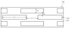
도 1a 내지 도 1f는 본 발명의 제 1 실시예에 따른 1-트랜지스터형 디램의 레이아웃을 도시한 도면이다.1A to 1F illustrate the layout of a one-transistor DRAM according to a first embodiment of the present invention.
먼저, 도 1a에 도시된 바와 같이, 반도체 기판(100)에 활성영역(102)을 정의하는 소자분리막(104)을 형성한다.First, as shown in FIG. 1A, an
여기서, 활성영역(102)은 I자 형태, T자 형태 및 Z자 형태 중 선택된 어느 하나로 형성하는 것이 바람직하다. 그리고, 활성영역(102)의 길이(a) 방향으로 중 심부의 폭과 가장자리부의 폭을 동일하거나 다르게 하는 형태로 형성할 수도 있다.Herein, the
그리고, 활성영역(102)의 장축방향 길이(a)는 후속 공정에서 형성될 비트라인과 평행한 방향으로 단축방향 길이(b) 보다 크게 형성하고, 활성영역(102)의 단축방향 길이(b)는 후속 공정에서 형성될 워드라인과 평행한 방향으로 형성하는 것이 바람직하다.In addition, the major axis length a of the
또한, 활성영역(102)의 장축방향 길이(a) 방향으로 이웃한 활성영역(102) 사이에 있는 영역의 길이(c)와 활성영역(102)의 단축방향 길이(b) 방향으로 이웃한 활성영역(102) 사이에 있는 영역의 길이(d)는 서로 다르게 형성하며, 길이(c)가 길이(d) 보다 크게 형성하는 것이 바람직하다.In addition, the length (c) of the area between the
그리고, 활성영역(102)의 장축방향 길이(a)와 이웃한 활성영역(102) 사이에 있는 영역의 길이(c)는 서로 다르게 형성하며, 길이(a)가 길이(c) 보다 크게 형성하는 것이 바람직하다.The length (c) of the region between the long axis direction a of the
이는 활성영역(102)의 장축방향 길이(a) 내에는 후속 공정에서 형성될 2개의 워드라인, 2개의 드레인 영역 및 1개의 소스 영역이 형성되어야 하고, 활성영역(102) 사이에 있는 영역의 길이(c)는 활성영역(102) 내에 형성되는 2개의 워드라인이 전기적으로 절연될 수 있는 영역만 확보하면 되기 때문이다.This means that in the long axis length a of the
그리고, 활성영역(102)의 단축방향 길이(b)와 이웃한 활성영역(102) 사이에 있는 영역의 길이(d)는 서로 다르게 형성하며, 길이(b)가 길이(d) 보다 크게 형성하는 것이 바람직하다.In addition, the length d of the region between the short axis direction b of the
이는 활성영역(102)의 단축방향 길이(b)를 크게 해야 후속 공정에서 형성될 비트라인과 접속되는 드레인 영역과 반도체 기판(100)의 바디(body) 간에 전계(electric field)를 높여 터널링 효과(tunneling effect)를 얻을 수 있기 때문이다.It is necessary to increase the axial length b of the
도 1b에 도시된 바와 같이, 반도체 기판(100) 상부에 복수개의 워드라인(106)을 형성한다.As shown in FIG. 1B, a plurality of
여기서, 워드라인(106)은 활성영역(102)과 소자분리막(104)을 동시에 가로지르며, 활성영역(102) 하나에 두 개의 워드라인(106)을 형성하는 것이 바람직하다.The
그리고, 워드라인(106)은 셀 어레이 블럭(미도시)의 일측에 위치한 서브 워드라인(미도시) 부터 셀 어레이 블럭의 타측에 위치한 서브 워드라인(미도시) 까지 라인 형태로 형성하는 것이 바람직하다. 즉, 복수개의 워드라인(106) 중 n번째 워드라인(106)과 n+1번째 워드라인(106)은 서로 다른 서브 워드라인에 연결하는 것이 바람직하다.The
그리고, 워드라인(106)은 활성영역(102) 상의 단축방향 길이(e1)와 소자분리막(102) 상의 단축방향 길이(e2)는 동일하거나 서로 다르게 형성할 수 있다.The
여기서, 바람직하게는 활성영역(102) 상의 단축방향 길이(e1)는 소자의 고집적화를 위해 작게 형성하고, 소자분리막(104) 상의 단축방향 길이(e2)는 워드라인(106)에 인가되는 전압이 강하되는 현상을 방지하기 위해 크게 형성하는 것이 바람직하다.Here, preferably, the uniaxial length e1 on the
그리고, 워드라인(106) 사이에 있는 영역의 길이(f)는 워드라인(106)의 단축방향 길이(e)와 동일하거나 서로 다르게 형성할 수 있다.The length f of the regions between the
그 다음, 워드라인(106) 양측벽에 게이트 스페이서(미도시)를 형성하고, 소스/드레인 이온 주입 공정을 수행하여 워드라인(106) 양측의 활성영역(102) 내에 소스 영역(108a) 및 드레인 영역(108b)을 형성한다.Next, gate spacers (not shown) are formed on both sidewalls of the
여기서, 소스 영역(108a)은 두 개의 워드라인(106) 사이의 활성영역(102) 내에 형성하고, 드레인 영역(108b)은 활성영역(102) 에지부 내에 형성하는 것이 바람직하다.Here, the
도 1c를 참조하면, 소스 및 드레인 영역(108a, 108b)에 각각 접속되는 복수개의 제 1 콘택플러그(110)를 형성한다.Referring to FIG. 1C, a plurality of
여기서, 제 1 콘택플러그(110)는 소스 및 드레인 영역(108a, 108b)과 일대일 대응하여 형성하고, 제 1 콘택플러그(110)의 선폭(g)은 동일하거나 서로 다르게 형성할 수 있다.Here, the
그리고, 제 1 콘택플러그(110)는 원형 형태 또는 타원형 형태로 형성하는 것이 바람직하며, 제 1 콘택플러그(110)의 선폭(g)은 워드라인(106) 사이에 있는 영역의 길이(f) 보다 작게 형성하는 것이 바람직하다. 이러한 제 1 콘택플러그(110)는 높이가 낮아 수직(vertical) 하게 형성할 수 있어 콘택 저항을 감소시킬 수 있다.In addition, the
도 1d를 참조하면, 소스 영역(108a)과 접속되는 제 1 콘택플러그(110) 상부에 제 1 금속배선(112a)을 형성한다. 동시에, 드레인 영역(108b)과 접속되는 제 1 콘택플러그(110) 상부에 제 2 금속배선(112b)을 형성한다.Referring to FIG. 1D, the
여기서, 제 1 금속배선(112a)은 소스 영역(108a)을 서로 연결하여 공통 소스 로 사용하기 위해 형성하는 것으로, 워드라인(106)과 평행한 방향에서 양쪽의 워드라인(106)과 각각 10~100nm 만큼 중첩되도록 라인(line) 형태로 형성하는 것이 바람직하다. 이는 셀 크기를 감소시키면서 워드라인(106)에 인가되는 전압이 강하되는 현상을 방지할 수 있도록 하기 위한 것이다.Here, the
그리고, 제 1 금속배선(112a)에는 트랜지스터 동작시 소스 영역(108a)에서 드레인 영역(108b)으로 전류 경로가 형성되도록 접지전압 VSS이 인가되는 것이 바람직하다.In addition, the ground voltage VSS is applied to the
그리고, 제 2 금속배선(112b)은 후속 공정에서 형성될 제 2 콘택플러그와 중첩 마진을 확보하기 위해 형성하는 것으로, 섬(island) 형태로 형성하는 것이 바람직하다. 여기서, 섬 형태는 직사각형 또는 정사각형인 것이 바람직하다.In addition, the
또한, 제 2 금속배선(112b)은 활성영역(102) 상의 워드라인(106)과 소자분리막(104) 상의 워드라인(106)에 각각 10~100nm 만큼 중첩되도록 형성하는 것이 바람직하다. 여기서, 활성영역(102) 상의 워드라인(106)에 중첩되는 폭과 소자분리막(104) 상의 워드라인(106)에 중첩되는 폭은 동일하거나 서로 다르게 형성할 수 있다.In addition, the
그리고, 제 1 금속배선(112a)의 단축방향 길이(h)는 제 2 금속배선(112b)의 길이(i)와 동일하거나 다르게 형성할 수 있다. 또한, 제 2 금속배선(112b)은 활성영역(102) 상의 단축방향 길이(h)와 소자분리막(104) 상의 단축방향 길이(h)를 동일하거나 서로 다르게 형성할 수 있다.In addition, the short-axis length h of the
도 1e에 도시된 바와 같이, 제 2 금속배선(112b) 상부에 제 2 콘택플러 그(114)를 형성한다.As shown in FIG. 1E, a
여기서, 제 2 콘택플러그(114)는 후속 공정에서 형성될 비트라인과 드레인 영역(108b)을 접속시키기 위해 형성하는 것으로, 원형 형태 또는 타원형 형태로 형성하는 것이 바람직하다. 그리고, 제 2 콘택플러그(114)는 제 1 콘택플러그(110)과 축(on-axis) 형태를 이룰 수 있도록 제 1 콘택플러그(110)와 중첩하여 형성하는 것이 바람직하며, 제 2 금속배선(112b) 내에 형성하는 것이 바람직하다.Here, the
도 1f에 도시된 바와 같이, 제 2 콘택플러그(114) 상부에 복수개의 비트라인(116)을 형성한다.As shown in FIG. 1F, a plurality of
여기서, 비트라인(116)은 워드라인(106) 및 제 1 금속배선(112a)과 수직한 방향으로 형성되며, 비트라인(116)의 단축방향 길이(k)는 활성영역(102)의 단축방향 길이와 동일하거나 작게 형성하는 것이 바람직하다. 그리고, 비트라인(116) 사이에 있는 영역의 길이(l)는 비트라인(116)의 단축방향 길이(k)와 동일하거나 서로 다르게 형성할 수 있다.Here, the
따라서, 본 발명은 두 개의 워드라인(106)이 하나의 소스 영역(108a)을 공통으로 사용하고, 비트라인(116)이 활성영역(102) 상부를 지나도록 배치함으로써 단위 셀 크기를 감소시킬 수 있다. 또한, 비트라인(116)을 드레인 영역(108b)과 접속시키는 비트라인 콘택플러그를 제 1 및 제 2 콘택플러그(110, 114)로 나누어 형성함으로써 콘택 깊이를 낮추어 콘택 저항을 감소시킬 수 있다.Therefore, the present invention can reduce the unit cell size by arranging two
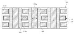
도 2a 내지 도 2e는 본 발명의 제 2 실시예에 따른 1-트랜지스터형 디램의 레이아웃을 도시한 도면이다. 여기서, 도 2a 내지 도 2e에 따른 제 2 실시예는 제 1 및 제 2 금속배선(212a, 212b)을 동시에 형성하는 하는 것이 아닌 라인 형태의 제 1 금속배선(212a)을 형성한 이후에 섬 형태의 제 2 금속배선(212b)을 형성하는 것이 제 1 실시예와 다르다.2A to 2E are diagrams showing the layout of the one-transistor DRAM according to the second embodiment of the present invention. Here, the second embodiment according to FIGS. 2A to 2E does not form the first and
도 2a에 도시된 바와 같이, 반도체 기판(200)에 활성영역(202)을 형성하여 소자분리막(204)을 정의한다.As shown in FIG. 2A, an
그 다음, 반도체 기판(200) 상부에 복수개의 워드라인(206)을 형성한다. 여기서, 워드라인(206)은 활성영역(202)과 소자분리막(204)을 동시에 가로지르며, 활성영역(202) 하나에 두 개의 워드라인(206)을 형성하는 것이 바람직하다.Next, a plurality of
그리고, 워드라인(206)은 셀 어레이 블럭(미도시)의 일측에 위치한 서브 워드라인(미도시) 부터 셀 어레이 블럭의 타측에 위치한 서브 워드라인(미도시) 까지 라인 형태로 형성하는 것이 바람직하다.The
그 다음, 워드라인(206) 양측벽에 게이트 스페이서(미도시)를 형성하고, 소스/드레인 이온 주입 공정을 수행하여 워드라인(206) 양측의 활성영역(202) 내에 소스 영역(208a) 및 드레인 영역(208b)을 형성한다.Next, gate spacers (not shown) are formed on both sidewalls of the
여기서, 소스 영역(208a)은 두 개의 워드라인(206) 사이의 활성영역(202) 내에 형성하고, 드레인 영역(208b)은 활성영역(202) 에지부 내에 형성하는 것이 바람직하다.Here, the
그 다음, 소스 및 드레인 영역(108a, 108b)과 각각 접속하는 복수개의 제 1 콘택플러그(210)를 형성한다. 여기서, 제 1 콘택플러그(210)는 일대일 대응하여 형성하고, 원형 형태 또는 타원형 형태로 형성하는 것이 바람직하다.Next, a plurality of first contact plugs 210 are formed to connect with the source and
그 다음, 도 2b에 도시된 바와 같이, 소스 영역(208a)에 접속되는 제 1 콘택플러그(210) 상부에 제 1 금속배선(212a)을 형성한다.Next, as shown in FIG. 2B, a
여기서, 제 1 금속배선(212a)은 소스 영역(208a)을 서로 연결하여 공통 소스로 사용하기 위해 형성하는 것으로, 워드라인(206)과 평행한 방향에서 양쪽의 워드라인(206)과 각각 10~100nm 만큼 중첩되도록 라인(line) 형태로 형성하는 것이 바람직하다.Here, the
그리고, 제 1 금속배선(212a)에는 트랜지스터 동작시 소스 영역(208a)에서 드레인 영역(208b)으로 전류 경로가 형성되도록 접지전압 VSS이 인가되는 것이 바람직하다.In addition, the ground voltage VSS is applied to the
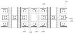
도 2c에 도시된 바와 같이, 드레인 영역(208b)에 접속되는 제 1 콘택플러그(210) 상부에 제 2 금속배선(212b)을 형성한다.As shown in FIG. 2C, a
여기서, 제 2 금속배선(212b)은 드레인 영역(208b) 상부에만 섬(island) 형태로 형성하는 것이 바람직하다. 그리고, 섬 형태는 직사각형 또는 정사각형인 것이 바람직하다.Here, the
그리고, 제 2 금속배선(212b)은 활성영역(202) 상의 워드라인(206)과 소자분리막(204) 상의 워드라인(206)에 각각 10~100nm 만큼 중첩되도록 형성하는 것이 바람직하다. 여기서, 활성영역(202) 상의 워드라인(206)에 중첩되는 폭과 소자분리막(204) 상의 워드라인(206)에 중첩되는 폭은 동일하거나 서로 다르게 형성할 수 있다.The
이와 같이, 제 1 금속배선(212a)을 형성한 후에 제 2 금속배선(212b)을 형성 함으로써 공정 마진의 부족으로 인해 제 2 금속배선(212b)의 모서리 부분이 과도 식각되어 제 2 금속배선(212b)의 크기가 작게 형성될 수 있는 것을 방지할 수 있다.As such, after the
도 2d에 도시된 바와 같이, 제 2 금속배선(212b) 상부에 제 2 콘택플러그(214)를 형성한다.As shown in FIG. 2D, a
여기서, 제 2 콘택플러그(214)는 후속 공정에서 형성될 비트라인과 드레인 영역(208b)을 접속시키기 위해 형성하는 것으로, 원형 형태 또는 타원형 형태로 형성하는 것이 바람직하다.Here, the
그리고, 제 2 콘택플러그(214)는 제 1 콘택플러그(210)과 축(on-axis) 형태를 이룰 수 있도록 제 1 콘택플러그(210)와 중첩하여 형성하는 것이 바람직하며, 제 2 금속배선(212b) 내에 형성하는 것이 바람직하다.In addition, the
도 1e에 도시된 바와 같이, 제 2 콘택플러그(214) 상부에 복수개의 비트라인(216)을 형성한다.As shown in FIG. 1E, a plurality of
여기서, 비트라인(216)은 워드라인(206) 및 제 1 금속배선(212a)과 수직한 방향으로 형성되며, 제 2 콘택플러그(214)와 중첩되도록 형성하는 것이 바람직하다.The
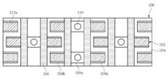
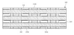
도 3a 내지 도 3e는 본 발명의 제 3 실시예에 따른 1-트랜지스터형 디램의 레이아웃을 도시한 도면이다. 여기서, 도 3a 내지 도 3e에 따른 제 3 실시예는 제 1 및 제 2 금속배선(312a, 312b)을 동시에 형성하는 하는 것이 아닌 섬 형태의 제 1 금속배선(312a)을 형성한 이후에 라인 형태의 제 2 금속배선(312b)을 형성하는 것이 제 1 실시예와 다르다.3A to 3E are diagrams showing the layout of the one-transistor DRAM according to the third embodiment of the present invention. Here, the third embodiment according to FIGS. 3A to 3E does not form the first and
도 3a에 도시된 바와 같이, 반도체 기판(300)에 활성영역(302)을 형성하여 소자분리막(304)을 정의한다.As shown in FIG. 3A, an
그 다음, 반도체 기판(300) 상부에 복수개의 워드라인(306)을 형성한다. 여기서, 워드라인(306)은 활성영역(302)과 소자분리막(304)을 동시에 가로지르며, 활성영역(302) 하나에 두 개의 워드라인(306)을 형성하는 것이 바람직하다.Next, a plurality of
그리고, 워드라인(306)은 셀 어레이 블럭(미도시)의 일측에 위치한 서브 워드라인(미도시) 부터 셀 어레이 블럭의 타측에 위치한 서브 워드라인(미도시) 까지 라인 형태로 형성하는 것이 바람직하다.The
그 다음, 워드라인(306) 양측벽에 게이트 스페이서(미도시)를 형성하고, 소스/드레인 이온 주입 공정을 수행하여 워드라인(306) 양측의 활성영역(302) 내에 소스 영역(308a) 및 드레인 영역(308b)을 형성한다.Next, gate spacers (not shown) are formed on both sidewalls of the
여기서, 소스 영역(308a)은 두 개의 워드라인(306) 사이의 활성영역(302) 내에 형성하고, 드레인 영역(308b)은 활성영역(302) 에지부 내에 형성하는 것이 바람직하다.Here, the
그 다음, 소스 및 드레인 영역(308a, 308b)과 각각 접속하는 복수개의 제 1 콘택플러그(310)를 형성한다. 여기서, 제 1 콘택플러그(310)는 일대일 대응하여 형성하고, 원형 형태 또는 타원형 형태로 형성하는 것이 바람직하다.Next, a plurality of first contact plugs 310 connected to the source and
그 다음, 도 3b에 도시된 바와 같이, 드레인 영역(308b)에 접속되는 제 1 콘택플러그(310) 상부에 제 1 금속배선(312a)을 형성한다.Next, as shown in FIG. 3B, a
여기서, 제 1 금속배선(312a)은 드레인 영역(308b) 상부에만 섬(island) 형태로 형성하는 것이 바람직하다. 그리고, 섬 형태는 직사각형 또는 정사각형인 것이 바람직하다.In this case, the
그리고, 제 1 금속배선(312a)은 활성영역(302) 상의 워드라인(306)과 소자분리막(304) 상의 워드라인(306)에 각각 10~100nm 만큼 중첩되도록 형성하는 것이 바람직하다. 여기서, 활성영역(302) 상의 워드라인(306)에 중첩되는 폭과 소자분리막(304) 상의 워드라인(306)에 중첩되는 폭은 동일하거나 서로 다르게 형성할 수 있다.The
도 3c에 도시된 바와 같이, 소스 영역(308a)에 접속되는 제 1 콘택플러그(310) 상부에 제 2 금속배선(312b)을 형성한다.As shown in FIG. 3C, a
여기서, 제 2 금속배선(312b)은 소스 영역(308a)을 서로 연결하여 공통 소스로 사용하기 위해 형성하는 것으로, 워드라인(306)과 평행한 방향에서 양쪽의 워드라인(306)과 각각 10~100nm 만큼 중첩되도록 라인(line) 형태로 형성하는 것이 바람직하다.Here, the
그리고, 제 2 금속배선(312b)에는 트랜지스터 동작시 소스 영역(308a)에서 드레인 영역(308b)으로 전류 경로가 형성되도록 접지전압 VSS이 인가되는 것이 바람직하다.In addition, the ground voltage VSS is applied to the
이와 같이, 제 1 금속배선(312a)을 형성한 후에 제 2 금속배선(312b)을 형성함으로써 공정 마진의 부족으로 인해 제 1 금속배선(312a)의 모서리 부분이 과도 식각되어 제 1 금속배선(312a)의 크기가 작게 형성될 수 있는 것을 방지할 수 있 다.As such, after the
도 3d에 도시된 바와 같이, 제 1 금속배선(312a) 상부에 제 2 콘택플러그(314)를 형성한다.As shown in FIG. 3D, a
여기서, 제 2 콘택플러그(314)는 후속 공정에서 형성될 비트라인과 드레인 영역(308b)을 접속시키기 위해 형성하는 것으로, 원형 형태 또는 타원형 형태로 형성하는 것이 바람직하다. 그리고, 제 2 콘택플러그(314)는 제 1 콘택플러그(310)과 축(on-axis) 형태를 이룰 수 있도록 제 1 콘택플러그(310)와 중첩하여 형성하는 것이 바람직하며, 제 1 금속배선(312a) 내에 형성하는 것이 바람직하다.In this case, the
도 3e에 도시된 바와 같이, 제 2 콘택플러그(314) 상부에 복수개의 비트라인(316)을 형성한다.As shown in FIG. 3E, a plurality of
여기서, 비트라인(316)은 워드라인(306) 및 제 2 금속배선(312b)과 수직한 방향으로 형성되며, 제 2 콘택플러그(314)와 중첩되도록 형성하는 것이 바람직하다.Here, the
도 1a 내지 도 1f는 본 발명의 제 1 실시예에 따른 1-트랜지스터형 디램의 레이아웃을 도시한 도면.1A to 1F show the layout of a one-transistor DRAM according to a first embodiment of the present invention.
도 2a 내지 도 2e는 본 발명의 제 2 실시예에 따른 1-트랜지스터형 디램의 레이아웃을 도시한 도면.2A to 2E show the layout of a one-transistor DRAM according to a second embodiment of the present invention.
도 3a 내지 도 3e는 본 발명의 제 3 실시예에 따른 1-트랜지스터형 디램의 레이아웃을 도시한 도면.3A to 3E show the layout of a one-transistor DRAM according to a third embodiment of the present invention.
Claims (11)
Translated fromKoreanPriority Applications (2)
| Application Number | Priority Date | Filing Date | Title |
|---|---|---|---|
| KR1020070104561AKR100900136B1 (en) | 2007-10-17 | 2007-10-17 | 1-transistor DRAM |
| US12/164,153US20090101981A1 (en) | 2007-10-17 | 2008-06-30 | One-transistor type dram |
Applications Claiming Priority (1)
| Application Number | Priority Date | Filing Date | Title |
|---|---|---|---|
| KR1020070104561AKR100900136B1 (en) | 2007-10-17 | 2007-10-17 | 1-transistor DRAM |
Publications (2)
| Publication Number | Publication Date |
|---|---|
| KR20090039110A KR20090039110A (en) | 2009-04-22 |
| KR100900136B1true KR100900136B1 (en) | 2009-06-01 |
Family
ID=40562611
Family Applications (1)
| Application Number | Title | Priority Date | Filing Date |
|---|---|---|---|
| KR1020070104561AExpired - Fee RelatedKR100900136B1 (en) | 2007-10-17 | 2007-10-17 | 1-transistor DRAM |
Country Status (2)
| Country | Link |
|---|---|
| US (1) | US20090101981A1 (en) |
| KR (1) | KR100900136B1 (en) |
Citations (4)
| Publication number | Priority date | Publication date | Assignee | Title |
|---|---|---|---|---|
| KR20030002203A (en)* | 2001-06-30 | 2003-01-08 | 주식회사 하이닉스반도체 | Semiconductor DRAM cell |
| KR20060001489A (en)* | 2004-06-30 | 2006-01-06 | 주식회사 하이닉스반도체 | Semiconductor device |
| KR20060016312A (en)* | 2004-08-17 | 2006-02-22 | 삼성전자주식회사 | Phase change memory device and manufacturing method thereof |
| KR100699890B1 (en) | 2006-01-10 | 2007-03-28 | 삼성전자주식회사 | Semiconductor memory device and manufacturing method thereof |
Family Cites Families (5)
| Publication number | Priority date | Publication date | Assignee | Title |
|---|---|---|---|---|
| JP3068426B2 (en)* | 1994-12-21 | 2000-07-24 | 日本電気株式会社 | Semiconductor storage device |
| JPH10144886A (en)* | 1996-09-11 | 1998-05-29 | Toshiba Corp | Semiconductor device and manufacturing method thereof |
| TWI230392B (en)* | 2001-06-18 | 2005-04-01 | Innovative Silicon Sa | Semiconductor device |
| DE602005009793D1 (en)* | 2005-01-21 | 2008-10-30 | St Microelectronics Srl | Phase change memory device and method for its production |
| JP4469744B2 (en)* | 2005-03-18 | 2010-05-26 | 株式会社東芝 | Semiconductor memory device and driving method of semiconductor memory device |
- 2007
- 2007-10-17KRKR1020070104561Apatent/KR100900136B1/ennot_activeExpired - Fee Related
- 2008
- 2008-06-30USUS12/164,153patent/US20090101981A1/ennot_activeAbandoned
Patent Citations (4)
| Publication number | Priority date | Publication date | Assignee | Title |
|---|---|---|---|---|
| KR20030002203A (en)* | 2001-06-30 | 2003-01-08 | 주식회사 하이닉스반도체 | Semiconductor DRAM cell |
| KR20060001489A (en)* | 2004-06-30 | 2006-01-06 | 주식회사 하이닉스반도체 | Semiconductor device |
| KR20060016312A (en)* | 2004-08-17 | 2006-02-22 | 삼성전자주식회사 | Phase change memory device and manufacturing method thereof |
| KR100699890B1 (en) | 2006-01-10 | 2007-03-28 | 삼성전자주식회사 | Semiconductor memory device and manufacturing method thereof |
Also Published As
| Publication number | Publication date |
|---|---|
| KR20090039110A (en) | 2009-04-22 |
| US20090101981A1 (en) | 2009-04-23 |
Similar Documents
| Publication | Publication Date | Title |
|---|---|---|
| TWI766448B (en) | Memory device and manufacturing method of memory device | |
| CN109979941B (en) | Semiconductor memory device with a memory cell having a memory cell with a memory cell having a memory cell | |
| US11557677B2 (en) | Integrated circuit device and method of manufacturing the same | |
| US7139184B2 (en) | Memory cell array | |
| CN101208795B (en) | Trench isolation transistor with grounded gate for 4.5F2 dynamic random access memory cell and method of manufacturing same | |
| JP5614915B2 (en) | Semiconductor device, semiconductor device manufacturing method, and data processing system | |
| US20080017904A1 (en) | Semiconductor device | |
| JPH05218348A (en) | Return-type bit line strucutre and its manufacture | |
| KR100683295B1 (en) | Layout and Wiring Design of Memory Cells with Vertical Transistors | |
| US10103101B2 (en) | Semiconductor device and method of manufacturing the same | |
| KR100471183B1 (en) | Semiconductor memory device having offset transistor and method of fabricating the same | |
| US6882556B2 (en) | Semiconductor memory having a configuration of memory cells | |
| US6911687B1 (en) | Buried bit line-field isolation defined active semiconductor areas | |
| KR100900136B1 (en) | 1-transistor DRAM | |
| JP2011029258A (en) | Semiconductor memory device | |
| CN114171079A (en) | Integrated circuit device | |
| US6849893B2 (en) | Semiconductor circuit structure and method for fabricating the semiconductor circuit structure | |
| US20240260251A1 (en) | Memory Circuitry And Methods Used In Forming Memory Circuitry | |
| TWI865000B (en) | Semiconductor devices and memory devices | |
| WO2024036877A1 (en) | Semiconductor structure and method for forming same | |
| KR20040040691A (en) | Semiconductor memory device having staircase vertical transistor and method of fabricating the same | |
| KR20100007480A (en) | High integrated semiconductor memory device | |
| KR20120033510A (en) | Semiconductor intergrated circuit |
Legal Events
| Date | Code | Title | Description |
|---|---|---|---|
| A201 | Request for examination | ||
| PA0109 | Patent application | St.27 status event code:A-0-1-A10-A12-nap-PA0109 | |
| PA0201 | Request for examination | St.27 status event code:A-1-2-D10-D11-exm-PA0201 | |
| D13-X000 | Search requested | St.27 status event code:A-1-2-D10-D13-srh-X000 | |
| D14-X000 | Search report completed | St.27 status event code:A-1-2-D10-D14-srh-X000 | |
| E902 | Notification of reason for refusal | ||
| PE0902 | Notice of grounds for rejection | St.27 status event code:A-1-2-D10-D21-exm-PE0902 | |
| P11-X000 | Amendment of application requested | St.27 status event code:A-2-2-P10-P11-nap-X000 | |
| P13-X000 | Application amended | St.27 status event code:A-2-2-P10-P13-nap-X000 | |
| PG1501 | Laying open of application | St.27 status event code:A-1-1-Q10-Q12-nap-PG1501 | |
| E701 | Decision to grant or registration of patent right | ||
| PE0701 | Decision of registration | St.27 status event code:A-1-2-D10-D22-exm-PE0701 | |
| GRNT | Written decision to grant | ||
| PR0701 | Registration of establishment | St.27 status event code:A-2-4-F10-F11-exm-PR0701 | |
| PR1002 | Payment of registration fee | St.27 status event code:A-2-2-U10-U11-oth-PR1002 Fee payment year number:1 | |
| PG1601 | Publication of registration | St.27 status event code:A-4-4-Q10-Q13-nap-PG1601 | |
| PN2301 | Change of applicant | St.27 status event code:A-5-5-R10-R13-asn-PN2301 St.27 status event code:A-5-5-R10-R11-asn-PN2301 | |
| LAPS | Lapse due to unpaid annual fee | ||
| PC1903 | Unpaid annual fee | St.27 status event code:A-4-4-U10-U13-oth-PC1903 Not in force date:20120523 Payment event data comment text:Termination Category : DEFAULT_OF_REGISTRATION_FEE | |
| PN2301 | Change of applicant | St.27 status event code:A-5-5-R10-R13-asn-PN2301 St.27 status event code:A-5-5-R10-R11-asn-PN2301 | |
| PC1903 | Unpaid annual fee | St.27 status event code:N-4-6-H10-H13-oth-PC1903 Ip right cessation event data comment text:Termination Category : DEFAULT_OF_REGISTRATION_FEE Not in force date:20120523 | |
| PN2301 | Change of applicant | St.27 status event code:A-5-5-R10-R13-asn-PN2301 St.27 status event code:A-5-5-R10-R11-asn-PN2301 | |
| P22-X000 | Classification modified | St.27 status event code:A-4-4-P10-P22-nap-X000 |