KR100897826B1 - Manufacturing Method of Semiconductor Device - Google Patents
Manufacturing Method of Semiconductor DeviceDownload PDFInfo
- Publication number
- KR100897826B1 KR100897826B1KR1020070088470AKR20070088470AKR100897826B1KR 100897826 B1KR100897826 B1KR 100897826B1KR 1020070088470 AKR1020070088470 AKR 1020070088470AKR 20070088470 AKR20070088470 AKR 20070088470AKR 100897826 B1KR100897826 B1KR 100897826B1
- Authority
- KR
- South Korea
- Prior art keywords
- insulating film
- protective insulating
- semiconductor device
- manufacturing
- copper
- Prior art date
- Legal status (The legal status is an assumption and is not a legal conclusion. Google has not performed a legal analysis and makes no representation as to the accuracy of the status listed.)
- Expired - Fee Related
Links
Images


Classifications
- H—ELECTRICITY
- H01—ELECTRIC ELEMENTS
- H01L—SEMICONDUCTOR DEVICES NOT COVERED BY CLASS H10
- H01L21/00—Processes or apparatus adapted for the manufacture or treatment of semiconductor or solid state devices or of parts thereof
- H01L21/02—Manufacture or treatment of semiconductor devices or of parts thereof
- H01L21/04—Manufacture or treatment of semiconductor devices or of parts thereof the devices having potential barriers, e.g. a PN junction, depletion layer or carrier concentration layer
- H01L21/18—Manufacture or treatment of semiconductor devices or of parts thereof the devices having potential barriers, e.g. a PN junction, depletion layer or carrier concentration layer the devices having semiconductor bodies comprising elements of Group IV of the Periodic Table or AIIIBV compounds with or without impurities, e.g. doping materials
- H01L21/28—Manufacture of electrodes on semiconductor bodies using processes or apparatus not provided for in groups H01L21/20 - H01L21/268
- H—ELECTRICITY
- H01—ELECTRIC ELEMENTS
- H01L—SEMICONDUCTOR DEVICES NOT COVERED BY CLASS H10
- H01L21/00—Processes or apparatus adapted for the manufacture or treatment of semiconductor or solid state devices or of parts thereof
- H01L21/70—Manufacture or treatment of devices consisting of a plurality of solid state components formed in or on a common substrate or of parts thereof; Manufacture of integrated circuit devices or of parts thereof
- H01L21/71—Manufacture of specific parts of devices defined in group H01L21/70
- H01L21/768—Applying interconnections to be used for carrying current between separate components within a device comprising conductors and dielectrics
- H01L21/76838—Applying interconnections to be used for carrying current between separate components within a device comprising conductors and dielectrics characterised by the formation and the after-treatment of the conductors
- H01L21/7684—Smoothing; Planarisation
- H—ELECTRICITY
- H01—ELECTRIC ELEMENTS
- H01L—SEMICONDUCTOR DEVICES NOT COVERED BY CLASS H10
- H01L21/00—Processes or apparatus adapted for the manufacture or treatment of semiconductor or solid state devices or of parts thereof
- H01L21/02—Manufacture or treatment of semiconductor devices or of parts thereof
- H01L21/02041—Cleaning
- H01L21/02057—Cleaning during device manufacture
- H01L21/02068—Cleaning during device manufacture during, before or after processing of conductive layers, e.g. polysilicon or amorphous silicon layers
- H01L21/02074—Cleaning during device manufacture during, before or after processing of conductive layers, e.g. polysilicon or amorphous silicon layers the processing being a planarization of conductive layers
- H—ELECTRICITY
- H01—ELECTRIC ELEMENTS
- H01L—SEMICONDUCTOR DEVICES NOT COVERED BY CLASS H10
- H01L21/00—Processes or apparatus adapted for the manufacture or treatment of semiconductor or solid state devices or of parts thereof
- H01L21/70—Manufacture or treatment of devices consisting of a plurality of solid state components formed in or on a common substrate or of parts thereof; Manufacture of integrated circuit devices or of parts thereof
- H01L21/71—Manufacture of specific parts of devices defined in group H01L21/70
- H01L21/768—Applying interconnections to be used for carrying current between separate components within a device comprising conductors and dielectrics
- H01L21/76801—Applying interconnections to be used for carrying current between separate components within a device comprising conductors and dielectrics characterised by the formation and the after-treatment of the dielectrics, e.g. smoothing
- H01L21/76829—Applying interconnections to be used for carrying current between separate components within a device comprising conductors and dielectrics characterised by the formation and the after-treatment of the dielectrics, e.g. smoothing characterised by the formation of thin functional dielectric layers, e.g. dielectric etch-stop, barrier, capping or liner layers
- H01L21/76834—Applying interconnections to be used for carrying current between separate components within a device comprising conductors and dielectrics characterised by the formation and the after-treatment of the dielectrics, e.g. smoothing characterised by the formation of thin functional dielectric layers, e.g. dielectric etch-stop, barrier, capping or liner layers formation of thin insulating films on the sidewalls or on top of conductors
- H—ELECTRICITY
- H01—ELECTRIC ELEMENTS
- H01L—SEMICONDUCTOR DEVICES NOT COVERED BY CLASS H10
- H01L21/00—Processes or apparatus adapted for the manufacture or treatment of semiconductor or solid state devices or of parts thereof
- H01L21/70—Manufacture or treatment of devices consisting of a plurality of solid state components formed in or on a common substrate or of parts thereof; Manufacture of integrated circuit devices or of parts thereof
- H01L21/71—Manufacture of specific parts of devices defined in group H01L21/70
- H01L21/768—Applying interconnections to be used for carrying current between separate components within a device comprising conductors and dielectrics
- H01L21/76838—Applying interconnections to be used for carrying current between separate components within a device comprising conductors and dielectrics characterised by the formation and the after-treatment of the conductors
- H01L21/76877—Filling of holes, grooves or trenches, e.g. vias, with conductive material
- H01L21/76883—Post-treatment or after-treatment of the conductive material
Landscapes
- Engineering & Computer Science (AREA)
- Physics & Mathematics (AREA)
- Condensed Matter Physics & Semiconductors (AREA)
- General Physics & Mathematics (AREA)
- Manufacturing & Machinery (AREA)
- Computer Hardware Design (AREA)
- Microelectronics & Electronic Packaging (AREA)
- Power Engineering (AREA)
- Internal Circuitry In Semiconductor Integrated Circuit Devices (AREA)
Abstract
Translated fromKoreanDescription
Translated fromKorean본 발명은 반도체 소자의 제조방법에 관한 것으로서, 특히 힐록(hillock)과 보이드(void)를 최소화시킬 수 있는 반도체 소자의 제조방법에 관한 것이다.The present invention relates to a method for manufacturing a semiconductor device, and more particularly, to a method for manufacturing a semiconductor device capable of minimizing hillock and void.
일반적으로, 반도체 소자의 금속배선으로 널리 사용하는 금속으로 알루미늄(Al), 알루미늄 합금 및 텅스텐(W) 등이 있다.Generally, metals widely used as metal wirings of semiconductor devices include aluminum (Al), aluminum alloys, and tungsten (W).
그러나, 이러한 금속들은 반도체 소자가 고집적화됨에 따라 낮은 융점과 높은 비저항으로 인하여 초고집적 반도체 소자에 더 이상 적용이 어렵게 되었다.However, these metals are no longer applicable to ultra-high density semiconductor devices due to the low melting point and high resistivity as semiconductor devices are highly integrated.
따라서, 금속배선의 대체 재료에 대한 개발 필요성이 대두되고 있는 실정이다. 대체 재료로 전도성이 우수한 물질인 구리(Cu), 금(Au), 은(Ag), 코발트(Co), 크롬(Cr), 니켈(Ni) 등이 있으며, 이러한 물질들 중 비저항이 작고, 일렉트로 마이그레이션(electro migration ; EM)과 스트레스 마이그레이션(stress migration; SM) 등의 신뢰성이 우수하며, 생산원가가 저렴한 구리 및 구리 합금이 널리 적용되고 있는 추세이다.Therefore, there is a need for development of alternative materials for metal wiring. Alternative materials include copper (Cu), gold (Au), silver (Ag), cobalt (Co), chromium (Cr), and nickel (Ni), which are highly conductive materials. Copper and copper alloys with high reliability and low production cost, such as electro migration (EM) and stress migration (SM), are widely applied.
종래의 구리배선은 알루미늄보다 고유저항(resistivity)을 갖고 있어 RC 시간 지연을 줄일 수 있으므로, 0.13㎛이하의 디자인 룰(design rule)을 갖는 소자에 서 사용하게 되었다.Conventional copper wiring has a resistivity higher than that of aluminum, and thus, RC time delay can be reduced. Therefore, the copper wiring has been used in devices having a design rule of 0.13 µm or less.
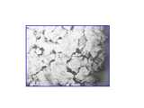
그런데 구리배선의 열팽창 계수는 유전체막(dielectric film)보다 10배정도 큰 값을 가지며, 반도체 공정에서 사용되는 어느 특정한 온도 이상에서 급격한 팽창을 하게 된다. 이로 인해 압축 스트레스(compressive stress)가 쌓이게 되는데, 이것이 크면 스트레스 완화를 위하여 구리배선 상에 작은 언덕 같은 모양들이 다수 발생하는 힐록(hillock)이 형성된다. 따라서, 도 1에 도시된 바와 같이 힐록에 의해 화학 기계적 연마(Chemical Mechanical Polishing: CMP) 공정 후 금속배선의 잔여물이 남게 되며, 이러한 잔여물은 배선 간의 단락 및 보이드의 주요 원인이 되기 때문에 공정 신뢰성(reliability)에 영향을 주게 된다.However, the thermal expansion coefficient of the copper wiring is about 10 times larger than that of the dielectric film, and the thermal expansion is rapidly expanded at a certain temperature or more used in the semiconductor process. This builds up compressive stress, which is large, creating a hillock with many small hill-like shapes on the copper wiring to relieve stress. Therefore, as shown in FIG. 1, the residue of the metal wiring remains after the chemical mechanical polishing (CMP) process by Hillock, and the process reliability is a major cause of short circuits and voids between the wirings. will affect reliability.
따라서, 상기와 같은 문제점을 해결하기 위하여, 본 발명은 힐록(hillock)과 보이드(void)를 최소화시킬 수 있는 반도체 소자의 제조방법을 제공하는 데 그 목적이 있다.Accordingly, in order to solve the above problems, an object of the present invention is to provide a method of manufacturing a semiconductor device capable of minimizing hillocks and voids.
상기와 같은 목적을 달성하기 위한 본 발명에 따른 반도체 소자의 제조방법은 화학적 기계적 연마를 통해 평탄화된 제 1 베리어 메탈층과 제 1 구리 배선층을 갖는 다중 보호절연막 구조의 층간절연막에 NH3 처리 공정을 복수의 단계로 나누어서 각 시간 별로 일정한 기간을 두고 진행하는 단계; 상기 제 1 구리 배선층을 포함한 다중 보호절연막 구조의 층간절연막 상에 구리 확산 방지용 캡핑막을 형성하는 단계; 상기 구리 확산 방지용 캡핑막을 화학적 기계적 연마를 통해 평탄화하는 단계를 포함하며, 상기 구리 확산 방지용 캡핑막은 상기 제 1 구리배선층에 발생하는 힐록의 두께가 포화상태가 일어나는 시점까지 그 두께가 커지도록 형성되는 것을 특징으로 한다.The semiconductor device manufacturing method according to the present invention for achieving the above object is a plurality of NH3 treatment process in the interlayer insulating film of the multi-layer protective insulating film structure having the first barrier metal layer and the first copper wiring layer planarized by chemical mechanical polishing. Dividing into steps of proceeding with a certain period for each time; Forming a copper diffusion preventing capping film on the interlayer insulating film of the multiple protective insulating film structure including the first copper wiring layer; And planarizing the copper diffusion preventing capping film through chemical mechanical polishing, wherein the copper diffusion preventing capping film is formed such that the thickness of the hillock generated in the first copper wiring layer is increased until the saturation state occurs. It features.
이상에서 설명한 바와 같이 본 발명에 의한 반도체 소자의 제조방법은 다음과 같은 효과가 있다.As described above, the method for manufacturing a semiconductor device according to the present invention has the following effects.
첫째, NH3 플라즈마 처리 공정을 2단계 또는 3단계 등 복수의 단계로 나누어서 진행시킴으로써 구리배선의 힐록을 최소화할 수 있다.First, it is possible to minimize the hillock of the copper wiring by dividing the NH3 plasma treatment process into a plurality of stages such as two or three stages.
둘째, 구리 배선 위에 증착되는 구리 확산 방지용 캡핑막의 두께를 구리 배선의 힐록 두께가 포화될만큼 키워준 다음 CMP 공정을 통해 평탄화시켜 IDL 층 증착시 열공급에 의해 힐록 두께를 최소화시킴으로써 베리어 메탈층의 잔여물에 의한 배선의 단락을 줄일 수 있다.Second, the thickness of the copper diffusion preventing capping film deposited on the copper wiring is increased to the saturation of the hillock thickness of the copper wiring, and then planarized through the CMP process to minimize the hillock thickness by heat supply when depositing the IDL layer. The short circuit of the wiring can be reduced.
셋째, 콘택홀의 힐록 두께를 억제시킴으로써 보이드 유발을 방지할 수 있다.Third, voids can be prevented by suppressing the hillock thickness of the contact hole.
이하, 첨부된 도면을 참고하여 본 발명에 의한 반도체 소자의 제조방법에 관하여 상세히 설명하기로 한다.Hereinafter, a method of manufacturing a semiconductor device according to the present invention will be described in detail with reference to the accompanying drawings.
도 2a 내지 도 2e는 본 발명에 따른 반도체 소자의 제조방법을 나타낸 공정단면도이다.2A through 2E are cross-sectional views illustrating a method of manufacturing a semiconductor device in accordance with the present invention.
도 2a에 도시된 바와 같이, 먼저 반도체 기판(90) 위에 제 1 보호절연막(100)을 증착하고, 콘택홀을 형성하기 위한 포토레지스트를 형성하는 노광공정을 수행한다. 여기서, 제 1 보호절연막(100)은 SiH4로 형성될 수 있다.As shown in FIG. 2A, first, a first
노광공정은 반도체 기판(90) 상에 도포된 포토레지스트막에 대해 소정의 노광 마스크(미도시)를 이용하여 노광장비에서 노광처리가 수행되고 베이킹 장비에서 베이킹 처리되며 소정의 현상액을 이용하여 노광처리된 포토레지스트막을 제거하여 포토레지스트를 형성한다.The exposure process is performed by an exposure apparatus on a photoresist film applied on a
노광공정 이후, 포토레지스트를 마스크로 소정의 건식식각에 의해 제 1 보호절연막(100)을 식각함으로써 콘택홀을 형성하고, 콘택홀 내부에 텅스텐 플러그(110)를 형성한다.After the exposure process, a contact hole is formed by etching the first
다음으로, 도 2b에 도시된 바와 같이, 텅스텐 플러그(110)를 포함한 제 1 보호절연막(100) 상에 제 2 보호절연막(120)과 제 3 보호절연막(130)을 순차적으로 증착한다. 여기서 제 2 보호절연막(120)은 FSG로 형성될 수 있고, 제 3 보호절연막(130)은 SiH4로 형성될 수 있다.Next, as shown in FIG. 2B, the second protective
증착한 후, 트렌치를 형성하기 위한 포토레지스트를 형성하는 노광공정을 수행한다. 이러한 포토레지스트를 마스크로 소정의 건식식각에 의해 제 2 보호절연막(120)과 제 3 보호절연막(130)의 일부를 식각함으로써 트렌치를 형성한다.After deposition, an exposure process for forming a photoresist for forming trenches is performed. A trench is formed by etching part of the second protective
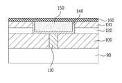
이어서, 도 2c에 도시된 바와 같이, 포토레지스트를 제거한 후, 트렌치를 포함한 반도체 기판의 전면에 제 1 베리어 메탈(140)와 제 1 구리 배선층(150)을 형성하고 제 3 보호절연막(130)의 표면이 노출되도록 제 1 구리 배선층(150)을 화학 기계적 연마(CMP: Chemical Mechanical Polishing)를 통해 평탄화시킨다. 여기서, 제 1 베리어 메탈(140)은 Ta/TaN으로 형성할 수 있다.Subsequently, as shown in FIG. 2C, after the photoresist is removed, the
이후, 노출된 제 1 구리 배선층(150) 상에 형성된 CuO(Cupric Oxide)를 환원 시켜 순수한 구리 상태로 만들어 주기 위해 NH3 처리 공정을 복수의 단계로 나누어서 진행한다. 여기서 NH3 처리 공정은 예를 들어 2단계(7초/8초) 또는 3단계(5초/5초/5초)로 나누어서 각 시간 별로 일정한 기간을 두고 진행하며, 이로 인해 제 1 구리 배선층(150)의 표면에 발생하는 힐록의 두께를 최소화할 수 있다.Subsequently, in order to reduce CuO (Cupric Oxide) formed on the exposed first
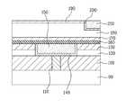
다음으로, 도 2d에 도시된 바와 같이, 제 1 구리 배선층(150)을 포함한 반도체 기판의 전면에 구리 확산 방지용 캡핑막(160)을 형성한다. 여기서, 구리 확산 방지용 캡핑막(160)은 SiC, SiCN 및 SiOF를 이용하여 형성할 수 있으며, 350~400℃의 온도에서 형성할 수 있다. 또한, 그 두께는 힐록의 두께의 포화상태가 일어나는 시점까지 커지게 할 수 있다. 이어서, 구리 확산 방지용 캡핑막(160)을 화학 기계적 연마를 통해 평탄화시킨다.Next, as shown in FIG. 2D, a copper diffusion preventing
다음으로, 도 2e에 도시된 바와 같이, 구리 확산 방지용 캡핑막(160) 상에 제 4 보호절연막(170), 제 5 보호절연막(180) 및 제 6 보호절연막(190)을 순차적으로 증착한다. 그리고, 노광 및 식각공정을 통해 제 5 보호절연막(180) 및 제 6 보호절연막(190)을 식각함으로써 트렌치를 형성하고, 트렌치를 포함한 제 6 보호절연막(190) 전면에 제 2 베리어 메탈(200)와 제 2 구리 배선층(210)을 형성한다. 여기서, 제 4 보호절연막(170)과 제 6 보호절연막(190)은 SiH4로 형성할 수 있고, 제 5 보호절연막(200)은 FSG로 형성할 수 있다.Next, as shown in FIG. 2E, the fourth protective
이와 같이, 구리 확산 방지용 캡핑막(160)의 두께를 구리 배선(120)의 힐록 두께가 포화될만큼 키워준 다음 CMP 공정을 통해 평탄화시켜 제 4 보호절연막(170), 제 5 보호절연막(180) 및 제 6 보호절연막(190)을 증착시 열공급에 의해 힐록 두께를 최소화시킴으로써 제 1 베리어 메탈층(140)의 잔여물에 의한 배선의 단락을 줄일 수 있다. 또한, 힐록의 두께를 조절함으로써 보이드의 발생을 방지할 수 있다.As such, the thickness of the copper diffusion preventing
도 1은 종래의 반도체 소자의 제조공정 시 발생하는 힐록을 나타내는 도면.BRIEF DESCRIPTION OF THE DRAWINGS Fig. 1 is a view showing hillocks generated during a manufacturing process of a conventional semiconductor device.
도 2a 내지 도 2e는 본 발명에 따른 반도체 소자의 제조방법을 나타낸 공정단면도.2A through 2E are cross-sectional views illustrating a method of manufacturing a semiconductor device in accordance with the present invention.
* 도면의 주요 부분에 대한 부호의 설명 *Explanation of symbols on the main parts of the drawings
90: 반도체 기판100: 제 1 보호절연막90: semiconductor substrate 100: first protective insulating film
110: 텅스텐 플러그120: 제 2 보호절연막110: tungsten plug 120: second protective insulating film
130: 제 3 보호절연막140: 제 1 베리어 메탈층130: third protective insulating film 140: first barrier metal layer
150: 제 1 구리 배선층160: 구리 확산 방지용 캡핑막150: first copper wiring layer 160: copper diffusion preventing capping film
170: 제 4 보호절연막180: 제 5 보호절연막170: fourth protective insulating film 180: fifth protective insulating film
190: 제 6 보호절연막200: 제 2 베리어 메탈층190: sixth protective insulating film 200: second barrier metal layer
210: 제 2 구리 배선층210: second copper wiring layer
Claims (7)
Translated fromKoreanPriority Applications (2)
| Application Number | Priority Date | Filing Date | Title |
|---|---|---|---|
| KR1020070088470AKR100897826B1 (en) | 2007-08-31 | 2007-08-31 | Manufacturing Method of Semiconductor Device |
| US12/194,568US20090061616A1 (en) | 2007-08-31 | 2008-08-20 | Method for fabricating semiconductor device |
Applications Claiming Priority (1)
| Application Number | Priority Date | Filing Date | Title |
|---|---|---|---|
| KR1020070088470AKR100897826B1 (en) | 2007-08-31 | 2007-08-31 | Manufacturing Method of Semiconductor Device |
Publications (2)
| Publication Number | Publication Date |
|---|---|
| KR20090022826A KR20090022826A (en) | 2009-03-04 |
| KR100897826B1true KR100897826B1 (en) | 2009-05-18 |
Family
ID=40408144
Family Applications (1)
| Application Number | Title | Priority Date | Filing Date |
|---|---|---|---|
| KR1020070088470AExpired - Fee RelatedKR100897826B1 (en) | 2007-08-31 | 2007-08-31 | Manufacturing Method of Semiconductor Device |
Country Status (2)
| Country | Link |
|---|---|
| US (1) | US20090061616A1 (en) |
| KR (1) | KR100897826B1 (en) |
Families Citing this family (1)
| Publication number | Priority date | Publication date | Assignee | Title |
|---|---|---|---|---|
| US20130113103A1 (en)* | 2011-11-03 | 2013-05-09 | Texas Instruments Incorporated | DEVICE HAVING TSVs WITH GETTERING LAYER LATERAL TO TSV TIPS |
Citations (3)
| Publication number | Priority date | Publication date | Assignee | Title |
|---|---|---|---|---|
| KR20010107568A (en)* | 2000-05-24 | 2001-12-07 | 무라세 하루오 | Semiconductor device and method of manufacturing the same |
| KR20030051359A (en)* | 2001-12-18 | 2003-06-25 | 가부시키가이샤 히타치세이사쿠쇼 | Semiconductor device and method for manufacturing the same |
| KR100685138B1 (en) | 2005-10-25 | 2007-02-22 | 동부일렉트로닉스 주식회사 | Metal wiring formation method of semiconductor device |
Family Cites Families (5)
| Publication number | Priority date | Publication date | Assignee | Title |
|---|---|---|---|---|
| US6340435B1 (en)* | 1998-02-11 | 2002-01-22 | Applied Materials, Inc. | Integrated low K dielectrics and etch stops |
| US6255233B1 (en)* | 1998-12-30 | 2001-07-03 | Intel Corporation | In-situ silicon nitride and silicon based oxide deposition with graded interface for damascene application |
| US6368967B1 (en)* | 2000-05-04 | 2002-04-09 | Advanced Micro Devices, Inc. | Method to control mechanical stress of copper interconnect line using post-plating copper anneal |
| US7068138B2 (en)* | 2004-01-29 | 2006-06-27 | International Business Machines Corporation | High Q factor integrated circuit inductor |
| US7332428B2 (en)* | 2005-02-28 | 2008-02-19 | Infineon Technologies Ag | Metal interconnect structure and method |
- 2007
- 2007-08-31KRKR1020070088470Apatent/KR100897826B1/ennot_activeExpired - Fee Related
- 2008
- 2008-08-20USUS12/194,568patent/US20090061616A1/ennot_activeAbandoned
Patent Citations (3)
| Publication number | Priority date | Publication date | Assignee | Title |
|---|---|---|---|---|
| KR20010107568A (en)* | 2000-05-24 | 2001-12-07 | 무라세 하루오 | Semiconductor device and method of manufacturing the same |
| KR20030051359A (en)* | 2001-12-18 | 2003-06-25 | 가부시키가이샤 히타치세이사쿠쇼 | Semiconductor device and method for manufacturing the same |
| KR100685138B1 (en) | 2005-10-25 | 2007-02-22 | 동부일렉트로닉스 주식회사 | Metal wiring formation method of semiconductor device |
Also Published As
| Publication number | Publication date |
|---|---|
| US20090061616A1 (en) | 2009-03-05 |
| KR20090022826A (en) | 2009-03-04 |
Similar Documents
| Publication | Publication Date | Title |
|---|---|---|
| US20200090994A1 (en) | Semiconductor device with reduced via resistance | |
| JP4918778B2 (en) | Manufacturing method of semiconductor integrated circuit device | |
| CN101390204B (en) | Novel structures and methods for metal integration | |
| US20170110369A1 (en) | Electronic device and method for producing same | |
| US7651941B2 (en) | Method of manufacturing a semiconductor device that includes forming a via hole through a reaction layer formed between a conductive barrier and a wiring | |
| US10643887B2 (en) | Method of manufacturing damascene thin-film resistor (TFR) in poly-metal dielectric | |
| CN101740547B (en) | Semiconductor device and method of manufacturing semiconductor device, target of sputtering device | |
| KR100897826B1 (en) | Manufacturing Method of Semiconductor Device | |
| KR20100011799A (en) | Method of manufacturing semiconductor device | |
| JP4219215B2 (en) | Manufacturing method of electronic device | |
| KR101107229B1 (en) | Metal wiring formation method of semiconductor device | |
| KR100945503B1 (en) | Metal wiring formation method of semiconductor device | |
| KR100853800B1 (en) | Dual damascene pattern formation method of semiconductor device | |
| KR20090075501A (en) | Metal wiring of semiconductor device and method of forming the same | |
| JP4525534B2 (en) | Manufacturing method of semiconductor device | |
| KR100545196B1 (en) | Method for forming metal line of semiconductor device | |
| KR20100036008A (en) | Method for forming metal wiring of semiconductor device | |
| KR100808794B1 (en) | Manufacturing Method of Semiconductor Device | |
| KR101138063B1 (en) | Metal wiring formation method of semiconductor device | |
| KR20000043052A (en) | Metal wiring formation method of semiconductor device | |
| KR100705008B1 (en) | Method for manufacturing metal wiring of semiconductor device | |
| KR100920040B1 (en) | Wiring of a semiconductor device and its formation method | |
| KR20100073779A (en) | Metal line of semiconductor device and fabricating method thereof | |
| KR100720530B1 (en) | Metal wiring of semiconductor device and forming method thereof | |
| KR100458588B1 (en) | Fabrication method of semiconductor device |
Legal Events
| Date | Code | Title | Description |
|---|---|---|---|
| A201 | Request for examination | ||
| PA0109 | Patent application | St.27 status event code:A-0-1-A10-A12-nap-PA0109 | |
| PA0201 | Request for examination | St.27 status event code:A-1-2-D10-D11-exm-PA0201 | |
| PN2301 | Change of applicant | St.27 status event code:A-3-3-R10-R13-asn-PN2301 St.27 status event code:A-3-3-R10-R11-asn-PN2301 | |
| E902 | Notification of reason for refusal | ||
| PE0902 | Notice of grounds for rejection | St.27 status event code:A-1-2-D10-D21-exm-PE0902 | |
| AMND | Amendment | ||
| P11-X000 | Amendment of application requested | St.27 status event code:A-2-2-P10-P11-nap-X000 | |
| P13-X000 | Application amended | St.27 status event code:A-2-2-P10-P13-nap-X000 | |
| E601 | Decision to refuse application | ||
| PE0601 | Decision on rejection of patent | St.27 status event code:N-2-6-B10-B15-exm-PE0601 | |
| AMND | Amendment | ||
| E13-X000 | Pre-grant limitation requested | St.27 status event code:A-2-3-E10-E13-lim-X000 | |
| J201 | Request for trial against refusal decision | ||
| P11-X000 | Amendment of application requested | St.27 status event code:A-2-2-P10-P11-nap-X000 | |
| P13-X000 | Application amended | St.27 status event code:A-2-2-P10-P13-nap-X000 | |
| PJ0201 | Trial against decision of rejection | St.27 status event code:A-3-3-V10-V11-apl-PJ0201 | |
| PG1501 | Laying open of application | St.27 status event code:A-1-1-Q10-Q12-nap-PG1501 | |
| PB0901 | Examination by re-examination before a trial | St.27 status event code:A-6-3-E10-E12-rex-PB0901 | |
| B701 | Decision to grant | ||
| PB0701 | Decision of registration after re-examination before a trial | St.27 status event code:A-3-4-F10-F13-rex-PB0701 | |
| GRNT | Written decision to grant | ||
| PR0701 | Registration of establishment | St.27 status event code:A-2-4-F10-F11-exm-PR0701 | |
| PR1002 | Payment of registration fee | St.27 status event code:A-2-2-U10-U11-oth-PR1002 Fee payment year number:1 | |
| PG1601 | Publication of registration | St.27 status event code:A-4-4-Q10-Q13-nap-PG1601 | |
| FPAY | Annual fee payment | Payment date:20120417 Year of fee payment:4 | |
| PR1001 | Payment of annual fee | St.27 status event code:A-4-4-U10-U11-oth-PR1001 Fee payment year number:4 | |
| LAPS | Lapse due to unpaid annual fee | ||
| PC1903 | Unpaid annual fee | St.27 status event code:A-4-4-U10-U13-oth-PC1903 Not in force date:20130509 Payment event data comment text:Termination Category : DEFAULT_OF_REGISTRATION_FEE | |
| PC1903 | Unpaid annual fee | St.27 status event code:N-4-6-H10-H13-oth-PC1903 Ip right cessation event data comment text:Termination Category : DEFAULT_OF_REGISTRATION_FEE Not in force date:20130509 | |
| PN2301 | Change of applicant | St.27 status event code:A-5-5-R10-R13-asn-PN2301 St.27 status event code:A-5-5-R10-R11-asn-PN2301 | |
| R18-X000 | Changes to party contact information recorded | St.27 status event code:A-5-5-R10-R18-oth-X000 |