KR100897285B1 - Multichip and its repair method - Google Patents
Multichip and its repair methodDownload PDFInfo
- Publication number
- KR100897285B1 KR100897285B1KR1020060097304AKR20060097304AKR100897285B1KR 100897285 B1KR100897285 B1KR 100897285B1KR 1020060097304 AKR1020060097304 AKR 1020060097304AKR 20060097304 AKR20060097304 AKR 20060097304AKR 100897285 B1KR100897285 B1KR 100897285B1
- Authority
- KR
- South Korea
- Prior art keywords
- repair
- memory
- memory chip
- redundancy
- chip
- Prior art date
- Legal status (The legal status is an assumption and is not a legal conclusion. Google has not performed a legal analysis and makes no representation as to the accuracy of the status listed.)
- Expired - Fee Related
Links
Images


Classifications
- G—PHYSICS
- G11—INFORMATION STORAGE
- G11C—STATIC STORES
- G11C29/00—Checking stores for correct operation ; Subsequent repair; Testing stores during standby or offline operation
- G—PHYSICS
- G11—INFORMATION STORAGE
- G11C—STATIC STORES
- G11C29/00—Checking stores for correct operation ; Subsequent repair; Testing stores during standby or offline operation
- G11C29/70—Masking faults in memories by using spares or by reconfiguring
- G11C29/72—Masking faults in memories by using spares or by reconfiguring with optimized replacement algorithms
Landscapes
- For Increasing The Reliability Of Semiconductor Memories (AREA)
Abstract
Translated fromKorean
Description
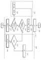
Translated fromKorean도 1은 본 발명에 따른 리페어가 가능한 멀티칩에 대한 실시예를 보여주고 있다.1 shows an embodiment of a repairable multichip according to the present invention.
도 2는 본 발명에 따른 메모리 칩의 메모리 코어를 보여주고 있다.2 shows a memory core of a memory chip according to the present invention.
도 3은 본 발명에 따른 멀티칩의 메모리 칩들에 대한 리페어 방법을 보여주는 실시예이다.3 is a diagram illustrating a repairing method for memory chips of a multichip according to the present invention.
도 4은 본 발명의 퓨즈박스의 또 다른 실시예를 보여주고 있다.Figure 4 shows another embodiment of the fuse box of the present invention.
도 5는 도 4에 도시된 메모리칩들로 이루어진 멀티칩에서 메모리칩들의 리페어 방법을 보여주고 있다.FIG. 5 illustrates a method of repairing memory chips in a multichip including the memory chips shown in FIG. 4.
*도면의 주요부분에 대한 부호의 설명** Description of the symbols for the main parts of the drawings *
휴대용 단말기: 1 테스터: 2Handheld Terminal: 1 Tester: 2
메모리칩: 100,200,300 테스트 콘트롤러: 20Memory chip: 100,200,300 Test controller: 20
메모리 셀: 122 리던던시 셀: 124Memory cells: 122 Redundancy cells: 124
메모리 코어: 120,220,320 퓨즈 박스: 140,240,340Memory Core: 120,220,320 Fuse Box: 140,240,340
퓨즈 제어 블럭: 160,260,360Fuse Control Blocks: 160,260,360
제 1 퓨즈 박스: 142 제 2 퓨즈 박스: 144First fuse box: 142 Second fuse box: 144
본 발명은 멀티칩에 관한 것으로, 좀 더 구체적으로 리페어가 가능한 멀티칩 및 그것의 리페어 방법에 관한 것이다.The present invention relates to a multichip, and more particularly, to a multichip capable of repair and a repair method thereof.
근래에 스마트 폰, PDA 혹은 네비게이션 응용제품들은 저전력 기능 구현을 위하여 SiP, MCP 혹은 POP 기술을 적용한 멀티칩들을 이용하고 있다. 이러한 멀티칩들은 단품 제어칩과 단품 메모리 등의 2개 이상의 칩들을 스택 공정을 통하여 쌓아 올린 것이다. 이때 각각의 단품 칩들은 양품으로 선별된 것들이다. 그러나 멀티칩은 스택 공정을 거치면서 각 칩들간의 인터페이스 상에서 일부 셀들이 타이밍, 로드 혹은 저항 등에 대하여 불량이 발생할 수 있다.Recently, smart phones, PDAs or navigation applications use multichips with SiP, MCP or POP technology to implement low power functions. These multi-chips are stacked two or more chips, such as a single control chip and a single memory through a stacking process. At this time, each one-piece chips are those selected as good. However, in the multi-chip stack process, some cells may fail in timing, load, or resistance on the interface between the chips.
종래의 멀티칩은 스택공정을 거친 후 발생한 불량에 대한 리페어 기능이 없다. 이는 메모리 가격, 로직 칩 가격, 스택 공정비용, 테스트 비용 등을 고려할 때 커다란 경제적 손실이 되고 있다.Conventional multichips do not have a repair function for defects that occur after the stacking process. This is a significant economic loss when considering memory prices, logic chip prices, stack process costs, and test costs.
본 발명은 상술한 문제점을 해결하기 위하여 제안된 것으로, 본 발명의 목적은 수율 향상 및 비용절감의 효과를 얻기 위하여 리페어 기능을 제공하는 멀티칩 및 그것의 리페어 방법을 제공하는데 있다.The present invention has been proposed to solve the above problems, and an object of the present invention is to provide a multi-chip and a repair method thereof that provides a repair function in order to obtain the effect of yield improvement and cost reduction.
본 발명에 따른 복수의 메모리 칩을 포함하고, 상기 복수의 메모리 칩은 단품 상태에서 리페어하고 남은 리던던시 셀에 대한 정보를 저장하고 있는 멀티칩의 리페어 방법은: (a) 상기 복수의 메모리 칩 중에서 어느 하나의 메모리 칩을 테스트하는 단계; (b) 상기 메모리 칩이 불량일 때, 상기 저장된 리던던시 셀의 정보에 의해 상기 메모리 칩이 리페어가 가능한지를 확인하는 단계; 및 (c) 상기 메모리 칩이 리페어 가능할 때, 상기 메모리 칩을 리페어하는 단계를 포함한다.A multi-chip repair method comprising a plurality of memory chips according to the present invention, wherein the plurality of memory chips store information on the redundancy cells remaining after repairing in a single unit state: (a) any of the plurality of memory chips Testing one memory chip; (b) when the memory chip is defective, checking whether the memory chip can be repaired based on the stored redundancy cell information; And (c) when the memory chip is repairable, repairing the memory chip.
실시예에 있어서, 상기 (b) 단계에서 상기 메모리 칩이 리페어가 불가능하다면, 상기 멀티칩을 불량 처리하는 단계를 포함한다.In an exemplary embodiment, if the memory chip cannot be repaired in the step (b), the method may include failing the multichip.
실시예에 있어서, 상기 멀티칩은 상기 (a) 단계에서 상기 메모리 칩이 불량이 아니라면, 상기 복수의 메모리 칩 중에서 다음 메모리 칩에 대하여 상기 (a) 내지 상기 (c) 단계를 반복하도록 제어하는 테스트 콘트롤러를 포함한다.In an embodiment, the multi-chip is a test for controlling the steps (a) to (c) to be repeated for the next memory chip among the plurality of memory chips if the memory chip is not defective in the step (a). Contains a controller.
실시예에 있어서, 상기 복수의 메모리 칩이 모두 불량이 아니라면, 상기 멀티칩을 양품 처리하는 단계를 포함한다.In an embodiment, if the plurality of memory chips are not all defective, a step of good quality processing of the multichip is included.
실시예에 있어서, 상기 테스트 콘트롤러는 상기 (c) 단계 이후, 상기 메모리 칩을 다시 상기(a) 내지 상기 (c) 단계를 반복하도록 한다.In an embodiment, the test controller causes the memory chip to repeat steps (a) to (c) after step (c).
실시예에 있어서, 상기 복수의 메모리 칩은, 리페어 신호에 응답하여 불량 메모리 셀의 어드레스를 상기 리던던시 셀의 어드레스로 치환하는 리던던시 회로; 및 상기 리던던시 셀의 정보를 저장하고, 상기 리던던시 회로를 제어하는 상기 리페어 신호를 생성하는 리던던시 제어회로를 포함한다.The memory chip may include: a redundancy circuit configured to replace an address of a bad memory cell with an address of the redundancy cell in response to a repair signal; And a redundancy control circuit that stores information of the redundancy cell and generates the repair signal for controlling the redundancy circuit.
실시예에 있어서, 상기 리던던시 회로는 퓨즈들을 포함하되, 상기 퓨즈들을 커팅하여 상기 불량 메모리 셀의 어드레스를 상기 리던던시 셀의 어드레스로 치환한다.In an embodiment, the redundancy circuit includes fuses, and the fuses are cut to replace the address of the bad memory cell with the address of the redundancy cell.
실시예에 있어서, 상기 퓨즈들을 커팅하기 위하여 이퓨즈(EFUSE) 방식을 이용한다.In an embodiment, an EFUSE method is used to cut the fuses.
실시예에 있어서, 상기 리던던시 제어회로는 상기 메모리 칩을 단품 상태에서 리페어하고 남은 리던던시 셀의 개수에 대한 정보를 저장하고 있으며, 상기 남은 리던던시 셀의 개수에 따라 상기 메모리 칩의 리페어 가능 여부를 결정한다.The redundancy control circuit may store information on the number of remaining redundancy cells after repairing the memory chip in a single product state, and determines whether to repair the memory chip according to the number of remaining redundancy cells. .
실시예에 있어서, 상기 멀티칩은 상기 (a) 단계에서 상기 메모리 칩이 불량이 아니라면, 상기 복수의 메모리 칩 중에서 다음 메모리 칩에 대하여 상기 (a) 내지 상기 (c) 단계를 반복하도록 제어하는 단계를 포함하되, 상기 제어는 외부의 테스트 장비가 한다.In an embodiment, the multi-chip controls to repeat steps (a) to (c) with respect to a next memory chip among the plurality of memory chips if the memory chip is not defective in the step (a). Including, but the control is made by external test equipment.
실시예에 있어서, 상기 복수의 메모리 칩이 모두 불량이 아니라면, 상기 멀티칩을 양품 처리하는 단계를 포함한다.In an embodiment, if the plurality of memory chips are not all defective, a step of good quality processing of the multichip is included.
실시예에 있어서, 상기 외부의 테스트 장비는 상기 (c) 단계 이후, 상기 메모리 칩을 다시 상기(a) 내지 상기 (c) 단계를 반복하도록 한다.In an embodiment, the external test equipment causes the memory chip to repeat steps (a) through (c) after step (c).
실시예에 있어서, 상기 복수의 메모리 칩은, 리페어 신호에 응답하여 불량 메모리 셀의 어드레스를 상기 리던던시 셀의 어드레스로 치환하는 리던던시 회로; 및 상기 리던던시 셀의 정보를 저장하고, 상기 리던던시 회로를 제어하는 상기 리페어 신호를 생성하는 리던던시 제어회로를 포함한다.The memory chip may include: a redundancy circuit configured to replace an address of a bad memory cell with an address of the redundancy cell in response to a repair signal; And a redundancy control circuit that stores information of the redundancy cell and generates the repair signal for controlling the redundancy circuit.
실시예에 있어서, 상기 리던던시 회로는 퓨즈들을 포함하되, 상기 퓨즈들을 커팅하여 상기 불량 메모리 셀의 어드레스를 상기 리던던시 셀의 어드레스로 치환한다.In an embodiment, the redundancy circuit includes fuses, and the fuses are cut to replace the address of the bad memory cell with the address of the redundancy cell.
실시예에 있어서, 상기 퓨즈들을 커팅하기 위하여 이퓨즈(EFUSE) 방식을 이용하는 멀티칩의 리페어 방법.The repair method of a multi-chip according to an embodiment, which uses an EFUSE method to cut the fuses.
실시예에 있어서, 상기 리던던시 제어회로는 상기 메모리 칩을 단품 상태에서 리페어하고 남은 리던던시 셀의 개수에 대한 정보를 저장하고 있으며, 상기 남은 리던던시 셀의 개수에 따라 상기 메모리 칩의 리페어 가능 여부를 결정한다.The redundancy control circuit may store information on the number of remaining redundancy cells after repairing the memory chip in a single product state, and determines whether to repair the memory chip according to the number of remaining redundancy cells. .
실시예에 있어서, 상기 복수의 메모리 칩은, 리페어 신호에 응답하여 불량 메모리 셀의 어드레스를 상기 리던던시 셀의 어드레스로 치환하는 리던던시 회로; 및 상기 리던던시 회로를 제어하는 상기 리페어 신호를 생성하는 리던던시 제어회로를 포함하되, 상기 리던던시 회로는 제 1 리페어 신호에 응답하여 단품 상태의 상기 메모리 칩을 리페어 하는데 이용되는 제 1 퓨즈 박스; 및 제 2 리페어 신호에 응답하여 멀티칩 상태의 메모리 칩을 리페어 하는데 이용되는 제 2 퓨즈 박스를 포함한다.The memory chip may include: a redundancy circuit configured to replace an address of a bad memory cell with an address of the redundancy cell in response to a repair signal; And a redundancy control circuit for generating the repair signal for controlling the redundancy circuit, wherein the redundancy circuit comprises: a first fuse box used to repair the memory chip in a unitary state in response to a first repair signal; And a second fuse box used to repair the memory chip in the multichip state in response to the second repair signal.
실시예에 있어서, 상기 리던던시 제어회로는 상기 외부의 테스트 장비에서 제공된 리페어 명령에 따라 상기 메모리 칩의 리페어가 단품 상태의 리페어인지 혹은 멀티칩 상태의 리페어인지를 확인하고, 상기 제 1 리페어 신호를 생성하여 상기 제 1 퓨즈 박스에 전달하거나 혹은 상기 제 2 리페어 신호를 생성하여 상기 제 2 퓨즈 박스에 전달한다.The redundancy control circuit may determine whether the repair of the memory chip is a single unit repair or a multichip repair unit according to a repair command provided from the external test equipment, and generate the first repair signal. The first fuse box may be transferred to the first fuse box, or the second repair signal may be generated and transferred to the second fuse box.
본 발명에 따른 또 다른 복수의 메모리 칩을 포함하는 멀티칩의 리페어 방법은: (a) 상기 복수의 메모리 칩 중에서 어느 하나의 메모리 칩을 테스트하는 단계; 및 (b) 상기 메모리 칩이 불량일 때 상기 메모리 칩을 리페어하는 단계를 포함하는 단계를 포함하고, 상기 각각의 메모리 칩은, 리페어 신호에 응답하여 불량 메모리 셀의 어드레스를 상기 리던던시 셀의 어드레스로 치환하는 리던던시 회로; 및 상기 리던던시 회로를 제어하는 상기 리페어 신호를 생성하는 리던던시 제어회로를 포함하되, 상기 리던던시 회로는 제 1 리페어 신호에 응답하여 단품 상태의 상기 메모리 칩을 리페어 하는데 이용되는 제 1 퓨즈 박스; 및 제 2 리페어 신호에 응답하여 멀티칩 상태의 메모리 칩을 리페어 하는데 이용되는 제 2 퓨즈 박스를 포함한다.According to another aspect of the present invention, there is provided a repair method of a multichip including a plurality of memory chips, the method including: (a) testing one of the plurality of memory chips; And (b) repairing the memory chip when the memory chip is defective, wherein each memory chip is configured to replace an address of the defective memory cell with an address of the redundancy cell in response to a repair signal. Replacing redundancy circuit; And a redundancy control circuit for generating the repair signal for controlling the redundancy circuit, wherein the redundancy circuit comprises: a first fuse box used to repair the memory chip in a unitary state in response to a first repair signal; And a second fuse box used to repair the memory chip in the multichip state in response to the second repair signal.
실시예에 있어서, 상기 리던던시 제어회로는 상기 테스트 콘트롤러에서 제공된 리페어 명령에 따라 상기 메모리 칩의 리페어가 단품 상태의 리페어인지 혹은 멀티칩 상태의 리페어인지를 확인하고, 상기 제 1 리페어 신호를 생성하여 상기 제 1 퓨즈 박스에 전달하거나 혹은 상기 제 2 리페어 신호를 생성하여 상기 제 2 퓨즈 박스에 전달한다.The redundancy control circuit may determine whether the repair of the memory chip is a single unit repair or a multichip repair unit according to a repair command provided from the test controller, and generates the first repair signal to generate the first repair signal. The first fuse box may be transferred or the second repair signal may be generated and transferred to the second fuse box.
본 발명에 따른 멀티칩은: 복수의 메모리 칩; 및 상기 복수의 메모리칩을 패키지 레벨에서 테스트할 때 상기 복수의 메모리 칩을 제어하는 테스트 콘트롤러를 포함하되, 각각의 메모리 칩은, 복수의 메모리 셀 및 복수의 리던던시 셀을 가지는 메모리 코어; 리페어 신호에 응답하여 상기 복수의 메모리 셀 중에서 불량이 발생한 메모리 셀을 상기 복수의 리던던시 셀로 치환하기 위한 리던던시 회로; 및 단품 상태에서 리페어하는데 사용된 상기 리던던시 셀의 개수를 저장하며, 리페어 명령에 응답하여 상기 리페어 신호를 생성하는 리던던시 제어 회로를 포함하되, 상기 테스트 콘트롤러는 상기 리던던시 제어 회로에 저장된 상기 리던던시 셀의 개수를 파악하여 상기 리페어 명령을 생성하여 상기 리던던시 제어회로에 전달한다.The multichip according to the present invention comprises: a plurality of memory chips; And a test controller that controls the plurality of memory chips when testing the plurality of memory chips at a package level, each memory chip having a plurality of memory cells and a plurality of redundancy cells; A redundancy circuit for replacing a defective memory cell among the plurality of memory cells with the plurality of redundancy cells in response to a repair signal; And a redundancy control circuit configured to store the number of the redundancy cells used for repairing in a single unit state, and to generate the repair signal in response to a repair command, wherein the test controller includes the number of the redundancy cells stored in the redundancy control circuit. Identify and generate the repair command and transmit it to the redundancy control circuit.
실시예에 있어서, 상기 리던던시 회로는 퓨즈 컷팅을 통하여 상기 복수의 메모리 셀 중에서 불량 메모리 셀의 어드레스를 상기 리던던시 메모리 셀의 어드레스로 치환한다.In an embodiment, the redundancy circuit replaces an address of a bad memory cell among the plurality of memory cells with an address of the redundancy memory cell through fuse cutting.
실시예에 있어서, 상기 퓨즈 컷팅은 이퓨즈(EFUSE) 방식을 이용한다.In an embodiment, the fuse cutting uses an EFUSE method.
본 발명에 따른 멀티칩은: 복수의 메모리 칩을 포함하되, 각각의 메모리 칩은, 복수의 메모리 셀 및 복수의 리던던시 셀을 가지는 메모리 코어; 제 1 리페어 신호에 응답하여 단품 상태의 상기 메모리 칩의 불량 메모리 셀을 상기 리던던시 셀로 치환하는 제 1 퓨즈 박스; 제 2 리페어 신호에 응답하여 멀티칩 상태의 상기 메모리 칩의 불량 메모리 셀을 상기 리던던시 셀로 치환하는 제 2 퓨즈 박스; 및 단품 상태에서 상기 메모리 칩을 리페어할 때 상기 제 1 리페어 신호를 생성하여 상기 제 1 퓨즈 박스에 전달하고, 멀티칩 패키지 상태에서 상기 메모리 칩을 리페어할 때 상기 제 2 리페어 신호를 생성하여 상기 제 2 퓨즈 박스에 전달하는 퓨즈박스 제어회로를 포함한다.A multichip according to the present invention comprises: a memory core comprising a plurality of memory chips, each memory chip having a plurality of memory cells and a plurality of redundancy cells; A first fuse box for replacing a defective memory cell of the memory chip in a single state with the redundancy cell in response to a first repair signal; A second fuse box for replacing a defective memory cell of the memory chip in a multichip state with the redundancy cell in response to a second repair signal; And generating the first repair signal and transmitting the first repair signal to the first fuse box when the memory chip is repaired in a single product state, and generating the second repair signal when repairing the memory chip in a multichip package state. 2 includes a fuse box control circuit for transmitting to the fuse box.
본 발명에 따른 또 다른 멀티칩은: 복수의 메모리 칩을 포함하고, 각각의 메모리 칩은, 복수의 메모리 셀 및 복수의 리던던시 셀을 가지는 메모리 코어; 리페어 신호에 응답하여 단품 상태의 상기 메모리 칩의 불량 메모리 셀을 상기 리던던시 셀로 치환하는 퓨즈 박스; 단품 상태에서 상기 메모리 칩을 리페어할 때 사용된 리던던시 셀의 개수를 저장해 두고, 멀티칩 패키지 상태에서 상기 메모리 칩을 리페어할 때 상기 저장된 리던던시 셀의 개수로 상기 메모리 칩의 리페어 가능 여부를 확인하여 상기 리페어 신호를 생성하여 상기 퓨즈 박스에 전달하는 퓨즈박스 제어회로를 포함한다.Another multichip according to the present invention comprises: a memory core having a plurality of memory chips, each memory chip having a plurality of memory cells and a plurality of redundancy cells; A fuse box for replacing a defective memory cell of the memory chip in a single state with the redundancy cell in response to a repair signal; The number of redundancy cells used when the memory chip is repaired in a single unit state is stored, and when the memory chip is repaired in a multi-chip package state, the memory chips are checked whether the memory chip can be repaired based on the number of the redundant cells. And a fuse box control circuit configured to generate a repair signal and transmit the repair signal to the fuse box.
이하, 본 발명이 속하는 기술분야에서 통상의 지식을 가진 자가 본 발명의 기술적 사상을 용이하게 실시할 수 있도록 본 발명의 실시예를 첨부된 도면을 참조하여 설명한다.DETAILED DESCRIPTION Hereinafter, exemplary embodiments of the present invention will be described with reference to the accompanying drawings so that those skilled in the art may easily implement the technical idea of the present invention.
도 1은 본 발명에 따른 리페어가 가능한 멀티칩(1)에 대한 실시예를 보여주고 있다. 도 1을 참조하면, 멀티칩(1)은 테스트 콘트롤러(10) 및 메모리 칩들(20)을 포함하고 있다.1 shows an embodiment of a
테스트 콘트롤러(10)는 테스터(2)로부터 테스트 신호를 전달받아 각각의 메모리칩들(20)의 테스트를 제어한다. 테스트 콘트롤러(10)는 테스터(2)가 멀티칩(1)의 메모리 칩들(20)을 차례로 테스트하도록 제어한다. 테스트 콘트롤러(10)는 또한 각각의 메모리 칩들(20)을 테스트하고, 리페어 가능 여부를 확인한 후, 불량 메모리 칩에 대한 리페어도 제어한다. 테스트 콘트롤러(10)는 각각의 메모리 칩들(100,200,300)을 차례로 테스트하고 리페어를 실시한 후, 모든 메모리 칩들(100,200,300)에 대하여 불량이 없다고 확인되면, 멀티칩(1)의 양품임을 나타내는 신호를 생성하여 테스터(2)에 전달한다.The
메모리 칩들(20)은 복수의 메모리 칩(100,200,300)을 스택 구조로 쌓아 놓은 구조이다. 메모리 칩들(20)은 메모리 코어들(120,220,320), 퓨즈 박스들(140,240,340) 및 퓨즈 제어 로직들(160,260,360)을 각각 포함하고 있다. 여기서 각각의 메모리 칩들(100,200,300)은 단품 테스트에서 양품으로 판정을 받은 것들이다. 그러나 이러한 메모리 칩들(100,200,300)이 단품 테스트에서 양품이라고 판정을 받았지만, 스택 공정을 거치면서 불량이 날 수 있다.The
메모리 코어들(120,220,320)은 복수의 메모리 셀과 복수의 리던던시 셀을 포함하고 있다. 도 2는 본 발명의 메모리 칩(100)의 메모리 코어(120)을 보여주고 있다. 도 2를 참조하면, 메모리 코어(1200)는 복수의 메모리 셀(122) 및 복수의 리던던시 셀(124)을 포함하고 있다.The
퓨즈 박스들(140,240,340)은 불량 판정을 받은 메모리 셀의 어드레스를 리던던시 셀의 어드레스로 치환해 주는 퓨즈 컷팅 프로그래밍에 사용된다. 이러한 퓨즈 컷팅 프로그래밍 방식에는 과전류로 퓨즈를 녹여 끊어버리는 전기 퓨즈 방식, 레이저 빔으로 퓨즈를 태워 버리는 방식, 레이저 빔으로 접합부를 단락시키는 방식, EPPROM 메모리셀로 프로그램하는 방식 등이 있다.The
퓨즈 제어 로직들(160,260,360)은 불량 메모리 셀의 어드레스를 리던던시의 셀의 어드레스로 치환하기 위한 리페어 신호(RS)를 생성하여 퓨즈 박스들(140,240,340)에 전달한다. 퓨즈 박스들(140,240,340)은 리페어 신호(RS)에 응답하여 퓨즈를 컷팅하여 불량 메모리 셀의 어드레스는 리던던시 셀의 어드레스로 치환시킨다. The
멀티칩(1)의 메모리 칩들(100,200,300)을 테스트하고 불량셀을 발견할 경우, 퓨즈 제어 로직들(160,260,360)은 메모리 칩들(100,200,300)의 리페어가 가능한지 확인한 후 리페어 신호(RS)을 퓨즈 박스들(140,240,340)에 전달한다.When the
퓨즈 제어 로직들(160,260,360)은 단품 테스트를 거친 메모리 칩들(100,200,300)에 남아있는 리던던시 개수를 파악하기 위한 카운터(도시되어 있지 않음)을 포함하고 있다. 카운터는 메모리 단품 테스트 후 리페어하면서 사용된 리던던시 셀의 개수를 카운트하여 저장하고 있다. 퓨즈 제어 로직들(160,260,360)은 카운터에 저장된 사용된 리던던시 셀의 개수를 파악하여, 멀티칩(1)의 메모리 칩들(100,200,300)의 불량 메모리 셀의 리페어 가능 여부를 결정하게 된다. 퓨즈 제어 로직들(160,260,360)은 메모리 칩들(100,200,300)의 리페어가 가능하지 않다고 판단되면, 해당 메모리 칩을 불량처리 하는 신호를 생성하여 테스트 콘트롤러(20) 전달한다.The
본 발명의 멀티칩(1)은 퓨즈 제어 로직들(160,260,360)을 구비하고 있어, 멀티칩(1)의 메모리 칩들(100,200,300)을 테스트하여 리페어를 할 수 있게 한다.The
도 3은 본 발명에 따른 멀티칩(1)의 메모리 칩들(100,200,300)에 대한 리페어 방법을 보여주는 실시예이다.3 is a diagram illustrating a repair method for
S100 단계에서는 멀티칩(1)이 불량처리되는 과정을 보여주고 있다. S200단계에서는 멀티칩(1)의 메모리 칩들(100,200,300)을 리페어하는 과정을 보여주고 있다. S300 단계에서는 멀티칩(1)이 양품처리되는 과정을 보여주고 있다.In step S100, the
S100 단계의 불량처리되는 과정은 다음과 같이 진행된다.The process of the defective process of step S100 proceeds as follows.
S110 단계에서는 멀티칩(1)의 메모리 칩들(20)중에서 테스트하게 될 칩을 선택하게 된다. 테스트 콘트롤러(20)는 테스터(2)로부터 전달된 테스트 신호에 응답하여 메모리 칩들(20)을 테스트한다. 여기서는 설명의 편의를 위하여, i=0일 때, 메모리 칩(100)을 테스트하고, i=1일 때 메모리 칩(200)을 테스트한다고 가정하겠다.In step S110, the chip to be tested is selected from among the
S120 단계에서는 선택된 메모리 칩(100)에 대하여 테스트를 실시하게 된다. 여기서 테스트는 자체적으로 리페어 기능을 가진 테스트이다. 테스트는 BIRA(Built In Self Repair) 테스트일 수 있다. BIRA 테스트는 로우, 칼럼 리던던시를 가진 메모리 칩에 대해 테스트 및 리던던시 분석을 수행하고 결함이 있는 메모리 칩에 대해 리페어 정보를 출력하고 퓨즈 컷팅을 통한 리페어를 할 수 있다.In operation S120, a test is performed on the selected
S130 단계에서는 테스트된 메모리 칩(100)이 불량인가를 확인한다.In step S130 it is checked whether the tested
S140 단계에서는 메모리 칩(100)에 불량 메모리 셀이 있을 때, 메모리 칩(100)의 리페어가 가능한지를 확인한다. 퓨즈 제어 로직(160)은 단품 테스트에서 사용된 리던던시 셀의 개수를 이용하여 남아있는 리던던시 셀을 파악하고, 불량 메모리 셀의 개수와 비교하여 리페어가 가능여부를 확인한다. 리페어가 가능한다면, 퓨즈 제어 로직(160)은 리페어 신호(RS)를 생성하여, 퓨즈 블럭(140)에 전달한다. 리페어가 가능하지 않다면, 퓨즈 제어 로직(160)은 메모리 칩(100)이 불량임을 나타내는 신호를 생성하여 테스트 콘트롤러(20)에 전달한다.In step S140, when there is a bad memory cell in the
S150 단계에서는 테스트 콘트롤러(20)에 전달된 메모리 칩(100)에 대한 불량임을 나타내는 신호를 전달받아 멀티칩(1)이 불량임을 결정한다.In operation S150, the
S200 단계의 리페어되는 과정은 다음과 같다. S210 단계에서는 리페어가 가능한 반도체 칩(100)을 리페어하게 된다. 퓨즈 박스(140)는 S140단계에서 퓨즈 제어 로직(160)으로부터 전달된 리페어 신호(RS)에 응답하여, 해당 불량 메모리 셀의 어드레스를 리던던시 셀의 어드레스로 치환하도록 퓨즈 컷팅을 실시한다. 따라서 불량 셀을 포함하고 있던 메모리 칩(100)을 리페어하게 된다. 리페어된 메모리 칩(100)은 리페어가 제대로 되었는지 확인하기 위하여 테스트를 실시하기 위해 S120단계로 되돌아간다.Repair process of step S200 is as follows. In operation S210, the
S300 단계의 양품처리 과정은 다음과 같다.Good quality treatment process of step S300 is as follows.
S310 단계에서는 메모리 칩(100)이 불량이 없을 때, 모든 메모리 칩들(100,200,300)이 불량이 없는가를 판단한다. 메모리 칩(100)은 모든 메모리 칩이 아니기 때문에 다음 메모리 칩(200)을 테스트해야 한다.In operation S310, when the
S320 단계에서는 i를 하나 추가하여, 다음 메모리 칩(200)이 테스트를 실시하게 한다. 테스트 콘트롤러(20)는 메모리 칩(100)이 불량이 없는 것을 확인한 후, 다음 메모리 칩(200)을 테스트하기 위하여 제어 신호를 메모리 칩(200)에 전달한다. 테스트 콘트롤러(20)는 메모리 칩(200)에 대하여 메모리 칩(100)을 테스트하고 리페어 하였던 동일한 과정을 실시하게 된다.In operation S320, one i is added to allow the
S330 단계에서는 멀티칩(1)의 모든 메모리 칩들(100,200,300)들이 불량이 없음이 확인되면, 멀티칩(1)을 양품처리한다.In step S330, when all the
도 4는 본 발명의 퓨즈박스(140) 및 퓨즈 제어 블럭(160)의 또 다른 실시예를 보여주고 있다.4 shows another embodiment of the
도 4를 참조하면, 퓨즈 박스(140)는 제 1 퓨즈 박스(142)와 제 2 퓨즈 박스(144)를 포함하고 있다. 제 1 퓨즈 박스(142)는 단품 상태에서 메모리 칩(100)을 테스트하고 리페어하는데 사용되는 퓨즈들을 포함하고 있다. 제 2 퓨즈 박스(144)는 멀티칩 상태에서 메모리 칩(100)을 테스트하고 리페어하는데 사용되는 퓨즈들을 포함하고 있다.Referring to FIG. 4, the
퓨즈 제어 블럭(160)은 단품 테스트일 때, 리페어 신호(SRS)를 생성하여 제 1 퓨즈 박스(142)에 전달한다. 한편, 멀티칩 상태에서 메모리 칩(100)을 테스트를 할 때, 퓨즈 제어 블럭(160)은 테스트 콘트롤러(20)로부터 테스트 신호를 전달받아 리페어 신호(MRS)를 생성하여 제 2 퓨즈 박스(144)에 전달한다.When the
도 4에서 메모리칩(100)의 구성에 대하여 설명하였다. 한편 멀티칩(1)의 내의 다른 메모리칩들(200,300)도 도 4의 메모리칩(100)과 동일한 구성을 가지고 있다.In FIG. 4, the configuration of the
도 5는 도 4에 도시된 메모리칩들로 이루어진 멀티칩(1)에서 메모리칩들(100,200,300)의 리페어 방법을 보여주고 있다. 도 5를 참조하면, 메모칩들(100,200,300)의 리페어 방법은 S400의 불량처리 과정과 S500의 양품처리 과정을 포함하고 있다.FIG. 5 illustrates a repair method of the
S400의 불량처리 과정은 다음과 같다.The failure process of S400 is as follows.
S410 단계에서는 테스터(2)의 테스트 신호에 응답하여, 테스트 콘트롤러(20)는 메모리칩들(100,200,300)중 메모리칩(100)을 선택한다.In operation S410, in response to the test signal of the
S420 단계에서는 S410 단계에서 선택된 메모리칩(100)에 대한 테스트를 실시한다. 테스트 콘트롤러(20)는 테스트 신호에 응답하여, 메모리칩(100)을에 대한 테스트를 실시한다.In operation S420, a test is performed on the
S430 단계에서는 메모리칩(100)이 불량인가를 확인한다. 테스트 콘트롤러(20)는 S420 단계에서 테스트한 메모리칩(100)에 불량셀이 있는가를 체크한다. 불량셀이 있다면, 리페어 명령을 생성하여 퓨즈 제어 블럭(160)에 전달한다.In operation S430, it is checked whether the
S440 단계에서는 불량셀이 존재하는 메모리칩(100)에 대한 리페어를 실시한다. 퓨즈 제어 블럭(160)는 테스트 콘트롤러(20)로부터 전달된 리페어 명령을 입력받아, 리페어 신호(MRS)를 생성하여 퓨즈 박스(140)내의 제 2 퓨즈 박스(144)에 전달한다. 여기서 제 2 퓨즈 박스(144)는 멀티칩용 퓨즈 박스이다. 제 2 퓨즈 박스(144)는 리페어 신호(MRS)에 응답하여, 불량 메모리 셀의 어드레스를 리던던시 메모리 셀 어드레스로 치환하도록 퓨즈 컷팅이 실시된다.In operation S440, a repair of the
S450 단계에서는 S440단계에서 리페어된 메모리칩(100)에 대한 테스트를 재실시하여 불량인가를 확인한다.In operation S450, the test on the
S460 단계에서는 메모리칩(100)의 불량이 리페어가 가능한가를 확인한다. 테스트 콘트롤러(20)는 리페어된 메모리칩(100)의 불량을 확인하면, 테스트 신호를 퓨즈 제어 블럭(160)에 전달한다. 퓨즈 제어 블럭(160)은 테스트 신호에 응답하여, 리던던시 셀의 개수와 불량셀의 개수를 비교하여 리페어가 가능한지를 결정한다. 리페어가 가능하면, 퓨즈 제어 블럭(160)는 리페어 신호(MRS)를 퓨즈박스(140)의 제 2 퓨즈박스(144)에 전달하여 S440 단계를 다시 실시한다. 리페어가 불가능하면, 퓨즈 제어 블럭(160)은 메모리칩(100)의 불량을 결정하는 신호를 생성하여 테스트 콘트롤러(20)에 전달한다.In operation S460, whether the defect of the
S470 단계에서는 리페어가 불가능한 메모리칩(100)에 대한 불량처리를 결정한다. 테스트 콘트롤러(20)는 퓨즈 제어 블럭(160)으로부터 전달된 불량신호에 응답하여 멀티칩(1)의 불량을 결정하는 신호를 생성하여 테스터(2)에 전달한다.In operation S470, the defect processing on the
S500 단계의 양품처리 과정은 다음과 같다.Good quality processing of step S500 is as follows.
S510 단계에서는 불량이 아닌 메모리칩들(100,200,300)들이 모든 메모리칩인가를 판단한다. 테스트 콘트롤러(20)는 S430 단계와 S460 단계의 메모리칩(100)이 모든 메모리칩인가를 확인한다. 모든 메모리칩이 아니라면, 다음 메모리칩(200)을 테스트하기 위하여, 메모리칩(200)에 테스트 신호를 전달한다.In operation S510, it is determined whether the
S520 단계에서는 테스트 콘트롤러(20)가 다음 메모리칩(200)을 테스트하기 위하여 i를 하나 증가시켜 S420 단계의 메모리칩(200)을 테스트하게 된다.In step S520, the
S530 단계에서는 모든 메모리칩이라면, 테스트 콘트롤러(20)는 멀티칩(1)이 양품임을 결정하는 신호를 생성하여 테스터(2)에 전달한다.In step S530, if all of the memory chips, the
한편, 본 발명의 상세한 설명에서는 구체적인 실시예에 관하여 설명하였으나, 본 발명의 범위에서 벗어나지 않는 한도 내에서 여러 가지로 변형할 수 있다. 그러므로 본 발명의 범위는 상술한 실시예에 국한되어 정해져서는 안되며 후술하는 특허청구범위 뿐만 아니라 이 발명의 특허청구범위와 균등한 것들에 의해 정해져야 한다.Meanwhile, in the detailed description of the present invention, specific embodiments have been described, but various modifications may be made without departing from the scope of the present invention. Therefore, the scope of the present invention should not be limited to the above-described embodiments, but should be defined by the equivalents of the claims of the present invention as well as the following claims.
상술한 바와 같이 본 발명에 따른 멀티칩은 메모리칩에 퓨즈 박스와 그것을 제어하는 퓨즈 제어 블럭을 구비하여, 멀티칩 상태에서 메모리칩을 리페어를 할 수 있게 된다.As described above, the multichip according to the present invention includes a fuse box and a fuse control block for controlling the same in the memory chip, so that the memory chip can be repaired in the multichip state.
Claims (25)
Translated fromKoreanPriority Applications (2)
| Application Number | Priority Date | Filing Date | Title |
|---|---|---|---|
| KR1020060097304AKR100897285B1 (en) | 2006-10-02 | 2006-10-02 | Multichip and its repair method |
| US11/904,187US7706198B2 (en) | 2006-10-02 | 2007-09-26 | Multi-chip and repairing method based on remaining redundancy cells |
Applications Claiming Priority (1)
| Application Number | Priority Date | Filing Date | Title |
|---|---|---|---|
| KR1020060097304AKR100897285B1 (en) | 2006-10-02 | 2006-10-02 | Multichip and its repair method |
Related Child Applications (1)
| Application Number | Title | Priority Date | Filing Date |
|---|---|---|---|
| KR1020080034171ADivisionKR20080045097A (en) | 2008-04-14 | 2008-04-14 | Multi chip and its repair method |
Publications (2)
| Publication Number | Publication Date |
|---|---|
| KR20080031078A KR20080031078A (en) | 2008-04-08 |
| KR100897285B1true KR100897285B1 (en) | 2009-05-14 |
Family
ID=39260993
Family Applications (1)
| Application Number | Title | Priority Date | Filing Date |
|---|---|---|---|
| KR1020060097304AExpired - Fee RelatedKR100897285B1 (en) | 2006-10-02 | 2006-10-02 | Multichip and its repair method |
Country Status (2)
| Country | Link |
|---|---|
| US (1) | US7706198B2 (en) |
| KR (1) | KR100897285B1 (en) |
Families Citing this family (10)
| Publication number | Priority date | Publication date | Assignee | Title |
|---|---|---|---|---|
| US8839053B2 (en)* | 2010-05-27 | 2014-09-16 | Microsoft Corporation | Error correcting pointers for non-volatile storage |
| US20250181491A1 (en)* | 2011-04-06 | 2025-06-05 | Smith Memory Technologies, LLC | System, method, and computer program product for improving memory systems |
| US9032244B2 (en) | 2012-11-16 | 2015-05-12 | Microsoft Technology Licensing, Llc | Memory segment remapping to address fragmentation |
| KR20150006167A (en)* | 2013-07-08 | 2015-01-16 | 에스케이하이닉스 주식회사 | Semiconductor system and repair memthod of the same |
| KR20160121230A (en)* | 2015-04-10 | 2016-10-19 | 에스케이하이닉스 주식회사 | Semiconductor Memory Apparatus, Repair System therefor, and Method for Managing of Apparatus Quality |
| CN111415700B (en)* | 2020-04-24 | 2022-05-06 | 西安紫光国芯半导体有限公司 | Repair method, repair device and computer storage medium |
| EP3992972B1 (en) | 2020-09-01 | 2024-09-04 | Changxin Memory Technologies, Inc. | Method and apparatus for determining failed bit repair scheme, and chip |
| CN114121129B (en)* | 2020-09-01 | 2023-09-12 | 长鑫存储技术有限公司 | Determination method, device and chip of failed bit repair plan |
| KR102408165B1 (en)* | 2021-10-01 | 2022-06-13 | (주)케이테크놀로지 | Repair analysis apparatus of tester for semiconductor device, method for repair analysis and tester for semiconductor device |
| KR20240122176A (en) | 2023-02-03 | 2024-08-12 | 삼성전자주식회사 | Memory repair circuit, memory repair method, and memory device |
Citations (5)
| Publication number | Priority date | Publication date | Assignee | Title |
|---|---|---|---|---|
| KR950011968B1 (en)* | 1990-09-20 | 1995-10-12 | 가부시끼가이샤 도시바 | Redundant Circuit Section Memory IC Test Device |
| KR0181204B1 (en)* | 1995-08-31 | 1999-04-15 | 김광호 | Self Repair Circuit of Semiconductor Memory Device |
| KR20010067326A (en)* | 1999-12-17 | 2001-07-12 | 아끼구사 나오유끼 | Self-test circuit and memory device incorporating it |
| KR20020038298A (en)* | 2000-11-17 | 2002-05-23 | 양우드워드 | Semiconductor device having embedded auto test and repair function and Method thereof |
| KR20030057299A (en)* | 2001-12-28 | 2003-07-04 | 삼성전자주식회사 | Semiconductor memory device post-repair circuit and Method |
Family Cites Families (7)
| Publication number | Priority date | Publication date | Assignee | Title |
|---|---|---|---|---|
| US5502333A (en)* | 1994-03-30 | 1996-03-26 | International Business Machines Corporation | Semiconductor stack structures and fabrication/sparing methods utilizing programmable spare circuit |
| US6141768A (en)* | 1998-03-12 | 2000-10-31 | Winbond Electronics Corp. | Self-corrective memory system and method |
| US6795942B1 (en)* | 2000-07-06 | 2004-09-21 | Lsi Logic Corporation | Built-in redundancy analysis for memories with row and column repair |
| US7237154B1 (en)* | 2001-06-29 | 2007-06-26 | Virage Logic Corporation | Apparatus and method to generate a repair signature |
| JP3644913B2 (en)* | 2001-07-23 | 2005-05-11 | 松下電器産業株式会社 | Semiconductor device |
| KR100443508B1 (en) | 2001-12-21 | 2004-08-09 | 주식회사 하이닉스반도체 | A semiconductor memory module |
| KR20040065776A (en) | 2003-01-16 | 2004-07-23 | 삼성전자주식회사 | Partial Rescue Multi-Chip Semiconductor Device and Method for partially rescuing thereof |
- 2006
- 2006-10-02KRKR1020060097304Apatent/KR100897285B1/ennot_activeExpired - Fee Related
- 2007
- 2007-09-26USUS11/904,187patent/US7706198B2/ennot_activeExpired - Fee Related
Patent Citations (5)
| Publication number | Priority date | Publication date | Assignee | Title |
|---|---|---|---|---|
| KR950011968B1 (en)* | 1990-09-20 | 1995-10-12 | 가부시끼가이샤 도시바 | Redundant Circuit Section Memory IC Test Device |
| KR0181204B1 (en)* | 1995-08-31 | 1999-04-15 | 김광호 | Self Repair Circuit of Semiconductor Memory Device |
| KR20010067326A (en)* | 1999-12-17 | 2001-07-12 | 아끼구사 나오유끼 | Self-test circuit and memory device incorporating it |
| KR20020038298A (en)* | 2000-11-17 | 2002-05-23 | 양우드워드 | Semiconductor device having embedded auto test and repair function and Method thereof |
| KR20030057299A (en)* | 2001-12-28 | 2003-07-04 | 삼성전자주식회사 | Semiconductor memory device post-repair circuit and Method |
Also Published As
| Publication number | Publication date |
|---|---|
| KR20080031078A (en) | 2008-04-08 |
| US7706198B2 (en) | 2010-04-27 |
| US20080080275A1 (en) | 2008-04-03 |
Similar Documents
| Publication | Publication Date | Title |
|---|---|---|
| KR100897285B1 (en) | Multichip and its repair method | |
| US6845477B2 (en) | Semiconductor test device for conducting an operation test in parallel on many chips in a wafer test and semiconductor test method | |
| US7512001B2 (en) | Semiconductor memory device, test system including the same and repair method of semiconductor memory device | |
| CN102237146B (en) | The reparation circuit of semiconductor storage and restorative procedure | |
| JPWO2007032184A1 (en) | Semiconductor device, semiconductor chip, interchip wiring test method, and interchip wiring switching method | |
| US6812557B2 (en) | Stacked type semiconductor device | |
| CN117198371A (en) | Three-dimensional chip, repairing method and electronic equipment | |
| KR101877939B1 (en) | Test circuit, memory system and test method of memory system | |
| CN103000226B (en) | The method of testing of defect is detected by RAM chip address pin | |
| US20080175079A1 (en) | Test scheme for fuse circuit | |
| JP4891748B2 (en) | Semiconductor integrated circuit and test method thereof | |
| US9019786B2 (en) | Repair system for repairing defect using E fuses and method of controlling the same | |
| KR20080045097A (en) | Multi chip and its repair method | |
| KR100944325B1 (en) | Repair fuse device | |
| US20120010731A1 (en) | System including semiconductor devices and controller and method for operating the same | |
| US6754865B2 (en) | Integrated circuit | |
| US20160042813A1 (en) | Semiconductor memory device and method for testing redundancy word line | |
| CN1327522C (en) | Semiconductor device with unloading circuit for removing defect part | |
| US20080010575A1 (en) | Semiconductor device | |
| JP5038788B2 (en) | Semiconductor device | |
| US7075836B2 (en) | Semiconductor memory having testable redundant memory cells | |
| CN1776820B (en) | Memory device capable of changing data output mode | |
| KR100630661B1 (en) | Memory device capable of high-speed operation test even with low frequency tester and its test method | |
| KR102033989B1 (en) | Semiconductor memory device and method of driving the same | |
| US20040030978A1 (en) | Semiconductor integrated circuit device having operation test function |
Legal Events
| Date | Code | Title | Description |
|---|---|---|---|
| A201 | Request for examination | ||
| PA0109 | Patent application | St.27 status event code:A-0-1-A10-A12-nap-PA0109 | |
| PA0201 | Request for examination | St.27 status event code:A-1-2-D10-D11-exm-PA0201 | |
| E902 | Notification of reason for refusal | ||
| PE0902 | Notice of grounds for rejection | St.27 status event code:A-1-2-D10-D21-exm-PE0902 | |
| AMND | Amendment | ||
| E13-X000 | Pre-grant limitation requested | St.27 status event code:A-2-3-E10-E13-lim-X000 | |
| P11-X000 | Amendment of application requested | St.27 status event code:A-2-2-P10-P11-nap-X000 | |
| P13-X000 | Application amended | St.27 status event code:A-2-2-P10-P13-nap-X000 | |
| E601 | Decision to refuse application | ||
| PE0601 | Decision on rejection of patent | St.27 status event code:N-2-6-B10-B15-exm-PE0601 | |
| PG1501 | Laying open of application | St.27 status event code:A-1-1-Q10-Q12-nap-PG1501 | |
| A107 | Divisional application of patent | ||
| AMND | Amendment | ||
| E13-X000 | Pre-grant limitation requested | St.27 status event code:A-2-3-E10-E13-lim-X000 | |
| J201 | Request for trial against refusal decision | ||
| P11-X000 | Amendment of application requested | St.27 status event code:A-2-2-P10-P11-nap-X000 | |
| P13-X000 | Application amended | St.27 status event code:A-2-2-P10-P13-nap-X000 | |
| PA0107 | Divisional application | St.27 status event code:A-0-1-A10-A18-div-PA0107 St.27 status event code:A-0-1-A10-A16-div-PA0107 | |
| PJ0201 | Trial against decision of rejection | St.27 status event code:A-3-3-V10-V11-apl-PJ0201 | |
| PB0901 | Examination by re-examination before a trial | St.27 status event code:A-6-3-E10-E12-rex-PB0901 | |
| E902 | Notification of reason for refusal | ||
| PE0902 | Notice of grounds for rejection | St.27 status event code:A-1-2-D10-D21-exm-PE0902 | |
| E13-X000 | Pre-grant limitation requested | St.27 status event code:A-2-3-E10-E13-lim-X000 | |
| P11-X000 | Amendment of application requested | St.27 status event code:A-2-2-P10-P11-nap-X000 | |
| P13-X000 | Application amended | St.27 status event code:A-2-2-P10-P13-nap-X000 | |
| B601 | Maintenance of original decision after re-examination before a trial | ||
| PB0601 | Maintenance of original decision after re-examination before a trial | St.27 status event code:N-3-6-B10-B17-rex-PB0601 | |
| J301 | Trial decision | Free format text:TRIAL DECISION FOR APPEAL AGAINST DECISION TO DECLINE REFUSAL REQUESTED 20080414 Effective date:20090130 | |
| PJ1301 | Trial decision | St.27 status event code:A-3-3-V10-V15-crt-PJ1301 Decision date:20090130 Appeal event data comment text:Appeal Kind Category : Appeal against decision to decline refusal, Appeal Ground Text : 2006 0097304 Appeal request date:20080414 Appellate body name:Patent Examination Board Decision authority category:Office appeal board Decision identifier:2008101003360 | |
| PS0901 | Examination by remand of revocation | St.27 status event code:A-6-3-E10-E12-rex-PS0901 | |
| S901 | Examination by remand of revocation | ||
| GRNO | Decision to grant (after opposition) | ||
| PS0701 | Decision of registration after remand of revocation | St.27 status event code:A-3-4-F10-F13-rex-PS0701 | |
| GRNT | Written decision to grant | ||
| PR0701 | Registration of establishment | St.27 status event code:A-2-4-F10-F11-exm-PR0701 | |
| PR1002 | Payment of registration fee | St.27 status event code:A-2-2-U10-U11-oth-PR1002 Fee payment year number:1 | |
| PG1601 | Publication of registration | St.27 status event code:A-4-4-Q10-Q13-nap-PG1601 | |
| LAPS | Lapse due to unpaid annual fee | ||
| PC1903 | Unpaid annual fee | St.27 status event code:A-4-4-U10-U13-oth-PC1903 Not in force date:20120507 Payment event data comment text:Termination Category : DEFAULT_OF_REGISTRATION_FEE | |
| R18-X000 | Changes to party contact information recorded | St.27 status event code:A-5-5-R10-R18-oth-X000 | |
| PC1903 | Unpaid annual fee | St.27 status event code:N-4-6-H10-H13-oth-PC1903 Ip right cessation event data comment text:Termination Category : DEFAULT_OF_REGISTRATION_FEE Not in force date:20120507 |