KR100897282B1 - Receiver circuit - Google Patents
Receiver circuitDownload PDFInfo
- Publication number
- KR100897282B1 KR100897282B1KR1020070113097AKR20070113097AKR100897282B1KR 100897282 B1KR100897282 B1KR 100897282B1KR 1020070113097 AKR1020070113097 AKR 1020070113097AKR 20070113097 AKR20070113097 AKR 20070113097AKR 100897282 B1KR100897282 B1KR 100897282B1
- Authority
- KR
- South Korea
- Prior art keywords
- output
- node
- signal
- level
- input data
- Prior art date
- Legal status (The legal status is an assumption and is not a legal conclusion. Google has not performed a legal analysis and makes no representation as to the accuracy of the status listed.)
- Expired - Fee Related
Links
Images


Classifications
- G—PHYSICS
- G11—INFORMATION STORAGE
- G11C—STATIC STORES
- G11C7/00—Arrangements for writing information into, or reading information out from, a digital store
- G11C7/10—Input/output [I/O] data interface arrangements, e.g. I/O data control circuits, I/O data buffers
- G11C7/1051—Data output circuits, e.g. read-out amplifiers, data output buffers, data output registers, data output level conversion circuits
- G—PHYSICS
- G11—INFORMATION STORAGE
- G11C—STATIC STORES
- G11C7/00—Arrangements for writing information into, or reading information out from, a digital store
- G11C7/10—Input/output [I/O] data interface arrangements, e.g. I/O data control circuits, I/O data buffers
- G—PHYSICS
- G11—INFORMATION STORAGE
- G11C—STATIC STORES
- G11C11/00—Digital stores characterised by the use of particular electric or magnetic storage elements; Storage elements therefor
- G11C11/56—Digital stores characterised by the use of particular electric or magnetic storage elements; Storage elements therefor using storage elements with more than two stable states represented by steps, e.g. of voltage, current, phase, frequency
- G—PHYSICS
- G11—INFORMATION STORAGE
- G11C—STATIC STORES
- G11C27/00—Electric analogue stores, e.g. for storing instantaneous values
- G11C27/02—Sample-and-hold arrangements
- G11C27/024—Sample-and-hold arrangements using a capacitive memory element
- G11C27/026—Sample-and-hold arrangements using a capacitive memory element associated with an amplifier
- G—PHYSICS
- G11—INFORMATION STORAGE
- G11C—STATIC STORES
- G11C7/00—Arrangements for writing information into, or reading information out from, a digital store
- G11C7/06—Sense amplifiers; Associated circuits, e.g. timing or triggering circuits
- G11C7/062—Differential amplifiers of non-latching type, e.g. comparators, long-tailed pairs
- G—PHYSICS
- G11—INFORMATION STORAGE
- G11C—STATIC STORES
- G11C7/00—Arrangements for writing information into, or reading information out from, a digital store
- G11C7/10—Input/output [I/O] data interface arrangements, e.g. I/O data control circuits, I/O data buffers
- G11C7/1051—Data output circuits, e.g. read-out amplifiers, data output buffers, data output registers, data output level conversion circuits
- G11C7/1069—I/O lines read out arrangements
- G—PHYSICS
- G11—INFORMATION STORAGE
- G11C—STATIC STORES
- G11C7/00—Arrangements for writing information into, or reading information out from, a digital store
- G11C7/22—Read-write [R-W] timing or clocking circuits; Read-write [R-W] control signal generators or management
- H—ELECTRICITY
- H04—ELECTRIC COMMUNICATION TECHNIQUE
- H04L—TRANSMISSION OF DIGITAL INFORMATION, e.g. TELEGRAPHIC COMMUNICATION
- H04L25/00—Baseband systems
- H04L25/02—Details ; arrangements for supplying electrical power along data transmission lines
- H04L25/06—DC level restoring means; Bias distortion correction ; Decision circuits providing symbol by symbol detection
- H04L25/061—DC level restoring means; Bias distortion correction ; Decision circuits providing symbol by symbol detection providing hard decisions only; arrangements for tracking or suppressing unwanted low frequency components, e.g. removal of DC offset
- H—ELECTRICITY
- H04—ELECTRIC COMMUNICATION TECHNIQUE
- H04L—TRANSMISSION OF DIGITAL INFORMATION, e.g. TELEGRAPHIC COMMUNICATION
- H04L25/00—Baseband systems
- H04L25/38—Synchronous or start-stop systems, e.g. for Baudot code
- H04L25/40—Transmitting circuits; Receiving circuits
- H04L25/49—Transmitting circuits; Receiving circuits using code conversion at the transmitter; using predistortion; using insertion of idle bits for obtaining a desired frequency spectrum; using three or more amplitude levels ; Baseband coding techniques specific to data transmission systems
- H04L25/4917—Transmitting circuits; Receiving circuits using code conversion at the transmitter; using predistortion; using insertion of idle bits for obtaining a desired frequency spectrum; using three or more amplitude levels ; Baseband coding techniques specific to data transmission systems using multilevel codes
- H04L25/4919—Transmitting circuits; Receiving circuits using code conversion at the transmitter; using predistortion; using insertion of idle bits for obtaining a desired frequency spectrum; using three or more amplitude levels ; Baseband coding techniques specific to data transmission systems using multilevel codes using balanced multilevel codes
- G—PHYSICS
- G11—INFORMATION STORAGE
- G11C—STATIC STORES
- G11C2211/00—Indexing scheme relating to digital stores characterized by the use of particular electric or magnetic storage elements; Storage elements therefor
- G11C2211/56—Indexing scheme relating to G11C11/56 and sub-groups for features not covered by these groups
- G11C2211/563—Multilevel memory reading aspects
- G11C2211/5634—Reference cells
- G—PHYSICS
- G11—INFORMATION STORAGE
- G11C—STATIC STORES
- G11C2211/00—Indexing scheme relating to digital stores characterized by the use of particular electric or magnetic storage elements; Storage elements therefor
- G11C2211/56—Indexing scheme relating to G11C11/56 and sub-groups for features not covered by these groups
- G11C2211/564—Miscellaneous aspects
- G11C2211/5642—Multilevel memory with buffers, latches, registers at input or output
- H—ELECTRICITY
- H04—ELECTRIC COMMUNICATION TECHNIQUE
- H04L—TRANSMISSION OF DIGITAL INFORMATION, e.g. TELEGRAPHIC COMMUNICATION
- H04L25/00—Baseband systems
- H04L25/02—Details ; arrangements for supplying electrical power along data transmission lines
- H04L25/0264—Arrangements for coupling to transmission lines
- H04L25/0272—Arrangements for coupling to multiple lines, e.g. for differential transmission
Landscapes
- Engineering & Computer Science (AREA)
- Computer Networks & Wireless Communication (AREA)
- Signal Processing (AREA)
- Physics & Mathematics (AREA)
- Spectroscopy & Molecular Physics (AREA)
- Computer Hardware Design (AREA)
- Power Engineering (AREA)
- Dram (AREA)
Abstract
Translated fromKorean
Description
Translated fromKorean본 발명은 반도체 집적 회로에 관한 것으로, 구체적으로는 리시버 회로에 관한 것이다.The present invention relates to a semiconductor integrated circuit, and more particularly to a receiver circuit.
통상의 컴퓨터에서 컴포넌트들의 속도가 급속히 증가함에 따라, 반도체 집적 회로에서 저전력 공급 전압과 고속 인터페이스들에 대한 요구가 증가하고 있다.As the speed of components in a typical computer increases rapidly, the demand for low power supply voltage and high speed interfaces in semiconductor integrated circuits increases.
반도체 메모리 등과 같은 반도체 디바이스 내에서 인터페이스 회로로서 채용되는 입력 리시버는 외부에서 인가되는 신호를 수신하고 버퍼링하여 칩의 내부회로에 전달하는 중요한 역할을 한다. 상기 입력 리시버가 외부 입력 신호의 레벨을 내부 입력 신호의 레벨로 버퍼링할 시 레벨 및 셋업/홀드 타임은 고속 응답 특성을 결정짓는 중요한 요소이다. 상기 입력 리시버는 반도체 디바이스의 종류에 따라 LVTTL,HSTL,GTL 등과 같은 신호 인터페이스 규격 중의 하나를 가질 수 있게 설계된다.An input receiver employed as an interface circuit in a semiconductor device such as a semiconductor memory plays an important role in receiving, buffering, and transmitting a signal applied from the outside to an internal circuit of a chip. When the input receiver buffers the level of the external input signal to the level of the internal input signal, level and setup / hold time are important factors in determining the fast response characteristics. The input receiver is designed to have one of signal interface standards such as LVTTL, HSTL, and GTL according to the type of semiconductor device.
반도체 집적 회로의 기술이 발전함에 따라 데이터의 전송 속도 또한 빨라지고 있다. 이에 따라 고속의 데이터인 트랜스미터(transmitter)에서 전송한 신호를 리시버에서 수신하는데 있어서 타이밍 마진이 충분히 확보되기 힘들어지고 있다. 또한, 트랜스미션(transmission) 채널(channel)을 통하여 전송된 신호들의 감쇄(ISI)로 인해 리시버에서 신호를 제대로 감지할 수 없다. 이를 보상하기 위하여 리시버는 보편적으로 이퀄리제이션(equalization) 기법을 사용하게 된다.As the technology of semiconductor integrated circuits develops, the transfer speed of data is also increasing. As a result, timing margins are difficult to be sufficiently secured in receiving a signal transmitted from a transmitter, which is high-speed data. In addition, due to attenuation (ISI) of the signals transmitted through the transmission channel, the receiver cannot properly detect the signal. To compensate for this, receivers commonly use an equalization technique.
이와 같은 고속 신호의 손실 및 왜곡을 보상하기 위한 리시버 이퀄라이저(equalizer)에 관해서는 여러 가지 논문과 방안이 알려져 있다. 대표적인 방법으로는 피드 포워드 이퀄리제이션(Feed-Forward Equalization:FFE) 방식이 있으며, 디시젼 피드백 이퀄리제이션(Dicision Feedback Equalization:DFE) 방식이 있다. 그러나, 이러한 방식들은 회로가 복잡하고, 피드 포워드 이퀄리제이션 방식의 경우 신호상에 존재하는 잡음도 같이 증폭되는 문제가 존재한다.Various papers and methods are known regarding receiver equalizers for compensating for such loss and distortion of high-speed signals. A typical method is a feed-forward equalization (FFE) method, and a decision feedback equalization (DFE) method. However, these schemes have a complicated circuit, and in the case of a feed forward equalization scheme, there is a problem in that noise existing on a signal is also amplified.
본 발명은 상술한 문제점을 해결하기 위해 안출된 것으로 간단하며 적은 면적으로 우수한 잡음 특성의 리시버 회로를 제공하는데 목적이 있다.SUMMARY OF THE INVENTION The present invention has been made in view of the above-mentioned problems, and an object thereof is to provide a receiver circuit having a simple and excellent noise characteristic with a small area.
상술한 기술적 과제를 달성하기 위한 본 발명의 리시버 회로는 제1 클럭에 동기되고 복수의 감지 레벨에 따라 입력 데이터를 감지하여 제1 출력 신호를 전송하는 제1 페이즈 전송부; 상기 제1 출력 신호에 따라 제2 페이즈 전송부의 노드 전위를 변동시켜 상기 제2 페이즈 전송부의 전송 속도를 조절하는 제1 디스차징 조절부; 및 제2 클럭에 동기되고 상기 제1 디스차징 조절부의 출력에 따라 상기 입력 데이터를 감지하여 제2 출력 신호를 전송하는 제2 페이즈 전송부를 포함한다.According to an aspect of the present invention, a receiver circuit includes: a first phase transmitter configured to synchronize an input of a first clock and sense input data according to a plurality of sensing levels to transmit a first output signal; A first discharging controller configured to adjust a transmission speed of the second phase transmitter by changing a node potential of the second phase transmitter according to the first output signal; And a second phase transmitter synchronized with a second clock to sense the input data and transmit a second output signal according to the output of the first discharging controller.
본 발명에 따른 리시버 회로는 복잡한 회로를 사용하지 않고 간단한 구조로 이퀄라이제이션을 구현하여 적은 면적 및 우수한 잡음 특성을 갖고, 전력 소모가 적다.The receiver circuit according to the present invention implements equalization with a simple structure without using complicated circuits, has a small area and excellent noise characteristics, and consumes less power.
또한, 본 발명은 기존의 FFE 방식에 비해 우수한 잡음 특성을 갖고, 기존의 DFE 방식에 비해 매우 간단한 구조를 갖는다.In addition, the present invention has excellent noise characteristics compared to the conventional FFE method, and has a very simple structure compared to the conventional DFE method.
이하에서는 첨부된 도면을 참조하여 본 발명의 바람직한 실시예를 보다 상세히 설명하기로 한다.Hereinafter, with reference to the accompanying drawings will be described in detail a preferred embodiment of the present invention.
도 1은 본 발명에 따른 리시버 회로의 블록도이다.1 is a block diagram of a receiver circuit according to the present invention.
도 1에 도시된 리시버 회로는 제1 내지 제4 디스차징 조절부(500~800), 제1 내지 제4 페이즈 전송부(100~400)을 포함한다.The receiver circuit shown in FIG. 1 includes first to fourth
상기 제1 페이즈 전송부(100)는 제1 클럭(CLK<1>)에 동기되고 복수의 감지 레벨에 따라 입력 데이터(Data+,Data-)를 감지하여 제1 출력 신호(SA_OUT1,SA_OUB1,,,)를 전송한다.The
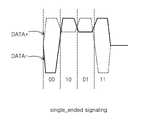
상기 입력 데이터(Data+,Data-)는 일반적으로 트랜스미터(transmitter)에서 전송한 신호가 채널을 통과한 후 신호이며 리시버 회로에 입력되는 신호이다. 상기 입력 데이터(Data+,Data-)는 페어(pair)로 전송되고, 도 5a에 도시된 바와 같이 입력 데이터(Data+,Data-)의 크기에 따라 00,01,10,11로 구분할 수 있다. 또한 도 5b에 도시된 바와 같이, 디퍼렌셜 신호 방식으로 00,01,10,11로 나타낼 수 있다. 디퍼렌셜 신호 방식이란 상기 입력 데이터(Data+,Data-)의 전압 차이를 갖고 상기 입력 데이터(Data+,Data-)의 정보를 구분하는 것이다. 가장 낮은 신호는 00 이며, 가장 높은 신호는 11이다.The input data (Data +, Data-) is generally a signal transmitted from a transmitter after passing through a channel and input to a receiver circuit. The input data Data + and Data− are transmitted in pairs, and may be divided into 00, 01, 10, and 11 according to sizes of the input data Data + and Data−, as shown in FIG. 5A. In addition, as shown in Figure 5b, it can be represented as 00,01,10,11 in the differential signal method. The differential signal method distinguishes information of the input data Data + and Data- with a voltage difference between the input data Data + and Data-. The lowest signal is 00 and the highest signal is 11.
상기 제1 페이즈 전송부(100)는 제1 내지 제3 레벨 감지부(110~130) 및 제1 코딩부(140)를 포함한다. 상기 제1 페이즈 전송부(100)의 상세 구성에 대해서는 도 2에 도시된 상기 제1 페이즈 전송부(100)에서 기술하겠다.The
상기 제2 페이즈 전송부(200)는 제2 클럭(CLK<2>)에 동기되고 상기 제1 디스차징 조절부(500)의 출력에 따라 상기 입력 데이터(Data+,Data-)를 감지하여 제2 출력 신호(SA_OUT4,SA_OUTB4,,,)를 전송한다. 상기 제2 페이즈 전송부(200)는 제4 내지 제6 레벨 감지부(210~230) 및 제2 코딩부(240)를 포함한다.The
상기 제3 페이즈 전송부(300)는 제3 클럭(CLK<3>)에 동기되고 상기 제2 디스차징 조절부(600)의 출력에 따라 상기 입력 데이터(Data+,Data-)를 감지하여 제3 출력 신호(SA_OUT7,SA_OUTB7,,,)를 전송한다.The
상기 제3 페이즈 전송부(300)는 제7 내지 제9 레벨 감지부(310~330) 및 제3 코딩부(340)를 포함한다.The
상기 제4 페이즈 전송부(400)는 제4 클럭(CLK<4>)에 동기되고 상기 제3 디스차징 조절부(700)의 출력에 따라 상기 입력 데이터(Data+,Data-)를 감지하여 제4 출력 신호(SA_OUT10,SA_OUTB10,,,)를 전송한다.The
상기 제4 페이즈 전송부(400)는 제10 내지 제12 레벨 감지부(410~430) 및 제4 코딩부(440)를 포함한다.The
상기 제1 디스차징 조절부(500)는 상기 제1 출력 신호(SA_OUT1,SA_OUTB1,,,)에 따라 상기 제2 페이즈 전송부(200)의 노드 전위를 변동시켜 상기 제2 페이즈 전송부(200)의 전송 속도를 조절한다.The
상기 제1 디스차징 조절부(500)는 제1 캐패시터부(510), 제2 캐패시터부(520) 및 제3 캐패시터부(530)를 포함한다. 상기 제1 캐패시터부(510)는 상기 제1 레벨 감지부(110)의 출력과 상기 제4 레벨 감지부(210) 노드에 연결된다. 상기 제2 캐패시터부(520)는 상기 제2 레벨 감지부(120)의 출력과 상기 제5 레벨 감지부(220)의 노드에 연결된다. 상기 제3 캐패시터부(530)는 상기 제3 레벨 감지부(130)의 출력과 상기 제6 레벨 감지부(230)의 노드에 연결된다.The first discharging adjusting
상기 제2 디스차징 조절부(600)는 상기 제2 출력 신호(SA_OUT4,SA_OUTB4,,,)를 입력받아 상기 제3 페이즈 전송부(300)의 노드 전위를 변동시켜 상기 제3 페이즈 전송부(300)의 전송 속도를 조절한다. 상기 제2 디스차징 조절부(600)는 제4 캐패시터부(610), 제5 캐패시터부(620) 및 제6 캐패시터부(630)를 포함한다. 상기 제4 내지 제6 캐패시터부(610~630)는 각각 제4 내지 제6 레벨 감지부(210~230)의 출력과 제7 내지 제9 레벨 감지부(310~330)의 노드에 연결된다.The
상기 제3 디스차징 조절부(700)는 상기 제3 출력 신호(SA_OUT7,SA_OUTB7,,,)를 입력받아 상기 제4 페이즈 전송부(400)의 노드 전위를 변동시켜 상기 제4 페이즈 전송부(400)의 전송 속도를 조절한다. 상기 제3 디스차징 조절부(700)는 제7 캐패시터부(710), 제8 캐패시터부(720) 및 제9 캐패시터부(730)를 포함한다. 상기 제7 내지 제9 캐패시터부(730)는 각각 상기 제7 내지 제9 레벨 감지부(310~330)의 출력과 제10 내지 제12 레벨 감지부(410~430)의 노드에 연결된다.The third discharging controller 700 receives the third output signal SA_OUT7, SA_OUTB7,, and changes the node potential of the
상기 제4 디스차징 조절부(800)는 상기 제4 출력 신호(SA_OUT10 SA_OUTB10,,,)를 입력받아 상기 제1 페이즈 전송부(100)의 노드 전위를 변동시켜 상기 제1 페이즈 전송부(100)의 전송 속도를 조절한다. 상기 제4 디스차징 조절부(800)는 제10 캐패시터부(810), 제11 캐패시터부(820) 및 제12 캐패시터부(830)를 포함한다. 상기 제10 내지 제12 캐패시터부(810~830)는 각각 상기 제10 내지 제12 레벨 감지부(410~430)의 출력과 제1 내지 제3 레벨 감지부(110~130)의 노드에 연결된다.The
상기 제1 디스차징 조절부(500)는 상기 제1 클럭(CLK<1>)이 인에이블될때의 입력 데이터(Data+,Data-)와 상기 제2 클럭(CLK<2>)이 인에이블될때의 입력 데이터(Data+,Data-)가 다른 레벨이면, 상기 제2 페이즈 전송부(200)의 데이터 전송 속도를 가속시킨다.The
또한, 상기 제1 디스차징 조절부(500)는 상기 제1 클럭(CLK<1>)이 인에이블될때의 입력 데이터(Data+,Data-)와 상기 제2 클럭(CLK<2>)이 인에이블될때의 입력 데이터(Data+,Data-)가 같은 레벨이면, 상기 제2 페이즈 전송부(200)의 데이터 전송 속도를 감속시킨다.In addition, the
상기 제1 내지 제4 디스차징 조절부(500~800)를 구성하는 상기 제1 내지 제12 캐패시터부의 상세 설명은 도 3에 도시된 제1 센스 앰프(10) 및 상기 제10 캐패시터부(810)의 상세 회로도의 설명에서 기술하겠다.Detailed description of the first to twelfth capacitor parts constituting the first to fourth discharging adjusting
도 2는 도 1에 도시된 상기 제1 페이즈 전송부(100)의 상세 블록도이다.FIG. 2 is a detailed block diagram of the
상기 제1 페이즈 전송부(100)는 제1 레벨 감지부(110), 제2 레벨 감지부(120), 제3 레벨 감지부(130) 및 제1 코딩부(140)를 포함한다.The
상기 제1 레벨 감지부(110)는 제1 전압(off<1>,offb<1>)에 따라 상기 입력 데이터(Data+,Data-)에서 제1 레벨 이상의 신호를 감지 및 증폭하여 상기 제1 출력 신호(SA_OUT1,SA_OUTB1,,,) 중 제1 감지 신호(SA_OUT1,SA_OUTB1)를 출력한다. 상기 제1 전압(off<1>,offb<1>)은 상기 제10 캐패시터부(810)의 출력이며, 상기 제1 감지 신호(SA_OUT1,SA_OUTB1)는 상기 제1 캐패시터부(510)에 입력된다.The
상기 제1 레벨 감지부(110)는 제1 센스 앰프(10) 및 제1 래치부(20)를 포함한다.The
상기 제1 센스 앰프(10)는 상기 입력 데이터(Data+,Data-)에서 상기 제1 레벨 이상의 신호를 감지 및 증폭한다.상기 제1 래치부(20)는 상기 제1 감지 신호(SA_OUT1,SA_OUTB1)를 입력받아 래치하여 상기 제1 코딩부(140)로 전송한다.The
상기 제2 레벨 감지부(120)는 제2 전압(off<2>,offb<2>)에 따라 상기 입력 데이터(Data+,Data-)에서 제2 레벨 이상의 신호를 감지 및 증폭하여 상기 제1 출력 신호(SA_OUT1,SA_OUTB1,,,) 중 제2 감지 신호(SA_OUT2,SA_OUTB2)를 출력한다. 상기 제2 전압(off<2>,offb<2>)은 상기 제11 캐패시터부(820)의 출력이며, 상기 제2 감지 신호는 상기 제2 캐패시터부(520)에 입력된다.The
상기 제2 레벨 감지부(120)는 제2 센스 앰프(30) 및 제2 래치부(40)를 포함한다.The
상기 제2 센스 앰프(30)는 상기 입력 데이터(Data+,Data-)에서 상기 제2 레벨 이상의 신호를 감지 및 증폭한다.상기 제2 래치부(40)는 상기 제2 감지 신호(SA_OUT2,SA_OUTB2)를 입력받아 래치하여 상기 제1 코딩부(140)로 전송한다.The
상기 제3 레벨 감지부(130)는 상기 제1 오프셋 전압 중 제3 전압(off<3>,offb<3>)에 따라 상기 입력 데이터(Data+,Data-)에서 제3 레벨 이상의 신호를 감지 및 증폭하여 상기 제1 출력 신호(SA_OUT1,SA_OUTB1,,,) 중 제3 감지 신호(SA_OUT3,SA_OUTB3)를 출력한다. 상기 제3 전압(off<3>,offb<3>)은 상기 제12 캐패시터부(830)의 출력이며, 상기 제3 감지 신호(SA_OUT3,SA_OUTB3)는 상기 제3 캐패시터부(530)에 입력된다.The
상기 제3 레벨 감지부(130)는 제3 센스 앰프(50) 및 제3 래치부(60)를 포함 한다.The
상기 제3 센스 앰프(50)는 상기 입력 데이터(Data+,Data-)에서 상기 제3 레벨 이상의 신호를 감지 및 증폭한다.상기 제3 래치부(60)는 상기 제3 감지 신호(SA_OUT3,SA_OUTB3)를 입력받아 래치하여 상기 제1 코딩부(140)로 전송한다.The
상기 제1 코딩부(140)는 상기 제1 레벨 감지부(110)의 출력(SA_OUT1,SA_OUTB1), 상기 제2 레벨 감지부(120)의 출력(SA_OUT2,SA_OUTB2) 및 상기 제3 레벨 감지부(130)의 출력(SA_OUT3,SA_OUTB3)을 입력받아 코딩하여 제1 페이즈 출력 신호(RXDATA_0<1:0>)를 출력한다.The
도 2에 도시된 상기 제1 페이즈 전송부(100)의 동작을 설명하면 다음과 같다. 상기 제1 내지 제3 센스 앰프(10,30,50)는 상기 제1 클럭(CLK<1>)에 동기되어 구동되고, 상기 데이터(Data+,Data-)를 입력받아 각각 제1 레벨, 상기 제2 레벨, 상기 제3 레벨 이상인 경우 하이 레벨의 신호를, 그 이하인 경우 로우 레벨의 신호를 출력한다. 상기 제1 내지 제3 래치부(20,40,60)는 각각 상기 제1 내지 제3 센스 앰프(10,30,50)의 출력을 래치하여 상기 제1 코딩부(140)로 출력한다.The operation of the
도 3은 상기 제1 센스 앰프(10) 및 상기 제10 캐패시터부(810)의 상세 회로도이다.3 is a detailed circuit diagram of the
상기 제1 센스 앰프(10)는 상기 클럭(CLK)에 동기되어 상기 입력 데이터(Data+,Data-)를 증폭한다.The
상기 센스 앰프(112)는 입력 비교부(11) 및 증폭부(12)를 포함한다.The sense amplifier 112 includes an
상기 입력 비교부(11)는 상기 입력 데이터(Data+,Data-)를 입력받아 제1 노 드(Node_1) 및 제2 노드(Node_2)의 전위를 조절한다. 상기 입력 비교부(11)는 제1,제2 엔모스 트랜지스터(N1~N2) 및 제5 엔모스 트랜지스터(N5)로 구현할 수 있다.The
상기 증폭부(12)는 상기 제1 노드(Node_1) 및 상기 제2 노드(Node_2)의 전위에 따라 상기 제1 감지 신호(SA_OUT1,SA_OUTB1)를 증폭시킨다. 상기 증폭부(12)는 제3, 제4 엔모스 트랜지스터(N3,N4), 제3,제4 피모스 트랜지스터(P3,P4), 제1,제2 피모스 트랜지스터(P1,P2) 및 제5 내지 제7 피모스 트랜지스터(P5~P7)로 구현할 수 있다.The
또한, 상기 제10 캐패시터부(810)는 상기 제10 레벨 감지부(410)의 출력(SA_OUT10,SA_OUTB10)과 제1 레벨 감지부(110) 내의 상기 제1 센스 앰프(10)와 연결된다.In addition, the
상기 제10 캐패시터부(810)는 모스 캐패시터(C1) 및 모스 캐패시터(C2)로 구현할 수 있다. 상기 모스 캐패시터(C1) 는 게이트가 상기 제1 노드(Node_1)에 연결되고, 드레인 및 소스는 상기 제10 레벨 감지부(410)의 출력(SA_OUT10,SA_OUTB10)에 연결된다. 또한, 상기 모스 캐패시터(C2)는 게이트가 상기 제2 노드(Node_2)에 연결되고, 드레인 및 소스는 상기 제10 레벨 감지부(410)의 출력(SA_OUT10,SA_OUTB10)에 연결된다.The
도 1에 도시된 상기 제2 내지 제12 센스 앰프의 구성은 도 3에 도시된 상기 제1 센스 앰프(10)의 구성과 같고, 입력받는 캐패시터부의 출력, 클럭 및 출력 신호가 다를 뿐이다.The configuration of the second to twelfth sense amplifiers illustrated in FIG. 1 is the same as that of the
또한, 상기 제1 내지 제9 캐패시터부, 상기 제11 캐패시터부 및 상기 제12 캐패시터부의 구성 또한 상기 제10 캐패시터부(810)와 같이 모스 캐패시터에 의해 구현할 수 있다.In addition, the first to ninth capacitor parts, the eleventh capacitor part, and the twelfth capacitor part may also be implemented by a MOS capacitor like the
도 3에 도시된 상기 제1 센스 앰프(10) 및 상기 제10 캐패시터부(810)의 동작을 설명하면 다음과 같다.An operation of the
상기 클럭 신호(CLK)가 디스에이블됨에 따라 상기 제1 피모스 트랜지스터(P1) 및 상기 제2 피모스 트랜지스터(P2)가 턴온되므로, 상기 제1 감지 신호(SA_OUT1,SA_OUTB1)는 하이 레벨로 프리차징된다.Since the first PMOS transistor P1 and the second PMOS transistor P2 are turned on as the clock signal CLK is disabled, the first sensing signals SA_OUT1 and SA_OUTB1 are precharged to a high level. do.
상기 클럭 신호(CLK)가 인에이블됨에 따라 상기 제5 엔모스 트랜지스터(N5)가 턴온되므로, 상기 제1 센스 앰프(10)의 전류 패스가 형성되고, 상기 입력 데이터(Data+,Data-)의 크기에 따라 증폭된 제1 감지 신호(SA_OUT1,SA_OUTB1)가 출력된다.Since the fifth NMOS transistor N5 is turned on as the clock signal CLK is enabled, a current path of the
상기 입력 데이터(Data+,Data-)가 하이, 로우 레벨이면, 상기 제1 엔모스 트랜지스터(N1)가 턴온되므로, 상기 제1 노드(Node_1)의 전위가 로우 레벨이 되고, 상기 제2 노드(Node_2)의 전위가 하이 레벨이 된다. 따라서, 상기 제3 엔모스 트랜지스터(N3)의 게이트-소스 전압차는 상기 제4 엔모스 트랜지스터(N4)의 게이트-소스 전압차보다 크므로, 상기 제1 감지 신호(SA_OUT1,SA_OUTB1)는 하이,로우 레벨이 된다.When the input data Data + and Data− are high and low levels, the first NMOS transistor N1 is turned on, so that the potential of the first node Node_1 becomes low level and the second node Node_2. ) Is at the high level. Therefore, since the gate-source voltage difference of the third NMOS transistor N3 is greater than the gate-source voltage difference of the fourth NMOS transistor N4, the first sensing signals SA_OUT1 and SA_OUTB1 are high and low. It becomes a level.
그런데, 상기 제1 센스 앰프(10)는 상기 상기 제10 레벨 감지부(410)의 출력(SA_OUT10,SA_OUTB10)에 의해 상기 제1 노드(Node_1) 및 상기 제2 노드(Node_2)의 전위는 변동될 수 있다. 예를 들면, 상기 상기 제10 레벨 감지부(410)의 출 력(SA_OUT10,SA_OUTB10)이 하이, 로우 레벨이고, 상기 입력 데이터(Data+,Data-)는 하이, 로우 레벨일 때, 프리차징시 상기 제1 노드(Node_1)의 전위 및 상기 제2 노드(Node_2)의 전위는 하이 레벨이고, 상기 캐패시터(C1,C2)는 엔모스 트랜지스터에 의해 구현한 캐패시터이므로, 상기 모스 캐패시터(C1)는 양단이 하이,하이 레벨이므로 상기 센스 앰프(10)에 영향을 주지 않고, 상기 모스 캐패시터(C2)는 게이트단은 하이 레벨이고, 드레인 및 소스단은 로우 레벨이므로 캐패시터로 동작하여 상기 제1 센스 앰프(10)가 프리차징 이후의 동작에 영향을 준다. 즉, 상기 제1 센스 앰프(10)가 구동할 때, 상기 제2 노드(Node_2)의 전위는 상기 모스 캐패시터에 의해 하이 레벨의 전위를 유지하려고 하고 있고, 상기 제1 노드(Node_1)의 전위는 하이 레벨의 입력 데이터(Data+)에 의해 로우 레벨로 디스차징되므로, 상기 센스 앰프(112)는 상기 제1 노드(Node_1)와 상기 제2 노드(Node_2)의 전위차에 의해 빠르게 증폭할 수 있다.However, in the
상기 제10 캐패시터부(810)에 의해, 상기 상기 제10 캐패시터부(810)가 없는 경우보다 상기 제1 센스 앰프(10)의 구동 속도가 증가한다.The driving speed of the
만약, 상기 제10 레벨 감지부(410)의 출력(SA_OUT10,SA_OUTB10)이 로우, 하이 레벨이고, 상기 입력 데이터(Data+,Data-)는 하이, 로우 레벨이면, 위의 경우와 반대로 상기 모스 캐패시터(C1)의 양단은 하이, 로우 레벨이고, 상기 모스 캐패시터(C2)의 양단은 하이, 하이 레벨이므로, 상기 모스 캐패시터(C1)만이 상기 제1 센스 앰프(10)에 영향을 주게 된다. 따라서, 상기 제1 노드(Node_1) 의 전위는 상기 모스 캐패시터에 의해 하이 레벨로 유지하려고 하며, 상기 제2 노드(Node_2)의 전 위는 상기 입력 데이터(Data-)에 의해 변동된다.If the outputs SA_OUT10 and SA_OUTB10 of the
또한, 상기 제10 캐패시터부(810)의 크기 즉, 캐패시턴스에 따라 상기 제1 노드(Node_1) 및 상기 제2 노드(Node_2)의 전위가 상기 제10 레벨 감지부(410)의 출력(SA_OUT10,SA_OUTB10)에 의해 영향을 받는 정도는 달라지게 된다.In addition, the potentials of the first node Node_1 and the second node Node_2 are determined by the size of the
도 1 내지 도 3을 참조하여 본 발명에 따른 리시버 회로의 동작을 설명하면 다음과 같다.Referring to Figures 1 to 3 the operation of the receiver circuit according to the present invention will be described.
먼저, 도 1에 도시되어 있듯이, 본 발명에 따른 리시버 회로는 4개의 다른 위상을 갖는 클럭에 따라 동작함을 가정한다. 즉, 제1 클럭 내지 제4 클럭(CLK<1:4>)은 각기 0도, 90도, 180도, 270도에서 인에이블되는 클럭이다. 또한, 입력 데이터(Data+)는 1101000 패턴으로 상기 리시버 회로에 입력된다고 가정한다.First, as shown in Fig. 1, it is assumed that the receiver circuit according to the present invention operates according to a clock having four different phases. That is, the first to fourth clocks CLK <1: 4> are clocks enabled at 0 degrees, 90 degrees, 180 degrees, and 270 degrees, respectively. In addition, it is assumed that input data Data + is input to the receiver circuit in a 1101000 pattern.
상기 제1 내지 제12 센스 앰프는 상기 제1 내지 제4 클럭(CLK<1:4>)이 각각 반주기 동안 인에이블되고, 반주기 동안 디스에이블되므로, 인에이블되는 구간인 반주기 동안은 각각 센싱 및 증폭 동작을 수행하고, 그 신호를 유지한다.In the first to twelfth sense amplifiers, the first to fourth clocks CLK <1: 4> are enabled for half a period and are disabled for half a period, respectively. Perform an action and keep that signal.
또한, 상기 제1 내지 제12 캐패시터부는 도 3에 도시된 상기 제10 캐패시터부(810)의 구성과 같이 엔모스 캐패시터에 의해 구현한다.In addition, the first to twelfth capacitor parts are implemented by NMOS capacitors as in the configuration of the
또한, 상기 제1 내지 제4 페이즈 전송부(100~400)는 각각 제1 내지 제3 레벨 감지부(110,120,130), 제4 내지 제6 레벨 감지부(210,220,230), 제7 내지 제9 레벨 감지부(310,320,330), 및 제10 내지 제12 레벨 감지부(410,420,430)에 의해 상기 입력 데이터 (Data+,Data-)를 상기 복수의 레벨(제1,제2,제3 레벨)에 의해 감지한다. 이 중 상기 입력 데이터(Data+,Data-)를 복수의 레벨에 따라 감지하여 전송하 는 동작의 설명은 생략하고(도 2 참조), 그 중 제1 레벨을 감지하여 데이터를 출력하는 상기 제1 내지 제4 클럭 (CLK<1:4>)에 따른 상기 제1,4,7,10 레벨 감지부(110,210,310,410) 및 상기 제1,4,7,10 캐패시터부(510,610,710,810)에 의한 동작을 설명하면 다음과 같다.In addition, the first to
상기 제1 클럭(CLK<1>)이 인에이블되고, 상기 제1 센스 앰프(10)는 하이, 로우 레벨의 상기 입력 데이터(Data+,Data-)를 감지 및 증폭하여 하이, 로우 레벨의 상기 제1 감지 신호(SA_OUT1,SA_OUTB1)를 출력한다. 이때, 하이, 로우 레벨의 상기 제1 센스 앰프(10)의 출력(SA_OUT1, SA_OUTB1)은 상기 제1 캐패시터부(510)로 하이, 로우 레벨이 입력된다. 따라서, 상기 제1 캐패시터부(상기 제10 캐패시터부와 같은 구조를 갖고 있다고 가정한다)의 제1 모스 캐패시터(C1)는 하이 레벨을 입력받고, 제2 모스 캐패시터(C2)는 로우 레벨을 입력받는다.The first clock CLK <1> is enabled, and the
그 후, 상기 제2 클럭(CLK<2>)이 인에이블되고, 상기 제4 센스 앰프(제1 센스 앰프와 같은 구조를 갖고 있다고 가정한다)는 하이, 로우 레벨의 입력 데이터 (Data+,Data-)를 입력는다. 이 경우, 상기 입력 데이터(Data+,Data-)가 상기 제1 클럭(CLK<1>)이 인에이블될 때의 입력 데이터(Data+,Data-)와 같은 레벨을 갖고 있는 경우다. 상기 데이터(Data+)가 하이 레벨이므로 제1 엔모스 트랜지스터(N1)가 턴온되므로 상기 제1 노드(Node_1)의 전위는 로우 레벨이 되고, 제2 엔모스 트랜지스터(N2)가 턴오프되므로 상기 제2 노드(Node_2)의 전위는 하이 레벨이 된다. 이 때, 상기 제1 캐패시터부(510)의 제2 캐패시터(C2)의 한 단자가 로우 레벨이므로, 상기 제2 노드(Node_2)의 전위는 하이 레벨에서 조금씩 낮아진다. 따라서, 상기 제 4 센스 앰프의 구동 속도는 느려지지만, 이전 입력 데이터 (Data+,Data-) 또한 하이, 로우 레벨로 변동이 없는 경우이므로, 데이터의 전송에는 문제가 없다. 상기 제4 센스 앰프는 하이, 로우 레벨의 제4 감지 신호(SA_OUT4,SA_OUTB4)를 출력한다.Thereafter, the second clock CLK <2> is enabled, and the fourth sense amplifier (assuming that it has the same structure as the first sense amplifier) has high and low level input data (Data +, Data-). Enter). In this case, the input data Data + and Data− have the same level as the input data Data + and Data− when the first clock CLK <1> is enabled. Since the first NMOS transistor N1 is turned on because the data Data + is high level, the potential of the first node Node_1 is turned low, and the second NMOS transistor N2 is turned off, so that the second NMOS transistor N1 is turned on. The potential of the node Node_2 is at a high level. At this time, since one terminal of the second capacitor C2 of the first capacitor unit 510 is at the low level, the potential of the second node Node_2 is slightly lowered at the high level. Therefore, although the driving speed of the fourth sense amplifier is slow, the previous input data (Data +, Data-) is also a case where there is no change in the high and low levels, so there is no problem in data transmission. The fourth sense amplifier outputs fourth sensing signals SA_OUT4 and SA_OUTB4 having high and low levels.
이때, 하이, 로우 레벨의 상기 제4 센스 앰프의 출력(SA_OUT4, SA_OUTB4)은 상기 제4 캐패시터부(410)로 하이, 로우 레벨이 입력된다. 따라서, 상기 제4 캐패시터부(상기 제10 캐패시터부와 같은 구조를 갖고 있다고 가정한다)의 제1 모스 캐패시터(C1)는 하이 레벨을 입력받고, 제2 모스 캐패시터(C2)는 로우 레벨을 입력받는다.In this case, high and low levels of the outputs SA_OUT4 and SA_OUTB4 of the fourth sense amplifiers having high and low levels are input to the
그 후, 상기 제3 클럭(CLK<3>)이 인에이블되고, 상기 제7 센스 앰프(제1 센스 앰프와 같은 구조를 갖고 있다고 가정한다)는 로우, 하이 레벨의 입력 데이터 (Data+,Data-)를 입력받는다. 이 경우, 상기 입력 데이터(Data+,Data-)가 상기 제1 클럭(CLK<2>)이 인에이블될 때의 입력 데이터(Data+,Data-)와 다른 레벨을 갖고 있는 경우다. 상기 데이터(Data+)가 로우 레벨이므로 제2 엔모스 트랜지스터(N2)가 턴온되므로 상기 제2 노드(Node_2)의 전위는 로우 레벨이 되고, 제1 엔모스 트랜지스터(N1)가 턴오프되므로 상기 제1 노드(Node_1)의 전위는 하이 레벨이 된다. 이 때, 상기 제4 캐패시터부(610)의 제2 캐패시터(C2)의 한 단자가 로우 레벨이므로, 상기 제2 노드(Node_2)의 전위는 로우 레벨에서 더욱 더 로우 레벨로 낮아진다. 따라서, 상기 제7 센스 앰프의 구동 속도는 빨라지므로 이전 입력 데이터 (Data+,Data-)가 하이, 로우 레벨이고, 이번 입력 데이터 (Data+,Data-)가 로우, 하이 레벨로 전압 레벨의 변동이 있음에도, 상기 제7 센스 앰프의 구동 속도의 상 승으로 보다 정확한 데이터를 전송할 수 있다.Thereafter, the third clock CLK <3> is enabled, and the seventh sense amplifier (assuming that it has the same structure as the first sense amplifier) has low and high level input data (Data +, Data-). ) Is inputted. In this case, the input data (Data +, Data-) has a different level than the input data (Data +, Data-) when the first clock (CLK <2>) is enabled. Since the data N + is at the low level, since the second NMOS transistor N2 is turned on, the potential of the second node Node_2 is at a low level, and since the first NMOS transistor N1 is turned off, the first NMOS transistor N2 is turned on. The potential of the node Node_1 is at a high level. At this time, since one terminal of the second capacitor C2 of the fourth capacitor unit 610 is at the low level, the potential of the second node Node_2 is lowered from the low level to a lower level. Therefore, since the driving speed of the seventh sense amplifier is faster, the previous input data (Data +, Data-) is at a high level and a low level. As the driving speed of the seventh sense amplifier increases, more accurate data may be transmitted.
따라서, 그 전의 신호와 이번 신호가 같은 레벨인 경우에는 상기 센스 앰프의 구동 속도를 감속시키고, 그 전의 신호와 이번 신호가 다른 레벨인 경우에는 상기 센스 앰프의 구동 속도를 가속시킴으로써 데이터 전송시의 고속에서의 데이터의 왜곡 현상을 감소시킬 수 있다.Therefore, when the previous signal and the current signal are at the same level, the driving speed of the sense amplifier is decelerated, and when the previous signal and the current signal are at different levels, the driving speed of the sense amplifier is accelerated to speed up the data transfer. This can reduce the distortion of data in the system.
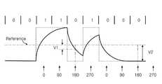
따라서, 도 4a에 나타난 종래 기술에 나타난 레퍼런스 전압 마진(V1)에 비해 도4b에 나타난 본 발명에 따른 리시버 회로의 감지 기준 전압 마진(V1)이 증가됨을 알 수 있다.Accordingly, it can be seen that the sensing reference voltage margin V1 of the receiver circuit according to the present invention shown in FIG. 4B is increased compared to the reference voltage margin V1 shown in the related art shown in FIG. 4A.
즉, 본 발명은 상기 캐패시터의 로딩 효과로 각각의 센스 앰프의 하이 레벨/로우 레벨의 디텍팅을 효과적으로 할 수 있다. 즉, 도 4b에 도시된 바와 같이, 고정된 레퍼런스가 아닌 오프셋 전압에 따라 변동되는 감지 기준 전압 전위(offset controlled Reference)처럼 나타나 신호의 전송시 왜곡되는 점을 감소시킬 수 있다.That is, the present invention can effectively detect the high level / low level of each sense amplifier by the loading effect of the capacitor. That is, as shown in FIG. 4B, it may appear as an offset controlled reference that is changed according to an offset voltage rather than a fixed reference, thereby reducing a distortion point when transmitting a signal.
도 4b에 도시된 본 발명에 따른 리시버에서의 타이밍도에 나타나듯이, 감지 기준 전압의 전위가 이전 입력 데이터에 의한 출력 데이터의 레벨에 따라 상승했다가 하강하는 점을 알 수 있다. 이로 인해, 입력 데이터가 하이 레벨에서 로우 레벨 순으로 입력되는 것과 같이, 입력 데이터의 레벨이 변화되서 전송되는 경우에 갑자기 레벨의 변화시, 전송 마진이 부족한 점을 해결할 수 있다.As shown in the timing diagram of the receiver according to the present invention shown in FIG. 4B, it can be seen that the potential of the sensing reference voltage rises and falls according to the level of the output data by the previous input data. Therefore, it is possible to solve the problem that the transmission margin is insufficient when the level suddenly changes when the level of the input data is changed and transmitted such that the input data is input in the order of the high level to the low level.
도 1 내지 도 3에 도시된 리시버는 이와 같은 방식으로 데이터를 전송함으로써, 데이터의 왜곡없이 전송할 수 있다. 또한, 모스 캐패시터를 사용하여 간단히 구현하므로 어떤 회로에든지 쉽게 적용할 수 있고, 회로 면적이 감소되는 효과가 있다.The receiver shown in FIGS. 1 to 3 transmits data in such a manner so that the receiver can transmit the data without distortion. In addition, since it is simply implemented using a MOS capacitor, it can be easily applied to any circuit, and the circuit area is reduced.
이와 같이, 본 발명에 따른 리시버 회로는 클럭의 위상차가 90도 간격일 때마다 데이터를 전송할 수 있어 고속 데이터의 전송이 가능하다. 또한, 본 발명은 4 페이즈 구조로 설명하였지만, 페이즈 수(클럭 수)에 한정되지 않는다.As described above, the receiver circuit according to the present invention can transmit data whenever the phase difference of the clock is 90 degrees apart, thereby enabling high-speed data transmission. In addition, although the present invention has been described in a four-phase structure, the present invention is not limited to the number of phases (clock number).
본 발명에 따른 리시버 회로는 고속 데이터 전송 시스템의 모든 분야, 메모리, CPU, ASIC 등 다양한 분야에 적용될 수 있다. 또한, 본 발명에 따른 리시버 회로는 4개의 서로 위상이 다른 클럭을 기준으로 신호를 감지하였으나, 클럭의 수에 제한없이 적용될 수 있다.The receiver circuit according to the present invention can be applied to all fields of a high speed data transfer system, various fields such as a memory, a CPU, an ASIC, and the like. In addition, although the receiver circuit according to the present invention senses a signal based on four different phase clocks, it can be applied without limitation to the number of clocks.
이와 같이, 본 발명이 속하는 기술분야의 당업자는 본 발명이 그 기술적 사상이나 필수적 특징을 변경하지 않고서 다른 구체적인 형태로 실시될 수 있다는 것을 이해할 수 있을 것이다.As such, those skilled in the art will appreciate that the present invention can be implemented in other specific forms without changing the technical spirit or essential features thereof.
그러므로 이상에서 기술한 실시예들은 모든 면에서 예시적인 것이며 한정적인 것이 아닌 것으로서 이해해야만 한다. 본 발명의 범위는 상기 상세한 설명보다는 후술하는 특허청구범위에 의하여 나타내어지며, 특허청구범위의 의미 및 범위 그리고 그 등가개념으로부터 도출되는 모든 변경 또는 변형된 형태가 본 발명의 범위에 포함되는 것으로 해석되어야 한다.Therefore, the above-described embodiments are to be understood as illustrative in all respects and not as restrictive. The scope of the present invention is shown by the following claims rather than the detailed description, and all changes or modifications derived from the meaning and scope of the claims and their equivalents should be construed as being included in the scope of the present invention. do.
도 1은 본 발명에 따른 리시버 회로의 블록도,1 is a block diagram of a receiver circuit in accordance with the present invention;
도 2는 도 1에 도시된 상기 제1 페이즈 전송부의 상세 회로도,FIG. 2 is a detailed circuit diagram of the first phase transmitter shown in FIG. 1;
도 3은 도 1에 도시된 제10 캐패시터부 및 제1 센스 앰프의 상세 회로도,3 is a detailed circuit diagram of a tenth capacitor unit and a first sense amplifier shown in FIG. 1;
도 4는 도 1 내지 도 3에 도시된 리시버 회로의 데이터 파형도,4 is a data waveform diagram of a receiver circuit shown in FIGS. 1 to 3;
도 5는 4PAM의 신호 레벨을 나타낸 파형도이다.5 is a waveform diagram showing a signal level of 4PAM.
<도면의 주요 부분에 대한 부호 설명><Description of the symbols for the main parts of the drawings>
100,200,300,400 : 제1,제2,제3,제4 페이즈 전송부100,200,300,400: 1st, 2nd, 3rd, 4th phase transmitter
500,600,700,800 : 제1,제2,제3,제4 디스차징 조절부500,600,700,800: 1st, 2nd, 3rd, 4th discharging control part
110,120,130 : 제1,제2,제3 레벨 감지부110, 120, 130: first, second, third level detector
510,520,530 : 제1,제2,제3 캐패시터부510,520,530: first, second and third capacitor parts
810,820,830 : 제10,제11,제12 캐패시터부810,820,830: 10th, 11th, 12th capacitor part
10,30,50 : 제1,제2,제3 센스 앰프10,30,50: 1st, 2nd, 3rd sense amplifier
20,40,60 : 제1,제2,제3 래치부20,40,60: 1st, 2nd, 3rd latch part
140,240,340,440 : 제1,제2,제3,제4 코딩부140,240,340,440: first, second, third, fourth coding unit
11 : 입력 비교부 12 : 증폭부11
Claims (14)
Translated fromKoreanPriority Applications (2)
| Application Number | Priority Date | Filing Date | Title |
|---|---|---|---|
| KR1020070113097AKR100897282B1 (en) | 2007-11-07 | 2007-11-07 | Receiver circuit |
| US12/170,254US8045647B2 (en) | 2007-11-07 | 2008-07-09 | Low power, high speed receiver circuit for use in a semiconductor integrated circuit |
Applications Claiming Priority (1)
| Application Number | Priority Date | Filing Date | Title |
|---|---|---|---|
| KR1020070113097AKR100897282B1 (en) | 2007-11-07 | 2007-11-07 | Receiver circuit |
Publications (2)
| Publication Number | Publication Date |
|---|---|
| KR20090047089A KR20090047089A (en) | 2009-05-12 |
| KR100897282B1true KR100897282B1 (en) | 2009-05-14 |
Family
ID=40588078
Family Applications (1)
| Application Number | Title | Priority Date | Filing Date |
|---|---|---|---|
| KR1020070113097AExpired - Fee RelatedKR100897282B1 (en) | 2007-11-07 | 2007-11-07 | Receiver circuit |
Country Status (2)
| Country | Link |
|---|---|
| US (1) | US8045647B2 (en) |
| KR (1) | KR100897282B1 (en) |
Families Citing this family (10)
| Publication number | Priority date | Publication date | Assignee | Title |
|---|---|---|---|---|
| TWI501558B (en) | 2012-11-13 | 2015-09-21 | Ind Tech Res Inst | Latch apparatus and applications thereof |
| US10878858B2 (en)* | 2019-02-14 | 2020-12-29 | Micron Technology, Inc. | Apparatuses including input buffers and methods for operating input buffers |
| KR102835912B1 (en) | 2020-08-31 | 2025-07-22 | 삼성전자주식회사 | Multi-level signal receviver and memory system including the same |
| KR102855061B1 (en)* | 2020-09-02 | 2025-09-04 | 삼성전자주식회사 | Multi-level signal receviver and memory system including the same |
| CN115708156B (en)* | 2021-08-20 | 2025-07-25 | 长鑫存储技术有限公司 | Data transmission circuit and memory |
| KR20230049982A (en) | 2021-10-07 | 2023-04-14 | 삼성전자주식회사 | Receiver with pipeline structure for receiving multi-level signal and memory device including the same |
| KR20230056315A (en) | 2021-10-20 | 2023-04-27 | 삼성전자주식회사 | Receiver for receiving multi-level signal and memory device including the same |
| JP7710460B2 (en) | 2022-07-04 | 2025-07-18 | チャンシン メモリー テクノロジーズ インコーポレイテッド | Data receiving circuit, data receiving system and storage device |
| JP7554280B2 (en) | 2022-07-04 | 2024-09-19 | チャンシン メモリー テクノロジーズ インコーポレイテッド | Data receiving circuit, data receiving system and storage device |
| CN117393009A (en)* | 2022-07-04 | 2024-01-12 | 长鑫存储技术有限公司 | Data receiving circuit, data receiving system and storage device |
Citations (2)
| Publication number | Priority date | Publication date | Assignee | Title |
|---|---|---|---|---|
| KR940025185A (en)* | 1993-04-05 | 1994-11-19 | 프레데릭 얀 스미트 | integrated circuit |
| KR20030061265A (en)* | 2002-01-11 | 2003-07-18 | 삼성전자주식회사 | Receiver circuit of semiconductor integrated circuit |
Family Cites Families (8)
| Publication number | Priority date | Publication date | Assignee | Title |
|---|---|---|---|---|
| JP3420018B2 (en) | 1997-04-25 | 2003-06-23 | 株式会社東芝 | Data receiver |
| JP4197755B2 (en)* | 1997-11-19 | 2008-12-17 | 富士通株式会社 | Signal transmission system, receiver circuit of the signal transmission system, and semiconductor memory device to which the signal transmission system is applied |
| JP2000285687A (en)* | 1999-03-26 | 2000-10-13 | Nec Corp | Semiconductor memory, and method for generating timing of signal activating its internal circuit |
| US6396329B1 (en) | 1999-10-19 | 2002-05-28 | Rambus, Inc | Method and apparatus for receiving high speed signals with low latency |
| US7124221B1 (en) | 1999-10-19 | 2006-10-17 | Rambus Inc. | Low latency multi-level communication interface |
| US7292629B2 (en) | 2002-07-12 | 2007-11-06 | Rambus Inc. | Selectable-tap equalizer |
| JP2007504594A (en)* | 2003-09-05 | 2007-03-01 | ズィーモス テクノロジー,インコーポレイテッド | Dynamic memory, sense amplifier circuit, word line driving circuit, control signal PX driving circuit, signal sensing or restoring method, and leakage current reducing method |
| KR20070014242A (en) | 2005-07-28 | 2007-02-01 | 삼성전자주식회사 | Display substrate and display device having same |
- 2007
- 2007-11-07KRKR1020070113097Apatent/KR100897282B1/ennot_activeExpired - Fee Related
- 2008
- 2008-07-09USUS12/170,254patent/US8045647B2/ennot_activeExpired - Fee Related
Patent Citations (2)
| Publication number | Priority date | Publication date | Assignee | Title |
|---|---|---|---|---|
| KR940025185A (en)* | 1993-04-05 | 1994-11-19 | 프레데릭 얀 스미트 | integrated circuit |
| KR20030061265A (en)* | 2002-01-11 | 2003-07-18 | 삼성전자주식회사 | Receiver circuit of semiconductor integrated circuit |
Also Published As
| Publication number | Publication date |
|---|---|
| US20090116596A1 (en) | 2009-05-07 |
| US8045647B2 (en) | 2011-10-25 |
| KR20090047089A (en) | 2009-05-12 |
Similar Documents
| Publication | Publication Date | Title |
|---|---|---|
| KR100897282B1 (en) | Receiver circuit | |
| KR100995656B1 (en) | Receiver circuit | |
| US9998305B2 (en) | Multi-PAM output driver with distortion compensation | |
| US6396329B1 (en) | Method and apparatus for receiving high speed signals with low latency | |
| US7701257B2 (en) | Data receiver and semiconductor device including the data receiver | |
| KR101368413B1 (en) | DFE circuits for use in semiconductor memory device and method for initializing the same | |
| US7167527B1 (en) | System and method for multi-symbol interfacing | |
| JP4979344B2 (en) | Signal detection circuit | |
| US20130028313A1 (en) | Partial response decision feedback equalizer with distributed control | |
| KR100945788B1 (en) | Data Receivers in Semiconductor Integrated Circuits | |
| KR100870536B1 (en) | High speed interface type semiconductor device, semiconductor system, and method thereof | |
| WO2001050228A2 (en) | Low latency multi-level communication interface | |
| CN111159081A (en) | Signal receiving circuit, and semiconductor device and semiconductor system using the same | |
| KR100897280B1 (en) | Receiver circuit | |
| US20250119138A1 (en) | Receiver circuit, a semiconductor apparatus and a semiconductor system including the receiver circuit | |
| US20160087817A1 (en) | Decision feedback equalizer summation circuit | |
| US6937664B1 (en) | System and method for multi-symbol interfacing | |
| KR100771878B1 (en) | Data receiver using semi-dual voltage reference | |
| KR100892722B1 (en) | Receiver circuit | |
| KR100873626B1 (en) | Data Receivers in Semiconductor Integrated Circuits | |
| KR20090024443A (en) | Receiver circuit |
Legal Events
| Date | Code | Title | Description |
|---|---|---|---|
| A201 | Request for examination | ||
| PA0109 | Patent application | St.27 status event code:A-0-1-A10-A12-nap-PA0109 | |
| PA0201 | Request for examination | St.27 status event code:A-1-2-D10-D11-exm-PA0201 | |
| D13-X000 | Search requested | St.27 status event code:A-1-2-D10-D13-srh-X000 | |
| D14-X000 | Search report completed | St.27 status event code:A-1-2-D10-D14-srh-X000 | |
| E902 | Notification of reason for refusal | ||
| PE0902 | Notice of grounds for rejection | St.27 status event code:A-1-2-D10-D21-exm-PE0902 | |
| P11-X000 | Amendment of application requested | St.27 status event code:A-2-2-P10-P11-nap-X000 | |
| P13-X000 | Application amended | St.27 status event code:A-2-2-P10-P13-nap-X000 | |
| E701 | Decision to grant or registration of patent right | ||
| PE0701 | Decision of registration | St.27 status event code:A-1-2-D10-D22-exm-PE0701 | |
| GRNT | Written decision to grant | ||
| PR0701 | Registration of establishment | St.27 status event code:A-2-4-F10-F11-exm-PR0701 | |
| PR1002 | Payment of registration fee | St.27 status event code:A-2-2-U10-U11-oth-PR1002 Fee payment year number:1 | |
| PG1501 | Laying open of application | St.27 status event code:A-1-1-Q10-Q12-nap-PG1501 | |
| PG1601 | Publication of registration | St.27 status event code:A-4-4-Q10-Q13-nap-PG1601 | |
| PN2301 | Change of applicant | St.27 status event code:A-5-5-R10-R13-asn-PN2301 St.27 status event code:A-5-5-R10-R11-asn-PN2301 | |
| FPAY | Annual fee payment | Payment date:20120424 Year of fee payment:4 | |
| PR1001 | Payment of annual fee | St.27 status event code:A-4-4-U10-U11-oth-PR1001 Fee payment year number:4 | |
| PN2301 | Change of applicant | St.27 status event code:A-5-5-R10-R13-asn-PN2301 St.27 status event code:A-5-5-R10-R11-asn-PN2301 | |
| LAPS | Lapse due to unpaid annual fee | ||
| PC1903 | Unpaid annual fee | St.27 status event code:A-4-4-U10-U13-oth-PC1903 Not in force date:20130507 Payment event data comment text:Termination Category : DEFAULT_OF_REGISTRATION_FEE | |
| PC1903 | Unpaid annual fee | St.27 status event code:N-4-6-H10-H13-oth-PC1903 Ip right cessation event data comment text:Termination Category : DEFAULT_OF_REGISTRATION_FEE Not in force date:20130507 | |
| PN2301 | Change of applicant | St.27 status event code:A-5-5-R10-R13-asn-PN2301 St.27 status event code:A-5-5-R10-R11-asn-PN2301 |