KR100896180B1 - Phase change memory device having a selectively grown phase change layer and a method of manufacturing the same - Google Patents
Phase change memory device having a selectively grown phase change layer and a method of manufacturing the sameDownload PDFInfo
- Publication number
- KR100896180B1 KR100896180B1KR1020070007236AKR20070007236AKR100896180B1KR 100896180 B1KR100896180 B1KR 100896180B1KR 1020070007236 AKR1020070007236 AKR 1020070007236AKR 20070007236 AKR20070007236 AKR 20070007236AKR 100896180 B1KR100896180 B1KR 100896180B1
- Authority
- KR
- South Korea
- Prior art keywords
- layer
- phase change
- lower electrode
- forming
- interlayer insulating
- Prior art date
- Legal status (The legal status is an assumption and is not a legal conclusion. Google has not performed a legal analysis and makes no representation as to the accuracy of the status listed.)
- Active
Links
Images


Classifications
- H—ELECTRICITY
- H10—SEMICONDUCTOR DEVICES; ELECTRIC SOLID-STATE DEVICES NOT OTHERWISE PROVIDED FOR
- H10N—ELECTRIC SOLID-STATE DEVICES NOT OTHERWISE PROVIDED FOR
- H10N70/00—Solid-state devices having no potential barriers, and specially adapted for rectifying, amplifying, oscillating or switching
- H10N70/20—Multistable switching devices, e.g. memristors
- H10N70/231—Multistable switching devices, e.g. memristors based on solid-state phase change, e.g. between amorphous and crystalline phases, Ovshinsky effect
- G—PHYSICS
- G11—INFORMATION STORAGE
- G11C—STATIC STORES
- G11C13/00—Digital stores characterised by the use of storage elements not covered by groups G11C11/00, G11C23/00, or G11C25/00
- G11C13/0002—Digital stores characterised by the use of storage elements not covered by groups G11C11/00, G11C23/00, or G11C25/00 using resistive RAM [RRAM] elements
- G11C13/0004—Digital stores characterised by the use of storage elements not covered by groups G11C11/00, G11C23/00, or G11C25/00 using resistive RAM [RRAM] elements comprising amorphous/crystalline phase transition cells
- H—ELECTRICITY
- H10—SEMICONDUCTOR DEVICES; ELECTRIC SOLID-STATE DEVICES NOT OTHERWISE PROVIDED FOR
- H10B—ELECTRONIC MEMORY DEVICES
- H10B63/00—Resistance change memory devices, e.g. resistive RAM [ReRAM] devices
- H10B63/30—Resistance change memory devices, e.g. resistive RAM [ReRAM] devices comprising selection components having three or more electrodes, e.g. transistors
- H—ELECTRICITY
- H10—SEMICONDUCTOR DEVICES; ELECTRIC SOLID-STATE DEVICES NOT OTHERWISE PROVIDED FOR
- H10N—ELECTRIC SOLID-STATE DEVICES NOT OTHERWISE PROVIDED FOR
- H10N70/00—Solid-state devices having no potential barriers, and specially adapted for rectifying, amplifying, oscillating or switching
- H10N70/011—Manufacture or treatment of multistable switching devices
- H10N70/021—Formation of switching materials, e.g. deposition of layers
- H10N70/023—Formation of switching materials, e.g. deposition of layers by chemical vapor deposition, e.g. MOCVD, ALD
- H—ELECTRICITY
- H10—SEMICONDUCTOR DEVICES; ELECTRIC SOLID-STATE DEVICES NOT OTHERWISE PROVIDED FOR
- H10N—ELECTRIC SOLID-STATE DEVICES NOT OTHERWISE PROVIDED FOR
- H10N70/00—Solid-state devices having no potential barriers, and specially adapted for rectifying, amplifying, oscillating or switching
- H10N70/011—Manufacture or treatment of multistable switching devices
- H10N70/061—Shaping switching materials
- H10N70/066—Shaping switching materials by filling of openings, e.g. damascene method
- H—ELECTRICITY
- H10—SEMICONDUCTOR DEVICES; ELECTRIC SOLID-STATE DEVICES NOT OTHERWISE PROVIDED FOR
- H10N—ELECTRIC SOLID-STATE DEVICES NOT OTHERWISE PROVIDED FOR
- H10N70/00—Solid-state devices having no potential barriers, and specially adapted for rectifying, amplifying, oscillating or switching
- H10N70/801—Constructional details of multistable switching devices
- H10N70/821—Device geometry
- H10N70/826—Device geometry adapted for essentially vertical current flow, e.g. sandwich or pillar type devices
- H—ELECTRICITY
- H10—SEMICONDUCTOR DEVICES; ELECTRIC SOLID-STATE DEVICES NOT OTHERWISE PROVIDED FOR
- H10N—ELECTRIC SOLID-STATE DEVICES NOT OTHERWISE PROVIDED FOR
- H10N70/00—Solid-state devices having no potential barriers, and specially adapted for rectifying, amplifying, oscillating or switching
- H10N70/801—Constructional details of multistable switching devices
- H10N70/881—Switching materials
- H10N70/882—Compounds of sulfur, selenium or tellurium, e.g. chalcogenides
- H10N70/8825—Selenides, e.g. GeSe
- H—ELECTRICITY
- H10—SEMICONDUCTOR DEVICES; ELECTRIC SOLID-STATE DEVICES NOT OTHERWISE PROVIDED FOR
- H10N—ELECTRIC SOLID-STATE DEVICES NOT OTHERWISE PROVIDED FOR
- H10N70/00—Solid-state devices having no potential barriers, and specially adapted for rectifying, amplifying, oscillating or switching
- H10N70/801—Constructional details of multistable switching devices
- H10N70/881—Switching materials
- H10N70/882—Compounds of sulfur, selenium or tellurium, e.g. chalcogenides
- H10N70/8828—Tellurides, e.g. GeSbTe
Landscapes
- Engineering & Computer Science (AREA)
- Manufacturing & Machinery (AREA)
- Chemical & Material Sciences (AREA)
- Crystallography & Structural Chemistry (AREA)
- Semiconductor Memories (AREA)
Abstract
Translated fromKoreanDescription
Translated fromKorean도 1은 본 발명의 제1 실시예에 의한 상변화 메모리 소자의 단면도이다.1 is a cross-sectional view of a phase change memory device according to a first embodiment of the present invention.
도 2는 본 발명의 제2 실시에에 의한 상변화 메모리 소자의 단면도이다.2 is a cross-sectional view of the phase change memory device according to the second embodiment of the present invention.
도 3 내지 도 7은 본 발명의 제1 실시예에 의한 상변화 메모리 소자의 제조 방법을 단계별로 나타낸 단면도들이다.3 to 7 are cross-sectional views illustrating a method of manufacturing a phase change memory device according to a first embodiment of the present invention.
도 8 내지 도 10은 본 발명의 제2 실시예에 의한 상변화 메모리 소자의 제조 방법을 단계별로 나타낸 단면도들이다.8 through 10 are cross-sectional views illustrating a method of manufacturing a phase change memory device according to a second exemplary embodiment of the present invention.
도 11 내지 도 15는 본 발명의 제3 실시예에 의한 상변화 메모리 소자의 제조 방법을 단계별로 나타낸 단면도들이다.11 through 15 are cross-sectional views illustrating a method of manufacturing a phase change memory device according to a third exemplary embodiment of the present invention.
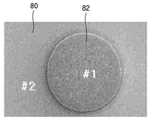
도 16은 본 발명의 제1 실시예에 의한 상변화 메모리 소자에서 씨드층 상에 선택적으로 형성된 GST(Ge2Sb2Te5)층을 보여주는 전자 현미경 사진을 나타낸다.FIG. 16 shows an electron micrograph showing a GST (
도 17은 도 16의 전자 현미경 사진에서 조성 분석을 위해 선택된 영역을 나타낸다.FIG. 17 shows regions selected for compositional analysis in the electron micrograph of FIG. 16.
도 18은 도 17에서 GST층이 형성된 씨드층 상의 제1 지점에 대한 조성 분석 결과를 나타낸 그래프이다.FIG. 18 is a graph illustrating a composition analysis result for the first point on the seed layer on which the GST layer is formed in FIG. 17.
도 19는 도 17에서 GST층이 형성되지 않은 씨드층 둘레의 제2 지점에 대한 조성 분석 결과를 나타낸 그래프이다.FIG. 19 is a graph illustrating a composition analysis result of a second point around a seed layer in which a GST layer is not formed in FIG. 17.
*도면의 주요부분에 대한 부호의 설명** Description of the symbols for the main parts of the drawings *
10:기판 12, 14:제1 및 제2 불순물 영역10:
16:채널영역 18:게이트 절연막16: channel region 18: gate insulating film
19:게이트 전극 20:게이트 적층물19: gate electrode 20: gate stack
22, 32:제1 및 제2 층간 절연층 24:도전성 플러그22, 32: first and second interlayer insulating layer 24: conductive plug
30:하부전극 34:하부전극 콘택층30: lower electrode 34: lower electrode contact layer
36:씨드층(seed layer) 38, 50, 60:상변화층36:
40, 52:절연층 42, 54, 62:상부전극40, 52:
80:실리콘 산화막 82:GST층80: silicon oxide film 82: GST layer
90, 100:피크 G1-G3:제1 내지 제3 피크90, 100: peak G1-G3: first to third peaks
h1, h2:제1 및 제2 콘택홀 P1:상변화층의 돌출부h1, h2: first and second contact holes P1: protrusions of the phase change layer
1. 발명의 분야1. Field of Invention
본 발명은 반도체 메모리 소자에 관한 것으로써, 보다 자세하게는 선택적 성장된 상변화층을 구비하는 상변화 메모리 소자 및 그 제조 방법에 관한 것이다.The present invention relates to a semiconductor memory device, and more particularly, to a phase change memory device having a selectively grown phase change layer and a method of manufacturing the same.
2. 관련기술의 설명2. Description of related technology
상변화 물질(phase change material)은 온도에 따라 결정(crystalline) 상태 또는 비정질(amorphous) 상태를 갖는다. 상변화 물질이 결정 상태일 때의 저항은 비정질 상태일 때의 저항보다 낮다. 상변화 물질의 결정 상태와 비정질 상태는 상호 가역적 변화가 가능하고 명확하게 구분될 수 있다. 이러한 상변화 물질을 메모리 소자에 적용시킨 것이 상변화 메모리 소자(Phase Change Random Access Memory)(이하, PRAM)이다.Phase change materials have a crystalline or amorphous state depending on the temperature. The resistance when the phase change material is in the crystalline state is lower than the resistance when it is in the amorphous state. The crystal state and the amorphous state of the phase change material can be mutually reversible and can be clearly distinguished. Such a phase change material is applied to a memory device, called Phase Change Random Access Memory (hereinafter referred to as PRAM).
PRAM은 일반적으로 트랜지스터의 소스 또는 드레인 영역에 콘택 플러그를 통해 전기적으로 연결된 상변화층을 구비한다. PRAM의 동작은 상변화층의 결정 상태 변화에 따른 저항 차이를 이용하여 수행된다.PRAMs generally have a phase change layer electrically connected through a contact plug to a source or drain region of a transistor. The operation of the PRAM is performed by using the resistance difference according to the change of the crystal state of the phase change layer.
현재까지 소개된 대부분의 PRAM(이하, 종래 PRAM)의 제조 과정에서 스토리지 노드(storage node)는 상변화 물질층인 GST층과 상부전극이 순차적으로 증착된 후, 상기 상부전극과 GST층을 순차적으로 식각하여 형성된다.In the manufacturing process of most PRAMs (hereinafter, referred to as conventional PRAMs) introduced to date, a storage node is sequentially deposited with a phase change material layer, a GST layer, and an upper electrode, and then the upper electrode and the GST layer are sequentially It is formed by etching.
그런데 이와 같은 종래의 PRAM 제조 과정의 경우, 다음과 같은 문제점이 나타날 수 있다.However, in the conventional PRAM manufacturing process, the following problems may occur.
곧, GST층이 식각될 때, GST층의 측면에 데미지(damage)가 발생될 수 있는데, 이러한 데미지는 PRAM의 특성에 치명적인 문제를 일으킬 수 있다. 특히 상대적으로 취약한 GST층과 그 하부막의 계면에 식각가스가 침투될 수 있는데, 이러한 침투는 GST층의 프로그램 영역(program volume), 곧 상변화가 일어나는 영역에 좋지 않은 영향을 줄 수 있다.That is, when the GST layer is etched, damage may occur on the side of the GST layer, which may cause a fatal problem in the characteristics of the PRAM. In particular, the etching gas may penetrate at the interface between the relatively weak GST layer and the lower layer, which may adversely affect the program volume of the GST layer, that is, the region where the phase change occurs.
한편, 종래의 PRAM 중에는 리세트 전류(reset current)를 낮추기 위하여 상 변화층을 콘택홀 안에만 채우는 제한된 구조의 PRAM이 있다. 이와 같은 제한된 구조를 갖는 종래의 PRAM의 경우, 콘택홀을 상변화층으로 채우는 과정에서 오버행(overhang)에 의해 콘택홀의 입구가 막히는 현상이 나타난다. 이에 따라 상변화층에 씸(seam) 혹은 보이드(void)가 형성될 수 있다. 상변화층에 씸이나 보이드가 존재할 경우, 세트 저항이 증가되는 문제가 있다. 또한 씸이나 보이드의 크기와 모양은 셀 별 콘택홀 프로화일(contact profile)의 편차에 따라 민감하게 변하기 때문에, 세트 저항, 리세트 저항, 리세트 전류에 큰 편차를 일으킬 수 있다.On the other hand, in the conventional PRAM, there is a limited structure PRAM in which the phase change layer is filled only in the contact hole in order to lower the reset current. In the conventional PRAM having such a limited structure, the entrance of the contact hole is blocked by overhang during the process of filling the contact hole with the phase change layer. Accordingly, a seam or void may be formed in the phase change layer. In the presence of shock or voids in the phase change layer, there is a problem in that the set resistance is increased. In addition, the size and shape of the pin and void are sensitive to variations in the contact profile of each cell, which can cause large variations in set resistance, reset resistance, and reset current.
본 발명이 이루고자하는 기술적 과제는 상술한 종래 기술의 문제점을 개선하기 위한 것으로서, 상변화층에 식각 데미지가 없고 상변화층에 씸이나 보이드가 포함되지 않은 상변화 메모리 소자를 제공함에 있다.SUMMARY OF THE INVENTION The present invention has been made in an effort to improve the above-described problems of the related art, and to provide a phase change memory device in which the phase change layer has no etch damage and no phase or void is included in the phase change layer.
본 발명이 이루고자 하는 다른 기술적 과제는 이러한 상변화 메모리 소자의 제조 방법을 제공함에 있다.Another object of the present invention is to provide a method of manufacturing such a phase change memory device.
상기 기술적 과제를 달성하기 위하여, 본 발명은 상변화층을 포함하는 스토리지 노드와 이에 연결된 스위칭 소자를 포함하는 상변화 메모리 소자에 있어서, 상기 상변화층은 상기 상변화층의 선택적 성장을 위한 씨드층 상에 구비된 것을 특징으로 하는 상변화 메모리 소자를 제공한다.In order to achieve the above technical problem, the present invention is a phase change memory device including a storage node and a switching element connected to the phase change layer, the phase change layer is a seed layer for the selective growth of the phase change layer It provides a phase change memory device, characterized in that provided on the.
상기 씨드층은 하부전극 상에 구비될 수 있다.The seed layer may be provided on the lower electrode.
상기 하부전극과 상기 씨드층 사이에 하부전극 콘택층이 더 구비될 수 있다.A lower electrode contact layer may be further provided between the lower electrode and the seed layer.
상기 씨드층은 켈코게나이드층, 전기 전도성을 지닌 전이 금속층, 전이 금속 질화물층, 삼원계 질화물층 및 전이 금속 산화물층 중 어느 하나일 수 있다.The seed layer may be any one of a chalcogenide layer, a transition metal layer having electrical conductivity, a transition metal nitride layer, a ternary nitride layer, and a transition metal oxide layer.
또한, 본 발명은 상기 기술적 과제를 달성하기 위하여, 하부전극과 상변화층을 포함하는 스토리지 노드와 이에 연결된 스위칭 소자를 포함하는 상변화 메모리 소자에 있어서,The present invention also provides a phase change memory device including a storage node including a lower electrode and a phase change layer and a switching device connected thereto.
상기 하부전극과 상기 상변화층은 동일 콘택홀에 순차적으로 적층되어 상기 콘택홀을 채운 것을 특징으로 하는 상변화 메모리 소자를 제공한다.The lower electrode and the phase change layer are sequentially stacked in the same contact hole, thereby providing a phase change memory device.
상기 콘택홀은 상기 하부전극의 일부 또는 전체와 상기 상변화층으로 채워진 것일 수 있다.The contact hole may be filled with part or all of the lower electrode and the phase change layer.
상기 하부전극은 상기 콘택홀의 일부를 채우는 하부전극 콘택층; 및 상기 하부전극 콘택층과 상기 스위칭 소자를 연결하는 부분으로 이루어질 수 있다.The lower electrode may include a lower electrode contact layer filling a portion of the contact hole; And a portion connecting the lower electrode contact layer and the switching element.
상기 다른 기술적 과제를 달성하기 위하여, 본 발명은 하부전극 콘택층 상에 상변화층이 구비된 상변화 메모리 소자의 제조 방법에 있어서, 스위칭 소자가 형성된 반도체 기판 상에 상기 스위칭 소자를 덮는 층간 절연막을 형성하는 단계, 상기 스위칭 소자에 접속되는 하부 전극을 형성하는 단계, 상기 하부 전극 상에 하부전극 콘택층을 형성하는 단계 및 상기 하부전극 콘택층 상에 상변화 물질층을 선택적으로 성장시키는 단계를 포함하는 것을 특징으로 하는 상변화 메모리 소자의 제조 방법을 제공한다.In order to achieve the above technical problem, the present invention provides a phase change memory device having a phase change layer on a lower electrode contact layer, the interlayer insulating film covering the switching element on the semiconductor substrate on which the switching element is formed; Forming a lower electrode connected to the switching element, forming a lower electrode contact layer on the lower electrode, and selectively growing a phase change material layer on the lower electrode contact layer. It provides a method for manufacturing a phase change memory device, characterized in that.
본 발명의 실시예에 의하면, 상기 상변화층을 성장시킨 다음, 상기 상변화층의 측면을 감싸는 절연층을 형성하는 단계를 더 포함할 수 있다.According to an embodiment of the present invention, after the growth of the phase change layer, the method may further include forming an insulating layer surrounding a side of the phase change layer.
본 발명의 실시예에 의하면, 상기 하부전극 콘택층과 상기 상변화층 사이에 씨드층을 더 형성하고 상기 씨드층 상에 상기 상변화층을 선택적으로 형성할 수 있다.According to an embodiment of the present invention, a seed layer may be further formed between the lower electrode contact layer and the phase change layer, and the phase change layer may be selectively formed on the seed layer.
상기 절연층을 형성하는 단계는 상기 선택적으로 성장된 상변화층을 덮는 절연층을 형성하는 단계 및 상기 절연층의 상부면을 상기 선택적으로 성장된 상변화층이 노출될 때까지 평탄화하는 단계를 더 포함할 수 있다.The forming of the insulating layer may further include forming an insulating layer covering the selectively grown phase change layer and planarizing an upper surface of the insulating layer until the selectively grown phase change layer is exposed. It may include.
상기 씨드층은 켈코게나이드(chalcogenide)층, 전기 전도성을 지닌 전이 금속층, 전이 금속 질화물층, 삼원계 질화물층 및 전이 금속 산화물층 중 어느 하나로 형성할 수 있다. 이때, 상기 켈코게나이드층은 Ge층, Sb층, Sb2Te3층, GeTe층 및 GeSbTe층 중 어느 하나일 수 있다.The seed layer may be formed of any one of a chalcogenide layer, a transition metal layer having electrical conductivity, a transition metal nitride layer, a ternary nitride layer, and a transition metal oxide layer. In this case, the chalcogenide layer may be any one of a Ge layer, an Sb layer, an
상기 하부전극 콘택층 및 상기 상변화층을 형성하기 전에, 상기 하부전극 콘택층 및 상기 상변화층으로 채워질 콘택홀을 포함하는 상부 층간 절연층을 형성할 수 있다.Before forming the lower electrode contact layer and the phase change layer, an upper interlayer insulating layer including a contact hole to be filled with the lower electrode contact layer and the phase change layer may be formed.
상기 상부 층간 절연층의 콘택홀을 상기 하부전극 콘택층 및 상기 상변화층으로 순차적으로 채운 다음, 상기 상변화층을 대상으로 평탄화 공정을 실시할 수 있다. 상기 평탄화 이후, 상기 절연층 상에 상기 상변화층의 노출된 부분을 덮는 장벽층 및 상부전극을 순차적으로 더 형성할 수 있다.The contact hole of the upper interlayer insulating layer may be sequentially filled with the lower electrode contact layer and the phase change layer, and then a planarization process may be performed on the phase change layer. After the planarization, a barrier layer and an upper electrode covering the exposed portion of the phase change layer may be sequentially formed on the insulating layer.
상기 하부전극 콘택층은 켈코게나이드층, 전기 전도성을 지닌 전이 금속층, 전이 금속 질화물층, 실리사이드층, 삼원계 질화물층 및 전이 금속 산화물층 중 어느 하나로 형성할 수 있다. 이때, 상기 켈코게나이드층은 Ge-Sb-Te-N층, As-Sb-Te- N층, As-Ge-Sb-Te-N층, Sn-Sb-Te-N층, (5A족 원소)-Sb-Te-N층, (6A족 원소)-Sb-Te-N층, (5A족 원소)-Sb-Se-N층 및 (6A족 원소)-Sb-Se-N층 중 어느 하나일 수 있다.The lower electrode contact layer may be formed of any one of a chalcogenide layer, a transition metal layer having electrical conductivity, a transition metal nitride layer, a silicide layer, a ternary nitride layer, and a transition metal oxide layer. At this time, the chalcogenide layer is Ge-Sb-Te-N layer, As-Sb-Te-N layer, As-Ge-Sb-Te-N layer, Sn-Sb-Te-N layer, (Group 5A element Any one of) -Sb-Te-N layer, (Group 6A element) -Sb-Te-N layer, (Group 5A element) -Sb-Se-N layer, and (Group 6A element) -Sb-Se-N layer Can be.
상기 상변화층은 Ge-Sb-Te층, As-Sb-Te층, As-Ge-Sb-Te층, Sn-Sb-Te층, (5A족 원소)-Sb-Te층, (6A족 원소)-Sb-Te층, (5A족 원소)-Sb-Se층 및 (6A족 원소)-Sb-Se층 중 어느 하나일 수 있다.The phase change layer is Ge-Sb-Te layer, As-Sb-Te layer, As-Ge-Sb-Te layer, Sn-Sb-Te layer, (Group 5A element) -Sb-Te layer, (Group 6A element) ) -Sb-Te layer, (group 5A element) -Sb-Se layer and (group 6A element) -Sb-Se layer.
상기 층간 절연막을 형성하기 전에, 상기 스위칭 소자로서 상기 기판 상에 소오스/드레인 및 게이트를 포함하는 트랜지스터를 형성하는 단계, 상기 트랜지스터를 매립하는 하부 층간 절연막을 형성하는 단계, 상기 하부 층간 절연막 내에 상기 소오스 및 드레인과 각각 접속하는 콘택 패드를 형성하는 단계 및 상기 콘택 패드와 상기 하부전극을 전기적으로 연결되는 도전 라인을 형성하는 단계를 더 포함할 수 있다. 상기 도전라인은 도전성 플러그일 수 있다.Before forming the interlayer insulating film, forming a transistor including a source / drain and a gate on the substrate as the switching element, forming a lower interlayer insulating film filling the transistor, and forming the source in the lower interlayer insulating film. And forming contact pads respectively connected to the drains and forming conductive lines electrically connecting the contact pads to the lower electrodes. The conductive line may be a conductive plug.
이러한 본 발명을 이용하면, 선택적 성장을 이용하여 상변화층을 형성하는 바, 상변화층의 측면 식각이 필요하지 않다. 그러므로 상변화층의 측면 식각시에 발생되는 문제점을 해소할 수 있다.By using the present invention, the phase change layer is formed using selective growth, so that side etching of the phase change layer is not required. Therefore, it is possible to solve the problems caused during side etching of the phase change layer.
이하, 본 발명의 실시예에 의한 선택적으로 성장된 상변화층을 포함하는 상변화 메모리 소자 및 그 제조 방법을 첨부된 도면들을 참조하여 상세하게 설명한다. 이 과정에서 도면에 도시된 층이나 영역들의 두께는 명세서의 명확성을 위해 과장되게 도시된 것이다.Hereinafter, a phase change memory device including a phase change layer selectively grown according to an embodiment of the present invention and a method of manufacturing the same will be described in detail with reference to the accompanying drawings. In this process, the thicknesses of layers or regions illustrated in the drawings are exaggerated for clarity.
먼저, 본 발명의 실시예에 의한 상변화 메모리 소자에 대해 설명한다.First, a phase change memory device according to an embodiment of the present invention will be described.
<제1 실시예><First Embodiment>
도 1을 참조하면, 기판(10)에 이격된 제1 및 제2 불순물 영역(12, 14)이 존재한다. 기판(10)은 N 형 또는 P 형 반도체 기판일 수 있다. 제1 및 제2 불순물 영역(12, 14)에 기판(10)에 도핑된 것과 반대되는 타입의 불순물이 도핑되어 있다. 제1 및 제2 불순물 영역(12, 14) 중 하나는 소오스 영역이고, 나머지는 드레인 영역일 수 있다. 제1 및 제2 불순물 영역(12, 14) 사이의 기판(10) 상에 게이트 적층물(20)이 존재한다. 게이트 적층물(20)은 순차적으로 적층된 게이트 절연막(18) 및 게이트 전극(19)을 포함한다. 게이트 적층물(20) 아래의 기판(10)은 채널영역(16)이다. 제1 및 제2 불순물 영역(12, 14), 게이트 적층물(20) 및 채널영역(16)은 스위칭 소자인 트랜지스터를 이룬다. 상기 트랜지스터외의 다른 스위칭 소자, 예를 들면 다이오드가 구비될 수도 있다. 기판(10) 상에 상기 트랜지스터를 덮는 제1 층간 절연층(22)이 형성되어 있다. 제1 층간 절연층(22)에 제2 불순물 영역(14)이 노출되는 제1 콘택홀(h1)이 형성되어 있다. 제1 콘택홀(h1)은 도전성 플러그(24)로 채워져 있다. 제1 층간 절연층(22) 상에 도전성 플러그(24)의 상부면을 덮는 하부전극(30)이 존재한다. 하부전극(30)은 TiN 또는 TiAlN 전극일 수 있다. 하부전극(30)은 또한 금속 이온으로 Ag, Au, Al, Cu, Cr, Co, Ni, Ti, Sb, V, Mo, Ta, Nb, Ru, W, Pt, Pd, Zn 및 Mg로 이루어진 군 중에서 선택된 어느 하나를 포함하는 실리사이드(silicide) 전극일 수 있다. 제1 층간 절연층(22) 상에 하부전극(30)을 덮는 제2 층간 절연층(32)이 형성되어 있다. 제2 층간 절연층(32)은 제1 층간 절연층(22)과 동일할 수 있다. 제2 층간 절연층(32)에 하부전극(30)이 노출되는 제2 콘택홀(h2)이 형성되어 있다. 제2 콘택홀(h2)은 하부전극 콘택층(34)으로 채워져 있 다. 하부전극 콘택층(34)은 제1 전이 금속층, 제1 전이 금속 질화물층, 제1 실리사이드층 및 제1 삼원계 질화물층 중 어느 하나로 형성할 수 있다. 상기 제1 전이 금속층은 Ti층, Zr층, Hf층, V층, Nb층, Ta층 및 W층 중 어느 하나일 수 있다. 그리고 상기 제1 전이 금속 질화물층은 TiN층, ZrN층, HfN층, VN층, NbN층, TaN층 및 WN층 중 어느 하나일 수 있다. 상기 제1 실리사이드층은 전도성을 갖는 것으로서, 예를 들면 CoSi층, TiSi층, Ta-Si층, Ni-Si층일 수 있다. 상기 제1 삼원계 질화물층은 TiAlN층, TaAlN층, TiSiN층, TaSiN층 TiCN층 및 TaCN층 중 어느 하나일 수 있다. 하부전극 콘택층(34)은 캘코게나이드층일 수도 있는데, 예를 들면 Ge-Sb-Te-N층, As-Sb-Te-N층, As-Ge-Sb-Te-N층, Sn-Sb-Te-N층, (5A족 원소)-Sb-Te-N층, (6A족 원소)-Sb-Te-N층, (5A족 원소)-Sb-Se-N층 및 (6A족 원소)-Sb-Se-N층 중 어느 하나일 수 있다.Referring to FIG. 1, there are first and
계속해서, 제2 층간 절연층(32) 상에 하부전극 콘택층(34)의 상부면을 덮는 씨드층(36)이 존재한다. 씨드층(36) 상에는 상변화층(38)이 존재한다. 씨드층(36)과 상변화층(38)은 절연층(40)으로 둘러싸여 있다. 절연층(40) 상에 상변화층(38)의 상부면을 덮는 상부전극(42)이 구비되어 있다. 상부전극(42)과 상변화층(38) 사이에 불순물, 예를 들면 Ti의 확산을 방지하는 확산 장벽층(미도시)이 더 구비될 수 있다.Subsequently, a
씨드층(36)은 켈코게나이드층, 전기 전도성을 지닌 제2 전이 금속층, 제2 전이 금속 질화물층, 제2 삼원계 질화물층 및 전이 금속 산화물층일 수 있다. 이때 상기 켈코게나이드층은 Ge층, Sb층, Sb2Te3층, GeSbTe층, SbTe층 및 GeTe층 중 어 느 하나일 수 있다. 상기 제2 전이 금속층은 Ti층, Zr층, Hf층, V층, Nb층, Ta층 및 W층 중 어느 하나일 수 있다. 상기 제2 전이금속 질화물층은 TiN층, ZrN층, HfN층, VN층, NbN층, TaN층 및 WN층 중 어느 하나일 수 있다. 상기 제2 실리사이드층은 CoSi층, TiSi층, TaSi층, NiSi층 및 GeSi층 중 어느 하나일 수 있다. 상기 제2 삼원계 질화물층은 TiAlN층, TiCN층, TaCN층, TiSiN층 및 TaSiN층 중 어느 하나일 수 있다. 상기 전이 금속 산화물층은 TIO2층, ZrO2층, HfO2층, V2O3층, NbO층, Ta2O5층 및 WO층 중 어느 하나일 수 있다.The
상변화층(38)은 선택적 성장법으로 씨드층(36) 상에만 형성된 것으로 캘코게나이드층일 수 있다. 예를 들면 상변화층(38)은 Ge-Sb-Te층, As-Sb-Te층, As-Ge-Sb-Te층, Sn-Sb-Te층, (5A족 원소)-Sb-Te층, (6A족 원소)-Sb-Te층, (5A족 원소)-Sb-Se층 및 (6A족 원소)-Sb-Se층 중 어느 하나일 수 있다. 상변화층(38)이 Ge-Sb-Te계열의 층일 때, 상변화층(38)은 Ge2Sb2Te5층일 수 있다.The
<제2 실시예>Second Embodiment
스토리지 노드에서 하부전극 콘택층과 상변화층으로 콘택층을 채운데 특징이 있다. 제1 실시예와 동일한 부분에 대해서는 설명을 생략한다.The storage node is characterized by filling the contact layer with the lower electrode contact layer and the phase change layer. The same parts as in the first embodiment will be omitted.
도 2를 참조하면, 제2 콘택홀(h2)의 일부에 하부전극 콘택층(34)이 채워져 있다. 제2 콘택홀(h2)의 나머지 부분은 상변화층(60)으로 채워져 있다. 상변화층(60)은 제1 실시예의 상변화층(38)과 동일한 것일 수 있다. 제2 층간 절연층(32) 상에 상변화층(38)의 노출면을 덮는 상부전극(62)이 존재한다. 상부전극(62)은 선택적 성장법으로 하부전극 콘택층(34) 상에서만 성장된 것으로 상기 제1 실시예의 상부전극(42)과 동일할 수 있다. 하부전극 콘택층(34)은 도전성 플러그(24)와 직접 연결되게 구비될 수 있다. 이 경우, 하부전극 콘택층(34)은 하부전극 역할을 한다. 한편, 하부전극 콘택층(34)을 하부전극(30)의 일부가 제2 콘택홀(h2)로 확장된 것으로 볼 수도 있다. 곧, 하부전극 콘택층(34)과 하부전극(30)을 합하여 상부전극(62)에 대응되는 하부전극으로 간주할 수도 있다.Referring to FIG. 2, the lower
다음에는 본 발명의 실시예에 의한 상변화 메모리 소자의 제조 방법에 대해 설명한다.Next, a method of manufacturing a phase change memory device according to an embodiment of the present invention will be described.
<제1 실시예><First Embodiment>
도 1에 도시한 상변화 메모리 소자를 제조하는 방법을 설명한다.A method of manufacturing the phase change memory device shown in FIG. 1 will be described.
도 3을 참조하면, 기판(10) 상에 게이트 적층물(20)을 형성한다. 게이트 적층물(20)은 게이트 절연막(18)과 게이트 전극(19)을 순차적으로 적층하여 형성한다. 게이트 적층물(20)의 측면에 게이트 스페이서(미도시)가 형성될 수 있다. 기판(10)은 N 타입 또는 P 타입 반도체 기판일 수 있다. 게이트 적층물(20)을 마스크로 하여 기판(10)에 도전성 불순물을 도핑한다. 상기 도전성 불순물은 기판(10)과 반대되는 타입일 수 있다. 상기 도핑에 의해 기판(10)에 이격된 제1 및 제2 불순물 영역(12, 14)이 형성된다. 제1 및 제2 불순물 영역(12, 14) 중 하나는 소오스 영역이고, 나머지는 드레인 영역이다. 기판(10)의 제1 및 제2 불순물 영역(12, 14) 사이의 영역(16)은 채널영역이 된다. 채널영역(16)에는 문턱전압 조절을 위한 불순물이 도핑될 수 있다. 게이트 적층물(20)과 제1 및 제2 불순물 영역(12, 14)은 트랜지스터를 형성할 수 있다. 상기 트랜지스터는 스위칭 소자의 하나인데, 상기 트랜 지스터 대신에 다른 스위칭 소자, 예를 들면 다이오드가 형성될 수 있다.Referring to FIG. 3, a
계속해서, 기판(10) 상에 게이트 적층물(20)을 덮는 제1 층간 절연층(22)을 형성한다. 제1 층간 절연층(22)에 제2 불순물 영역(14)이 노출되는 제1 콘택홀(h1)을 형성한다. 제1 콘택홀(h1)은 제1 불순물 영역(12)이 노출되는 위치에 형성할 수 있다. 도시하지는 않았지만, 제1 콘택홀(h1)과 함께 제1 불순물 영역(12)이 노출되는 콘택홀을 더 형성할 수 있다. 제1 콘택홀(h1)은 도전성 플러그(24)로 채운다. 이때, 제1 콘택홀(h1)과 함께 형성된 상기 콘택홀에도 도전성 플러그(24)가 채워질 수 있다.Subsequently, a first
한편, 제1 콘택홀(h1)을 채운 도전성 플러그(24)와 제2 불순물 영역(14) 사이에 제2 불순물 영역(14)에 연결된 제1 콘택 패드층(미도시)이 형성될 수 있다. 그리고 도전성 플러그(24)는 상기 제1 콘택 패드층 상에 형성될 수 있다.Meanwhile, a first contact pad layer (not shown) connected to the
마찬가지로 상기 도시되지 않은 콘택홀을 채운 도전성 플러그와 제1 불순물 영역(12) 사이에도 제1 불순물 영역(12)에 연결된 제2 콘택 패드층(미도시)이 형성될 수 있다. 이 경우에도 도전성 플러그(24)는 상기 제2 콘택 패드층 상에 형성될 수 있다.Similarly, a second contact pad layer (not shown) connected to the
도전성 플러그(24)를 형성한 다음, 제1 층간 절연층(22) 상에 도전성 플러그(24)의 노출면을 덮는 하부전극(30)을 형성한다. 하부전극(30)은 TiN 또는 TiAlN 전극으로 형성할 수 있다. 하부전극(30)은 또한 금속 이온으로 Ag, Au, Al, Cu, Cr, Co, Ni, Ti, Sb, V, Mo, Ta, Nb, Ru, W, Pt, Pd, Zn 및 Mg로 이루어진 군 중에서 선택된 어느 하나를 포함하는 실리사이드(silicide) 전극으로 형성할 수 있다.After forming the
도 4를 참조하면, 제1 층간 절연층(22) 상에 하부전극(30)을 덮는 제2 층간 절연층(32)을 형성한다. 제1 층간 절연층(22)을 하부 층간 절연층이라할 때, 제2 층간 절연층(32)은 상부 층간 절연층이라 할 수 있다. 제2 층간 절연층(32)은 제1 층간 절연층(22)과 동일한 물질로 형성할 수 있는데, 예를 들면 실리콘 산화막으로 형성할 수 있다. 제2 층간 절연층(32)에 하부전극(30)이 노출되는 제2 콘택홀(h2)을 형성한다. 제2 콘택홀(h2)은 하부전극 콘택층(34)으로 채운다. 하부전극 콘택층(34)은 제1 전이 금속층, 제1 전이 금속 질화물층, 제1 실리사이드층 및 제1 삼원계 질화물층 중 어느 하나로 형성할 수 있다. 상기 제1 전이 금속층은 Ti층, Zr층, Hf층, V층, Nb층, Ta층 및 W층 중 어느 하나일 수 있다. 그리고 상기 제1 전이 금속 질화물층은 TiN층, ZrN층, HfN층, VN층, NbN층, TaN층 및 WN층 중 어느 하나일 수 있다. 상기 제1 실리사이드층은 전도성을 갖는 것으로서, 예를 들면 CoSi층, TiSi층, Ta-Si층, Ni-Si층일 수 있다. 상기 제1 삼원계 질화물층은 TiAlN층, TaAlN층, TiSiN층, TaSiN층 TiCN층 및 TaCN층 중 어느 하나일 수 있다. 하부전극 콘택층(34)은 캘코게나이드층일 수도 있는데, 예를 들면 Ge-Sb-Te-N층, As-Sb-Te-N층, As-Ge-Sb-Te-N층, Sn-Sb-Te-N층, (5A족 원소)-Sb-Te-N층, (6A족 원소)-Sb-Te-N층, (5A족 원소)-Sb-Se-N층 및 (6A족 원소)-Sb-Se-N층 중 어느 하나일 수 있다.Referring to FIG. 4, a second
도 5 이하에서는 제2 층간 절연층(32)과 하부전극(30) 아래에 형성된 적층물은 편의 상 도시하지 않았다.In FIG. 5 and below, the laminate formed under the second
계속해서 도 5를 참조하면, 제2 층간 절연층(32) 상에 하부전극 콘택층(34)을 덮는 씨드층(36)을 형성한다. 이때 씨드층(36)은 하부전극 콘택층(34)과 그 둘 레의 소정 영역의 제2 층간 절연층(32) 상에만 형성한다. 씨드층(36)의 직경에 의해 후속 공정에서 형성되는 상변화층의 직경이 결정된다. 상변화층의 직경은 리세트 전류에 직접적으로 영향을 주는 바, 씨드층(36)을 형성할 때 이점을 고려하여 형성한다. 씨드층(36)은 켈코게나이드(chalcogenide)층, 전기 전도성을 지닌 제2 전이 금속층, 제2 전이 금속 질화물층, 제2 삼원계 질화물층 및 전이 금속 산화물층으로 형성할 수 있다. 상기 켈코게나이드층은 Ge층, Sb층, Sb2Te3층, GeSbTe층, SbTe층 및 GeTe층 중 어느 하나일 수 있다. 상기 제2 전이 금속층은 Ti층, Zr층, Hf층, V층, Nb층, Ta층 및 W층 중 어느 하나일 수 있다. 상기 제2 전이금속 질화물층은 TiN층, ZrN층, HfN층, VN층, NbN층, TaN층 및 WN층 중 어느 하나일 수 있다. 상기 제2 실리사이드층은 CoSi층, TiSi층, TaSi층, NiSi층 및 GeSi층 중 어느 하나일 수 있다. 상기 제2 삼원계 질화물층은 TiAlN층, TiCN층, TaCN층, TiSiN층 및 TaSiN층 중 어느 하나일 수 있다. 상기 전이 금속 산화물층은 TIO2층, ZrO2층, HfO2층, V2O3층, NbO층, Ta2O5층 및 WO층 중 어느 하나일 수 있다.5, a
씨드층(36)을 형성한 다음, 씨드층(36) 상에 상변화층(38)을 선택적으로 형성한다. 상변화층(38)은 유기 금속을 이용하는 화학 기상 증착(MOCVD)법 혹은 원자층 증착(ALD)법으로 형성할 수 있다. 이와 같은 상변화층(38) 형성방법에서 상변화층(38)의 씨드층(36)에 대한 선택성은 씨드층(36) 둘레의 제2 층간 절연층(32)보다 훨씬 높다. 때문에 상변화층(38) 형성 과정에서 상변화층(38)은 씨드층(36) 상에서만 성장된다. 상변화층(38)은 켈코게나이드층일 수 있다. 예를 들면 상변화층(38)은 Ge-Sb-Te층, As-Sb-Te층, As-Ge-Sb-Te층, Sn-Sb-Te층, (5A족 원소)-Sb-Te층, (6A족 원소)-Sb-Te층, (5A족 원소)-Sb-Se층 및 (6A족 원소)-Sb-Se층 중 어느 하나일 수 있다. 상변화층(38)이 Ge-Sb-Te계열의 층일 때, 상변화층(38)은 Ge2Sb2Te5층일 수 있다.After the
상변화층(38)을 소정 높이로 형성한 후, 도 6에 도시한 바와 같이 제2 층간 절연층(32) 상에 상변화층(38)과 씨드층(36)을 덮는 절연층(40)을 씨드층(36)과 상변화층(38)을 합한 두께보다 두껍게 형성한다. 절연층(40)은 실리콘 산화물층일 수 있다. 절연층(40)을 형성한 후, 그 표면을 평탄화한다. 상기 평탄화는, 예를 들면 화학 기계 연마(Chemical Mechanical Polishing)(CMP)방법으로 상변화층(38)이 노출될 때까지 실시할 수 있다.After forming the
도 7을 참조하면, 상기 평탄화 공정을 실시한 후, 평탄화된 절연층(40) 상에 상기 평탄화에 의해 노출된 상변화층(38)을 덮는 상부전극(42)을 형성한다. 상부전극(42)과 상변화층(38) 사이에 확산 장벽층(미도시)을 더 형성할 수 있다. 상기 확산 장벽층은 상부전극(42)에서 상변화층(38)으로 불순물, 예를 들면 Ti가 확산되는 것을 방지한다. 상부전극(42)은, 예를 들면 스퍼터링 증착 방법으로 형성할 수 있다. 이때, 상부전극(42)은, 예를 들면 TiN으로 형성할 수 있다. 상부전극(42), 상변화층(38), 하부전극 콘택층(34), 하부전극(30)은 데이터가 저장되는 부분인 스토리지 노드를 구성한다. 이러한 스토리지 노드에서 하부전극(30)과 하부전극 콘택층(34)은 동일 물질로 형성할 수 있다. 또한 하부전극 콘택층(34)이 직접 제2 불순물 영역(14)에 접촉될 수도 있다.Referring to FIG. 7, after the planarization process is performed, an
상술한 바와 같이, 본 발명의 제1 실시예에 의한 상변화 메모리 소자의 제조 방법은 스토리지 노드 형성 과정에서 상변화층(38)에 대한 식각, 특히 상변화층(38)의 측면 식각 공정이 없다.As described above, the method of manufacturing the phase change memory device according to the first exemplary embodiment of the present invention does not have an etching on the
상부전극(42) 형성 후의 공정은 통상의 제조 방법을 따른다.The process after formation of the
<제2 실시예>Second Embodiment
하부전극 콘택층 상에만 선택적으로 상변화층을 형성하는데 특징이 있다.It is characterized in that the phase change layer is selectively formed only on the lower electrode contact layer.
도 8을 참조하면, 제2 층간 절연층(32)에 제2 콘택홀(h2)을 형성하고, 제2 콘택홀(h2)에 하부전극 콘택층(34)을 채우는 단계까지는 제1 실시예에 따라 진행할 수 있다. 하부전극 콘택층(34)의 재료는 제1 실시예와 동일할 수 있다. 하부전극 콘택층(34)을 형성한 후, 하부전극 콘택층(34) 상에만 선택적으로 상변화층(50)을 형성한다. 상변화층(50)은 제1 실시예의 상변화층(38)과 동일한 재질일 수 있고, 동일한 방법으로 형성할 수 있다.Referring to FIG. 8, the second contact hole h2 is formed in the second
도 9를 참조하면, 제2 층간 절연층(32) 상에 상변화층(50)을 덮는 절연층(52)을 형성한다. 절연층(52)은 제1 실시예의 절연층(40)과 동일한 재료로 형성할 수 있다. 절연층(52)은 상변화층(50)보다 두꺼운 두께로 형성할 수 있다. 이와 같이 절연층(52)을 형성한 다음, 상변화층(50)이 노출될 때까지 절연층(52)의 표면을 평탄화한다.Referring to FIG. 9, an insulating
도 10을 참조하면, 평탄화된 절연층(52) 상에 평탄화에 의해 노출된 상변화층(50)의 노출된 부분을 덮는 상부전극(54)을 형성한다. 상부전극(54)은 제1 실시예의 상부전극(42)과 동일한 재료로 형성할 수 있다.Referring to FIG. 10, the
<제3 실시예>Third Embodiment
콘택홀이 하부전극 콘택층과 상변화층으로 채워진, 도 2에 도시한 상변화 메모리 소자에 대한 제조 방법을 설명한다.A manufacturing method for the phase change memory device shown in FIG. 2, in which contact holes are filled with a lower electrode contact layer and a phase change layer, will be described.
도 11을 참조하면, 제2 층간 절연층(32)에 하부전극(30)이 노출되는 제2 콘택홀(h2)을 형성하는 단계까지는 제1 실시예에 따라 진행할 수 있다. 이때, 제2 층간 절연층(32)은 실리콘 산화물층, 실리콘 질화물층 또는 실리콘 옥시 나이트라이드층(SiON)으로 형성할 수 있다.Referring to FIG. 11, a process of forming the second contact hole h2 exposing the
제2 콘택홀(h2)을 형성한 후, 도 12에 도시한 바와 같이, 제2 콘택홀(h2)의 일부를 하부전극 콘택층(34)으로 채운다. 하부전극 콘택층(34)의 재료는 제1 실시예와 동일할 수 있다.After forming the second contact hole h2, as shown in FIG. 12, a part of the second contact hole h2 is filled with the lower
도 13을 참조하면, 제2 콘택홀(h2)의 나머지를 상변화층(60)으로 채운다. 상변화층(60)은 제1 실시예의 상변화층(38)과 동일한 방법으로 제2 콘택홀(h2)에만 선택적으로 형성할 수 있다. 상변화층(60)을 형성한 후, 상변화층(60)의 제2 층간 절연층(32)의 상부면보다 높게 돌출된 부분(P1)은 평탄화 공정으로 제거한다. 이러한 평탄화 공정 CMP를 이용하여 실시할 수 있다. 상기 평탄화 공정의 결과, 도 14에 도시한 바와 같이, 하부전극 콘택층(60)의 돌출된 부분(P1)은 제거되고 하부전극 콘택층(60)의 노출된 면은 제2 층간 절연층(32)의 상부면과 동일한 높이로 된다.Referring to FIG. 13, the remainder of the second contact hole h2 is filled with the
도 15를 참조하면, 제2 층간 절연층(32) 상에 하부전극 콘택층(60)의 노출된 면을 덮는 상부전극(62)을 형성한다. 상부전극(62)은 제1 실시예의 상부전극(42)과 동일할 수 있다. 이후의 공정은 통상의 제조 방법을 따른다.Referring to FIG. 15, an
상술한 제1 내지 제3 실시예에 의한 상변화 메모리 소자의 제조 방법에서 상변화층(38, 50, 60)이 GST층이고, MOCVD 방법으로 형성할 경우, Ge, Sb 및 Te의 소오스 가스로 각각 (dtbeda)Ge(II), Sb(i-Pr)3 및 Te(t-Bu)2가 사용될 수 있다. 이때의 증착 온도는 220℃∼320℃일 수 있고, 압력은 5토르(torr) 정도일 수 있다.In the manufacturing method of the phase change memory device according to the first to third embodiments described above, the phase change layers 38, 50, and 60 are GST layers, and when formed by the MOCVD method, source gases of Ge, Sb, and Te are used. (Dtbeda) Ge (II), Sb (i-Pr) 3 and Te (t-Bu) 2, respectively, may be used. In this case, the deposition temperature may be 220 ° C. to 320 ° C., and the pressure may be about 5 Torr.
본 발명자는 상기 제1 실시예에 의한 상변화 메모리 소자의 제조 방법에서 설명한 상변화층의 형성 공정에 근거하여 씨드층 상에 상변화층을 형성하는 실험을 실시하였다.The inventors conducted an experiment of forming a phase change layer on the seed layer based on the process of forming the phase change layer described in the method of manufacturing the phase change memory device according to the first embodiment.
상기 실험에서 기판으로 실리콘 산화막이 증착된 실리콘 기판을 사용하였다. 그리고 이러한 기판 상에 복수의 원형 씨드층을 서로 이격되게 형성하였다. 상기 씨드층으로 GeTe층을 사용하였다. 이때, 상기 씨드층의 두께는 5nm, 직경은 10㎛로 하였다. 그리고 이러한 씨드층 상에 상변화층으로 GST층을 성장하였다. 이때, 상기 GST층은 상술한 공정 조건하에서 MOCVD방법으로 형성하였다.In the experiment, a silicon substrate on which a silicon oxide film was deposited was used. A plurality of circular seed layers were formed on the substrate to be spaced apart from each other. GeTe layer was used as the seed layer. At this time, the seed layer had a thickness of 5 nm and a diameter of 10 μm. The GST layer was grown on the seed layer as a phase change layer. At this time, the GST layer was formed by the MOCVD method under the above-described process conditions.
도 16은 상기 실험을 통해서 얻은 결과물의 상부면에 대한 전자 현미경 사진을 보여준다.16 shows an electron micrograph of the upper surface of the result obtained through the above experiment.
도 16에서 참조번호 80은 실리콘 기판 상에 형성된 실리콘 산화막을 나타낸다. 그리고 82는 씨드층 상에 형성된 GST층을 나타낸다.In FIG. 16,
도 16을 참조하면, GST층(82)은 원형의 씨드층 상에만 형성된 것을 볼 수 있다. 상기 씨드층 상에 GST층(82)이 성장되어 있으므로, 도 16에서 씨드층은 보이지 않는다.Referring to FIG. 16, it can be seen that the
상기 실험을 통해서 얻은 도 16의 결과물에서 GST층(82)이 상기 씨드층 상에 만 형성되어 있음을 확인하기 위해서 도 17에 도시한 바와 같이 도 16의 GST층(82) 형성된 영역과 그 둘레의 실리콘 산화막(80)으로 덮인 영역을 샘플 영역으로 선택하였다. 그리고 GST층(82)이 형성된 영역에서 임의로 제1 지점(#1)을 지정하고, GST층(82) 둘레에서 임의로 제2 지점(#2)을 지정하였다. 이어서 제1 및 제2 지점(#1, #2)에 대한 조성 분석을 실시하였다. 상기 조성 분석에는 SEM-EDX를 사용하여 실시하였다.In order to confirm that the
도 18은 제1 지점(#1)에 대한 조성 분석 결과를 보여주고, 도 19는 제2 지점(#2)에 대한 조성 분석 결과를 보여준다.FIG. 18 shows the composition analysis result for the
도 18을 참조하면, 제1 지점(#1)에 대한 조성 분석 결과, 제1 지점(#1)에서 다수의 피크가 관측됨을 알 수 있다. 관측된 피크 중 가장 큰 피크(90)는 Si의 존재에 기인한 피크이다. 그리고 피크(90) 왼쪽의 작은 제1 피크(G1)는 Ge의 존재에 기인한 피크이다. 또한 피크(90) 우측에 나타나는 제2 및 제3 피크(G2, G3)는 각각 Sb 및 Te의 존재에 기인한 것이다.Referring to FIG. 18, as a result of composition analysis on the
도 19를 참조하면, 제2 지점(#2)에 대한 조성 분석 결과, 제2 지점(#2)에서는 큰 피크(100)가 관측되는데, 이 피크(100)는 도 18의 피크(90)와 일치함을 알 수 있다. 따라서 도 19에서 관측된 피크(100)는 실리콘의 존재에 기인한 피크임을 알 수 있다. 도 19에서 피크(100)의 좌측이나 우측에 도 18의 제1 내지 제3 피크(G1-G3)에 해당되는 피크가 관측되지 않음을 알 수 있다.Referring to FIG. 19, as a result of the composition analysis for the
도 18 및 도 19의 이러한 결과는 도 17의 제1 지점(#1)에만 GST층이 형성되어 있음을 의미한다. 또한 이러한 결과는 본 발명의 실시예에 의한 상변화 메모리 소자의 제조 방법에서 상변화층은 원하는 영역에만 선택적으로 형성될 수 있음을 실증하는 것이다.This result of FIG. 18 and FIG. 19 means that the GST layer is formed only at the
본 발명의 실시예에 의한 상변화 메모리 소자의 제조 방법에서 상변화층의 선택적 성장이 가능하다는 것은 상변화층을 형성하는데 있어서 별도의 마스크가 필요없이 자기 정렬(self-alignment) 방법으로 상변화층을 형성할 수 있음을 의미한다.The selective growth of the phase change layer in the method of manufacturing a phase change memory device according to an embodiment of the present invention means that the phase change layer is formed by a self-alignment method without requiring a separate mask to form the phase change layer. It means that can be formed.
상기한 설명에서 많은 사항이 구체적으로 기재되어 있으나, 그들은 발명의 범위를 한정하는 것이라기보다, 바람직한 실시예의 예시로서 해석되어야 한다. 예들 들어 본 발명이 속하는 기술 분야에서 통상의 지식을 가진 자라면, 본 발명의 기술적 사상을 보다 다양한 스토리지 노드를 갖는 상변화 메모리 소자의 제조 방법에 적용할 수 있을 것이다. 때문에 본 발명의 범위는 설명된 실시예에 의하여 정하여 질 것이 아니고 특허 청구범위에 기재된 기술적 사상에 의해 정하여져야 한다.While many details are set forth in the foregoing description, they should be construed as illustrative of preferred embodiments, rather than to limit the scope of the invention. For example, one of ordinary skill in the art to which the present invention pertains may apply the technical idea of the present invention to a method of manufacturing a phase change memory device having more various storage nodes. Therefore, the scope of the present invention should not be defined by the described embodiments, but should be determined by the technical spirit described in the claims.
상술한 바와 같이, 본 발명은 상변화 메모리 소자의 제조 방법에서 선택적 성장을 이용하여 상변화층을 형성하는 바, 상변화층의 식각, 특히 측면 식각이 필요하지 않다. 그러므로 본 발명의 상변화 메모리 소자를 이용하면, 상변화층의 측면 식각에 따라 발생되는 PRAM의 특성 저하를 방지할 수 있고, 특히 상변화층과 그 하부막의 계면에 식각 가스가 침투되어 발생되는 문제를 해소할 수 있다.As described above, the present invention forms a phase change layer using selective growth in the method of manufacturing a phase change memory device, so that the etching of the phase change layer, in particular, side etching is not necessary. Therefore, by using the phase change memory device of the present invention, it is possible to prevent the deterioration of the characteristics of the PRAM generated by the side etching of the phase change layer, and in particular, a problem caused by the etching gas penetrating into the interface between the phase change layer and the lower layer thereof. Can be solved.
또한, 본 발명에서 제시한 상변화 메모리 소자의 제조 방법은 상변화층을 콘택홀에 채우는 것이 아니라 상변화층을 선택적으로 먼저 성장시킨 후, 성장된 상변 화층 둘레에 절연층을 형성하는 방법이다. 그러므로 본 발명의 상변화 메모리 소자를 이용하면 종래 PRAM의 경우처럼 콘택홀에 상변화층을 채우는 과정에서 발생되는 문제점들, 예컨대 상변화층에 씸이나 보이드가 형성되는 것을 방지할 수 있다.In addition, the method of manufacturing a phase change memory device according to the present invention is a method of selectively growing a phase change layer first instead of filling a phase change layer in a contact hole, and then forming an insulating layer around the grown phase change layer. Therefore, when the phase change memory device of the present invention is used, it is possible to prevent problems such as the formation of shock or voids in the process of filling the phase change layer in the contact hole as in the case of the conventional PRAM.
한편, 본 발명에서 제시한 상변화 메모리 소자의 제조 방법 중에는 콘택홀에 상변화층을 채우는 경우(제3 실시예)가 있지만, 이 경우에도 상변화층은 하부전극 콘택층이 일부 채워져 있는 콘택홀의 일부만 채우는 바, 상변화층에 씸이나 보이드가 형성되는 종래 PRAM의 문제점으로부터 어느 정도 자유로울 수 있다.On the other hand, in the method of manufacturing a phase change memory device according to the present invention, a phase change layer may be filled in a contact hole (third embodiment), but in this case, the phase change layer may be formed of a contact hole partially filled with a lower electrode contact layer. Partial filling can be somewhat free from the problem of conventional PRAM in which a bump or void is formed in the phase change layer.
Claims (23)
Translated fromKoreanPriority Applications (5)
| Application Number | Priority Date | Filing Date | Title |
|---|---|---|---|
| KR1020070007236AKR100896180B1 (en) | 2007-01-23 | 2007-01-23 | Phase change memory device having a selectively grown phase change layer and a method of manufacturing the same |
| US12/003,146US20080210924A1 (en) | 2007-01-23 | 2007-12-20 | Phase change memory devices including phase change layer formed by selective growth methods and methods of manufacturing the same |
| JP2008004946AJP2008182227A (en) | 2007-01-23 | 2008-01-11 | Phase change memory device having phase change layer grown selectively and method of manufacturing the same |
| CN2008100085555ACN101232036B (en) | 2007-01-23 | 2008-01-23 | Phase change memory and manufacturing method thereofs |
| US13/064,410US8445318B2 (en) | 2007-01-23 | 2011-03-23 | Phase change memory devices including phase change layer formed by selective growth methods and methods of manufacturing the same |
Applications Claiming Priority (1)
| Application Number | Priority Date | Filing Date | Title |
|---|---|---|---|
| KR1020070007236AKR100896180B1 (en) | 2007-01-23 | 2007-01-23 | Phase change memory device having a selectively grown phase change layer and a method of manufacturing the same |
Publications (2)
| Publication Number | Publication Date |
|---|---|
| KR20080069473A KR20080069473A (en) | 2008-07-28 |
| KR100896180B1true KR100896180B1 (en) | 2009-05-12 |
Family
ID=39725851
Family Applications (1)
| Application Number | Title | Priority Date | Filing Date |
|---|---|---|---|
| KR1020070007236AActiveKR100896180B1 (en) | 2007-01-23 | 2007-01-23 | Phase change memory device having a selectively grown phase change layer and a method of manufacturing the same |
Country Status (4)
| Country | Link |
|---|---|
| US (2) | US20080210924A1 (en) |
| JP (1) | JP2008182227A (en) |
| KR (1) | KR100896180B1 (en) |
| CN (1) | CN101232036B (en) |
Families Citing this family (38)
| Publication number | Priority date | Publication date | Assignee | Title |
|---|---|---|---|---|
| CN101473382A (en) | 2006-05-12 | 2009-07-01 | 高级技术材料公司 | Low temperature deposition of phase change memory materials |
| CN102352488B (en) | 2006-11-02 | 2016-04-06 | 诚实公司 | The antimony useful for the CVD/ALD of metallic film and germanium complexes |
| JP4595125B2 (en)* | 2007-08-31 | 2010-12-08 | 独立行政法人産業技術総合研究所 | Solid memory |
| JP4621897B2 (en) | 2007-08-31 | 2011-01-26 | 独立行政法人産業技術総合研究所 | Solid memory |
| KR101458953B1 (en) | 2007-10-11 | 2014-11-07 | 삼성전자주식회사 | Method of forming phase change material layer using Ge(Ⅱ) source, and method of fabricating phase change memory device |
| US8834968B2 (en) | 2007-10-11 | 2014-09-16 | Samsung Electronics Co., Ltd. | Method of forming phase change material layer using Ge(II) source, and method of fabricating phase change memory device |
| SG178736A1 (en)* | 2007-10-31 | 2012-03-29 | Advanced Tech Materials | Amorphous ge/te deposition process |
| JP5341107B2 (en)* | 2008-01-25 | 2013-11-13 | インターナショナル・ビジネス・マシーンズ・コーポレーション | Selective deposition of materials containing germanium and antimony using metal catalysts |
| US20090215225A1 (en) | 2008-02-24 | 2009-08-27 | Advanced Technology Materials, Inc. | Tellurium compounds useful for deposition of tellurium containing materials |
| US7868313B2 (en)* | 2008-04-29 | 2011-01-11 | International Business Machines Corporation | Phase change memory device and method of manufacture |
| US8304754B2 (en)* | 2008-11-12 | 2012-11-06 | Sandisk 3D Llc | Metal oxide materials and electrodes for Re-RAM |
| WO2010140210A1 (en)* | 2009-06-01 | 2010-12-09 | 株式会社日立製作所 | Semiconductor memory device and manufacturing method thereof |
| US20110002161A1 (en)* | 2009-07-06 | 2011-01-06 | Seagate Technology Llc | Phase change memory cell with selecting element |
| KR20110058031A (en) | 2009-11-25 | 2011-06-01 | 삼성전자주식회사 | Method of manufacturing variable resistance memory device |
| CN102097374B (en)* | 2009-12-15 | 2013-07-17 | 中芯国际集成电路制造(上海)有限公司 | Phase change random access memory and manufacturing method thereof |
| EP2548238B8 (en)* | 2010-03-16 | 2015-06-17 | SanDisk 3D, LLC | Method of forming bottom electrodes for use with metal oxide resistivity switching layers |
| WO2011146913A2 (en)* | 2010-05-21 | 2011-11-24 | Advanced Technology Materials, Inc. | Germanium antimony telluride materials and devices incorporating same |
| US8420534B2 (en) | 2010-10-12 | 2013-04-16 | Micron Technology, Inc. | Atomic layer deposition of crystalline PrCaMnO (PCMO) and related methods |
| US8389971B2 (en) | 2010-10-14 | 2013-03-05 | Sandisk 3D Llc | Memory cells having storage elements that share material layers with steering elements and methods of forming the same |
| US8841648B2 (en) | 2010-10-14 | 2014-09-23 | Sandisk 3D Llc | Multi-level memory arrays with memory cells that employ bipolar storage elements and methods of forming the same |
| US8865514B2 (en)* | 2010-11-09 | 2014-10-21 | Micron Technology, Inc. | Post deposition adjustment of chalcogenide composition in chalcogenide containing semiconductors |
| CN102610746A (en)* | 2011-01-20 | 2012-07-25 | 中国科学院微电子研究所 | Non-volatile resistance transition memory |
| KR101907972B1 (en)* | 2011-10-31 | 2018-10-17 | 주식회사 원익아이피에스 | Apparatus and Method for treating substrate |
| US8803122B2 (en)* | 2012-07-31 | 2014-08-12 | Globalfoundries Singapore Pte. Ltd. | Method for forming a PCRAM with low reset current |
| US9640757B2 (en) | 2012-10-30 | 2017-05-02 | Entegris, Inc. | Double self-aligned phase change memory device structure |
| JP6014521B2 (en)* | 2013-03-11 | 2016-10-25 | 株式会社日立製作所 | Phase change memory and semiconductor recording / reproducing apparatus |
| KR20150108176A (en)* | 2014-03-17 | 2015-09-25 | 에스케이하이닉스 주식회사 | Method of Manufacturing Semiconductor Integrated Circuit Having Phase change Layer |
| US10096654B2 (en) | 2015-09-11 | 2018-10-09 | Sandisk Technologies Llc | Three-dimensional resistive random access memory containing self-aligned memory elements |
| US9704920B2 (en) | 2015-10-27 | 2017-07-11 | Sandisk Technologies Llc | Resistive random access memory containing a steering element and a tunneling dielectric element |
| CN105514266B (en)* | 2015-12-03 | 2018-04-20 | 江苏理工学院 | Rare earth doped Sb-based phase thinned film material and film preparation method |
| CN106960905A (en)* | 2016-01-08 | 2017-07-18 | 中芯国际集成电路制造(上海)有限公司 | A kind of semiconductor devices and its manufacture method, electronic installation |
| US9805805B1 (en) | 2016-08-23 | 2017-10-31 | Sandisk Technologies Llc | Three-dimensional memory device with charge carrier injection wells for vertical channels and method of making and using thereof |
| WO2018183883A1 (en)* | 2017-03-30 | 2018-10-04 | Massachusetts Institute Of Technology | Gsst and applications in optical devices |
| US11152569B2 (en)* | 2017-11-30 | 2021-10-19 | Taiwan Semiconductor Manufacturing Co., Ltd. | PCRAM structure with selector device |
| US10719903B2 (en) | 2017-12-22 | 2020-07-21 | International Business Machines Corporation | On-the fly scheduling of execution of dynamic hardware behaviors |
| US11320647B2 (en)* | 2018-01-31 | 2022-05-03 | Massachusetts Institute Of Technology | Methods and apparatus for modulating light with phase change materials |
| US10770656B2 (en) | 2018-09-20 | 2020-09-08 | International Business Machines Corporation | Method for manufacturing phase change memory |
| WO2020153618A1 (en)* | 2019-01-25 | 2020-07-30 | 삼성전자 주식회사 | Switching device having bi-directional drive characteristics and method of operating same |
Citations (3)
| Publication number | Priority date | Publication date | Assignee | Title |
|---|---|---|---|---|
| US20050227496A1 (en) | 2004-04-10 | 2005-10-13 | Joon-Sang Park | Phase change memory elements and methods of fabricating phase change memory elements having a confined portion of phase change material on a recessed contact |
| KR20060016312A (en)* | 2004-08-17 | 2006-02-22 | 삼성전자주식회사 | Phase change memory device and manufacturing method thereof |
| US20060068543A1 (en) | 2001-09-20 | 2006-03-30 | Micron Technology, Inc. | Electro-and electroless plating of metal in the manufacture of PCRAM Devices |
Family Cites Families (16)
| Publication number | Priority date | Publication date | Assignee | Title |
|---|---|---|---|---|
| US5045916A (en)* | 1985-01-22 | 1991-09-03 | Fairchild Semiconductor Corporation | Extended silicide and external contact technology |
| JPH02241032A (en)* | 1989-03-15 | 1990-09-25 | Sony Corp | Wiring formation method |
| TW454325B (en)* | 2000-01-13 | 2001-09-11 | Winbond Electronics Corp | Structure and manufacturing method of pedestal storage node and its contact plug |
| KR100437458B1 (en)* | 2002-05-07 | 2004-06-23 | 삼성전자주식회사 | Phase change memory cells and methods of fabricating the same |
| KR100481866B1 (en)* | 2002-11-01 | 2005-04-11 | 삼성전자주식회사 | Phase changeable memory device and method of fabricating the same |
| KR100505667B1 (en)* | 2003-01-16 | 2005-08-03 | 삼성전자주식회사 | Method for manufacturing semiconductor device including contact body expanded along bit line direction to contact with storage node |
| US7471552B2 (en)* | 2003-08-04 | 2008-12-30 | Ovonyx, Inc. | Analog phase change memory |
| KR100578787B1 (en)* | 2004-06-12 | 2006-05-11 | 삼성전자주식회사 | Semiconductor device and manufacturing method thereof |
| KR20070028604A (en)* | 2004-06-30 | 2007-03-12 | 코닌클리즈케 필립스 일렉트로닉스 엔.브이. | Electrical apparatus having a layer of conductive material contacted by nanowires and manufacturing method thereof |
| JP2008515181A (en)* | 2004-09-27 | 2008-05-08 | コーニンクレッカ フィリップス エレクトロニクス エヌ ヴィ | Electrical device having nanowires with phase change material |
| KR100827653B1 (en)* | 2004-12-06 | 2008-05-07 | 삼성전자주식회사 | Phase change memory cells and manufacturing methods thereof |
| US7494849B2 (en)* | 2005-11-03 | 2009-02-24 | Cswitch Inc. | Methods for fabricating multi-terminal phase change devices |
| JP2007180174A (en)* | 2005-12-27 | 2007-07-12 | Fujitsu Ltd | Resistance change memory element |
| KR100717286B1 (en)* | 2006-04-21 | 2007-05-15 | 삼성전자주식회사 | Formation method of phase change material layer, formation method of phase change memory device and phase change memory device using the method |
| KR100763916B1 (en)* | 2006-06-21 | 2007-10-05 | 삼성전자주식회사 | Fabrication Method of Thin Film Thin Film and Phase Change Memory Device Using the Same |
| KR101131137B1 (en)* | 2006-11-30 | 2012-04-03 | 삼성전자주식회사 | Phase change random access memory comprising diffusion barrier and method of manufacturing the same |
- 2007
- 2007-01-23KRKR1020070007236Apatent/KR100896180B1/enactiveActive
- 2007-12-20USUS12/003,146patent/US20080210924A1/ennot_activeAbandoned
- 2008
- 2008-01-11JPJP2008004946Apatent/JP2008182227A/enactivePending
- 2008-01-23CNCN2008100085555Apatent/CN101232036B/enactiveActive
- 2011
- 2011-03-23USUS13/064,410patent/US8445318B2/enactiveActive
Patent Citations (3)
| Publication number | Priority date | Publication date | Assignee | Title |
|---|---|---|---|---|
| US20060068543A1 (en) | 2001-09-20 | 2006-03-30 | Micron Technology, Inc. | Electro-and electroless plating of metal in the manufacture of PCRAM Devices |
| US20050227496A1 (en) | 2004-04-10 | 2005-10-13 | Joon-Sang Park | Phase change memory elements and methods of fabricating phase change memory elements having a confined portion of phase change material on a recessed contact |
| KR20060016312A (en)* | 2004-08-17 | 2006-02-22 | 삼성전자주식회사 | Phase change memory device and manufacturing method thereof |
Also Published As
| Publication number | Publication date |
|---|---|
| US20110212568A1 (en) | 2011-09-01 |
| US20080210924A1 (en) | 2008-09-04 |
| US8445318B2 (en) | 2013-05-21 |
| CN101232036A (en) | 2008-07-30 |
| JP2008182227A (en) | 2008-08-07 |
| KR20080069473A (en) | 2008-07-28 |
| CN101232036B (en) | 2012-07-25 |
Similar Documents
| Publication | Publication Date | Title |
|---|---|---|
| KR100896180B1 (en) | Phase change memory device having a selectively grown phase change layer and a method of manufacturing the same | |
| KR100873878B1 (en) | Manufacturing method of phase change memory unit and manufacturing method of phase change memory device using same | |
| KR100689831B1 (en) | Phase change memory cells having a cell diode and a lower electrode self-aligned with each other and methods of manufacturing the same | |
| US8148193B2 (en) | Semiconductor device and method of fabricating the same | |
| US8426967B2 (en) | Scaled-down phase change memory cell in recessed heater | |
| US7906773B2 (en) | Phase change memory device | |
| US8236685B2 (en) | Phase change memory device having multiple metal silicide layers and method of manufacturing the same | |
| US7667221B2 (en) | Phase change memory devices and methods for fabricating the same | |
| JP2009021602A (en) | Method for forming phase change memory element having lower electrode | |
| US11805714B2 (en) | Phase change memory with conductive bridge filament | |
| KR101338160B1 (en) | Phase change memory devices and methods of forming the same | |
| US8518790B2 (en) | Method of forming memory device | |
| US11276821B2 (en) | Variable resistance memory device | |
| US9159740B2 (en) | Vertical type semiconductor device and fabrication method thereof | |
| US20140113427A1 (en) | Phase-change random access memory device and method of manufacturing the same | |
| US20120009731A1 (en) | Method of manufacturing phase-change random access memory | |
| US11723221B2 (en) | Three-dimensional semiconductor memory devices | |
| KR100650752B1 (en) | Phase change memory device and manufacturing method thereof | |
| KR20120066310A (en) | Fabricating method of resistance changeable memory device | |
| KR20090010427A (en) | Phase change memory devices having a lower electrode and manufacturing methods thereof | |
| CN111415956B (en) | Variable resistance memory device and manufacturing method thereof | |
| US20090243117A1 (en) | Contact structure, a semiconductor device employing the same, and methods of manufacturing the same | |
| KR20120087713A (en) | Fabricating Of Phase Change Random Access Memory Method For Fabricating | |
| KR20110096625A (en) | Semiconductor device manufacturing method |
Legal Events
| Date | Code | Title | Description |
|---|---|---|---|
| A201 | Request for examination | ||
| PA0109 | Patent application | Patent event code:PA01091R01D Comment text:Patent Application Patent event date:20070123 | |
| PA0201 | Request for examination | ||
| AMND | Amendment | ||
| E902 | Notification of reason for refusal | ||
| PE0902 | Notice of grounds for rejection | Comment text:Notification of reason for refusal Patent event date:20071217 Patent event code:PE09021S01D | |
| AMND | Amendment | ||
| E902 | Notification of reason for refusal | ||
| PE0902 | Notice of grounds for rejection | Comment text:Notification of reason for refusal Patent event date:20080624 Patent event code:PE09021S01D | |
| PG1501 | Laying open of application | ||
| AMND | Amendment | ||
| E601 | Decision to refuse application | ||
| PE0601 | Decision on rejection of patent | Patent event date:20081218 Comment text:Decision to Refuse Application Patent event code:PE06012S01D Patent event date:20080624 Comment text:Notification of reason for refusal Patent event code:PE06011S01I Patent event date:20071217 Comment text:Notification of reason for refusal Patent event code:PE06011S01I | |
| AMND | Amendment | ||
| J201 | Request for trial against refusal decision | ||
| PJ0201 | Trial against decision of rejection | Patent event date:20090119 Comment text:Request for Trial against Decision on Refusal Patent event code:PJ02012R01D Patent event date:20081218 Comment text:Decision to Refuse Application Patent event code:PJ02011S01I Appeal kind category:Appeal against decision to decline refusal Decision date:20090220 Appeal identifier:2009101000399 Request date:20090119 | |
| PB0901 | Examination by re-examination before a trial | Comment text:Amendment to Specification, etc. Patent event date:20090119 Patent event code:PB09011R02I Comment text:Request for Trial against Decision on Refusal Patent event date:20090119 Patent event code:PB09011R01I Comment text:Amendment to Specification, etc. Patent event date:20080825 Patent event code:PB09011R02I Comment text:Amendment to Specification, etc. Patent event date:20080218 Patent event code:PB09011R02I Comment text:Amendment to Specification, etc. Patent event date:20071210 Patent event code:PB09011R02I | |
| B701 | Decision to grant | ||
| PB0701 | Decision of registration after re-examination before a trial | Patent event date:20090220 Comment text:Decision to Grant Registration Patent event code:PB07012S01D Patent event date:20090219 Comment text:Transfer of Trial File for Re-examination before a Trial Patent event code:PB07011S01I | |
| GRNT | Written decision to grant | ||
| PR0701 | Registration of establishment | Comment text:Registration of Establishment Patent event date:20090428 Patent event code:PR07011E01D | |
| PR1002 | Payment of registration fee | Payment date:20090429 End annual number:3 Start annual number:1 | |
| PG1601 | Publication of registration | ||
| FPAY | Annual fee payment | ||
| PR1001 | Payment of annual fee | Payment date:20120402 Start annual number:4 End annual number:4 | |
| FPAY | Annual fee payment | ||
| PR1001 | Payment of annual fee | Payment date:20130329 Start annual number:5 End annual number:5 | |
| PR1001 | Payment of annual fee | Payment date:20140331 Start annual number:6 End annual number:6 | |
| PR1001 | Payment of annual fee | Payment date:20150331 Start annual number:7 End annual number:7 | |
| PR1001 | Payment of annual fee | Payment date:20160331 Start annual number:8 End annual number:8 | |
| PR1001 | Payment of annual fee | Payment date:20170331 Start annual number:9 End annual number:9 | |
| PR1001 | Payment of annual fee | Payment date:20180330 Start annual number:10 End annual number:10 | |
| FPAY | Annual fee payment | Payment date:20190329 Year of fee payment:11 | |
| PR1001 | Payment of annual fee | Payment date:20190329 Start annual number:11 End annual number:11 | |
| PR1001 | Payment of annual fee | Payment date:20200330 Start annual number:12 End annual number:12 | |
| PR1001 | Payment of annual fee | Payment date:20210329 Start annual number:13 End annual number:13 | |
| PR1001 | Payment of annual fee | Payment date:20220323 Start annual number:14 End annual number:14 | |
| PR1001 | Payment of annual fee | Payment date:20230327 Start annual number:15 End annual number:15 | |
| PR1001 | Payment of annual fee | Payment date:20240325 Start annual number:16 End annual number:16 | |
| PR1001 | Payment of annual fee | Payment date:20250325 Start annual number:17 End annual number:17 |