KR100895913B1 - Method and apparatus for treating a surface of at least one substrate - Google Patents
Method and apparatus for treating a surface of at least one substrateDownload PDFInfo
- Publication number
- KR100895913B1 KR100895913B1KR1020057010737AKR20057010737AKR100895913B1KR 100895913 B1KR100895913 B1KR 100895913B1KR 1020057010737 AKR1020057010737 AKR 1020057010737AKR 20057010737 AKR20057010737 AKR 20057010737AKR 100895913 B1KR100895913 B1KR 100895913B1
- Authority
- KR
- South Korea
- Prior art keywords
- processing
- plasma
- source
- substrate
- plasma source
- Prior art date
- Legal status (The legal status is an assumption and is not a legal conclusion. Google has not performed a legal analysis and makes no representation as to the accuracy of the status listed.)
- Expired - Fee Related
Links
Images


Classifications
- H—ELECTRICITY
- H01—ELECTRIC ELEMENTS
- H01J—ELECTRIC DISCHARGE TUBES OR DISCHARGE LAMPS
- H01J37/00—Discharge tubes with provision for introducing objects or material to be exposed to the discharge, e.g. for the purpose of examination or processing thereof
- H01J37/32—Gas-filled discharge tubes
- H01J37/32009—Arrangements for generation of plasma specially adapted for examination or treatment of objects, e.g. plasma sources
- H01J37/32366—Localised processing
- H01J37/32376—Scanning across large workpieces
- C—CHEMISTRY; METALLURGY
- C23—COATING METALLIC MATERIAL; COATING MATERIAL WITH METALLIC MATERIAL; CHEMICAL SURFACE TREATMENT; DIFFUSION TREATMENT OF METALLIC MATERIAL; COATING BY VACUUM EVAPORATION, BY SPUTTERING, BY ION IMPLANTATION OR BY CHEMICAL VAPOUR DEPOSITION, IN GENERAL; INHIBITING CORROSION OF METALLIC MATERIAL OR INCRUSTATION IN GENERAL
- C23C—COATING METALLIC MATERIAL; COATING MATERIAL WITH METALLIC MATERIAL; SURFACE TREATMENT OF METALLIC MATERIAL BY DIFFUSION INTO THE SURFACE, BY CHEMICAL CONVERSION OR SUBSTITUTION; COATING BY VACUUM EVAPORATION, BY SPUTTERING, BY ION IMPLANTATION OR BY CHEMICAL VAPOUR DEPOSITION, IN GENERAL
- C23C16/00—Chemical coating by decomposition of gaseous compounds, without leaving reaction products of surface material in the coating, i.e. chemical vapour deposition [CVD] processes
- C23C16/44—Chemical coating by decomposition of gaseous compounds, without leaving reaction products of surface material in the coating, i.e. chemical vapour deposition [CVD] processes characterised by the method of coating
- C23C16/50—Chemical coating by decomposition of gaseous compounds, without leaving reaction products of surface material in the coating, i.e. chemical vapour deposition [CVD] processes characterised by the method of coating using electric discharges
- C—CHEMISTRY; METALLURGY
- C23—COATING METALLIC MATERIAL; COATING MATERIAL WITH METALLIC MATERIAL; CHEMICAL SURFACE TREATMENT; DIFFUSION TREATMENT OF METALLIC MATERIAL; COATING BY VACUUM EVAPORATION, BY SPUTTERING, BY ION IMPLANTATION OR BY CHEMICAL VAPOUR DEPOSITION, IN GENERAL; INHIBITING CORROSION OF METALLIC MATERIAL OR INCRUSTATION IN GENERAL
- C23C—COATING METALLIC MATERIAL; COATING MATERIAL WITH METALLIC MATERIAL; SURFACE TREATMENT OF METALLIC MATERIAL BY DIFFUSION INTO THE SURFACE, BY CHEMICAL CONVERSION OR SUBSTITUTION; COATING BY VACUUM EVAPORATION, BY SPUTTERING, BY ION IMPLANTATION OR BY CHEMICAL VAPOUR DEPOSITION, IN GENERAL
- C23C16/00—Chemical coating by decomposition of gaseous compounds, without leaving reaction products of surface material in the coating, i.e. chemical vapour deposition [CVD] processes
- C23C16/04—Coating on selected surface areas, e.g. using masks
- C—CHEMISTRY; METALLURGY
- C23—COATING METALLIC MATERIAL; COATING MATERIAL WITH METALLIC MATERIAL; CHEMICAL SURFACE TREATMENT; DIFFUSION TREATMENT OF METALLIC MATERIAL; COATING BY VACUUM EVAPORATION, BY SPUTTERING, BY ION IMPLANTATION OR BY CHEMICAL VAPOUR DEPOSITION, IN GENERAL; INHIBITING CORROSION OF METALLIC MATERIAL OR INCRUSTATION IN GENERAL
- C23C—COATING METALLIC MATERIAL; COATING MATERIAL WITH METALLIC MATERIAL; SURFACE TREATMENT OF METALLIC MATERIAL BY DIFFUSION INTO THE SURFACE, BY CHEMICAL CONVERSION OR SUBSTITUTION; COATING BY VACUUM EVAPORATION, BY SPUTTERING, BY ION IMPLANTATION OR BY CHEMICAL VAPOUR DEPOSITION, IN GENERAL
- C23C16/00—Chemical coating by decomposition of gaseous compounds, without leaving reaction products of surface material in the coating, i.e. chemical vapour deposition [CVD] processes
- C23C16/44—Chemical coating by decomposition of gaseous compounds, without leaving reaction products of surface material in the coating, i.e. chemical vapour deposition [CVD] processes characterised by the method of coating
- C23C16/50—Chemical coating by decomposition of gaseous compounds, without leaving reaction products of surface material in the coating, i.e. chemical vapour deposition [CVD] processes characterised by the method of coating using electric discharges
- C23C16/513—Chemical coating by decomposition of gaseous compounds, without leaving reaction products of surface material in the coating, i.e. chemical vapour deposition [CVD] processes characterised by the method of coating using electric discharges using plasma jets
- H—ELECTRICITY
- H01—ELECTRIC ELEMENTS
- H01J—ELECTRIC DISCHARGE TUBES OR DISCHARGE LAMPS
- H01J37/00—Discharge tubes with provision for introducing objects or material to be exposed to the discharge, e.g. for the purpose of examination or processing thereof
- H01J37/32—Gas-filled discharge tubes
Landscapes
- Chemical & Material Sciences (AREA)
- Engineering & Computer Science (AREA)
- Plasma & Fusion (AREA)
- Physics & Mathematics (AREA)
- Materials Engineering (AREA)
- Mechanical Engineering (AREA)
- Metallurgy (AREA)
- Organic Chemistry (AREA)
- Chemical Kinetics & Catalysis (AREA)
- General Chemical & Material Sciences (AREA)
- Analytical Chemistry (AREA)
- Chemical Vapour Deposition (AREA)
- Drying Of Semiconductors (AREA)
- Exposure Of Semiconductors, Excluding Electron Or Ion Beam Exposure (AREA)
- Manufacturing Of Printed Circuit Boards (AREA)
- Treatments Of Macromolecular Shaped Articles (AREA)
- Cleaning Or Drying Semiconductors (AREA)
Abstract
Translated fromKoreanDescription
Translated fromKorean본 발명은 적어도 하나의 기판 표면을 처리하는 방법에 관한 것으로, 적어도 하나의 기판은 처리채임버에 위치선정되고 플라즈마(plasma)가 적어도 하나의 플라즈마 공급원에서 생성되며, 적어도 하나의 플라즈마 공급원은 캐스케이드 공급원으로 되어 있되, 상기 캐스케이드 공급원의 적어도 하나의 캐소드는 선행채임버에 구비되고, 사용도중에, 선행채임버의 압력이 처리채임버의 압력보다 비교적 높으며, 비교적 협소한 채널은 상호전기 절연되는 캐스케이드판으로 경계되어지며, 상기 선행채임버는 처리채임버로 개방되어져, 사용도중에, 플라즈마가 상기 비교적 협소한 채널을 지나 처리채임버로 뻗는다.The present invention relates to a method of treating at least one substrate surface, wherein at least one substrate is positioned in a processing chamber and plasma is generated from at least one plasma source, and at least one plasma source is a cascade source. At least one cathode of the cascade source is provided in the prechamber, and during use, the pressure of the prechamber is relatively higher than the pressure of the process chamber, and the relatively narrow channel is a cascade plate which is electrically insulated from each other. The leading chamber is opened to the processing chamber so that, during use, the plasma extends through the relatively narrow channel to the processing chamber.
이러한 방법은 유럽 특허 제EP-0-295-752호로 기재되어 있다. 공지된 방법에서, 플라즈마가 실제로 처리채임버 외부에서 생성되도록 플라즈마 공급원은 처리채임버에 장착된다. 처리채임버 내부의 저압으로, 플라즈마의 일부가 플라즈마 공급원으로부터 기판표면과 접촉하는 공급원과 채임버 사이의 통로를 지나 처리채임버로 팽창할 수 있다. 플라즈마는 처리채임버에 장착된 처리채임버로 생성되기 때문에, PEVCD의 높은 적층율과 같이 비교적 높은 처리율을 달성할 수 있다. 예컨대, 종래의 플라즈마 반응기와는 대조적으로 플라즈마 공급원은 처리채임버에 위치되고 처리될 기판은 플라즈마 공급원의 전극들 사이에 안착되어, 결과적으로 낮은 처리율을 갖는다.This method is described in European patent EP-0-295-752. In known methods, the plasma source is mounted to the process chamber so that the plasma is actually generated outside the process chamber. At low pressure inside the process chamber, a portion of the plasma can expand from the plasma source into the process chamber through a passage between the chamber and the source that contacts the substrate surface. Since the plasma is generated by the processing chamber mounted on the processing chamber, it is possible to achieve a relatively high throughput, such as a high lamination rate of PEVCD. For example, in contrast to conventional plasma reactors, the plasma source is located in the processing chamber and the substrate to be processed is seated between the electrodes of the plasma source, resulting in low throughput.
공지된 방법은 다른 목적으로 사용될 수도 있다. 예컨대 이러한 방법을 사용함으로써, 소재층은 특히 플라즈마 화학 증착법(이하 PECVD)으로 적어도 하나의 기판의 기판표면에 적층될 수 있다. 이 경우에 있어서, 처리가스들의 혼합물은 반응성 단편(fragment)에서 분리된 플라즈마로 인입된다. 이러한 단편들은 서로 반응하거나 적층을 목적으로 하는 기판표면과 반응할 수 있다. 추가로, 공지된 방법은 전술된 바와는 달리 플라즈마에칭, 소위 드라이에칭(dry etching)으로 기판표면에서 소재를 제거하는 데에 사용될 수 있다. 이 경우에 있어서, 통상적으로 플라즈마의 구성은 기판표면에 에칭효과를 가져온다. 처리채임버의 비교적 낮은 압력은 통상적으로 대기압 보다 낮은 예컨대 5,000 Pa 이하, 특히 500 Pa 이하이다.Known methods may be used for other purposes. For example, by using such a method, the material layer can be deposited on the substrate surface of at least one substrate, in particular by plasma chemical vapor deposition (PECVD). In this case, the mixture of process gases is introduced into the plasma separated in the reactive fragment. These fragments may react with each other or with the substrate surface for the purpose of lamination. In addition, known methods may be used to remove material from the substrate surface by plasma etching, so-called dry etching, unlike the foregoing. In this case, the configuration of the plasma usually brings about an etching effect on the substrate surface. The relatively low pressure of the treatment chamber is typically below atmospheric pressure, for example below 5,000 Pa, in particular below 500 Pa.
전술된 내용에 따른 방법의 단점은 바람직하게 균일한 처리값을 제어하지 못한다는 것이다. 결과적으로, 예컨대 기판표면의 일부는 과도하게 처리되거나 미흡하게 처리되어, PECVD와 플라즈마 에칭의 경우에서, 기판표면의 나머지 일부와 비교하여 바람직하지 않게 두껍거나 얇은 소재층이 적층되거나 제거된다.A disadvantage of the method according to the above is that it preferably does not control uniform processing values. As a result, a portion of the substrate surface, for example, is over or under treated, so that in the case of PECVD and plasma etching, an undesirably thick or thin material layer is deposited or removed as compared to the remaining portion of the substrate surface.
본 발명의 목적은 전술된 방법의 단점을 방지하며, 특히 균일한 처리가 효과적으로 제어될 수 있는 방법을 포함한다.The object of the present invention is to avoid the disadvantages of the process described above, and in particular to include a method in which uniform processing can be effectively controlled.
이러한 목적을 위해서, 본 발명의 목적은 처리과정중에 적어도 하나의 플라즈마 공급원 및 적어도 하나의 처리유체 공급원이 기판표면에 대해 이동된다.For this purpose, it is an object of the present invention that at least one plasma source and at least one processing fluid source are moved relative to the substrate surface during processing.
이러한 방식으로, 처리와 특히 이의 균일성은 매우 정밀하게 제어될 수 있다. 이동으로 다량의 플라즈마가 기판표면의 일부로 바람직하게 조정되어 접촉하게 한다. 그러므로 적어도 하나의 플라즈마 공급원 및 처리유체 공급원은 특히 각각의 일부 표면이 동일양의 플라즈마와 접촉하기 때문에 각 기판표면의 일부가 실제로 동일한 정도로 처리되도록 이동될 수 있다. 이러한 방식으로, 예컨대 효과적인 균일한 처리가 달성될 수 있어, 소재층은 PECVD로 기판표면 상으로 균일하게 적층되거나 플라즈마에 사용될 드라이에칭으로 식각될 수 있다. 한편, 예컨대 기판표면의 일부가 성취되거나 다소의 소재가 손실되면 비균일한 처리가 발생한다. 이 경우에는, 플라즈마 공급원 및 처리유체 공급원은 기판에 대해 이동될 수 있어서 기판표면의 적어도 제1부분은 표면의 제2부분보다 실제로 더 처리정도가 커지며, 특히 제1부분은 제2부분보다 다량의 플라즈마와 접촉한다.In this way, the treatment and in particular its uniformity can be controlled very precisely. Movement causes a large amount of plasma to be preferably adjusted to contact a portion of the substrate surface. Therefore, the at least one plasma source and the treatment fluid source can be moved so that a part of each substrate surface is actually treated to the same extent, especially since each part surface is in contact with the same amount of plasma. In this way, for example, an effective uniform treatment can be achieved, so that the material layer can be uniformly deposited onto the substrate surface by PECVD or etched by dry etching to be used for plasma. On the other hand, non-uniform processing occurs, for example, when part of the substrate surface is achieved or some material is lost. In this case, the plasma source and the processing fluid source can be moved relative to the substrate such that at least the first part of the substrate surface is actually more processing than the second part of the surface, in particular the first part being a greater amount than the second part. Contact with the plasma.
플라즈마 공급원 및 처리유체 공급원은 다양한 방식으로 이동될 수 있다. 예컨대, 플라즈마 공급원 및 공급유체 공급원은 적어도 하나의 회전축으로 회전될 수 있는바, 이 축은 실제로 기판표면과 평행하게 뻗어 있다. 추가로, 플라즈마 공급원 및 처리유체 공급원은 기판표면과 직각방향으로 뻗은 축으로 회전될 수 있다. 특히, 이러한 이동은 공급원이 회전되게 대칭적 플라즈마를 생성하지 못할 때에 효과적이다. 처리도중에, 플라즈마 공급원 및 처리유체 공급원은 예컨대 하나 이상의 3차원 이동, 예컨대 3차원 표면을 처리한다. 이러한 3차원 이동은 다른 방향에서 다른 이동을 구현할 수 있다. 덧붙여서, 이러한 3차원 이동은 예컨대 다른 회전축들에 대해서 하나 이상의 회전을 형성한다. 처리도중에, 플라즈마 공급원 및 처리유체 공급원은 예컨대 외부에서 처리할 목적으로 처리될 기판의 외부의 적어도 일부를 따라 이동될 수 있다. 플라즈마 공급원 및 처리유체 공급은 예컨대 기판의 적어도 일부 둘레로 이동될 수 있다. 덧붙여서, 처리도중에 플라즈마 공급원 및 처리유체 공급원은 예컨대 기판내부의 적어도 일부에서 처리되는 처리될 기판의 내부의 적어도 일부를 따라 이동될 수 있다. 각 플라즈마 공급원은 이러한 이동의 조합으로 달성할 수 있다. 이 방법이 다수의 플라즈마 공급원을 사용하면, 다수 또는 각각의 플라즈마 공급원은 예컨대 적어도 하나의 이동방식으로 달성할 수 있다.The plasma source and the treatment fluid source can be moved in various ways. For example, the plasma source and the supply fluid source can be rotated with at least one axis of rotation, which axis actually extends parallel to the substrate surface. In addition, the plasma source and the processing fluid source may be rotated in an axis extending perpendicular to the substrate surface. In particular, this movement is effective when the source does not produce a symmetrical plasma to rotate. During processing, the plasma source and the processing fluid source, for example, treat one or more three-dimensional movements, such as three-dimensional surfaces. This three-dimensional movement can implement different movements in different directions. In addition, this three-dimensional movement forms, for example, one or more rotations with respect to the other axes of rotation. During processing, the plasma source and the processing fluid source may be moved along at least a portion of the exterior of the substrate to be processed, for example for external processing. The plasma source and the processing fluid supply can be moved around at least a portion of the substrate, for example. In addition, during processing, the plasma source and the processing fluid source may be moved along at least a portion of the interior of the substrate to be processed, for example at least in part within the substrate. Each plasma source can be achieved with a combination of these movements. If the method uses multiple plasma sources, multiple or each plasma source may be achieved, for example, in at least one movement.
각 경우에서, 특히 PECVD의 목적으로 처리유체가 플라즈마에 추가되며, 플라즈마에 추가될 처리유체의 양이 적어도 하나의 플라즈마 공급원의 이동과 연관되어 있다면 더욱 바람직하다.In each case, it is more preferred if the processing fluid is added to the plasma, in particular for the purpose of PECVD, and the amount of processing fluid to be added to the plasma is associated with the movement of at least one plasma source.
예컨대, 적어도 하나의 플라즈마 공급원의 이동효과는 이동 전에, 이동 도중에 그리고 이동 후에 플라즈마에 추가할 다소의 처리유체를 강화시키거나 격감하게 될 것이다. 추가로 이러한 방식에서, 처리유체의 양은 기판표면의 처리를 더욱 정밀하게 제어하도록 플라즈마의 이동을 더욱 정확하게 조정시킬 수 있다. 예컨대, 공급원이 상당한 거리에 있는 제1위치에 놓여 있을 때에, 임의의 이동 후에 공급원은 제2위치에 놓여질 때에 플라즈마 공급원에서의 플라즈마는 기판표면과 더욱 근접한 거리를 덮어씌울 필요가 있다. 결과적으로, 공급원이 제2위치에 도달할 때 플라즈마는 기판표면와 거의 접촉하지 않게 되고, 플라즈마에 포함된 처리유체의 손실효과를 가져오는 결과를 초래할 수 있다. 이러한 경우에서, 공급원이 손실효과를 보완하기 위해 제2위치에 놓여질 때 약간의 처리유체는 플라즈마에 추가될 수 있다.For example, the effect of the movement of the at least one plasma source will be to strengthen or deplete some of the treatment fluid to add to the plasma before, during and after the movement. In addition, in this manner, the amount of processing fluid can more accurately adjust the movement of the plasma to more precisely control the treatment of the substrate surface. For example, when the source is placed in the first position at a significant distance, the plasma at the plasma source needs to cover a distance closer to the substrate surface when the source is placed in the second position after any movement. As a result, when the source reaches the second position, the plasma is hardly in contact with the substrate surface, which may result in a loss effect of the processing fluid contained in the plasma. In this case, some treatment fluid may be added to the plasma when the source is placed in the second position to compensate for the loss effect.
본 발명에 따르면, 적어도 하나의 플라즈마 공급원은 캐스케이드 공급원(cascade source)로, 처리유체가 캐스케이드 공급원의 선행채임버(prechamber)로 공급되며, 캐스케이드 공급원의 전극은 상기 선행채임버에 존재한다.According to the invention, at least one plasma source is a cascade source, the processing fluid is supplied to a prechamber of the cascade source, and the electrode of the cascade source is present in the prechamber.
이러한 방식으로, 처리유체는 비교적 단순하고 저렴한 구조로 된 수단을 통해 선행채임버에 플라즈마에 공급될 수 있다.In this way, the processing fluid can be supplied to the plasma in the prechamber via means of a relatively simple and inexpensive structure.
본 발명에 따르면, 적어도 하나의 플라즈마 공급원과 기판표면 사이에서 적어도 하나의 상기 처리유체 공급원은 플라즈마에 처리유체를 추가할 수 있도록 배치된다. 이 분야에서, 처리유체 공급원은 또한 샤워헤드부(showerhead)로 명명된다.According to the invention, at least one said processing fluid source is arranged between said at least one plasma source and the substrate surface so as to add the processing fluid to the plasma. In this field, the treatment fluid source is also referred to as the showerhead.
샤워헤드부에 의해서, 처리유체는 용이하면서 비례배분시키는 방식으로 플라즈마에 추가될 수 있다. 바람직하기로, 처리도중에 적어도 하나의 샤워헤드부는 기판표면에 대해 이동되며, 샤워헤드부의 이동은 전술된 플라즈마 공급원의 이동효과가 최적화되도록 적어도 하나의 플라즈마 공급원의 이동과 연관되는바, 적어도 샤워헤드부의 존재가 방치되지 않는다. 이러한 목적을 위해서, 샤워헤드부는 예컨대 플라즈마 공급원에 결합될 수 있다.By means of the showerhead portion, the processing fluid can be added to the plasma in an easy and proportional manner. Preferably, at least one showerhead portion is moved relative to the substrate surface during processing, wherein the movement of the showerhead portion is associated with the movement of the at least one plasma source such that the effect of movement of the plasma source described above is optimized, at least the showerhead portion Existence is not neglected. For this purpose, the showerhead portion can be coupled to a plasma source, for example.
플라즈마 공급원은 예컨대 처리채임버에 장착될 수 있다. 이는 PECVD에서 높은 적층율과 같이 비교적 높은 처리율을 산출할 수 있다. 덧붙여서, 플라즈마 공급원은 예컨대 처리채임버에 배치되거나 처리채임버의 적어도 일부를 지나 이동될 수있다.The plasma source can be mounted to the process chamber, for example. This can yield relatively high throughput, such as high deposition rates in PECVD. In addition, the plasma source may, for example, be placed in the processing chamber or moved past at least a portion of the processing chamber.
본 발명에 따르면, 기판은 기판표면으로 적어도 부분적으로 경계되어진 적어도 하나의 천공부를 구비하는 반면에, 처리도중에 적어도 하나의 플라즈마 공급원 및 적어도 하나의 처리유체 공급원은 이 기판천공부로 주입된다.According to the invention, the substrate has at least one perforation which is at least partially bounded by the substrate surface, while at least one plasma source and at least one processing fluid source are injected into the substrate perforation during processing.
예컨대 이러한 방식에서, 기판의 내부표면이 이 내부표면에 바람직한 처리를 위해 플라즈마 공급원 및 처리유체 공급원으로 적당히 도달된다. 기판천공부는 예컨대 실제로 폐쇄된 천공부, 폐쇄가능한 천공부 또는 주변으로부터 접근가능한 천공부로 이루어진다.In this manner, for example, the inner surface of the substrate is suitably reached by the plasma source and the treatment fluid source for the desired treatment on this inner surface. Substrate perforations, for example, consist of perforations that are actually closed, perforated or accessible from the perimeter.
추가로, 본 발명은 적어도 하나의 기판의 표면을 처리하는 장치에 관한 것으로, 이 장치는 처리채임버와 적어도 하나의 플라즈마 공급원을 구비하며, 적어도 하나의 플라즈마 공급원은 캐스케이드 공급원으로 되어 있되, 상기 캐스케이드 공급원의 적어도 하나의 캐소드는 선행채임버에 구비되고, 사용도중에, 선행채임버의 압력이 처리채임버의 압력보다 비교적 높으며, 비교적 협소한 채널은 상호전기 절연되는 캐스케이드판으로 경계되어지며, 상기 선행채임버는 처리채임버로 개방되어져, 사용도중에, 플라즈마가 상기 비교적 협소한 채널을 지나 처리채임버로 뻗는다.In addition, the present invention relates to an apparatus for treating a surface of at least one substrate, the apparatus comprising a processing chamber and at least one plasma source, the at least one plasma source being a cascade source, wherein the cascade At least one cathode of the source is provided in the prechamber, and during use, the pressure of the prechamber is relatively higher than the pressure of the process chamber, and the relatively narrow channel is bounded by a cascade plate which is electrically insulated from each other. The chamber is opened to the treatment chamber so that, during use, the plasma extends through the relatively narrow channel into the treatment chamber.
이러한 장치는 유럽 특허 제EP-0-295-752호로 기재된다. 이 장치의 단점은 장치를 실행하는 데에 기판표면 상으로 처리의 균일성을 충분히 제어하지 못한다는 점이다.Such a device is described in European Patent No. EP-0-295-752. The disadvantage of this device is that it does not sufficiently control the uniformity of processing onto the substrate surface to implement the device.
본 발명에 따르면, 이러한 단점은 적어도 하나의 플라즈마 공급원 및 적어도하나의 처리유체 공급원이 이동되게 배치시켜 방지한다.According to the invention, this disadvantage is avoided by arranging at least one plasma source and at least one treatment fluid source to be moved.
이동가능하게 배치된 플라즈마 공급원 및 처리유체 공급원을 사용하여, 이로서 생성될 플라즈마는 이 표면의 처리를 위한 기판표면의 다른 부분에 도달하며, 처리제어정도가 높게 제공된다.Using a movably disposed plasma source and a processing fluid source, the plasma to be generated thereby reaches another part of the substrate surface for processing of this surface, and a high degree of processing control is provided.
추가로, 본 발명은 적층될 적어도 하나의 소재층의 표면을 갖춘 기판을 구비하되, 소재층은 청구범위 제1항 제15항 중 한 항에 따르는 방법 및 제16항 내지 제30항 중 한 항에 따르는 장치로 적층되는 것을 특징으로 한다.Further, the present invention comprises a substrate having a surface of at least one layer of material to be laminated, wherein the material layer is a method according to
이 기판층은 특별하게 바람직한 균일성을 보이면서 더욱 잘 제어된 방식으로 기판표면에 적층된다. 그러므로, 이 층의 특성은 종래의 PECVD 기법으로 적층된 기판층에 비해 독창적이다. 층은 예컨대 매우 균일한 두께를 갖되, 이와 반대로 특정한 방식으로 두께를 변화시킬 수 있다. 처리될 기판표면은 다른 표면들, 예컨대 실제로 1차원, 2차원 또는 3차원 표면으로 이루어져 있다.This substrate layer is deposited on the substrate surface in a better controlled manner while exhibiting particularly desirable uniformity. Therefore, the properties of this layer are unique compared to substrate layers deposited by conventional PECVD techniques. The layer, for example, has a very uniform thickness but on the contrary can vary in thickness in a particular way. The substrate surface to be treated consists of other surfaces, such as in fact one, two or three dimensional surfaces.
본 발명은 모범적인 실시예와 첨부도면을 참조로 하여 더욱 명료하게 설명될 것이다.The invention will be explained more clearly with reference to exemplary embodiments and the accompanying drawings.
도 1은 모범적인 실시예의 평면도이다.1 is a plan view of an exemplary embodiment.
도 2는 도 1의 평면도에서 Ⅱ-Ⅱ선에 따른 단면도이다.2 is a cross-sectional view taken along the line II-II in the plan view of FIG.
도 3은 도 2로 도시된 단면도에서 Q부분에 대한 상세도이다.3 is a detailed view of the portion Q in the cross-sectional view shown in FIG.
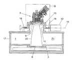
도 1 내지 도 3은 기판(S)의 표면을 처리하는 장치를 도시하고 있다. 장치는 특히 PECVD를 실행하도록 배치된다. 장치는 처리채임버(1)와 기판홀더(2)를 구비하되, 처리될 기판(S)은 기판홀더 상으로 배치된다. 처리채임버(1) 위로 그리고 처리될 기판표면의 반대쪽으로 플라즈마 공급원이 장착된다.1 to 3 show an apparatus for treating the surface of the substrate S. As shown in FIG. The apparatus is specifically arranged to perform PECVD. The apparatus comprises a
도 3으로 도시된 바와 같이, 플라즈마 공급원(3)은 캐스케이드 공급원으로 되어 있다. 캐스케이드 공급원은 선행채임버(6)에 위치된 캐소드(4;cathode)와 처리채임버(1)와 직면하고 있는 플라즈마 공급원(3)의 측면 상으로 위치된 아노드(5;anode)를 구비한다. 비교적 협소한 채널(7)을 지나, 선행채임버(6)가 처리채임버(1)로 개방한다. 채널(7)은 상호전기 절연되어 있는 캐스케이드판(8)과 아노드(5)로 경계되어진다. 사용도중에, 처리채임버(1)는 비교적 낮은 압력, 특히 5,000 Pa 보다 낮게 유지되며, 바람직하게는 500 Pa 보다 낮게 유지된다. 캐소드(4)와 아노드(5) 사이에서 플라즈마가 예컨대 불활성 가스 또는 유체의 발화로 생성되어 이들 사이로 위치된다. 플라즈마가 캐스케이드 공급원에서 생성되면, 선행채임버(6)의 압력(P2)은 처리채임버(1)의 압력보다 높다. 압력(P2)은 예컨대 실제로 대기압 및 0.5~0.1 바아(bar)의 범위로 유지할 수 있다. 처리채임버(1)의 압력이 선행채임버(6)의 압력보다 훨씬 낮기 때문에, 비교적 협소한 채널(7)을 지나 길이연장되는 생성될 플라즈마의 부분(20)이 기판표면과 접촉할 수 있는 처리채임버(1)로 뻗는다.As shown in FIG. 3, the
플라즈마 공급원(3)은 기판표면에 대해서 이동가능하게 배치된다. 이러한 목적을 위해서, 플라즈마 공급원(3)은 장치의 상부하우징(16)에 장착된다. 상부하우징(16)은 유연하면서 실제로 기밀을 유지하는 밀봉부로 하부하우징(17)에 연결된다. 바람직한 실시예에서, 밀봉부는 실린더형상의 탄성체(11)로 형성되어 있다. 추가로, 탄성체(11)는 적어도 하나의 플라즈마 공급원(3) 위로 적어도 하나의 상부하우징(16)을 관통하는 탄발력을 가하도록 배치되되, 탄발력의 영향으로 매 시간, 플라즈마 공급원(3)이 다른 위치로 변위될 때 플라즈마 공급원(3)은 도면으로 도시된 시작위치로 이동할 수 있다. 모범적인 본 실시예에서, 탄성체(11)는 박막의 측벽을 갖는 스테인레스강 주름관으로 형성된다.The
플라즈마 공급원(3)을 이동하기 위해서, 상부하우징(16)은 하부하우징(17)에 연결되어 다른 2개의 축(14,15)으로 회전할 수 있다. 이를 위해서, 상부하우징(16)은 베어링 링(19)에 연결되어 회전축(15)으로 회전가능한 반면에, 이 베어링 링(19)이 하부하우징(17)에 장착된 지지부(18)에 연결되어 회전축(14)으로 회전할 수 있다. 장치는 바람직한 위치로 플라즈마 공급원(3)을 갖춘 상부하우징(16)을 이동하기 위해 제1모터(12)와 제2모터(13)를 구비하다. 2개의 회전축(14,15)은 서로 직각방향으로 뻗어 있어, 플라즈마 공급원(3)은 서로 다른 방향으로 이동시킬 수 있다.In order to move the
도 2 및 도 3으로 도시된 바와 같이, 처리채임버(1)는 샤워헤드부(9;showerhead)를 구비한다. 샤워헤드부는 특히 PECVD를 실행하도록 비교적 협소한 채널(7)을 지나 처리채임버(1)로 뻗어 있는 플라즈마(20)에 처리유체를 추가하기 위해 배치된다. 샤워헤드부(9)는 플라즈마(20)가 관통하여 뻗을 수 있는 적어도 하나의 플라즈마 통로(21)를 구비한다. 샤워헤드부는 예컨대 처리유체가 플라즈마(20)로 관통하여 주입될 수 있는 다수의 배출개구부(22)를 구비한다. 샤워헤드부(9)는 적어도 하나의 상부하우징(16)을 매개로 플라즈마 공급원(3)에 연결되되, 샤워헤드부(9)는 플라즈마 공급원(3)의 이동을 실행한다.As shown in Figs. 2 and 3, the
이 장치를 사용하는 도중에, 플라즈마 공급원(3)은 기판표면의 플라즈마처리를 더욱 좋게 하기 위해 이동시킬 수 있다. 예컨대, 기판(S) 상으로 적층될 소재는 균일한 층의 두께를 갖는 장점을 갖는다. 플라즈마 공급원(3)을 갖춘 상부하우징은 예컨대 기판의 가장자리부에 근접하게 소량의 플라즈마를 수용하는 기판표면의 일부가 충분한 처리를 거쳐야 할 초과량의 플라즈마를 수용하도록 이동될 수 있다. 한편, 이와는 반대로 소재는 매우 균일한 방식으로 기판표면에서 드라이에칭될 수 있다. 추가로, 플라즈마 공급원(3)의 이동으로 기판표면의 임의의 부분이 다른 부분보다 상당히 많은 정도의 처리를 수행한다. 예컨대, 기판표면의 절반은 도시된 2개의 회전축(14,15) 중 하나에 대해 공급원을 회전시켜 처리될 수 있는 반면에, 기판표면의 나머지 절반은 실제로 처리되지 않는다.In the course of using this apparatus, the
본 발명은 기술된 모범적인 실시예에 국한되지만은 않는다. 다양한 변형예가 본 발명의 범주 내에서 가능하다.The invention is not limited to the exemplary embodiments described. Various modifications are possible within the scope of the present invention.
예컨대, "처리채임버에 장착된" 적어도 하나의 공급원이라는 용어는 광역적으로 해석될 수 있으며, 예컨대 공급원은 처리채임버의 상단에, 근접하게, 인접하게, 아래에 또는 처리채임버에 대해서 장착되었음을 의미하는 한편, 이 공급원으로 생성된 플라즈마의 적어도 일부는 처리채임버에 배치된 기판(S)의 표면에 도달할 수 있다.For example, the term "at least one source" mounted on a process chamber may be interpreted globally, for example, the source may be mounted on, close to, adjacent to, below or relative to the process chamber. On the other hand, at least a portion of the plasma generated from this source can reach the surface of the substrate S disposed in the process chamber.
추가로, 처리채임버는 하나의 기판보다 하나 이상의 기판이 위치되도록 배치될 수 있다.In addition, the processing chamber may be arranged such that one or more substrates are positioned rather than one substrate.
처리될 기판은 예컨대 반도체 웨이퍼, 음악, 비디오, 컴퓨터자료의 저장매체로 사용되는 CD 또는 DVD, 태양전지기판, 디스플레이 기판, 반사체, 창문, 차창유리, 코팅된 중합 또는 금속기판, 하우징, 램프하우징, 촉매기판 또는 이와 유사한 제품으로 이루어진다. 기판은 디스크형상, 원형, 다각형 또는 다른 형상으로 되어 있다. 기판은 예컨대 3차원 물체로 이루어져 있다. 처리될 기판의 표면은 예컨대 기판의 내부 및 외부로 이루어져 있다. 추가로, 처리될 기판표면은 예컨대 실제로 1차원, 2차원 또는 3차원 표면, 적어도 부분적으로 오목한 표면, 적어도 부분적으로 볼록한 표면 또는 이상과 유사하거나 상이한 형상의 표면들의 조합으로 이루어진다.Substrates to be treated include, for example, CDs or DVDs used as storage media for semiconductor wafers, music, video and computer materials, solar cell substrates, display substrates, reflectors, windows, windshields, coated polymerized or metal substrates, housings, lamp housings, It consists of a catalyst substrate or similar products. The substrate is in disk, circle, polygon or other shape. The substrate is made of, for example, a three-dimensional object. The surface of the substrate to be treated consists, for example, inside and outside of the substrate. In addition, the substrate surface to be treated consists of, for example, a one-dimensional, two-dimensional or three-dimensional surface, at least partially concave surface, at least partially convex surface or a combination of surfaces similar or different in shape.
PECVD로 적층될 소재는 본 명세서의 범주를 벗어난 다양한 소재로도 이루어지되, 주기율의 원소 및 이들 원자 및 분자의 조합체로 적층될 수 있다. 본 발명은 이동가능한 공급원으로 한정될 뿐만 아니라 이동가능한 처리유체 공급원을 갖춘 고정배치된 공급원으로 이루어질 수 있다. 본 발명은 또한 복합적인 이동가능한 공급원 및 이동가능한 처리유체 공급원을 제공하는 방법 및 장치에 관한 것이다.The material to be deposited by PECVD is also composed of various materials that are outside the scope of the present specification, but may be laminated with elements of the periodicity and combinations of these atoms and molecules. The present invention is not only limited to a movable source but can also consist of a fixedly arranged source with a movable treatment fluid source. The invention also relates to a method and apparatus for providing multiple movable sources and movable processing fluid sources.
추가로, 처리될 기판(S) 및 기판홀더(2)는 예컨대 기판처리하는 동안에 이동되도록 이동가능하게 배치될 수 있다.In addition, the substrate S to be processed and the
추가로, 플라즈마 공급원 및 처리유체 공급원은 연속적으로, 임의의 순간에, 반복적으로, 간헐적으로, 주기적으로 또는 이와 유사하게 이동될 수 있다. 플라즈마 공급원 및 처리유체 공급원의 이동은 예컨대 기판이 처리채임버의 임의의 처리위치에 안착된 후에 시작될 수 있다.In addition, the plasma source and the treatment fluid source can be moved continuously, at any instant, repeatedly, intermittently, periodically or similarly. Movement of the plasma source and the processing fluid source may begin, for example, after the substrate has been seated in any processing position of the processing chamber.
Claims (31)
Translated fromKoreanApplications Claiming Priority (2)
| Application Number | Priority Date | Filing Date | Title |
|---|---|---|---|
| NL1022155ANL1022155C2 (en) | 2002-12-12 | 2002-12-12 | Method and device for treating a surface of at least one substrate. |
| NL1022155 | 2002-12-12 |
Publications (2)
| Publication Number | Publication Date |
|---|---|
| KR20050100599A KR20050100599A (en) | 2005-10-19 |
| KR100895913B1true KR100895913B1 (en) | 2009-05-07 |
Family
ID=32501543
Family Applications (1)
| Application Number | Title | Priority Date | Filing Date |
|---|---|---|---|
| KR1020057010737AExpired - Fee RelatedKR100895913B1 (en) | 2002-12-12 | 2003-12-12 | Method and apparatus for treating a surface of at least one substrate |
Country Status (11)
| Country | Link |
|---|---|
| US (1) | US7645495B2 (en) |
| EP (1) | EP1604049B1 (en) |
| JP (1) | JP4578979B2 (en) |
| KR (1) | KR100895913B1 (en) |
| CN (1) | CN100489155C (en) |
| AT (1) | ATE358192T1 (en) |
| AU (1) | AU2003296050A1 (en) |
| DE (1) | DE60312902T2 (en) |
| ES (1) | ES2283848T3 (en) |
| NL (1) | NL1022155C2 (en) |
| WO (1) | WO2004053190A1 (en) |
Families Citing this family (53)
| Publication number | Priority date | Publication date | Assignee | Title |
|---|---|---|---|---|
| EP1716727A1 (en)* | 2004-02-20 | 2006-11-02 | The University Of Sydney | An apparatus for plasma treatment |
| US9508886B2 (en) | 2007-10-06 | 2016-11-29 | Solexel, Inc. | Method for making a crystalline silicon solar cell substrate utilizing flat top laser beam |
| US8399331B2 (en) | 2007-10-06 | 2013-03-19 | Solexel | Laser processing for high-efficiency thin crystalline silicon solar cell fabrication |
| US8420435B2 (en) | 2009-05-05 | 2013-04-16 | Solexel, Inc. | Ion implantation fabrication process for thin-film crystalline silicon solar cells |
| US20090107545A1 (en) | 2006-10-09 | 2009-04-30 | Soltaix, Inc. | Template for pyramidal three-dimensional thin-film solar cell manufacturing and methods of use |
| NL1030896C2 (en)* | 2006-01-11 | 2007-07-12 | Otb Group Bv | Method and device for the controlled depositing of material by means of plasma on a three-dimensional substrate. |
| RU2435874C2 (en)* | 2006-04-14 | 2011-12-10 | СИЛИКА ТЕК, ЭлЭлСи | Installation for plasma sedimentation and procedure for manufacture of solar cells |
| US20080210290A1 (en)* | 2006-04-14 | 2008-09-04 | Dau Wu | Plasma inside vapor deposition apparatus and method for making multi-junction silicon thin film solar cell modules and panels |
| WO2008007944A1 (en)* | 2006-07-12 | 2008-01-17 | Technische Universiteit Eindhoven | Method and device for treating a substrate by means of a plasma |
| US8035028B2 (en)* | 2006-10-09 | 2011-10-11 | Solexel, Inc. | Pyramidal three-dimensional thin-film solar cells |
| US7999174B2 (en)* | 2006-10-09 | 2011-08-16 | Solexel, Inc. | Solar module structures and assembly methods for three-dimensional thin-film solar cells |
| US8293558B2 (en)* | 2006-10-09 | 2012-10-23 | Solexel, Inc. | Method for releasing a thin-film substrate |
| US8193076B2 (en) | 2006-10-09 | 2012-06-05 | Solexel, Inc. | Method for releasing a thin semiconductor substrate from a reusable template |
| US20100304521A1 (en)* | 2006-10-09 | 2010-12-02 | Solexel, Inc. | Shadow Mask Methods For Manufacturing Three-Dimensional Thin-Film Solar Cells |
| US20080264477A1 (en)* | 2006-10-09 | 2008-10-30 | Soltaix, Inc. | Methods for manufacturing three-dimensional thin-film solar cells |
| USH2207H1 (en)* | 2007-01-05 | 2007-12-04 | Bijker Martin D | Additional post-glass-removal processes for enhanced cell efficiency in the production of solar cells |
| WO2009026240A1 (en)* | 2007-08-17 | 2009-02-26 | Solexel, Inc. | Methods for liquid transfer coating of three-dimensional substrates |
| US8039052B2 (en)* | 2007-09-06 | 2011-10-18 | Intermolecular, Inc. | Multi-region processing system and heads |
| US20100144080A1 (en)* | 2008-06-02 | 2010-06-10 | Solexel, Inc. | Method and apparatus to transfer coat uneven surface |
| US20100148319A1 (en)* | 2008-11-13 | 2010-06-17 | Solexel, Inc. | Substrates for High-Efficiency Thin-Film Solar Cells Based on Crystalline Templates |
| US8288195B2 (en)* | 2008-11-13 | 2012-10-16 | Solexel, Inc. | Method for fabricating a three-dimensional thin-film semiconductor substrate from a template |
| MY160251A (en)* | 2008-11-26 | 2017-02-28 | Solexel Inc | Truncated pyramid -structures for see-through solar cells |
| US9076642B2 (en) | 2009-01-15 | 2015-07-07 | Solexel, Inc. | High-Throughput batch porous silicon manufacturing equipment design and processing methods |
| US8906218B2 (en) | 2010-05-05 | 2014-12-09 | Solexel, Inc. | Apparatus and methods for uniformly forming porous semiconductor on a substrate |
| US8926803B2 (en)* | 2009-01-15 | 2015-01-06 | Solexel, Inc. | Porous silicon electro-etching system and method |
| MY162405A (en)* | 2009-02-06 | 2017-06-15 | Solexel Inc | Trench Formation Method For Releasing A Thin-Film Substrate From A Reusable Semiconductor Template |
| US8828517B2 (en) | 2009-03-23 | 2014-09-09 | Solexel, Inc. | Structure and method for improving solar cell efficiency and mechanical strength |
| WO2010120850A1 (en)* | 2009-04-14 | 2010-10-21 | Solexel, Inc. | High efficiency epitaxial chemical vapor deposition (cvd) reactor |
| US9099584B2 (en)* | 2009-04-24 | 2015-08-04 | Solexel, Inc. | Integrated three-dimensional and planar metallization structure for thin film solar cells |
| MY165969A (en) | 2009-05-05 | 2018-05-18 | Solexel Inc | High-productivity porous semiconductor manufacturing equipment |
| US9318644B2 (en) | 2009-05-05 | 2016-04-19 | Solexel, Inc. | Ion implantation and annealing for thin film crystalline solar cells |
| US8445314B2 (en)* | 2009-05-22 | 2013-05-21 | Solexel, Inc. | Method of creating reusable template for detachable thin film substrate |
| WO2010138976A1 (en)* | 2009-05-29 | 2010-12-02 | Solexel, Inc. | Three-dimensional thin-film semiconductor substrate with through-holes and methods of manufacturing |
| NL2002980C2 (en)* | 2009-06-05 | 2010-12-07 | Otb Solar Bv | Method for passivating al least a part of a substrate surface. |
| US9111729B2 (en)* | 2009-12-03 | 2015-08-18 | Lam Research Corporation | Small plasma chamber systems and methods |
| CN102763226B (en) | 2009-12-09 | 2016-01-27 | 速力斯公司 | Use high-efficiency photovoltaic back of the body contact solar cell structure and the manufacture method of thin plate semiconductor |
| US8241940B2 (en) | 2010-02-12 | 2012-08-14 | Solexel, Inc. | Double-sided reusable template for fabrication of semiconductor substrates for photovoltaic cell and microelectronics device manufacturing |
| US9190289B2 (en) | 2010-02-26 | 2015-11-17 | Lam Research Corporation | System, method and apparatus for plasma etch having independent control of ion generation and dissociation of process gas |
| KR20130051013A (en) | 2010-06-09 | 2013-05-16 | 솔렉셀, 인크. | High productivity thin film deposition method and system |
| EP2601687A4 (en) | 2010-08-05 | 2018-03-07 | Solexel, Inc. | Backplane reinforcement and interconnects for solar cells |
| US9155181B2 (en) | 2010-08-06 | 2015-10-06 | Lam Research Corporation | Distributed multi-zone plasma source systems, methods and apparatus |
| US9449793B2 (en) | 2010-08-06 | 2016-09-20 | Lam Research Corporation | Systems, methods and apparatus for choked flow element extraction |
| US8999104B2 (en) | 2010-08-06 | 2015-04-07 | Lam Research Corporation | Systems, methods and apparatus for separate plasma source control |
| US9967965B2 (en) | 2010-08-06 | 2018-05-08 | Lam Research Corporation | Distributed, concentric multi-zone plasma source systems, methods and apparatus |
| CN102534568B (en)* | 2010-12-30 | 2014-12-17 | 北京北方微电子基地设备工艺研究中心有限责任公司 | Plasma-enhanced chemical vapor deposition equipment |
| US9748414B2 (en) | 2011-05-20 | 2017-08-29 | Arthur R. Zingher | Self-activated front surface bias for a solar cell |
| CN102796993B (en)* | 2011-05-27 | 2014-05-28 | 北京北方微电子基地设备工艺研究中心有限责任公司 | CVD (Chemical Vapor Deposition) equipment and control method thereof |
| US9177762B2 (en) | 2011-11-16 | 2015-11-03 | Lam Research Corporation | System, method and apparatus of a wedge-shaped parallel plate plasma reactor for substrate processing |
| US10283325B2 (en) | 2012-10-10 | 2019-05-07 | Lam Research Corporation | Distributed multi-zone plasma source systems, methods and apparatus |
| US9783889B2 (en)* | 2012-03-26 | 2017-10-10 | Applied Materials, Inc. | Apparatus for variable substrate temperature control |
| US8735210B2 (en)* | 2012-06-28 | 2014-05-27 | International Business Machines Corporation | High efficiency solar cells fabricated by inexpensive PECVD |
| WO2014098905A1 (en)* | 2012-12-21 | 2014-06-26 | Clearedge Power Corporation | Deposition cloud tower with adjustable field |
| JP2015090916A (en)* | 2013-11-06 | 2015-05-11 | 東京エレクトロン株式会社 | Substrate processing apparatus and substrate processing method |
Citations (3)
| Publication number | Priority date | Publication date | Assignee | Title |
|---|---|---|---|---|
| GB2165990A (en) | 1984-10-22 | 1986-04-23 | Alsthom Sa | Electron-beam external butt welding of tubes |
| US5403399A (en)* | 1987-04-03 | 1995-04-04 | Fujitsu Limited | Method and apparatus for vapor deposition of diamond |
| US6490994B1 (en) | 1999-06-22 | 2002-12-10 | Sharp Kabushiki Kaisha | Plasma processing apparatus |
Family Cites Families (13)
| Publication number | Priority date | Publication date | Assignee | Title |
|---|---|---|---|---|
| DE2054538C3 (en)* | 1970-11-05 | 1979-03-22 | Siemens Ag, 1000 Berlin Und 8000 Muenchen | Device for depositing layers of semiconductor material |
| JPS6179774A (en) | 1984-09-28 | 1986-04-23 | Mitsubishi Heavy Ind Ltd | Method for coating inside surface of vessel |
| JPS6428297A (en)* | 1987-04-03 | 1989-01-30 | Fujitsu Ltd | Vapor phase synthesis of diamond |
| GB8713986D0 (en)* | 1987-06-16 | 1987-07-22 | Shell Int Research | Apparatus for plasma surface treating |
| NL8701530A (en)* | 1987-06-30 | 1989-01-16 | Stichting Fund Ond Material | METHOD FOR TREATING SURFACES OF SUBSTRATES USING A PLASMA AND REACTOR FOR CARRYING OUT THAT METHOD |
| JPH06330324A (en)* | 1993-05-17 | 1994-11-29 | Fuji Electric Co Ltd | Dry thin film processing equipment |
| US6051114A (en)* | 1997-06-23 | 2000-04-18 | Applied Materials, Inc. | Use of pulsed-DC wafer bias for filling vias/trenches with metal in HDP physical vapor deposition |
| JP2000109979A (en)* | 1998-10-05 | 2000-04-18 | Tokujiro Okui | Surface treatment method by dc arc discharge plasma |
| US6068201A (en)* | 1998-11-05 | 2000-05-30 | Sulzer Metco (Us) Inc. | Apparatus for moving a thermal spray gun in a figure eight over a substrate |
| US6344416B1 (en)* | 2000-03-10 | 2002-02-05 | International Business Machines Corporation | Deliberate semiconductor film variation to compensate for radial processing differences, determine optimal device characteristics, or produce small productions |
| JP2002118027A (en)* | 2000-10-10 | 2002-04-19 | Anelva Corp | Magnetic film forming device and method therefor |
| US6397776B1 (en)* | 2001-06-11 | 2002-06-04 | General Electric Company | Apparatus for large area chemical vapor deposition using multiple expanding thermal plasma generators |
| WO2003017737A2 (en)* | 2001-08-16 | 2003-02-27 | Dow Global Technologies Inc. | Cascade arc plasma and abrasion resistant coatings made therefrom |
- 2002
- 2002-12-12NLNL1022155Apatent/NL1022155C2/ennot_activeIP Right Cessation
- 2003
- 2003-12-12USUS10/538,652patent/US7645495B2/ennot_activeExpired - Fee Related
- 2003-12-12WOPCT/NL2003/000886patent/WO2004053190A1/enactiveIP Right Grant
- 2003-12-12KRKR1020057010737Apatent/KR100895913B1/ennot_activeExpired - Fee Related
- 2003-12-12DEDE60312902Tpatent/DE60312902T2/ennot_activeExpired - Lifetime
- 2003-12-12ESES03782978Tpatent/ES2283848T3/ennot_activeExpired - Lifetime
- 2003-12-12AUAU2003296050Apatent/AU2003296050A1/ennot_activeAbandoned
- 2003-12-12CNCNB2003801086599Apatent/CN100489155C/ennot_activeExpired - Fee Related
- 2003-12-12JPJP2004558567Apatent/JP4578979B2/ennot_activeExpired - Fee Related
- 2003-12-12EPEP03782978Apatent/EP1604049B1/ennot_activeExpired - Lifetime
- 2003-12-12ATAT03782978Tpatent/ATE358192T1/ennot_activeIP Right Cessation
Patent Citations (3)
| Publication number | Priority date | Publication date | Assignee | Title |
|---|---|---|---|---|
| GB2165990A (en) | 1984-10-22 | 1986-04-23 | Alsthom Sa | Electron-beam external butt welding of tubes |
| US5403399A (en)* | 1987-04-03 | 1995-04-04 | Fujitsu Limited | Method and apparatus for vapor deposition of diamond |
| US6490994B1 (en) | 1999-06-22 | 2002-12-10 | Sharp Kabushiki Kaisha | Plasma processing apparatus |
Non-Patent Citations (1)
| Title |
|---|
| BUURON A J M ET AL: "FAST DEPOSITION OF AMORPHOUS HYDROGENATED CARBON AND SILICON LAYERS" APPLIED POLYMER SYMPOSIA, JOHN WILEY AND SONS,INC. NEW YORK, US, vol. 54, 1994, pages 115-121, XP000468649 ISS |
Also Published As
| Publication number | Publication date |
|---|---|
| US20060231031A1 (en) | 2006-10-19 |
| CN100489155C (en) | 2009-05-20 |
| KR20050100599A (en) | 2005-10-19 |
| AU2003296050A1 (en) | 2004-06-30 |
| NL1022155C2 (en) | 2004-06-22 |
| EP1604049B1 (en) | 2007-03-28 |
| US7645495B2 (en) | 2010-01-12 |
| CN1738923A (en) | 2006-02-22 |
| ATE358192T1 (en) | 2007-04-15 |
| DE60312902D1 (en) | 2007-05-10 |
| DE60312902T2 (en) | 2007-12-06 |
| JP4578979B2 (en) | 2010-11-10 |
| EP1604049A1 (en) | 2005-12-14 |
| WO2004053190A1 (en) | 2004-06-24 |
| JP2006509907A (en) | 2006-03-23 |
| ES2283848T3 (en) | 2007-11-01 |
Similar Documents
| Publication | Publication Date | Title |
|---|---|---|
| KR100895913B1 (en) | Method and apparatus for treating a surface of at least one substrate | |
| US5204144A (en) | Method for plasma deposition on apertured substrates | |
| TW201625809A (en) | Film forming method | |
| KR20000062949A (en) | Plasma CVD Film-Forming Device | |
| JP2017112258A (en) | Film deposition method, and film deposition device | |
| CN1235647A (en) | Method and apparatus for depositing carbon-rich coating on moving substate | |
| JPH10321595A (en) | Plasma treatment system | |
| CN108206133B (en) | Particle removing method and substrate processing method | |
| KR102634044B1 (en) | Apparatus for Distributing Gas and Apparatus for Processing Substrate | |
| KR20190133606A (en) | Dry cleaning method of susceptor and substrate processing apparatus | |
| TW201602395A (en) | Substrate Processing Apparatus and Substrate Processing Method | |
| KR20170136280A (en) | Substrate processing apparatus | |
| JP7394694B2 (en) | plasma processing equipment | |
| TW201630071A (en) | Substrate processing apparatus | |
| KR960034479A (en) | METHOD FOR MANUFACTING OXIDE FILM AND METHOD FOR PRODUCING THE SAME | |
| KR102678267B1 (en) | Substrate treatment apparatus and substrate treatment method | |
| KR20230062783A (en) | Method and system for selectively removing material at an edge of a substrate | |
| KR20160146365A (en) | Atomic layer deposition apparatus | |
| JPS6124467B2 (en) | ||
| JPH0978242A (en) | Plasma cvd device | |
| JPS60123033A (en) | Plasma treating device | |
| JP7586599B2 (en) | Film forming apparatus and film forming method | |
| KR20030027505A (en) | Semiconductor processing apparatus having improved exhausting structure | |
| JP2025000255A (en) | Film deposition method and film deposition apparatus | |
| KR20040102600A (en) | Deposition apparatus for manufacturing semiconductor devices |
Legal Events
| Date | Code | Title | Description |
|---|---|---|---|
| E13-X000 | Pre-grant limitation requested | St.27 status event code:A-2-3-E10-E13-lim-X000 | |
| PA0105 | International application | St.27 status event code:A-0-1-A10-A15-nap-PA0105 | |
| T11-X000 | Administrative time limit extension requested | St.27 status event code:U-3-3-T10-T11-oth-X000 | |
| P11-X000 | Amendment of application requested | St.27 status event code:A-2-2-P10-P11-nap-X000 | |
| P13-X000 | Application amended | St.27 status event code:A-2-2-P10-P13-nap-X000 | |
| PG1501 | Laying open of application | St.27 status event code:A-1-1-Q10-Q12-nap-PG1501 | |
| A201 | Request for examination | ||
| PA0201 | Request for examination | St.27 status event code:A-1-2-D10-D11-exm-PA0201 | |
| E902 | Notification of reason for refusal | ||
| PE0902 | Notice of grounds for rejection | St.27 status event code:A-1-2-D10-D21-exm-PE0902 | |
| T11-X000 | Administrative time limit extension requested | St.27 status event code:U-3-3-T10-T11-oth-X000 | |
| T11-X000 | Administrative time limit extension requested | St.27 status event code:U-3-3-T10-T11-oth-X000 | |
| T11-X000 | Administrative time limit extension requested | St.27 status event code:U-3-3-T10-T11-oth-X000 | |
| T11-X000 | Administrative time limit extension requested | St.27 status event code:U-3-3-T10-T11-oth-X000 | |
| T11-X000 | Administrative time limit extension requested | St.27 status event code:U-3-3-T10-T11-oth-X000 | |
| E13-X000 | Pre-grant limitation requested | St.27 status event code:A-2-3-E10-E13-lim-X000 | |
| P11-X000 | Amendment of application requested | St.27 status event code:A-2-2-P10-P11-nap-X000 | |
| P13-X000 | Application amended | St.27 status event code:A-2-2-P10-P13-nap-X000 | |
| E701 | Decision to grant or registration of patent right | ||
| PE0701 | Decision of registration | St.27 status event code:A-1-2-D10-D22-exm-PE0701 | |
| GRNT | Written decision to grant | ||
| PR0701 | Registration of establishment | St.27 status event code:A-2-4-F10-F11-exm-PR0701 | |
| PR1002 | Payment of registration fee | St.27 status event code:A-2-2-U10-U12-oth-PR1002 Fee payment year number:1 | |
| PG1601 | Publication of registration | St.27 status event code:A-4-4-Q10-Q13-nap-PG1601 | |
| PN2301 | Change of applicant | St.27 status event code:A-5-5-R10-R13-asn-PN2301 St.27 status event code:A-5-5-R10-R11-asn-PN2301 | |
| PN2301 | Change of applicant | St.27 status event code:A-5-5-R10-R13-asn-PN2301 St.27 status event code:A-5-5-R10-R11-asn-PN2301 | |
| PN2301 | Change of applicant | St.27 status event code:A-5-5-R10-R11-asn-PN2301 | |
| FPAY | Annual fee payment | Payment date:20120416 Year of fee payment:4 | |
| PR1001 | Payment of annual fee | St.27 status event code:A-4-4-U10-U11-oth-PR1001 Fee payment year number:4 | |
| PN2301 | Change of applicant | St.27 status event code:A-5-5-R10-R13-asn-PN2301 St.27 status event code:A-5-5-R10-R11-asn-PN2301 | |
| LAPS | Lapse due to unpaid annual fee | ||
| PC1903 | Unpaid annual fee | St.27 status event code:A-4-4-U10-U13-oth-PC1903 Not in force date:20130425 Payment event data comment text:Termination Category : DEFAULT_OF_REGISTRATION_FEE | |
| PC1903 | Unpaid annual fee | St.27 status event code:N-4-6-H10-H13-oth-PC1903 Ip right cessation event data comment text:Termination Category : DEFAULT_OF_REGISTRATION_FEE Not in force date:20130425 |