KR100895854B1 - Method of manufacturing flash memory having two control gates - Google Patents
Method of manufacturing flash memory having two control gatesDownload PDFInfo
- Publication number
- KR100895854B1 KR100895854B1KR1020070107807AKR20070107807AKR100895854B1KR 100895854 B1KR100895854 B1KR 100895854B1KR 1020070107807 AKR1020070107807 AKR 1020070107807AKR 20070107807 AKR20070107807 AKR 20070107807AKR 100895854 B1KR100895854 B1KR 100895854B1
- Authority
- KR
- South Korea
- Prior art keywords
- gate
- dielectric layer
- layer
- control gate
- cell transistor
- Prior art date
- Legal status (The legal status is an assumption and is not a legal conclusion. Google has not performed a legal analysis and makes no representation as to the accuracy of the status listed.)
- Active
Links
Images


Classifications
- H—ELECTRICITY
- H10—SEMICONDUCTOR DEVICES; ELECTRIC SOLID-STATE DEVICES NOT OTHERWISE PROVIDED FOR
- H10D—INORGANIC ELECTRIC SEMICONDUCTOR DEVICES
- H10D30/00—Field-effect transistors [FET]
- H10D30/60—Insulated-gate field-effect transistors [IGFET]
- H10D30/68—Floating-gate IGFETs
- H10D30/6891—Floating-gate IGFETs characterised by the shapes, relative sizes or dispositions of the floating gate electrode
- H—ELECTRICITY
- H10—SEMICONDUCTOR DEVICES; ELECTRIC SOLID-STATE DEVICES NOT OTHERWISE PROVIDED FOR
- H10B—ELECTRONIC MEMORY DEVICES
- H10B41/00—Electrically erasable-and-programmable ROM [EEPROM] devices comprising floating gates
- H10B41/10—Electrically erasable-and-programmable ROM [EEPROM] devices comprising floating gates characterised by the top-view layout
- H—ELECTRICITY
- H10—SEMICONDUCTOR DEVICES; ELECTRIC SOLID-STATE DEVICES NOT OTHERWISE PROVIDED FOR
- H10B—ELECTRONIC MEMORY DEVICES
- H10B63/00—Resistance change memory devices, e.g. resistive RAM [ReRAM] devices
- H10B63/30—Resistance change memory devices, e.g. resistive RAM [ReRAM] devices comprising selection components having three or more electrodes, e.g. transistors
- H—ELECTRICITY
- H10—SEMICONDUCTOR DEVICES; ELECTRIC SOLID-STATE DEVICES NOT OTHERWISE PROVIDED FOR
- H10D—INORGANIC ELECTRIC SEMICONDUCTOR DEVICES
- H10D30/00—Field-effect transistors [FET]
- H10D30/01—Manufacture or treatment
- H10D30/021—Manufacture or treatment of FETs having insulated gates [IGFET]
- H10D30/0411—Manufacture or treatment of FETs having insulated gates [IGFET] of FETs having floating gates
- H—ELECTRICITY
- H10—SEMICONDUCTOR DEVICES; ELECTRIC SOLID-STATE DEVICES NOT OTHERWISE PROVIDED FOR
- H10D—INORGANIC ELECTRIC SEMICONDUCTOR DEVICES
- H10D64/00—Electrodes of devices having potential barriers
- H10D64/01—Manufacture or treatment
- H10D64/031—Manufacture or treatment of data-storage electrodes
- H10D64/035—Manufacture or treatment of data-storage electrodes comprising conductor-insulator-conductor-insulator-semiconductor structures
Landscapes
- Non-Volatile Memory (AREA)
- Semiconductor Memories (AREA)
Abstract
Translated fromKoreanDescription
Translated fromKorean본 발명은 플래시 메모리의 구조 및 이를 제조하는 방법에 관한 것으로, 더욱 상세하게는 하나의 메모리 셀에 게이트가 분리된 구조를 가지는 플래시 메모리 및 이를 제조하는 방법에 관한 것이다.The present invention relates to a structure of a flash memory and a method of manufacturing the same, and more particularly, to a flash memory having a structure in which a gate is separated in one memory cell and a method of manufacturing the same.
플래시 메모리는 대표적인 비휘발성 메모리로서 고집적 및 대용량이 가능하다. 특히, 우수한 데이터 보존성을 가지므로, 시스템 내에서 메인 메모리로 대체 가능하며 기존의 하드 디스크를 대체할 수 있는 소자로서 주목을 받고 있다.Flash memory is a representative non-volatile memory that can be integrated and large capacity. In particular, since it has excellent data retention, it can be replaced with a main memory in a system and attracts attention as a device that can replace an existing hard disk.
통상적인 플래시 메모리에서 데이터를 저장하는 양상은 셀 트랜지스터의 문턱전압의 변경에 의해 달성한다. 특히, 상기 셀 트랜지스터는 터널링 유전막, 부유 게이트, 게이트간 유전막 및 제어 게이트로 구성된 게이트 패턴을 가진다. 플래시 메모리에서의 데이터의 프로그래밍과 소거 동작은 파울러-노드하임(Fowler-Nordheim) 터널링 또는 핫 캐리어 주입(hot carrier injection)에 의해 수행된다. 프로그래밍 동작은 기판으로부터 전자를 터널링 유전막을 통해 부유 게이트로 포획시키는 동작이다. 또한, 소거 동작은 부유 게이트에 포획된 전자들을 터널링 유전 막을 통해 기판으로 이동시키는 동작이다. 상술한 동작들이 원활하게 수행되기 위해서는 제어 게이트에 인가되는 전압에 비해 비교적 높은 전압 레벨이 부유 게이트에 인가되어야 한다. 즉, 동일한 전압이 제어 게이트에 인가되더라도 유전막들의 적절한 선택에 의해 높은 레벨의 전압이 부유 게이트에 인가되도록 한다.The aspect of storing data in a conventional flash memory is achieved by changing the threshold voltage of the cell transistor. In particular, the cell transistor has a gate pattern including a tunneling dielectric layer, a floating gate, an inter-gate dielectric layer, and a control gate. Programming and erase operations of data in flash memory are performed by Fowler-Nordheim tunneling or hot carrier injection. The programming operation is the operation of trapping electrons from the substrate through the tunneling dielectric film to the floating gate. In addition, the erase operation is an operation of moving electrons trapped in the floating gate to the substrate through the tunneling dielectric film. In order to perform the above-described operations smoothly, a relatively high voltage level must be applied to the floating gate compared to the voltage applied to the control gate. That is, even if the same voltage is applied to the control gate, a high level of voltage is applied to the floating gate by appropriate selection of the dielectric films.
또한, 부유 게이트에서의 전자의 포획인 프로그래밍 동작과 포획된 전자를 기판으로 이동시키는 소거 동작을 원활하게 수행하기 위해, 부유 게이트를 실리콘 질화막으로 구성하는 구조가 최근에 적용되고 있다. 이를 ONO(oxide/nitride/oxide) 구조라 지칭한다. 즉, 부유 게이트는 질화막으로 구성되고, 하부 및 상부의 유전막들은 산화막으로 구성된다. 산화막으로 구성된 터널링 유전막을 통과한 전자들이 실리콘 질화막 계면에 포획된다. 즉, 다결정 실리콘으로 부유 게이트를 구성하는 경우에는 다결정 실리콘의 벌크 내에 포획됨에 반해 실리콘 질화막 계면에 전자들이 포획되는 ONO 구조에서는 용이하게 전자의 포획 및 기판으로의 소거 동작을 일으킬 수 있는 잇점이 있다.In addition, in order to smoothly perform a programming operation which is the capture of electrons in the floating gate and an erase operation for moving the captured electrons to the substrate, a structure in which the floating gate is made of a silicon nitride film has been recently applied. This is called an ONO (oxide / nitride / oxide) structure. That is, the floating gate is formed of a nitride film, and the lower and upper dielectric films are formed of an oxide film. Electrons passing through the tunneling dielectric film composed of the oxide film are trapped at the silicon nitride film interface. That is, when the floating gate is formed of polycrystalline silicon, the trapped electrons are trapped in the bulk of the polycrystalline silicon, but in the ONO structure in which electrons are trapped at the silicon nitride film interface, the electrons can be easily trapped and erased to the substrate.
도 1은 종래 기술에 따른 플래시 메모리의 셀 트랜지스터를 도시한 단면도이다.1 is a cross-sectional view illustrating a cell transistor of a flash memory according to the prior art.
도 1을 참조하면, 셀 트랜지스터는 ONO 구조를 가진다. 즉, 기판(100) 상에는 소스(110) 및 드레인 영역(120)이 정의되고, 소스 영역(100) 및 드레인 영역(110) 사이의 채널 영역의 상부에는 게이트 패턴(130)이 구비된다.Referring to FIG. 1, the cell transistor has an ONO structure. That is, the
게이트 패턴(130)은 터널링 유전막(132), 부유 게이트(134), 게이트간 유전막(136) 및 제어 게이트(138)로 구성된다. 특히, ONO 구조에서는 상기 터널링 유전 막(132) 및 게이트간 유전막(138)은 산화막으로 구성되며, 부유 게이트(136)는 실리콘 질화막으로 구성된다. 또한, 프로그램 동작시에는 전자는 부유 게이트(136)의 계면에 트랩된다. 소거 동작시에는 부유 게이트(136)의 계면에 트랩된 전자는 터널링 유전막(132)을 통해 기판(100)으로 전달된다.The
프로그램 동작 및 소거 동작에 의해 셀 트랜지스터의 문턱전압은 변경된다. 즉, 셀 트랜지스터에 대한 정보의 저장은 문턱 전압의 변경에 의해 달성된다. 이러한 정보의 저장은 하나의 셀 트랜지스터에 대해 1 비트가 저장되는 것이 일반적이다.The threshold voltage of the cell transistor is changed by the program operation and the erase operation. That is, the storage of information about the cell transistors is achieved by changing the threshold voltage. In the storage of such information, one bit is generally stored for one cell transistor.
그러나, 최근에는 적은 면적에 많은 정보를 저장하여 플래시 메모리의 기억 용량의 효율을 상승시키고자 하는 시도가 진행되고 있다. 특히, 상기 도 1에서 부유 게이트(134)를 2개로 분할하여 2비트의 정보를 저장하고자 하는 시도가 이루어져왔다. 그러나, 2개의 유전막 사이에 개재되는 부유 게이트를 2개로 분할하는 경우, 제조공정이 매우 복잡해지며, 주변 회로의 설계가 용이하지 않다는 문제점이 발생한다. 예컨대, 각각의 셀 트랜지스터들을 스트링 구조로 연결하여 사용하는 낸드형 플래시 메모리에서는 부유 게이트가 상하의 유전막 사이에 개재되는 구성을 취하기가 용이하지 아니하다는 문제점이 노출된다. 또한, 하나의 제어 게이트에 서로 이격된 2개의 부유 게이트들이 구비되는 구성에서는, 각각의 부유 게이트에 트랩되는 전하를 제어하기가 용이하지 않다는 문제점이 발생한다.Recently, however, attempts have been made to increase the efficiency of the storage capacity of a flash memory by storing a lot of information in a small area. In particular, an attempt has been made to store two bits of information by dividing the
본 발명의 제1 목적은 하나의 셀 트랜지스터가 4비트를 저장할 수 있는 플래시 메모리를 제공하는데 있다.It is a first object of the present invention to provide a flash memory in which one cell transistor can store 4 bits.
본 발명의 제2 목적은 상기 제1 목적을 달성하기 위한 플래시 메모리의 제조방법을 제공하는데 있다.A second object of the present invention is to provide a method of manufacturing a flash memory for achieving the first object.
상기 제1 목적을 달성하기 위한 본 발명은, 기판; 상기 기판 상에 형성된 게이트 패턴; 상기 기판의 표면으로부터 형성되고, 상기 게이트 패턴의 측면에 형성된 소스 영역; 및 상기 기판의 표면으로부터 형성되고, 상기 게이트 패턴을 중심으로 상기 소스 영역에 대향하는 드레인 영역을 포함하고, 상기 게이트 패턴은 터널링 유전막, 상기 터널링 산화막 상에 형성된 부유 게이트, 상기 부유 게이트 상에 형성된 게이트간 유전막, 상기 게이트간 유전막 상에 형성된 제1 제어 게이트 및 상기 게이트간 유전막 상에 형성되고 상기 제1 제어 게이트와 이격된 제2 제어 게이트를 포함하는 플래시 메모리를 제공한다.The present invention for achieving the first object, a substrate; A gate pattern formed on the substrate; A source region formed from a surface of the substrate and formed at a side of the gate pattern; And a drain region formed from a surface of the substrate and facing the source region about the gate pattern, wherein the gate pattern includes a tunneling dielectric film, a floating gate formed on the tunneling oxide film, and a gate formed on the floating gate. A flash memory includes an inter dielectric layer, a first control gate formed on the inter-gate dielectric layer, and a second control gate formed on the inter-gate dielectric layer and spaced apart from the first control gate.
상기 제2 목적을 달성하기 위한 본 발명은, 기판 상에 터널링 유전층, 부유 게이트층, 게이트간 유전층 및 제어 게이트층을 순차적으로 형성하는 단계; 상기 기판 상에 제1 영역을 정의하고, 상기 제1 영역의 게이트간 유전층 및 제어 게이트층을 식각하여 상기 부유 게이트층을 노출시키는 단계; 상기 제1 영역의 상기 부유 게이트층이 노출된 표면 및 상기 제어 게이트층 측면에 중간 유전층을 형성하는 단 계; 상기 중간 유전층 상에 상기 중간 게이트층을 형성하는 단계; 및 상기 중간 게이트층 및 상기 제어 게이트층 상부에 영역을 정의하고, 하나의 셀 트랜지스터가 2개의 제어 게이트층을 가지도록 기판 표면이 노출되도록 식각하는 단계를 포함하는 플래시 메모리의 제조 방법을 제공한다.According to another aspect of the present invention, there is provided a method including: sequentially forming a tunneling dielectric layer, a floating gate layer, an inter-gate dielectric layer, and a control gate layer on a substrate; Defining a first region on the substrate and etching the inter-gate dielectric layer and the control gate layer of the first region to expose the floating gate layer; Forming an intermediate dielectric layer on the exposed surface of the first region and on the side of the control gate layer; Forming the intermediate gate layer on the intermediate dielectric layer; And defining a region over the intermediate gate layer and the control gate layer, and etching the substrate surface to expose one cell transistor having two control gate layers.
본 발명에서는 하나의 셀 트랜지스터가 서로 분리된 2개의 제어 게이트들을 가진다. 이를 통하여 하나의 셀 트랜지스터는 4 비트의 데이터를 저장할 수 있으며, 4 비트의 데이터에 대한 읽기 동작은 2회에 걸쳐서 수행된다. 따라서, 동일한 셀 면적을 가지면서 더욱 많은 정보를 하나의 셀에 저장할 수 있으며, 더욱 빠른 읽기 동작을 수행할 수 있다.In the present invention, one cell transistor has two control gates separated from each other. As a result, one cell transistor can store 4 bits of data, and the read operation of the 4 bits of data is performed twice. Therefore, more information can be stored in one cell while having the same cell area, and a faster read operation can be performed.
본 발명은 다양한 변경을 가할 수 있고 여러 가지 형태를 가질 수 있는 바, 특정 실시예들을 도면에 예시하고 본문에 상세하게 설명하고자 한다. 그러나, 이는 본 발명을 특정한 개시 형태에 대해 한정하려는 것이 아니며, 본 발명의 사상 및 기술 범위에 포함되는 모든 변경, 균등물 내지 대체물을 포함하는 것으로 이해되어야 한다. 각 도면을 설명하면서 유사한 참조부호를 유사한 구성요소에 대해 사용하였다.As the inventive concept allows for various changes and numerous embodiments, particular embodiments will be illustrated in the drawings and described in detail in the text. However, this is not intended to limit the present invention to the specific disclosed form, it should be understood to include all modifications, equivalents, and substitutes included in the spirit and scope of the present invention. In describing the drawings, similar reference numerals are used for similar elements.
어떤 구성요소가 다른 구성요소의 "상부" 있다거나 "하부" 있다고 언급된 때에는, 그 다른 구성요소에 직접적으로 형성되어 있을 수도 있지만, 중간에 다른 구성요소가 존재할 수도 있다고 이해되어야 할 것이다.When a component is referred to as being "top" or "bottom" of another component, it should be understood that other components may be present in between, although they may be formed directly on the other component.
본 출원에서 사용한 용어는 단지 특정한 실시예를 설명하기 위해 사용된 것으로, 본 발명을 한정하려는 의도가 아니다. 단수의 표현은 문맥상 명백하게 다르게 뜻하지 않는 한, 복수의 표현을 포함한다. 본 출원에서, "포함하다" 또는 "가지다" 등의 용어는 명세서상에 기재된 특징, 숫자, 단계, 동작, 구성요소, 부분품 또는 이들을 조합한 것이 존재함을 지정하려는 것이지, 하나 또는 그 이상의 다른 특징들이나 숫자, 단계, 동작, 구성요소, 부분품 또는 이들을 조합한 것들의 존재 또는 부가 가능성을 미리 배제하지 않는 것으로 이해되어야 한다.The terminology used herein is for the purpose of describing particular example embodiments only and is not intended to be limiting of the present invention. Singular expressions include plural expressions unless the context clearly indicates otherwise. In this application, the terms "comprise" or "have" are intended to indicate that there is a feature, number, step, action, component, part, or combination thereof described in the specification, and one or more other features. It is to be understood that the present invention does not exclude the possibility of the presence or the addition of numbers, steps, operations, components, parts, or combinations thereof.
다르게 정의되지 않는 한, 기술적이거나 과학적인 용어를 포함해서 여기서 사용되는 모든 용어들은 본 발명이 속하는 기술 분야에서 통상의 지식을 가진 자에 의해 일반적으로 이해되는 것과 동일한 의미를 가지고 있다. 일반적으로 사용되는 사전에 정의되어 있는 것과 같은 용어들은 관련 기술의 문맥 상 가지는 의미와 일치하는 의미를 가지는 것으로 해석되어야 하며, 본 출원에서 명백하게 정의하지 않는 한, 이상적이거나 과도하게 형식적인 의미로 해석되지 않는다.Unless defined otherwise, all terms used herein, including technical or scientific terms, have the same meaning as commonly understood by one of ordinary skill in the art. Terms such as those defined in the commonly used dictionaries should be construed as having meanings consistent with the meanings in the context of the related art and shall not be construed in ideal or excessively formal meanings unless expressly defined in this application. Do not.
이하, 첨부한 도면들을 참조하여, 본 발명의 바람직한 실시예를 보다 상세하게 설명하고자 한다.Hereinafter, with reference to the accompanying drawings, it will be described in detail a preferred embodiment of the present invention.
도 2는 본 발명의 실시예에 따른 플래시 메모리의 셀 트랜지스터를 도시한 단면도이다.2 is a cross-sectional view illustrating a cell transistor of a flash memory according to an embodiment of the present invention.
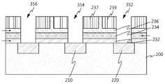
도 2를 참조하면, 본 실시예에 따른 셀 트랜지스터는 기판(200) 상에 형성된 소스 영역(210), 드레인 영역(220) 및 게이트 패턴(230)으로 구성된다.Referring to FIG. 2, the cell transistor according to the present exemplary embodiment includes a
상기 게이트 패턴(230)은 터널링 유전막(232), 부유 게이트(234), 게이트간 유전막(236), 제1 제어 게이트(237) 및 제2 제어 게이트(239)로 구성된다.The
상기 터널링 유전막(232)은 실리콘 산화막으로 구성됨이 바람직하다. 따라서, 상기 터널링 유전막(232)은 열산화 공정을 이용하여 형성될 수 있다. 이외에도 상기 터널링 유전막(232)은 원자층 증착 또는 화학 기상 증착을 통해 형성될 수도 있다. 터널링 유전막(232)이 열산화 공정을 통해 형성되는 경우, 챔버 내에 수소 및 산소를 주입하여 소정의 압력과 온도 조건에서 기판의 실리콘을 산화시켜서 실리콘 산화막을 형성할 수 있다.The tunneling
상기 터널링 유전막(232) 상부에는 부유 게이트(234)가 구비된다. 상기 부유 게이트(234)는 실리콘 질화물로 구성된다.The
상기 부유 게이트(234)의 상부에는 게이트간 유전막(236)이 구비된다. 상기 게이트간 유전막(236)은 실리콘 산화물 또는 금속 산화물로 구성된다. 특히, 금속 산화물은 고유전율을 실현하기 위해 하프늄 산화물, 티타늄 산화물, 이트륨 산화물, 알루미늄 산화물, 탄탈륨 산화물 및 지르코늄 산화물로 구성된 그룹에서 선택된 어느 하나일 수 있으며, 이들 그룹에서 선택된 하나에 질소 또는 실리콘이 첨가될 수도 있으며, 이들의 복합막일 수도 있다.An inter-gate
상기 게이트간 유전막(236)의 상부에는 제1 제어 게이트(237) 및 제2 제어 게이트(239)가 구비된다. 또한, 제1 제어 게이트(237) 및 제2 제어 게이트(239)는 서로 이격된 상태로 배치되며, 이들 사이의 이격공간은 게이트간 유전막(236)으로 매립된다.The
제1 제어 게이트(237) 및 제2 제어 게이트(239)로는 다결정 실리콘, 금속, 도전성 금속질화물 또는 도전성 산화물 사용될 수 있다. 바람직하게는 상기 제1 제어 게이트(237) 및 제2 제어 게이트(239)는 다결정 실리콘으로 형성한다.As the
또한, 상기 도 2에서는 도시되지 아니하였으나, 게이트 패턴(230)의 측면에는 질화물로 구성된 측벽 스페이서가 더 구비될 수 있다.In addition, although not shown in FIG. 2, a sidewall spacer made of nitride may be further provided on a side surface of the
상기 도 2에서, 제1 제어 게이트(237)에 프로그램 전압이 인가되는 시간에 따라, 셀 트랜지스터에는 2 비트의 데이터가 프로그램될 수 있다. 또한, 제2 제어 게이트(239)에 프로그램 전압이 인가되는 시간에 따라서도 2 비트의 데이터가 프로그램될 수 있다.In FIG. 2, two bits of data may be programmed in a cell transistor according to a time when a program voltage is applied to the
따라서, 제1 제어 게이트(237)를 통해 프로그램된 데이터를 상위 비트로 설정하고, 제2 제어 게이트(239)를 통해 프로그램된 데이터를 하위 비트로 설정하는 경우, 하나의 셀 트랜지스터는 4 비트의 데이터를 저장할 수 있다.Therefore, when the data programmed through the
도 3a 내지 도 3d는 본 발명의 바람직한 실시예에 따라 상기 도 2에 도시된 플래시 메모리의 셀 트랜지스터를 형성하는 방법을 도시한 단면도들이다.3A to 3D are cross-sectional views illustrating a method of forming a cell transistor of the flash memory shown in FIG. 2 according to a preferred embodiment of the present invention.
도 3a를 참조하면, 기판(200) 상에 터널링 유전층(310), 부유 게이트층(320), 게이트간 유전층(330) 및 제어 게이트층(240)을 순차적으로 형성한다.Referring to FIG. 3A, the
기판(200)은 p형임이 바람직하다. 이는 이후에 형성되는 소스 영역 및 드레인 영역이 n+로 도핑되는 상황을 대비하기 위한 것이다.The
p형 기판(200) 상에 터널링 유전층(310)은 화학적 기상증착, 원자층 증착 또는 열산화 공정을 이용하여 형성하되, 열산화 공정을 이용하여 형성함이 바람직하다. 즉, 상기 열산화 공정은 챔버 내에서 수소와 산소를 공급하여 기판을 형성하는 실리콘을 산화시키는 공정이다. 열산화 공정에 의해 형성된 터널링 유전층(310)을 실리콘 산화물로 구성된다.The
계속해서, 터널링 유전층(310) 상에 부유 게이트층(320)을 형성한다. 상기 부유 게이트층(320)은 실리콘 질화물로 구성된다.Subsequently, the floating
또한, 부유 게이트층(320) 상부에는 게이트간 유전층(330)이 형성된다. 상기 게이트간 유전층(330)은 실리콘 산화물 또는 금속 산화물로 구성된다. 만일, 금속 산화물을 이용하는 경우, 상기 금속 산화물은 하프늄 산화물, 티타늄 산화물, 이트륨 산화물, 알루미늄 산화물, 탄탈륨 산화물 및 지르코늄 산화물로 구성된 그룹에서 선택된 어느 하나일 수 있으며, 이들 그룹에서 선택된 하나에 질소 또는 실리콘이 첨가될 수도 있으며, 이들의 복합막일 수도 있다. 이러한 금속 산화물은 게이트간 유전층(330)이 높은 유전상수를 가지도록 한다.In addition, an inter-gate
또한, 게이트간 유전층(330) 상부에는 제어 게이트층(340)이 구비된다. 상기 제어 게이트층(340)은 다결정 실리콘, 금속, 도전성 금속질화물 또는 도전성 산화물로 구성될 수 있다. 바람직하게는 상기 제어 게이트층(340)은 다결정 실리콘으로 형성한다.In addition, a
도 3b를 참조하면, 제어 게이트층(340)이 형성된 기판(200)의 상부 전면에 포토레지스트(미도시)를 도포하고, 통상의 포토리소그래피 공정을 이용하여 제1 영역(350)의 상부를 오픈하는 포토레지스트 패턴을 형성한다. 이어서, 포토레지스트 패턴을 식각 마스트로 하여 오픈된 제1 영역(350)의 상부에 대해 식각 공정을 수행한다. 상기 식각 공정은 이방성 건식 식각임이 바람직하다. 또한, 식각시의 에천트 는 부유 게이트층(320)을 구성하는 물질과 게이트간 유전층(330)을 구성하는 물질과의 식각 선택비를 가지는 물질이라면 어느 것이나 가능하다. 따라서, 식각에 의해 제1 영역(350)에서 부유 게이트층(320)은 노출된다.Referring to FIG. 3B, a photoresist (not shown) is coated on the entire upper surface of the
도 3c를 참조하면, 상기 도 3b에 도시된 제1 영역(350)에서 노출된 부유 게이트층(320) 상부 및 양 측면의 제어 게이트층(340) 상부에 중간 유전층(360)을 도포한다. 상기 중간 유전층(360)은 기 형성된 게이트간 유전층(330)과 동일 물질임이 바람직하다. 계속해서 제어 게이트층(340) 상부에 도포된 중간 유전층을 제거한다. 상기 중간 유전층의 제거는 화학적 기계적 연마에 의해 수행된다. 제어 게이트층(340) 상부에 형성된 게이트간 유전층의 제거에 의해 제1 영역(350)의 부유 게이트층(320) 상부 및 제어 게이트층(340)의 양 측벽에만 중간 유전층(360)이 잔류하게 된다.Referring to FIG. 3C, an
이어서, 중간 유전층(360)이 잔류하는 오픈된 제1 영역(350)을 매립하는 중간 게이트층(370)을 형성한다. 상기 중간 게이트층(370)은 인접한 제어 게이트층(340)과 동일 물질로 형성된다.An
도 3d를 참조하면, 상기 도 3c에 도시된 중간 게이트층(370) 및 제어 게이트층(340) 상부에 포토레지스트(미도시)를 포토하고, 통상의 포토레지스트 공정을 이용하여 제2 영역(352), 제3 영역(354) 및 제4 영역(356)을 정의할 수 있는 포토레지스트 패턴(미도시)을 형성한다.Referring to FIG. 3D, a photoresist (not shown) is photographed on the
이어서, 형성된 포토레지스트 패턴을 식각 마스크로 하여 식각 공정을 수행한다. 상기 식각 공정은 이방성 건식 식각임이 바람직하다. 또한, 상기 식각은 각 각의 제2 영역(352) 내지 제4 영역(356)의 하부에 위치한 기판(200)의 표면이 노출되도록 수행된다. 따라서, 기판(200)의 표면이 드러나는 제2 영역(352) 내지 제4 영역(356)이 오픈된다. 또한 식각을 통해, 각각의 셀 트랜지스터의 터널링 유전막(232), 부유 게이트(234), 게이트간 유전막(236), 제1 제어 게이트(237) 및 제2 제어 게이트(239)가 형성된다. 또한, 제1 제어 게이트(237) 및 제2 제어 게이트(239)는 서로 소정의 거리로 이격되며, 이격 공간에는 게이트간 유전막(236)이 개재된다.Subsequently, an etching process is performed using the formed photoresist pattern as an etching mask. The etching process is preferably anisotropic dry etching. In addition, the etching is performed such that the surface of the
또한, 도면에 미도시되었으나, 각각의 셀 트랜지스터의 게이트 패턴의 측벽을 감싸는 측벽 스페이서를 형성할 수 있다. 이어서, 셀 트랜지스터가 형성된 기판에 대해 이온 주입 공정을 수행하여 소스 영역(210) 및 드레인 영역(220)을 형성한다.In addition, although not shown in the drawing, sidewall spacers surrounding the sidewalls of the gate patterns of the respective cell transistors may be formed. Subsequently, an ion implantation process is performed on the substrate on which the cell transistor is formed to form the
상술한 과정을 통해 다수의 셀 트랜지스터가 형성된다.Through the above-described process, a plurality of cell transistors are formed.
도 4는 본 발명의 바람직한 실시예에 따라 상기 도 1에 도시된 셀 트랜지스터를 이용하여 구성한 낸드형 플래시 메모리의 평면도이다.4 is a plan view of a NAND flash memory constructed using the cell transistor shown in FIG. 1 according to a preferred embodiment of the present invention.
도 4를 참조하면, 정의된 활성영역(400) 주변으로는 활성 영역(400) 사이를 절연하기 위한 얕은 소자 분리막(410)이 존재한다. 또한, 활성영역(400)에는 다수의 셀 트랜지스터들이 구비되며, 셀 트랜지스터 각각에는 2개의 제어 게이트 역할을 수행하는 다수의 워드 라인들 WL00H, WL00L,..., WL31H, WL31L이 구비된다. 상기 도 4에서는 설명의 편의를 위해 각각의 셀 트랜지스터를 구성하는 2개의 워드 라인들 이외의 구성요소는 삭제하였다. 셀 트랜지스터에 구비되는 2개의 워드 라인 들은 각각 상기 도 2에 도시된 제1 제어 게이트 및 제2 제어 게이트에 해당한다.Referring to FIG. 4, a shallow
상기 도 4에서 제1 워드라인은 제1 최상위 워드라인 WL00H 및 제1 최하위 워드라인 WL00L로 구성된다. 이러한 워드라인은 제32 최상위 워드라인 WL31H 및 제32 최상위 워드라인 WL31L까지 순서에 따라 배치된다. 각각의 워드라인들 WL00H, WL00L,..., WL31H, WL31L은 서로 평행하게 배열된 액티브 영역들(400)을 가로지르며 형성된다.In FIG. 4, the first word line includes a first highest word line WL00H and a first lowest word line WL00L. These word lines are arranged in order up to the thirty-second most significant word line WL31H and the thirty-second most significant word line WL31L. Each of the word lines WL00H, WL00L, ..., WL31H, WL31L is formed across the
또한, 제1 워드라인 WL00H, WL00L 상부에는 드레인 선택 라인 DSL이 구비된다. 상기 도 4에 미도시되었으나, 상기 드레인 선택 라인 DSL은 드레인 선택 트랜지스터의 온/오프 동작을 제어한다.In addition, a drain select line DSL is provided on the first word lines WL00H and WL00L. Although not shown in FIG. 4, the drain select line DSL controls on / off operation of the drain select transistor.
또한, 워드라인의 마지막 순번인 제32 워드라인 WL31H, WL31L의 하부에는 소스 선택 라인 SSL이 구비된다. 도 4에 미도시되었으나, 상기 소스 선택 라인 SSL은 소스 선택 트랜지스터의 온/오프 동작을 제어한다.In addition, a source select line SSL is provided under the 32nd word lines WL31H and WL31L, which are the last order of the word lines. Although not shown in FIG. 4, the source select line SSL controls on / off operation of the source select transistor.
상술한 낸드형 플래시 메모리의 구조는 하나의 셀 트랜지스터가 2개의 제어 게이트들에 해당하는 최상위 워드라인 및 최하위 워드라인에 의해 제어된다.The structure of the NAND flash memory described above is controlled by the highest word line and the lowest word line in which one cell transistor corresponds to two control gates.
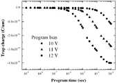
도 5는 본 발명의 바람직한 실시예에 따라 상기 도 2에 도시된 셀 트랜지스터에서 프로그램 시간에 따라 부유 게이트에 트랩되는 전하량을 도시한 그래프이다.5 is a graph showing the amount of charge trapped in the floating gate according to a program time in the cell transistor shown in FIG. 2 according to a preferred embodiment of the present invention.
상기 도 5에서 나타나는 그래프는 상기 도 2에 도시된 셀 트랜지스터에서, 게이트 구조물의 물성과 두께를 특정의 조건으로 설정하여 획득한 것이다. 즉, 터널링 유전막은 실리콘 산화물로서 5nm의 두께를 가지며, 부유 게이트는 실리콘 질 화물로 구성되고 4nm의 두께를 가진다. 또한, 게이트간 유전막은 실리콘 산화물로서 8nm의 두께를 가지며, 제1 제어 게이트 및 제2 제어 게이트는 다결정 실리콘으로 구성되고, 50nm의 두께를 가지도록 설정하였다.The graph shown in FIG. 5 is obtained by setting the physical properties and the thickness of the gate structure in a specific condition in the cell transistor shown in FIG. 2. That is, the tunneling dielectric film has a thickness of 5 nm as the silicon oxide, the floating gate is composed of silicon nitride and has a thickness of 4 nm. The inter-gate dielectric film has a thickness of 8 nm as the silicon oxide, and the first control gate and the second control gate are made of polycrystalline silicon and set to have a thickness of 50 nm.
도 5를 참조하면, 2개의 제어 게이트들 중에서 특정의 하나의 제어 게이트를 선택하여 프로그램 전압을 인가한다. 시간이 증가할수록 부유 게이트의 계면에 트랩되는 전자의 양은 증가한다. 또한, 선택된 하나의 제어 게이트에 인가되는 프로그램 전압이 증가할수록 빠른 시간 내에 전자들이 부유 게이트의 계면에 트랩됨을 알 수 있다.Referring to FIG. 5, a specific one of the two control gates is selected to apply a program voltage. As time increases, the amount of electrons trapped at the interface of the floating gate increases. In addition, it can be seen that as the program voltage applied to the selected control gate increases, electrons are trapped at the interface of the floating gate in a short time.
만일, 프로그램 전압을 일정하게 하고, 프로그램 시간을 조절하는 경우, 하나의 게이트를 통해 다수의 상태를 세팅할 수 있다. 본 발명에서는 하나의 게이트에 인가되는 프로그램 시간의 제어에 의해 4개의 상태를 구현할 수 있다. 즉, 매우 짧은 시간 동안, 프로그램 동작을 수행하거나, 프로그램 동작을 수행하지 않고 소거 상태를 유지하여 부유 게이트의 계면에 전자가 없거나 미미하게 존재하는 상태 ‘11’, 부유 게이트의 계면에 제1 전하량이 트랩되는 상태 ‘10’, 부유 게이트의 계면에 제1 전하량보다 많은 제2 전하량이 트랩되는 상태 ‘01’, 충분한 프로그램 시간을 통해 부유 게이트의 계면에 제2 전하량보다 많은 제3 전하량이 트랩되는 상태 ‘00’로 4개의 상태를 세팅할 수 있다.If the program voltage is made constant and the program time is adjusted, multiple states can be set through one gate. In the present invention, four states can be implemented by controlling the program time applied to one gate. That is, for a very short time, a state of '11' in which no electron is present at the interface of the floating gate due to the program operation or the erase operation without maintaining the program operation is present. The trapped state '10', the state in which the second charge amount is trapped more than the first charge amount at the interface of the floating gate, and the trapped third amount of the charge more than the second charge amount at the interface of the floating gate through sufficient program time. Four states can be set with '00'.
상기 상태들, ‘00’, ‘01’, ‘10’ 및 ‘11’과 트랩되는 전하량은 설계자의 의지에 따라 다양하게 변경될 수 있다. 다만, 프로그램 시간에 따라, 4개의 상태를 세팅하고, 세팅된 상태에 따라 하나의 제어 게이트는 2 비트의 데이터를 프 로그램할 수 있다.The states, '00', '01', '10' and '11', and the amount of charge trapped may vary according to the designer's will. However, four states can be set according to the program time, and one control gate can program two bits of data according to the set state.
즉, 2개의 제어 게이트들중 하나의 제어 게이트에 인가되는 프로그램 전압의 인가 시간을 통해 4가지 상태를 구현할 수 있다. 이는 하나의 제어 게이트를 통해 2 비트의 데이터를 프로그램할 수 있음을 나타낸다.That is, four states may be realized through an application time of a program voltage applied to one of the two control gates. This indicates that two bits of data can be programmed through one control gate.
따라서, 2개의 제어 게이트들을 가지는 본 발명의 셀 트랜지스터는 4비트의 데이터를 프로그램하여 저장할 수 있다. 예컨대, 상기 도 3에 도시된 바와 같이 제어 게이트에 해당하는 워드 라인을 최상위 워드 라인 및 최하위 워드 라인으로 분할 배치하는 경우, 하나의 셀 트랜지스터를 통해 4비트의 데이터를 프로그램할 수 있다.Thus, the cell transistor of the present invention having two control gates can program and
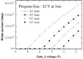
도 6은 본 발명의 바람직한 실시예에 따라 상기 도 2 및 도 3에 도시된 셀 트랜지스터의 읽기 동작을 설명하기 위한 그래프이다.FIG. 6 is a graph illustrating a read operation of the cell transistors illustrated in FIGS. 2 and 3 according to a preferred embodiment of the present invention.
상기 도 6에 도시된 특성 그래프는 상기 도 5에서 설명된 셀 트랜지스터의 조성 및 구조와 동일하다.The characteristic graph shown in FIG. 6 is identical to the composition and structure of the cell transistor described with reference to FIG. 5.
도 6을 참조하면, 프로그램 전압은 12V로 하여 하나의 제어 게이트에 대해 4개의 상태를 구현한다. 즉, 상태 ‘00’으로부터 상태 ‘11’까지의 상태를 구현할 수 있다.Referring to FIG. 6, four states are implemented for one control gate with a program voltage of 12V. That is, the state from the state '00' to the state '11' can be implemented.
읽기 동작의 경우, 상기 도 3에 도시된 드레인 선택 라인에 턴온 전압을 인가하고, 소스 선택 라인에도 턴온 전압을 인가한다. 따라서, 제1 최상위 워드 라인과 제1 최하위 워드 라인이 구비된 셀 트랜지스터에는 양의 전원 전압 VDD가 인가되고, 제32 최상위 워드라인 및 제32 최하위 워드 라인이 구비된 셀 트랜지스터에 는 접지 레벨이 인가된다.In the case of a read operation, a turn-on voltage is applied to the drain select line shown in FIG. 3 and a turn-on voltage is also applied to the source select line. Accordingly, a positive power supply voltage VDD is applied to the cell transistor including the first most significant word line and the first least significant word line, and a ground level is applied to the cell transistor including the thirty-second most significant word line and the thirty-second least significant word line. do.
특정의 트랜지스터에 프로그램된 데이터에 대해 읽기동작을 수행하고자 하는 경우, 선택된 트랜지스터 이외의 다른 트랜지스터들은 모두 턴온시킨다. 또한, 선택된 트랜지스터의 제어 게이트에는 소정의 읽기 전압을 인가한다. 선택된 트랜지스터에 프로그램된 상태에 따라 드레인 전류는 변경되므로 이를 통하여 프로그램된 데이터를 읽을 수 있다.When a read operation is performed on data programmed in a specific transistor, all transistors other than the selected transistor are turned on. In addition, a predetermined read voltage is applied to the control gate of the selected transistor. Since the drain current is changed according to the state programmed in the selected transistor, the programmed data can be read.
상기 도 6에서는 프로그램 전압을 12V로 한 경우, 세팅된 상태에 따라 제어 게이트의 전압 대비 드레인 전류를 측정한 것이다. 상기 도 6에서는 제어 게이트에 인가되는 읽기 전압이 약 2.8V 이상인 경우, 상태 ‘00’에서는 전류가 흐르지 않으며, 나머지 상태들에서는 서로 구별되는 양의 전류가 흐른다. 따라서, 도 6의 특성을 보이는 셀 트랜지스터에 대해서는 약 2.8V 이상의 읽기 전압의 인가가 바람직하다.In FIG. 6, when the program voltage is 12 V, the drain current is measured relative to the voltage of the control gate according to the set state. In FIG. 6, when the read voltage applied to the control gate is about 2.8 V or more, no current flows in the state '00', and a different amount of current flows in the remaining states. Therefore, application of a read voltage of about 2.8 V or more is desirable for the cell transistors exhibiting the characteristics of FIG. 6.
그러나, 본 실시예에 개시된 셀 트랜지스터에 대한 읽기 동작의 양상은 상술한 방법 이외에도 다양한 방법에 의해 구현될 수 있다.However, aspects of the read operation for the cell transistor disclosed in this embodiment can be implemented by various methods in addition to the above-described method.
또한, 읽기 동작의 순서는 선택된 셀 트랜지스터에 대해 2회의 읽기 동작이 수행된다. 예컨대, 상기 도 3에서 제2 최상위 워드라인과 제2 최하위 워드라인에 의해 제어되는 셀 트랜지스터에 프로그램된 데이터를 읽고자 하는 경우, 나머지 셀 트랜지스터들은 모두 턴온시킨다.In addition, in the order of the read operation, two read operations are performed on the selected cell transistor. For example, in FIG. 3, when the data programmed in the cell transistors controlled by the second highest word line and the second lowest word line is read, all remaining cell transistors are turned on.
먼저, 제2 최상위 워드라인에 읽기 전압을 인가하고, 제2 최하위 워드 라인은 플로팅 또는 0V 이하의 레벨을 유지하여 제2 최하위 워드 라인에 인가되는 전압 이 드레인 전류에 영향을 미치지 않도록 한다. 바람직하게는, 제2 최하위 워드 라인을 플로팅시켜서, 제2 최하위 워드 라인의 영향을 완전히 제거한다.First, a read voltage is applied to the second most significant word line, and the second least significant word line maintains a floating or level below 0V so that the voltage applied to the second least significant word line does not affect the drain current. Preferably, the second lowest word line is floated to completely eliminate the influence of the second lowest word line.
제2 최상위 워드라인에 인가된 읽기 전압에 따라 2비트로 프로그램된 데이터를 읽는다.Read data programmed in 2 bits according to the read voltage applied to the second most significant word line.
이어서, 동일한 원리로 제2 최하위 워드라인에 읽기 전압을 인가하고, 하위 비트에 해당하는 2비트에 대해 읽기 동작을 수행한다.Subsequently, a read voltage is applied to the second least significant word line, and a read operation is performed on two bits corresponding to the lower bits.
상술한 구성 및 동작에 따라, 하나의 셀 트랜지스터에는 4비트의 데이터가 프로그램될 수 있으며, 4비트의 데이터에 대해 읽기 동작은 2회에 걸쳐서 수행된다.According to the configuration and operation described above, four bits of data can be programmed in one cell transistor, and a read operation is performed twice for the four bits of data.
따라서, 적은 면적에 많은 데이터를 저장할 수 있으며, 저장된 데이터에 대해 빠른 속도의 읽기 동작을 수행할 수 있다.Therefore, a large amount of data can be stored in a small area, and a high speed read operation can be performed on the stored data.
또한, 본 발명에서는 부유 게이트가 실리콘 질화물로 구성되므로 실리콘 질화물의 계면에 트랩된 전자는 낮은 이동도를 가진다. 즉, 부유 게이트가 도전체인 다결정 실리콘이나 금속물인 경우보다 전자가 매우 낮은 이동도를 가지므로 제1 제어 게이트에 의해 트랩된 전자들은 제2 제어 게이트의 동작에 영향을 미치지 아니한다. 또한, 제1 제어 게이트 사이와 제2 제어 게이트 사이는 서로 이격되고, 이격 공간에는 부도체인 게이트간 유전막이 개재되므로 2개의 제어 게이트 사이의 영향력도 최소화된다. 따라서, 동일한 채널 영역 및 부유 게이트에 대해 서로 독립적인 프로그램 및 소거 동작이 가능해진다.In addition, in the present invention, since the floating gate is made of silicon nitride, electrons trapped at the interface of silicon nitride have low mobility. That is, the electrons trapped by the first control gate do not affect the operation of the second control gate because the electrons have a very low mobility than the case where the floating gate is a polycrystalline silicon or a metal material that is a conductor. In addition, the space between the first control gate and the second control gate is spaced apart from each other, and the inter-gate dielectric film, which is a non-conductor, is interposed in the space to minimize the influence between the two control gates. Thus, independent program and erase operations are possible for the same channel region and floating gate.
도 1은 종래 기술에 따른 플래시 메모리의 셀 트랜지스터를 도시한 단면도이다.1 is a cross-sectional view illustrating a cell transistor of a flash memory according to the prior art.
도 2는 본 발명의 실시예에 따른 플래시 메모리의 셀 트랜지스터를 도시한 단면도이다.2 is a cross-sectional view illustrating a cell transistor of a flash memory according to an embodiment of the present invention.
도 3a 내지 도 3d는 본 발명의 바람직한 실시예에 따라 상기 도 2에 도시된 플래시 메모리의 셀 트랜지스터를 형성하는 방법을 도시한 단면도들이다.3A to 3D are cross-sectional views illustrating a method of forming a cell transistor of the flash memory shown in FIG. 2 according to a preferred embodiment of the present invention.
도 4는 본 발명의 바람직한 실시예에 따라 상기 도 1에 도시된 셀 트랜지스터를 이용하여 구성한 낸드형 플래시 메모리의 평면도이다.4 is a plan view of a NAND flash memory constructed using the cell transistor shown in FIG. 1 according to a preferred embodiment of the present invention.
도 5는 본 발명의 바람직한 실시예에 따라 상기 도 2에 도시된 셀 트랜지스터에서 프로그램 시간에 따라 부유 게이트에 트랩되는 전하량을 도시한 그래프이다.5 is a graph showing the amount of charge trapped in the floating gate according to a program time in the cell transistor shown in FIG. 2 according to a preferred embodiment of the present invention.
도 6은 본 발명의 바람직한 실시예에 따라 상기 도 2 및 도 3에 도시된 셀 트랜지스터의 읽기 동작을 설명하기 위한 그래프이다.FIG. 6 is a graph illustrating a read operation of the cell transistors illustrated in FIGS. 2 and 3 according to a preferred embodiment of the present invention.
Claims (10)
Translated fromKoreanPriority Applications (2)
| Application Number | Priority Date | Filing Date | Title |
|---|---|---|---|
| KR1020070107807AKR100895854B1 (en) | 2007-10-25 | 2007-10-25 | Method of manufacturing flash memory having two control gates |
| US12/289,300US20090108327A1 (en) | 2007-10-25 | 2008-10-24 | Gate pattern having two control gates, flash memory including the gate pattern and methods of manufacturing and operating the same |
Applications Claiming Priority (1)
| Application Number | Priority Date | Filing Date | Title |
|---|---|---|---|
| KR1020070107807AKR100895854B1 (en) | 2007-10-25 | 2007-10-25 | Method of manufacturing flash memory having two control gates |
Publications (1)
| Publication Number | Publication Date |
|---|---|
| KR100895854B1true KR100895854B1 (en) | 2009-05-06 |
Family
ID=40581710
Family Applications (1)
| Application Number | Title | Priority Date | Filing Date |
|---|---|---|---|
| KR1020070107807AActiveKR100895854B1 (en) | 2007-10-25 | 2007-10-25 | Method of manufacturing flash memory having two control gates |
Country Status (2)
| Country | Link |
|---|---|
| US (1) | US20090108327A1 (en) |
| KR (1) | KR100895854B1 (en) |
Families Citing this family (1)
| Publication number | Priority date | Publication date | Assignee | Title |
|---|---|---|---|---|
| CN114497211B (en)* | 2020-10-23 | 2025-08-22 | 中芯北方集成电路制造(北京)有限公司 | Semiconductor structure and method for forming the same |
Citations (4)
| Publication number | Priority date | Publication date | Assignee | Title |
|---|---|---|---|---|
| KR20020082668A (en)* | 2001-04-25 | 2002-10-31 | 삼성전자 주식회사 | Non-Volatile Memory Device with 2 transistors for 2-bit operation |
| KR20060091120A (en)* | 2005-02-14 | 2006-08-18 | 삼성전자주식회사 | Nonvolatile Memory Device, Driving Method and Forming Method thereof |
| JP2006222367A (en) | 2005-02-14 | 2006-08-24 | Oki Electric Ind Co Ltd | Nonvolatile semiconductor memory device, driving method, and manufacturing method |
| KR20070006548A (en)* | 2005-07-07 | 2007-01-11 | 삼성전자주식회사 | Multi-bit storageable non-volatile memory device |
Family Cites Families (6)
| Publication number | Priority date | Publication date | Assignee | Title |
|---|---|---|---|---|
| KR100217901B1 (en)* | 1996-03-11 | 1999-09-01 | 김영환 | Flash Y pyrom cell and manufacturing method thereof |
| FR2871940B1 (en)* | 2004-06-18 | 2007-06-15 | St Microelectronics Rousset | TRANSISTOR MOS WITH FLOATING GRID, WITH DOUBLE CONTROL GRID |
| DE112004003019T5 (en)* | 2004-11-30 | 2008-01-03 | Spansion LLC, Santa Clara | Non-volatile memory device and method of making the same |
| JP4664771B2 (en)* | 2005-08-11 | 2011-04-06 | 株式会社東芝 | Semiconductor device and manufacturing method thereof |
| US7973366B2 (en)* | 2006-02-13 | 2011-07-05 | Macronix International Co., Ltd. | Dual-gate, sonos, non-volatile memory cells and arrays thereof |
| US7534732B1 (en)* | 2006-02-17 | 2009-05-19 | Spansion Llc | Semiconductor devices with copper interconnects and composite silicon nitride capping layers |
- 2007
- 2007-10-25KRKR1020070107807Apatent/KR100895854B1/enactiveActive
- 2008
- 2008-10-24USUS12/289,300patent/US20090108327A1/ennot_activeAbandoned
Patent Citations (4)
| Publication number | Priority date | Publication date | Assignee | Title |
|---|---|---|---|---|
| KR20020082668A (en)* | 2001-04-25 | 2002-10-31 | 삼성전자 주식회사 | Non-Volatile Memory Device with 2 transistors for 2-bit operation |
| KR20060091120A (en)* | 2005-02-14 | 2006-08-18 | 삼성전자주식회사 | Nonvolatile Memory Device, Driving Method and Forming Method thereof |
| JP2006222367A (en) | 2005-02-14 | 2006-08-24 | Oki Electric Ind Co Ltd | Nonvolatile semiconductor memory device, driving method, and manufacturing method |
| KR20070006548A (en)* | 2005-07-07 | 2007-01-11 | 삼성전자주식회사 | Multi-bit storageable non-volatile memory device |
Also Published As
| Publication number | Publication date |
|---|---|
| US20090108327A1 (en) | 2009-04-30 |
Similar Documents
| Publication | Publication Date | Title |
|---|---|---|
| CN100530600C (en) | Method of forming a non-volatile semiconductor memory device | |
| US8409951B2 (en) | Metal control gate formation in non-volatile storage | |
| CN100435296C (en) | Multi-bit non-volatile memory device and method thereof | |
| KR100847309B1 (en) | Manufacturing method of nonvolatile memory device | |
| US20080198669A1 (en) | Method of operating non-volatile memory | |
| KR20070100250A (en) | Ipyrom array with self-aligned shallow trench isolation | |
| JP7226987B2 (en) | Charge-trapping split-gate device and fabrication method thereof | |
| US10304680B1 (en) | Fabricating semiconductor devices having patterns with different feature sizes | |
| CN100481400C (en) | System and method for high density small memory array | |
| CN106024889B (en) | Semiconductor device and method for manufacturing the same | |
| US7164177B2 (en) | Multi-level memory cell | |
| JP2015537394A (en) | Charge trap split gate embedded flash memory and related methods | |
| JP2008227403A (en) | Semiconductor device and manufacturing method thereof | |
| US9252150B1 (en) | High endurance non-volatile memory cell | |
| JP6474349B2 (en) | High voltage gate formation | |
| US7485533B2 (en) | Fabrication method of an non-volatile memory | |
| US7602633B2 (en) | Non-volatile memory device, method of manufacturing the same, and method of operating the same | |
| US20160218227A1 (en) | Gate Formation Memory by Planarization | |
| KR100895854B1 (en) | Method of manufacturing flash memory having two control gates | |
| US7317222B2 (en) | Memory cell using a dielectric having non-uniform thickness | |
| US20140167136A1 (en) | Charge Trapping Device with Improved Select Gate to Memory Gate Isoloation | |
| US20070291551A1 (en) | Nonvolatitle memory array and method for operating thereof | |
| KR100540337B1 (en) | Gate Forming Method of Semiconductor Device | |
| KR20110065892A (en) | Flash memory device and manufacturing method thereof | |
| KR20060070049A (en) | Nonvolatile Memory Device and Manufacturing Method Thereof |
Legal Events
| Date | Code | Title | Description |
|---|---|---|---|
| A201 | Request for examination | ||
| PA0109 | Patent application | Patent event code:PA01091R01D Comment text:Patent Application Patent event date:20071025 | |
| PA0201 | Request for examination | ||
| E902 | Notification of reason for refusal | ||
| PE0902 | Notice of grounds for rejection | Comment text:Notification of reason for refusal Patent event date:20080827 Patent event code:PE09021S01D | |
| N231 | Notification of change of applicant | ||
| PN2301 | Change of applicant | Patent event date:20080925 Comment text:Notification of Change of Applicant Patent event code:PN23011R01D | |
| AMND | Amendment | ||
| E601 | Decision to refuse application | ||
| PE0601 | Decision on rejection of patent | Patent event date:20081114 Comment text:Decision to Refuse Application Patent event code:PE06012S01D Patent event date:20080827 Comment text:Notification of reason for refusal Patent event code:PE06011S01I | |
| AMND | Amendment | ||
| J201 | Request for trial against refusal decision | ||
| PJ0201 | Trial against decision of rejection | Patent event date:20081210 Comment text:Request for Trial against Decision on Refusal Patent event code:PJ02012R01D Patent event date:20081114 Comment text:Decision to Refuse Application Patent event code:PJ02011S01I Appeal kind category:Appeal against decision to decline refusal Decision date:20090204 Appeal identifier:2008101013159 Request date:20081210 | |
| PB0901 | Examination by re-examination before a trial | Comment text:Amendment to Specification, etc. Patent event date:20081210 Patent event code:PB09011R02I Comment text:Request for Trial against Decision on Refusal Patent event date:20081210 Patent event code:PB09011R01I Comment text:Amendment to Specification, etc. Patent event date:20081023 Patent event code:PB09011R02I | |
| B701 | Decision to grant | ||
| PB0701 | Decision of registration after re-examination before a trial | Patent event date:20090204 Comment text:Decision to Grant Registration Patent event code:PB07012S01D Patent event date:20090112 Comment text:Transfer of Trial File for Re-examination before a Trial Patent event code:PB07011S01I | |
| GRNT | Written decision to grant | ||
| PR0701 | Registration of establishment | Comment text:Registration of Establishment Patent event date:20090424 Patent event code:PR07011E01D | |
| PR1002 | Payment of registration fee | Payment date:20090427 End annual number:3 Start annual number:1 | |
| PG1601 | Publication of registration | ||
| FPAY | Annual fee payment | ||
| PR1001 | Payment of annual fee | Payment date:20120402 Start annual number:4 End annual number:4 | |
| FPAY | Annual fee payment | ||
| PR1001 | Payment of annual fee | Payment date:20130329 Start annual number:5 End annual number:5 | |
| PR1001 | Payment of annual fee | Payment date:20140331 Start annual number:6 End annual number:6 | |
| PR1001 | Payment of annual fee | Payment date:20150331 Start annual number:7 End annual number:7 | |
| FPAY | Annual fee payment | Payment date:20160630 Year of fee payment:8 | |
| PR1001 | Payment of annual fee | Payment date:20160630 Start annual number:8 End annual number:8 | |
| PR1001 | Payment of annual fee | Payment date:20170331 Start annual number:9 End annual number:9 | |
| PR1001 | Payment of annual fee | Payment date:20180330 Start annual number:10 End annual number:10 | |
| FPAY | Annual fee payment | Payment date:20190329 Year of fee payment:11 | |
| PR1001 | Payment of annual fee | Payment date:20190329 Start annual number:11 End annual number:11 | |
| PR1001 | Payment of annual fee | Payment date:20200330 Start annual number:12 End annual number:12 | |
| PR1001 | Payment of annual fee | Payment date:20210329 Start annual number:13 End annual number:13 | |
| PR1001 | Payment of annual fee | Payment date:20220323 Start annual number:14 End annual number:14 | |
| PR1001 | Payment of annual fee | Payment date:20230327 Start annual number:15 End annual number:15 | |
| PR1001 | Payment of annual fee | Payment date:20240325 Start annual number:16 End annual number:16 | |
| PR1001 | Payment of annual fee | Payment date:20250325 Start annual number:17 End annual number:17 |