KR100887072B1 - Semiconductor light emitting device, and semiconductor light emitting device package using same - Google Patents
Semiconductor light emitting device, and semiconductor light emitting device package using sameDownload PDFInfo
- Publication number
- KR100887072B1 KR100887072B1KR20070105327AKR20070105327AKR100887072B1KR 100887072 B1KR100887072 B1KR 100887072B1KR 20070105327 AKR20070105327 AKR 20070105327AKR 20070105327 AKR20070105327 AKR 20070105327AKR 100887072 B1KR100887072 B1KR 100887072B1
- Authority
- KR
- South Korea
- Prior art keywords
- conductive
- light emitting
- electrode layer
- layer
- emitting device
- Prior art date
- Legal status (The legal status is an assumption and is not a legal conclusion. Google has not performed a legal analysis and makes no representation as to the accuracy of the status listed.)
- Expired - Fee Related
Links
Images


Landscapes
- Led Device Packages (AREA)
- Led Devices (AREA)
Abstract
Translated fromKoreanDescription
Translated fromKorean본 발명은 반도체 발광소자 및 이를 이용한 반도체 발광소자 패키지에 관한 것으로서, 보다 상세하게는, 발광된 빛의 반사 또는 흡수를 최소화하고, 최대 발광면적을 확보하여 발광효율을 최대화하는 동시에 작은 면적의 전극으로 균일한 전류분산이 가능한, 신뢰성이 높고 저비용으로 양산성이 우수한 고품질의 반도체 발광소자 및 이를 이용한 반도체 발광소자 패키지에 관한 것이다.The present invention relates to a semiconductor light emitting device and a semiconductor light emitting device package using the same, and more particularly, to minimize the reflection or absorption of the emitted light, to secure the maximum light emitting area to maximize the luminous efficiency and at the same time small electrode The present invention relates to a high quality semiconductor light emitting device capable of uniform current distribution, high reliability and low mass production, and a semiconductor light emitting device package using the same.
발광소자는 소자 내에 포함되어 있는 물질이 빛을 발광하는 소자로서, 예를 들면, 발광다이오드(Light emitting diode, LED)와 같이 다이오드를 이용하여 반도체를 접합한 형태로 전자/정공 재결합에 따른 에너지를 광으로 변환하여 방출하는 소자가 있다. 이러한 발광소자는 현재 조명, 표시장치 및 광원으로서 널리 이용되며 그 개발이 가속화되고 있는 추세이다.A light emitting device is a device in which a material included in the device emits light. For example, a light emitting diode (LED) is used to bond energy of electron / hole recombination in the form of a semiconductor bonded using a diode. There is an element that converts and emits light. Such light emitting devices are widely used as lighting, display devices, and light sources, and their development is being accelerated.
특히, 최근 그 개발 및 사용이 활성화된 질화갈륨(GaN)계 발광다이오드를 이용한 휴대폰 키패드, 사이드 뷰어, 카메라 플래쉬 등의 상용화에 힘입어, 최근 발광다이오드를 이용한 일반 조명 개발이 활기를 띠고 있다. 대형 TV의 백라이트 유닛 및 자동차 전조등, 일반 조명 등 그의 응용제품이 소형 휴대제품에서 대형화, 고출력화, 고효율화, 신뢰성화된 제품으로 진행하여 해당 제품에 요구되는 특성을 나타내는 광원을 요구하게 되었다.In particular, the development of general lighting using light emitting diodes has recently been fueled by the commercialization of mobile phone keypads, side viewers, camera flashes, etc. using gallium nitride (GaN) based light emitting diodes, which have been actively developed and used. Its applications such as backlight units of large TVs, automotive headlamps, and general lighting have moved from small portable products to large size, high output, high efficiency, and reliable products, requiring light sources that exhibit the characteristics required for such products.
반도체 접합 발광소자 구조는 통상 p형 반도체 및 n형 반도체의 접합구조이다. 반도체 접합 구조에서는 양반도체의 접합영역에서 전자/정공 재결합에 따른 발광이 있을 수 있으나, 그 발광을 보다 활성화시키기 위한 활성층을 구비할 수도 있다. 이러한 반도체 접합 발광소자는 반도체층을 위한 전극의 위치에 따라 수평형 구조 및 수직형 구조가 있고, 수평형 구조에는 성장형(epi-up) 및 플립칩형(flip-chip)이 있다. 전술한 바와 같이 사용되는 제품의 특성상 각각 요구되는 발광소자의 구조적 특성이 중요하게 고려된다.The semiconductor junction light emitting device structure is usually a junction structure of a p-type semiconductor and an n-type semiconductor. In the semiconductor junction structure, there may be light emission due to electron / hole recombination in the junction region of both semiconductors, but an active layer for activating the light emission may be provided. The semiconductor junction light emitting device has a horizontal structure and a vertical structure according to the position of the electrode for the semiconductor layer, and there are growth-type (epi-up) and flip-chip (flip-chip) in the horizontal structure. In view of the characteristics of the product used as described above, the structural characteristics of each of the light emitting elements required are considered.
성장형 발광소자는 전극을 형성하기 위한 발광면적이 감소되는 문제가 있었고, 플립칩형 발광소자는 우수한 발광효율의 장점에도 불구하고, n형 전극 및 p형 전극을 동일평면상에 함께 배치하여 본딩하여야 하고, 본딩 후 전극접촉부와 전극과의 분리현상이 빈번하여 고가의 정밀한 공정장비가 요구되면서, 높은 제조비용, 낮은 생산성 및 낮은 수율과 제품신뢰성의 문제점이 있었다.The growth type light emitting device has a problem in that the light emitting area for forming the electrode is reduced, and the flip chip type light emitting device has to be bonded by bonding the n-type electrode and the p-type electrode together on the same plane in spite of the advantages of excellent light emission efficiency. As the separation between the electrode contact portion and the electrode after bonding is frequently required, expensive and precise process equipment is required, resulting in high manufacturing cost, low productivity, low yield, and product reliability.
또한, 수직형 반도체 발광소자는, 특히 고출력을 위한 대면적 발광소자를 제조하는 경우, 전류분산을 위하여 전극의 기판에 대한 면적비율이 높을 것이 요구된다. 그에 따라 광추출의 제한 및 광흡수로 인한 광손실 및 발광효율이 감소되고, 제품의 신뢰성이 저하되는 문제점이 있었다.In addition, in the case of manufacturing a large area light emitting device for high output, the vertical semiconductor light emitting device is required to have a high area ratio with respect to the substrate of the electrode for current dispersion. Accordingly, light loss and luminous efficiency due to the limitation of light extraction and light absorption are reduced, and there is a problem that the reliability of the product is lowered.
본 발명은 상술한 문제점을 해결하기 위한 것으로, 본 발명의 목적은 발광된 빛의 반사 또는 흡수를 최소화하고, 최대 발광면적을 확보하여 발광효율을 최대화하는 동시에 작은 면적의 전극으로 균일한 전류분산이 가능한, 신뢰성이 높고 저비용으로 양산성이 우수한 고품질의 반도체 발광소자 및 이를 이용한 반도체 발광소자 패키지를 제공함에 있다.The present invention is to solve the above problems, an object of the present invention is to minimize the reflection or absorption of the emitted light, to maximize the luminous efficiency by ensuring the maximum light emitting area and at the same time uniform current distribution to a small area of the electrode It is to provide a high quality semiconductor light emitting device and a semiconductor light emitting device package using the same which have high reliability and low cost.
이상과 같은 목적을 달성하기 위한 본 발명의 일 측면에 따른 반도체 발광소자는 제1도전형 반도체층, 활성층, 제2도전형 반도체층, 제2전극층, 전극절연부, 제1전극층 및 도전성 기판이 순차 적층된 반도체 발광소자로서, 도전성 기판은, 제1전극층과 접촉하는 제1도전성 기판, 제2도전성 기판 연결부를 통하여 제2전극층과 접촉하는 제2도전성 기판, 및 제1 및 제2도전성 기판을 전기적으로 분리하는 기판절연부를 포함하고, 제1전극층은, 제1도전형 반도체층에 전기적으로 접속되고 제2도전형 반도체층 및 활성층과는 전기적으로 절연되도록 제1전극층의 일면으로부터 제1도전형 반도체층의 적어도 일부 영역까지 연장된 하나 또는 그 이상의 콘택홀을 포함하고, 제2도전성 기판과는 전기적으로 절연되며, 제2전극층은 도전성 기판과 전기적으로 연결되고 제1 전극층과는 전기적으로 절연되도록 제1전극층을 관통하여 형성된 하나 또는 그 이상의 제2도전성 기판 연결부를 포함한다.In accordance with an aspect of the present invention, a semiconductor light emitting device includes a first conductive semiconductor layer, an active layer, a second conductive semiconductor layer, a second electrode layer, an electrode insulating portion, a first electrode layer, and a conductive substrate. A semiconductor light emitting device sequentially stacked includes a first conductive substrate in contact with a first electrode layer, a second conductive substrate in contact with a second electrode layer through a second conductive substrate connection portion, and first and second conductive substrates. A first insulating layer, wherein the first insulating layer is electrically connected to the first conductive semiconductor layer and electrically insulated from the second conductive semiconductor layer and the active layer. One or more contact holes extending to at least a portion of the semiconductor layer, the second electrode layer being electrically insulated from the second conductive substrate, the second electrode layer being electrically connected to the conductive substrate, One or more second conductive substrate connections formed through the first electrode layer to be electrically insulated from the first electrode layer.
제1 및 제2도전성 기판의 길이는 80 ㎛이고, 양 기판 사이의 기판절연부의 두께는 50 ㎛ 내지 100 ㎛일 수 있다.The length of the first and second conductive substrates is 80 μm, and the thickness of the substrate insulating portion between both substrates may be 50 μm to 100 μm.
제1 및 제2 도전성 기판은 Au, Ni, Cu, 및 W 중 어느 하나의 금속을 포함하는 금속성 기판일 수 있다.The first and second conductive substrates may be metallic substrates including any one of Au, Ni, Cu, and W metals.
제2전극층은 활성층으로부터 발생한 빛을 반사시키는 것이 바람직하며, 예를 들면, Ag, Al, 및 Pt 중 어느 하나의 금속을 포함할 수 있다.The second electrode layer preferably reflects light generated from the active layer, and may include, for example, a metal of any one of Ag, Al, and Pt.
본 발명의 다른 측면에 따르면, 상면에 홈부가 형성된 발광소자 패키지 본체; 패키지 본체에 장착되고, 홈부의 저면에 노출되고 서로 소정거리 이격되어 있는 제1리드프레임 및 제2리드프레임; 및 제1리드프레임 및 제2리드프레임 상에 실장되는 반도체 발광소자;를 포함하고, 반도체 발광소자는 제1도전형 반도체층, 활성층, 제2도전형 반도체층, 제2전극층, 전극절연부, 제1전극층 및 도전성 기판이 순차 적층되고, 도전성 기판은 제1전극층과 접촉하는 제1도전성 기판, 제2도전성 기판 연결부를 통하여 제2전극층과 접촉하는 제2도전성 기판, 및 제1 및 제2도전성 기판을 전기적으로 분리하는 기판절연부를 포함하고, 제1전극층은, 제1도전형 반도체층에 전기적으로 접속되고 제2도전형 반도체층 및 활성층과는 전기적으로 절연되도록 제1전극층의 일면으로부터 제1도전형 반도체층의 적어도 일부 영역까지 연장된 하나 또는 그 이상의 콘택홀을 포함하고, 제2전극층은 도전성 기판과 전기적으 로 연결되고 제1 전극층과는 전기적으로 절연되도록 제1전극층을 관통하여 형성된 하나 또는 그 이상의 제2도전성 기판 연결부를 포함하는 것을 특징으로 하는 반도체 발광소자 패키지가 제공된다.According to another aspect of the invention, the light emitting device package main body formed with a groove on the upper surface; A first lead frame and a second lead frame mounted on the package body and exposed to the bottom of the groove and spaced apart from each other by a predetermined distance; And a semiconductor light emitting device mounted on the first lead frame and the second lead frame, wherein the semiconductor light emitting device includes a first conductive semiconductor layer, an active layer, a second conductive semiconductor layer, a second electrode layer, an electrode insulating portion, The first electrode layer and the conductive substrate are sequentially stacked, and the conductive substrate is a first conductive substrate in contact with the first electrode layer, a second conductive substrate in contact with the second electrode layer through the second conductive substrate connection portion, and first and second conductive layers. And a substrate insulating portion for electrically separating the substrate, wherein the first electrode layer is electrically connected to the first conductive semiconductor layer and electrically insulated from the second conductive semiconductor layer and the active layer from one surface of the first electrode layer. One or more contact holes extending to at least a portion of the conductive semiconductor layer, wherein the second electrode layer is electrically connected to the conductive substrate and electrically insulated from the first electrode layer. The semiconductor light emitting device characterized in that a formed through the first electrode layer or the second conductive substrate comprises a further connection is provided.
기판절연부의 두께는 제1리드프레임 및 제2리드프레임의 사이의 간격과 동일하거나 큰 것이 바람직한데, 예를 들면, 기판절연부의 두께는 50 ㎛ 내지 100 ㎛일 수 있다.The thickness of the substrate insulator is preferably equal to or larger than the distance between the first lead frame and the second lead frame. For example, the thickness of the substrate insulator may be 50 μm to 100 μm.
이상 설명한 바와 같이 본 발명에 따른 반도체 발광소자는 발광방향에 위치하는 반도체층의 전극부를 발광면상에 모두 형성하지 않고, 그 일부를 제외하고는 활성층 아래에 형성하므로써, 발광된 빛이 전극부에 의하여 반사되거나 또는 흡수되는 현상을 방지할 수 있고, 발광면적 또한 최대로 확보할 수 있어 발광을 최대화할 수 있는 효과가 있다.As described above, the semiconductor light emitting device according to the present invention does not form all the electrode portions of the semiconductor layer located in the light emitting direction on the light emitting surface, except that a portion thereof is formed under the active layer, so that the emitted light is formed by the electrode portion. The phenomenon of being reflected or absorbed can be prevented, and the light emitting area can also be secured to the maximum, thereby maximizing light emission.
이외에도 전극부를 전류분산을 원활히 할 수 있도록 하나 또는 그 이상의 및 콘택홀을 구비하여 작은 면적의 전극으로 균일한 전류분산이 가능한 효과가 있다.In addition, the electrode unit is provided with one or more and contact holes so as to facilitate current distribution, and thus, it is possible to uniformly distribute current to electrodes having a small area.
또한, 도전성 기판이 각각의 전극과 접촉하고 있어서, 간단하게 다이본딩하여 패키지화 할 수 있으므로 저비용으로 우수한 양산성을 나타내는 효과가 있다.In addition, since the conductive substrate is in contact with each electrode and can be easily die-bonded and packaged, there is an effect of showing excellent mass productivity at low cost.
따라서, 본 발명에 따르면, 신뢰성이 높고 저비용으로 양산성이 우수한 고품질의 반도체 발광소자 및 반도체 발광소자 패키지를 구현할 수 있다.Therefore, according to the present invention, it is possible to implement a high quality semiconductor light emitting device and a semiconductor light emitting device package with high reliability and low cost.
이하, 첨부된 도면을 참조하여 본 발명의 실시형태를 설명한다. 그러나, 본 발명의 실시형태는 여러가지 다른 형태로 변형될 수 있으며, 본 발명의 범위가 이하 설명하는 실시형태로 한정되는 것은 아니다. 본 발명의 실시형태는 당업계에서 통상의 지식을 가진 자에게 본 발명을 보다 완전하게 설명하기 위해서 제공되는 것이다.Hereinafter, embodiments of the present invention will be described with reference to the accompanying drawings. However, embodiments of the present invention may be modified in various other forms, and the scope of the present invention is not limited to the embodiments described below. Embodiments of the present invention are provided to more fully describe the present invention to those skilled in the art.
도1은 본 발명의 일실시예에 따른 반도체 발광소자의 사시도이다.1 is a perspective view of a semiconductor light emitting device according to an embodiment of the present invention.
본 발명의 일실시예에 따른 반도체 발광소자(100)는 제1도전형 반도체층(110), 활성층(120), 제2도전형 반도체층(130), 제2전극층(140), 전극절연부(150), 제1전극층(160) 및 도전성 기판(171, 172, 180)이 순차 적층되어 있다. 도전성 기판(171, 172, 180)은, 제1전극층(160)과 접촉하는 제1도전성 기판(171), 제2도전성 기판 연결부(141)를 통하여 제2전극층(140)과 접촉하는 제2도전성 기판(172), 및 제1 및 제2도전성 기판(171, 172)을 전기적으로 분리하는 전극절연부(150)를 포함한다. 제1전극층(160)은, 제1도전형 반도체층(110)에 전기적으로 접속되고 제2도전형 반도체층(130) 및 활성층(120)는 전기적으로 절연되도록 제1전극 층(160)의 일면으로부터 제1도전형 반도체층(110)의 적어도 일부 영역까지 연장된 하나 또는 그 이상의 콘택홀(161)을 포함한다. 제2전극층(140)은 제2도전성 기판(172)과 전기적으로 연결되고 제1전극층(160)과는 전기적으로 절연되도록 제1전극층(160)을 관통하여 형성된 하나 또는 그 이상의 제2도전성 기판 연결부(141)를 포함한다.The semiconductor
반도체 발광소자(100)의 발광은 제1도전형 반도체층(110), 활성층(120), 및 제2도전형 반도체층(130)에서 수행된다. 즉, 반도체 발광소자(100)는 반도체층들(110, 130) 및 활성층과 함께, 제1도전형 반도체층(110)과 전기적으로 접속되는 제1전극층(160), 제2도전형 반도체층(130)과 전기적으로 접속되는 제2전극층(140), 및 전극층들(140, 160)을 전기적으로 절연시키기 위한 전극절연부(150)을 포함한다.Light emission of the semiconductor
각각의 반도체층(110, 130)은, 예를 들면, GaN계반도체, ZnO계반도체, GaAs계반도체, GaP계반도체, 및 GaAsP계반도체와 같은 무기반도체로 구성될 수 있다. 반도체층의 형성은 예를 들면, 분자선 에피택시(Molecular beam epitaxy, MBE)방법을 이용하여 수행될 수 있다. 이외에도, 반도체층들은 III-V 족 반도체, II-VI 족 반도체, 및 Si로 구성된 군으로부터 적절히 선택되어 구현될 수 있다. 반도체층들(110, 130)은 전술한 반도체에 각각의 도전형을 고려하여 적절한 불순물로 도핑된다.Each of the
활성층(120)은 발광을 활성화시키는 층으로서, 제1도전형 반도체층(110) 및 제2도전형 반도체층(130)의 에너지 밴드 갭보다 적은 에너지 밴드 갭을 갖는 물질을 이용하여 형성한다. 예를 들어 제1도전형 반도체층(110) 및 제2도전형 반도체층(130)이 GaN계 화합물 반도체인 경우, GaN의 에너지 밴드 갭보다 적은 에너지 밴드 갭을 갖는 InAlGaN계 화합물 반도체를 이용하여 활성층(120)을 형성할 수 있다. 즉, 활성층(120)은 InxAlyGa(1-x-y)N(0≤x≤1, 0≤y≤1, 0≤x+y≤1)일 수 있다.The
이때, 활성층(120)의 특성상, 불순물은 도핑되지 않는 것이 바람직하며, 구성물질의 몰비를 조절하여 발광하는 빛의 파장을 조절할 수도 있다. 따라서, 반도체 발광소자(100)는 활성층(120)의 특성에 따라 적외선, 가시광선, 및 자외선 중 어느 하나의 빛을 발광할 수 있다.At this time, it is preferable that the impurities are not doped due to the characteristics of the
전극층들(140, 160)은 각각 동일한 도전형의 반도체층에 전압을 인가하기 위한 층들이므로 전기전도성을 고려하여 금속을 포함할 수 있다. 즉, 전극층들(140, 160)은 반도체층들(110, 130)을 외부전원(미도시)과 전기적으로 연결하는 전극이다. 전극층들(140, 160)은 예를 들면, n형 전극으로는 Ti를, p형 전극으로는 Pd 또는 Au를 포함할 수 있다.Since the
제1전극층(160)은 제1도전형 반도체층(110)에, 제2전극층(140)은 제2도전형 반도체층(130)에 각각 접속되므로 서로 다른 도전형에 접속되는 특성상, 전극절연부(150)를 통하여 서로 전기적으로 분리된다. 전극절연부(150)은 전기전도성이 낮은 물질로 구성되는 것이 바람직하므로 예를 들어, SiO2와 같은 산화물을 포함할 수 있다.Since the
제1전극층(160)은, 제1도전형 반도체층(110)에 전기적으로 접속되고 제2도전형 반도체층(130) 및 활성층(120)는 전기적으로 절연되도록 제1전극층(160)의 일면으로부터 제1도전형 반도체층(110)의 적어도 일부 영역까지 연장된 하나 또는 그 이상의 콘택홀(161)을 포함한다.The
제2전극층(140)은 제2도전성 기판(172)과 전기적으로 연결되고 제1전극층(160)과는 전기적으로 절연되도록 제1전극층(160)을 관통하여 형성된 하나 또는 그 이상의 제2도전성 기판 연결부(141)를 포함한다. 콘택홀(161) 및 제2도전성 기판 연결부(141)에 대하여는 도3을 참조하여 이하 더 설명하기로 한다.One or more second conductive substrate connection portions formed through the
제2전극층(140)은 활성층(120)으로부터 발생한 빛을 반사시키는 것이 바람직하다. 제2전극층(140)은 활성층(120)의 하측에 위치하므로 활성층(120)을 기준으로 하여 반도체 발광소자(100)의 발광방향과 반대면에 위치한다. 활성층(120)으로부터 제2전극층(140)로 진행하는 반도체 발광소자(100)의 발광방향과 반대방향이고, 제2 전극층(140)을 향하여 진행하는 빛은 반사되어야 발광효율이 증가된다. 따라서, 제2전극층(140)이 광반사성을 나타낸다면 반사된 빛은 발광면으로 향하게 되고, 반도체 발광소자(100)의 발광효율이 증가된다.The
활성층(120)으로부터 발생한 빛을 반사시키기 위하여 제2전극층(140)은 가시광선영역에서 백색계열인 금속인 것이 바람직한데, 예를 들면, Ag, Al, 및 Pt 중 어느 하나일 수 있다.In order to reflect the light generated from the
도전성 기판(171, 172, 180)은, 제1전극층(160)과 접촉하는 제1도전성 기판(171), 제2도전성 기판 연결부(141)를 통하여 제2전극층(140)과 접촉하는 제2도전성 기판(172), 및 제1 및 제2도전성 기판(171, 172)을 전기적으로 분리하는 전극절연부(150)를 포함한다.The
제1도전성 기판(171) 및 제2도전성 기판(172)는 금속성 기판이거나 전도성 반도체 기판일 수 있다. 제1 및 제2도전성 기판(171, 172)이 금속인 경우, Au, Ni, Cu, 및 W 중 어느 하나의 금속으로 구성될 수 있다. 또한, 제1 및 제2도전성 기판(171, 172)이 반도체 기판인 경우, Si, Ge, 및 GaAs 중 어느 하나의 반도체 기판일 수 있다. 격자부정합이 비교적 낮은 사파이어 기판같은 부도전성 기판을 성장기판으로 사용한 후, 부도전성 기판을 제거하고 형성한다.The first
기판절연부(180)는 도전형이 서로 다른 제1 및 제2도전성 기판(171, 172)을 전기적으로 분리시킨다. 따라서, 전기전도성이 낮은 물질로 구성되는 것이 바람직하다. 예를 들어, 기판절연부(180)은 SiO2와 같은 산화물을 포함할 수 있다.The
도전성 기판(171, 172, 180)은 도금법 또는 기판접합법과 같은 공지의 방법을 이용하여 형성될 수 있다. 상술하면, 도금법은 씨드층을 형성하여 기판을 형성하거나, 도전성 기판(171, 172, 180)을 별도로 준비하여 Au, Au-Sn, 또는 Pb-Sr과 같은 도전성 접착제를 이용하여 제1전극층(160)에 접합시키는 기판접합법이 이용될 수 있다. 다만, 도전성 기판(171, 172, 180)이 전극층들(140, 160)을 외부전원(미도시)과 전기적으로 연결하기 위한 것이므로 소정길이로 형성되어야 하는 점을 고려하여 도금법을 이용하는 것이 바람직하다.The
도2a는 도1의 반도체 발광소자의 평면도이고, 도2b는 도1의 반도체 발광소자의 저면도이며, 도3은 도2a에 도시된 반도체 발광소자의 상면 중, A-A'선에서의 단면도이다.FIG. 2A is a plan view of the semiconductor light emitting device of FIG. 1, FIG. 2B is a bottom view of the semiconductor light emitting device of FIG. 1, and FIG. 3 is a cross-sectional view taken along the line A-A 'of the top surface of the semiconductor light emitting device shown in FIG. to be.
도2a를 참조하면, 반도체 발광소자(100)의 상면에는 실제 반도체 발광소자(100)의 상면에는 나타나지 않지만 콘택홀(161)의 위치를 표시하기 위하여 콘택홀(161)을 점선으로 도시하였다. 또한, 기판절연부(180)의 위치를 표시하기 위하여 B 및 B' 선을 이용하여 기판절연부(180)의 영역(130), 제1도전성 기판(171)의 영역(110) 및 제2도전성 기판(172)의 영역(130)을 표시하였다(도2b 참조).Referring to FIG. 2A, the
도2a에서 콘택홀(161)은 6개가 표시되어 있는데, 그 중, 3개는 제1도전성 기판 영역 상에, 나머지 3개는 제2도전성 기판 영역(120) 상에 위치하고 있다. 따라서, 제2도전성 기판 영역(120)상에 위치한 콘택홀(161)은 제1도전성 기판상의 콘택홀(161)과 소정의 배선부(162)를 이용하여 전기적으로 연결될 수 있다.In FIG. 2A, six
도3을 참조하면, 제1전극층(160)상에 형성된 콘택홀(161)이 도시되어 있다. 콘택홀(161)은 제1도전형 반도체층(110)에 전기적으로 접속되고 제2도전형 반도체층(130) 및 활성층(120)는 전기적으로 절연되도록 제1전극층(160)의 일면으로부터 제1도전형 반도체층(110)의 적어도 일부 영역까지 연장되어 있다.Referring to FIG. 3, a
콘택홀(161)은 제1전극층(160) 및 제2전극층(140)의 계면에서부터 제1도전형 반도체층(110) 내부까지 연장된다. 콘택홀(161)은 제2도전형 반도체층(130) 및 활성층(120)을 통과하여 제1도전형 반도체층(110)까지 연장되고, 적어도 활성층(120) 및 제1도전형 반도체층(110)의 계면까지는 연장된다. 바람직하게는 제1도전형 반도체층(110)의 일부까지 연장된다. 다만, 콘택홀(161)은 전기적 연결 및 전류분산을 위한 것이므로 제1도전형 반도체층(110)과 접촉하면 목적을 달성하므로 제1도전형 반도체층(110)의 외부표면까지 연장될 필요는 없다.The
콘택홀(161)은 제1도전형 반도체층(110)에 전류를 분산시키기 위한 것이므로 소정면적을 가져야 한다. 콘택홀(161)은 제1도전형 반도체층(110)상에 전류가 균일하게 분포될 수 있는 가능한 작은 면적으로 소정개수 형성되는 것이 바람직하다. 콘택홀(161)이 너무 적은 개수로 형성되면 전류분산이 어려워져 전기적 특성이 악화될 수 있고, 너무 많은 개수로 형성되면 형성을 위한 공정의 어려움 및 활성층의 감소로 인한 발광면적의 감소가 초래되므로 이러한 조건을 고려하여 그 개수는 적절히 선택될 수 있다. 따라서, 콘택홀(161)은 가능한 한 적은 면적을 차지하면서 전류분산이 효과적인 형상으로 구현된다.Since the
콘택홀(161)은 제2전극층(120)으로부터 제1도전형 반도체층(110) 내부까지 형성되는데, 제1도전형 반도체층의 전류분산을 위한 것이므로 제2도전형 반도체층(130) 및 활성층(120)과는 전기적으로 분리될 필요가 있다. 따라서, 제2전극층(120), 제2도전형 반도체층(130) 및 활성층(120)과 전기적으로 분리되는 것이 바람직하다. 따라서, 전극절연부(150)는 콘택홀(161)의 둘레를 감싸면서 연장될 수 있다. 이와 함께, 콘택홀(161)이 제2도전성 기판(172) 상측에 존재하는 경우, 제1전극층(160)은 제2도전성 기판(172)와 전기적으로 분리되는 것이 바람직하다.The
제2전극층(140)은 제2도전성 기판(172)과 전기적으로 연결되고 제1전극층(160)과는 전기적으로 절연되도록 제1전극층(160)을 관통하여 형성된 하나 또는 그 이상의 제2도전성 기판 연결부(141)를 포함한다. 도3에서, 제2도전성 기판 연결 부(141)는 제2전극층(140)과 점선으로 분리되도록 도시되어 있는데, 이는 제2도전성 기판 연결부(141)가 제2전극층(140)이 연장되어 형성될 수 있고, 또는 별도로 다른 전극물질을 사용하여 형성될 수 있음을 의미한다.One or more second conductive substrate connection portions formed through the
제2도전성 기판 연결부(141)를 통하여 제2전극층(140)은 제2도전성 기판(172)와 전기적으로 연결되고, 그에 따라 반도체 발광소자(100)는 활성층(120)으로부터 생성된 광의 발광방향에 별도의 본딩패드를 구비할 필요가 없어 보다 높은 광추출효율을 얻을 수 있다.The
제1 및 제2도전성 기판(171, 172)의 길이(l)는 80 ㎛ 이상인 것이 바람직한데, 제1 및 제2도전성 기판(171, 172)의 길이가 소정길이 이상인 경우 별도의 전극패드 없이 그대로 패키지에 장착할 수 있으므로 공정면에서 효율이 높다. 또한, 반도체 발광소자 패키지의 리드프레임 간 거리를 고려하여 양 기판(171, 172) 사이의 기판절연부(180)의 두께(d1)는 50 ㎛ 내지 100 ㎛일 수 있다. 다만, 기판절연부(180)의 두께는 적용할 패키지에 따라 조절될 수 있다.The length l of the first and second
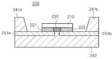
도4는 본 발명의 일실시예에 따른 반도체 발광소자 패키지의 단면도이다. 본 발명의 다른 측면에 따르면 반도체 발광소자 패키지(200)가 제공된다. 반도체 발광소자 패키지(200)는 상면에 홈부가 형성된 발광소자 패키지 본체(241a, 241b, 242); 패키지 본체(241a, 241b, 242)에 장착되고, 홈부의 저면에 노출되고 서로 소 정거리 이격되어 있는 제1리드프레임(251a) 및 제2리드프레임( 251b); 및 제1리드프레임(251a) 및 제2리드프레임(251b) 상에 실장되는 발광소자(210, 221, 222, 230);를 포함한다. 반도체 발광소자는 도1을 참조하여 설명한 본 발명의 일실시예에 따른 반도체 발광소자이다. 이하, 기설명한 동일 구성요소에 대하여는 설명을 생략하기로 한다.4 is a cross-sectional view of a semiconductor light emitting device package according to an embodiment of the present invention. According to another aspect of the present invention, a semiconductor light emitting
반도체 발광소자(210, 221, 222, 230)는 제1 및 제2반도체층, 활성층, 및 각각의 전극층을 포함하는 발광부(210) 및 도전성 기판(221, 222, 230)을 포함한다. 도전성 기판(221, 222, 230)에서 제1도전성 기판(211)은 제1리드프레임(251a)과 전기적으로 연결되고, 제2도전성 기판(172)은 제2리드프레임(252a)과 서로 접촉하도록 위치한다.The semiconductor
반도체 발광소자(210, 221, 222, 230)는 도전성 기판을 기판절연부(230)를 이용하여 전기적으로 분리하고 제1도전성 기판(221) 및 제2도전성 기판(222)을 각각의 도전성을 갖는 리드프레임에 연결함으로써 간단한 공정으로 실장할 수 있다. 본 발명에 따른 반도체 발광소자는 발광효율을 최대한 보장할 수 있으면서도 수직형 구조를 가지면서 비교적 간단한 다이본딩 형식으로 패키지상에 실장될 수 있다. 따라서, 비교적 저비용으로 공정수행이 가능하다.The semiconductor
이를 위하여, 기판절연부의 두께는 제1리드프레임 및 제2리드프레임의 사이 의 간격과 동일하거나 큰 것이 바람직하다. 예를 들면, 기판절연부의 두께는 50 ㎛ 내지 100 ㎛일 수 있다. 또한, 실장의 용이성을 고려하여, 도전성 기판(221, 222, 230)의 두께는 80 ㎛ 이상인 것이 바람직하다.For this purpose, the thickness of the substrate insulating portion is preferably equal to or greater than the distance between the first lead frame and the second lead frame. For example, the thickness of the substrate insulating portion may be 50 μm to 100 μm. In addition, in consideration of ease of mounting, the thickness of the
본 발명은 상술한 실시형태 및 첨부된 도면에 의해 한정되는 것이 아니라, 첨부된 청구범위에 의해 해석되어야 한다. 또한, 본 발명에 대하여 청구범위에 기재된 본 발명의 기술적 사상을 벗어나지 않는 범위 내에서 다양한 형태의 치환, 변형 및 변경이 가능하다는 것은 당해 기술분야의 통상의 지식을 가진 자에게 자명할 것이다.The invention is not to be limited by the foregoing embodiments and the accompanying drawings, but should be construed by the appended claims. In addition, it will be apparent to those skilled in the art that various forms of substitution, modification, and alteration are possible within the scope of the present invention without departing from the technical spirit of the present invention.
도1은 본 발명의 일실시예에 따른 반도체 발광소자의 사시도이다.1 is a perspective view of a semiconductor light emitting device according to an embodiment of the present invention.
도2a는 도1의 반도체 발광소자의 평면도이고, 도2b는 도1의 반도체 발광소자의 저면도이다.2A is a plan view of the semiconductor light emitting device of FIG. 1, and FIG. 2B is a bottom view of the semiconductor light emitting device of FIG.
도3은 도2a에 도시된 반도체 발광소자의 상면 중, A-A'선에서의 단면도이다.FIG. 3 is a cross-sectional view taken along line AA ′ of the top surface of the semiconductor light emitting device shown in FIG. 2A.
도4는 본 발명의 일실시예에 따른 반도체 발광소자 패키지의 단면도이다.4 is a cross-sectional view of a semiconductor light emitting device package according to an embodiment of the present invention.
<도면의 주요부분에 대한 부호의 설명><Description of the symbols for the main parts of the drawings>
100반도체 발광소자110제1도전형 반도체층100 Semiconductor
120활성층130제2도전형 반도체층120
140제2전극층150전극절연부140
160제1전극층171제1도전성 기판160
172제2도전성 기판173기판절연부172 Second conductive substrate 173 Substrate insulation
Claims (9)
Translated fromKoreanPriority Applications (1)
| Application Number | Priority Date | Filing Date | Title |
|---|---|---|---|
| KR20070105327AKR100887072B1 (en) | 2007-10-19 | 2007-10-19 | Semiconductor light emitting device, and semiconductor light emitting device package using same |
Applications Claiming Priority (1)
| Application Number | Priority Date | Filing Date | Title |
|---|---|---|---|
| KR20070105327AKR100887072B1 (en) | 2007-10-19 | 2007-10-19 | Semiconductor light emitting device, and semiconductor light emitting device package using same |
Publications (1)
| Publication Number | Publication Date |
|---|---|
| KR100887072B1true KR100887072B1 (en) | 2009-03-04 |
Family
ID=40697743
Family Applications (1)
| Application Number | Title | Priority Date | Filing Date |
|---|---|---|---|
| KR20070105327AExpired - Fee RelatedKR100887072B1 (en) | 2007-10-19 | 2007-10-19 | Semiconductor light emitting device, and semiconductor light emitting device package using same |
Country Status (1)
| Country | Link |
|---|---|
| KR (1) | KR100887072B1 (en) |
Cited By (4)
| Publication number | Priority date | Publication date | Assignee | Title |
|---|---|---|---|---|
| WO2010047553A3 (en)* | 2008-10-22 | 2010-07-29 | 삼성엘이디 주식회사 | Semiconductor light emitting device |
| KR20120002708A (en)* | 2010-07-01 | 2012-01-09 | 삼성엘이디 주식회사 | Semiconductor light emitting device |
| WO2014163369A1 (en)* | 2013-04-01 | 2014-10-09 | 주식회사 엘지화학 | Organic light emitting element and manufacturing method therefor |
| KR101798232B1 (en)* | 2010-07-07 | 2017-11-15 | 엘지이노텍 주식회사 | Light emitting device, method for fabricating the light emitting device, light emitting device package and lighting system |
Citations (1)
| Publication number | Priority date | Publication date | Assignee | Title |
|---|---|---|---|---|
| KR20060010527A (en)* | 2004-07-28 | 2006-02-02 | 삼성전기주식회사 | Nitride semiconductor light emitting device |
- 2007
- 2007-10-19KRKR20070105327Apatent/KR100887072B1/ennot_activeExpired - Fee Related
Patent Citations (1)
| Publication number | Priority date | Publication date | Assignee | Title |
|---|---|---|---|---|
| KR20060010527A (en)* | 2004-07-28 | 2006-02-02 | 삼성전기주식회사 | Nitride semiconductor light emitting device |
Cited By (13)
| Publication number | Priority date | Publication date | Assignee | Title |
|---|---|---|---|---|
| WO2010047553A3 (en)* | 2008-10-22 | 2010-07-29 | 삼성엘이디 주식회사 | Semiconductor light emitting device |
| US8008683B2 (en) | 2008-10-22 | 2011-08-30 | Samsung Led Co., Ltd. | Semiconductor light emitting device |
| US8686454B2 (en) | 2008-10-22 | 2014-04-01 | Samsung Electronics Co., Ltd. | Semiconductor light emitting device |
| US10333023B2 (en) | 2008-10-22 | 2019-06-25 | Samsung Electronics Co., Ltd. | Method of manufacturing semiconductor light emitting device |
| US8975653B2 (en) | 2008-10-22 | 2015-03-10 | Samsung Electronics Co., Ltd. | Semiconductor light emitting device |
| US9997663B2 (en) | 2008-10-22 | 2018-06-12 | Samsung Electronics Co., Ltd. | Semiconductor light emitting device |
| US9680050B2 (en) | 2008-10-22 | 2017-06-13 | Samsung Electronics Co., Ltd. | Semiconductor light emitting device |
| KR20120002708A (en)* | 2010-07-01 | 2012-01-09 | 삼성엘이디 주식회사 | Semiconductor light emitting device |
| KR101711960B1 (en)* | 2010-07-01 | 2017-03-06 | 삼성전자주식회사 | Semiconductor light emitting device |
| KR101798232B1 (en)* | 2010-07-07 | 2017-11-15 | 엘지이노텍 주식회사 | Light emitting device, method for fabricating the light emitting device, light emitting device package and lighting system |
| US9825249B2 (en) | 2013-04-01 | 2017-11-21 | Lg Display Co., Ltd. | Organic light emitting device and method for manufacturing the same |
| CN105103330A (en)* | 2013-04-01 | 2015-11-25 | 株式会社Lg化学 | Organic light emitting device and manufacturing method thereof |
| WO2014163369A1 (en)* | 2013-04-01 | 2014-10-09 | 주식회사 엘지화학 | Organic light emitting element and manufacturing method therefor |
Similar Documents
| Publication | Publication Date | Title |
|---|---|---|
| KR100891761B1 (en) | Semiconductor light emitting device, manufacturing method thereof and semiconductor light emitting device package using same | |
| KR100849826B1 (en) | Light emitting device and package containing same | |
| KR101891257B1 (en) | Light Emitting Device and Manufacturing Method thereof | |
| KR101144351B1 (en) | wafer level LED package and fabrication method thereof | |
| EP2355177B1 (en) | Light emitting device, method of manufacturing the same | |
| KR100818466B1 (en) | Semiconductor light emitting device | |
| JP6199948B2 (en) | Light emitting device, light emitting device package | |
| KR101276053B1 (en) | Semiconductor light emitting device and light emitting apparatus | |
| KR101047720B1 (en) | Light emitting device, method of manufacturing light emitting device, | |
| KR20120039587A (en) | Wafer level led package | |
| KR100887072B1 (en) | Semiconductor light emitting device, and semiconductor light emitting device package using same | |
| KR101064064B1 (en) | Light emitting element | |
| CN107949920A (en) | Luminescent device and the light emitting device package comprising the luminescent device | |
| TWI453952B (en) | Light emitting element and manufacturing method thereof | |
| KR101411256B1 (en) | Semiconductor light emitting device and manufacturing method thereof | |
| US9362718B2 (en) | Semiconductor light emitting device | |
| US9236304B2 (en) | Semiconductor light emitting device and method of manufacturing the same | |
| KR20120014972A (en) | Light emitting device, light emitting device manufacturing method, light emitting device package, and lighting system | |
| KR102261951B1 (en) | Semiconductor device and semiconductor device manufacturing method | |
| CN101820038B (en) | Semiconductor light emitting device, manufacturing method, and semiconductor light emitting device package | |
| KR20120022091A (en) | Light emitting device, method for fabricating the light emitting device, light emitting device package and lighting system | |
| KR20120045635A (en) | Light emitting device, method for fabricating the light emitting device, light emitting device package and lighting system | |
| KR20180090529A (en) | Semiconductor device package | |
| KR102162438B1 (en) | Light emitting device | |
| KR102320865B1 (en) | Light emitting device |
Legal Events
| Date | Code | Title | Description |
|---|---|---|---|
| A201 | Request for examination | ||
| PA0109 | Patent application | St.27 status event code:A-0-1-A10-A12-nap-PA0109 | |
| PA0201 | Request for examination | St.27 status event code:A-1-2-D10-D11-exm-PA0201 | |
| E902 | Notification of reason for refusal | ||
| PE0902 | Notice of grounds for rejection | St.27 status event code:A-1-2-D10-D21-exm-PE0902 | |
| P11-X000 | Amendment of application requested | St.27 status event code:A-2-2-P10-P11-nap-X000 | |
| P13-X000 | Application amended | St.27 status event code:A-2-2-P10-P13-nap-X000 | |
| P22-X000 | Classification modified | St.27 status event code:A-2-2-P10-P22-nap-X000 | |
| E701 | Decision to grant or registration of patent right | ||
| PE0701 | Decision of registration | St.27 status event code:A-1-2-D10-D22-exm-PE0701 | |
| GRNT | Written decision to grant | ||
| PR0701 | Registration of establishment | St.27 status event code:A-2-4-F10-F11-exm-PR0701 | |
| PR1002 | Payment of registration fee | St.27 status event code:A-2-2-U10-U11-oth-PR1002 Fee payment year number:1 | |
| PG1601 | Publication of registration | St.27 status event code:A-4-4-Q10-Q13-nap-PG1601 | |
| PN2301 | Change of applicant | St.27 status event code:A-5-5-R10-R11-asn-PN2301 | |
| PN2301 | Change of applicant | St.27 status event code:A-5-5-R10-R14-asn-PN2301 | |
| R18-X000 | Changes to party contact information recorded | St.27 status event code:A-5-5-R10-R18-oth-X000 | |
| PR1001 | Payment of annual fee | St.27 status event code:A-4-4-U10-U11-oth-PR1001 Fee payment year number:4 | |
| PN2301 | Change of applicant | St.27 status event code:A-5-5-R10-R11-asn-PN2301 | |
| PN2301 | Change of applicant | St.27 status event code:A-5-5-R10-R14-asn-PN2301 | |
| FPAY | Annual fee payment | Payment date:20130131 Year of fee payment:5 | |
| PR1001 | Payment of annual fee | St.27 status event code:A-4-4-U10-U11-oth-PR1001 Fee payment year number:5 | |
| FPAY | Annual fee payment | Payment date:20140129 Year of fee payment:6 | |
| PR1001 | Payment of annual fee | St.27 status event code:A-4-4-U10-U11-oth-PR1001 Fee payment year number:6 | |
| R18-X000 | Changes to party contact information recorded | St.27 status event code:A-5-5-R10-R18-oth-X000 | |
| FPAY | Annual fee payment | Payment date:20150202 Year of fee payment:7 | |
| PR1001 | Payment of annual fee | St.27 status event code:A-4-4-U10-U11-oth-PR1001 Fee payment year number:7 | |
| PR1001 | Payment of annual fee | St.27 status event code:A-4-4-U10-U11-oth-PR1001 Fee payment year number:8 | |
| PR1001 | Payment of annual fee | St.27 status event code:A-4-4-U10-U11-oth-PR1001 Fee payment year number:9 | |
| P22-X000 | Classification modified | St.27 status event code:A-4-4-P10-P22-nap-X000 | |
| LAPS | Lapse due to unpaid annual fee | ||
| PC1903 | Unpaid annual fee | St.27 status event code:A-4-4-U10-U13-oth-PC1903 Not in force date:20180227 Payment event data comment text:Termination Category : DEFAULT_OF_REGISTRATION_FEE | |
| PC1903 | Unpaid annual fee | St.27 status event code:N-4-6-H10-H13-oth-PC1903 Ip right cessation event data comment text:Termination Category : DEFAULT_OF_REGISTRATION_FEE Not in force date:20180227 | |
| R18-X000 | Changes to party contact information recorded | St.27 status event code:A-5-5-R10-R18-oth-X000 | |
| P22-X000 | Classification modified | St.27 status event code:A-4-4-P10-P22-nap-X000 |