KR100886644B1 - Calibration Circuit with On Die Termination Device - Google Patents
Calibration Circuit with On Die Termination DeviceDownload PDFInfo
- Publication number
- KR100886644B1 KR100886644B1KR1020070087070AKR20070087070AKR100886644B1KR 100886644 B1KR100886644 B1KR 100886644B1KR 1020070087070 AKR1020070087070 AKR 1020070087070AKR 20070087070 AKR20070087070 AKR 20070087070AKR 100886644 B1KR100886644 B1KR 100886644B1
- Authority
- KR
- South Korea
- Prior art keywords
- calibration
- fuse
- code
- node
- circuit
- Prior art date
- Legal status (The legal status is an assumption and is not a legal conclusion. Google has not performed a legal analysis and makes no representation as to the accuracy of the status listed.)
- Expired - Fee Related
Links
Images


Classifications
- G—PHYSICS
- G11—INFORMATION STORAGE
- G11C—STATIC STORES
- G11C7/00—Arrangements for writing information into, or reading information out from, a digital store
- G11C7/10—Input/output [I/O] data interface arrangements, e.g. I/O data control circuits, I/O data buffers
- G11C7/1051—Data output circuits, e.g. read-out amplifiers, data output buffers, data output registers, data output level conversion circuits
- G—PHYSICS
- G11—INFORMATION STORAGE
- G11C—STATIC STORES
- G11C7/00—Arrangements for writing information into, or reading information out from, a digital store
- G11C7/10—Input/output [I/O] data interface arrangements, e.g. I/O data control circuits, I/O data buffers
- G—PHYSICS
- G11—INFORMATION STORAGE
- G11C—STATIC STORES
- G11C17/00—Read-only memories programmable only once; Semi-permanent stores, e.g. manually-replaceable information cards
- G11C17/14—Read-only memories programmable only once; Semi-permanent stores, e.g. manually-replaceable information cards in which contents are determined by selectively establishing, breaking or modifying connecting links by permanently altering the state of coupling elements, e.g. PROM
- G11C17/18—Auxiliary circuits, e.g. for writing into memory
- G—PHYSICS
- G11—INFORMATION STORAGE
- G11C—STATIC STORES
- G11C29/00—Checking stores for correct operation ; Subsequent repair; Testing stores during standby or offline operation
- G11C29/02—Detection or location of defective auxiliary circuits, e.g. defective refresh counters
- G11C29/022—Detection or location of defective auxiliary circuits, e.g. defective refresh counters in I/O circuitry
- G—PHYSICS
- G11—INFORMATION STORAGE
- G11C—STATIC STORES
- G11C29/00—Checking stores for correct operation ; Subsequent repair; Testing stores during standby or offline operation
- G11C29/02—Detection or location of defective auxiliary circuits, e.g. defective refresh counters
- G11C29/025—Detection or location of defective auxiliary circuits, e.g. defective refresh counters in signal lines
- G—PHYSICS
- G11—INFORMATION STORAGE
- G11C—STATIC STORES
- G11C29/00—Checking stores for correct operation ; Subsequent repair; Testing stores during standby or offline operation
- G11C29/02—Detection or location of defective auxiliary circuits, e.g. defective refresh counters
- G11C29/028—Detection or location of defective auxiliary circuits, e.g. defective refresh counters with adaption or trimming of parameters
- G—PHYSICS
- G11—INFORMATION STORAGE
- G11C—STATIC STORES
- G11C7/00—Arrangements for writing information into, or reading information out from, a digital store
- G11C7/10—Input/output [I/O] data interface arrangements, e.g. I/O data control circuits, I/O data buffers
- G11C7/1051—Data output circuits, e.g. read-out amplifiers, data output buffers, data output registers, data output level conversion circuits
- G11C7/1057—Data output buffers, e.g. comprising level conversion circuits, circuits for adapting load
- G—PHYSICS
- G11—INFORMATION STORAGE
- G11C—STATIC STORES
- G11C2207/00—Indexing scheme relating to arrangements for writing information into, or reading information out from, a digital store
- G11C2207/22—Control and timing of internal memory operations
- G11C2207/2254—Calibration
Landscapes
- Semiconductor Integrated Circuits (AREA)
- Logic Circuits (AREA)
Abstract
Translated fromKoreanDescription
Translated fromKorean본 발명은 반도체 메모리장치와 같은 각종 반도체 집적회로에 사용되는 온 다이 터미네이션(On Die Termination) 장치에 관한 것으로, 상세하게는 온 다이 터미네이션 장치에서 발생하는 오차를 더욱 용이하게 보정하기 위한 것이다.BACKGROUND OF THE INVENTION 1. Field of the Invention The present invention relates to an on die termination device used in various semiconductor integrated circuits such as a semiconductor memory device, and more particularly, to more easily correct an error occurring in the on die termination device.
CPU, 메모리 및 게이트 어레이 등과 같이 집적회로 칩으로 구현되는 다양한 반도체장치들(Semiconductor Devices)은 퍼스널 컴퓨터, 서버 또는 워크스테이션과 같은 다양한 전기적 제품(electrical products) 내로 합체되어 진다. 대부분의 경우에, 상기 반도체장치는 외부(outside world)에서 전송되는 각종 신호들을 입력 패드를 통해 수신하기 위한 수신회로와 내부의 신호를 출력 패드를 통해 외부로 제공하기 위한 출력회로를 가지고 있다.Various semiconductor devices implemented as integrated circuit chips, such as CPUs, memories and gate arrays, are incorporated into various electrical products such as personal computers, servers or workstations. In most cases, the semiconductor device has a receiving circuit for receiving various signals transmitted from the outside world through an input pad and an output circuit for providing an internal signal to the outside through an output pad.
한편, 전기적 제품의 동작 스피드가 고속화 됨에 따라 상기 반도체 장치들간에 인터페이스되는 신호의 스윙폭은 점차로 줄어들고 있다. 그 이유는 신호전달에 걸리는 지연시간을 최소화하기 위해서이다. 그러나 신호의 스윙 폭이 줄어들수록 외부 노이즈에 대한 영향은 증가되고, 인터페이스단에서 임피던스 미스매칭(impedance mismatching, '부정합' 이라고도 함)에 따른 신호의 반사도 심각해 진다. 상기 임피던스 미스매칭은 외부 노이즈나 전원전압의 변동, 동작온도의 변화, 제조공정의 변화등에 기인하여 발생된다. 임피던스 미스매칭이 발생되면 데이터의 고속전송이 어렵게 되고 반도체장치의 데이터 출력단으로부터 출력되는 출력 데이터가 왜곡될 수 있다. 따라서, 수신 측의 반도체장치가 상기 왜곡된 출력신호를 입력단으로 수신할 경우 셋업/홀드 페일(setup/hold fail) 또는 입력레벨의 판단미스 등의 문제들이 빈번히 야기될 수 있다.Meanwhile, as the operating speed of an electrical product is increased, the swing width of a signal interfaced between the semiconductor devices is gradually reduced. The reason is to minimize the delay time for signal transmission. However, as the swing width of the signal decreases, the influence on external noise increases, and the reflection of the signal due to impedance mismatching (also referred to as mismatch) at the interface stage becomes more severe. The impedance mismatch occurs due to external noise, fluctuations in power supply voltage, change in operating temperature, change in manufacturing process, or the like. When impedance mismatching occurs, high-speed data transfer is difficult and output data output from the data output terminal of the semiconductor device may be distorted. Therefore, when the semiconductor device on the receiving side receives the distorted output signal to the input terminal, problems such as setup / hold fail or input level determination error may occur frequently.
특히, 동작스피드의 고속화가 요구되는 메모리장치는 상술한 문제들의 해결을 위해 온 다이 터미네이션이라 불리우는 임피던스 매칭회로를 집적회로 칩내의 패드 근방에 채용하고 있다. 통상적으로 온 다이 터미네이션 스킴에 있어서, 전송측에서는 출력회로에 의한 소오스 터미네이션(Source Termination)이 행해지고, 수신측에서는 상기 입력 패드에 연결된 수신회로에 대하여 병렬로 연결되어진 터미네이션 회로에 의해 병렬 터미네이션이 행해진다.In particular, a memory device requiring high speed of operation employs an impedance matching circuit called on die termination in the vicinity of a pad in an integrated circuit chip to solve the above problems. In general, in an on die termination scheme, source termination is performed by an output circuit on the transmission side, and parallel termination is performed by a termination circuit connected in parallel to a receiving circuit connected to the input pad on the receiving side.
ZQ캘리브래이션(ZQ calibration)이란 PVT(Process, Voltage, Temperature: 프로세스, 전압 , 온도)조건이 변함에 따라 변화하는 풀업 및 풀다운 코드를 생성하는 과정을 말하는데, ZQ캘리브래이션 결과로 생성된 상기 코드들을 이용하여 온 다이 터미네이션 장치의 저항값(메모리장치의 경우에는 DQ패드 쪽의 터미네이션 저항값)을 조정하게 된다.(캘리브래이션을 위한 노드인 ZQ노드를 이용해서 캘리브래 이션이 이루어지기 때문에 ZQ캘리브래이션이라 한다.)ZQ calibration refers to a process of generating pull-up and pull-down codes that change as the PVT (Process, Voltage, Temperature) process changes. The ZQ calibration results from the ZQ calibration. The codes are used to adjust the resistance value of the on-die termination device (the termination resistance value on the DQ pad side in the case of a memory device) (since calibration is performed using the ZQ node, which is a node for calibration). It is called ZQ calibration.)
이하, 온 다이 터미네이션 장치에서 행해지는 ZQ캘리브래이션에 대해 알아본다.Hereinafter, the ZQ calibration performed in the on die termination device will be described.
도 1은 종래의 온 다이 터미네이션 장치에서 ZQ캘리브래이션 동작을 수행하는 캘리브래이션 회로의 구성도이다.1 is a configuration diagram of a calibration circuit for performing a ZQ calibration operation in a conventional on-die termination device.
도면에 도시된 바와 같이, 종래의 온 다이 터미네이션 장치는 제1캘리브래이션 저항부(110), 더미 캘리브래이션 저항부(120), 제2캘리브래이션 저항부(130), 기준전압 발생기(102), 비교기(103, 104), 카운터(105, 106)를 포함하여 ZQ 캘리브래이션 동작을 수행한다. 제1캘리브래이션 저항부(110)는 풀업 캘리브래이션 코드(PCODE<0:N>)를 입력받아 온/오프되는 다수의 풀업저항을 포함해 구성된다. 그리고 더미 캘리브래이션 저항부(120)는 제1캘리브래이션 저항부(110)와 동일하게 구성되며, 풀다운 캘리브래이션 저항부(130)는 풀다운 캘리브래이션 코드(NCODE<0:N>)를 입력받아 온/오프되는 다수의 풀다운저항을 포함해 구성된다.As shown in the drawing, the conventional on-die termination device includes a
제1캘리브래이션 저항부(110)는 ZQ노드에 연결된 외부저항(101)과 캘리브래이션 되면서 1차적인 캘리브래이션 코드(PCODE<0:N>)를 생성하기 위한 것이며, 제2캘리브래이션 저항부(130)는 제1캘리브래이션 저항부(110)를 통해 생성된 캘리브래이션 코드(PCODE<0:N>)를 이용하여 두번째의 캘리브래이션 코드(NCODE<0:N>)를 생성하기 위한 것이다. 그리고 그 과정에서 제1캘리브래이션 저항부(110)와 동일한 저항값을 갖게 되는 더미 캘리브래이션 저항부(120)가 사용된다.The first
그 동작을 보면, 비교기(comparator)(103)는 ZQ핀(ZQ노드의 칩 외부)에 연결 된 외부저항(101)(일반적으로 240Ω)과 제1캘리브래이션 저항부(110)를 연결하여 생성되는 ZQ노드의 전압과 내부의 기준전압 발생기(102)에서 생성되는 기준전압(VREF, 일반적으로 VDDQ/2로 설정됨)을 비교하여 업/다운(UP/DOWN) 신호를 생성한다.In operation, a
풀업카운터(105)는 상기 업/다운 신호를 받아서 이진코드(PCODE<0:N>)를 생성하는데, 생성된 이진코드(PCODE<0:N>)로 제1캘리브래이션 저항부(110)의 병렬로 연결된 저항들을 온/오프하여 저항값을 조정한다. 조정된 제1캘리브래이션 저항부(110)의 저항값은 다시 ZQ노드의 전압에 영향을 주고 상기한 바와 같은 동작이 반복된다. 즉, 제1캘리브래이션 저항부(110)의 전체 저항값이 외부저항(101)(일반적으로 240Ω)의 저항값과 같아지도록 제1캘리브래이션 저항부(110)가 캘리브래이션(calibration) 된다.(풀업 캘리브래이션)The pull-
상술한 풀업 캘리브래이션 과정 중에 생성되는 이진코드(PCODE<0:N>, 풀업 캘리브래이션 코드)는 더미 캘리브래이션 저항부(120)에 입력되어 풀업 캘리브래이션 저항부(120)의 전체 저항값을 결정하게 된다(제1캘리브래이션 저항부, 외부저항과 동일한 저항값을 갖는다). 이제 풀다운 캘리브래이션 동작이 시작되는데 풀업 캘리브래이션의 경우와 비슷하게, 비교기(104)와 풀다운카운터(106)를 사용하여 a노드의 전압이 기준전압(VREF)과 같아지도록, 즉 제2캘리브래이션 저항부(130)의 전체 저항값이 더미 캘리브래이션 저항부(120)의 전체 저항값과 같아지도록 캘리브래이션 된다.(풀다운 캘리브래이션)The binary code (PCODE <0: N>, pull-up calibration code) generated during the above-described pull-up calibration process is input to the
상술한 ZQ캘리브래이션(풀업 및 풀다운 캘리브래이션)의 결과로 생성된 이진 코드들(PCODE<0:N>, NCODE<0:N>)은, 도 1의 캘리브래이션 회로의 풀업 및 풀다운 캘리브래이션 저항부와 동일하게 레이아웃 되어있는 입/출력 패드 측의 풀업 및 풀다운저항(터미네이션 저항)에 입력되어 온 다이 터미네이션 장치의 저항값을 결정하게 된다.(메모리장치의 경우에는 DQ패드 측에 있는 풀업 및 풀다운 터미네이션 저항값을 결정)The binary codes PCODE <0: N> and NCODE <0: N> generated as a result of the above-described ZQ calibration (pull-up and pull-down calibration) are the pull-up and pull-down of the calibration circuit of FIG. The resistance value of the die termination device input to the pull-up and pull-down resistors (termination resistors) on the input / output pad side laid out in the same way as the calibration resistor unit is determined. Determine pull-up and pull-down termination resistors)
참고로, 상술한 종래기술에는 풀업 및 풀다운 캘리브래이션을 모두 실시해 풀업 캘리브래이션 코드(PCODE<0:N>)와 풀다운 캘리브래이션 코드(NCODE<0:N>)를 생성해 온 다이 터미네이션 장치의 풀업 터미네이션 저항부와 풀다운 터미내이션 저항부의 저항값을 결정하는 경우에 대해 설명했지만, 온 다이 터미네이션 장치에서 항상 풀업 터미네이션 저항부와 풀다운 터미네이션 저항부 모두를 구비하고 있는 것은 아니다. 예를 들어, 반도체 메모리장치의 경우에는 출력드라이버 측에는 풀업 터미네이션 저항부와 풀다운 터미네이션 저항부를 모두 사용하고 있지만, 입력버퍼 측에는 풀업 터미네이션 저항부만을 사용하고 있다.For reference, in the above-described conventional technique, both the pull-up and pull-down calibration are performed to generate a die termination for generating a pull-up calibration code (PCODE <0: N>) and a pull-down calibration code (NCODE <0: N>). Although the case of determining the resistance values of the pull-up termination resistors and pull-down termination resistors of the device has been described, the on-die termination device does not always include both the pull-up termination resistors and the pull-down termination resistors. For example, in the case of a semiconductor memory device, both a pull-up termination resistor and a pull-down termination resistor are used on the output driver side, but only a pull-up termination resistor is used on the input buffer side.
따라서 온 다이 터미네이션 장치가 입/출력패드 측에 풀업 터미네이션 저항부만으로 구성된 경우에는, 도 1의 캘리브래이션 회로에서도, 풀업 캘리브래이션 코드(PCODE<0:N>)를 생성하기 위한 부분인 풀업 캘리브래이션 저항부(110), 카운터(105), 비교기(103)만으로 구성되면 된다. 그리고 그때의 동작은 상술한 풀업 캘리브래이션 과정과 동일하다.Therefore, when the on-die termination device is composed of only a pull-up termination resistor on the input / output pad side, the pull-up which is a part for generating the pull-up calibration code (PCODE <0: N>) also in the calibration circuit of FIG. It is sufficient to consist only of the
도 2는 온 다이 터미네이션 장치가 반도체 메모리장치에 적용된 예를 도시한 것으로, 도 1의 캘리브래이션 회로에서 생성한 캘리브래이션 코드(PCODE<0:N>, NCODE<0:N>)를 이용해 출력드라이버의 터미네이션 저항값을 결정하는 것을 나타내는 도면이다. 즉, 온 다이 터미네이션 장치의 캘리브래이션 회로가 도 1이 되고, 온 다이 터미네이션 장치의 터미네이션 회로가 출력드라이버(도 2)가 되는 예를 도시하였다.FIG. 2 illustrates an example in which an on die termination device is applied to a semiconductor memory device, using calibration codes PCODE <0: N> and NCODE <0: N> generated by the calibration circuit of FIG. 1. The figure which shows the determination of the termination resistance value of an output driver. That is, an example is shown in which the calibration circuit of the on die termination device is shown in FIG. 1 and the termination circuit of the on die termination device is an output driver (FIG. 2).
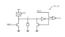
출력드라이버(output driver)는 반도체 메모리장치에서 데이터를 출력하는 곳으로 도면과 같이, 업/다운에 구비된 프리드라이버(pre-driver)(210, 220)와 데이터를 출력하기 위한 풀업 터미네이션 저항부(230)와 풀다운 터미네이션 저항부(240)를 포함하여 구성된다.The output driver outputs data from the semiconductor memory device, and as shown in the figure, pre-drivers 210 and 220 provided for up / down and pull-up termination resistors for outputting data ( 230 and a pull-
그 동작을 간략히 보면, 업/다운에 구비된 프리드라이버(210, 220)는 풀업 터미네이션 저항부(230)와 풀다운 터미네이션 저항부(240)를 각각 제어하는데, '하이'데이터를 출력할 때는 풀업 터미네이션 저항부(230)가 턴온되어 데이터 핀(DQ)을 '하이'상태로 만들고, '로우'데이터를 출력할 때는 풀다운 터미네이션 저항부(240)가 턴온되어 데이터 핀(DQ)을 '로우' 상태로 만든다. 즉, 풀업 또는 풀다운으로 터미네이션을 시켜서 '하이'또는 '로우'의 데이터를 출력한다.In brief, the pre-drivers 210 and 220 provided in the up / down control the pull-
이때 턴온되는 풀업 터미네이션 저항부(230)와 풀다운 터미네이션 저항부(240) 내의 저항의 갯수는 풀업 캘리브래이션 코드(PCODE<0:N>)와 풀다운 캘리브래이션 코드(NCODE<0:N>)에 의해 결정된다. 즉, 풀업 터미네이션 저항부(230)를 턴온하는지 풀다운 터미네이션 저항부(240)를 턴온하는지의 여부는 출력하는 데이터의 논리상태에 따라 결정되지만, 턴온되는 터미네이션 저항부(230, 240) 내의 저항 하나하나의 온/오프는 캘리브래이션 코드(PCODE<0:N>, NCODE<0:N>)에 의해 결정된 다.At this time, the number of resistors in the pull-
참고로, 풀업 터미네이션 저항부(230)와 풀다운 터미네이션 저항부(230)의 타겟(target) 값은 반드시 캘리브래이션 저항부(도 1의 110, 120, 130)의 저항값(240Ω)과 동일한 것이 아니라 240Ω의 1/2 또는 1/4인 120Ω, 60Ω 등의 값을 가질 수도 있다. 도면의 프리드라이버(210, 220)로 입력되는 DQp_CTRL, DQn_CTRL은 프리드라이버(210, 220)로 입력되는 여러 제어신호들을 묶어서 나타낸 것이다.For reference, the target value of the pull-
상술한 온 다이 터미네이션 장치의 ZQ캘리브래이션 동작은 캘리브래이션 저항들(도 1의 110, 120, 130)과 터미네이션 저항들(230. 240) 간에 미스매치(mismatch)가 없고 일정비로 저항값을 크게하거나 작게 할 수 있다는 가정에 근거한다.The ZQ calibration operation of the on-die termination device described above has no mismatch between the calibration resistors (110, 120, and 130 of FIG. 1) and the
그러나 프로세스 오차(process variation) 등에 의해 각 저항들간에 미스매치가 존재하며, 캘리브래이션 회로 내의 비교기의 오프셋, 전원전압의 노이즈(noise), 라인로딩(line loading), 패드(pad) 및 패키지(package) 저항 등 여러 요인에 의해 터미네이션 저항은 목표값을 가지지 못하게 될 수 있다. 터미네이션 저항이 본래 목표로 하는 저항값을 갖지 못하면 입/출력 데이터의 왜곡이 발생할 수 있다. 따라서 이러한 오차를 보정하는 것이 가능한 온 다이 터미네이션 장치가 요구된다.However, there is a mismatch between the resistors due to process variation, etc., and the offset of the comparator in the calibration circuit, the noise of the supply voltage, the line loading, the pad and the package ( Package resistance may cause termination resistors to have no target value. If the termination resistors do not have the desired resistance value, distortion of the input / output data may occur. Accordingly, there is a need for an on die termination device capable of correcting such errors.
본 발명은 상술한 종래기술의 문제점을 해결하기 위하여 제안된 것으로, 온 다이 터미네이션 장치의 캘리브래이션 회로에서 생성된 캘리브래이션 코드에 변경을 가해 온 다이 터미네이션 장치의 오차를 보정 하는데 그 목적이 있다.The present invention has been proposed to solve the above-mentioned problems of the prior art, and has an object of correcting an error of a die termination device that has been changed by a calibration code generated in a calibration circuit of an on die termination device. .
상기한 목적을 달성하기 위한 본 발명의 일실시예에 따른 온 다이 터미네이션 장치의 캘리브래이션 회로는, 제1노드의 전압과 기준전압에 응답하여 터미네이션 저항값의 결정을 위한 캘리브래이션 코드를 생성하는 코드생성부; 상기 캘리브래이션 코드에 응답하여 내부의 저항들이 온/오프 되며, 상기 제1노드에 연결된 캘리브래이션 저항부; 및 상기 캘리브래이션 저항부에 병렬로 연결되어 셋팅값에 따라 변하는 저항값을 갖는 가변저항부를 포함한다.The calibration circuit of the on-die termination device according to an embodiment of the present invention for achieving the above object, generates a calibration code for determining the termination resistance value in response to the voltage and the reference voltage of the first node. Code generation unit to; Internal resistances are turned on / off in response to the calibration code, and a calibration resistor connected to the first node; And a variable resistor unit connected in parallel to the calibration resistor unit and having a resistance value that varies according to a setting value.
또한, 본 발명의 다른 실시예에 따른 온 다이 터미네이션 장치의 캘리브래이션 회로는, 제1노드의 전압과 기준전압에 응답하여 제1캘리브래이션 코드를 제2노드의 전압과 기준전압에 응답하여 제2캘리브래이션 코드를 생성하는 코드생성부; 상기 제1캘리브래이션 코드에 응답하여 내부의 저항들이 온/오프되며, 상기 제1노드에 연결된 제1캘리브래이션 저항부; 상기 제1캘리브래이션 저항부에 병렬로 연결되어 셋팅값에 따라 변하는 저항값을 갖는 제1가변저항부; 상기 제2캘리브래이션 코드에 응답하여 내부의 저항들이 온/오프되며, 상기 제2노드에 연결된 제2캘리브 래이션 저항부; 및 상기 제2캘리브래이션 저항부에 병렬로 연결되어 셋팅값에 따라 변하는 저항값을 갖는 제2가변저항부를 포함한다.In addition, the calibration circuit of the on-die termination device according to another embodiment of the present invention, the first calibration code in response to the voltage and the reference voltage of the first node in response to the voltage and the reference voltage of the second node; A code generator for generating a second calibration code; A first calibration resistor unit configured to turn on / off internal resistances in response to the first calibration code and to be connected to the first node; A first variable resistor unit connected in parallel to the first calibration resistor unit and having a resistance value varying according to a setting value; A second calibration resistor unit configured to turn on / off internal resistors in response to the second calibration code and to be connected to the second node; And a second variable resistor unit connected in parallel to the second calibration resistor unit and having a resistance value that varies according to a setting value.
즉, 셋팅값에 따라 가변저항부의 저항값을 변경함으로서 온 다이 터미네이션 장치의 오차를 보정한다.That is, the error of the on-die termination device is corrected by changing the resistance value of the variable resistor unit according to the setting value.
본 발명은, 가변저항부의 셋팅값을 변경함으로써 캘리브래이션 코드를 쉽게 변경 가능하게 해준다. 따라서 온 다이 터미네이션 장치의 목표 저항값과 실제 터미네이션 저항값 사이에 오차가 발생한 경우 이를 쉽게 보정할 수 있다는 장점이 있다.The present invention makes it possible to easily change the calibration code by changing the setting value of the variable resistor section. Therefore, when an error occurs between the target resistance value of the on-die termination device and the actual termination resistance value, it can be easily corrected.
따라서 임피던스 미스매칭에 의한 데이터 왜곡 등의 현상을 쉽게 방지하는 것이 가능하다는 효과가 있다.Therefore, there is an effect that it is possible to easily prevent phenomena such as data distortion due to impedance mismatching.
이하 본 발명이 속하는 기술 분야에서 통상의 지식을 가진 자가 본 발명의 기술적 사상을 용이하게 실시할 수 있도록 상세히 설명하기 위하여, 본 발명의 가장 바람직한 실시예를 첨부 도면을 참조하여 설명하기로 한다.DETAILED DESCRIPTION Hereinafter, the most preferred embodiments of the present invention will be described with reference to the accompanying drawings so that those skilled in the art may easily implement the technical idea of the present invention.
도 3은 본 발명의 일실시예에 따른 온 다이 터미네이션 장치의 캘리브래이션 회로 구성도이다.3 is a configuration diagram of a calibration circuit of an on die termination apparatus according to an embodiment of the present invention.
도 3의 실시예는 캘리브래이션 회로가 하나의 캘리브래이션 코드를 생성하는 경우를 도시한 것으로 이러한 경우, 캘리브래이션 회로는, 제1노드(ZQ)의 전압과 기준전압(VREF: 일반적으로 1/2 VDDQ)에 응답하여 터미네이션 저항값의 결정을 위한 캘리브래이션 코드(PCODE<0:N>)를 생성하는 코드생성부(310); 캘리브래이션 코드(PCODE<0:N>)에 응답하여 내부의 저항들이 온/오프 되며, 제1노드(ZQ)에 연결된 캘리브래이션 저항부(320); 및 캘리브래이션 저항부(320)에 병렬로 연결되어 셋팅(setting)값에 따라 변하는 저항값을 갖는 가변저항부(330)를 포함하여 구성된다.3 illustrates a case in which a calibration circuit generates one calibration code. In this case, the calibration circuit may include a voltage and a reference voltage VREF of the first node ZQ. A
코드생성부(310)는 종래와 마찬가지로 제1노드(ZQ)의 전압과 기준전압(VREF)을 비교하는 비교기(311)와 비교기(311)의 비교결과에 따라 캘리브래이션 코드(PCODE<0:N>)를 카운팅하는 카운터(312)를 포함하여 구성될 수 있다. 또한, 캘리브래이션 저항부(320)도 종래와 마찬가지로 캘리브래이션 코드(PCODE<0:N>)에 따라 온/오프되며 제1노드(ZQ)의 전압을 변화시킨다.The
가변저항부(330)는 본 발명에서 새로 추가된 부분으로 캘리브래이션 저항부(320)에 병렬로 연결되며, 셋팅값에 따라 자신의 저항값이 결정된다. 캘리브래이션 동작은 제1노드(ZQ)의 전압이 기준전압(VREF)과 같아지도록 캘리브래이션 코드(PCODE<0:N>)를 생성하는 동작이며, 종래에는 캘리브래이션 동작이 끝나면 캘리브래이션 저항부(320)의 저항값=외부저항(301)의 저항값이 되었다.The
그러나 본 발명에서는 가변저항부(330)가 추가되었기 때문에, 캘리브래이션 동작이 끝나면 캘리브래이션 저항부(320)의 저항값+가변저항부의 저항값(330)(병렬 저항의 합을 의미)=외부저항(301)의 저항값이 된다. 따라서 캘리브래이션 코 드(PCODE<0:N>)도 가변저항부(330)가 없을 때와는 다르게 생성되게 된다. 이는 가변저항부(330)의 저항값을 변경함으로써 캘리브래이션 코드(PCODE<0:N>)에 변경을 가할 수 있게 된다는 것을 의미하며, 이를 통해 온 다이 터미네이션 장치의 오차를 보정할 수 있게 된다.However, in the present invention, since the
가변저항부(330)는 퓨즈의 컷팅 여부에 응답하여 신호를 출력하는 하나 이상의 퓨즈회로(331)와, 퓨즈회로(331)의 출력신호에 응답하여 온/오프되는 하나 이상의 저항(332)을 포함하여 구성될 수 있다. 기본적으로 가변저항부(330)의 셋팅값은 퓨즈의 컷팅여부에 의해 결정되며, 테스트모드 신호(TM_UP)에 응답하여 결정되게 할 수도 있다. 퓨즈는 일단 컷팅하면 다시 되돌리는 것이 불가능하기 때문에 먼저 테스트모드 신호(TM_UP)를 인가하여 셋팅값을 적용해 보고, 알맞은 셋팅값이 정해진 후 퓨즈를 컷팅하는 것이 바람직하다. 퓨즈회로(331)와 저항(332)의 갯수는 설계에 따라 변경될 수 있다. 퓨즈회로(331)와 저항(332)을 하나씩만 구비하더라도 온 다이 터미네이션 장치의 오차를 보정하는 것은 가능하지만, 퓨즈회로(331)와 저항(332)의 갯수가 늘어날수록 가변저항부(330)의 저항값을 미세히게 조정하는 것이 가능하다. 퓨즈회로(331)에 대한 보다 상세한 설명은 후술하기로 한다.The
도 3에서는 캘리브래이션 회로가 생성하는 캘리브래이션 코드로 풀업 캘리브래이션 코드(PCODE<0:N>)를 예시하고 있다. 도 3과 같이 캘리브래이션 회로가 하나의 캘리브래이션 코드를 생성하는 경우, 생성되는 캘리브래이션 코드는 항상 풀업 캘리브래이션 코드(PCODE<0:N>)인 것이 아니며, 풀다운 캘리브래이션 코드(NCODE<0:N>)일 수도 있다. 그리고 그런 경우에는 도 3과 달리 외부저항(301)이 풀업저항으로서 연결되어야 할 것이고, 캘리브래이션 저항부(320)와 가변저항부(330)는 풀다운 저항으로 구성되어야 할 것이다.In FIG. 3, a pull-up calibration code PCODE <0: N> is illustrated as a calibration code generated by a calibration circuit. When the calibration circuit generates one calibration code as shown in FIG. 3, the generated calibration code is not always a pull-up calibration code (PCODE <0: N>), but a pull-down calibration code. (NCODE <0: N>). In this case, unlike in FIG. 3, the external resistor 301 should be connected as a pull-up resistor, and the
도 4는 본 발명의 다른 실시예에 따른 온 다이 터미네이션 장치의 캘리브래이션 회로의 구성도이다.4 is a configuration diagram of a calibration circuit of an on die termination device according to another embodiment of the present invention.
도 4의 실시예는 캘리브래이션 회로가 두 개의 캘리브래이션 코드(PCODE<0:N>, NCODE<0:N>)를 생성하는 경우를 도시한 것으로 이러한 경우, 캘리브래이션 회로는, 제1노드(ZQ)의 전압과 기준전압(VREF)에 응답하여 제1캘리브래이션 코드(PCODE<0:N>)를 제2노드(a)의 전압과 기준전압(VREF)에 응답하여 제2캘리브래이션 코드(NCODE<0:N>)를 생성하는 코드생성부(410); 제1캘리브래이션 코드(PCODE<0:N>)에 응답하여 내부의 저항들이 온/오프되며, 제1노드(ZQ)에 연결된 제1캘리브래이션 저항부(420); 제1캘리브래이션 저항부(420)에 병렬로 연결되어 셋팅값에 따라 변하는 저항값을 갖는 제1가변저항부(430); 제2캘리브래이션 코드(NCODE<0:N>)에 응답하여 내부의 저항들이 온/오프되며, 제2노드(a)에 연결된 제2캘리브래이션 저항부(450); 및 제2캘리브래이션 저항부(450)에 병렬로 연결되어 셋팅값에 따라 변하는 저항값을 갖는 제2가변저항부(460)를 포함하여 구성된다. 그리고 제1캘리브래이션 코드(PCODE<0:N>)를 바탕으로 제2캘리브래이션 코드(NCODE<0:N>)를 생성할 수 있게 하는, 제1캘리브래이션 저항부(430)와 동일하게 구성된 더미 캘리브래이션 저항부(440)를 더 포함한다.4 illustrates a case in which the calibration circuit generates two calibration codes PCODE <0: N> and NCODE <0: N>. In this case, the calibration circuit may be configured as follows. In response to the voltage of the first node ZQ and the reference voltage VREF, the first calibration code PCODE <0: N> is converted into a second voltage in response to the voltage and the reference voltage VREF of the second node a. A
코드생성부(410)는 종래의 코드생성부와 마찬가지로, 제1노드(ZQ)의 전압과 기준전압(VREF)을 비교하는 제1비교기(411); 제1비교기(411)의 비교결과에 응답하 여 제1캘리브래이션 코드(PCODE<0:N>)를 카운팅하는 제1카운터412); 제2노드(a)의 전압과 기준전압(VREF)을 비교하는 제2비교기(413); 및 제2비교기(413)의 비교결과에 응답하여 제2캘리브래이션 코드(NCODE<0:N>)를 카운팅하는 제2카운터(414)를 포함하여 구성될 수 있다.The
제1캘리브래이션 저항부(420), 더미 캘리브래이션 저항부(440), 제2캘리브래이션 저항부(450) 역시 종래와 마찬가지로 각각 자신에 해당하는 캘리브래이션 코드(PCODE<0:N>, NCODE<0:N>)를 입력받아 제1노드(ZQ) 또는 제2노드(a)의 전압을 변화시킨다.The first
제1가변저항부(430)는 도 3의 가변저항부(330)와 동일하게, 퓨즈의 컷팅 여부에 응답하여 신호를 출력하는 하나 이상의 퓨즈회로(431)와, 퓨즈회로(431)의 출력신호에 응답하여 온/오프되는 하나 이상의 저항(432)을 포함하여 구성될 수 있다. 따라서 기본적으로 가변저항부(430)의 셋팅값은 퓨즈의 컷팅여부에 의해 결정되며, 테스트모드 신호(TM_UP)에 응답하여 결정되게 할 수도 있다. 퓨즈는 일단 컷팅하면 다시 되돌리는 것이 불가능하기 때문에 먼저 테스트모드 신호(TM_UP)를 인가하여 셋팅값을 적용해 보고, 알맞은 셋팅값이 정해진 후 퓨즈를 컷팅하는 것이 바람직하다. 이러한 제1가변저항부(430)의 저항값을 퓨즈 또는 테스트모드 신호(TM_UP)에 의해 변경시킴으로서 제1캘리브래이션 코드(PCODE<0:N>)를 변경시키는 것이 가능하며, 이러한 변경으로 온 다이 터미네이션 장치의 오차를 보정할 수 있다.The first
제2가변저항부(460) 역시 제1가변저항부(430)와 마찬가지로 퓨즈의 컷팅 여 부에 응답하여 신호를 출력하는 하나 이상의 퓨즈회로(461)와, 퓨즈회로(461)의 출력신호에 응답하여 온/오프되는 하나 이상의 저항(462)을 포함하여 구성될 수 있다. 다만, 제2가변저항부(460) 내의 저항은 제1가변저항부(430) 내의 저항과는 달리 게이트에 퓨즈회로(461)의 출력신호를 인가받는 NMOS트랜지스터의 제어를 받아 온/오프되므로 신호의 극성만 제1가변저항부(430)와 반대로 되게 설계하면 된다.Like the first
제2가변저항부(460)의 저항값 역시 내부의 퓨즈 또는 테스트모드 신호(TM_DN)에 변경하는 것이 가능하다. 제2가변저항부(460)의 저항값을 변경함으로서 제2캘리브래이션 코드(NCODE<0:N>)를 변경시키는 것이 가능하며 이러한 변경으로 온 다이 터미네이션 장치의 오차를 보정할 수 있다.The resistance value of the second
비록 도면에는 제1캘리브래이션 코드는 풀업 캘리브래이션 코드(PCODE<0:N>)로 도시되어 있고, 제2캘리브래이션 코드는 풀다운 캘리브래이션 코드(NCODE<0:N>)로 도시되어 있지만, 이는 서로 바뀔 수가 있다. 예를 들어 제1캘리브래이션 코드가 풀다운 캘리브래이션 코드(NCODE<0:N>)이고 제2캘리브래이션 코드가 풀업 캘리브래이션 코드(PCODE<0:N>)인 경우, 도면과 달리 외부저항(401)은 풀업저항으로, 제1캘리브래이션 저항부(420)와 제1가변저항부(430)와 더미 캘리브래이션 저항부(440)는 풀다운저항으로, 제2캘리브래이션 저항부(450)와 제2가변저항부(460)는 풀업저항으로 변경하여 설계하면 된다. 그러면 외부저항(401)과 캘리브래이션 되면서 제1캘리브래이션 코드가 되는 풀다운 캘리브래이션 코드(NCODE<0:N>)가 먼저 생성되고, 이를 바탕으로 제2캘리브래이션 코드가 되는 풀업 캘리브래이션 코드(PCODE<0:N>)가 생성될 수 있다.Although the first calibration code is shown in the figure as a pull-up calibration code (PCODE <0: N>), the second calibration code is shown as a pull-down calibration code (NCODE <0: N>). But they can be interchanged. For example, if the first calibration code is a pull-down calibration code (NCODE <0: N>) and the second calibration code is a pull-up calibration code (PCODE <0: N>), unlike the drawing The
도 5는 도 3의 가변저항부(330)와 도 4의 제1가변저항부(430)의 퓨즈회로(331, 431)의 일실시예 구성도이다.FIG. 5 is a configuration diagram of
도면의 PWRUPb는 파워업 신호를 나타내며, 전원전압이 안정화되기 전까지는 '하이'레벨을 유지하다 전원전압이 안정화되면 '로우'레벨로 떨어지는 신호이다.PWRUPb in the figure indicates a power-up signal, which is maintained at a 'high' level until the power supply voltage is stabilized, and falls to a 'low' level when the power supply voltage is stabilized.
먼저 테스트모드 신호(TM_UP)가 디스에이블 되었을 때의 동작을 본다. 퓨즈(501)가 컷팅되지 않으면 A노드가 '하이'레벨을 유지하기 때문에 퓨즈회로에서 '하이'신호가 출력되어 저항(332, 432)을 오프시킨다. 그러나 퓨즈(501)가 컷팅되는 경우 A노드는 '하이'레벨을 유지하지 못하고 파워업 신호(PWRUPb)에 의해 '로우'레벨로 떨어지고 퓨즈회로에서는 '로우'신호가 출력되어 저항(332, 432)을 온 시킨다.First, the operation when the test mode signal TM_UP is disabled is described. If the
테스트모드 신호(TM_UP)가 인에이블 되는 경우, 퓨즈회로(331.431)는 퓨즈(501)의 컷팅 여부와 상관없이 항상 '로우'신호를 출력하여 저항(332, 432)을 온 시킨다. 상술한 바와 같이, 테스트모드 신호(TM_UP)는 퓨즈의 컷팅 이전에 세팅값을 적용해 보기 위해 사용될 수 있다.When the test mode signal TM_UP is enabled, the fuse circuit 331.431 always outputs a 'low' signal regardless of whether the
도 6은 도 4의 제2가변저항부(460)의 퓨즈회로(461)의 일실시예 구성도이다.FIG. 6 is a diagram illustrating an embodiment of a
기본적으로 도 5의 퓨즈회로와 동일하지만 퓨즈회로의 출력단에 인버터가 하나 추가되었다. 따라서 동일 조건일 때, 도 5와는 반대 극성의 신호를 출력하게 된다. 이는 도 5의 퓨즈회로(331, 431)의 출력신호는 PMOS트랜지스터의 게이트로 입력되지만, 도 6의 퓨즈회로(461)의 출력신호는 NMOS트랜지스터의 게이트로 입력되기 때문이다.It is basically the same as the fuse circuit of FIG. 5, but an inverter is added to the output terminal of the fuse circuit. Therefore, under the same condition, a signal having a polarity opposite to that of FIG. 5 is output. This is because output signals of the
본 발명의 기술사상은 상기 바람직한 일실시예에 따라 구체적으로 기술되었으나, 상기한 실시예는 그 설명을 위한 것이며 그 제한을 위한 것이 아님을 주의하여야 한다. 또한, 본 발명의 기술분야의 통상의 전문가라면 본 발명의 기술사상의 범위 내에서 다양한 실시예가 가능함을 알 수 있을 것이다.Although the technical spirit of the present invention has been described in detail according to the above preferred embodiment, it should be noted that the above-described embodiment is for the purpose of description and not of limitation. In addition, those skilled in the art will appreciate that various embodiments are possible within the scope of the technical idea of the present invention.
도 1은 종래의 온 다이 터미네이션 장치에서 ZQ캘리브래이션 동작을 수행하는 캘리브래이션 회로의 구성도.1 is a configuration diagram of a calibration circuit for performing a ZQ calibration operation in a conventional on-die termination device.
도 2는 온 다이 터미네이션 장치가 반도체 메모리장치에 적용된 예를 도시한 도면.2 illustrates an example in which an on die termination device is applied to a semiconductor memory device.
도 3은 본 발명의 일실시예에 따른 온 다이 터미네이션 장치의 캘리브래이션 회로 구성도.3 is a configuration diagram of a calibration circuit of an on die termination device according to an embodiment of the present invention.
도 4는 본 발명의 다른 실시예에 따른 온 다이 터미네이션 장치의 캘리브래이션 회로의 구성도.4 is a configuration diagram of a calibration circuit of an on die termination device according to another embodiment of the present invention.
도 5는 도 3의 가변저항부(330)와 도 4의 제1가변저항부(430)의 퓨즈회로(331, 431)의 일실시예 구성도.FIG. 5 is a diagram illustrating an embodiment of
도 6은 도 4의 제2가변저항부(460)의 퓨즈회로(461)의 일실시예 구성도.FIG. 6 is a diagram illustrating an embodiment of a
*도면의 주요 부분에 대한 부호의 설명* Explanation of symbols for the main parts of the drawings
310: 코드생성부 320: 캘리브래이션 저항부310: code generation unit 320: calibration resistance unit
330: 가변저항부330: variable resistance unit
Claims (18)
Translated fromKoreanPriority Applications (2)
| Application Number | Priority Date | Filing Date | Title |
|---|---|---|---|
| KR1020070087070AKR100886644B1 (en) | 2007-08-29 | 2007-08-29 | Calibration Circuit with On Die Termination Device |
| US11/967,720US7884637B2 (en) | 2007-08-29 | 2007-12-31 | Calibration circuit and semiconductor memory device with the same |
Applications Claiming Priority (1)
| Application Number | Priority Date | Filing Date | Title |
|---|---|---|---|
| KR1020070087070AKR100886644B1 (en) | 2007-08-29 | 2007-08-29 | Calibration Circuit with On Die Termination Device |
Publications (1)
| Publication Number | Publication Date |
|---|---|
| KR100886644B1true KR100886644B1 (en) | 2009-03-04 |
Family
ID=40407246
Family Applications (1)
| Application Number | Title | Priority Date | Filing Date |
|---|---|---|---|
| KR1020070087070AExpired - Fee RelatedKR100886644B1 (en) | 2007-08-29 | 2007-08-29 | Calibration Circuit with On Die Termination Device |
Country Status (2)
| Country | Link |
|---|---|
| US (1) | US7884637B2 (en) |
| KR (1) | KR100886644B1 (en) |
Cited By (1)
| Publication number | Priority date | Publication date | Assignee | Title |
|---|---|---|---|---|
| KR101839881B1 (en) | 2011-11-08 | 2018-03-20 | 에스케이하이닉스 주식회사 | Circuit for controlling impedance and semiconductor device including the same |
Families Citing this family (10)
| Publication number | Priority date | Publication date | Assignee | Title |
|---|---|---|---|---|
| JP2013085078A (en)* | 2011-10-07 | 2013-05-09 | Elpida Memory Inc | Semiconductor device and semiconductor module having the same |
| US9111603B1 (en) | 2012-02-29 | 2015-08-18 | Altera Corporation | Systems and methods for memory controller reference voltage calibration |
| US20160012587A1 (en)* | 2013-03-06 | 2016-01-14 | Quynh A. Truong | System and method for non-invasive determination of cardiac activation patterns |
| KR102070619B1 (en) | 2013-03-13 | 2020-01-30 | 삼성전자주식회사 | Circuit and method of on-die termination, semiconductor device including the same |
| KR102185284B1 (en) | 2013-12-12 | 2020-12-01 | 삼성전자 주식회사 | Buffer circuit compensating mismatch of on die termination resistors, semiconductor device and operating method thereof |
| KR20170075103A (en)* | 2015-12-22 | 2017-07-03 | 삼성전자주식회사 | Memory module comprising on-die termination circuit and control method thereof |
| KR102679069B1 (en)* | 2016-10-05 | 2024-07-02 | 에스케이하이닉스 주식회사 | Output circuit using a calibration circuit and semiconductor devices and systems including the same |
| KR20190036259A (en)* | 2017-09-27 | 2019-04-04 | 에스케이하이닉스 주식회사 | Transmitting device using calibration circuit, semiconductor apparatus and system including the same |
| CN112953537B (en)* | 2021-02-05 | 2022-02-15 | 中国电子科技集团公司第五十八研究所 | Fuse calibration unit circuit of current steering DAC |
| US12081212B2 (en)* | 2022-11-18 | 2024-09-03 | Nxp Usa, Inc. | Redriver and resistive termination unit for a redriver |
Citations (2)
| Publication number | Priority date | Publication date | Assignee | Title |
|---|---|---|---|---|
| KR20050104236A (en)* | 2004-04-28 | 2005-11-02 | 주식회사 하이닉스반도체 | Device for calibrating the termination voltage of a on die termination |
| KR20070008245A (en)* | 2005-07-13 | 2007-01-17 | 삼성전자주식회사 | How to set low voltage differential signal receiver and its termination resistance |
Family Cites Families (12)
| Publication number | Priority date | Publication date | Assignee | Title |
|---|---|---|---|---|
| US5606275A (en)* | 1995-09-05 | 1997-02-25 | Motorola, Inc. | Buffer circuit having variable output impedance |
| JP3670563B2 (en)* | 2000-09-18 | 2005-07-13 | 株式会社東芝 | Semiconductor device |
| KR100422451B1 (en)* | 2002-05-24 | 2004-03-11 | 삼성전자주식회사 | method for controlling on-die termination and control circuit therefore |
| DE10245536B4 (en) | 2002-09-30 | 2005-02-03 | Infineon Technologies Ag | Calibrating semiconductor devices using a common calibration reference |
| JP2004320231A (en)* | 2003-04-14 | 2004-11-11 | Renesas Technology Corp | Output circuit for semiconductor device |
| US6924660B2 (en) | 2003-09-08 | 2005-08-02 | Rambus Inc. | Calibration methods and circuits for optimized on-die termination |
| US6980020B2 (en) | 2003-12-19 | 2005-12-27 | Rambus Inc. | Calibration methods and circuits for optimized on-die termination |
| KR100604843B1 (en) | 2004-03-26 | 2006-07-31 | 삼성전자주식회사 | Memory module having on-die termination circuit and its control method |
| KR100532972B1 (en) | 2004-04-28 | 2005-12-01 | 주식회사 하이닉스반도체 | On die termination impeadance calibration device |
| KR100670702B1 (en) | 2004-10-30 | 2007-01-17 | 주식회사 하이닉스반도체 | Semiconductor memory device with on-die termination circuit |
| US7268712B1 (en)* | 2006-04-18 | 2007-09-11 | Taiwan Semiconductor Manufacturing Co., Ltd. | System and method for calibrating on-die components |
| US7514954B2 (en)* | 2006-05-10 | 2009-04-07 | Micron Technology, Inc. | Method and apparatus for output driver calibration |
- 2007
- 2007-08-29KRKR1020070087070Apatent/KR100886644B1/ennot_activeExpired - Fee Related
- 2007-12-31USUS11/967,720patent/US7884637B2/enactiveActive
Patent Citations (2)
| Publication number | Priority date | Publication date | Assignee | Title |
|---|---|---|---|---|
| KR20050104236A (en)* | 2004-04-28 | 2005-11-02 | 주식회사 하이닉스반도체 | Device for calibrating the termination voltage of a on die termination |
| KR20070008245A (en)* | 2005-07-13 | 2007-01-17 | 삼성전자주식회사 | How to set low voltage differential signal receiver and its termination resistance |
Cited By (1)
| Publication number | Priority date | Publication date | Assignee | Title |
|---|---|---|---|---|
| KR101839881B1 (en) | 2011-11-08 | 2018-03-20 | 에스케이하이닉스 주식회사 | Circuit for controlling impedance and semiconductor device including the same |
Also Published As
| Publication number | Publication date |
|---|---|
| US20090059704A1 (en) | 2009-03-05 |
| US7884637B2 (en) | 2011-02-08 |
Similar Documents
| Publication | Publication Date | Title |
|---|---|---|
| KR100886644B1 (en) | Calibration Circuit with On Die Termination Device | |
| KR100879783B1 (en) | On die termination device and semiconductor memory device including same | |
| KR100879782B1 (en) | On die termination device and semiconductor memory device including same | |
| KR100853466B1 (en) | On-die termination device and method for speeding up its calibration operation | |
| KR100875673B1 (en) | On-die termination device and its calibration method | |
| KR100904482B1 (en) | Calibration Circuit with On Die Termination Device | |
| KR100780646B1 (en) | An on die termination device and a semiconductor device comprising the same. | |
| US8508251B2 (en) | Semiconductor devices having on-die termination structures for reducing current consumption and termination methods performed in the semiconductor devices | |
| US8120381B2 (en) | Impedance adjusting device | |
| KR100820783B1 (en) | On-die termination with reduced mismatch | |
| US20100007375A1 (en) | Termination resistance circuit | |
| KR100870427B1 (en) | On Die Termination Device | |
| KR20130072042A (en) | Termination circuit | |
| KR100907929B1 (en) | BUUB test apparatus and test method for semiconductor chip | |
| KR20130072056A (en) | Impedance code generating circuit and semiconductor device including the same | |
| KR20090022043A (en) | Calibration Circuit with On Die Termination Device | |
| KR100968419B1 (en) | Parallel resistance circuit and on-die termination device including the same, semiconductor memory device | |
| KR100838366B1 (en) | Calibration circuit of on-die termination device with offset compensation. | |
| KR101175245B1 (en) | Circuit for impedance adjusting and integrarted circuit chip including the same | |
| KR100904466B1 (en) | Termination Circuits for On Die Termination Devices | |
| KR20090023833A (en) | On die termination device | |
| KR20100109143A (en) | Calibration circuit having fast speed |
Legal Events
| Date | Code | Title | Description |
|---|---|---|---|
| A201 | Request for examination | ||
| PA0109 | Patent application | St.27 status event code:A-0-1-A10-A12-nap-PA0109 | |
| PA0201 | Request for examination | St.27 status event code:A-1-2-D10-D11-exm-PA0201 | |
| D13-X000 | Search requested | St.27 status event code:A-1-2-D10-D13-srh-X000 | |
| D14-X000 | Search report completed | St.27 status event code:A-1-2-D10-D14-srh-X000 | |
| E902 | Notification of reason for refusal | ||
| PE0902 | Notice of grounds for rejection | St.27 status event code:A-1-2-D10-D21-exm-PE0902 | |
| P11-X000 | Amendment of application requested | St.27 status event code:A-2-2-P10-P11-nap-X000 | |
| P13-X000 | Application amended | St.27 status event code:A-2-2-P10-P13-nap-X000 | |
| E701 | Decision to grant or registration of patent right | ||
| PE0701 | Decision of registration | St.27 status event code:A-1-2-D10-D22-exm-PE0701 | |
| GRNT | Written decision to grant | ||
| PR0701 | Registration of establishment | St.27 status event code:A-2-4-F10-F11-exm-PR0701 | |
| PR1002 | Payment of registration fee | St.27 status event code:A-2-2-U10-U11-oth-PR1002 Fee payment year number:1 | |
| PG1601 | Publication of registration | St.27 status event code:A-4-4-Q10-Q13-nap-PG1601 | |
| FPAY | Annual fee payment | Payment date:20120126 Year of fee payment:4 | |
| PR1001 | Payment of annual fee | St.27 status event code:A-4-4-U10-U11-oth-PR1001 Fee payment year number:4 | |
| PN2301 | Change of applicant | St.27 status event code:A-5-5-R10-R13-asn-PN2301 St.27 status event code:A-5-5-R10-R11-asn-PN2301 | |
| PN2301 | Change of applicant | St.27 status event code:A-5-5-R10-R13-asn-PN2301 St.27 status event code:A-5-5-R10-R11-asn-PN2301 | |
| LAPS | Lapse due to unpaid annual fee | ||
| PC1903 | Unpaid annual fee | St.27 status event code:A-4-4-U10-U13-oth-PC1903 Not in force date:20130226 Payment event data comment text:Termination Category : DEFAULT_OF_REGISTRATION_FEE | |
| PC1903 | Unpaid annual fee | St.27 status event code:N-4-6-H10-H13-oth-PC1903 Ip right cessation event data comment text:Termination Category : DEFAULT_OF_REGISTRATION_FEE Not in force date:20130226 | |
| PN2301 | Change of applicant | St.27 status event code:A-5-5-R10-R13-asn-PN2301 St.27 status event code:A-5-5-R10-R11-asn-PN2301 |