KR100886308B1 - Imaging systems to increase reading speeds of solid state imagers, how they operate, and holographic memory systems - Google Patents
Imaging systems to increase reading speeds of solid state imagers, how they operate, and holographic memory systemsDownload PDFInfo
- Publication number
- KR100886308B1 KR100886308B1KR1020047002359AKR20047002359AKR100886308B1KR 100886308 B1KR100886308 B1KR 100886308B1KR 1020047002359 AKR1020047002359 AKR 1020047002359AKR 20047002359 AKR20047002359 AKR 20047002359AKR 100886308 B1KR100886308 B1KR 100886308B1
- Authority
- KR
- South Korea
- Prior art keywords
- output
- analog
- circuit
- sample hold
- digital converter
- Prior art date
- Legal status (The legal status is an assumption and is not a legal conclusion. Google has not performed a legal analysis and makes no representation as to the accuracy of the status listed.)
- Expired - Lifetime
Links
Images


Classifications
- H—ELECTRICITY
- H04—ELECTRIC COMMUNICATION TECHNIQUE
- H04N—PICTORIAL COMMUNICATION, e.g. TELEVISION
- H04N25/00—Circuitry of solid-state image sensors [SSIS]; Control thereof
- H04N25/70—SSIS architectures; Circuits associated therewith
- H04N25/76—Addressed sensors, e.g. MOS or CMOS sensors
- H04N25/767—Horizontal readout lines, multiplexers or registers
- H—ELECTRICITY
- H04—ELECTRIC COMMUNICATION TECHNIQUE
- H04N—PICTORIAL COMMUNICATION, e.g. TELEVISION
- H04N25/00—Circuitry of solid-state image sensors [SSIS]; Control thereof
- H04N25/70—SSIS architectures; Circuits associated therewith
- H04N25/76—Addressed sensors, e.g. MOS or CMOS sensors
- H04N25/78—Readout circuits for addressed sensors, e.g. output amplifiers or A/D converters
Landscapes
- Engineering & Computer Science (AREA)
- Multimedia (AREA)
- Signal Processing (AREA)
- Transforming Light Signals Into Electric Signals (AREA)
- Analogue/Digital Conversion (AREA)
- Solid State Image Pick-Up Elements (AREA)
Abstract
Translated fromKoreanDescription
Translated fromKorean본 출원은 2001년 8월 17일자로 출원된 미국 가출원 제60/313,117호의 이익을 청구하고, 가출원의 내용은 그 전체가 여기에 참조용으로 사용된다.This application claims the benefit of US Provisional Application No. 60 / 313,117, filed August 17, 2001, the contents of which are incorporated herein by reference in their entirety.
본 발명은 이미징 시스템들에 관한 것이다. 보다 구제척으로는, 이미징 시스템에서의 고속 아날로그-디지털 변환을 위한 구조에 관한 것이다.The present invention relates to imaging systems. More specifically, it relates to a structure for high speed analog-to-digital conversion in an imaging system.
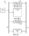
도 1은 CMOS 능동 화소 센서(APS) 이미징 시스템(100)을 도시한 것이다. 시스템(100)은, 도 3에 도시하는 바와 같이 행 디코더(112) 및 N 행들 및 M 열들의 어레이(111)로 배열된 다수의 화소들(P)을 포함하는 화소 어레이(110)를 포함한다. 시스템(100)이 컬러 시스템이라면, 화소들(P)은 적색, 녹색, 청색의 원색에 민감하게 될 것이고, 일반적으로, 교호하는 녹색과 적색 화소들 및 교호하는 청색과 녹색 화소들로, 교호하는 행들이 각각 구성되는 바이어(Bayer) 패턴으로 배열될 것이다.1 illustrates a CMOS active pixel sensor (APS)
도 2는 화소(P)에 대한 하나의 예시적인 구조를 도시한다. 화소(P)는, 광 에너지를 전기 신호로 변환하는 광다이오드(210) 등의 감광 소자를 포함한다. 광다이오드(210)는 노드-A에 접속되고, 이는 또한 트랜지스터(220)의 소스/드레인 단자에 접속된다. 트랜지스터(220)는 Vdd 전원에 접속되는 다른 소스/드레인 단자 및 독출 신호를 수신하도록 접속된 게이트를 갖는다. 노드-A는 소스 팔로잉 트랜지스터(230)의 게이트에 접속되고, 이 트랜지스터는 Vdd 전원에 접속되는 하나의 소스/드레인 단자 및 행 트랜지스터(240)의 소스/드레인 단자에 접속되는 다른 소스/드레인 단자를 갖는다. 행 트랜지스터(240)는 그 게이트를 ROW 제어 신호에 접속시키고, 그 다른 소스/드레인 단자를 노드-B에서 출력 라인(250)에 접속시킨다.2 shows one exemplary structure for the pixel P. As shown in FIG. The pixel P includes a photosensitive element such as a
화소(P)는 감광 소자(210)가 감지한 광의 휘도에 관련된 전압을 노드-A에 생성한다. 노드-A의 전압은 소스 팔로잉 트랜지스터(230)의 게이트를 제어하여 노드-B에서의 출력을 제어한다. 행 트랜지스터(240)는 소스 팔로워 트랜지스터(230)의 출력이 노드-B에서의 출력 라인(250)에 접속되는지의 여부를 라인(260) 상의 ROW 신호를 통해 제어한다. 출력 라인(250)은, 어레이의 열 위치는 동일하지만 상이한 행에 속하는 어레이(110)의 다른 화소들(P)에 또한 접속된다. 도시한 화소(P)는 단지 하나의 예시적인 화소 구조라는 것에 유념해야 한다. 공지된 바와 같이, 예를 들어 리셋 트랜지스터들을 이용하고, 광 신호 요소와 리셋 신호 요소를 구비하는 차분 신호를 출력하는 것들을 포함해서, 화소들에 대해 적합한 몇몇의 서로 다른 구조들이 존재한다.The pixel P generates a voltage related to the brightness of light sensed by the
다시 도 1을 참조하면, 화소(P)에 의한 전기 신호 출력은 아날로그 신호들이다. 이어서, 이들 신호는 아날로그 처리 및 디지털화 회로(저부)(120b) 또는 아날로그 처리 및 디지털화 회로(상부)(120t) 중 하나에 의해 처리되고 디지털화된다. 회로들(120b, 120t)은, 디지털 영역에서 또다른 처리(예를 들어, 컬러 보간) 및 기억을 위하여, 아날로그 신호를 동등한 디지털 신호로 변환하여 이 디지털 신호를 데이터 버스(181)를 통해 디지털 처리 및 기억 시스템(130)으로 이송한다. 제어 회로(140)는 제어 버스(182)를 통해 화소 어레이(110), 아날로그 처리 및 디지털화 시스템(120b, 120t), 그리고 디지털 처리 및 기억 시스템(140)의 동작을 조정한다.Referring back to FIG. 1, the electrical signal output by the pixel P is analog signals. These signals are then processed and digitized by either analog processing and digitization circuit (bottom) 120b or analog processing and digitization circuit (top) 120t.
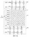
도 3은 화소 어레이(110)와 아날로그 처리 및 디지털화 시스템들(120b, 120t)의 보다 상세한 도면이다. 화소 어레이(110)는 화소들(P)의 어레이(111) 및 행 디코더(112)를 포함한다. 행 디코더(112)는 예를 들어 신호 라인(113) 상의 제어 회로(140)로부터 행 어드레스를 수신한다. 행 디코더(112)는 행 어드레스를 복호하고, 신호 라인(260) 중 하나를 하이 논리 상태로 구동하면서, 다른 신호 라인들(260)은 로우 논리 상태로 유지함으로써 어레이(111)의 하나의 행을 활성화시킨다.3 is a more detailed view of
아날로그 처리 및 디지털화 회로(120b, 120t) 각각은 다수의 샘플 홀드 회로들(121) 및 아날로그-디지털 변환기들(123)을 포함한다. 샘플 홀드 회로들(121)은화소 어레이의 각 열 출력 라인(250)에 각각 접속된다. 보다 상세하게는, 저부의 아날로그 처리 및 디지털화 회로(120b)의 샘플 홀드 회로들(121)은 라인들(250)을 통해 홀수 번호 열들에 접속되고, 상부의 아날로그 처리 및 디지털화 회로(120t)의 샘플 홀드 회로들(121)은 라인들(250)을 통해 짝수 번호 열들에 접속된다. 샘플 홀드 회로들(121) 각각은 제어 신호들(SHEb 및 SHEt)을 각각 수신하기 위해 신호 라인(122b)(저부의 아날로그 처리 및 디지털화 회로(120b)용) 또는 신호 라인(122t)(상부의 아날로그 처리 및 디지털화 회로(120t)용)에 또한 접속된다. 제어 신호(SHEb 및 SHEt)의 상태는 샘플 홀드 회로들(121)이 그 입력 신호들을 샘 플링하고 유지하는 때를 결정한다.Each of the analog processing and digitizing
샘플 홀드 회로(121)는 각각 대응하는 아날로그-디지털 변환기(123)에 연관된다. 각각의 아날로그-디지털 변환기(123)는 각 샘플 홀드 회로(121)가 출력하는 신호를 그 입력으로서 수취한다. 아날로그-디지털 변환기(123) 각각은, 아날로그 -디지털 변환을 수행할 시기를 결정하기 위해서, 신호 라인(124b)(저부의 아날로그 처리 및 디지털화 회로(120b)용) 또는 신호 라인(124t)(상부의 아날로그 처리 및 디지털화 회로(120t)용) 상에서 제어 신호들(ADEb, ADEt)을 각각 수취한다.The
또한 도 4를 참조하면, 화소 어레이(110), 및 상부와 저부 아날로그 처리 및 디지털화 회로들(120b, 120t)의 동작을 설명할 수 있다. 행 디코더(111)가 신호 라인들(260) 중 하나를 하이 논리 상태로 설정하고 다른 신호 라인들(260)을 로우 논리 상태로 설정함으로써 신호 라인(112)에 이전에 공급된 행 어드레스를 복호할 때, 처리가 개시한다. 이는 도 4에서 ROW 신호가 "행 i"에 대해 하이로 상승하는 것에 의해 반영되어 있다. 도 2를 참조하여 상술한 바와 같이, ROW 신호를 인에이블하면 또한 화소(P)의 출력이 출력 라인(250)에 접속되게 된다. 따라서, 행 i에서 홀수 번호 열들에 해당하는 화소들(P)은 그 출력들이 대응하는 샘플 홀드 회로(121)(저부의 아날로그 처리 및 디지털화 회로(120b)의)에 접속되는 한편, 행 i에서 짝수 번호 열들에 해당하는 화소들(P)은 그 출력들이 대응하는 샘플 홀드 회로들(121)(상부의 아날로그 처리 및 디지털화 회로(120t)의)에 접속된다.4, an operation of the
상부의 아날로그 처리 및 디지털화 회로(120t) 및 저부의 아날로그 처리 및 디지털화 회로(120b)는 협력하여 동시에 단일 행을 처리한다. 로우였던 신호들(SHEb, SHEt)은 ROW 신호가 하이로 감에 따라 동시에 하이로 된다. 이것은 저부의 아날로그 처리 및 디지털화 회로 및 상부의 아날로그 처리 및 디지털화 회로(120b)내 샘플 홀드 회로들(121)이 이들 대응하는 화소 신호들을 샘플링하고 유지하게 한다.The upper analog processing and digitizing
다음에, 신호들(SHEb, SHEt)은 로우로 된다. 이 때, 샘플 홀드 회로들은 화소 출력을 버퍼링하고 있어, 버퍼링된 신호를 아날로그-디지털 변환기(124)가 이용할 수 있게 한다.Next, the signals SHEb and SHEt go low. At this point, the sample hold circuits are buffering the pixel output, making the buffered signal available to the analog-to-digital converter 124.
그 후 바로, 로우였던 ADEb 및 ADEt 신호들은 하이로 된다. 이 때문에 저부의 아날로그 처리 및 디지털화 회로 및 상부의 아날로그 처리 및 디지털화 회로(120b, 120t)내의 아날로그-디지털 변환기들(124)을 인에이블시킨다. 홀수 및 짝수 화소들 모두에 대해 샘플 홀드 회로들(121)에 버퍼링된 신호는 디지털 신호로 변환된다. 다음에, ADEb 및 ADEt 신호들은 다시 로우가 된다.Shortly thereafter, the ADEb and ADEt signals that were low go high. This enables the analog to digital converters 124 in the bottom analog processing and digitization circuits and the top analog processing and
디지털 처리 및 기억 시스템(130)(신호 라인(DATA) 상의 "행 i"에 의해 도 4에 표시된)이 디지털 데이터를 이용할 수 있게 될 때, ROW 신호가 행 i+1에 대해 하이로 가는 것으로 표시한 바와 같이 어레이에서 다음 행(예를 들면, 행 i+1)에 대해 처리가 반복된다. 이 처리는 어레이 내의 각 행이 처리될 때까지 반복된다. 이 때, 어레이(110)내의 각 화소(P)는 처리된 상태에서, 처리는 또다른 이미지 프레임에 대해 반복될 수 있다.When the digital processing and storage system 130 (indicated in FIG. 4 by "row i" on signal line DATA) becomes available, the ROW signal is marked high for row i + 1. As one may do, the process is repeated for the next row in the array (eg, row i + 1). This process is repeated until each row in the array has been processed. At this time, in the state where each pixel P in the
따라서, 상술의 장치 및 방법은 어레이(110)내의 각 화소(P)에 의해 출력된 아날로그 신호를 디지털 처리 및 기억 시스템(130)에 의해 디지털 처리되어 기억될 수 있는 디지털 신호로 변환하는 고속 메커니즘을 제공한다. 그러나, 고속 포토그래피, 슬로 모션 촬영, 또는 홀로그래픽 메모리 시스템으로부터 정보를 불러들이는 것과도 같은 일부 응용은 더 빠른 화소 디지털화를 요구한다. 따라서, 이미징 시스템에서 디지털화를 실시하는 고속 구조가 필요하고 요망된다.Accordingly, the apparatus and method described above provide a high speed mechanism for converting the analog signal output by each pixel P in the
본 발명은 이미징 시스템의 디지털화를 실시하는 고속 구조에 관한 것이다. 본 발명의 시스템에 있어서, 화소 어레이는 상부 및 저부 아날로그 처리 및 디지털화 회로들과 연관된다. 상부의 아날로그 처리 및 디지털화 회로와 저부의 아날로그 처리 및 디지털화 회로는 짝수 및 홀수 화소들 모두에 각각 접속된다. 따라서, 동일 행의 홀수 및 짝수 화소들을 따라 샘플 홀드 및 디지털화 처리를 나누는 대신에, 본 발명에서는, 상부 및 저부들이 파이프라인 방식으로 화소 어레이의 서로 다른 행들에서 각각 작업한다.The present invention relates to a high speed structure for digitizing imaging systems. In the system of the present invention, the pixel array is associated with top and bottom analog processing and digitization circuits. The upper analog processing and digitization circuit and the lower analog processing and digitization circuit are connected to both even and odd pixels, respectively. Thus, instead of dividing the sample hold and digitization process along odd and even pixels of the same row, in the present invention, the top and bottom work in different rows of the pixel array, respectively, in a pipelined manner.
본 발명의 상기 및 다른 이점들 및 특징들은 첨부된 도면을 참조하여 이하의 본 발명의 예시적인 실시 형태의 자세한 설명에 의해 보다 명백해진다.The above and other advantages and features of the present invention will become more apparent from the following detailed description of exemplary embodiments of the present invention with reference to the accompanying drawings.
도 1은 종래 기술의 이미지 처리 시스템의 블록도이다.1 is a block diagram of an image processing system of the prior art.
도 2는 종래 기술의 이미지 처리 시스템에 사용하기 위한 화소의 블록도이다.2 is a block diagram of a pixel for use in a prior art image processing system.
도 3은 화소 어레이 및 아날로그 처리 및 디지털화 시스템의 저부 및 상부 영역들의 상세 블록도이다.3 is a detailed block diagram of the bottom and top regions of a pixel array and an analog processing and digitization system.
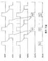
도 4는 도 3에 도시된 장치의 작동을 나타내는 타이밍도이다.4 is a timing diagram illustrating the operation of the apparatus shown in FIG. 3.
도 5는 본 발명에 따른 이미지 처리 시스템의 블록도이다.5 is a block diagram of an image processing system according to the present invention.
도 6은 본 발명의 원리에 따른 화소 어레이와 아날로그 처리 및 디지털화 시스템의 블록도이다.6 is a block diagram of a pixel array and analog processing and digitization system in accordance with the principles of the present invention.
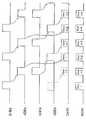
도 7은 도 5에 도시된 장치의 작동을 나타내는 타이밍도이다.FIG. 7 is a timing diagram illustrating operation of the apparatus shown in FIG. 5.
도 8은 본 발명의 원리에 따른 아날로그 처리 및 디지털화 시스템을 사용하는 홀로그래픽 기억 장치의 상세 블록도이다.8 is a detailed block diagram of a holographic memory device using an analog processing and digitization system in accordance with the principles of the present invention.
도 9는 본 발명의 원리에 따른 다른 실시 형태의 상세 블록도이다.9 is a detailed block diagram of another embodiment according to the principles of the present invention.
도면을 참조하여, 동일 요소에는 동일 참조 부호를 지정하여, 도 5에 본 발명의 원리가 반영된 이미징 시스템(500)의 일부를 도시하고 있다. 상기 이미징 시스템은 변형된 상부 및 저부 아날로그 처리 및 디지털화 회로들(120a', 120b')에 접속되는 변형된 화소 어레이(110')를 포함한다. 본 발명의 설명에서는 분리된 회로들을 명시하기 위해서 "상부" 및 "저부"와 같은 용어를 사용하지만, 당업자는 이들 분리된 회로들이 화소 어레이의 상부 및 저부에 물리적으로 위치할 필요는 없고, 이미징 칩 상에 편리한 어느 곳이나 위치할 수 있다는 것을 알 것이다. 상기 이미징 시스템은 디지털 처리 및 기억 시스템(130)을 또한 포함한다. 도 1의 이미징 시스템(100)과 같이, 화소 어레이에서의 화소들은 광을 아날로그 처리 및 디지털화 회로들(120a', 120b')에 의해 디지털화되고, 디지털 처리 및 기억 시스템(130)에 의해 더 처리되어 디지털 도메인에 기억되는 아날로그 전기 신호로 변환한다.Referring to the drawings, like elements are designated by like reference numerals, and a portion of the
도시되는 실시 형태에 있어서, 아날로그 처리 및 디지털화 회로들(120a', 120b')은 데이터 버스(181)를 통하여 디지털 처리 및 기억 시스템에 접속된다. 마찬가지로, 제어기(140)는 제어 버스(182)를 통하여 아날로그 처리 및 디지털화 회로들(120a', 120b'), 화소 어레이(110'), 및 디지털 처리 및 기억 시스템(130)에 접속된다. 그러나, 제어 및 데이터 신호들이 이미징 시스템(500)의 구성 요소 간에 상이하게 전달될 수 있다는 것을 인지하여야 한다. 예를 들면, 분리된 데이터 및 제어 버스들 대신에, 단일 버스가 데이터 및 제어 신호들 모두를 전달하는데 사용될 수도 있다. 또는, 제어 및/또는 데이터 신호들은, 회로간에, 또는 회로로부터 시스템에, 필요에 따라 점 대 점 링크들에 의해 보내질 수 도 있다.In the embodiment shown, analog processing and
도 6에 도시된 바와 같이, 각각의 아날로그 처리 및 디지털화 회로(120a', 120b')는 다수의 샘플 홀드 회로들(121) 및 다수의 아날로그-디지털 변환기들(123)을 포함한다. 샘플 홀드 회로들(121)은 화소의 각각의 열들에 연관된 출력 라인(250)에 각각 접속된다. 본 발명에 있어서, 아날로그 처리 및 디지털화 회로들(120a', 120b') 양쪽의 샘플 홀드 회로들(121)은 어레이(111)의 홀수 및 짝수 번호의 열들 모두에 접속된다. 각 열은 각각의 라인(250)에 의해 열에 접속된 열의 상부(120a') 및 저부(120b') 양쪽에서 샘플 홀드 회로(121)를 또한 갖는다. 각 샘플 홀드 회로(121)는 제어 신호들(SHEa, SHEb) 각각을 수신하는 신호 라인(122b)(회로(120b')용) 또는 신호 라인(122a)(회로(120a')용)에 또한 접속된다. 제어 신호들(SHEa, SHEb)의 상태는 샘플 홀드 회로(121)가 이의 입력 신호를 샘플링하고 유지할 때를 결정한다.As shown in FIG. 6, each analog processing and
각 샘플 홀드 회로(121)는 대응하는 아날로그-디지털 변환기(123)와 연관된다. 각 아날로그-디지털 변환기(123)는 그 입력으로서, 샘플 홀드 회로(121)에 의해 출력된 신호를 받는다. 각 아날로그-디지털 변환기(123)는 신호 라인들(124a)(회로(120a)용) 또는 신호 라인(124b)(회로(120b)용) 상에, 언제 아날로그-디지털 변환을 실시하는지를 결정하는 제어 신호들(ADEa, ADEb) 각각을 받는다.Each
도 6 및 도 7의 타이밍도를 참조하여, 변형된 화소 어레이(110') 및 변형된 아날로그 처리 및 디지털화 회로들(120a', 120b')의 동작에 대해 설명한다. 이전에 신호 라인(112)에 공급된 행 어드레스를 행 디코더(112)가 복호하여, 신호 라인들(260) 중 하나를 하이의 논리 상태로 설정할 때, 처리가 시작된다. 다른 신호 라인들(260)은 또한 로우의 논리 상태로 설정된다. 이는, ROW 신호가 "행 i"에 대해 하이로 되는 것으로 도 6에 반영되어 있다. ROW 신호가 하이로 될 때, 복호화된 행(예를 들면, 행 i)에 있는 화소들로부터의 출력은 출력 라인들(250)에 접속된다. 또한, 로우였던 SHEa 신호는 하이로 된다. SHEb 신호는 로우로 유지된다. 이는, 회로(120a)의 샘플 홀드 회로들(121)이 복호된 행의 모든 화소 신호들을 샘플링하여 유지할 수 있게 한다.Referring to the timing diagrams of FIGS. 6 and 7, the operation of the modified
이후, 제어 회로(140)가 행 디코더(112)에 새로운 행 어드레스를 보내는 때, ROW 신호는 로우의 논리 상태로 다시 전환한다. 행 디코더(112)가 행 어드레스의 복호를 종료할 때, 디코딩된 행(예를 들면, 행 i+1)에 대응하는 신호 라인(260)을 하이로 하고, 다른 신호 라인들(260)을 로우의 논리 상태로 설정한다. 이는, ROW 신호가 "행 i+1"에 대해 하이가 되는 것으로 도 7에 반영되어 있다. ROW 신호가 행 i+1에 대해 하이가 되면, APEa 와 SHEb 신호들은 하이로 된다. APEb 와 SHEa 신호들은 로우를 유지한다. APEa를 하이로 하는 것은, 회로(120a')의 아날로그-디지털 변환기들(123)이 샘플 홀드 회로들(121)(회로(120a')의)에 유지된 아날로그 신호를 디지털 신호로 변환하도록 한다. SHEb를 하이로 하는 것은, 회로(120b)의 샘플 홀드 회로들(121)이 행 i+1의 모든 화소 신호를 샘플링하여 유지하도록 한다.Thereafter, when the
이후, 제어 회로(140)가 또다른 행 어드레스를 행 디코더(112)에 보내는 때, ROW 신호는 로우의 논리 상태로 다시 전환한다. 열 디코더(112)가 열 복호를 종료할 때, 복호화된 행(예를 들면, 행 i+2)에 대응하는 신호 라인(260)을 하이로 하고, 다른 신호 라인들(260)은 로우의 논리 상태로 설정한다. 이는, 도 7에서 "행 i+2"에 대해 하이가 되는 로우 신호에 의해 반영된다. ROW 신호가 행 i+2에 대해 하이가 되면, 회로(120a')의 디지털-아날로그 변환기(123)에 의해 변환된 데이터가 출력된다. 이는, 도 7의 DATA 라인에 있는 행 i 블록에 의해 반영된다. 데이터 출력과 함께, 제어 신호들(SHEa 및 ADEb)은 모두 하이가 된다. 이는, 회로(120a')의 샘플 홀드 회로들(121)이 행 i+2로부터의 화소 신호들을 샘플링하여 유지하도록 한다. 또한, 이는 회로(120b')의 아날로그-디지털 변환기들(123)이 디지털 변환을 수행하도록 한다.Then, when the
이후, 제어 회로(140)가 행 어드레스 디코더(112)에 또다른 행을 보내면, ROW 신호는 로우의 논리 상태로 다시 전환한다. 행 디코더(112)가 행 복호화를 종료하면, 행 i+3에 대해 상술한 바와 같이 신호 라인들(260)을 구동한다. 제어 신 호들(APEa 및 SHEb)은 모두 하이가 되고, 이로써 행 i+3의 샘플링 및 유지와 행 i+1에 대응하는 데이터의 출력을 허용한다.Thereafter, when the
상술한 설명은, 처리가 행 i 부터 개시된 것으로 가정한 것이다. 정상적인 동작에서, 처리는 제1 행부터 개시되어야 한다. 행 i가 제1 행이 아니었고, 이 상태에서 ROW 신호가 행 i에 대해 하이가 될 때, 신호(ADEb)도 하이가 될 것이고, ROW 신호가 행 i+1에 대해 다시 하이가 될 때 행 i-1에 대응하는 데이터가 얻어질 것이다. 도 7에서, 앞서 기술한 사건(event)과 관련된 신호들은 점선으로 나타낸다.The above description assumes that the process has been started from row i. In normal operation, processing should start from the first row. When row i was not the first row and in this state the ROW signal goes high for row i, the signal ADEb will also go high and the row when the ROW signal goes high again for row i + 1 Data corresponding to i-1 will be obtained. In FIG. 7, signals related to the above-described event are indicated by dotted lines.
따라서, 본 발명은 상부 및 저부 아날로그 처리 및 디지털화 회로(120a', 120b')를 변형하여, 홀수 및 짝수 컬럼들 양자로부터 신호들을 수신할 수 있도록 하는 것이다. 처리 스루풋(throughput)은, 두 회로들(120a') 중 하나를 사용하여 화소들(P)의 한 행을 샘플링 및 유지하고, 또다른 회로(120b')는 이전의 샘플링되어 유지된 행에 대해 디지털화를 수행함으로써 두배가 된다. 따라서, 어느 때이든지 하나의 샘플 홀드 회로가 활성화되고, 또한 하나의 아날로그-디지털 변환이 활성화된다. 이러한 파이프라인 접근법은, 이전보다 두배 빨리 동작하는 행 디코더를 필요로 하나, 두배의 속도로 데이터 변환을 할 수 있게 한다.Accordingly, the present invention is to modify the top and bottom analog processing and
상술한 바와 같이, 이러한 고속 변환은 예를 들면, 홀로그래픽 메모리 시스템을 독출하는 등의 다양한 적용에서 사용될 수도 있다. 도 8은, 본 발명의 이미징 시스템(500)이 홀로그래픽 메모리 시스템(800)에 어떻게 사용될 수 있는지를 설명하고 있다. 홀로그래픽 메모리 시스템(800)은, 기준 광 빔(reference light beam; R)을 생성하는 레이저(801)를 포함한다. 기준 빔은, 제어가능한 광학계 경로(802)를 이용하여 포커스되어 포커스된 빔(R')을 형성하게 되고, 이것이 홀로그래픽 기록 매체(803)를 비추게 된다. 홀로그래픽 기록 매체는, 포커스된 빔(R')에 응답하여, 포커스된 빔(R')를 회절된 빔(R'')으로 회절시키고, 회절된 빔은 제2 제어가능한 광학계 경로(804)를 통과하여 빔(R''')을 만들게 되며, 이 빔이 본 발명의 이미징 시스템(500)에 의해 읽혀진다. 제어기(805)는, 레이저(801)의 동작, 제어가능한 광학(802), 홀로그래픽 기록 매체(803)의 포지셔닝, 제2 제어가능한 광학(804)의 동작 및 이미징 시스템(500)을 조정한다.As mentioned above, this fast conversion may be used in various applications, for example, reading a holographic memory system. 8 illustrates how the
본 발명의 원리는, 부가적인 아날로그-디지털 변환기(123)와 샘플 홀드 회로들(121)을 사용하여 아날로그 처리 및 디지털화 회로들(120a', 120b')을 변형함으로써, 훨씬 더 빠른 이미지 시스템을 제작하도록 확장될 수 있다. 예를 들면, 도 9는 변형된 아날로그 처리 및 디지털화 회로(120a'')를 도시한 것이다. 유사하게 변형된 회로(120b')(미도시)와 조합하여 동작되도록 설계된 변형한 회로(120a'')는, 2배의 샘플 홀드 회로들(121)과 2배의 아날로그-디지털 변환기들(123)을 사용하고 있다. 원래의 회로들(121, 123)은, 각각 제어 신호들(SHEa1, ADEa1)에 의해 제어되는 반면, 부가적인 회로들(121, 123)은 각각 제어 신호들(SHEa2, ADEa2)에 의해 제어된다. 행 디코더는 두배의 속도로 동작되고, 두 세트의 회로들(121, 123)은 인터리빙 방식으로 동작된다. 이러한 방식으로, 부가적인 세트의 샘플 홀드 회로들과 아날로그-디지털 변환기들(123)을 이용함으로써, 이미지 시스템의 속도를 2배로 하거나, 더 증가시킬 수 있다(인터리빙된 정도에 기초하여).The principles of the present invention produce an even faster imaging system by modifying the analog processing and
본 발명을 예시적인 실시예와 함께 상세히 설명하였으나, 본 발명이 상술한 실시예에 제한되는 것은 아니다. 본 발명은, 여기에 기재하지 않은 많은 변형, 변경, 대체 또는 균등한 구성을 포함하도록 변경될 수 있으며, 이는 본 발명의 사상 및 범위에 속한다.While the invention has been described in detail in conjunction with exemplary embodiments, the invention is not limited to the embodiments described above. The invention may be modified to include many variations, modifications, substitutions or equivalent constructions not described herein, which fall within the spirit and scope of the invention.
따라서, 본 발명은 상술한 설명 또는 도면에 의해 한정되지 않으며, 첨부한 청구항의 범위에 의해서만 제한된다.Accordingly, the invention is not limited by the foregoing description or drawings, but is only limited by the scope of the appended claims.
Claims (23)
Translated fromKoreanApplications Claiming Priority (3)
| Application Number | Priority Date | Filing Date | Title |
|---|---|---|---|
| US31311701P | 2001-08-17 | 2001-08-17 | |
| US60/313,117 | 2001-08-17 | ||
| PCT/US2002/026061WO2003017648A2 (en) | 2001-08-17 | 2002-08-16 | Doubling of speed in cmos sensor with column-parallel adcs |
Publications (2)
| Publication Number | Publication Date |
|---|---|
| KR20040030972A KR20040030972A (en) | 2004-04-09 |
| KR100886308B1true KR100886308B1 (en) | 2009-03-04 |
Family
ID=23214451
Family Applications (1)
| Application Number | Title | Priority Date | Filing Date |
|---|---|---|---|
| KR1020047002359AExpired - LifetimeKR100886308B1 (en) | 2001-08-17 | 2002-08-16 | Imaging systems to increase reading speeds of solid state imagers, how they operate, and holographic memory systems |
Country Status (6)
| Country | Link |
|---|---|
| US (1) | US7565033B2 (en) |
| EP (1) | EP1428380A2 (en) |
| JP (2) | JP4532899B2 (en) |
| KR (1) | KR100886308B1 (en) |
| CN (2) | CN100480897C (en) |
| WO (1) | WO2003017648A2 (en) |
Families Citing this family (54)
| Publication number | Priority date | Publication date | Assignee | Title |
|---|---|---|---|---|
| US7738013B2 (en)* | 2001-05-29 | 2010-06-15 | Samsung Electronics Co., Ltd. | Systems and methods for power conservation in a CMOS imager |
| AU2002305780A1 (en)* | 2001-05-29 | 2002-12-09 | Transchip, Inc. | Patent application cmos imager for cellular applications and methods of using such |
| US7408443B2 (en)* | 2003-01-13 | 2008-08-05 | Samsung Electronics Co., Ltd. | Circuit and method for reducing fixed pattern noise |
| JP4276879B2 (en) | 2003-04-28 | 2009-06-10 | オリンパス株式会社 | Image sensor |
| US7619669B2 (en)* | 2003-12-29 | 2009-11-17 | Micron Technologies, Inc. | Power savings with multiple readout circuits |
| JP4107269B2 (en)* | 2004-02-23 | 2008-06-25 | ソニー株式会社 | Solid-state imaging device |
| JP2005333265A (en)* | 2004-05-18 | 2005-12-02 | Olympus Corp | Solid-state imaging device and apparatus |
| JP4490740B2 (en) | 2004-06-17 | 2010-06-30 | 株式会社アドバンテスト | Signal reading apparatus and test apparatus |
| US7652703B2 (en)* | 2004-07-12 | 2010-01-26 | Micron Technology, Inc. | Dual panel pixel readout in an imager |
| JP4599258B2 (en)* | 2005-09-16 | 2010-12-15 | 富士フイルム株式会社 | Solid-state image sensor |
| US7659925B2 (en)* | 2005-10-04 | 2010-02-09 | Alexander Krymski | High speed CMOS image sensor circuits with memory readout |
| CN101455070B (en)* | 2006-05-22 | 2014-06-11 | 汤姆森特许公司 | Image sensor and method for reading out pixels of the image sensor |
| US8102442B2 (en)* | 2006-05-23 | 2012-01-24 | Thomson Licensing | Image sensor circuit |
| TWI345910B (en)* | 2006-10-02 | 2011-07-21 | Novatek Microelectronics Corp | Cmos image sensor for high-speed operation |
| US7894662B2 (en)* | 2006-10-11 | 2011-02-22 | Tandent Vision Science, Inc. | Method for using image depth information in identifying illumination fields |
| JP2008131498A (en)* | 2006-11-22 | 2008-06-05 | Matsushita Electric Ind Co Ltd | Video processing device |
| US7488928B2 (en) | 2007-04-20 | 2009-02-10 | Alexander Krymski | Image sensor circuits and methods with multiple readout lines per column of pixel circuits |
| JP4929075B2 (en)* | 2007-06-28 | 2012-05-09 | パナソニック株式会社 | Solid-state imaging device, driving method thereof, and imaging device |
| JP5046787B2 (en) | 2007-08-10 | 2012-10-10 | キヤノン株式会社 | Imaging system |
| US7995124B2 (en)* | 2007-09-14 | 2011-08-09 | Omnivision Technologies, Inc. | Image sensor apparatus and method for improved dynamic range with multiple readout circuit paths |
| JP2009077098A (en)* | 2007-09-20 | 2009-04-09 | Sony Corp | Solid-state imaging device and driving method thereof |
| US7920190B2 (en)* | 2007-10-11 | 2011-04-05 | Aptina Imaging Corporation | Method and apparatus providing column parallel architecture for imagers |
| JP4981623B2 (en)* | 2007-11-01 | 2012-07-25 | キヤノン株式会社 | Solid-state imaging device and driving method thereof, camera and copying machine |
| KR101448918B1 (en)* | 2007-12-18 | 2014-10-15 | 삼성전자주식회사 | CMOS image sensor capable of high-speed output of pixel data |
| US8174603B2 (en)* | 2008-05-01 | 2012-05-08 | Alexander Krymski | Image sensors and methods with antiblooming channels and two side driving of control signals |
| US9019411B2 (en) | 2008-05-01 | 2015-04-28 | Alexander Krymski | Image sensors and methods with pipelined readout |
| US7804438B2 (en)* | 2008-05-02 | 2010-09-28 | Alexander Krymski | Image sensors and dual ramp analog-to-digital converters and methods |
| JP2010098516A (en)* | 2008-10-16 | 2010-04-30 | Sony Corp | Imaging element and control method thereof, and camera |
| JP2010114550A (en)* | 2008-11-05 | 2010-05-20 | Sony Corp | Imaging element, drive method for imaging element and camera |
| CA2763826C (en) | 2009-06-17 | 2020-04-07 | 3Shape A/S | Focus scanning apparatus |
| JP2012049597A (en) | 2010-08-24 | 2012-03-08 | Nikon Corp | Imaging apparatus |
| JP2012049911A (en)* | 2010-08-27 | 2012-03-08 | Canon Inc | Photoelectric conversion device and imaging system |
| DE102010035811B4 (en) | 2010-08-30 | 2024-01-25 | Arnold & Richter Cine Technik Gmbh & Co. Betriebs Kg | Image sensor and method for reading an image sensor |
| KR101678842B1 (en) | 2010-10-22 | 2016-11-23 | 삼성전자주식회사 | Analog to digital converter and image sensor including the same |
| US8730364B2 (en) | 2010-11-09 | 2014-05-20 | Omnivision Technologies, Inc. | Image sensor with pipelined column analog-to-digital converters |
| DE102010051438B4 (en) | 2010-11-15 | 2024-03-14 | Arnold & Richter Cine Technik Gmbh & Co. Betriebs Kg | Image sensor |
| US8723093B2 (en) | 2011-01-10 | 2014-05-13 | Alexander Krymski | Image sensors and methods with shared control lines |
| JP5791571B2 (en) | 2011-08-02 | 2015-10-07 | キヤノン株式会社 | Imaging device and imaging apparatus |
| DE102011120099B4 (en) | 2011-12-02 | 2024-05-29 | Arnold & Richter Cine Technik Gmbh & Co. Betriebs Kg | Image sensor and method for reading an image sensor |
| JP2013121027A (en)* | 2011-12-07 | 2013-06-17 | Sony Corp | Solid-state imaging element, method for driving the same, and camera system |
| JP5414848B2 (en)* | 2012-07-11 | 2014-02-12 | キヤノン株式会社 | Imaging system |
| US9294703B2 (en) | 2012-12-03 | 2016-03-22 | Samsung Electronics Co., Ltd. | Image sensor including data transmission circuit having split bus segments |
| JP2014150444A (en)* | 2013-02-01 | 2014-08-21 | Toshiba Corp | Solid-state imaging device |
| KR101444014B1 (en)* | 2013-03-07 | 2014-09-23 | 주식회사 동부하이텍 | Operating circuit of image sensor and operating method thereof |
| US9369648B2 (en) | 2013-06-18 | 2016-06-14 | Alexander Krymski | Image sensors, methods, and pixels with tri-level biased transfer gates |
| JP6175355B2 (en) | 2013-11-07 | 2017-08-02 | ルネサスエレクトロニクス株式会社 | Solid-state image sensor |
| US9578267B2 (en)* | 2013-12-23 | 2017-02-21 | Alexander Krymski | Cameras and methods with data processing, memories, and an image sensor with multiple data ports |
| US10010387B2 (en) | 2014-02-07 | 2018-07-03 | 3Shape A/S | Detecting tooth shade |
| US9521349B2 (en)* | 2014-06-19 | 2016-12-13 | Rambus Inc. | Image sensor architecture with power saving readout |
| JP6579771B2 (en)* | 2015-03-26 | 2019-09-25 | キヤノン株式会社 | Imaging device |
| JP6646824B2 (en) | 2016-01-22 | 2020-02-14 | パナソニックIpマネジメント株式会社 | Imaging device |
| JP2019140636A (en)* | 2018-02-15 | 2019-08-22 | ソニーセミコンダクタソリューションズ株式会社 | Imaging device |
| JP7322552B2 (en)* | 2019-07-01 | 2023-08-08 | 株式会社リコー | Photoelectric conversion device, line sensor, image reading device, and image forming device |
| KR102820466B1 (en)* | 2019-12-13 | 2025-06-17 | 삼성전자주식회사 | Image senosor, image device having the same, and operating method therof |
Citations (4)
| Publication number | Priority date | Publication date | Assignee | Title |
|---|---|---|---|---|
| JPH11191891A (en) | 1997-12-25 | 1999-07-13 | Canon Inc | Solid-state imaging device and signal reading method of solid-state imaging device |
| US6115065A (en) | 1995-11-07 | 2000-09-05 | California Institute Of Technology | Image sensor producing at least two integration times from each sensing pixel |
| JP2001024954A (en)* | 1999-07-08 | 2001-01-26 | Hamamatsu Photonics Kk | Solid-state image pickup device |
| US6466265B1 (en) | 1998-06-22 | 2002-10-15 | Eastman Kodak Company | Parallel output architectures for CMOS active pixel sensors |
Family Cites Families (20)
| Publication number | Priority date | Publication date | Assignee | Title |
|---|---|---|---|---|
| FR2503502B1 (en)* | 1981-03-31 | 1985-07-05 | Thomson Csf | COLOR IMAGE ANALYSIS DEVICE USING ELECTRICAL LOAD TRANSFER AND TELEVISION CAMERA PROVIDED WITH SUCH A DEVICE |
| JP2532374B2 (en)* | 1985-12-27 | 1996-09-11 | 株式会社日立製作所 | Solid-state imaging device |
| GB2206695A (en) | 1987-06-26 | 1989-01-11 | Ford Motor Co | A liquid level indicating device |
| JP2808648B2 (en)* | 1989-04-10 | 1998-10-08 | キヤノン株式会社 | Imaging device |
| JPH0548460A (en) | 1991-06-05 | 1993-02-26 | Matsushita Electric Ind Co Ltd | A/d converter and sensor using the same and three-dimensional integrated circuit |
| US5229962A (en)* | 1991-06-13 | 1993-07-20 | Yuh Perng Fei | Buffered nondestructive-readout Josephson memory cell with three gates |
| JP3089507B2 (en)* | 1992-02-29 | 2000-09-18 | ソニー株式会社 | Solid-state imaging device and signal charge transfer method |
| JPH09238286A (en)* | 1996-02-29 | 1997-09-09 | Toshiba Corp | Digital optical sensor |
| US5995676A (en)* | 1996-12-26 | 1999-11-30 | Lucent Technologies Inc. | Comparator-based thresholding method for determining data values |
| JPH10224697A (en)* | 1997-02-05 | 1998-08-21 | Nikon Corp | Solid-state imaging device and method of driving solid-state imaging device |
| US6271785B1 (en)* | 1998-04-29 | 2001-08-07 | Texas Instruments Incorporated | CMOS imager with an A/D per pixel convertor |
| JP3730442B2 (en)* | 1999-05-14 | 2006-01-05 | 株式会社東芝 | Solid-state imaging device |
| JP2001016502A (en)* | 1999-06-30 | 2001-01-19 | Toshiba Corp | Solid-state imaging device |
| JP4560152B2 (en)* | 1999-07-08 | 2010-10-13 | 浜松ホトニクス株式会社 | Solid-state imaging device |
| JP2001045378A (en) | 1999-08-04 | 2001-02-16 | Canon Inc | Solid-state imaging device |
| JP3611756B2 (en)* | 1999-08-31 | 2005-01-19 | パイオニア株式会社 | Hologram recording apparatus and method thereof |
| JP4777496B2 (en)* | 2000-02-10 | 2011-09-21 | 富士フイルム株式会社 | Solid-state image sensor |
| JP3990857B2 (en)* | 2000-07-03 | 2007-10-17 | キヤノン株式会社 | Imaging apparatus and imaging system |
| JP3877946B2 (en)* | 2000-08-21 | 2007-02-07 | 独立行政法人科学技術振興機構 | High-speed imaging device |
| JP3549841B2 (en)* | 2001-01-30 | 2004-08-04 | 日本電信電話株式会社 | Data conversion / output device |
- 2002
- 2002-08-16KRKR1020047002359Apatent/KR100886308B1/ennot_activeExpired - Lifetime
- 2002-08-16USUS10/219,771patent/US7565033B2/ennot_activeExpired - Lifetime
- 2002-08-16EPEP02761388Apatent/EP1428380A2/ennot_activeWithdrawn
- 2002-08-16WOPCT/US2002/026061patent/WO2003017648A2/enactiveApplication Filing
- 2002-08-16CNCNB2005101085614Apatent/CN100480897C/ennot_activeExpired - Lifetime
- 2002-08-16JPJP2003521608Apatent/JP4532899B2/ennot_activeExpired - Fee Related
- 2002-08-16CNCNB028202902Apatent/CN1252987C/ennot_activeExpired - Lifetime
- 2007
- 2007-01-31JPJP2007021698Apatent/JP4521411B2/ennot_activeExpired - Fee Related
Patent Citations (4)
| Publication number | Priority date | Publication date | Assignee | Title |
|---|---|---|---|---|
| US6115065A (en) | 1995-11-07 | 2000-09-05 | California Institute Of Technology | Image sensor producing at least two integration times from each sensing pixel |
| JPH11191891A (en) | 1997-12-25 | 1999-07-13 | Canon Inc | Solid-state imaging device and signal reading method of solid-state imaging device |
| US6466265B1 (en) | 1998-06-22 | 2002-10-15 | Eastman Kodak Company | Parallel output architectures for CMOS active pixel sensors |
| JP2001024954A (en)* | 1999-07-08 | 2001-01-26 | Hamamatsu Photonics Kk | Solid-state image pickup device |
Also Published As
| Publication number | Publication date |
|---|---|
| KR20040030972A (en) | 2004-04-09 |
| US20030043089A1 (en) | 2003-03-06 |
| JP2005518688A (en) | 2005-06-23 |
| US7565033B2 (en) | 2009-07-21 |
| CN1746796A (en) | 2006-03-15 |
| WO2003017648A3 (en) | 2003-05-01 |
| EP1428380A2 (en) | 2004-06-16 |
| JP4532899B2 (en) | 2010-08-25 |
| WO2003017648A2 (en) | 2003-02-27 |
| CN1568613A (en) | 2005-01-19 |
| CN1252987C (en) | 2006-04-19 |
| JP4521411B2 (en) | 2010-08-11 |
| CN100480897C (en) | 2009-04-22 |
| JP2007243930A (en) | 2007-09-20 |
Similar Documents
| Publication | Publication Date | Title |
|---|---|---|
| KR100886308B1 (en) | Imaging systems to increase reading speeds of solid state imagers, how they operate, and holographic memory systems | |
| US8149312B2 (en) | CMOS image sensor with shared sensing node | |
| US6507011B2 (en) | Active pixel color linear sensor with line-packed pixel readout | |
| EP0809395A2 (en) | An X-Y addressable CMOS APS with compact pixel pitch | |
| US8054375B2 (en) | Physical quantity detecting device, method of driving the physical quantity detecting device and imaging apparatus | |
| JP4601897B2 (en) | Solid-state imaging device and driving method thereof | |
| JP2000032318A (en) | Image input device | |
| JP4661212B2 (en) | Physical information acquisition method, physical information acquisition device, and semiconductor device | |
| JP4286091B2 (en) | Solid-state imaging device | |
| JP4551588B2 (en) | Imaging apparatus and imaging system | |
| JP4628174B2 (en) | Imaging device, image signal processing apparatus, and imaging apparatus | |
| JP5177198B2 (en) | Physical information acquisition method and physical information acquisition device | |
| JP4499387B2 (en) | Solid-state imaging device | |
| JP4506794B2 (en) | Solid-state imaging device and driving method thereof | |
| JP3162644B2 (en) | Solid-state imaging device | |
| TWI586171B (en) | Image sensor with shared column readout circuis | |
| JP2001274962A (en) | Image reader | |
| JP2006217658A (en) | Solid-state image pickup device and method of driving same | |
| JPH04256279A (en) | image sensor chip | |
| JPS6016760A (en) | Original reading device | |
| JP2004040148A (en) | Solid-state imaging element | |
| JPH057346A (en) | Image pickup device | |
| JPH03133245A (en) | Image sensor chip and photoelectric converter using same |
Legal Events
| Date | Code | Title | Description |
|---|---|---|---|
| PA0105 | International application | Patent event date:20040217 Patent event code:PA01051R01D Comment text:International Patent Application | |
| PG1501 | Laying open of application | ||
| AMND | Amendment | ||
| A201 | Request for examination | ||
| AMND | Amendment | ||
| PA0201 | Request for examination | Patent event code:PA02012R01D Patent event date:20070320 Comment text:Request for Examination of Application | |
| AMND | Amendment | ||
| E902 | Notification of reason for refusal | ||
| PE0902 | Notice of grounds for rejection | Comment text:Notification of reason for refusal Patent event date:20080228 Patent event code:PE09021S01D | |
| AMND | Amendment | ||
| E601 | Decision to refuse application | ||
| PE0601 | Decision on rejection of patent | Patent event date:20080715 Comment text:Decision to Refuse Application Patent event code:PE06012S01D Patent event date:20080228 Comment text:Notification of reason for refusal Patent event code:PE06011S01I | |
| AMND | Amendment | ||
| J201 | Request for trial against refusal decision | ||
| PJ0201 | Trial against decision of rejection | Patent event date:20080807 Comment text:Request for Trial against Decision on Refusal Patent event code:PJ02012R01D Patent event date:20080715 Comment text:Decision to Refuse Application Patent event code:PJ02011S01I Appeal kind category:Appeal against decision to decline refusal Decision date:20090129 Appeal identifier:2008101007842 Request date:20080807 | |
| PB0901 | Examination by re-examination before a trial | Comment text:Amendment to Specification, etc. Patent event date:20080807 Patent event code:PB09011R02I Comment text:Request for Trial against Decision on Refusal Patent event date:20080807 Patent event code:PB09011R01I Comment text:Amendment to Specification, etc. Patent event date:20080428 Patent event code:PB09011R02I Comment text:Amendment to Specification, etc. Patent event date:20080228 Patent event code:PB09011R02I Comment text:Amendment to Specification, etc. Patent event date:20070320 Patent event code:PB09011R02I Comment text:Amendment to Specification, etc. Patent event date:20051102 Patent event code:PB09011R02I | |
| E902 | Notification of reason for refusal | ||
| PE0902 | Notice of grounds for rejection | Comment text:Notification of reason for refusal Patent event date:20081010 Patent event code:PE09021S01D | |
| B701 | Decision to grant | ||
| PB0701 | Decision of registration after re-examination before a trial | Patent event date:20090129 Comment text:Decision to Grant Registration Patent event code:PB07012S01D Patent event date:20080909 Comment text:Transfer of Trial File for Re-examination before a Trial Patent event code:PB07011S01I | |
| GRNT | Written decision to grant | ||
| PR0701 | Registration of establishment | Comment text:Registration of Establishment Patent event date:20090223 Patent event code:PR07011E01D | |
| PR1002 | Payment of registration fee | Payment date:20090223 End annual number:3 Start annual number:1 | |
| PG1601 | Publication of registration | ||
| PR1001 | Payment of annual fee | Payment date:20120207 Start annual number:4 End annual number:4 | |
| FPAY | Annual fee payment | Payment date:20130124 Year of fee payment:5 | |
| PR1001 | Payment of annual fee | Payment date:20130124 Start annual number:5 End annual number:5 | |
| FPAY | Annual fee payment | Payment date:20140127 Year of fee payment:6 | |
| PR1001 | Payment of annual fee | Payment date:20140127 Start annual number:6 End annual number:6 | |
| FPAY | Annual fee payment | Payment date:20150129 Year of fee payment:7 | |
| PR1001 | Payment of annual fee | Payment date:20150129 Start annual number:7 End annual number:7 | |
| FPAY | Annual fee payment | Payment date:20151230 Year of fee payment:8 | |
| PR1001 | Payment of annual fee | Payment date:20151230 Start annual number:8 End annual number:8 | |
| FPAY | Annual fee payment | Payment date:20161229 Year of fee payment:9 | |
| PR1001 | Payment of annual fee | Payment date:20161229 Start annual number:9 End annual number:9 | |
| FPAY | Annual fee payment | Payment date:20180212 Year of fee payment:10 | |
| PR1001 | Payment of annual fee | Payment date:20180212 Start annual number:10 End annual number:10 | |
| FPAY | Annual fee payment | Payment date:20190207 Year of fee payment:11 | |
| PR1001 | Payment of annual fee | Payment date:20190207 Start annual number:11 End annual number:11 | |
| PR1001 | Payment of annual fee | Payment date:20210202 Start annual number:13 End annual number:13 | |
| PR1001 | Payment of annual fee | Payment date:20220125 Start annual number:14 End annual number:14 | |
| PC1801 | Expiration of term | Termination date:20230216 Termination category:Expiration of duration |