KR100883769B1 - Manufacturing method of array substrate for liquid crystal display device - Google Patents
Manufacturing method of array substrate for liquid crystal display deviceDownload PDFInfo
- Publication number
- KR100883769B1 KR100883769B1KR1020020069285AKR20020069285AKR100883769B1KR 100883769 B1KR100883769 B1KR 100883769B1KR 1020020069285 AKR1020020069285 AKR 1020020069285AKR 20020069285 AKR20020069285 AKR 20020069285AKR 100883769 B1KR100883769 B1KR 100883769B1
- Authority
- KR
- South Korea
- Prior art keywords
- layer
- electrode
- copper
- gate
- alloy
- Prior art date
- Legal status (The legal status is an assumption and is not a legal conclusion. Google has not performed a legal analysis and makes no representation as to the accuracy of the status listed.)
- Expired - Lifetime
Links
Images


Classifications
- G—PHYSICS
- G02—OPTICS
- G02F—OPTICAL DEVICES OR ARRANGEMENTS FOR THE CONTROL OF LIGHT BY MODIFICATION OF THE OPTICAL PROPERTIES OF THE MEDIA OF THE ELEMENTS INVOLVED THEREIN; NON-LINEAR OPTICS; FREQUENCY-CHANGING OF LIGHT; OPTICAL LOGIC ELEMENTS; OPTICAL ANALOGUE/DIGITAL CONVERTERS
- G02F1/00—Devices or arrangements for the control of the intensity, colour, phase, polarisation or direction of light arriving from an independent light source, e.g. switching, gating or modulating; Non-linear optics
- G02F1/01—Devices or arrangements for the control of the intensity, colour, phase, polarisation or direction of light arriving from an independent light source, e.g. switching, gating or modulating; Non-linear optics for the control of the intensity, phase, polarisation or colour
- G02F1/13—Devices or arrangements for the control of the intensity, colour, phase, polarisation or direction of light arriving from an independent light source, e.g. switching, gating or modulating; Non-linear optics for the control of the intensity, phase, polarisation or colour based on liquid crystals, e.g. single liquid crystal display cells
- G02F1/133—Constructional arrangements; Operation of liquid crystal cells; Circuit arrangements
- G02F1/136—Liquid crystal cells structurally associated with a semi-conducting layer or substrate, e.g. cells forming part of an integrated circuit
- G02F1/1362—Active matrix addressed cells
- G02F1/136286—Wiring, e.g. gate line, drain line
- G—PHYSICS
- G02—OPTICS
- G02F—OPTICAL DEVICES OR ARRANGEMENTS FOR THE CONTROL OF LIGHT BY MODIFICATION OF THE OPTICAL PROPERTIES OF THE MEDIA OF THE ELEMENTS INVOLVED THEREIN; NON-LINEAR OPTICS; FREQUENCY-CHANGING OF LIGHT; OPTICAL LOGIC ELEMENTS; OPTICAL ANALOGUE/DIGITAL CONVERTERS
- G02F1/00—Devices or arrangements for the control of the intensity, colour, phase, polarisation or direction of light arriving from an independent light source, e.g. switching, gating or modulating; Non-linear optics
- G02F1/01—Devices or arrangements for the control of the intensity, colour, phase, polarisation or direction of light arriving from an independent light source, e.g. switching, gating or modulating; Non-linear optics for the control of the intensity, phase, polarisation or colour
- G02F1/13—Devices or arrangements for the control of the intensity, colour, phase, polarisation or direction of light arriving from an independent light source, e.g. switching, gating or modulating; Non-linear optics for the control of the intensity, phase, polarisation or colour based on liquid crystals, e.g. single liquid crystal display cells
- G02F1/133—Constructional arrangements; Operation of liquid crystal cells; Circuit arrangements
- G02F1/136—Liquid crystal cells structurally associated with a semi-conducting layer or substrate, e.g. cells forming part of an integrated circuit
- G02F1/1362—Active matrix addressed cells
- G02F1/136227—Through-hole connection of the pixel electrode to the active element through an insulation layer
- G—PHYSICS
- G02—OPTICS
- G02F—OPTICAL DEVICES OR ARRANGEMENTS FOR THE CONTROL OF LIGHT BY MODIFICATION OF THE OPTICAL PROPERTIES OF THE MEDIA OF THE ELEMENTS INVOLVED THEREIN; NON-LINEAR OPTICS; FREQUENCY-CHANGING OF LIGHT; OPTICAL LOGIC ELEMENTS; OPTICAL ANALOGUE/DIGITAL CONVERTERS
- G02F1/00—Devices or arrangements for the control of the intensity, colour, phase, polarisation or direction of light arriving from an independent light source, e.g. switching, gating or modulating; Non-linear optics
- G02F1/01—Devices or arrangements for the control of the intensity, colour, phase, polarisation or direction of light arriving from an independent light source, e.g. switching, gating or modulating; Non-linear optics for the control of the intensity, phase, polarisation or colour
- G02F1/13—Devices or arrangements for the control of the intensity, colour, phase, polarisation or direction of light arriving from an independent light source, e.g. switching, gating or modulating; Non-linear optics for the control of the intensity, phase, polarisation or colour based on liquid crystals, e.g. single liquid crystal display cells
- G02F1/133—Constructional arrangements; Operation of liquid crystal cells; Circuit arrangements
- G02F1/136—Liquid crystal cells structurally associated with a semi-conducting layer or substrate, e.g. cells forming part of an integrated circuit
- G02F1/1362—Active matrix addressed cells
- G02F1/1368—Active matrix addressed cells in which the switching element is a three-electrode device
- H—ELECTRICITY
- H10—SEMICONDUCTOR DEVICES; ELECTRIC SOLID-STATE DEVICES NOT OTHERWISE PROVIDED FOR
- H10D—INORGANIC ELECTRIC SEMICONDUCTOR DEVICES
- H10D86/00—Integrated devices formed in or on insulating or conducting substrates, e.g. formed in silicon-on-insulator [SOI] substrates or on stainless steel or glass substrates
- H10D86/40—Integrated devices formed in or on insulating or conducting substrates, e.g. formed in silicon-on-insulator [SOI] substrates or on stainless steel or glass substrates characterised by multiple TFTs
- H10D86/441—Interconnections, e.g. scanning lines
- H—ELECTRICITY
- H10—SEMICONDUCTOR DEVICES; ELECTRIC SOLID-STATE DEVICES NOT OTHERWISE PROVIDED FOR
- H10D—INORGANIC ELECTRIC SEMICONDUCTOR DEVICES
- H10D86/00—Integrated devices formed in or on insulating or conducting substrates, e.g. formed in silicon-on-insulator [SOI] substrates or on stainless steel or glass substrates
- H10D86/40—Integrated devices formed in or on insulating or conducting substrates, e.g. formed in silicon-on-insulator [SOI] substrates or on stainless steel or glass substrates characterised by multiple TFTs
- H10D86/60—Integrated devices formed in or on insulating or conducting substrates, e.g. formed in silicon-on-insulator [SOI] substrates or on stainless steel or glass substrates characterised by multiple TFTs wherein the TFTs are in active matrices
- G—PHYSICS
- G02—OPTICS
- G02F—OPTICAL DEVICES OR ARRANGEMENTS FOR THE CONTROL OF LIGHT BY MODIFICATION OF THE OPTICAL PROPERTIES OF THE MEDIA OF THE ELEMENTS INVOLVED THEREIN; NON-LINEAR OPTICS; FREQUENCY-CHANGING OF LIGHT; OPTICAL LOGIC ELEMENTS; OPTICAL ANALOGUE/DIGITAL CONVERTERS
- G02F1/00—Devices or arrangements for the control of the intensity, colour, phase, polarisation or direction of light arriving from an independent light source, e.g. switching, gating or modulating; Non-linear optics
- G02F1/01—Devices or arrangements for the control of the intensity, colour, phase, polarisation or direction of light arriving from an independent light source, e.g. switching, gating or modulating; Non-linear optics for the control of the intensity, phase, polarisation or colour
- G02F1/13—Devices or arrangements for the control of the intensity, colour, phase, polarisation or direction of light arriving from an independent light source, e.g. switching, gating or modulating; Non-linear optics for the control of the intensity, phase, polarisation or colour based on liquid crystals, e.g. single liquid crystal display cells
- G02F1/133—Constructional arrangements; Operation of liquid crystal cells; Circuit arrangements
- G02F1/136—Liquid crystal cells structurally associated with a semi-conducting layer or substrate, e.g. cells forming part of an integrated circuit
- G02F1/1362—Active matrix addressed cells
- G02F1/136286—Wiring, e.g. gate line, drain line
- G02F1/13629—Multilayer wirings
- G—PHYSICS
- G02—OPTICS
- G02F—OPTICAL DEVICES OR ARRANGEMENTS FOR THE CONTROL OF LIGHT BY MODIFICATION OF THE OPTICAL PROPERTIES OF THE MEDIA OF THE ELEMENTS INVOLVED THEREIN; NON-LINEAR OPTICS; FREQUENCY-CHANGING OF LIGHT; OPTICAL LOGIC ELEMENTS; OPTICAL ANALOGUE/DIGITAL CONVERTERS
- G02F1/00—Devices or arrangements for the control of the intensity, colour, phase, polarisation or direction of light arriving from an independent light source, e.g. switching, gating or modulating; Non-linear optics
- G02F1/01—Devices or arrangements for the control of the intensity, colour, phase, polarisation or direction of light arriving from an independent light source, e.g. switching, gating or modulating; Non-linear optics for the control of the intensity, phase, polarisation or colour
- G02F1/13—Devices or arrangements for the control of the intensity, colour, phase, polarisation or direction of light arriving from an independent light source, e.g. switching, gating or modulating; Non-linear optics for the control of the intensity, phase, polarisation or colour based on liquid crystals, e.g. single liquid crystal display cells
- G02F1/133—Constructional arrangements; Operation of liquid crystal cells; Circuit arrangements
- G02F1/136—Liquid crystal cells structurally associated with a semi-conducting layer or substrate, e.g. cells forming part of an integrated circuit
- G02F1/1362—Active matrix addressed cells
- G02F1/136286—Wiring, e.g. gate line, drain line
- G02F1/136295—Materials; Compositions; Manufacture processes
Landscapes
- Physics & Mathematics (AREA)
- Nonlinear Science (AREA)
- Mathematical Physics (AREA)
- Engineering & Computer Science (AREA)
- Chemical & Material Sciences (AREA)
- Crystallography & Structural Chemistry (AREA)
- Microelectronics & Electronic Packaging (AREA)
- General Physics & Mathematics (AREA)
- Optics & Photonics (AREA)
- Liquid Crystal (AREA)
- Thin Film Transistor (AREA)
- Electrodes Of Semiconductors (AREA)
- Internal Circuitry In Semiconductor Integrated Circuit Devices (AREA)
Abstract
Translated fromKoreanDescription
Translated fromKorean도 1은 일반적인 액정표시장치를 개략적으로 도시한 도면이고,1 is a view schematically showing a general liquid crystal display device,
도 2는 도 1의 Ⅱ-Ⅱ`를 절단한 단면도이고,FIG. 2 is a cross-sectional view taken along line II-II ′ of FIG. 1;
도 3와 도 4는 유리기판 상에 구리/티타늄(Cu/Ti)을 증착하고 패턴한, 확대 평면과 확대 단면을 찍은 주사현미경 사진이고,3 and 4 are scanning microscope photographs of an enlarged plane and an enlarged cross-section, in which copper / titanium (Cu / Ti) is deposited and patterned on a glass substrate,
도 5과 도 6은 유리기판 상에 구리/몰리브덴(Cu/Mo)을 증착하고 패턴한 확대 평면과 확대 단면을 찍은 주사현미경 사진이고,5 and 6 are scanning microscope photographs showing an enlarged plane and an enlarged cross-sectional view of depositing and patterning copper / molybdenum (Cu / Mo) on a glass substrate,
도 7과 도 8는 유리 기판상에 구리/몰리합금(Cu/Mo-alloy)을 증착하고 패턴한 확대 평면과 확대 단면을 찍은 주사현미경 사진이고,7 and 8 are scanning microscope photographs showing an enlarged plane and an enlarged cross-section of a copper / mol-alloy (Cu / Mo-alloy) deposited and patterned on a glass substrate,
도 9는 액정표시장치용 어레이기판의 일부를 도시한 확대 평면도이고,9 is an enlarged plan view showing a part of an array substrate for a liquid crystal display device;
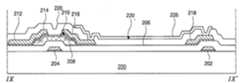
도 10a 내지 도 10e는 도 9의 Ⅸ-Ⅸ`를 따라 절단하여, 본 발명의 공정 순서에 따라 도시한 공정 단면도이다.
10A to 10E are sectional views taken along the line VII-VII of FIG. 9 and shown in the process sequence of the present invention.
〈도면의 주요부분에 대한 부호의 설명〉<Explanation of symbols for main parts of drawing>
200 : 기판(유리기판) 202 : 게이트 배선200: substrate (glass substrate) 202: gate wiring
204 : 게이트 전극 206 : 게이트 절연막204: gate electrode 206: gate insulating film
208 : 액티브층 210 : 오믹 콘택층208
212 : 데이터 배선 214 : 소스 전극212: data wiring 214: source electrode
216 : 드레인 전극 218 : 섬형상의 금속층216: drain electrode 218: island-like metal layer
220 : 보호막 222 : 화소 전극
220: protective film 222: pixel electrode
본 발명은 액정표시장치에 관한 것으로 특히, 액정표시장치용 어레이기판에 구성되는 금속배선의 형성방법에 관한 것이다.BACKGROUND OF THE INVENTION 1. Field of the Invention The present invention relates to a liquid crystal display device, and more particularly, to a method for forming a metal wiring formed in an array substrate for a liquid crystal display device.
이하, 도면을 참조하여 일반적인 액정표시장치의 구성과 그 동작특성에 대해 설명한다.Hereinafter, a configuration and operation characteristics of a general liquid crystal display device will be described with reference to the drawings.
도 1은 액정표시장치를 개략적으로 도시한 도면이다.1 is a view schematically showing a liquid crystal display device.
도시한 바와 같이, 액정표시장치(11)는 다수의 서브 컬러필터(7)와 상기 각 컬러필터(7)사이에 구성된 블랙매트릭스(6)와 상기 컬러필터와 블랙매트릭스 상부에 증착된 공통전극(18)이 형성된 상부기판(5)과, 화소영역(P)과 화소영역 상에 형성된 화소전극(17)과 스위칭소자(T)와 어레이배선이 형성된 하부기판(10)으로 구성되며, 상기 상부기판(5)과 하부기판(10) 사이에는 액정(9)이 충진되어 있다.As shown in the drawing, the liquid
상기 하부기판(10)은 어레이기판(array substrate)이라고도 하며, 스위칭 소 자인 박막트랜지스터(T)가 매트릭스형태(matrix type)로 위치하고, 이러한 다수의 박막트랜지스터(TFT)를 교차하여 지나가는 게이트배선(14)과 데이터배선(22)이 형성된다.The
이때, 상기 화소영역(P)은 상기 게이트배선(14)과 데이터배선(22)이 교차하여 정의되는 영역이며, 상기 화소영역(P)상에는 투명한 화소전극(17)이 형성된다.In this case, the pixel area P is an area defined by the
상기 화소전극(17)과 공통전극(18)은 인듐-틴-옥사이드(indium-tin-oxide : ITO) 같이 빛의 투과율이 비교적 뛰어난 투명 도전성금속을 사용한다.The
도시하지는 않았지만 상기 액정패널(11)의 하부에는 백라이트를 구성하며, 상기 백라이트는 전원이 인가되면 언제나 켜져 있는 상태이다.Although not shown, a backlight is formed under the
상기 게이트 배선(14)을 통해 박막트랜지스터(T)의 게이트 전극에 주사신호가 인가되면, 상기 박막트랜지스터(T)의 채널이 열리게 되고, 상기 데이터 배선(22)에서 박막트랜지스터(T)를 거쳐 상기 화소전극(17)으로 입력된다.When a scan signal is applied to the gate electrode of the thin film transistor T through the
상기 화소전극에 입력된 신호에 따라 화소전극과 상기 공통전극의 사이에 전계가 분포하게 되며, 전계의 세기에 따라 상기 액정(9)의 배열방향이 달라진다.The electric field is distributed between the pixel electrode and the common electrode according to the signal input to the pixel electrode, and the arrangement direction of the
이때, 상기 액정(9)의 배열 방향에 따라 상기 백라이트(미도시)에서 조사된 빛의 출사량이 달라지게 되며, 이로 인해 관찰자는 상기 데이터 신호를 화상으로 관찰하게 된다.In this case, the emission amount of light irradiated from the backlight (not shown) varies according to the arrangement direction of the
이때, 액정패널(11)의 화질을 결정하는 요소들은 매우 다양하며, 그 가운데 상기 어레이기판에 구성된 게이트 배선(14)과 데이터 배선(22)의 저항은 액정패널의 화질을 결정화는 매우 중요한 요소이다.At this time, the factors for determining the image quality of the
즉, 상기 게이트 배선(14)과 데이터 배선(22)의 저항이 작으면 신호지연을 줄일 수 있고 그에 따라 화질이 개선되는 결과를 얻을 수 있다.In other words, if the resistances of the
이를 위해, 종래에는 게이트 배선(14) 또는 데이터 배선(22)으로 저저항 물질인 구리를 사용하였는데, 상기 구리를 게이트 배선(14)으로 사용할 경우에는 구리가 기판과의 접촉특성이 좋지 않아 이를 해결하기 위해, 기판과 구리층 사이에 버퍼층(buffer layer)으로서 티타늄(Ti) 또는 몰리브덴(Mo)을 사용하였다.To this end, conventionally, a low-resistance material copper was used as the
이하, 도 2를 참조하여, 상기 어레이기판의 한 화소에 대한 단면구조를 알아 본다.Hereinafter, a cross-sectional structure of one pixel of the array substrate will be described with reference to FIG. 2.
도 2는 도 1의 Ⅱ-Ⅱ`를 따라 절단한 단면도이다.FIG. 2 is a cross-sectional view taken along line II-II ′ of FIG. 1.
도시한 바와 같이, 기판(10)상에는 다수의 서로 수직하게 교차하여 화소영역(P)을 정의하는 게이트 배선(14)과 데이터 배선(22)이 구성되고, 상기 두 배선(14,22)의 교차지점에는 게이트 전극(30)과 액티브층(34)과 소스 전극(38)과 드레인 전극(40)을 포함하는 박막트랜지스터(T)와, 화소영역(P)에는 상기 드레인 전극(40)과 접촉하는 투명한 화소전극(17)이 구성된다.As shown, a plurality of
일반적으로, 상기 게이트 배선(14)은 동일층 동일물질로 형성되고, 상기 데이터 배선(22)은 상기 소스 및 드레인 전극(38,40)과 동일층 동일물질로 형성된다.In general, the
이때, 액티브층(34)과 소스 및 드레인 전극(38,40)과 게이트 전극(30)사이에는 게이트 절연막(32)이 위치한다.In this case, the
전술한 구성에서, 상기 게이트 전극(30)과 소스 및 드레인 전극(38,40)을 구리/티타늄(Cu/Ti) 또는 구리/몰리브덴(Cu/Mo)의 복층으로 구성할 수 있다.In the above configuration, the
이때, 상기 복층의 금속 중 구리막의 식각을 위하여 옥손(2KHSO5 · KHSO4,· K2SO4)과 구리/티타늄(Cu/Ti)이중 막의 경우 티타늄의 식각을 위해 상기 옥손과 불산(HF)과 불화암모늄(NH4F)혼합한 혼합액을 사용하였다.In this case, in the case of a double layer of oxone (2KHSO5 · KHSO4 , · K2 SO4 ) and copper / titanium (Cu / Ti) for etching a copper layer of the metal of the multilayer, the oxone and hydrofluoric acid (HF) for etching titanium A mixed solution of ammonium fluoride (NH4 F) was used.
상기 구리/티타늄(Cu/Ti)구조의 배선을 전술한 식각용액을 이용하여 습식식각을 진행하였을 경우에는, 상기 식각용액 성분에 F-이온이 포함되어 있기 때문에, 상기 복층의 금속을 게이트 배선(14)에 적용할 경우에는 하부의 유리기판(10)의 표면이 식각되는 문제가 발생하고 이러한 불균일한 식각은 액정패널에서의 얼룩불량을 유발한다.When the wet etching of the copper / titanium (Cu / Ti) structure is performed using the above-described etching solution, since the F− ion is included in the etching solution component, the multilayer metal may be gate-wired ( 14), the surface of the
또한, 상기 복층의 금속을 데이터 배선(22)에 적용할 경우에는 하부의 게이트 절연막(32)이 필연적으로 식각되며 이러한 게이트 절연막(32)의 불균일한 식각상태 또한 액정패널에서의 얼룩불량을 유발한다.In addition, when the metal of the multilayer is applied to the
이하, 도 3과 도 4는 유리기판에 상기 복층(구리/티타늄)의 금속을 증착하고 패턴한 결과를 주사전자현미경으로 찍은 사진이다.3 and 4 are photographs taken with a scanning electron microscope showing the result of depositing and patterning the metal of the multilayer (copper / titanium) on a glass substrate.
도 3에 보이는 바와 같이, 상기 복층의 금속을 패터닝한 결과를 보면, 식각 용액에 의해 노출된 기판(50)의 표면이 매우 거칠어진 것을 관찰할 수 있다.As shown in FIG. 3, when the metal of the multilayer is patterned, the surface of the
상기 기판(50)의 깍인 상태를 더욱 자세히 확대한 사진이 도 4이며 보이는 바와 같이, 기판(50)상에 티타늄층(52a)과 구리층(52b)이 증착되어 있고, 상기 티타늄(Ti)층(52a) 하부로 유리 기판(50)이 침식되어 있는 것을 관찰할 수 있다.As shown in FIG. 4, an enlarged detail of the cutting state of the
자세히는, 상기 유리기판(50)은 표면으로부터 약 400Å정도 깍이는 것으로 측정 되었다.In detail, the
반면, 구리/몰리(Cu/Mo)의 이중층일 경우에, 구리/몰리(Cu/Mo)을 패턴하는 식각용액은 유리기판에 영향은 주지 않으나, 몰리브덴 금속 자체가 데미지를 입게 되어 오히려 구리층을 들뜨게 하는 불량을 유발한다.On the other hand, in the case of a double layer of copper / mol (Cu / Mo), the etching solution patterning the copper / mol (Cu / Mo) does not affect the glass substrate, but the molybdenum metal itself is damaged and thus the copper layer is damaged. Cause excitement failure.
이하, 도 5와 도 6을 참조하여 설명한다. 도 5와 도 6은 유리기판에 상기 복층의 금속(Cu/Mo)을 증착하고 패턴한 결과를 주사전자현미경으로 찍은 사진이다.A description with reference to FIGS. 5 and 6 is as follows. 5 and 6 are photographs taken by scanning electron microscopy to deposit and pattern the multilayer metal (Cu / Mo) on a glass substrate.
도 5에 보이는 바와 같이, 유리기판(50)상에 증착된 구리/몰리브덴(Cu/Mo)층(60)을 패턴한 결과, 하부의 유기리판(50)의 표면은 데미지를 입지 않아 매우 평탄한 상태임을 관찰할 수 있다.As shown in FIG. 5, as a result of patterning the copper / molybdenum (Cu / Mo)
반면, 도 6에 보이는 바와 같이, 몰리브덴(Mo)층(60a)과 기판(50) 사이에 위치하는 구리층(60b)이 안쪽으로 깍여져 있는 상태(A)인 것을 관찰할 수 있다.On the other hand, as shown in FIG. 6, it can be observed that the
상기 도 3 내지 도 6에 의해, 상기 구리층(60b)의 하부에 버퍼층으로 사용되는 금속이 티타늄(Ti)일 경우에는, 상기 구리/티타늄(Cu/Ti)을 식각하는 식각용액에 의해 유리기판의 표면이 심한 데미지를 입게 되고, 상기 구리/몰리브덴(Cu/Mo)일 경우에는 몰리층(60a) 자체가 심하게 깍여 오히려 구리층(60b)을 기판(50)으로부터 들뜨게 만드는 문제가 있는 것을 알 수 있었다.3 to 6, when the metal used as the buffer layer under the
본 발명은 전술한 바와 같은 문제를 해결하기 위한 목적으로 안출된 것으로,The present invention is made for the purpose of solving the above problems,
본 발명에 따른 액정표시장치용 어레이기판은 상기 게이트 배선과 데이터 배 선을 구리/몰리합금(Cu/Mo-alloy)의 복층으로 형성한다.In the array substrate for a liquid crystal display according to the present invention, the gate wiring and the data wiring are formed of a multilayer of copper / mol alloy (Cu / Mo-alloy).
이와 같이 하면, 상기 몰리브합금이 내화학적으로 강하기 때문에 식각액에 의해 과도하게 깍이는 문제가 발생하지 않으며, 물론 유리기판의 손상도 발생하지 않는다.In this case, since the molybdenum alloy is chemically strong, there is no problem of excessive chipping by the etching solution, and of course, no damage to the glass substrate occurs.
따라서, 동작특성이 개선되고 화질불량이 발생하지 않는 고품질의 액정표시장치를 제작 할 수 있다.
Therefore, it is possible to manufacture a high quality liquid crystal display device in which the operation characteristics are improved and the image quality defect does not occur.
전술한 목적을 달성하기 위한 본 발명에 따른 액정표시장치용 어레이기판은 기판 상에 몰리합금(Mo-alloy)층과 구리(Cu)가 순차적으로 증착되어 패턴된 게이트 전극과, 게이트 배선과; 상기 게이트 전극 상부의 게이트 절연막 상에 위치한 액티브층과 오믹 콘택층과; 상기 오믹 콘택층의 일측에 걸쳐 구성되며, 소스 전극과 이와는 소정간격 이격된 드레인 전극과, 소스 전극과 연결되며 상기 게이트 배선과 수직하게 교차하여 화소영역을 정의하는 데이터 배선과; 상기 게이트 절연막 상에 형성되며 상기 게이트배선과 중첩하는 섬형상의 금속패턴과; 상기 소스 및 드레인 전극과 상기 데이터 배선 그리고 상기 금속패턴의 상부에 구성되고, 상기 드레인 전극과 상기 금속패턴의 일부를 노출하는 보호막과; 상기 노출된 드레인 전극 및 상기 금속패턴과 접촉하면서 상기 화소영역에 위치하는 투명한 화소전극을 포함하며, 상기 소스 및 드레인전극은 구리(Cu) 또는 구리/몰리합금(Cu/Mo-alloy)층으로 구성되는 것을 특징으로 하는 액정표시장치용 어레이기판을 제공한다.
상기 데이터 배선은 구리(Cu) 또는 구리/몰리합금(Cu/Mo-alloy)층으로 구성된다.
또한, 본 발명은 기판 상에 몰리합금(Mo-alloy)층과 구리(Cu)를 순차적으로 증착하고 패턴하여, 일 방향으로 연장된 게이트 배선과 이에 연결된 게이트 전극을 형성하는 단계와; 상기 게이트 배선과 상기 게이트 전극이 형성된 상기 기판의 전면에 게이트 절연막을 형성하는 단계와; 상기 게이트 전극 상부의 상기 게이트 절연막 상에 액티브층과 오믹 콘택층을 적층하는 단계와; 상기 오믹 콘택층 상에 소정간격 이격된 소스 전극과 드레인 전극과, 상기 게이트 배선과 수직하게 교차하여 화소영역을 정의하는 데이터 배선을 형성하는 단계와; 상기 게이트 절연막 상에 형성되며 상기 게이트배선과 중첩하는 섬형상의 금속패턴을 형성하는 단계와; 상기 소스 및 드레인 전극이 형성된 상기 기판의 전면에 상기 드레인 전극과 상기 금속패턴의 일부를 노출하는 보호막을 형성하는 단계와; 상기 노출된 드레인 전극 및 상기 금속패턴과 접촉하면서 상기 화소영역에 위치하는 화소전극을 형성하는 단계를 포함하며, 상기 액티브층, 상기 오믹 콘택층, 상기 소스 및 드레인전극은 일괄 식각되는 것을 특징으로 하는 액정표시장치용 어레이기판 제조방법을 제공한다.
상기 보호막은 질화 실리콘(SiNX)과 산화 실리콘(SiO2)을 포함하는 무기절연물질 그룹과 벤조사이클로부텐(BCB)과 아크릴(acryl)계 수지(resin)를 포함하는 유기절연물질 그룹 중 선택된 하나로 형성되며, 상기 데이터 배선과 소스 및 드레인 전극은 구리 또는 구리/몰리합금(Cu/Mo-alloy)층으로 형성된다.
또한, 상기 몰리합금은 몰리브덴과 텅스텐(W), 네오디뮴(Nd), 니오브(Nb)를 포함하는 합금가능한 금속그룹 중 선택된 하나로 합금되며, 상기 화소전극은 인듐-틴-옥사이드(ITO)와 인듐-징크-옥사이드(IZO)를 포함하는 투명한 도전성 금속그룹 중 선택된 하나로 형성한다.According to an aspect of the present invention, there is provided an array substrate for a liquid crystal display device comprising: a gate electrode patterned by sequentially depositing a mol-alloy layer and copper (Cu) on a substrate, and a gate wiring; An active layer and an ohmic contact layer on the gate insulating layer on the gate electrode; A data line formed over one side of the ohmic contact layer and connected to a source electrode, a drain electrode spaced apart from the predetermined distance, and a data line connected to the source electrode and vertically crossing the gate line to define a pixel region; An island-shaped metal pattern formed on the gate insulating film and overlapping the gate wiring; A passivation layer formed on the source and drain electrodes, the data line, and the metal pattern and exposing a part of the drain electrode and the metal pattern; And a transparent pixel electrode positioned in the pixel region while in contact with the exposed drain electrode and the metal pattern, wherein the source and drain electrodes are formed of a copper (Cu) or a copper / mol alloy layer. An array substrate for a liquid crystal display device is provided.
The data line is composed of a copper (Cu) or a copper / mol alloy layer.
In addition, the present invention comprises the steps of sequentially depositing and patterning a Mo-alloy (Mo-alloy) layer and copper (Cu) on the substrate, to form a gate wiring extending in one direction and a gate electrode connected thereto; Forming a gate insulating film on an entire surface of the substrate on which the gate wiring and the gate electrode are formed; Stacking an active layer and an ohmic contact layer on the gate insulating layer on the gate electrode; Forming a source electrode and a drain electrode spaced apart from each other by a predetermined distance on the ohmic contact layer, and a data line defining a pixel area by crossing the gate line perpendicularly; Forming an island-shaped metal pattern formed on the gate insulating layer and overlapping the gate wiring; Forming a passivation layer exposing a portion of the drain electrode and the metal pattern on an entire surface of the substrate on which the source and drain electrodes are formed; And forming a pixel electrode positioned in the pixel region while contacting the exposed drain electrode and the metal pattern, wherein the active layer, the ohmic contact layer, the source and the drain electrode are collectively etched. A method of manufacturing an array substrate for a liquid crystal display device is provided.
The passivation layer is selected from an inorganic insulating material group including silicon nitride (SiNX ) and silicon oxide (SiO2 ), and an organic insulating material group including benzocyclobutene (BCB) and an acrylic resin (resin). The data line and the source and drain electrodes are formed of a copper or copper / mol-alloy (Cu / Mo-alloy) layer.
In addition, the molybdenum alloy is alloyed with one selected from the group of alloyable metals including molybdenum and tungsten (W), neodymium (Nd) and niobium (Nb), and the pixel electrode is made of indium tin oxide (ITO) and indium- It is formed of a selected one of the transparent conductive metal group containing zinc oxide (IZO).
삭제delete
삭제delete
삭제delete
삭제delete
삭제delete
삭제delete
-- 실시예 --Example
본 발명의 특징은 액정표시장치용 어레이기판을 구성하는 게이트 배선과 데이터 배선을 형성할 때, 구리/몰리합금(Cu/Mo-alloy)의 이중층으로 형성하는 것을 특징으로 한다.The present invention is characterized in that when the gate wiring and the data wiring forming the array substrate for the liquid crystal display device are formed, a double layer of Cu / Mo-alloy is formed.
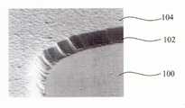
도 7과 도 8은 유리기판 상에 몰리합금(Mo-alloy)과 구리(Cu)를 순차적으로 증착한 시편을 주사전자 현미경(SEM)을 통해 찍은 평면을 나타낸 사진과, 단면을 나타낸 사진이다.7 and 8 are photographs showing a plane taken through a scanning electron microscope (SEM) and a cross section of a specimen in which molybdenum (Mo-alloy) and copper (Cu) are sequentially deposited on a glass substrate.
도 7에 보이는 바와 같이, 유리 기판(100)상에 몰리브합금층(102)과 구리층(104)을 순차적으로 증착하고 패턴한 결과, 노출된 유리기판(100)의 표면이 매끄러운 상태임을 알 수 있다.As shown in FIG. 7, the
이때, 상기 몰리합금층(102)은 대략 10Å~500Å의 두께로 증착하고, 상기 구리층(104)은 500Å~5000Å의 두께로 증착한다.In this case, the
더욱 자세히는 도 8에 보이는 바와 같이, 유리기판(100)상에 몰리브덴 합금층(102)과 구리층(104)이 순차적으로 적층된 것이 보이고, 상기 구리층(104)과 기판(100)사이에 구성된 몰리합금층(102)은 구리층(104)의 하부로 침식되지 않았음을 알 수 있다. 즉, 금속층(102,104)의 측면(B)이 테이퍼지게 식각됨을 알 수 있다.More specifically, as shown in FIG. 8, the
결과적으로, 상기 구리층(104)의 하부에 버퍼층으로서 몰리합금층(102)을 선증착하게 되면, 식각액에 의해 유리기판(100)의 표면과 패턴된 금속 자체가 손상되는 불량이 발생하지 않는다.As a result, when the
이때, 상기 몰리브덴과 합금되는 물질로는텅스텐(W), 네오디뮴(Nd), 니오브(Nb)등이 있다.In this case, as the material alloyed with molybdenum Tungsten (W), neodymium (Nd), niobium (Nb) and the like.
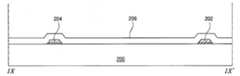
이하, 도 9는 액정표시장치용 어레이기판의 일부를 확대한 확대 평면도이다.9 is an enlarged plan view of an enlarged portion of an array substrate for a liquid crystal display device.
도시한 바와 같이, 기판(200)상에 서로 수직하게 교차하여 화소영역(서브픽셀영역)을 정의하는 게이트 배선(202)과 데이터배선(212)을 형성한다.As shown in the drawing, a
상기 두 배선(202,212)의 교차지점에는 게이트 전극(204)과 액티브층(208)과 소스 전극(214)과 드레인 전극(216)을 포함하는 박막트랜지스터(T)를 형성한다.A thin film transistor T including a
상기 화소영역(P)에는 상기 드레인 전극(216)과 접촉하는 투명한 화소전극(226)이 구성되며, 상기 화소영역(P)을 정의하는 게이트 배선(202)의 일부 상부에는 스토리지 캐패시터(C)를 구성한다.The pixel region P includes a
이때, 상기 스토리지 캐패시터(C)의 제 1 스토리지 전극은 상기 게이트 배선(202)의 일부이며, 제 2 스토리지 전극은 상기 화소전극(226)과 접촉하는 섬형상의 금속층(218)이다.In this case, the first storage electrode of the storage capacitor C is part of the
전술한 구성에서, 상기 게이트 배선(202)과 데이터 배선(212)은 구리/몰리합금(Cu/Mo-ally)층으로 형성된 것을 특징으로 한다. 이때, 상기 데이터 배선(212)은 구리(Cu) 만으로 형성할 수도 있다.In the above-described configuration, the
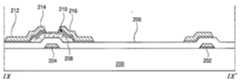
이하, 도 10a 내지 도 10e를 참조하여, 전술한 바와 같은 금속층으로 제작된 배선을 포함하는 액정표시장치용 어레이기판의 제조공정을 공정 순서대로 설명한다. (도 9의 Ⅸ-Ⅸ`를 따라 절단한 단면도이다.)Hereinafter, referring to FIGS. 10A to 10E, a manufacturing process of an array substrate for a liquid crystal display device including a wiring made of the metal layer as described above will be described in a process order. (It is sectional drawing cut along the line VII-VII of FIG. 9).
도 10a에 도시한 바와 같이, 절연기판(유기기판)(200)상에 몰리합금(Mo-alloy)과 구리를 순차적으로 적층하고 패턴하여, 게이트 배선(202)과 이에 연결된 게이트 전극(204)을 형성한다.As shown in FIG. 10A, a molten alloy and copper are sequentially stacked and patterned on an insulating substrate (organic substrate) 200 to form a
이때, 상기 몰리합금(Mo-alloy)층은 대략 10Å~500Å의 두께로 증착하고, 상기 구리는 대략 500Å~5000Å의 두께로 증착하여 형성한다.At this time, the molybdenum (Mo-alloy) layer is deposited to a thickness of about 10 ~ 500Å, and the copper is formed by depositing to a thickness of about 500 ~ 5000Å.
다음으로, 상기 게이트 배선(202)과 게이트 전극(204)이 형성된 기판(200)의 전면에 산화 실리콘(SiO2)과 질화 실리콘(SiNX)을 포함하는 무기절연물질 그룹 중 선택된 하나를 증착하여 게이트 절연막(206)을 형성한다.Next, one selected from the group of inorganic insulating materials including silicon oxide (SiO2 ) and silicon nitride (SiNX ) is deposited on the entire surface of the
도 10b에 도시한 바와 같이, 상기 게이트 절연막(206)이 형성된 기판(200)의 전면에 비정질 실리콘(a-Si:H)을 증착하고, 상기 비정질 실리콘의 표면에 불순물 이온(n+ 또는 p+)을 도핑하거나, 별도의 불순물 비정질 실리콘(n+ 또는 p+a-Si:H)을 증착하고 패턴하여, 상기 게이트 전극(204)상부의 게이트 절연막(206) 상에 액티브층(208)과 오믹 콘택층(210)을 형성한다.As shown in FIG. 10B, amorphous silicon (a-Si: H) is deposited on the entire surface of the
다음으로, 도 10c에 도시한 바와 같이, 상기 액티브층(208)과 오믹 콘택층(210)이 형성된 기판(200)의 전면에 앞서 설명한 몰리합금(Mo-alloy)물질과 구리(Cu)를 순차적으로 증착하고 패턴하여, 상기 게이트 배선(202)과는 수직하게 교차하여 화소영역(P)을 정의하는 데이터 배선(212)과, 상기 데이터 배선(212)에서 상기 게이트 전극(204)의 일측 상부로 연장된 소스 전극(214)과 이와는 소정간격 이격된 드레인 전극(216)을 형성한다.Next, as illustrated in FIG. 10C, the mol-alloy material and copper (Cu) described above are sequentially formed on the entire surface of the
동시에, 상기 화소영역(P)을 정의하는 게이트 배선(202)의 일부 상부에 섬형상의 금속층(218)을 형성한다.At the same time, an island-shaped
이때, 상기 데이터 배선(212)은 구리/몰리합금(Cu/Mo-alloy)뿐 아니라, 구리 만을 증착하여 형성할 수 도 있다.In this case, the
상기 몰리합금(Mo-alloy)은 상기 액티브층(208)과의 접촉특성이 양호한 특성을 가지며, 실리콘 이온이 구리로 확산하는 것을 방지하는 목적으로 사용된다.The Mo-alloy has a good contact property with the
다음으로, 도 10d에 도시한 바와 같이, 상기 데이터 배선(212)과 소스 및 드레인 전극(214,216)이 형성된 기판(200)의 전면에 질화 실리콘(SiNx)과 산화 실리콘(SiO2)을 포함하는 무기절연물질 또는 벤조사이클로부텐(BCB)과 아크릴(acryl)계수지(resin)를 포함하는 유기절연물질그룹 중 선택된 하나를 증착 또는 도포하여 보호막(220)을 형성한다.Next, as shown in FIG. 10D, silicon nitride (SiNx ) and silicon oxide (SiO2 ) are formed on the entire surface of the
다음으로, 상기 보호막(220)을 패턴하여 상기 드레인 전극(216)과 상기 섬형상 금속층(218)의 일부를 노출하는 드레인 콘택홀(222)과 스토리지 콘택홀(224)을 형성한다.Next, the
도 10e에 도시한 바와 같이, 상기 보호막(220)의 상부에 인듐-틴-옥사이드(ITO)와 인듐-징크-옥사이드(IZO)를 포함하는 투명한 도전성 금속그룹 중 선택된 하나를 증착하고 패턴하여, 상기 노출된 드레인 전극(216)과 섬형상의 금속층(218)과 접촉하면서 화소영역(P)에 위치하는 화소전극(226)을 형성한다.As shown in FIG. 10E, a selected one of a transparent conductive metal group including indium tin oxide (ITO) and indium zinc oxide (IZO) is deposited and patterned on the
전술한 바와 같은 공정을 통해 본 발명에 따른 액정표시장치용 어레이기판을 제작할 수 있다.
Through the process as described above it can be produced an array substrate for a liquid crystal display device according to the present invention.
본 발명에 따른 구리/몰리 합금 이중층으로 게이트 배선과 데이터 배선을 형성하게 되면, 유리기판의 표면이나 게이트 배선 상부의 게이트 절연막에 데미지가 발생하지 않아 제품의 수율을 개선하는 장점이 있다.When the gate wiring and the data wiring are formed of the copper / molley alloy double layer according to the present invention, damage does not occur on the surface of the glass substrate or the gate insulating film on the gate wiring, thereby improving the yield of the product.
또한, 전술한 이중구성으로 인해, 배선을 저항이 낮은 구리배선으로 형성하는 것이 가능해지기 때문에 고화질의 액정표시장치를 제작할 수 있는 효과가 있다.In addition, the above-described dual configuration makes it possible to form the wiring with a copper wiring having a low resistance, so that there is an effect that a high-quality liquid crystal display device can be manufactured.
Claims (7)
Translated fromKoreanPriority Applications (5)
| Application Number | Priority Date | Filing Date | Title |
|---|---|---|---|
| KR1020020069285AKR100883769B1 (en) | 2002-11-08 | 2002-11-08 | Manufacturing method of array substrate for liquid crystal display device |
| JP2003301679AJP2004163901A (en) | 2002-11-08 | 2003-08-26 | Array substrate for liquid crystal display device and method of manufacturing the same |
| US10/685,419US7061565B2 (en) | 2002-11-08 | 2003-10-16 | Array substrate having double-layered metal patterns and method of fabricating the same |
| US11/410,815US20060192907A1 (en) | 2002-11-08 | 2006-04-26 | Method of fabricating array substrate having double-layered patterns |
| US12/320,133US8514340B2 (en) | 2002-11-08 | 2009-01-16 | Method of fabricating array substrate having double-layered patterns |
Applications Claiming Priority (1)
| Application Number | Priority Date | Filing Date | Title |
|---|---|---|---|
| KR1020020069285AKR100883769B1 (en) | 2002-11-08 | 2002-11-08 | Manufacturing method of array substrate for liquid crystal display device |
Publications (2)
| Publication Number | Publication Date |
|---|---|
| KR20040040929A KR20040040929A (en) | 2004-05-13 |
| KR100883769B1true KR100883769B1 (en) | 2009-02-18 |
Family
ID=36931645
Family Applications (1)
| Application Number | Title | Priority Date | Filing Date |
|---|---|---|---|
| KR1020020069285AExpired - LifetimeKR100883769B1 (en) | 2002-11-08 | 2002-11-08 | Manufacturing method of array substrate for liquid crystal display device |
Country Status (3)
| Country | Link |
|---|---|
| US (2) | US7061565B2 (en) |
| JP (1) | JP2004163901A (en) |
| KR (1) | KR100883769B1 (en) |
Cited By (1)
| Publication number | Priority date | Publication date | Assignee | Title |
|---|---|---|---|---|
| KR20230034264A (en)* | 2011-10-19 | 2023-03-09 | 가부시키가이샤 한도오따이 에네루기 켄큐쇼 | Semiconductor device and manufacturing method thereof |
Families Citing this family (58)
| Publication number | Priority date | Publication date | Assignee | Title |
|---|---|---|---|---|
| US7626665B2 (en) | 2004-08-31 | 2009-12-01 | Tohoku University | Copper alloys and liquid-crystal display device |
| US8514340B2 (en) | 2002-11-08 | 2013-08-20 | Lg Display Co., Ltd. | Method of fabricating array substrate having double-layered patterns |
| US7940361B2 (en) | 2004-08-31 | 2011-05-10 | Advanced Interconnect Materials, Llc | Copper alloy and liquid-crystal display device |
| KR101061850B1 (en) | 2004-09-08 | 2011-09-02 | 삼성전자주식회사 | Thin film transistor array panel and manufacturing method thereof |
| KR101058458B1 (en) | 2004-09-22 | 2011-08-24 | 엘지디스플레이 주식회사 | Array substrate for liquid crystal display device using low molecular organic semiconductor material and manufacturing method thereof |
| KR101046928B1 (en)* | 2004-09-24 | 2011-07-06 | 삼성전자주식회사 | Thin film transistor array panel and manufacturing method |
| KR101122228B1 (en) | 2004-10-26 | 2012-03-19 | 삼성전자주식회사 | Thin film transistor array panel and method for manufacturing the same |
| KR20060062913A (en) | 2004-12-06 | 2006-06-12 | 삼성전자주식회사 | Display device wiring and thin film transistor display panel including the wiring and manufacturing method thereof |
| KR101160829B1 (en) | 2005-02-15 | 2012-06-29 | 삼성전자주식회사 | Etchant composition and method for thin film transistor array panel |
| KR101191402B1 (en) | 2005-07-25 | 2012-10-16 | 삼성디스플레이 주식회사 | Stripper composite for photoresist and method for fabricating interconnection line and method for fabricating thin film transistor substrate using the same |
| US7576359B2 (en)* | 2005-08-12 | 2009-08-18 | Semiconductor Energy Laboratory Co., Ltd. | Liquid crystal display device and method for manufacturing the same |
| KR101244895B1 (en)* | 2006-04-06 | 2013-03-18 | 삼성디스플레이 주식회사 | Method for fabricating thin film transistor plate |
| JP4713433B2 (en)* | 2006-05-15 | 2011-06-29 | エルジー ディスプレイ カンパニー リミテッド | Thin film transistor |
| KR101284697B1 (en)* | 2006-06-30 | 2013-07-23 | 엘지디스플레이 주식회사 | An array substrate for LCD and method for fabricating thereof |
| KR100748110B1 (en)* | 2006-09-11 | 2007-08-09 | (주)비스마스 | Multi-directional lighting system for glass substrate inspection |
| KR101326128B1 (en)* | 2006-09-29 | 2013-11-06 | 삼성디스플레이 주식회사 | Wire for display device, etchant, thin film transistor array panel and method for manufacturing the same |
| TW200822232A (en)* | 2006-11-06 | 2008-05-16 | Chunghwa Picture Tubes Ltd | Thin film transistor and fabrication method thereof |
| JP5280671B2 (en)* | 2006-12-20 | 2013-09-04 | 富士フイルム株式会社 | Image detector and radiation detection system |
| EP1936694B1 (en)* | 2006-12-20 | 2014-11-26 | FUJIFILM Corporation | Image detector and radiation detecting system |
| US7642552B2 (en) | 2007-01-12 | 2010-01-05 | Tohoku University | Liquid crystal display device and manufacturing method therefor |
| US7633164B2 (en) | 2007-04-10 | 2009-12-15 | Tohoku University | Liquid crystal display device and manufacturing method therefor |
| US7782413B2 (en) | 2007-05-09 | 2010-08-24 | Tohoku University | Liquid crystal display device and manufacturing method therefor |
| WO2008153087A1 (en)* | 2007-06-15 | 2008-12-18 | Semiconductor Energy Laboratory Co., Ltd. | Display device |
| JP5571887B2 (en) | 2008-08-19 | 2014-08-13 | アルティアム サービシズ リミテッド エルエルシー | Liquid crystal display device and manufacturing method thereof |
| JP5269533B2 (en) | 2008-09-26 | 2013-08-21 | 三菱マテリアル株式会社 | Thin film transistor |
| JP5360959B2 (en) | 2008-10-24 | 2013-12-04 | 三菱マテリアル株式会社 | Thin film transistor having high adhesion strength between barrier film, drain electrode film and source electrode film |
| US8114720B2 (en) | 2008-12-25 | 2012-02-14 | Semiconductor Energy Laboratory Co., Ltd. | Semiconductor device and manufacturing method thereof |
| US20110227085A1 (en)* | 2008-12-26 | 2011-09-22 | Sharp Kabushiki Kaisha | Substrate for use in display panel, and display panel including same |
| CN101957530B (en)* | 2009-07-17 | 2013-07-24 | 北京京东方光电科技有限公司 | TFT-LCD (Thin Film Transistor-Liquid Crystal Display) array baseplate and manufacturing method thereof |
| CN102484138B (en)* | 2009-08-28 | 2014-03-12 | 株式会社爱发科 | Wiring layer, semiconductor device, liquid crystal display device |
| CN102598278B (en) | 2009-10-09 | 2015-04-08 | 株式会社半导体能源研究所 | Semiconductor device |
| WO2011043194A1 (en) | 2009-10-09 | 2011-04-14 | Semiconductor Energy Laboratory Co., Ltd. | Semiconductor device and method for manufacturing the same |
| CN102576736B (en) | 2009-10-09 | 2015-05-13 | 株式会社半导体能源研究所 | Semiconductor device and method for manufacturing the same |
| KR101604650B1 (en)* | 2009-10-27 | 2016-03-28 | 삼성디스플레이 주식회사 | Display substrate, method for manufacturing the same and method for manufacturing display panel |
| KR101802406B1 (en) | 2009-11-27 | 2017-11-28 | 가부시키가이샤 한도오따이 에네루기 켄큐쇼 | Semiconductor device and method for manufacturing the same |
| JP5403527B2 (en) | 2010-07-02 | 2014-01-29 | 合同会社先端配線材料研究所 | Semiconductor device |
| JP5453663B2 (en) | 2010-07-02 | 2014-03-26 | 合同会社先端配線材料研究所 | Thin film transistor |
| KR101256276B1 (en)* | 2010-08-25 | 2013-04-18 | 플란제 에스이 | Etchant composition for etching a conductive multi-layer film and etching method using the same |
| CN101980368A (en)* | 2010-09-09 | 2011-02-23 | 中国科学院深圳先进技术研究院 | Copper indium gallium selenide thin film battery and its preparation method |
| US8558960B2 (en) | 2010-09-13 | 2013-10-15 | Semiconductor Energy Laboratory Co., Ltd. | Liquid crystal display device and method for manufacturing the same |
| JP5429718B2 (en) | 2011-03-08 | 2014-02-26 | 合同会社先端配線材料研究所 | Oxide semiconductor electrode and method for forming the same |
| JP5977569B2 (en) | 2011-04-22 | 2016-08-24 | 株式会社神戸製鋼所 | THIN FILM TRANSISTOR STRUCTURE, AND THIN FILM TRANSISTOR AND DISPLAY DEVICE HAVING THE STRUCTURE |
| CN102983101B (en)* | 2011-08-04 | 2015-06-17 | 东友精细化工有限公司 | Manufacturing method of array substrate for liquid crystal display |
| KR101913207B1 (en) | 2011-10-12 | 2018-11-01 | 삼성디스플레이 주식회사 | Thin film transistor, thin film transistor panel and method of manufacturing the same |
| JP5888501B2 (en) | 2012-02-16 | 2016-03-22 | 三菱マテリアル株式会社 | Thin film wiring formation method |
| KR20130105392A (en) | 2012-03-14 | 2013-09-25 | 가부시키가이샤 한도오따이 에네루기 켄큐쇼 | Semiconductor device |
| US9166054B2 (en) | 2012-04-13 | 2015-10-20 | Semiconductor Energy Laboratory Co., Ltd. | Semiconductor device and manufacturing method thereof |
| JP2014045175A (en) | 2012-08-02 | 2014-03-13 | Semiconductor Energy Lab Co Ltd | Semiconductor device |
| KR102094841B1 (en) | 2013-05-16 | 2020-03-31 | 삼성디스플레이 주식회사 | Display apparatus and method of manufacturing the same |
| CN103441119B (en)* | 2013-07-05 | 2016-03-30 | 京东方科技集团股份有限公司 | A kind of method, ESD device and display floater manufacturing ESD device |
| KR102255577B1 (en)* | 2014-08-25 | 2021-05-25 | 엘지디스플레이 주식회사 | Etching composition |
| JP2017139433A (en)* | 2016-02-05 | 2017-08-10 | 大日本印刷株式会社 | Through electrode substrate and method for manufacturing the same |
| US10692452B2 (en) | 2017-01-16 | 2020-06-23 | Semiconductor Energy Laboratory Co., Ltd. | Display device |
| WO2020012276A1 (en) | 2018-07-09 | 2020-01-16 | 株式会社半導体エネルギー研究所 | Semiconductor device |
| CN112805838B (en) | 2018-10-10 | 2024-09-20 | 株式会社半导体能源研究所 | Semiconductor devices |
| WO2020089733A1 (en) | 2018-11-02 | 2020-05-07 | 株式会社半導体エネルギー研究所 | Semiconductor device |
| US20220320340A1 (en) | 2019-08-09 | 2022-10-06 | Semiconductor Energy Laboratory Co., Ltd. | Semiconductor device and method for manufacturing semiconductor device |
| TW202414057A (en) | 2020-03-20 | 2024-04-01 | 日商半導體能源研究所股份有限公司 | Semiconductor device and method for manufacturing semiconductor device |
Citations (4)
| Publication number | Priority date | Publication date | Assignee | Title |
|---|---|---|---|---|
| JPH10253976A (en)* | 1997-03-12 | 1998-09-25 | Toshiba Corp | Liquid crystal display device |
| JP2001059191A (en)* | 1999-06-18 | 2001-03-06 | Furontekku:Kk | Etching agent, method of manufacturing electronic device substrate using the same, and electronic device |
| KR20010057663A (en)* | 1999-12-23 | 2001-07-05 | 윤종용 | manufacturing method of a thin film transistor array panel for a liquid crystal display |
| KR20010081966A (en)* | 2000-02-10 | 2001-08-29 | 아끼구사 나오유끼 | Thin film transistor and method for fabricating the same |
Family Cites Families (15)
| Publication number | Priority date | Publication date | Assignee | Title |
|---|---|---|---|---|
| JP2952075B2 (en)* | 1991-06-12 | 1999-09-20 | キヤノン株式会社 | Liquid crystal device manufacturing method |
| KR100247493B1 (en)* | 1996-10-18 | 2000-03-15 | 구본준, 론 위라하디락사 | Structure of active matrix substrate |
| JP4011664B2 (en)* | 1997-02-03 | 2007-11-21 | キヤノン株式会社 | Wiring board manufacturing method |
| US6333518B1 (en)* | 1997-08-26 | 2001-12-25 | Lg Electronics Inc. | Thin-film transistor and method of making same |
| US6323490B1 (en)* | 1998-03-20 | 2001-11-27 | Kabushiki Kaisha Toshiba | X-ray semiconductor detector |
| TW559683B (en)* | 1998-09-21 | 2003-11-01 | Advanced Display Kk | Liquid display device and manufacturing process therefor |
| JP3916334B2 (en)* | 1999-01-13 | 2007-05-16 | シャープ株式会社 | Thin film transistor |
| US6393042B1 (en)* | 1999-03-08 | 2002-05-21 | Semiconductor Energy Laboratory Co., Ltd. | Beam homogenizer and laser irradiation apparatus |
| JP2001013523A (en)* | 1999-06-30 | 2001-01-19 | Nec Corp | Liquid crystal display device and method of manufacturing the same |
| US6686661B1 (en)* | 1999-10-15 | 2004-02-03 | Lg. Philips Lcd Co., Ltd. | Thin film transistor having a copper alloy wire |
| KR100690001B1 (en)* | 2000-02-21 | 2007-03-08 | 엘지.필립스 엘시디 주식회사 | LCD and its manufacturing method |
| JP2001281698A (en)* | 2000-03-30 | 2001-10-10 | Advanced Display Inc | Production method for optoelectronic element |
| KR100379824B1 (en)* | 2000-12-20 | 2003-04-11 | 엘지.필립스 엘시디 주식회사 | Etchant and array substrate for electric device with Cu lines patterend on the array substrate using the etchant |
| KR100412619B1 (en)* | 2001-12-27 | 2003-12-31 | 엘지.필립스 엘시디 주식회사 | Method for Manufacturing of Array Panel for Liquid Crystal Display Device |
| KR100866976B1 (en)* | 2002-09-03 | 2008-11-05 | 엘지디스플레이 주식회사 | Array substrate for LCD and manufacturing method |
- 2002
- 2002-11-08KRKR1020020069285Apatent/KR100883769B1/ennot_activeExpired - Lifetime
- 2003
- 2003-08-26JPJP2003301679Apatent/JP2004163901A/enactivePending
- 2003-10-16USUS10/685,419patent/US7061565B2/ennot_activeExpired - Lifetime
- 2006
- 2006-04-26USUS11/410,815patent/US20060192907A1/ennot_activeAbandoned
Patent Citations (4)
| Publication number | Priority date | Publication date | Assignee | Title |
|---|---|---|---|---|
| JPH10253976A (en)* | 1997-03-12 | 1998-09-25 | Toshiba Corp | Liquid crystal display device |
| JP2001059191A (en)* | 1999-06-18 | 2001-03-06 | Furontekku:Kk | Etching agent, method of manufacturing electronic device substrate using the same, and electronic device |
| KR20010057663A (en)* | 1999-12-23 | 2001-07-05 | 윤종용 | manufacturing method of a thin film transistor array panel for a liquid crystal display |
| KR20010081966A (en)* | 2000-02-10 | 2001-08-29 | 아끼구사 나오유끼 | Thin film transistor and method for fabricating the same |
Cited By (4)
| Publication number | Priority date | Publication date | Assignee | Title |
|---|---|---|---|---|
| KR20230034264A (en)* | 2011-10-19 | 2023-03-09 | 가부시키가이샤 한도오따이 에네루기 켄큐쇼 | Semiconductor device and manufacturing method thereof |
| US11817505B2 (en) | 2011-10-19 | 2023-11-14 | Semiconductor Energy Laboratory Co., Ltd. | Semiconductor device |
| KR102689784B1 (en)* | 2011-10-19 | 2024-07-29 | 가부시키가이샤 한도오따이 에네루기 켄큐쇼 | Semiconductor device and manufacturing method thereof |
| US12376335B2 (en) | 2011-10-19 | 2025-07-29 | Semiconductor Energy Laboratory Co., Ltd. | Semiconductor device and manufacturing method thereof |
Also Published As
| Publication number | Publication date |
|---|---|
| JP2004163901A (en) | 2004-06-10 |
| US7061565B2 (en) | 2006-06-13 |
| KR20040040929A (en) | 2004-05-13 |
| US20060192907A1 (en) | 2006-08-31 |
| US20050018097A1 (en) | 2005-01-27 |
Similar Documents
| Publication | Publication Date | Title |
|---|---|---|
| KR100883769B1 (en) | Manufacturing method of array substrate for liquid crystal display device | |
| KR100726132B1 (en) | Array substrate for liquid crystal display device and manufacturing method | |
| KR100795344B1 (en) | Array substrate for liquid crystal display device and manufacturing method thereof | |
| JP4543385B2 (en) | Manufacturing method of liquid crystal display device | |
| KR100583979B1 (en) | Liquid crystal display device manufacturing method and liquid crystal display device according to the manufacturing method | |
| JP3413000B2 (en) | Active matrix liquid crystal panel | |
| US6731364B2 (en) | Liquid crystal display device | |
| KR101270705B1 (en) | Thin film transistor substrate, method for manufacturing the same and liquid crystal display panel having the same | |
| KR101486180B1 (en) | A method for manufacturing active matrix substrate, display panel, and display device | |
| US6888586B2 (en) | Array substrate for liquid crystal display and method for fabricating the same | |
| TWI247431B (en) | Liquid crystal display unit | |
| KR100673331B1 (en) | Liquid crystal display device manufacturing method and liquid crystal display device according to the manufacturing method | |
| KR100582599B1 (en) | Liquid crystal display device manufacturing method and liquid crystal display device according to the manufacturing method | |
| US8514340B2 (en) | Method of fabricating array substrate having double-layered patterns | |
| KR101046928B1 (en) | Thin film transistor array panel and manufacturing method | |
| KR100904524B1 (en) | Manufacturing method of array substrate for liquid crystal display device | |
| KR100654158B1 (en) | Liquid crystal display device manufacturing method and liquid crystal display device according to the manufacturing method | |
| KR100508000B1 (en) | The substrate for LCD and method for fabricating the same | |
| KR100342860B1 (en) | Liquid crystal display and method for fabricating the same | |
| KR100632216B1 (en) | Array substrate for liquid crystal display device and manufacturing method thereof | |
| KR100660809B1 (en) | Liquid crystal display device manufacturing method and liquid crystal display device according to the manufacturing method | |
| KR100309210B1 (en) | Liquid crystal display and method for fabricating the same | |
| KR20020006376A (en) | A method for fabricating array substrate for liquid crystal display device and the same | |
| KR20020094809A (en) | Fabricating method of thin film transistor - liquid crystal display | |
| KR100905053B1 (en) | Manufacturing method of array substrate for liquid crystal display device including copper wiring |
Legal Events
| Date | Code | Title | Description |
|---|---|---|---|
| PA0109 | Patent application | Patent event code:PA01091R01D Comment text:Patent Application Patent event date:20021108 | |
| PG1501 | Laying open of application | ||
| A201 | Request for examination | ||
| PA0201 | Request for examination | Patent event code:PA02012R01D Patent event date:20071008 Comment text:Request for Examination of Application Patent event code:PA02011R01I Patent event date:20021108 Comment text:Patent Application | |
| E902 | Notification of reason for refusal | ||
| PE0902 | Notice of grounds for rejection | Comment text:Notification of reason for refusal Patent event date:20080529 Patent event code:PE09021S01D | |
| AMND | Amendment | ||
| E601 | Decision to refuse application | ||
| PE0601 | Decision on rejection of patent | Patent event date:20081124 Comment text:Decision to Refuse Application Patent event code:PE06012S01D Patent event date:20080529 Comment text:Notification of reason for refusal Patent event code:PE06011S01I | |
| AMND | Amendment | ||
| J201 | Request for trial against refusal decision | ||
| PJ0201 | Trial against decision of rejection | Patent event date:20081209 Comment text:Request for Trial against Decision on Refusal Patent event code:PJ02012R01D Patent event date:20081124 Comment text:Decision to Refuse Application Patent event code:PJ02011S01I Appeal kind category:Appeal against decision to decline refusal Decision date:20090206 Appeal identifier:2008101013104 Request date:20081209 | |
| PB0901 | Examination by re-examination before a trial | Comment text:Amendment to Specification, etc. Patent event date:20081209 Patent event code:PB09011R02I Comment text:Request for Trial against Decision on Refusal Patent event date:20081209 Patent event code:PB09011R01I Comment text:Amendment to Specification, etc. Patent event date:20080722 Patent event code:PB09011R02I | |
| B701 | Decision to grant | ||
| PB0701 | Decision of registration after re-examination before a trial | Patent event date:20090206 Comment text:Decision to Grant Registration Patent event code:PB07012S01D Patent event date:20090109 Comment text:Transfer of Trial File for Re-examination before a Trial Patent event code:PB07011S01I | |
| GRNT | Written decision to grant | ||
| PR0701 | Registration of establishment | Comment text:Registration of Establishment Patent event date:20090209 Patent event code:PR07011E01D | |
| PR1002 | Payment of registration fee | Payment date:20090210 End annual number:3 Start annual number:1 | |
| PG1601 | Publication of registration | ||
| PR1001 | Payment of annual fee | Payment date:20111221 Start annual number:4 End annual number:4 | |
| FPAY | Annual fee payment | Payment date:20121228 Year of fee payment:5 | |
| PR1001 | Payment of annual fee | Payment date:20121228 Start annual number:5 End annual number:5 | |
| FPAY | Annual fee payment | Payment date:20131227 Year of fee payment:6 | |
| PR1001 | Payment of annual fee | Payment date:20131227 Start annual number:6 End annual number:6 | |
| FPAY | Annual fee payment | Payment date:20150127 Year of fee payment:7 | |
| PR1001 | Payment of annual fee | Payment date:20150127 Start annual number:7 End annual number:7 | |
| FPAY | Annual fee payment | Payment date:20160128 Year of fee payment:8 | |
| PR1001 | Payment of annual fee | Payment date:20160128 Start annual number:8 End annual number:8 | |
| FPAY | Annual fee payment | Payment date:20170116 Year of fee payment:9 | |
| PR1001 | Payment of annual fee | Payment date:20170116 Start annual number:9 End annual number:9 | |
| FPAY | Annual fee payment | Payment date:20190114 Year of fee payment:11 | |
| PR1001 | Payment of annual fee | Payment date:20190114 Start annual number:11 End annual number:11 | |
| PR1001 | Payment of annual fee | Payment date:20210118 Start annual number:13 End annual number:13 | |
| PR1001 | Payment of annual fee | Payment date:20220120 Start annual number:14 End annual number:14 | |
| PC1801 | Expiration of term | Termination date:20230508 Termination category:Expiration of duration |