KR100883026B1 - Image sensor and manufacturing method - Google Patents
Image sensor and manufacturing methodDownload PDFInfo
- Publication number
- KR100883026B1 KR100883026B1KR1020070139371AKR20070139371AKR100883026B1KR 100883026 B1KR100883026 B1KR 100883026B1KR 1020070139371 AKR1020070139371 AKR 1020070139371AKR 20070139371 AKR20070139371 AKR 20070139371AKR 100883026 B1KR100883026 B1KR 100883026B1
- Authority
- KR
- South Korea
- Prior art keywords
- photodiode
- substrate
- image sensor
- silicon layer
- layer
- Prior art date
- Legal status (The legal status is an assumption and is not a legal conclusion. Google has not performed a legal analysis and makes no representation as to the accuracy of the status listed.)
- Expired - Fee Related
Links
Images


Classifications
- H—ELECTRICITY
- H10—SEMICONDUCTOR DEVICES; ELECTRIC SOLID-STATE DEVICES NOT OTHERWISE PROVIDED FOR
- H10F—INORGANIC SEMICONDUCTOR DEVICES SENSITIVE TO INFRARED RADIATION, LIGHT, ELECTROMAGNETIC RADIATION OF SHORTER WAVELENGTH OR CORPUSCULAR RADIATION
- H10F39/00—Integrated devices, or assemblies of multiple devices, comprising at least one element covered by group H10F30/00, e.g. radiation detectors comprising photodiode arrays
- H10F39/10—Integrated devices
- H10F39/12—Image sensors
- H—ELECTRICITY
- H10—SEMICONDUCTOR DEVICES; ELECTRIC SOLID-STATE DEVICES NOT OTHERWISE PROVIDED FOR
- H10F—INORGANIC SEMICONDUCTOR DEVICES SENSITIVE TO INFRARED RADIATION, LIGHT, ELECTROMAGNETIC RADIATION OF SHORTER WAVELENGTH OR CORPUSCULAR RADIATION
- H10F39/00—Integrated devices, or assemblies of multiple devices, comprising at least one element covered by group H10F30/00, e.g. radiation detectors comprising photodiode arrays
- H10F39/80—Constructional details of image sensors
- H10F39/809—Constructional details of image sensors of hybrid image sensors
- H—ELECTRICITY
- H10—SEMICONDUCTOR DEVICES; ELECTRIC SOLID-STATE DEVICES NOT OTHERWISE PROVIDED FOR
- H10F—INORGANIC SEMICONDUCTOR DEVICES SENSITIVE TO INFRARED RADIATION, LIGHT, ELECTROMAGNETIC RADIATION OF SHORTER WAVELENGTH OR CORPUSCULAR RADIATION
- H10F39/00—Integrated devices, or assemblies of multiple devices, comprising at least one element covered by group H10F30/00, e.g. radiation detectors comprising photodiode arrays
- H10F39/10—Integrated devices
- H10F39/12—Image sensors
- H10F39/18—Complementary metal-oxide-semiconductor [CMOS] image sensors; Photodiode array image sensors
- H—ELECTRICITY
- H01—ELECTRIC ELEMENTS
- H01L—SEMICONDUCTOR DEVICES NOT COVERED BY CLASS H10
- H01L2924/00—Indexing scheme for arrangements or methods for connecting or disconnecting semiconductor or solid-state bodies as covered by H01L24/00
- H01L2924/0001—Technical content checked by a classifier
- H01L2924/0002—Not covered by any one of groups H01L24/00, H01L24/00 and H01L2224/00
- H—ELECTRICITY
- H10—SEMICONDUCTOR DEVICES; ELECTRIC SOLID-STATE DEVICES NOT OTHERWISE PROVIDED FOR
- H10F—INORGANIC SEMICONDUCTOR DEVICES SENSITIVE TO INFRARED RADIATION, LIGHT, ELECTROMAGNETIC RADIATION OF SHORTER WAVELENGTH OR CORPUSCULAR RADIATION
- H10F39/00—Integrated devices, or assemblies of multiple devices, comprising at least one element covered by group H10F30/00, e.g. radiation detectors comprising photodiode arrays
- H10F39/011—Manufacture or treatment of image sensors covered by group H10F39/12
Landscapes
- Solid State Image Pick-Up Elements (AREA)
- Light Receiving Elements (AREA)
Abstract
Translated fromKoreanDescription
Translated fromKorean실시예는 이미지센서에 관한 것이다.Embodiments relate to an image sensor.
일반적으로, 이미지 센서(Image sensor)는 광학적 영상(optical image)을 전기적 신호로 변환시키는 반도체 소자로써, 크게 전하결합소자(charge coupled device: CCD)와 씨모스(CMOS; Complementary Metal Oxide Silicon) 이미지 센서(Image Sensor)(CIS)로 구분된다.In general, an image sensor is a semiconductor device that converts an optical image into an electrical signal, and is largely a charge coupled device (CCD) and a CMOS (Complementary Metal Oxide Silicon) image sensor. It is divided into (Image Sensor) (CIS).
씨모스 이미지 센서는 단위 화소 내에 포토 다이오드와 모스 트랜지스터를 형성시킴으로써 스위칭 방식으로 각 단위 화소의 전기적 신호를 순차적으로 검출하여 영상을 구현한다.In the CMOS image sensor, a photo diode and a MOS transistor are formed in a unit pixel to sequentially detect an electrical signal of each unit pixel in a switching manner to implement an image.
한편, 종래기술에 따른 씨모스 이미지센서는 포토다이오드가 트랜지스터와 수평으로 배치되는 구조이다.Meanwhile, the CMOS image sensor according to the related art has a structure in which a photodiode is horizontally disposed with a transistor.
물론, 종래기술에 의한 수평형의 씨모스 이미지센서에 의해 CCD 이미지센서의 단점이 해결되기는 하였으나, 종래기술에 의한 수평형의 씨모스 이미지센서에는 여전히 문제점들이 있다.Of course, although the disadvantages of the CCD image sensor are solved by the horizontal CMOS image sensor according to the prior art, there are still problems in the horizontal CMOS image sensor according to the prior art.
즉, 종래기술에 의한 수평형의 씨모스 이미지센서에 의하면 포토다이오드와 트랜지스터가 기판상에 상호 수평으로 인접하여 제조된다. 이에 따라, 포토다이오드를 위한 추가적인 영역이 요구되며, 이에 의해 필팩터(fill factor) 영역을 감소시키고 또한 레졀류션(Resolution)의 가능성을 제한하는 문제가 있다.That is, according to the horizontal CMOS image sensor of the prior art, a photodiode and a transistor are manufactured to be adjacent to each other horizontally on a substrate. Accordingly, an additional area for the photodiode is required, thereby reducing the fill factor area and limiting the possibility of resolution.
또한, 종래기술에 의한 수평형의 씨모스 이미지센서에 의하면 포토다이오드와 트랜지스터를 동시에 제조하는 공정에 대한 최적화를 달성하는 점이 매우 어려운 문제가 있다. 즉, 신속한 트랜지스터 공정에서는 작은 면저항(low sheet resistance)을 위해 샐로우 졍션(shallow junction)이 요구되나, 포토다이오드에는 이러한 샐로우 졍션(shallow junction)이 적절하지 않을 수 있다.In addition, according to the horizontal CMOS image sensor according to the prior art there is a problem that it is very difficult to achieve optimization for the process of manufacturing the photodiode and the transistor at the same time. That is, in a fast transistor process, a shallow junction is required for low sheet resistance, but such shallow junction may not be appropriate for a photodiode.
또한, 종래기술에 의한 수평형의 씨모스 이미지센서에 의하면 추가적인 온칩(on-chip) 기능들이 이미지센서에 부가되면서 단위화소의 크기가 이미지센서의 센서티버티(sensitivity)를 유지하기 위해 증가되거나 또는 포토다이오드를 위한 면적이 픽셀사이즈를 유지하기 위해 감소되야한다. 그런데, 픽셀사이즈가 증가되면 이미지센서의 레졀류션(Resolution)이 감소하게되며, 또한, 포토다이오드의 면적이 감소되면 이미지센서의 센서티버티(sensitivity)가 감소하는 문제가 발생한다.In addition, according to the horizontal CMOS image sensor according to the prior art, the size of the unit pixel is increased to maintain the sensor sensitivity of the image sensor as additional on-chip functions are added to the image sensor. The area for the photodiode must be reduced to maintain the pixel size. However, when the pixel size is increased, the resolution of the image sensor is reduced, and when the area of the photodiode is reduced, the sensor sensitivity of the image sensor is reduced.
실시예는 회로(circuitry)와 포토다이오드의 새로운 집적을 제공할 수 있는 이미지센서 및 그 제조방법을 제공하고자 한다.Embodiments provide an image sensor and a method of manufacturing the same that can provide a new integration of a circuit and a photodiode.
또한, 실시예는 레졀류션(Resolution)과 센서티버티(sensitivity)가 함께 개선될 수 있는 이미지센서 및 그 제조방법을 제공하고자 한다.In addition, the embodiment is to provide an image sensor and a method of manufacturing the same that can be improved with the resolution (Resolution) and sensor sensitivity (sensitivity).
또한, 실시예는 수직형의 포토다이오드를 채용하면서 포토다이오드와 회로간의 물리적, 전기적 접촉력이 우수한 이미지센서 및 그 제조방법을 제공하고자 한다.In addition, the embodiment is to provide an image sensor excellent in the physical and electrical contact force between the photodiode and the circuit while employing a vertical photodiode and a method of manufacturing the same.
또한, 실시예는 수직형의 포토다이오드를 채용하면서 포토다이오드 내에 디펙트를 방지할 수 있는 이미지센서 및 그 제조방법을 제공하고자 한다.In addition, the embodiment is to provide an image sensor and a manufacturing method thereof that can prevent the defect in the photodiode while employing a vertical photodiode.
실시예에 따른 이미지센서는 배선을 포함하는 회로(circuitry)가 형성된 제1 기판; 상기 배선과 선택적으로 접촉하도록 상기 제1 기판상에 형성된 실리콘층; 상기 실리콘층과 접촉하면서 상기 제1 기판과 본딩되고 상기 배선과 전기적으로 연결되도록 형성된 포토다이오드;를 포함하는 것을 특징으로 한다.An image sensor according to an embodiment includes a first substrate on which a circuit including a wiring is formed; A silicon layer formed on the first substrate to selectively contact the wiring; And a photodiode bonded to the first substrate while being in contact with the silicon layer and electrically connected to the wiring.
또한, 실시예에 따른 이미지센서의 제조방법은 배선을 포함하는 회로(circuitry)가 형성된 제1 기판을 준비하는 단계; 상기 제1 기판상에 상기 배선과 선택적으로 접촉하도록 실리콘층을 형성하는 단계; 포토다이오드가 형성된 제2 기판을 준비하는 단계; 상기 포토다이오드와 상기 실리콘층이 접촉하도록 상기 제1 기판과 상기 제2 기판을 본딩(bonding)하는 단계; 및 상기 본딩된 제2 기판의 하측을 제거하여 포토다이오드를 노출시키는 단계;를 포함하는 것을 특징으로 한다.In addition, the manufacturing method of the image sensor according to the embodiment comprises the steps of preparing a first substrate having a circuit (circuitry) including a wiring; Forming a silicon layer on the first substrate to selectively contact the wiring; Preparing a second substrate on which a photodiode is formed; Bonding the first substrate and the second substrate to contact the photodiode and the silicon layer; And removing the lower side of the bonded second substrate to expose the photodiode.
실시예에 따른 이미지센서의 제조방법에 의하면 회로(circuitry)와 포토다이오드의 수직형 집적을 제공할 수 있다.According to the manufacturing method of the image sensor according to the embodiment it can provide a vertical integration of the circuit (circuitry) and the photodiode.
또한, 실시예에 의하면 수직형의 포토다이오드를 채용하면서 포토다이오드와 회로 사이에 포토다이오드를 구성하는 원소와 같은 원소의 결정층 또는 비정질층을 삽입함으로써 포토다이오드와 회로 간의 물리적, 전기적 접촉력을 향상시킬 수 있다.Further, according to the embodiment, the physical and electrical contact force between the photodiode and the circuit can be improved by inserting a crystalline or amorphous layer of an element such as an element constituting the photodiode between the photodiode and the circuit while employing a vertical photodiode. Can be.
또한, 실시예에 의하면 포토다이오드가 회로(circuitry)의 상측에 위치하는 수직형의 포토다이오드를 채용하면서 포토다이오드를 결정형 반도체층 내에 형성함으로써 포토다이오드 내의 디펙트를 방지할 수 있다.Further, according to the embodiment, it is possible to prevent defects in the photodiode by forming the photodiode in the crystalline semiconductor layer while employing a vertical photodiode positioned above the circuit.
또한, 실시예에 의하면 회로(circuitry)와 포토다이오드의 수직형 집적에 의해 필팩터(fill factor)를 100%에 근접시킬 수 있다.In addition, according to the embodiment, the fill factor may be approached to 100% by vertical integration of the circuit and the photodiode.
또한, 실시예에 의하면 종래기술보다 수직형 집적에 의해 같은 픽셀 사이즈에서 높은 센서티버티(sensitivity)를 제공할 수 있다.Further, according to the embodiment, it is possible to provide higher sensitivity at the same pixel size by vertical integration than in the prior art.
또한, 실시예에 의하면 종래기술보다 같은 레졀류션(Resolution)을 위해 공정비용을 감축할 수 있다.In addition, according to the embodiment it is possible to reduce the process cost for the same resolution (Resolution) than the prior art.
또한, 실시예에 의하면 각 단위 픽셀은 센서티버티(sensitivity)의 감소 없이 보다 복잡한 회로(circuitry)를 구현할 수 있다.In addition, according to the exemplary embodiment, each unit pixel may implement a more complicated circuit without reducing the sensitivity.
또한, 실시예에 의해 집적될 수 있는 추가적인 온칩 회로(on-chip circuitry)는 이미지센서의 퍼포먼스(performance)를 증가시키고, 나아가 소자의 소형화 및 제조비용을 절감을 획득할 수 있다.In addition, the additional on-chip circuitry that can be integrated by the embodiment can increase the performance of the image sensor and further reduce the size and manufacturing cost of the device.
이하, 실시예에 따른 이미지센서 및 그 제조방법을 첨부된 도면을 참조하여 상세히 설명한다.Hereinafter, an image sensor and a method of manufacturing the same according to an embodiment will be described in detail with reference to the accompanying drawings.
실시예의 설명에 있어서, 각 층의 "상/아래(on/under)"에 형성되는 것으로 기재되는 경우에 있어, 상/아래는 직접(directly)와 또는 다른 층을 개재하여(indirectly) 형성되는 것을 모두 포함한다.In the description of the embodiments, where it is described as being formed "on / under" of each layer, it is understood that the phase is formed directly or indirectly through another layer. It includes everything.
본 발명은 CMOS 이미지센서에 한정되는 것이 아니며, CCD 이미지센서 등 포토다이오드가 필요한 모든 이미지센서에 적용이 가능하다.The present invention is not limited to a CMOS image sensor, and can be applied to all image sensors requiring a photodiode such as a CCD image sensor.
(실시예)(Example)
도 1은 실시예에 따른 이미지센서의 단면도이다.1 is a cross-sectional view of an image sensor according to an embodiment.
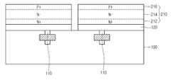
실시예에 따른 이미지센서는 배선(110)을 포함하는 회로(circuitry)(미도시)가 형성된 제1 기판(100); 상기 배선(110)과 선택적으로 접촉하도록 상기 제1 기판(100) 상에 형성된 실리콘층(120); 및 상기 실리콘층(120)과 접촉하면서 상기 제1 기판(100)과 본딩되고 상기 배선(110)과 전기적으로 연결되도록 형성된 포토다이오드(210);를 포함할 수 있다.The image sensor according to the embodiment includes a
또한, 상기 실리콘층(120)은 비정질층 또는 폴리실리콘층, 단결정실리콘층일 수 있으며, 결과적으로 수직형의 포토다이오드를 채용하면서 포토다이오드와 회로 사이에 포토다이오드와 결합력이 높은 실리콘층이 개재되어 포토다이오드와 회로 간의 물리적, 전기적 접촉력을 향상시킬 수 있다.In addition, the
예를 들어, 상기 포토다이오드가 형성되는 결정형 반도체층이 실리콘 결정질이고, 상기 실리콘층이 비정질 실리콘, 폴리실리콘층, 단결정실리콘층인 경우에 Si-Si 결합에 의해 제1 기판(100)과 제2 기판(200)의 결합력을 높일 수 있다.For example, when the crystalline semiconductor layer on which the photodiode is formed is silicon crystalline, and the silicon layer is amorphous silicon, polysilicon layer, or monocrystalline silicon layer, the
실시예에서 상기 실리콘층(120)은 약 100Å 내지 1,000Å의 두께로 형성됨으로써 제1 기판(100)과 제2 기판(200)의 결합층으로서 역할을 적절히 수행할 수 있다.In an exemplary embodiment, the
실시예에서 상기 결정형 반도체층(210a)(도 3 참조)은 단결층 반도체층일 수 있으나 이에 한정되는 것이 아니며, 다결정 반도체층일 수도 있다.In an embodiment, the
상기 제1 기판(100)의 회로(circuitry)는 미도시 되어 있으나, CIS의 경우 회로(circuitry)가 4개의 트랜지스터(4 Tr CIS)의 경우에 한정되는 것이 아니며, 1 Tr CIS, 3 Tr CIS, 5 Tr CIS 또는 1.5 Tr CIS(트랜지스터 공유 CIS) 등에도 적용이 가능하다.Although the circuit of the
또한, 제1 기판(100)에 형성된 배선(110)은 메탈(미도시)과 플러그(미도시)를 포함할 수 있다. 상기 배선(110) 중 최상부가 포토다이오드의 하부전극의 역할을 할 수 있다.In addition, the
다음으로 상기 포토다이오드(210)는 결정형 반도체층(210a)(도 4 참조) 내에 형성된 제1 도전형 전도층(214) 및 상기 제1 도전형 전도층(214) 상의 상기 결정형 반도체층 내에 형성된 제2 도전형 전도층(216)을 포함할 수 있다. 예를 들어, 상기 포토다이오드(210)는 상기 결정형 반도체층(210a) 내에 형성된 저농도 N형 전도층(214) 및 상기 저농도 N형 전도층(214) 상의 상기 결정형 반도체층 내에 형성된 고농도 P형 전도층(216)을 포함할 수 있으나, 이에 한정되는 것은 아니다. 즉, 제1 도전형은 N형에 한정되는 것이 아니며 P형 일 수도 있다.Next, the
또한, 실시예는 상기 제1 도전형 전도층(214) 하측에 고농도 제1 도전형 전도층(212)을 더 형성할 수 있다. 예를들어, 상기 고농도 제1 도전형 전도층(212)은 N+층으로 오믹컨택에 기여할 수 있다.In an embodiment, the first conductive type
실시예는 상기 포토다이오드(210) 상에 탑메탈(미도시)을 더 형성할 수 있고, 컬러필터(미도시)도 더 형성할 수 있다.In an embodiment, a top metal (not shown) may be further formed on the
실시예에서 상기 포토다이오드(210)는 픽셀마다 절연층(미도시)에 의해 분리될 수 있다.In an embodiment, the
도 2 내지 도 8은 실시예에 따른 이미지센서의 제조방법의 공정단면도이다.2 to 8 are process cross-sectional views of a method of manufacturing the image sensor according to the embodiment.
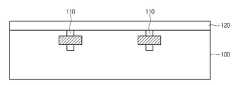
우선, 도 2와 같이 배선(110)과 회로(circuitry)(미도시)가 형성된 제1 기판(100)을 준비한다. 상기 제1 기판(100)의 회로(circuitry)는 미도시 되어 있으나, CIS의 경우 회로(circuitry)가 4개의 트랜지스터(4 Tr CIS)의 경우에 한정되는 것이 아니다.First, as shown in FIG. 2, a
또한, 제1 기판(100)에 형성된 배선(110)은 메탈(미도시)과 플러그(미도시)를 포함할 수 있다.In addition, the
다음으로, 상기 제1 기판(100) 상에 상기 배선(110)과 선택적으로 접촉하도록 실리콘층(120)을 형성한다.Next, the
상기 실리콘층(120)은 비정질층 또는 폴리실리콘층, 단결정실리콘층일 수 있으며, 결과적으로 수직형의 포토다이오드를 채용하면서 포토다이오드와 회로 사이에 포토다이오드와 결합력이 높은 실리콘층이 개재되어 포토다이오드와 회로 간의 물리적, 전기적 접촉력을 향상시킬 수 있다.The
예를 들어, 상기 포토다이오드가 형성되는 결정형 반도체층이 실리콘 결정질이고, 상기 실리콘층이 비정질 실리콘, 폴리실리콘층, 단결정실리콘층인 경우에 Si-Si 결합에 의해 제1 기판(100)과 제2 기판(200)의 결합력을 높일 수 있다.For example, when the crystalline semiconductor layer on which the photodiode is formed is silicon crystalline, and the silicon layer is amorphous silicon, polysilicon layer, or monocrystalline silicon layer, the
실시예에서 상기 실리콘층(120)은 약 100Å 내지 1,000Å의 두께로 형성됨으로써 제1 기판(100)과 제2 기판(200)의 결합층으로서 역할을 적절히 수행할 수 있다.In an exemplary embodiment, the
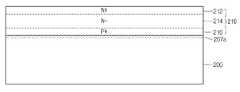
다음으로, 도 3과 같이 제2 기판(200) 상에 결정형 반도체층(crystalline semiconductor layer)(210a)을 형성한다. 이러한 결정형 반도체층(210a)에 포토다이오드가 형성됨으로써 포토다이오드 내의 디펙트를 방지할 수 있다.Next, as shown in FIG. 3, a
예를 들어, 상기 제2 기판(200) 상에 에패택시얼에 의해 결정형 반도체층(201a)을 형성한다. 이후, 제2 기판(200)과 결정형 반도체층(201a)의 경계에 수소이온을 주입하여 수소이온 주입층(207a)을 형성한다.For example, the crystalline semiconductor layer 201a is formed on the
다음으로, 도 4와 같이 결정형 반도체층(201a)에 이온주입에 의해 포토다이오드(210)를 형성한다.Next, as shown in FIG. 4, the
예를 들어, 상기 결정형 반도체층(210a) 하부에 제2 도전형 전도층(216)을 형성한다. 예를 들어, 상기 결정형 반도체층(210a) 하부에 마스크 없이 블랭킷으로 제2 기판(200) 전면에 이온주입하여 고농도 P형 전도층(216)을 형성할 수 있다. 예를 들어, 상기 제2 도전형 전도층(216)은 약 0.5 ㎛ 이내의 졍션뎁스(junction depth)로 형성될 수 있다.For example, a second conductivity type
이후, 상기 제2 도전형 전도층(216) 상부에 제1 도전형 전도층(214)을 형성한다. 예를 들어, 상기 2 도전형 전도층(216)의 상부에 마스크 없이 블랭킷으로 제2 기판(200) 전면에 이온주입하여 저농도 N형 전도층(214)을 형성할 수 있다. 예를 들어, 상기 저농도 제1 도전형 전도층(214)은 약 1.0~2.0 ㎛의 졍션뎁스(junction depth)로 형성될 수 있다.Thereafter, a first conductivity type
또한, 실시예는 상기 제1 도전형 전도층(214) 상측에 고농도 제1 도전형 전도층(212)을 더 형성할 수 있다. 예를 들어, 상기 고농도 제1 도전형 전도층(212)은 N+층으로 형성함으로써 오믹컨택에 기여할 수 있다.In an embodiment, the first conductive type
그 다음으로, 도 5와 같이 상기 포토다이오드(210)와 상기 실리콘층(120)이 접촉하도록 상기 제1 기판(100)과 상기 제2 기판(200)을 본딩(bonding)한다. 예를 들어, 상기 제1 기판(100)과 제2 기판(200)을 본딩하기 전에 플라즈마에 의한 액티베이션에 의해 본딩되는 면의 표면에너지를 높임으로써 본딩을 진행할 수 있다.Next, as illustrated in FIG. 5, the
다음으로, 도 6과 같이 제2 기판(200)에 열처리를 통해 수소이온 주입층(207a)이 수소기체층(207)으로 변하게 할 수 있다.Next, as illustrated in FIG. 6, the hydrogen
다음으로, 도 7과 같이 수소기체층(207)을 기준으로 제2 기판(200)을 하측을 용이하게 제거하여 포토다이오드(210)가 노출되도록 할 수 있다.Next, as illustrated in FIG. 7, the lower side of the
다음으로, 도 8과 같이 포토다이오드(210)를 픽셀별로 분리하는 식각을 진행 하고, 절연층(미도시)으로 식각된 부분을 채울 수 있다.Next, as shown in FIG. 8, the etching process of separating the
이후, 상부전극(미도시), 컬러필터(미도시) 등의 공정을 진행할 수 있다.Thereafter, a process of an upper electrode (not shown), a color filter (not shown), and the like may be performed.
실시예에 따른 이미지센서의 제조방법에 의하면 회로(circuitry)와 포토다이오드의 수직형 집적을 제공할 수 있다.According to the manufacturing method of the image sensor according to the embodiment it can provide a vertical integration of the circuit (circuitry) and the photodiode.
또한, 실시예에 의하면 수직형의 포토다이오드를 채용하면서 포토다이오드와 회로 사이에 실리콘층을 삽입함으로써 포토다이오드와 회로 간의 물리적, 전기적 접촉력을 향상시킬 수 있다.In addition, according to the embodiment, the physical and electrical contact force between the photodiode and the circuit can be improved by inserting a silicon layer between the photodiode and the circuit while employing the vertical photodiode.
또한, 실시예에 의하면 포토다이오드가 회로(circuitry)의 상측에 위치하는 수직형의 포토다이오드를 채용하면서 포토다이오드를 결정형 반도체층 내에 형성함으로써 포토다이오드 내의 디펙트를 방지할 수 있다.Further, according to the embodiment, it is possible to prevent defects in the photodiode by forming the photodiode in the crystalline semiconductor layer while employing a vertical photodiode positioned above the circuit.
본 발명은 기재된 실시예 및 도면에 의해 한정되는 것이 아니고, 청구항의 권리범위에 속하는 범위 안에서 다양한 다른 실시예가 가능하다.The present invention is not limited to the described embodiments and drawings, and various other embodiments are possible within the scope of the claims.
도 1은 실시예에 따른 이미지센서의 단면도.1 is a cross-sectional view of an image sensor according to an embodiment.
도 2 내지 도 8은 실시예에 따른 이미지센서의 제조방법의 공정단면도.2 to 8 are process cross-sectional views of the manufacturing method of the image sensor according to the embodiment.
Claims (7)
Translated fromKoreanPriority Applications (3)
| Application Number | Priority Date | Filing Date | Title |
|---|---|---|---|
| KR1020070139371AKR100883026B1 (en) | 2007-12-27 | 2007-12-27 | Image sensor and manufacturing method |
| CN2008101764750ACN101471355B (en) | 2007-12-27 | 2008-11-13 | Image sensor and method for manufacturing the sensor |
| US12/344,438US8080825B2 (en) | 2007-12-27 | 2008-12-26 | Image sensor and method for manufacturing the same |
Applications Claiming Priority (1)
| Application Number | Priority Date | Filing Date | Title |
|---|---|---|---|
| KR1020070139371AKR100883026B1 (en) | 2007-12-27 | 2007-12-27 | Image sensor and manufacturing method |
Publications (1)
| Publication Number | Publication Date |
|---|---|
| KR100883026B1true KR100883026B1 (en) | 2009-02-12 |
Family
ID=40681437
Family Applications (1)
| Application Number | Title | Priority Date | Filing Date |
|---|---|---|---|
| KR1020070139371AExpired - Fee RelatedKR100883026B1 (en) | 2007-12-27 | 2007-12-27 | Image sensor and manufacturing method |
Country Status (3)
| Country | Link |
|---|---|
| US (1) | US8080825B2 (en) |
| KR (1) | KR100883026B1 (en) |
| CN (1) | CN101471355B (en) |
Families Citing this family (172)
| Publication number | Priority date | Publication date | Assignee | Title |
|---|---|---|---|---|
| US10043781B2 (en) | 2009-10-12 | 2018-08-07 | Monolithic 3D Inc. | 3D semiconductor device and structure |
| US10388863B2 (en) | 2009-10-12 | 2019-08-20 | Monolithic 3D Inc. | 3D memory device and structure |
| US10366970B2 (en) | 2009-10-12 | 2019-07-30 | Monolithic 3D Inc. | 3D semiconductor device and structure |
| US10157909B2 (en) | 2009-10-12 | 2018-12-18 | Monolithic 3D Inc. | 3D semiconductor device and structure |
| US12027518B1 (en) | 2009-10-12 | 2024-07-02 | Monolithic 3D Inc. | 3D semiconductor devices and structures with metal layers |
| US11984445B2 (en) | 2009-10-12 | 2024-05-14 | Monolithic 3D Inc. | 3D semiconductor devices and structures with metal layers |
| US10910364B2 (en) | 2009-10-12 | 2021-02-02 | Monolitaic 3D Inc. | 3D semiconductor device |
| US11374118B2 (en) | 2009-10-12 | 2022-06-28 | Monolithic 3D Inc. | Method to form a 3D integrated circuit |
| US11018133B2 (en) | 2009-10-12 | 2021-05-25 | Monolithic 3D Inc. | 3D integrated circuit |
| US10354995B2 (en) | 2009-10-12 | 2019-07-16 | Monolithic 3D Inc. | Semiconductor memory device and structure |
| US10217667B2 (en) | 2011-06-28 | 2019-02-26 | Monolithic 3D Inc. | 3D semiconductor device, fabrication method and system |
| US10497713B2 (en) | 2010-11-18 | 2019-12-03 | Monolithic 3D Inc. | 3D semiconductor memory device and structure |
| US12362219B2 (en) | 2010-11-18 | 2025-07-15 | Monolithic 3D Inc. | 3D semiconductor memory device and structure |
| US11482440B2 (en) | 2010-12-16 | 2022-10-25 | Monolithic 3D Inc. | 3D semiconductor device and structure with a built-in test circuit for repairing faulty circuits |
| US11257867B1 (en) | 2010-10-11 | 2022-02-22 | Monolithic 3D Inc. | 3D semiconductor device and structure with oxide bonds |
| US11227897B2 (en) | 2010-10-11 | 2022-01-18 | Monolithic 3D Inc. | Method for producing a 3D semiconductor memory device and structure |
| US11024673B1 (en) | 2010-10-11 | 2021-06-01 | Monolithic 3D Inc. | 3D semiconductor device and structure |
| US11469271B2 (en) | 2010-10-11 | 2022-10-11 | Monolithic 3D Inc. | Method to produce 3D semiconductor devices and structures with memory |
| US10290682B2 (en) | 2010-10-11 | 2019-05-14 | Monolithic 3D Inc. | 3D IC semiconductor device and structure with stacked memory |
| US11158674B2 (en) | 2010-10-11 | 2021-10-26 | Monolithic 3D Inc. | Method to produce a 3D semiconductor device and structure |
| US10896931B1 (en) | 2010-10-11 | 2021-01-19 | Monolithic 3D Inc. | 3D semiconductor device and structure |
| US11600667B1 (en) | 2010-10-11 | 2023-03-07 | Monolithic 3D Inc. | Method to produce 3D semiconductor devices and structures with memory |
| US11018191B1 (en) | 2010-10-11 | 2021-05-25 | Monolithic 3D Inc. | 3D semiconductor device and structure |
| US11315980B1 (en) | 2010-10-11 | 2022-04-26 | Monolithic 3D Inc. | 3D semiconductor device and structure with transistors |
| US11855114B2 (en) | 2010-10-13 | 2023-12-26 | Monolithic 3D Inc. | Multilevel semiconductor device and structure with image sensors and wafer bonding |
| US11605663B2 (en) | 2010-10-13 | 2023-03-14 | Monolithic 3D Inc. | Multilevel semiconductor device and structure with image sensors and wafer bonding |
| US12094892B2 (en) | 2010-10-13 | 2024-09-17 | Monolithic 3D Inc. | 3D micro display device and structure |
| US11164898B2 (en) | 2010-10-13 | 2021-11-02 | Monolithic 3D Inc. | Multilevel semiconductor device and structure |
| US10998374B1 (en) | 2010-10-13 | 2021-05-04 | Monolithic 3D Inc. | Multilevel semiconductor device and structure |
| US11855100B2 (en) | 2010-10-13 | 2023-12-26 | Monolithic 3D Inc. | Multilevel semiconductor device and structure with oxide bonding |
| US11063071B1 (en) | 2010-10-13 | 2021-07-13 | Monolithic 3D Inc. | Multilevel semiconductor device and structure with waveguides |
| US12360310B2 (en) | 2010-10-13 | 2025-07-15 | Monolithic 3D Inc. | Multilevel semiconductor device and structure with oxide bonding |
| US11869915B2 (en) | 2010-10-13 | 2024-01-09 | Monolithic 3D Inc. | Multilevel semiconductor device and structure with image sensors and wafer bonding |
| US11404466B2 (en) | 2010-10-13 | 2022-08-02 | Monolithic 3D Inc. | Multilevel semiconductor device and structure with image sensors |
| US10679977B2 (en) | 2010-10-13 | 2020-06-09 | Monolithic 3D Inc. | 3D microdisplay device and structure |
| US11043523B1 (en) | 2010-10-13 | 2021-06-22 | Monolithic 3D Inc. | Multilevel semiconductor device and structure with image sensors |
| US11437368B2 (en) | 2010-10-13 | 2022-09-06 | Monolithic 3D Inc. | Multilevel semiconductor device and structure with oxide bonding |
| US9941319B2 (en)* | 2010-10-13 | 2018-04-10 | Monolithic 3D Inc. | Semiconductor and optoelectronic methods and devices |
| US11163112B2 (en) | 2010-10-13 | 2021-11-02 | Monolithic 3D Inc. | Multilevel semiconductor device and structure with electromagnetic modulators |
| US10833108B2 (en) | 2010-10-13 | 2020-11-10 | Monolithic 3D Inc. | 3D microdisplay device and structure |
| US11929372B2 (en) | 2010-10-13 | 2024-03-12 | Monolithic 3D Inc. | Multilevel semiconductor device and structure with image sensors and wafer bonding |
| US11984438B2 (en) | 2010-10-13 | 2024-05-14 | Monolithic 3D Inc. | Multilevel semiconductor device and structure with oxide bonding |
| US11133344B2 (en) | 2010-10-13 | 2021-09-28 | Monolithic 3D Inc. | Multilevel semiconductor device and structure with image sensors |
| US10978501B1 (en) | 2010-10-13 | 2021-04-13 | Monolithic 3D Inc. | Multilevel semiconductor device and structure with waveguides |
| US11327227B2 (en) | 2010-10-13 | 2022-05-10 | Monolithic 3D Inc. | Multilevel semiconductor device and structure with electromagnetic modulators |
| US12080743B2 (en) | 2010-10-13 | 2024-09-03 | Monolithic 3D Inc. | Multilevel semiconductor device and structure with image sensors and wafer bonding |
| US11694922B2 (en) | 2010-10-13 | 2023-07-04 | Monolithic 3D Inc. | Multilevel semiconductor device and structure with oxide bonding |
| US10943934B2 (en) | 2010-10-13 | 2021-03-09 | Monolithic 3D Inc. | Multilevel semiconductor device and structure |
| US11569117B2 (en) | 2010-11-18 | 2023-01-31 | Monolithic 3D Inc. | 3D semiconductor device and structure with single-crystal layers |
| US12125737B1 (en) | 2010-11-18 | 2024-10-22 | Monolithic 3D Inc. | 3D semiconductor device and structure with metal layers and memory cells |
| US11923230B1 (en) | 2010-11-18 | 2024-03-05 | Monolithic 3D Inc. | 3D semiconductor device and structure with bonding |
| US12100611B2 (en) | 2010-11-18 | 2024-09-24 | Monolithic 3D Inc. | Methods for producing a 3D semiconductor device and structure with memory cells and multiple metal layers |
| US11164770B1 (en) | 2010-11-18 | 2021-11-02 | Monolithic 3D Inc. | Method for producing a 3D semiconductor memory device and structure |
| US11018042B1 (en) | 2010-11-18 | 2021-05-25 | Monolithic 3D Inc. | 3D semiconductor memory device and structure |
| US11482439B2 (en) | 2010-11-18 | 2022-10-25 | Monolithic 3D Inc. | Methods for producing a 3D semiconductor memory device comprising charge trap junction-less transistors |
| US11521888B2 (en) | 2010-11-18 | 2022-12-06 | Monolithic 3D Inc. | 3D semiconductor device and structure with high-k metal gate transistors |
| US11004719B1 (en) | 2010-11-18 | 2021-05-11 | Monolithic 3D Inc. | Methods for producing a 3D semiconductor memory device and structure |
| US11495484B2 (en) | 2010-11-18 | 2022-11-08 | Monolithic 3D Inc. | 3D semiconductor devices and structures with at least two single-crystal layers |
| US11094576B1 (en) | 2010-11-18 | 2021-08-17 | Monolithic 3D Inc. | Methods for producing a 3D semiconductor memory device and structure |
| US11107721B2 (en) | 2010-11-18 | 2021-08-31 | Monolithic 3D Inc. | 3D semiconductor device and structure with NAND logic |
| US11854857B1 (en) | 2010-11-18 | 2023-12-26 | Monolithic 3D Inc. | Methods for producing a 3D semiconductor device and structure with memory cells and multiple metal layers |
| US11610802B2 (en) | 2010-11-18 | 2023-03-21 | Monolithic 3D Inc. | Method for producing a 3D semiconductor device and structure with single crystal transistors and metal gate electrodes |
| US11443971B2 (en) | 2010-11-18 | 2022-09-13 | Monolithic 3D Inc. | 3D semiconductor device and structure with memory |
| US11355381B2 (en) | 2010-11-18 | 2022-06-07 | Monolithic 3D Inc. | 3D semiconductor memory device and structure |
| US11508605B2 (en) | 2010-11-18 | 2022-11-22 | Monolithic 3D Inc. | 3D semiconductor memory device and structure |
| US11211279B2 (en) | 2010-11-18 | 2021-12-28 | Monolithic 3D Inc. | Method for processing a 3D integrated circuit and structure |
| US11355380B2 (en) | 2010-11-18 | 2022-06-07 | Monolithic 3D Inc. | Methods for producing 3D semiconductor memory device and structure utilizing alignment marks |
| US11121021B2 (en) | 2010-11-18 | 2021-09-14 | Monolithic 3D Inc. | 3D semiconductor device and structure |
| US11784082B2 (en) | 2010-11-18 | 2023-10-10 | Monolithic 3D Inc. | 3D semiconductor device and structure with bonding |
| US12144190B2 (en) | 2010-11-18 | 2024-11-12 | Monolithic 3D Inc. | 3D semiconductor device and structure with bonding and memory cells preliminary class |
| US11031275B2 (en) | 2010-11-18 | 2021-06-08 | Monolithic 3D Inc. | 3D semiconductor device and structure with memory |
| US11862503B2 (en) | 2010-11-18 | 2024-01-02 | Monolithic 3D Inc. | Method for producing a 3D semiconductor device and structure with memory cells and multiple metal layers |
| US11901210B2 (en) | 2010-11-18 | 2024-02-13 | Monolithic 3D Inc. | 3D semiconductor device and structure with memory |
| US12033884B2 (en) | 2010-11-18 | 2024-07-09 | Monolithic 3D Inc. | Methods for producing a 3D semiconductor device and structure with memory cells and multiple metal layers |
| US11615977B2 (en) | 2010-11-18 | 2023-03-28 | Monolithic 3D Inc. | 3D semiconductor memory device and structure |
| US11735462B2 (en) | 2010-11-18 | 2023-08-22 | Monolithic 3D Inc. | 3D semiconductor device and structure with single-crystal layers |
| US11804396B2 (en) | 2010-11-18 | 2023-10-31 | Monolithic 3D Inc. | Methods for producing a 3D semiconductor device and structure with memory cells and multiple metal layers |
| US12136562B2 (en) | 2010-11-18 | 2024-11-05 | Monolithic 3D Inc. | 3D semiconductor device and structure with single-crystal layers |
| US11482438B2 (en) | 2010-11-18 | 2022-10-25 | Monolithic 3D Inc. | Methods for producing a 3D semiconductor memory device and structure |
| US12272586B2 (en) | 2010-11-18 | 2025-04-08 | Monolithic 3D Inc. | 3D semiconductor memory device and structure with memory and metal layers |
| US12243765B2 (en) | 2010-11-18 | 2025-03-04 | Monolithic 3D Inc. | 3D semiconductor device and structure with metal layers and memory cells |
| US12154817B1 (en) | 2010-11-18 | 2024-11-26 | Monolithic 3D Inc. | Methods for producing a 3D semiconductor memory device and structure |
| US12068187B2 (en) | 2010-11-18 | 2024-08-20 | Monolithic 3D Inc. | 3D semiconductor device and structure with bonding and DRAM memory cells |
| US10388568B2 (en) | 2011-06-28 | 2019-08-20 | Monolithic 3D Inc. | 3D semiconductor device and system |
| US11164811B2 (en) | 2012-04-09 | 2021-11-02 | Monolithic 3D Inc. | 3D semiconductor device with isolation layers and oxide-to-oxide bonding |
| US11594473B2 (en) | 2012-04-09 | 2023-02-28 | Monolithic 3D Inc. | 3D semiconductor device and structure with metal layers and a connective path |
| US11694944B1 (en) | 2012-04-09 | 2023-07-04 | Monolithic 3D Inc. | 3D semiconductor device and structure with metal layers and a connective path |
| US11881443B2 (en) | 2012-04-09 | 2024-01-23 | Monolithic 3D Inc. | 3D semiconductor device and structure with metal layers and a connective path |
| US11616004B1 (en) | 2012-04-09 | 2023-03-28 | Monolithic 3D Inc. | 3D semiconductor device and structure with metal layers and a connective path |
| US11088050B2 (en) | 2012-04-09 | 2021-08-10 | Monolithic 3D Inc. | 3D semiconductor device with isolation layers |
| US10600888B2 (en) | 2012-04-09 | 2020-03-24 | Monolithic 3D Inc. | 3D semiconductor device |
| US11476181B1 (en) | 2012-04-09 | 2022-10-18 | Monolithic 3D Inc. | 3D semiconductor device and structure with metal layers |
| US11735501B1 (en) | 2012-04-09 | 2023-08-22 | Monolithic 3D Inc. | 3D semiconductor device and structure with metal layers and a connective path |
| US11410912B2 (en) | 2012-04-09 | 2022-08-09 | Monolithic 3D Inc. | 3D semiconductor device with vias and isolation layers |
| US8618865B1 (en)* | 2012-11-02 | 2013-12-31 | Palo Alto Research Center Incorporated | Capacitive imaging device with active pixels |
| US11018116B2 (en) | 2012-12-22 | 2021-05-25 | Monolithic 3D Inc. | Method to form a 3D semiconductor device and structure |
| US11063024B1 (en) | 2012-12-22 | 2021-07-13 | Monlithic 3D Inc. | Method to form a 3D semiconductor device and structure |
| US11784169B2 (en) | 2012-12-22 | 2023-10-10 | Monolithic 3D Inc. | 3D semiconductor device and structure with metal layers |
| US11961827B1 (en) | 2012-12-22 | 2024-04-16 | Monolithic 3D Inc. | 3D semiconductor device and structure with metal layers |
| US11217565B2 (en) | 2012-12-22 | 2022-01-04 | Monolithic 3D Inc. | Method to form a 3D semiconductor device and structure |
| US12051674B2 (en) | 2012-12-22 | 2024-07-30 | Monolithic 3D Inc. | 3D semiconductor device and structure with metal layers |
| US11967583B2 (en) | 2012-12-22 | 2024-04-23 | Monolithic 3D Inc. | 3D semiconductor device and structure with metal layers |
| US11309292B2 (en) | 2012-12-22 | 2022-04-19 | Monolithic 3D Inc. | 3D semiconductor device and structure with metal layers |
| US11916045B2 (en) | 2012-12-22 | 2024-02-27 | Monolithic 3D Inc. | 3D semiconductor device and structure with metal layers |
| US11430668B2 (en) | 2012-12-29 | 2022-08-30 | Monolithic 3D Inc. | 3D semiconductor device and structure with bonding |
| US11087995B1 (en) | 2012-12-29 | 2021-08-10 | Monolithic 3D Inc. | 3D semiconductor device and structure |
| US12249538B2 (en) | 2012-12-29 | 2025-03-11 | Monolithic 3D Inc. | 3D semiconductor device and structure including power distribution grids |
| US10600657B2 (en) | 2012-12-29 | 2020-03-24 | Monolithic 3D Inc | 3D semiconductor device and structure |
| US10903089B1 (en) | 2012-12-29 | 2021-01-26 | Monolithic 3D Inc. | 3D semiconductor device and structure |
| US11004694B1 (en) | 2012-12-29 | 2021-05-11 | Monolithic 3D Inc. | 3D semiconductor device and structure |
| US10892169B2 (en) | 2012-12-29 | 2021-01-12 | Monolithic 3D Inc. | 3D semiconductor device and structure |
| US11177140B2 (en) | 2012-12-29 | 2021-11-16 | Monolithic 3D Inc. | 3D semiconductor device and structure |
| US10115663B2 (en) | 2012-12-29 | 2018-10-30 | Monolithic 3D Inc. | 3D semiconductor device and structure |
| US10651054B2 (en) | 2012-12-29 | 2020-05-12 | Monolithic 3D Inc. | 3D semiconductor device and structure |
| US11430667B2 (en) | 2012-12-29 | 2022-08-30 | Monolithic 3D Inc. | 3D semiconductor device and structure with bonding |
| US12094965B2 (en) | 2013-03-11 | 2024-09-17 | Monolithic 3D Inc. | 3D semiconductor device and structure with metal layers and memory cells |
| US11935949B1 (en) | 2013-03-11 | 2024-03-19 | Monolithic 3D Inc. | 3D semiconductor device and structure with metal layers and memory cells |
| US8902663B1 (en) | 2013-03-11 | 2014-12-02 | Monolithic 3D Inc. | Method of maintaining a memory state |
| US10325651B2 (en) | 2013-03-11 | 2019-06-18 | Monolithic 3D Inc. | 3D semiconductor device with stacked memory |
| US11869965B2 (en) | 2013-03-11 | 2024-01-09 | Monolithic 3D Inc. | 3D semiconductor device and structure with metal layers and memory cells |
| US11088130B2 (en) | 2014-01-28 | 2021-08-10 | Monolithic 3D Inc. | 3D semiconductor device and structure |
| US11923374B2 (en) | 2013-03-12 | 2024-03-05 | Monolithic 3D Inc. | 3D semiconductor device and structure with metal layers |
| US12100646B2 (en) | 2013-03-12 | 2024-09-24 | Monolithic 3D Inc. | 3D semiconductor device and structure with metal layers |
| US11398569B2 (en) | 2013-03-12 | 2022-07-26 | Monolithic 3D Inc. | 3D semiconductor device and structure |
| US10840239B2 (en) | 2014-08-26 | 2020-11-17 | Monolithic 3D Inc. | 3D semiconductor device and structure |
| US10224279B2 (en) | 2013-03-15 | 2019-03-05 | Monolithic 3D Inc. | Semiconductor device and structure |
| US11574109B1 (en) | 2013-04-15 | 2023-02-07 | Monolithic 3D Inc | Automation methods for 3D integrated circuits and devices |
| US11270055B1 (en) | 2013-04-15 | 2022-03-08 | Monolithic 3D Inc. | Automation for monolithic 3D devices |
| US11030371B2 (en) | 2013-04-15 | 2021-06-08 | Monolithic 3D Inc. | Automation for monolithic 3D devices |
| US11720736B2 (en) | 2013-04-15 | 2023-08-08 | Monolithic 3D Inc. | Automation methods for 3D integrated circuits and devices |
| US9021414B1 (en) | 2013-04-15 | 2015-04-28 | Monolithic 3D Inc. | Automation for monolithic 3D devices |
| US11487928B2 (en) | 2013-04-15 | 2022-11-01 | Monolithic 3D Inc. | Automation for monolithic 3D devices |
| US11341309B1 (en) | 2013-04-15 | 2022-05-24 | Monolithic 3D Inc. | Automation for monolithic 3D devices |
| US11031394B1 (en) | 2014-01-28 | 2021-06-08 | Monolithic 3D Inc. | 3D semiconductor device and structure |
| US11107808B1 (en) | 2014-01-28 | 2021-08-31 | Monolithic 3D Inc. | 3D semiconductor device and structure |
| US10297586B2 (en) | 2015-03-09 | 2019-05-21 | Monolithic 3D Inc. | Methods for processing a 3D semiconductor device |
| US12094829B2 (en) | 2014-01-28 | 2024-09-17 | Monolithic 3D Inc. | 3D semiconductor device and structure |
| US10101373B2 (en) | 2014-04-21 | 2018-10-16 | Palo Alto Research Center Incorporated | Capacitive imaging device with active pixels and method |
| US10381328B2 (en) | 2015-04-19 | 2019-08-13 | Monolithic 3D Inc. | Semiconductor device and structure |
| US11056468B1 (en) | 2015-04-19 | 2021-07-06 | Monolithic 3D Inc. | 3D semiconductor device and structure |
| US10825779B2 (en) | 2015-04-19 | 2020-11-03 | Monolithic 3D Inc. | 3D semiconductor device and structure |
| US11011507B1 (en) | 2015-04-19 | 2021-05-18 | Monolithic 3D Inc. | 3D semiconductor device and structure |
| US11956952B2 (en) | 2015-08-23 | 2024-04-09 | Monolithic 3D Inc. | Semiconductor memory device and structure |
| US11978731B2 (en) | 2015-09-21 | 2024-05-07 | Monolithic 3D Inc. | Method to produce a multi-level semiconductor memory device and structure |
| US11937422B2 (en) | 2015-11-07 | 2024-03-19 | Monolithic 3D Inc. | Semiconductor memory device and structure |
| US12178055B2 (en) | 2015-09-21 | 2024-12-24 | Monolithic 3D Inc. | 3D semiconductor memory devices and structures |
| US11114427B2 (en) | 2015-11-07 | 2021-09-07 | Monolithic 3D Inc. | 3D semiconductor processor and memory device and structure |
| US12250830B2 (en) | 2015-09-21 | 2025-03-11 | Monolithic 3D Inc. | 3D semiconductor memory devices and structures |
| US12100658B2 (en) | 2015-09-21 | 2024-09-24 | Monolithic 3D Inc. | Method to produce a 3D multilayer semiconductor device and structure |
| CN108401468A (en) | 2015-09-21 | 2018-08-14 | 莫诺利特斯3D有限公司 | 3D semiconductor devices and structures |
| US10522225B1 (en) | 2015-10-02 | 2019-12-31 | Monolithic 3D Inc. | Semiconductor device with non-volatile memory |
| US11991884B1 (en) | 2015-10-24 | 2024-05-21 | Monolithic 3D Inc. | 3D semiconductor device and structure with logic and memory |
| US10418369B2 (en) | 2015-10-24 | 2019-09-17 | Monolithic 3D Inc. | Multi-level semiconductor memory device and structure |
| US12219769B2 (en) | 2015-10-24 | 2025-02-04 | Monolithic 3D Inc. | 3D semiconductor device and structure with logic and memory |
| US11296115B1 (en) | 2015-10-24 | 2022-04-05 | Monolithic 3D Inc. | 3D semiconductor device and structure |
| US12035531B2 (en) | 2015-10-24 | 2024-07-09 | Monolithic 3D Inc. | 3D semiconductor device and structure with logic and memory |
| US12120880B1 (en) | 2015-10-24 | 2024-10-15 | Monolithic 3D Inc. | 3D semiconductor device and structure with logic and memory |
| US12016181B2 (en) | 2015-10-24 | 2024-06-18 | Monolithic 3D Inc. | 3D semiconductor device and structure with logic and memory |
| US10847540B2 (en) | 2015-10-24 | 2020-11-24 | Monolithic 3D Inc. | 3D semiconductor memory device and structure |
| US11114464B2 (en) | 2015-10-24 | 2021-09-07 | Monolithic 3D Inc. | 3D semiconductor device and structure |
| US11869591B2 (en) | 2016-10-10 | 2024-01-09 | Monolithic 3D Inc. | 3D memory devices and structures with control circuits |
| US11251149B2 (en) | 2016-10-10 | 2022-02-15 | Monolithic 3D Inc. | 3D memory device and structure |
| US12225704B2 (en) | 2016-10-10 | 2025-02-11 | Monolithic 3D Inc. | 3D memory devices and structures with memory arrays and metal layers |
| US11812620B2 (en) | 2016-10-10 | 2023-11-07 | Monolithic 3D Inc. | 3D DRAM memory devices and structures with control circuits |
| US11711928B2 (en) | 2016-10-10 | 2023-07-25 | Monolithic 3D Inc. | 3D memory devices and structures with control circuits |
| US11329059B1 (en) | 2016-10-10 | 2022-05-10 | Monolithic 3D Inc. | 3D memory devices and structures with thinned single crystal substrates |
| US11930648B1 (en) | 2016-10-10 | 2024-03-12 | Monolithic 3D Inc. | 3D memory devices and structures with metal layers |
| US10892016B1 (en) | 2019-04-08 | 2021-01-12 | Monolithic 3D Inc. | 3D memory semiconductor devices and structures |
| US11158652B1 (en) | 2019-04-08 | 2021-10-26 | Monolithic 3D Inc. | 3D memory semiconductor devices and structures |
| US11018156B2 (en) | 2019-04-08 | 2021-05-25 | Monolithic 3D Inc. | 3D memory semiconductor devices and structures |
| US11296106B2 (en) | 2019-04-08 | 2022-04-05 | Monolithic 3D Inc. | 3D memory semiconductor devices and structures |
| US11763864B2 (en) | 2019-04-08 | 2023-09-19 | Monolithic 3D Inc. | 3D memory semiconductor devices and structures with bit-line pillars |
Citations (3)
| Publication number | Priority date | Publication date | Assignee | Title |
|---|---|---|---|---|
| KR20050062000A (en)* | 2003-12-19 | 2005-06-23 | 매그나칩 반도체 유한회사 | Image sensor and method of manufacturing the same |
| KR20050117594A (en)* | 2000-06-23 | 2005-12-15 | 주식회사 하이닉스반도체 | Manufacturing method for semiconductor device |
| KR20060120260A (en)* | 2006-08-25 | 2006-11-24 | 에스.오.아이. 테크 실리콘 온 인슐레이터 테크놀로지스 | Photodetector |
Family Cites Families (2)
| Publication number | Priority date | Publication date | Assignee | Title |
|---|---|---|---|---|
| US6791130B2 (en)* | 2002-08-27 | 2004-09-14 | E-Phocus, Inc. | Photoconductor-on-active-pixel (POAP) sensor utilizing a multi-layered radiation absorbing structure |
| KR100856941B1 (en)* | 2008-01-07 | 2008-09-04 | 주식회사 동부하이텍 | Image sensor and manufacturing method |
- 2007
- 2007-12-27KRKR1020070139371Apatent/KR100883026B1/ennot_activeExpired - Fee Related
- 2008
- 2008-11-13CNCN2008101764750Apatent/CN101471355B/ennot_activeExpired - Fee Related
- 2008-12-26USUS12/344,438patent/US8080825B2/ennot_activeExpired - Fee Related
Patent Citations (3)
| Publication number | Priority date | Publication date | Assignee | Title |
|---|---|---|---|---|
| KR20050117594A (en)* | 2000-06-23 | 2005-12-15 | 주식회사 하이닉스반도체 | Manufacturing method for semiconductor device |
| KR20050062000A (en)* | 2003-12-19 | 2005-06-23 | 매그나칩 반도체 유한회사 | Image sensor and method of manufacturing the same |
| KR20060120260A (en)* | 2006-08-25 | 2006-11-24 | 에스.오.아이. 테크 실리콘 온 인슐레이터 테크놀로지스 | Photodetector |
Also Published As
| Publication number | Publication date |
|---|---|
| US20090166627A1 (en) | 2009-07-02 |
| CN101471355B (en) | 2012-08-29 |
| CN101471355A (en) | 2009-07-01 |
| US8080825B2 (en) | 2011-12-20 |
Similar Documents
| Publication | Publication Date | Title |
|---|---|---|
| KR100883026B1 (en) | Image sensor and manufacturing method | |
| KR100860141B1 (en) | Image sensor and manufacturing method | |
| KR100856941B1 (en) | Image sensor and manufacturing method | |
| KR100856942B1 (en) | Image sensor and manufacturing method | |
| JP2009065155A (en) | Image sensor | |
| US7884391B2 (en) | Image sensor and method for manufacturing the same | |
| KR100855404B1 (en) | Image sensor and manufacturing method | |
| JP2009065156A (en) | Manufacturing method of image sensor | |
| KR100855403B1 (en) | Image sensor and manufacturing method | |
| CN101383362A (en) | Image sensor and manufacturing method thereof | |
| US20090179242A1 (en) | Image sensor and method for manufacturing the same | |
| KR100863361B1 (en) | Image sensor and manufacturing method | |
| KR100882468B1 (en) | Image sensor and manufacturing method | |
| KR100849238B1 (en) | Image sensor and manufacturing method | |
| KR100936105B1 (en) | Image sensor and manufacturing method | |
| US20090114964A1 (en) | Image sensor and method for manufacturing the same | |
| JP2010098314A (en) | Image sensor and method of manufacturing the same | |
| KR100922922B1 (en) | Image Sensor and Method for Manufacturing thereof | |
| KR100877242B1 (en) | Image sensor and manufacturing method | |
| JP2010098312A (en) | Method of manufacturing image sensor | |
| JP2008270668A (en) | Solid-state imaging device and manufacturing method thereof | |
| KR100856949B1 (en) | Manufacturing Method of Image Sensor | |
| KR100898472B1 (en) | Method for Manufacturing Image Sensor | |
| KR20110078880A (en) | Manufacturing Method of Image Sensor | |
| CN101431091A (en) | Image sensor and method for manufacturing the same |
Legal Events
| Date | Code | Title | Description |
|---|---|---|---|
| A201 | Request for examination | ||
| PA0109 | Patent application | St.27 status event code:A-0-1-A10-A12-nap-PA0109 | |
| PA0201 | Request for examination | St.27 status event code:A-1-2-D10-D11-exm-PA0201 | |
| A302 | Request for accelerated examination | ||
| PA0302 | Request for accelerated examination | St.27 status event code:A-1-2-D10-D17-exm-PA0302 St.27 status event code:A-1-2-D10-D16-exm-PA0302 | |
| E902 | Notification of reason for refusal | ||
| PE0902 | Notice of grounds for rejection | St.27 status event code:A-1-2-D10-D21-exm-PE0902 | |
| T11-X000 | Administrative time limit extension requested | St.27 status event code:U-3-3-T10-T11-oth-X000 | |
| AMND | Amendment | ||
| P11-X000 | Amendment of application requested | St.27 status event code:A-2-2-P10-P11-nap-X000 | |
| P13-X000 | Application amended | St.27 status event code:A-2-2-P10-P13-nap-X000 | |
| E902 | Notification of reason for refusal | ||
| PE0902 | Notice of grounds for rejection | St.27 status event code:A-1-2-D10-D21-exm-PE0902 | |
| AMND | Amendment | ||
| P11-X000 | Amendment of application requested | St.27 status event code:A-2-2-P10-P11-nap-X000 | |
| P13-X000 | Application amended | St.27 status event code:A-2-2-P10-P13-nap-X000 | |
| E601 | Decision to refuse application | ||
| PE0601 | Decision on rejection of patent | St.27 status event code:N-2-6-B10-B15-exm-PE0601 | |
| J201 | Request for trial against refusal decision | ||
| PJ0201 | Trial against decision of rejection | St.27 status event code:A-3-3-V10-V11-apl-PJ0201 | |
| AMND | Amendment | ||
| P11-X000 | Amendment of application requested | St.27 status event code:A-2-2-P10-P11-nap-X000 | |
| P13-X000 | Application amended | St.27 status event code:A-2-2-P10-P13-nap-X000 | |
| PB0901 | Examination by re-examination before a trial | St.27 status event code:A-6-3-E10-E12-rex-PB0901 | |
| B701 | Decision to grant | ||
| PB0701 | Decision of registration after re-examination before a trial | St.27 status event code:A-3-4-F10-F13-rex-PB0701 | |
| GRNT | Written decision to grant | ||
| PR0701 | Registration of establishment | St.27 status event code:A-2-4-F10-F11-exm-PR0701 | |
| PR1002 | Payment of registration fee | St.27 status event code:A-2-2-U10-U11-oth-PR1002 Fee payment year number:1 | |
| PG1601 | Publication of registration | St.27 status event code:A-4-4-Q10-Q13-nap-PG1601 | |
| FPAY | Annual fee payment | Payment date:20120119 Year of fee payment:4 | |
| PR1001 | Payment of annual fee | St.27 status event code:A-4-4-U10-U11-oth-PR1001 Fee payment year number:4 | |
| LAPS | Lapse due to unpaid annual fee | ||
| PC1903 | Unpaid annual fee | St.27 status event code:A-4-4-U10-U13-oth-PC1903 Not in force date:20130204 Payment event data comment text:Termination Category : DEFAULT_OF_REGISTRATION_FEE | |
| PC1903 | Unpaid annual fee | St.27 status event code:N-4-6-H10-H13-oth-PC1903 Ip right cessation event data comment text:Termination Category : DEFAULT_OF_REGISTRATION_FEE Not in force date:20130204 | |
| PN2301 | Change of applicant | St.27 status event code:A-5-5-R10-R13-asn-PN2301 St.27 status event code:A-5-5-R10-R11-asn-PN2301 | |
| R18-X000 | Changes to party contact information recorded | St.27 status event code:A-5-5-R10-R18-oth-X000 | |
| P22-X000 | Classification modified | St.27 status event code:A-4-4-P10-P22-nap-X000 |