KR100882409B1 - Antireflection silicone resin, antireflection film material, antireflection film and pattern formation method using the same - Google Patents
Antireflection silicone resin, antireflection film material, antireflection film and pattern formation method using the sameDownload PDFInfo
- Publication number
- KR100882409B1 KR100882409B1KR1020040040028AKR20040040028AKR100882409B1KR 100882409 B1KR100882409 B1KR 100882409B1KR 1020040040028 AKR1020040040028 AKR 1020040040028AKR 20040040028 AKR20040040028 AKR 20040040028AKR 100882409 B1KR100882409 B1KR 100882409B1
- Authority
- KR
- South Korea
- Prior art keywords
- group
- film
- antireflection film
- substrate
- pattern
- Prior art date
- Legal status (The legal status is an assumption and is not a legal conclusion. Google has not performed a legal analysis and makes no representation as to the accuracy of the status listed.)
- Expired - Lifetime
Links
- 239000000463materialSubstances0.000titleclaimsabstractdescription76
- 238000000034methodMethods0.000titleclaimsabstractdescription49
- 229920002050silicone resinPolymers0.000titleclaimsabstractdescription22
- 230000007261regionalizationEffects0.000titleabstractdescription13
- 239000000758substrateSubstances0.000claimsabstractdescription74
- 238000005530etchingMethods0.000claimsabstractdescription53
- 239000002253acidSubstances0.000claimsabstractdescription40
- 229910008051Si-OHInorganic materials0.000claimsabstractdescription28
- 229910006358Si—OHInorganic materials0.000claimsabstractdescription28
- 239000003960organic solventSubstances0.000claimsabstractdescription27
- 239000006096absorbing agentSubstances0.000claimsabstractdescription20
- 229920005989resinPolymers0.000claimsabstractdescription18
- 239000011347resinSubstances0.000claimsabstractdescription18
- XUIMIQQOPSSXEZ-UHFFFAOYSA-NSiliconChemical compound[Si]XUIMIQQOPSSXEZ-UHFFFAOYSA-N0.000claimsabstractdescription17
- 229910052710siliconInorganic materials0.000claimsabstractdescription16
- 125000000962organic groupChemical group0.000claimsabstractdescription14
- 239000010703siliconSubstances0.000claimsabstractdescription8
- 229920002120photoresistant polymerPolymers0.000claimsdescription71
- 125000004432carbon atomChemical groupC*0.000claimsdescription32
- WGTYBPLFGIVFAS-UHFFFAOYSA-Mtetramethylammonium hydroxideChemical compound[OH-].C[N+](C)(C)CWGTYBPLFGIVFAS-UHFFFAOYSA-M0.000claimsdescription26
- 230000003667anti-reflective effectEffects0.000claimsdescription20
- 238000001459lithographyMethods0.000claimsdescription15
- 125000001997phenyl groupChemical group[H]C1=C([H])C([H])=C(*)C([H])=C1[H]0.000claimsdescription13
- 125000003545alkoxy groupChemical group0.000claimsdescription12
- 125000004435hydrogen atomChemical group[H]*0.000claimsdescription11
- 239000011248coating agentSubstances0.000claimsdescription9
- 238000000576coating methodMethods0.000claimsdescription9
- 125000001624naphthyl groupChemical group0.000claimsdescription8
- 238000009833condensationMethods0.000claimsdescription7
- 230000005494condensationEffects0.000claimsdescription7
- 239000000178monomerSubstances0.000claimsdescription7
- 230000003472neutralizing effectEffects0.000claimsdescription7
- 239000003795chemical substances by applicationSubstances0.000claimsdescription6
- 125000002887hydroxy groupChemical group[H]O*0.000claimsdescription6
- 125000003700epoxy groupChemical group0.000claimsdescription5
- 238000006460hydrolysis reactionMethods0.000claimsdescription5
- 125000005196alkyl carbonyloxy groupChemical group0.000claimsdescription3
- 230000007062hydrolysisEffects0.000claimsdescription3
- 150000001412aminesChemical class0.000claimsdescription2
- 125000005577anthracene groupChemical group0.000claimsdescription2
- 125000005843halogen groupChemical group0.000claimsdescription2
- 230000000873masking effectEffects0.000claimsdescription2
- CSJDCSCTVDEHRN-UHFFFAOYSA-Nmethane;molecular oxygenChemical compoundC.O=OCSJDCSCTVDEHRN-UHFFFAOYSA-N0.000abstractdescription7
- 238000012545processingMethods0.000abstractdescription5
- 230000002265preventionEffects0.000abstractdescription2
- 239000010408filmSubstances0.000description269
- -1perfluoroChemical group0.000description145
- XEKOWRVHYACXOJ-UHFFFAOYSA-NEthyl acetateChemical compoundCCOC(C)=OXEKOWRVHYACXOJ-UHFFFAOYSA-N0.000description51
- 239000000203mixtureSubstances0.000description51
- 229920000642polymerPolymers0.000description49
- QTBSBXVTEAMEQO-UHFFFAOYSA-NAcetic acidChemical compoundCC(O)=OQTBSBXVTEAMEQO-UHFFFAOYSA-N0.000description48
- 238000006243chemical reactionMethods0.000description46
- 239000007788liquidSubstances0.000description46
- OKKJLVBELUTLKV-UHFFFAOYSA-NMethanolChemical compoundOCOKKJLVBELUTLKV-UHFFFAOYSA-N0.000description40
- LLHKCFNBLRBOGN-UHFFFAOYSA-Npropylene glycol methyl ether acetateChemical compoundCOCC(C)OC(C)=OLLHKCFNBLRBOGN-UHFFFAOYSA-N0.000description28
- 238000005227gel permeation chromatographyMethods0.000description22
- XLYOFNOQVPJJNP-UHFFFAOYSA-NwaterSubstancesOXLYOFNOQVPJJNP-UHFFFAOYSA-N0.000description22
- 23800000164413C nuclear magnetic resonance spectroscopyMethods0.000description21
- 239000002585baseSubstances0.000description21
- WYURNTSHIVDZCO-UHFFFAOYSA-NTetrahydrofuranChemical compoundC1CCOC1WYURNTSHIVDZCO-UHFFFAOYSA-N0.000description20
- 230000015572biosynthetic processEffects0.000description19
- LFQSCWFLJHTTHZ-UHFFFAOYSA-NEthanolChemical compoundCCOLFQSCWFLJHTTHZ-UHFFFAOYSA-N0.000description18
- 150000001875compoundsChemical class0.000description18
- 239000007789gasSubstances0.000description18
- 238000010438heat treatmentMethods0.000description17
- 235000011054acetic acidNutrition0.000description16
- 238000007334copolymerization reactionMethods0.000description16
- 238000003786synthesis reactionMethods0.000description16
- 125000000217alkyl groupChemical group0.000description15
- 230000000052comparative effectEffects0.000description15
- 238000004132cross linkingMethods0.000description13
- 239000000243solutionSubstances0.000description13
- 229910021642ultra pure waterInorganic materials0.000description13
- 239000012498ultrapure waterSubstances0.000description13
- 238000005481NMR spectroscopyMethods0.000description12
- PPBRXRYQALVLMV-UHFFFAOYSA-NStyreneChemical compoundC=CC1=CC=CC=C1PPBRXRYQALVLMV-UHFFFAOYSA-N0.000description12
- 230000000694effectsEffects0.000description12
- 239000004793PolystyreneSubstances0.000description11
- 229920002223polystyrenePolymers0.000description11
- RTZKZFJDLAIYFH-UHFFFAOYSA-NDiethyl etherChemical compoundCCOCCRTZKZFJDLAIYFH-UHFFFAOYSA-N0.000description10
- 239000007864aqueous solutionSubstances0.000description10
- 125000003118aryl groupChemical group0.000description10
- 239000003054catalystSubstances0.000description10
- 125000002496methyl groupChemical group[H]C([H])([H])*0.000description10
- YLQBMQCUIZJEEH-UHFFFAOYSA-NtetrahydrofuranNatural productsC=1C=COC=1YLQBMQCUIZJEEH-UHFFFAOYSA-N0.000description10
- ZNOCGWVLWPVKAO-UHFFFAOYSA-Ntrimethoxy(phenyl)silaneChemical compoundCO[Si](OC)(OC)C1=CC=CC=C1ZNOCGWVLWPVKAO-UHFFFAOYSA-N0.000description10
- ARXJGSRGQADJSQ-UHFFFAOYSA-N1-methoxypropan-2-olChemical compoundCOCC(C)OARXJGSRGQADJSQ-UHFFFAOYSA-N0.000description9
- 229910004298SiO 2Inorganic materials0.000description9
- 238000001312dry etchingMethods0.000description9
- 239000011521glassSubstances0.000description9
- 238000004528spin coatingMethods0.000description8
- AFVFQIVMOAPDHO-UHFFFAOYSA-NMethanesulfonic acidChemical compoundCS(O)(=O)=OAFVFQIVMOAPDHO-UHFFFAOYSA-N0.000description7
- 125000002947alkylene groupChemical group0.000description7
- 238000011161developmentMethods0.000description7
- 230000018109developmental processEffects0.000description7
- QGZKDVFQNNGYKY-UHFFFAOYSA-NAmmoniaChemical compoundNQGZKDVFQNNGYKY-UHFFFAOYSA-N0.000description6
- VEXZGXHMUGYJMC-UHFFFAOYSA-NHydrochloric acidChemical compoundClVEXZGXHMUGYJMC-UHFFFAOYSA-N0.000description6
- BAPJBEWLBFYGME-UHFFFAOYSA-NMethyl acrylateChemical compoundCOC(=O)C=CBAPJBEWLBFYGME-UHFFFAOYSA-N0.000description6
- KWYUFKZDYYNOTN-UHFFFAOYSA-MPotassium hydroxideChemical compound[OH-].[K+]KWYUFKZDYYNOTN-UHFFFAOYSA-M0.000description6
- HEMHJVSKTPXQMS-UHFFFAOYSA-MSodium hydroxideChemical compound[OH-].[Na+]HEMHJVSKTPXQMS-UHFFFAOYSA-M0.000description6
- YXFVVABEGXRONW-UHFFFAOYSA-NTolueneChemical compoundCC1=CC=CC=C1YXFVVABEGXRONW-UHFFFAOYSA-N0.000description6
- ZMANZCXQSJIPKH-UHFFFAOYSA-NTriethylamineChemical compoundCCN(CC)CCZMANZCXQSJIPKH-UHFFFAOYSA-N0.000description6
- 239000003513alkaliSubstances0.000description6
- 125000003710aryl alkyl groupChemical group0.000description6
- KRKNYBCHXYNGOX-UHFFFAOYSA-Ncitric acidChemical compoundOC(=O)CC(O)(C(O)=O)CC(O)=OKRKNYBCHXYNGOX-UHFFFAOYSA-N0.000description6
- JHIVVAPYMSGYDF-UHFFFAOYSA-NcyclohexanoneChemical compoundO=C1CCCCC1JHIVVAPYMSGYDF-UHFFFAOYSA-N0.000description6
- XBDQKXXYIPTUBI-UHFFFAOYSA-NdimethylselenoniopropionateNatural productsCCC(O)=OXBDQKXXYIPTUBI-UHFFFAOYSA-N0.000description6
- 238000004519manufacturing processMethods0.000description6
- VLKZOEOYAKHREP-UHFFFAOYSA-Nn-HexaneChemical compoundCCCCCCVLKZOEOYAKHREP-UHFFFAOYSA-N0.000description6
- 125000001424substituent groupChemical group0.000description6
- BPSIOYPQMFLKFR-UHFFFAOYSA-Ntrimethoxy-[3-(oxiran-2-ylmethoxy)propyl]silaneChemical compoundCO[Si](OC)(OC)CCCOCC1CO1BPSIOYPQMFLKFR-UHFFFAOYSA-N0.000description6
- LIPRQQHINVWJCH-UHFFFAOYSA-N1-ethoxypropan-2-yl acetateChemical compoundCCOCC(C)OC(C)=OLIPRQQHINVWJCH-UHFFFAOYSA-N0.000description5
- OFOBLEOULBTSOW-UHFFFAOYSA-NPropanedioic acidNatural productsOC(=O)CC(O)=OOFOBLEOULBTSOW-UHFFFAOYSA-N0.000description5
- VYPSYNLAJGMNEJ-UHFFFAOYSA-NSilicium dioxideChemical compoundO=[Si]=OVYPSYNLAJGMNEJ-UHFFFAOYSA-N0.000description5
- NIXOWILDQLNWCW-UHFFFAOYSA-Nacrylic acid groupChemical groupC(C=C)(=O)ONIXOWILDQLNWCW-UHFFFAOYSA-N0.000description5
- 125000003342alkenyl groupChemical group0.000description5
- 239000000460chlorineSubstances0.000description5
- 229920001577copolymerPolymers0.000description5
- SBZXBUIDTXKZTM-UHFFFAOYSA-NdiglymeChemical compoundCOCCOCCOCSBZXBUIDTXKZTM-UHFFFAOYSA-N0.000description5
- 125000001495ethyl groupChemical group[H]C([H])([H])C([H])([H])*0.000description5
- 125000001449isopropyl groupChemical group[H]C([H])([H])C([H])(*)C([H])([H])[H]0.000description5
- 125000004108n-butyl groupChemical group[H]C([H])([H])C([H])([H])C([H])([H])C([H])([H])*0.000description5
- 150000003459sulfonic acid estersChemical class0.000description5
- 125000000999tert-butyl groupChemical group[H]C([H])([H])C(*)(C([H])([H])[H])C([H])([H])[H]0.000description5
- JOXIMZWYDAKGHI-UHFFFAOYSA-Ntoluene-4-sulfonic acidChemical compoundCC1=CC=C(S(O)(=O)=O)C=C1JOXIMZWYDAKGHI-UHFFFAOYSA-N0.000description5
- DQZNLOXENNXVAD-UHFFFAOYSA-Ntrimethoxy-[2-(7-oxabicyclo[4.1.0]heptan-4-yl)ethyl]silaneChemical compoundC1C(CC[Si](OC)(OC)OC)CCC2OC21DQZNLOXENNXVAD-UHFFFAOYSA-N0.000description5
- LEEANUDEDHYDTG-UHFFFAOYSA-N1,2-dimethoxypropaneChemical compoundCOCC(C)OCLEEANUDEDHYDTG-UHFFFAOYSA-N0.000description4
- GQHTUMJGOHRCHB-UHFFFAOYSA-N2,3,4,6,7,8,9,10-octahydropyrimido[1,2-a]azepineChemical compoundC1CCCCN2CCCN=C21GQHTUMJGOHRCHB-UHFFFAOYSA-N0.000description4
- XNWFRZJHXBZDAG-UHFFFAOYSA-N2-METHOXYETHANOLChemical compoundCOCCOXNWFRZJHXBZDAG-UHFFFAOYSA-N0.000description4
- ZNQVEEAIQZEUHB-UHFFFAOYSA-N2-ethoxyethanolChemical compoundCCOCCOZNQVEEAIQZEUHB-UHFFFAOYSA-N0.000description4
- YXHKONLOYHBTNS-UHFFFAOYSA-NDiazomethaneChemical classC=[N+]=[N-]YXHKONLOYHBTNS-UHFFFAOYSA-N0.000description4
- VZCYOOQTPOCHFL-OWOJBTEDSA-NFumaric acidChemical compoundOC(=O)\C=C\C(O)=OVZCYOOQTPOCHFL-OWOJBTEDSA-N0.000description4
- QAOWNCQODCNURD-UHFFFAOYSA-NSulfuric acidChemical compoundOS(O)(=O)=OQAOWNCQODCNURD-UHFFFAOYSA-N0.000description4
- 125000002777acetyl groupChemical group[H]C([H])([H])C(*)=O0.000description4
- 125000004429atomChemical group0.000description4
- WPYMKLBDIGXBTP-UHFFFAOYSA-Nbenzoic acidChemical compoundOC(=O)C1=CC=CC=C1WPYMKLBDIGXBTP-UHFFFAOYSA-N0.000description4
- 239000003431cross linking reagentSubstances0.000description4
- 125000006165cyclic alkyl groupChemical group0.000description4
- 125000000113cyclohexyl groupChemical group[H]C1([H])C([H])([H])C([H])([H])C([H])(*)C([H])([H])C1([H])[H]0.000description4
- 229940098779methanesulfonic acidDrugs0.000description4
- BDAGIHXWWSANSR-UHFFFAOYSA-Nmethanoic acidNatural productsOC=OBDAGIHXWWSANSR-UHFFFAOYSA-N0.000description4
- 125000000956methoxy groupChemical group[H]C([H])([H])O*0.000description4
- 125000001147pentyl groupChemical groupC(CCCC)*0.000description4
- VLTRZXGMWDSKGL-UHFFFAOYSA-Nperchloric acidChemical compoundOCl(=O)(=O)=OVLTRZXGMWDSKGL-UHFFFAOYSA-N0.000description4
- JGTNAGYHADQMCM-UHFFFAOYSA-Nperfluorobutanesulfonic acidChemical compoundOS(=O)(=O)C(F)(F)C(F)(F)C(F)(F)C(F)(F)FJGTNAGYHADQMCM-UHFFFAOYSA-N0.000description4
- XNGIFLGASWRNHJ-UHFFFAOYSA-Nphthalic acidChemical compoundOC(=O)C1=CC=CC=C1C(O)=OXNGIFLGASWRNHJ-UHFFFAOYSA-N0.000description4
- 238000006116polymerization reactionMethods0.000description4
- 125000001436propyl groupChemical group[H]C([*])([H])C([H])([H])C([H])([H])[H]0.000description4
- YGSDEFSMJLZEOE-UHFFFAOYSA-Nsalicylic acidChemical compoundOC(=O)C1=CC=CC=C1OYGSDEFSMJLZEOE-UHFFFAOYSA-N0.000description4
- 150000003839saltsChemical class0.000description4
- 125000002914sec-butyl groupChemical group[H]C([H])([H])C([H])([H])C([H])(*)C([H])([H])[H]0.000description4
- 238000012360testing methodMethods0.000description4
- VDZOOKBUILJEDG-UHFFFAOYSA-Mtetrabutylammonium hydroxideChemical compound[OH-].CCCC[N+](CCCC)(CCCC)CCCCVDZOOKBUILJEDG-UHFFFAOYSA-M0.000description4
- ITMCEJHCFYSIIV-UHFFFAOYSA-Ntriflic acidChemical compoundOS(=O)(=O)C(F)(F)FITMCEJHCFYSIIV-UHFFFAOYSA-N0.000description4
- LJHFIVQEAFAURQ-ZPUQHVIOSA-N(NE)-N-[(2E)-2-hydroxyiminoethylidene]hydroxylamineChemical classO\N=C\C=N\OLJHFIVQEAFAURQ-ZPUQHVIOSA-N0.000description3
- UUGLSEIATNSHRI-UHFFFAOYSA-N1,3,4,6-tetrakis(hydroxymethyl)-3a,6a-dihydroimidazo[4,5-d]imidazole-2,5-dioneChemical compoundOCN1C(=O)N(CO)C2C1N(CO)C(=O)N2COUUGLSEIATNSHRI-UHFFFAOYSA-N0.000description3
- JOLQKTGDSGKSKJ-UHFFFAOYSA-N1-ethoxypropan-2-olChemical compoundCCOCC(C)OJOLQKTGDSGKSKJ-UHFFFAOYSA-N0.000description3
- SMZOUWXMTYCWNB-UHFFFAOYSA-N2-(2-methoxy-5-methylphenyl)ethanamineChemical compoundCOC1=CC=C(C)C=C1CCNSMZOUWXMTYCWNB-UHFFFAOYSA-N0.000description3
- KJXSTIJHXKFZKV-UHFFFAOYSA-N2-(cyclohexylmethylsulfanyl)cyclohexan-1-one;trifluoromethanesulfonic acidChemical compound[O-]S(=O)(=O)C(F)(F)F.O=C1CCCCC1[SH+]CC1CCCCC1KJXSTIJHXKFZKV-UHFFFAOYSA-N0.000description3
- XLLXMBCBJGATSP-UHFFFAOYSA-N2-phenylethenolChemical compoundOC=CC1=CC=CC=C1XLLXMBCBJGATSP-UHFFFAOYSA-N0.000description3
- CSCPPACGZOOCGX-UHFFFAOYSA-NAcetoneChemical compoundCC(C)=OCSCPPACGZOOCGX-UHFFFAOYSA-N0.000description3
- WEVYAHXRMPXWCK-UHFFFAOYSA-NAcetonitrileChemical compoundCC#NWEVYAHXRMPXWCK-UHFFFAOYSA-N0.000description3
- IJGRMHOSHXDMSA-UHFFFAOYSA-NAtomic nitrogenChemical compoundN#NIJGRMHOSHXDMSA-UHFFFAOYSA-N0.000description3
- UHOVQNZJYSORNB-UHFFFAOYSA-NBenzeneChemical compoundC1=CC=CC=C1UHOVQNZJYSORNB-UHFFFAOYSA-N0.000description3
- DKPFZGUDAPQIHT-UHFFFAOYSA-NButyl acetateNatural productsCCCCOC(C)=ODKPFZGUDAPQIHT-UHFFFAOYSA-N0.000description3
- 239000004593EpoxySubstances0.000description3
- XXRCUYVCPSWGCC-UHFFFAOYSA-NEthyl pyruvateChemical compoundCCOC(=O)C(C)=OXXRCUYVCPSWGCC-UHFFFAOYSA-N0.000description3
- KFZMGEQAYNKOFK-UHFFFAOYSA-NIsopropanolChemical compoundCC(C)OKFZMGEQAYNKOFK-UHFFFAOYSA-N0.000description3
- 229920000877Melamine resinPolymers0.000description3
- LRHPLDYGYMQRHN-UHFFFAOYSA-NN-ButanolChemical compoundCCCCOLRHPLDYGYMQRHN-UHFFFAOYSA-N0.000description3
- GRYLNZFGIOXLOG-UHFFFAOYSA-NNitric acidChemical compoundO[N+]([O-])=OGRYLNZFGIOXLOG-UHFFFAOYSA-N0.000description3
- MUBZPKHOEPUJKR-UHFFFAOYSA-NOxalic acidChemical compoundOC(=O)C(O)=OMUBZPKHOEPUJKR-UHFFFAOYSA-N0.000description3
- ISWSIDIOOBJBQZ-UHFFFAOYSA-NPhenolChemical compoundOC1=CC=CC=C1ISWSIDIOOBJBQZ-UHFFFAOYSA-N0.000description3
- 229910020175SiOHInorganic materials0.000description3
- GSEJCLTVZPLZKY-UHFFFAOYSA-NTriethanolamineChemical compoundOCCN(CCO)CCOGSEJCLTVZPLZKY-UHFFFAOYSA-N0.000description3
- 229910052782aluminiumInorganic materials0.000description3
- 229910021529ammoniaInorganic materials0.000description3
- 229940092714benzenesulfonic acidDrugs0.000description3
- 230000008033biological extinctionEffects0.000description3
- BTANRVKWQNVYAZ-UHFFFAOYSA-Nbutan-2-olChemical compoundCCC(C)OBTANRVKWQNVYAZ-UHFFFAOYSA-N0.000description3
- 230000008859changeEffects0.000description3
- 229910052801chlorineInorganic materials0.000description3
- 238000006482condensation reactionMethods0.000description3
- 125000004122cyclic groupChemical group0.000description3
- 150000002148estersChemical class0.000description3
- BHXIWUJLHYHGSJ-UHFFFAOYSA-Nethyl 3-ethoxypropanoateChemical compoundCCOCCC(=O)OCCBHXIWUJLHYHGSJ-UHFFFAOYSA-N0.000description3
- 229940117360ethyl pyruvateDrugs0.000description3
- 125000000816ethylene groupChemical group[H]C([H])([*:1])C([H])([H])[*:2]0.000description3
- 125000003187heptyl groupChemical group[H]C([*])([H])C([H])([H])C([H])([H])C([H])([H])C([H])([H])C([H])([H])C([H])([H])[H]0.000description3
- FUZZWVXGSFPDMH-UHFFFAOYSA-Nhexanoic acidChemical compoundCCCCCC(O)=OFUZZWVXGSFPDMH-UHFFFAOYSA-N0.000description3
- 125000004051hexyl groupChemical group[H]C([H])([H])C([H])([H])C([H])([H])C([H])([H])C([H])([H])C([H])([H])*0.000description3
- 150000002500ionsChemical class0.000description3
- FPYJFEHAWHCUMM-UHFFFAOYSA-Nmaleic anhydrideChemical compoundO=C1OC(=O)C=C1FPYJFEHAWHCUMM-UHFFFAOYSA-N0.000description3
- BDJSOPWXYLFTNW-UHFFFAOYSA-Nmethyl 3-methoxypropanoateChemical compoundCOCCC(=O)OCBDJSOPWXYLFTNW-UHFFFAOYSA-N0.000description3
- 125000001570methylene groupChemical group[H]C([H])([*:1])[*:2]0.000description3
- 238000002156mixingMethods0.000description3
- 229910017604nitric acidInorganic materials0.000description3
- 125000000449nitro groupChemical group[O-][N+](*)=O0.000description3
- 229920003986novolacPolymers0.000description3
- 230000000269nucleophilic effectEffects0.000description3
- 125000002347octyl groupChemical group[H]C([*])([H])C([H])([H])C([H])([H])C([H])([H])C([H])([H])C([H])([H])C([H])([H])C([H])([H])[H]0.000description3
- BDERNNFJNOPAEC-UHFFFAOYSA-Npropan-1-olChemical compoundCCCOBDERNNFJNOPAEC-UHFFFAOYSA-N0.000description3
- 235000019260propionic acidNutrition0.000description3
- 238000004904shorteningMethods0.000description3
- SCPYDCQAZCOKTP-UHFFFAOYSA-NsilanolChemical compound[SiH3]OSCPYDCQAZCOKTP-UHFFFAOYSA-N0.000description3
- 238000003860storageMethods0.000description3
- 125000000383tetramethylene groupChemical group[H]C([H])([*:1])C([H])([H])C([H])([H])C([H])([H])[*:2]0.000description3
- VZCYOOQTPOCHFL-UHFFFAOYSA-Ntrans-butenedioic acidNatural productsOC(=O)C=CC(O)=OVZCYOOQTPOCHFL-UHFFFAOYSA-N0.000description3
- OYHQOLUKZRVURQ-NTGFUMLPSA-N(9Z,12Z)-9,10,12,13-tetratritiooctadeca-9,12-dienoic acidChemical compoundC(CCCCCCC\C(=C(/C\C(=C(/CCCCC)\[3H])\[3H])\[3H])\[3H])(=O)OOYHQOLUKZRVURQ-NTGFUMLPSA-N0.000description2
- 125000006736(C6-C20) aryl groupChemical group0.000description2
- WRIDQFICGBMAFQ-UHFFFAOYSA-N(E)-8-Octadecenoic acidNatural productsCCCCCCCCCC=CCCCCCCC(O)=OWRIDQFICGBMAFQ-UHFFFAOYSA-N0.000description2
- 229920002818(Hydroxyethyl)methacrylatePolymers0.000description2
- POILWHVDKZOXJZ-ARJAWSKDSA-M(z)-4-oxopent-2-en-2-olateChemical compoundC\C([O-])=C\C(C)=OPOILWHVDKZOXJZ-ARJAWSKDSA-M0.000description2
- AKTDWFLTNDPLCH-UHFFFAOYSA-N1,1,3,3-tetrakis(hydroxymethyl)ureaChemical compoundOCN(CO)C(=O)N(CO)COAKTDWFLTNDPLCH-UHFFFAOYSA-N0.000description2
- NMJQBLVCTWZTJG-UHFFFAOYSA-M1,2-dimethyl-1-[3-(2-methylphenoxy)-3-phenylpropyl]piperidin-1-ium;bromideChemical compound[Br-].CC1CCCC[N+]1(C)CCC(C=1C=CC=CC=1)OC1=CC=CC=C1CNMJQBLVCTWZTJG-UHFFFAOYSA-M0.000description2
- JEIHSRORUWXJGF-UHFFFAOYSA-N1-[(2-methylpropan-2-yl)oxy]propan-2-yl acetateChemical compoundCC(=O)OC(C)COC(C)(C)CJEIHSRORUWXJGF-UHFFFAOYSA-N0.000description2
- WNQSKPOIYILBMI-UHFFFAOYSA-N1-[butylsulfonyl(diazo)methyl]sulfonylbutaneChemical compoundCCCCS(=O)(=O)C(=[N+]=[N-])S(=O)(=O)CCCCWNQSKPOIYILBMI-UHFFFAOYSA-N0.000description2
- GLYOFBNLYMTEPS-UHFFFAOYSA-N1-[diazo(2-methylpropylsulfonyl)methyl]sulfonyl-2-methylpropaneChemical compoundCC(C)CS(=O)(=O)C(=[N+]=[N-])S(=O)(=O)CC(C)CGLYOFBNLYMTEPS-UHFFFAOYSA-N0.000description2
- GYQQFWWMZYBCIB-UHFFFAOYSA-N1-[diazo-(4-methylphenyl)sulfonylmethyl]sulfonyl-4-methylbenzeneChemical compoundC1=CC(C)=CC=C1S(=O)(=O)C(=[N+]=[N-])S(=O)(=O)C1=CC=C(C)C=C1GYQQFWWMZYBCIB-UHFFFAOYSA-N0.000description2
- KWKAKUADMBZCLK-UHFFFAOYSA-N1-octeneChemical groupCCCCCCC=CKWKAKUADMBZCLK-UHFFFAOYSA-N0.000description2
- HMBHAQMOBKLWRX-UHFFFAOYSA-N2,3-dihydro-1,4-benzodioxine-3-carboxylic acidChemical compoundC1=CC=C2OC(C(=O)O)COC2=C1HMBHAQMOBKLWRX-UHFFFAOYSA-N0.000description2
- KKOOSMDBEULUDH-UHFFFAOYSA-N2-[butan-2-ylsulfonyl(diazo)methyl]sulfonylbutaneChemical compoundCCC(C)S(=O)(=O)C(=[N+]=[N-])S(=O)(=O)C(C)CCKKOOSMDBEULUDH-UHFFFAOYSA-N0.000description2
- DRYBUHKBBRHEAE-UHFFFAOYSA-N2-[diazo(propan-2-ylsulfonyl)methyl]sulfonylpropaneChemical compoundCC(C)S(=O)(=O)C(=[N+]=[N-])S(=O)(=O)C(C)CDRYBUHKBBRHEAE-UHFFFAOYSA-N0.000description2
- SAFWZKVQMVOANB-UHFFFAOYSA-N2-[tert-butylsulfonyl(diazo)methyl]sulfonyl-2-methylpropaneChemical compoundCC(C)(C)S(=O)(=O)C(=[N+]=[N-])S(=O)(=O)C(C)(C)CSAFWZKVQMVOANB-UHFFFAOYSA-N0.000description2
- 1250000000942-phenylethyl groupChemical group[H]C1=C([H])C([H])=C(C([H])=C1[H])C([H])([H])C([H])([H])*0.000description2
- 1250000039032-propenyl groupChemical group[H]C([*])([H])C([H])=C([H])[H]0.000description2
- LQJBNNIYVWPHFW-UHFFFAOYSA-N20:1omega9c fatty acidNatural productsCCCCCCCCCCC=CCCCCCCCC(O)=OLQJBNNIYVWPHFW-UHFFFAOYSA-N0.000description2
- OQGRZXSBFFEBQJ-UHFFFAOYSA-M3-bicyclo[2.2.1]heptanyl-methyl-(2-oxocyclohexyl)sulfanium;trifluoromethanesulfonateChemical compound[O-]S(=O)(=O)C(F)(F)F.C1C(C2)CCC2C1[S+](C)C1CCCCC1=OOQGRZXSBFFEBQJ-UHFFFAOYSA-M0.000description2
- OSWFIVFLDKOXQC-UHFFFAOYSA-N4-(3-methoxyphenyl)anilineChemical compoundCOC1=CC=CC(C=2C=CC(N)=CC=2)=C1OSWFIVFLDKOXQC-UHFFFAOYSA-N0.000description2
- YEJRWHAVMIAJKC-UHFFFAOYSA-N4-ButyrolactoneChemical compoundO=C1CCCO1YEJRWHAVMIAJKC-UHFFFAOYSA-N0.000description2
- 1250000041724-methoxyphenyl groupChemical group[H]C1=C([H])C(OC([H])([H])[H])=C([H])C([H])=C1*0.000description2
- AOMKYCIOFLWFBM-UHFFFAOYSA-M4-methylbenzenesulfonate;[4-[(2-methylpropan-2-yl)oxy]phenyl]-diphenylsulfaniumChemical compoundCC1=CC=C(S([O-])(=O)=O)C=C1.C1=CC(OC(C)(C)C)=CC=C1[S+](C=1C=CC=CC=1)C1=CC=CC=C1AOMKYCIOFLWFBM-UHFFFAOYSA-M0.000description2
- YXZXRYDYTRYFAF-UHFFFAOYSA-M4-methylbenzenesulfonate;triphenylsulfaniumChemical compoundCC1=CC=C(S([O-])(=O)=O)C=C1.C1=CC=CC=C1[S+](C=1C=CC=CC=1)C1=CC=CC=C1YXZXRYDYTRYFAF-UHFFFAOYSA-M0.000description2
- MJGQMEJOQAULGB-UHFFFAOYSA-M4-methylbenzenesulfonate;tris[4-[(2-methylpropan-2-yl)oxy]phenyl]sulfaniumChemical compoundCC1=CC=C(S([O-])(=O)=O)C=C1.C1=CC(OC(C)(C)C)=CC=C1[S+](C=1C=CC(OC(C)(C)C)=CC=1)C1=CC=C(OC(C)(C)C)C=C1MJGQMEJOQAULGB-UHFFFAOYSA-M0.000description2
- QSBYPNXLFMSGKH-UHFFFAOYSA-N9-HeptadecensaeureNatural productsCCCCCCCC=CCCCCCCCC(O)=OQSBYPNXLFMSGKH-UHFFFAOYSA-N0.000description2
- 239000005711Benzoic acidSubstances0.000description2
- WKBOTKDWSSQWDR-UHFFFAOYSA-NBromine atomChemical compound[Br]WKBOTKDWSSQWDR-UHFFFAOYSA-N0.000description2
- CURLTUGMZLYLDI-UHFFFAOYSA-NCarbon dioxideChemical compoundO=C=OCURLTUGMZLYLDI-UHFFFAOYSA-N0.000description2
- ZAMOUSCENKQFHK-UHFFFAOYSA-NChlorine atomChemical compound[Cl]ZAMOUSCENKQFHK-UHFFFAOYSA-N0.000description2
- FEWJPZIEWOKRBE-JCYAYHJZSA-NDextrotartaric acidChemical compoundOC(=O)[C@H](O)[C@@H](O)C(O)=OFEWJPZIEWOKRBE-JCYAYHJZSA-N0.000description2
- WOBHKFSMXKNTIM-UHFFFAOYSA-NHydroxyethyl methacrylateChemical compoundCC(=C)C(=O)OCCOWOBHKFSMXKNTIM-UHFFFAOYSA-N0.000description2
- CSNNHWWHGAXBCP-UHFFFAOYSA-LMagnesium sulfateChemical compound[Mg+2].[O-][S+2]([O-])([O-])[O-]CSNNHWWHGAXBCP-UHFFFAOYSA-L0.000description2
- PEEHTFAAVSWFBL-UHFFFAOYSA-NMaleimideChemical compoundO=C1NC(=O)C=C1PEEHTFAAVSWFBL-UHFFFAOYSA-N0.000description2
- CERQOIWHTDAKMF-UHFFFAOYSA-NMethacrylic acidChemical compoundCC(=C)C(O)=OCERQOIWHTDAKMF-UHFFFAOYSA-N0.000description2
- 239000005642Oleic acidSubstances0.000description2
- ZQPPMHVWECSIRJ-UHFFFAOYSA-NOleic acidNatural productsCCCCCCCCC=CCCCCCCCC(O)=OZQPPMHVWECSIRJ-UHFFFAOYSA-N0.000description2
- NBIIXXVUZAFLBC-UHFFFAOYSA-NPhosphoric acidChemical compoundOP(O)(O)=ONBIIXXVUZAFLBC-UHFFFAOYSA-N0.000description2
- 229920002845Poly(methacrylic acid)Polymers0.000description2
- 229910004541SiNInorganic materials0.000description2
- 229920002125Sokalan®Polymers0.000description2
- 235000021355Stearic acidNutrition0.000description2
- FEWJPZIEWOKRBE-UHFFFAOYSA-NTartaric acidNatural products[H+].[H+].[O-]C(=O)C(O)C(O)C([O-])=OFEWJPZIEWOKRBE-UHFFFAOYSA-N0.000description2
- RTAQQCXQSZGOHL-UHFFFAOYSA-NTitaniumChemical compound[Ti]RTAQQCXQSZGOHL-UHFFFAOYSA-N0.000description2
- DTQVDTLACAAQTR-UHFFFAOYSA-NTrifluoroacetic acidChemical compoundOC(=O)C(F)(F)FDTQVDTLACAAQTR-UHFFFAOYSA-N0.000description2
- 229910008938W—SiInorganic materials0.000description2
- QCWXUUIWCKQGHC-UHFFFAOYSA-NZirconiumChemical compound[Zr]QCWXUUIWCKQGHC-UHFFFAOYSA-N0.000description2
- MBHRHUJRKGNOKX-UHFFFAOYSA-N[(4,6-diamino-1,3,5-triazin-2-yl)amino]methanolChemical compoundNC1=NC(N)=NC(NCO)=N1MBHRHUJRKGNOKX-UHFFFAOYSA-N0.000description2
- HKKMPPDCCCBZHM-UHFFFAOYSA-M[4-[(2-methylpropan-2-yl)oxy]phenyl]-diphenylsulfanium;trifluoromethanesulfonateChemical compound[O-]S(=O)(=O)C(F)(F)F.C1=CC(OC(C)(C)C)=CC=C1[S+](C=1C=CC=CC=1)C1=CC=CC=C1HKKMPPDCCCBZHM-UHFFFAOYSA-M0.000description2
- YGCOKJWKWLYHTG-UHFFFAOYSA-N[[4,6-bis[bis(hydroxymethyl)amino]-1,3,5-triazin-2-yl]-(hydroxymethyl)amino]methanolChemical compoundOCN(CO)C1=NC(N(CO)CO)=NC(N(CO)CO)=N1YGCOKJWKWLYHTG-UHFFFAOYSA-N0.000description2
- QFKJMDYQKVPGNM-UHFFFAOYSA-N[benzenesulfonyl(diazo)methyl]sulfonylbenzeneChemical compoundC=1C=CC=CC=1S(=O)(=O)C(=[N+]=[N-])S(=O)(=O)C1=CC=CC=C1QFKJMDYQKVPGNM-UHFFFAOYSA-N0.000description2
- GLGXSTXZLFQYKJ-UHFFFAOYSA-N[cyclohexylsulfonyl(diazo)methyl]sulfonylcyclohexaneChemical compoundC1CCCCC1S(=O)(=O)C(=[N+]=[N-])S(=O)(=O)C1CCCCC1GLGXSTXZLFQYKJ-UHFFFAOYSA-N0.000description2
- 125000004036acetal groupChemical group0.000description2
- 125000001539acetonyl groupChemical group[H]C([H])([H])C(=O)C([H])([H])*0.000description2
- 125000003668acetyloxy groupChemical group[H]C([H])([H])C(=O)O[*]0.000description2
- 125000005396acrylic acid ester groupChemical group0.000description2
- 125000005073adamantyl groupChemical groupC12(CC3CC(CC(C1)C3)C2)*0.000description2
- 239000000654additiveSubstances0.000description2
- 230000000996additive effectEffects0.000description2
- 150000001298alcoholsChemical class0.000description2
- 125000004450alkenylene groupChemical group0.000description2
- 125000004183alkoxy alkyl groupChemical group0.000description2
- 125000004448alkyl carbonyl groupChemical group0.000description2
- 125000005037alkyl phenyl groupChemical group0.000description2
- 238000012648alternating copolymerizationMethods0.000description2
- 229910021417amorphous siliconInorganic materials0.000description2
- MWPLVEDNUUSJAV-UHFFFAOYSA-NanthraceneChemical compoundC1=CC=CC2=CC3=CC=CC=C3C=C21MWPLVEDNUUSJAV-UHFFFAOYSA-N0.000description2
- 125000000732arylene groupChemical group0.000description2
- 125000005355arylox oalkyl groupChemical group0.000description2
- RQPZNWPYLFFXCP-UHFFFAOYSA-Lbarium dihydroxideChemical compound[OH-].[OH-].[Ba+2]RQPZNWPYLFFXCP-UHFFFAOYSA-L0.000description2
- 229910001863barium hydroxideInorganic materials0.000description2
- 235000010233benzoic acidNutrition0.000description2
- 125000001797benzyl groupChemical group[H]C1=C([H])C([H])=C(C([H])=C1[H])C([H])([H])*0.000description2
- 239000011230binding agentSubstances0.000description2
- GDTBXPJZTBHREO-UHFFFAOYSA-NbromineSubstancesBrBrGDTBXPJZTBHREO-UHFFFAOYSA-N0.000description2
- 229910052794bromiumInorganic materials0.000description2
- AXCZMVOFGPJBDE-UHFFFAOYSA-Lcalcium dihydroxideChemical compound[OH-].[OH-].[Ca+2]AXCZMVOFGPJBDE-UHFFFAOYSA-L0.000description2
- 239000000920calcium hydroxideSubstances0.000description2
- 229910001861calcium hydroxideInorganic materials0.000description2
- 239000004202carbamideSubstances0.000description2
- 229910052799carbonInorganic materials0.000description2
- 150000001735carboxylic acidsChemical class0.000description2
- 229940075419choline hydroxideDrugs0.000description2
- 239000011651chromiumSubstances0.000description2
- 150000001925cycloalkenesChemical class0.000description2
- 125000000582cycloheptyl groupChemical group[H]C1([H])C([H])([H])C([H])([H])C([H])([H])C([H])(*)C([H])([H])C1([H])[H]0.000description2
- 125000004210cyclohexylmethyl groupChemical group[H]C([H])(*)C1([H])C([H])([H])C([H])([H])C([H])([H])C([H])([H])C1([H])[H]0.000description2
- 125000001511cyclopentyl groupChemical group[H]C1([H])C([H])([H])C([H])([H])C([H])(*)C1([H])[H]0.000description2
- 125000004186cyclopropylmethyl groupChemical group[H]C([H])(*)C1([H])C([H])([H])C1([H])[H]0.000description2
- 230000007547defectEffects0.000description2
- 230000018044dehydrationEffects0.000description2
- 238000006297dehydration reactionMethods0.000description2
- 238000009792diffusion processMethods0.000description2
- 238000004090dissolutionMethods0.000description2
- DQYBDCGIPTYXML-UHFFFAOYSA-Nethoxyethane;hydrateChemical compoundO.CCOCCDQYBDCGIPTYXML-UHFFFAOYSA-N0.000description2
- LZCLXQDLBQLTDK-UHFFFAOYSA-Nethyl 2-hydroxypropanoateChemical compoundCCOC(=O)C(C)OLZCLXQDLBQLTDK-UHFFFAOYSA-N0.000description2
- 238000001914filtrationMethods0.000description2
- 229910052731fluorineInorganic materials0.000description2
- 235000019253formic acidNutrition0.000description2
- 239000001530fumaric acidSubstances0.000description2
- 125000001072heteroaryl groupChemical group0.000description2
- 125000004836hexamethylene groupChemical group[H]C([H])([*:2])C([H])([H])C([H])([H])C([H])([H])C([H])([H])C([H])([H])[*:1]0.000description2
- 230000003301hydrolyzing effectEffects0.000description2
- 230000010354integrationEffects0.000description2
- ZXEKIIBDNHEJCQ-UHFFFAOYSA-NisobutanolChemical compoundCC(C)COZXEKIIBDNHEJCQ-UHFFFAOYSA-N0.000description2
- 125000000959isobutyl groupChemical group[H]C([H])([H])C([H])(C([H])([H])[H])C([H])([H])*0.000description2
- QXJSBBXBKPUZAA-UHFFFAOYSA-Nisooleic acidNatural productsCCCCCCCC=CCCCCCCCCC(O)=OQXJSBBXBKPUZAA-UHFFFAOYSA-N0.000description2
- 150000002596lactonesChemical class0.000description2
- 230000007774longtermEffects0.000description2
- 239000012528membraneSubstances0.000description2
- 229910052751metalInorganic materials0.000description2
- 239000002184metalSubstances0.000description2
- 238000005649metathesis reactionMethods0.000description2
- 125000005397methacrylic acid ester groupChemical group0.000description2
- JESXATFQYMPTNL-UHFFFAOYSA-Nmono-hydroxyphenyl-ethyleneNatural productsOC1=CC=CC=C1C=CJESXATFQYMPTNL-UHFFFAOYSA-N0.000description2
- 125000000740n-pentyl groupChemical group[H]C([H])([H])C([H])([H])C([H])([H])C([H])([H])C([H])([H])*0.000description2
- IZJVVXCHJIQVOL-UHFFFAOYSA-Nnitro(phenyl)methanesulfonic acidChemical classOS(=O)(=O)C([N+]([O-])=O)C1=CC=CC=C1IZJVVXCHJIQVOL-UHFFFAOYSA-N0.000description2
- 229910052757nitrogenInorganic materials0.000description2
- 125000002868norbornyl groupChemical groupC12(CCC(CC1)C2)*0.000description2
- QIQXTHQIDYTFRH-UHFFFAOYSA-Noctadecanoic acidChemical compoundCCCCCCCCCCCCCCCCCC(O)=OQIQXTHQIDYTFRH-UHFFFAOYSA-N0.000description2
- OQCDKBAXFALNLD-UHFFFAOYSA-Noctadecanoic acidNatural productsCCCCCCCC(C)CCCCCCCCC(O)=OOQCDKBAXFALNLD-UHFFFAOYSA-N0.000description2
- ZQPPMHVWECSIRJ-KTKRTIGZSA-Noleic acidChemical compoundCCCCCCCC\C=C/CCCCCCCC(O)=OZQPPMHVWECSIRJ-KTKRTIGZSA-N0.000description2
- 235000021313oleic acidNutrition0.000description2
- 230000003287optical effectEffects0.000description2
- 125000005188oxoalkyl groupChemical group0.000description2
- FJKROLUGYXJWQN-UHFFFAOYSA-Npapa-hydroxy-benzoic acidNatural productsOC(=O)C1=CC=C(O)C=C1FJKROLUGYXJWQN-UHFFFAOYSA-N0.000description2
- 229920000636poly(norbornene) polymerPolymers0.000description2
- 239000004584polyacrylic acidSubstances0.000description2
- 230000008569processEffects0.000description2
- 125000004805propylene groupChemical group[H]C([H])([H])C([H])([*:1])C([H])([H])[*:2]0.000description2
- 125000001453quaternary ammonium groupChemical group0.000description2
- IUVKMZGDUIUOCP-BTNSXGMBSA-NquinboloneChemical compoundO([C@H]1CC[C@H]2[C@H]3[C@@H]([C@]4(C=CC(=O)C=C4CC3)C)CC[C@@]21C)C1=CCCC1IUVKMZGDUIUOCP-BTNSXGMBSA-N0.000description2
- 238000007142ring opening reactionMethods0.000description2
- 230000005070ripeningEffects0.000description2
- 229960004889salicylic acidDrugs0.000description2
- 125000005372silanol groupChemical group0.000description2
- 229910052814silicon oxideInorganic materials0.000description2
- 229920005573silicon-containing polymerPolymers0.000description2
- 239000008117stearic acidSubstances0.000description2
- 239000011975tartaric acidSubstances0.000description2
- 235000002906tartaric acidNutrition0.000description2
- WMOVHXAZOJBABW-UHFFFAOYSA-Ntert-butyl acetateChemical compoundCC(=O)OC(C)(C)CWMOVHXAZOJBABW-UHFFFAOYSA-N0.000description2
- JAELLLITIZHOGQ-UHFFFAOYSA-Ntert-butyl propanoateChemical compoundCCC(=O)OC(C)(C)CJAELLLITIZHOGQ-UHFFFAOYSA-N0.000description2
- 229910052719titaniumInorganic materials0.000description2
- 239000010936titaniumSubstances0.000description2
- 125000003944tolyl groupChemical group0.000description2
- 238000012546transferMethods0.000description2
- ITMCEJHCFYSIIV-UHFFFAOYSA-MtriflateChemical compound[O-]S(=O)(=O)C(F)(F)FITMCEJHCFYSIIV-UHFFFAOYSA-M0.000description2
- TUODWSVQODNTSU-UHFFFAOYSA-Mtrifluoromethanesulfonate;tris[4-[(2-methylpropan-2-yl)oxy]phenyl]sulfaniumChemical compound[O-]S(=O)(=O)C(F)(F)F.C1=CC(OC(C)(C)C)=CC=C1[S+](C=1C=CC(OC(C)(C)C)=CC=1)C1=CC=C(OC(C)(C)C)C=C1TUODWSVQODNTSU-UHFFFAOYSA-M0.000description2
- GETQZCLCWQTVFV-UHFFFAOYSA-NtrimethylamineChemical compoundCN(C)CGETQZCLCWQTVFV-UHFFFAOYSA-N0.000description2
- FAYMLNNRGCYLSR-UHFFFAOYSA-Mtriphenylsulfonium triflateChemical compound[O-]S(=O)(=O)C(F)(F)F.C1=CC=CC=C1[S+](C=1C=CC=CC=1)C1=CC=CC=C1FAYMLNNRGCYLSR-UHFFFAOYSA-M0.000description2
- 125000000391vinyl groupChemical group[H]C([*])=C([H])[H]0.000description2
- 229910052726zirconiumInorganic materials0.000description2
- 125000004178(C1-C4) alkyl groupChemical group0.000description1
- 125000004191(C1-C6) alkoxy groupChemical group0.000description1
- 125000004169(C1-C6) alkyl groupChemical group0.000description1
- JGTNAGYHADQMCM-UHFFFAOYSA-M1,1,2,2,3,3,4,4,4-nonafluorobutane-1-sulfonateChemical compound[O-]S(=O)(=O)C(F)(F)C(F)(F)C(F)(F)C(F)(F)FJGTNAGYHADQMCM-UHFFFAOYSA-M0.000description1
- 1250000056541,2-cyclohexylene groupChemical group[H]C1([H])C([H])([H])C([H])([H])C([H])([*:2])C([H])([*:1])C1([H])[H]0.000description1
- 1250000020301,2-phenylene groupChemical group[H]C1=C([H])C([*:1])=C([*:2])C([H])=C1[H]0.000description1
- GXQDWDBEBPVVPE-UHFFFAOYSA-N1,3,4,5,6-pentafluorocyclohexa-2,4-diene-1-sulfonic acidChemical compoundOS(=O)(=O)C1(F)C=C(F)C(F)=C(F)C1FGXQDWDBEBPVVPE-UHFFFAOYSA-N0.000description1
- OUPZKGBUJRBPGC-UHFFFAOYSA-N1,3,5-tris(oxiran-2-ylmethyl)-1,3,5-triazinane-2,4,6-trioneChemical compoundO=C1N(CC2OC2)C(=O)N(CC2OC2)C(=O)N1CC1CO1OUPZKGBUJRBPGC-UHFFFAOYSA-N0.000description1
- 1250000049551,4-cyclohexylene groupChemical group[H]C1([H])C([H])([H])C([H])([*:1])C([H])([H])C([H])([H])C1([H])[*:2]0.000description1
- INVPZZAWURTZET-UHFFFAOYSA-N1-[diazo(3-methylbutylsulfonyl)methyl]sulfonyl-3-methylbutaneChemical compoundCC(C)CCS(=O)(=O)C(=[N+]=[N-])S(=O)(=O)CCC(C)CINVPZZAWURTZET-UHFFFAOYSA-N0.000description1
- WUYAQJZXAJBVFT-UHFFFAOYSA-N1-[diazo(propylsulfonyl)methyl]sulfonylpropaneChemical compoundCCCS(=O)(=O)C(=[N+]=[N-])S(=O)(=O)CCCWUYAQJZXAJBVFT-UHFFFAOYSA-N0.000description1
- 1250000049731-butenyl groupChemical groupC(=CCC)*0.000description1
- DDPLKUDCQKROTF-UHFFFAOYSA-N1-cyclohexyl-2-methyl-2-(4-methylphenyl)sulfonylpropan-1-oneChemical compoundC1=CC(C)=CC=C1S(=O)(=O)C(C)(C)C(=O)C1CCCCC1DDPLKUDCQKROTF-UHFFFAOYSA-N0.000description1
- 1250000060391-hexenyl groupChemical group0.000description1
- WWNICUZKEPAPCH-UHFFFAOYSA-N1-hydroxy-3-phenylpyrrole-2,5-dione;methanesulfonic acidChemical compoundCS(O)(=O)=O.O=C1N(O)C(=O)C=C1C1=CC=CC=C1WWNICUZKEPAPCH-UHFFFAOYSA-N0.000description1
- WMSARKJGNRSHAO-UHFFFAOYSA-N1-hydroxypyrrolidine-2,5-dione;octane-1-sulfonic acidChemical compoundON1C(=O)CCC1=O.CCCCCCCCS(O)(=O)=OWMSARKJGNRSHAO-UHFFFAOYSA-N0.000description1
- KJCVRFUGPWSIIH-UHFFFAOYSA-N1-naphtholChemical compoundC1=CC=C2C(O)=CC=CC2=C1KJCVRFUGPWSIIH-UHFFFAOYSA-N0.000description1
- 1250000060231-pentenyl groupChemical group0.000description1
- 1250000060171-propenyl groupChemical group0.000description1
- YQTCQNIPQMJNTI-UHFFFAOYSA-N2,2-dimethylpropan-1-oneChemical groupCC(C)(C)[C]=OYQTCQNIPQMJNTI-UHFFFAOYSA-N0.000description1
- MOLRNXJUYCXJTN-UHFFFAOYSA-N2,4-dimethyl-2-(4-methylphenyl)sulfonylpentan-3-oneChemical compoundCC(C)C(=O)C(C)(C)S(=O)(=O)C1=CC=C(C)C=C1MOLRNXJUYCXJTN-UHFFFAOYSA-N0.000description1
- LBLYYCQCTBFVLH-UHFFFAOYSA-N2-Methylbenzenesulfonic acidChemical compoundCC1=CC=CC=C1S(O)(=O)=OLBLYYCQCTBFVLH-UHFFFAOYSA-N0.000description1
- ZFOHYVABZSHZFF-UHFFFAOYSA-N2-[(z)-tert-butylsulfonyl(diazo)methyl]sulfonyl-2-methylbutaneChemical compoundCCC(C)(C)S(=O)(=O)C(=[N+]=[N-])S(=O)(=O)C(C)(C)CZFOHYVABZSHZFF-UHFFFAOYSA-N0.000description1
- IIBYXAJIXZFSSE-UHFFFAOYSA-N2-[diazo(2-methylbutan-2-ylsulfonyl)methyl]sulfonyl-2-methylbutaneChemical compoundCCC(C)(C)S(=O)(=O)C(=[N+]=[N-])S(=O)(=O)C(C)(C)CCIIBYXAJIXZFSSE-UHFFFAOYSA-N0.000description1
- FTPALKUEAPIMPZ-UHFFFAOYSA-N2-[diazo(pentan-2-ylsulfonyl)methyl]sulfonylpentaneChemical compoundCCCC(C)S(=O)(=O)C(=[N+]=[N-])S(=O)(=O)C(C)CCCFTPALKUEAPIMPZ-UHFFFAOYSA-N0.000description1
- 1250000044932-methylbut-1-yl groupChemical groupCC(C*)CC0.000description1
- QTWJRLJHJPIABL-UHFFFAOYSA-N2-methylphenol;3-methylphenol;4-methylphenolChemical compoundCC1=CC=C(O)C=C1.CC1=CC=CC(O)=C1.CC1=CC=CC=C1OQTWJRLJHJPIABL-UHFFFAOYSA-N0.000description1
- STMSRQMGUCRAKM-UHFFFAOYSA-N2-n-ethyl-1,3,5-triazine-2,4,6-triamineChemical compoundCCNC1=NC(N)=NC(N)=N1STMSRQMGUCRAKM-UHFFFAOYSA-N0.000description1
- 1250000049753-butenyl groupChemical groupC(CC=C)*0.000description1
- 1250000060413-hexenyl groupChemical group0.000description1
- JSGVZVOGOQILFM-UHFFFAOYSA-N3-methoxy-1-butanolChemical compoundCOC(C)CCOJSGVZVOGOQILFM-UHFFFAOYSA-N0.000description1
- MFKRHJVUCZRDTF-UHFFFAOYSA-N3-methoxy-3-methylbutan-1-olChemical compoundCOC(C)(C)CCOMFKRHJVUCZRDTF-UHFFFAOYSA-N0.000description1
- MECNWXGGNCJFQJ-UHFFFAOYSA-N3-piperidin-1-ylpropane-1,2-diolChemical compoundOCC(O)CN1CCCCC1MECNWXGGNCJFQJ-UHFFFAOYSA-N0.000description1
- LDMRLRNXHLPZJN-UHFFFAOYSA-N3-propoxypropan-1-olChemical compoundCCCOCCCOLDMRLRNXHLPZJN-UHFFFAOYSA-N0.000description1
- 1250000048604-ethylphenyl groupChemical group[H]C1=C([H])C(=C([H])C([H])=C1*)C([H])([H])C([H])([H])[H]0.000description1
- WVSYONICNIDYBE-UHFFFAOYSA-M4-fluorobenzenesulfonateChemical compound[O-]S(=O)(=O)C1=CC=C(F)C=C1WVSYONICNIDYBE-UHFFFAOYSA-M0.000description1
- RAXMFFZNRKLKLH-UHFFFAOYSA-M4-methylbenzenesulfonate;[4-[(2-methylpropan-2-yl)oxy]phenyl]-phenyliodaniumChemical compoundCC1=CC=C(S([O-])(=O)=O)C=C1.C1=CC(OC(C)(C)C)=CC=C1[I+]C1=CC=CC=C1RAXMFFZNRKLKLH-UHFFFAOYSA-M0.000description1
- FHVCZJGBXWNGIZ-UHFFFAOYSA-M4-methylbenzenesulfonate;tetramethylazaniumChemical compoundC[N+](C)(C)C.CC1=CC=C(S([O-])(=O)=O)C=C1FHVCZJGBXWNGIZ-UHFFFAOYSA-M0.000description1
- MNYVHIDJVUQXKZ-UHFFFAOYSA-M4-methylbenzenesulfonate;trimethylsulfaniumChemical compoundC[S+](C)C.CC1=CC=C(S([O-])(=O)=O)C=C1MNYVHIDJVUQXKZ-UHFFFAOYSA-M0.000description1
- 1250000005904-methylphenyl groupChemical group[H]C1=C([H])C(=C([H])C([H])=C1*)C([H])([H])[H]0.000description1
- 1250000060435-hexenyl groupChemical group0.000description1
- NIXOWILDQLNWCW-UHFFFAOYSA-MAcrylateChemical compound[O-]C(=O)C=CNIXOWILDQLNWCW-UHFFFAOYSA-M0.000description1
- 229920000178Acrylic resinPolymers0.000description1
- 239000004925Acrylic resinSubstances0.000description1
- VHUUQVKOLVNVRT-UHFFFAOYSA-NAmmonium hydroxideChemical compound[NH4+].[OH-]VHUUQVKOLVNVRT-UHFFFAOYSA-N0.000description1
- LSNNMFCWUKXFEE-UHFFFAOYSA-MBisulfiteChemical compoundOS([O-])=OLSNNMFCWUKXFEE-UHFFFAOYSA-M0.000description1
- CPELXLSAUQHCOX-UHFFFAOYSA-MBromideChemical compound[Br-]CPELXLSAUQHCOX-UHFFFAOYSA-M0.000description1
- URNBMJFMZCOROZ-XNWCZRBMSA-NC/C=[N+](\c1ccccc1)/[O-]Chemical compoundC/C=[N+](\c1ccccc1)/[O-]URNBMJFMZCOROZ-XNWCZRBMSA-N0.000description1
- HPFODLCEBDTPKR-UHFFFAOYSA-NC1(C(C=CC=C1)C)(C)S(=O)(=O)C(=[N+]=[N-])S(=O)(=O)C1(C(C=CC=C1)C)CChemical compoundC1(C(C=CC=C1)C)(C)S(=O)(=O)C(=[N+]=[N-])S(=O)(=O)C1(C(C=CC=C1)C)CHPFODLCEBDTPKR-UHFFFAOYSA-N0.000description1
- XHRXGFQOLPTYGJ-UHFFFAOYSA-NCC1=CC=C(S([O-])(=O)=O)C=C1.O=C1CCCCC1[SH+]CC1CCCCC1Chemical compoundCC1=CC=C(S([O-])(=O)=O)C=C1.O=C1CCCCC1[SH+]CC1CCCCC1XHRXGFQOLPTYGJ-UHFFFAOYSA-N0.000description1
- DDCMCNCFIXYEGM-UHFFFAOYSA-NCC1OCC(CCN=O)CC1Chemical compoundCC1OCC(CCN=O)CC1DDCMCNCFIXYEGM-UHFFFAOYSA-N0.000description1
- 0CCOCOCCC*=NChemical compoundCCOCOCCC*=N0.000description1
- OKTJSMMVPCPJKN-UHFFFAOYSA-NCarbonChemical compound[C]OKTJSMMVPCPJKN-UHFFFAOYSA-N0.000description1
- VEXZGXHMUGYJMC-UHFFFAOYSA-MChloride anionChemical compound[Cl-]VEXZGXHMUGYJMC-UHFFFAOYSA-M0.000description1
- VYZAMTAEIAYCRO-UHFFFAOYSA-NChromiumChemical compound[Cr]VYZAMTAEIAYCRO-UHFFFAOYSA-N0.000description1
- MYMOFIZGZYHOMD-UHFFFAOYSA-NDioxygenChemical compoundO=OMYMOFIZGZYHOMD-UHFFFAOYSA-N0.000description1
- VGGSQFUCUMXWEO-UHFFFAOYSA-NEtheneChemical compoundC=CVGGSQFUCUMXWEO-UHFFFAOYSA-N0.000description1
- 239000005977EthyleneSubstances0.000description1
- YCKRFDGAMUMZLT-UHFFFAOYSA-NFluorine atomChemical compound[F]YCKRFDGAMUMZLT-UHFFFAOYSA-N0.000description1
- 101000692259Homo sapiens Phosphoprotein associated with glycosphingolipid-enriched microdomains 1Proteins0.000description1
- 239000004640Melamine resinSubstances0.000description1
- 102100026066Phosphoprotein associated with glycosphingolipid-enriched microdomains 1Human genes0.000description1
- 239000004642PolyimideSubstances0.000description1
- 239000004372Polyvinyl alcoholSubstances0.000description1
- DNIAPMSPPWPWGF-UHFFFAOYSA-NPropylene glycolChemical classCC(O)CODNIAPMSPPWPWGF-UHFFFAOYSA-N0.000description1
- 229910008045Si-SiInorganic materials0.000description1
- BLRPTPMANUNPDV-UHFFFAOYSA-NSilaneChemical compound[SiH4]BLRPTPMANUNPDV-UHFFFAOYSA-N0.000description1
- 229910006411Si—SiInorganic materials0.000description1
- NINIDFKCEFEMDL-UHFFFAOYSA-NSulfurChemical compound[S]NINIDFKCEFEMDL-UHFFFAOYSA-N0.000description1
- 101000987219Sus scrofa Pregnancy-associated glycoprotein 1Proteins0.000description1
- 239000007983Tris bufferSubstances0.000description1
- 206010047571Visual impairmentDiseases0.000description1
- YPPVLYIFEAESGO-UHFFFAOYSA-N[2,3-bis(methylsulfonyloxy)phenyl] methanesulfonateChemical compoundCS(=O)(=O)OC1=CC=CC(OS(C)(=O)=O)=C1OS(C)(=O)=OYPPVLYIFEAESGO-UHFFFAOYSA-N0.000description1
- DCYQPMGIYRPCBA-UHFFFAOYSA-N[2,3-bis(trifluoromethylsulfonyloxy)phenyl] trifluoromethanesulfonateChemical compoundFC(F)(F)S(=O)(=O)OC1=CC=CC(OS(=O)(=O)C(F)(F)F)=C1OS(=O)(=O)C(F)(F)FDCYQPMGIYRPCBA-UHFFFAOYSA-N0.000description1
- ISFXMNADAJKIEG-UHFFFAOYSA-M[4-[(2-methylpropan-2-yl)oxy]phenyl]-phenyliodanium;trifluoromethanesulfonateChemical compound[O-]S(=O)(=O)C(F)(F)F.C1=CC(OC(C)(C)C)=CC=C1[I+]C1=CC=CC=C1ISFXMNADAJKIEG-UHFFFAOYSA-M0.000description1
- DUJLILQBTCLTDQ-UHFFFAOYSA-N[cyclopentylsulfonyl(diazo)methyl]sulfonylcyclopentaneChemical compoundC1CCCC1S(=O)(=O)C(=[N+]=[N-])S(=O)(=O)C1CCCC1DUJLILQBTCLTDQ-UHFFFAOYSA-N0.000description1
- FEVJONIJUZTKGL-UHFFFAOYSA-N[tert-butylsulfonyl(diazo)methyl]sulfonylcyclohexaneChemical compoundCC(C)(C)S(=O)(=O)C(=[N+]=[N-])S(=O)(=O)C1CCCCC1FEVJONIJUZTKGL-UHFFFAOYSA-N0.000description1
- 238000010521absorption reactionMethods0.000description1
- SZOJKESAWDFSND-UHFFFAOYSA-Nacetic acid;2-methyl-2-[(2-methylpropan-2-yl)oxy]propaneChemical compoundCC(O)=O.CC(C)(C)OC(C)(C)CSZOJKESAWDFSND-UHFFFAOYSA-N0.000description1
- 239000003377acid catalystSubstances0.000description1
- 150000007513acidsChemical class0.000description1
- 150000001252acrylic acid derivativesChemical class0.000description1
- 230000009471actionEffects0.000description1
- 125000004423acyloxy groupChemical group0.000description1
- 238000007259addition reactionMethods0.000description1
- 229920006109alicyclic polymerPolymers0.000description1
- 125000004453alkoxycarbonyl groupChemical group0.000description1
- 125000004848alkoxyethyl groupChemical group0.000description1
- 125000005036alkoxyphenyl groupChemical group0.000description1
- 229940045714alkyl sulfonate alkylating agentDrugs0.000description1
- 150000008052alkyl sulfonatesChemical class0.000description1
- XAGFODPZIPBFFR-UHFFFAOYSA-NaluminiumChemical compound[Al]XAGFODPZIPBFFR-UHFFFAOYSA-N0.000description1
- 229910000147aluminium phosphateInorganic materials0.000description1
- 239000000908ammonium hydroxideSubstances0.000description1
- 229910003481amorphous carbonInorganic materials0.000description1
- 125000005228aryl sulfonate groupChemical group0.000description1
- QVGXLLKOCUKJST-UHFFFAOYSA-Natomic oxygenChemical compound[O]QVGXLLKOCUKJST-UHFFFAOYSA-N0.000description1
- SRSXLGNVWSONIS-UHFFFAOYSA-MbenzenesulfonateChemical compound[O-]S(=O)(=O)C1=CC=CC=C1SRSXLGNVWSONIS-UHFFFAOYSA-M0.000description1
- 229940077388benzenesulfonateDrugs0.000description1
- SRSXLGNVWSONIS-UHFFFAOYSA-Nbenzenesulfonic acidChemical compoundOS(=O)(=O)C1=CC=CC=C1SRSXLGNVWSONIS-UHFFFAOYSA-N0.000description1
- LIOXIFDNVZABQS-UHFFFAOYSA-Nbenzenesulfonic acid;1-hydroxypyrrolidine-2,5-dioneChemical compoundON1C(=O)CCC1=O.OS(=O)(=O)C1=CC=CC=C1LIOXIFDNVZABQS-UHFFFAOYSA-N0.000description1
- RWCCWEUUXYIKHB-UHFFFAOYSA-NbenzophenoneChemical compoundC=1C=CC=CC=1C(=O)C1=CC=CC=C1RWCCWEUUXYIKHB-UHFFFAOYSA-N0.000description1
- 239000012965benzophenoneSubstances0.000description1
- CHQVQXZFZHACQQ-UHFFFAOYSA-Mbenzyl(triethyl)azanium;bromideChemical compound[Br-].CC[N+](CC)(CC)CC1=CC=CC=C1CHQVQXZFZHACQQ-UHFFFAOYSA-M0.000description1
- KXHPPCXNWTUNSB-UHFFFAOYSA-Mbenzyl(trimethyl)azanium;chlorideChemical compound[Cl-].C[N+](C)(C)CC1=CC=CC=C1KXHPPCXNWTUNSB-UHFFFAOYSA-M0.000description1
- 230000001588bifunctional effectEffects0.000description1
- 230000005540biological transmissionEffects0.000description1
- VDPDRYUUTXEEIE-UHFFFAOYSA-Nbis-methylsulphonyl methaneNatural productsCS(=O)(=O)CS(C)(=O)=OVDPDRYUUTXEEIE-UHFFFAOYSA-N0.000description1
- WTXDNMDDFAESOT-UHFFFAOYSA-Mbis[4-[(2-methylpropan-2-yl)oxy]phenyl]-phenylsulfanium;4-methylbenzenesulfonateChemical compoundCC1=CC=C(S([O-])(=O)=O)C=C1.C1=CC(OC(C)(C)C)=CC=C1[S+](C=1C=CC(OC(C)(C)C)=CC=1)C1=CC=CC=C1WTXDNMDDFAESOT-UHFFFAOYSA-M0.000description1
- SSCOHVUVCBYNFB-UHFFFAOYSA-Mbis[4-[(2-methylpropan-2-yl)oxy]phenyl]-phenylsulfanium;trifluoromethanesulfonateChemical compound[O-]S(=O)(=O)C(F)(F)F.C1=CC(OC(C)(C)C)=CC=C1[S+](C=1C=CC(OC(C)(C)C)=CC=1)C1=CC=CC=C1SSCOHVUVCBYNFB-UHFFFAOYSA-M0.000description1
- QDHFHIQKOVNCNC-UHFFFAOYSA-Mbutane-1-sulfonateChemical compoundCCCCS([O-])(=O)=OQDHFHIQKOVNCNC-UHFFFAOYSA-M0.000description1
- QPXMRCTYZIAUQD-UHFFFAOYSA-Mbutane-1-sulfonate;triphenylsulfaniumChemical compoundCCCCS([O-])(=O)=O.C1=CC=CC=C1[S+](C=1C=CC=CC=1)C1=CC=CC=C1QPXMRCTYZIAUQD-UHFFFAOYSA-M0.000description1
- 125000004369butenyl groupChemical groupC(=CCC)*0.000description1
- 125000006226butoxyethyl groupChemical group0.000description1
- 229940043232butyl acetateDrugs0.000description1
- 125000004744butyloxycarbonyl groupChemical group0.000description1
- 125000004063butyryl groupChemical groupO=C([*])C([H])([H])C([H])([H])C([H])([H])[H]0.000description1
- 150000001721carbonChemical group0.000description1
- 239000001569carbon dioxideSubstances0.000description1
- 229910002092carbon dioxideInorganic materials0.000description1
- 125000002915carbonyl groupChemical group[*:2]C([*:1])=O0.000description1
- 125000003178carboxy groupChemical group[H]OC(*)=O0.000description1
- 150000001732carboxylic acid derivativesChemical class0.000description1
- 150000001733carboxylic acid estersChemical class0.000description1
- 125000002843carboxylic acid groupChemical group0.000description1
- 239000013522chelantSubstances0.000description1
- 239000007795chemical reaction productSubstances0.000description1
- 239000003153chemical reaction reagentSubstances0.000description1
- 125000001309chloro groupChemical groupCl*0.000description1
- 125000000068chlorophenyl groupChemical group0.000description1
- ZCDOYSPFYFSLEW-UHFFFAOYSA-Nchromate(2-)Chemical compound[O-][Cr]([O-])(=O)=OZCDOYSPFYFSLEW-UHFFFAOYSA-N0.000description1
- 229910052804chromiumInorganic materials0.000description1
- 230000001427coherent effectEffects0.000description1
- 239000000470constituentSubstances0.000description1
- 229930003836cresolNatural products0.000description1
- 239000013078crystalSubstances0.000description1
- 125000000596cyclohexenyl groupChemical groupC1(=CCCCC1)*0.000description1
- 125000006639cyclohexyl carbonyl groupChemical group0.000description1
- 238000010586diagramMethods0.000description1
- 150000004985diaminesChemical class0.000description1
- OVLXQLQBOCAFDH-UHFFFAOYSA-Mdicyclohexyl(phenyl)sulfanium;4-methylbenzenesulfonateChemical compoundCC1=CC=C(S([O-])(=O)=O)C=C1.C1CCCCC1[S+](C=1C=CC=CC=1)C1CCCCC1OVLXQLQBOCAFDH-UHFFFAOYSA-M0.000description1
- NSXRYFKEEKGLHO-UHFFFAOYSA-Mdicyclohexyl(phenyl)sulfanium;trifluoromethanesulfonateChemical compound[O-]S(=O)(=O)C(F)(F)F.C1CCCCC1[S+](C=1C=CC=CC=1)C1CCCCC1NSXRYFKEEKGLHO-UHFFFAOYSA-M0.000description1
- SXHRYKLRBLHUPL-UHFFFAOYSA-Mdimethyl(phenyl)sulfanium;4-methylbenzenesulfonateChemical compoundC[S+](C)C1=CC=CC=C1.CC1=CC=C(S([O-])(=O)=O)C=C1SXHRYKLRBLHUPL-UHFFFAOYSA-M0.000description1
- CYQUIWZGOBANMJ-UHFFFAOYSA-Mdimethyl(phenyl)sulfanium;trifluoromethanesulfonateChemical compound[O-]S(=O)(=O)C(F)(F)F.C[S+](C)C1=CC=CC=C1CYQUIWZGOBANMJ-UHFFFAOYSA-M0.000description1
- XXBDWLFCJWSEKW-UHFFFAOYSA-NdimethylbenzylamineChemical compoundCN(C)CC1=CC=CC=C1XXBDWLFCJWSEKW-UHFFFAOYSA-N0.000description1
- 229910001873dinitrogenInorganic materials0.000description1
- 229910001882dioxygenInorganic materials0.000description1
- DMBHHRLKUKUOEG-UHFFFAOYSA-NdiphenylamineChemical classC=1C=CC=CC=1NC1=CC=CC=C1DMBHHRLKUKUOEG-UHFFFAOYSA-N0.000description1
- UMIKAXKFQJWKCV-UHFFFAOYSA-Mdiphenyliodanium;4-methylbenzenesulfonateChemical compoundCC1=CC=C(S([O-])(=O)=O)C=C1.C=1C=CC=CC=1[I+]C1=CC=CC=C1UMIKAXKFQJWKCV-UHFFFAOYSA-M0.000description1
- SBQIJPBUMNWUKN-UHFFFAOYSA-Mdiphenyliodanium;trifluoromethanesulfonateChemical compound[O-]S(=O)(=O)C(F)(F)F.C=1C=CC=CC=1[I+]C1=CC=CC=C1SBQIJPBUMNWUKN-UHFFFAOYSA-M0.000description1
- KPUWHANPEXNPJT-UHFFFAOYSA-NdisiloxaneChemical class[SiH3]O[SiH3]KPUWHANPEXNPJT-UHFFFAOYSA-N0.000description1
- 238000010894electron beam technologyMethods0.000description1
- 238000005516engineering processMethods0.000description1
- 125000004185ester groupChemical group0.000description1
- 125000001033ether groupChemical group0.000description1
- 150000002170ethersChemical class0.000description1
- 125000001301ethoxy groupChemical group[H]C([H])([H])C([H])([H])O*0.000description1
- 125000006232ethoxy propyl groupChemical group[H]C([H])([H])C([H])([H])OC([H])([H])C([H])([H])C([H])([H])*0.000description1
- 125000003754ethoxycarbonyl groupChemical groupC(=O)(OCC)*0.000description1
- 125000005448ethoxyethyl groupChemical group[H]C([H])([H])C([H])([H])OC([H])([H])C([H])([H])*0.000description1
- 125000005745ethoxymethyl groupChemical group[H]C([H])([H])C([H])([H])OC([H])([H])*0.000description1
- 229940116333ethyl lactateDrugs0.000description1
- 239000011737fluorineSubstances0.000description1
- 125000001153fluoro groupChemical groupF*0.000description1
- NBVXSUQYWXRMNV-UHFFFAOYSA-NfluoromethaneChemical compoundFCNBVXSUQYWXRMNV-UHFFFAOYSA-N0.000description1
- 125000001207fluorophenyl groupChemical group0.000description1
- 125000002485formyl groupChemical group[H]C(*)=O0.000description1
- 125000000524functional groupChemical group0.000description1
- 125000002541furyl groupChemical group0.000description1
- VPVSTMAPERLKKM-UHFFFAOYSA-NglycolurilChemical compoundN1C(=O)NC2NC(=O)NC21VPVSTMAPERLKKM-UHFFFAOYSA-N0.000description1
- 125000006038hexenyl groupChemical group0.000description1
- 239000001257hydrogenSubstances0.000description1
- 229910052739hydrogenInorganic materials0.000description1
- 230000002209hydrophobic effectEffects0.000description1
- 238000005286illuminationMethods0.000description1
- 239000012535impuritySubstances0.000description1
- 238000010348incorporationMethods0.000description1
- 230000006698inductionEffects0.000description1
- 125000002510isobutoxy groupChemical group[H]C([H])([H])C([H])(C([H])([H])[H])C([H])([H])O*0.000description1
- 125000001972isopentyl groupChemical group[H]C([H])([H])C([H])(C([H])([H])[H])C([H])([H])C([H])([H])*0.000description1
- 125000003253isopropoxy groupChemical group[H]C([H])([H])C([H])(O*)C([H])([H])[H]0.000description1
- 150000002576ketonesChemical class0.000description1
- 238000004898kneadingMethods0.000description1
- 230000031700light absorptionEffects0.000description1
- 125000000040m-tolyl groupChemical group[H]C1=C([H])C(*)=C([H])C(=C1[H])C([H])([H])[H]0.000description1
- 229910052943magnesium sulfateInorganic materials0.000description1
- 235000019341magnesium sulphateNutrition0.000description1
- VZCYOOQTPOCHFL-UPHRSURJSA-Nmaleic acidChemical compoundOC(=O)\C=C/C(O)=OVZCYOOQTPOCHFL-UPHRSURJSA-N0.000description1
- 239000011976maleic acidSubstances0.000description1
- 238000005259measurementMethods0.000description1
- 230000007246mechanismEffects0.000description1
- 150000007974melaminesChemical class0.000description1
- 125000001160methoxycarbonyl groupChemical group[H]C([H])([H])OC(*)=O0.000description1
- 125000004184methoxymethyl groupChemical group[H]C([H])([H])OC([H])([H])*0.000description1
- 125000004170methylsulfonyl groupChemical group[H]C([H])([H])S(*)(=O)=O0.000description1
- 239000011259mixed solutionSubstances0.000description1
- 239000012046mixed solventSubstances0.000description1
- 239000002808molecular sieveSubstances0.000description1
- 125000006606n-butoxy groupChemical group0.000description1
- 125000001280n-hexyl groupChemical groupC(CCCCC)*0.000description1
- 125000004123n-propyl groupChemical group[H]C([H])([H])C([H])([H])C([H])([H])*0.000description1
- 125000001971neopentyl groupChemical group[H]C([*])([H])C(C([H])([H])[H])(C([H])([H])[H])C([H])([H])[H]0.000description1
- 150000004767nitridesChemical class0.000description1
- 125000004433nitrogen atomChemical groupN*0.000description1
- 125000005246nonafluorobutyl groupChemical groupFC(F)(F)C(F)(F)C(F)(F)C(F)(F)*0.000description1
- UMRZSTCPUPJPOJ-KNVOCYPGSA-NnorbornaneChemical compoundC1C[C@H]2CC[C@@H]1C2UMRZSTCPUPJPOJ-KNVOCYPGSA-N0.000description1
- JFNLZVQOOSMTJK-KNVOCYPGSA-NnorborneneChemical compoundC1[C@@H]2CC[C@H]1C=C2JFNLZVQOOSMTJK-KNVOCYPGSA-N0.000description1
- 125000003261o-tolyl groupChemical group[H]C1=C([H])C(*)=C(C([H])=C1[H])C([H])([H])[H]0.000description1
- 235000006408oxalic acidNutrition0.000description1
- 125000004043oxo groupChemical groupO=*0.000description1
- 239000001301oxygenSubstances0.000description1
- 229910052760oxygenInorganic materials0.000description1
- 125000000636p-nitrophenyl groupChemical group[H]C1=C([H])C(=C([H])C([H])=C1*)[N+]([O-])=O0.000description1
- 238000000059patterningMethods0.000description1
- 125000004817pentamethylene groupChemical group[H]C([H])([*:2])C([H])([H])C([H])([H])C([H])([H])C([H])([H])[*:1]0.000description1
- 125000000286phenylethyl groupChemical group[H]C1=C([H])C([H])=C(C([H])=C1[H])C([H])([H])C([H])([H])*0.000description1
- 125000003170phenylsulfonyl groupChemical groupC1(=CC=CC=C1)S(=O)(=O)*0.000description1
- 238000001020plasma etchingMethods0.000description1
- 229920000548poly(silane) polymerPolymers0.000description1
- 229920002492poly(sulfone)Polymers0.000description1
- 229920000058polyacrylatePolymers0.000description1
- 229910021420polycrystalline siliconInorganic materials0.000description1
- 229920001721polyimidePolymers0.000description1
- 239000002861polymer materialSubstances0.000description1
- 239000002952polymeric resinSubstances0.000description1
- 229920005591polysiliconPolymers0.000description1
- 229920002451polyvinyl alcoholPolymers0.000description1
- 238000001556precipitationMethods0.000description1
- 125000001844prenyl groupChemical group[H]C([*])([H])C([H])=C(C([H])([H])[H])C([H])([H])[H]0.000description1
- 238000003672processing methodMethods0.000description1
- 230000002250progressing effectEffects0.000description1
- 230000001737promoting effectEffects0.000description1
- 125000004368propenyl groupChemical groupC(=CC)*0.000description1
- 125000001501propionyl groupChemical groupO=C([*])C([H])([H])C([H])([H])[H]0.000description1
- 125000002572propoxy groupChemical group[*]OC([H])([H])C(C([H])([H])[H])([H])[H]0.000description1
- 125000006233propoxy propyl groupChemical group[H]C([H])([H])C([H])([H])C([H])([H])OC([H])([H])C([H])([H])C([H])([H])*0.000description1
- 125000006225propoxyethyl groupChemical group[H]C([H])([H])C([H])([H])C([H])([H])OC([H])([H])C([H])([H])*0.000description1
- 125000005767propoxymethyl groupChemical group[H]C([H])([H])C([H])([H])C([H])([H])[#8]C([H])([H])*0.000description1
- 125000004742propyloxycarbonyl groupChemical group0.000description1
- 125000004076pyridyl groupChemical group0.000description1
- 230000009257reactivityEffects0.000description1
- 230000009467reductionEffects0.000description1
- 238000007151ring opening polymerisation reactionMethods0.000description1
- 239000004065semiconductorSubstances0.000description1
- 229910000077silaneInorganic materials0.000description1
- 239000000377silicon dioxideSubstances0.000description1
- 239000002210silicon-based materialSubstances0.000description1
- URGAHOPLAPQHLN-UHFFFAOYSA-Nsodium aluminosilicateChemical compound[Na+].[Al+3].[O-][Si]([O-])=O.[O-][Si]([O-])=OURGAHOPLAPQHLN-UHFFFAOYSA-N0.000description1
- 239000002195soluble materialSubstances0.000description1
- 239000002904solventSubstances0.000description1
- 238000001179sorption measurementMethods0.000description1
- 238000004544sputter depositionMethods0.000description1
- 238000003756stirringMethods0.000description1
- 125000000547substituted alkyl groupChemical group0.000description1
- RWSOTUBLDIXVET-UHFFFAOYSA-OsulfoniumChemical compound[SH3+]RWSOTUBLDIXVET-UHFFFAOYSA-O0.000description1
- 229910052717sulfurInorganic materials0.000description1
- 239000011593sulfurSubstances0.000description1
- 230000002194synthesizing effectEffects0.000description1
- 229920003002synthetic resinPolymers0.000description1
- 229920006027ternary co-polymerPolymers0.000description1
- 125000004213tert-butoxy groupChemical group[H]C([H])([H])C(O*)(C([H])([H])[H])C([H])([H])[H]0.000description1
- DZLFLBLQUQXARW-UHFFFAOYSA-NtetrabutylammoniumChemical compoundCCCC[N+](CCCC)(CCCC)CCCCDZLFLBLQUQXARW-UHFFFAOYSA-N0.000description1
- XBFJAVXCNXDMBH-UHFFFAOYSA-Ntetracyclo[6.2.1.1(3,6).0(2,7)]dodec-4-eneChemical compoundC1C(C23)C=CC1C3C1CC2CC1XBFJAVXCNXDMBH-UHFFFAOYSA-N0.000description1
- LFQCEHFDDXELDD-UHFFFAOYSA-Ntetramethyl orthosilicateChemical compoundCO[Si](OC)(OC)OCLFQCEHFDDXELDD-UHFFFAOYSA-N0.000description1
- QEMXHQIAXOOASZ-UHFFFAOYSA-NtetramethylammoniumChemical compoundC[N+](C)(C)CQEMXHQIAXOOASZ-UHFFFAOYSA-N0.000description1
- MANNXDXMUHZSRP-UHFFFAOYSA-Mtetramethylazanium;trifluoromethanesulfonateChemical compoundC[N+](C)(C)C.[O-]S(=O)(=O)C(F)(F)FMANNXDXMUHZSRP-UHFFFAOYSA-M0.000description1
- CZMILNXHOAKSBR-UHFFFAOYSA-NtetraphenylazaniumChemical compoundC1=CC=CC=C1[N+](C=1C=CC=CC=1)(C=1C=CC=CC=1)C1=CC=CC=C1CZMILNXHOAKSBR-UHFFFAOYSA-N0.000description1
- 238000005979thermal decomposition reactionMethods0.000description1
- 239000010409thin filmSubstances0.000description1
- UPWIJTYOHJOEOX-UHFFFAOYSA-Mtrifluoromethanesulfonate;trinaphthalen-1-ylsulfaniumChemical compound[O-]S(=O)(=O)C(F)(F)F.C1=CC=C2C([S+](C=3C4=CC=CC=C4C=CC=3)C=3C4=CC=CC=C4C=CC=3)=CC=CC2=C1UPWIJTYOHJOEOX-UHFFFAOYSA-M0.000description1
- 125000002023trifluoromethyl groupChemical groupFC(F)(F)*0.000description1
- 125000001889triflyl groupChemical groupFC(F)(F)S(*)(=O)=O0.000description1
- 125000003258trimethylene groupChemical group[H]C([H])([*:2])C([H])([H])C([H])([H])[*:1]0.000description1
- WLOQLWBIJZDHET-UHFFFAOYSA-NtriphenylsulfoniumChemical compoundC1=CC=CC=C1[S+](C=1C=CC=CC=1)C1=CC=CC=C1WLOQLWBIJZDHET-UHFFFAOYSA-N0.000description1
- 239000012953triphenylsulfoniumSubstances0.000description1
- 229910052721tungstenInorganic materials0.000description1
- 125000003774valeryl groupChemical groupO=C([*])C([H])([H])C([H])([H])C([H])([H])C([H])([H])[H]0.000description1
Images

Classifications
- G—PHYSICS
- G03—PHOTOGRAPHY; CINEMATOGRAPHY; ANALOGOUS TECHNIQUES USING WAVES OTHER THAN OPTICAL WAVES; ELECTROGRAPHY; HOLOGRAPHY
- G03F—PHOTOMECHANICAL PRODUCTION OF TEXTURED OR PATTERNED SURFACES, e.g. FOR PRINTING, FOR PROCESSING OF SEMICONDUCTOR DEVICES; MATERIALS THEREFOR; ORIGINALS THEREFOR; APPARATUS SPECIALLY ADAPTED THEREFOR
- G03F7/00—Photomechanical, e.g. photolithographic, production of textured or patterned surfaces, e.g. printing surfaces; Materials therefor, e.g. comprising photoresists; Apparatus specially adapted therefor
- G03F7/004—Photosensitive materials
- G03F7/09—Photosensitive materials characterised by structural details, e.g. supports, auxiliary layers
- G03F7/091—Photosensitive materials characterised by structural details, e.g. supports, auxiliary layers characterised by antireflection means or light filtering or absorbing means, e.g. anti-halation, contrast enhancement
- C—CHEMISTRY; METALLURGY
- C09—DYES; PAINTS; POLISHES; NATURAL RESINS; ADHESIVES; COMPOSITIONS NOT OTHERWISE PROVIDED FOR; APPLICATIONS OF MATERIALS NOT OTHERWISE PROVIDED FOR
- C09D—COATING COMPOSITIONS, e.g. PAINTS, VARNISHES OR LACQUERS; FILLING PASTES; CHEMICAL PAINT OR INK REMOVERS; INKS; CORRECTING FLUIDS; WOODSTAINS; PASTES OR SOLIDS FOR COLOURING OR PRINTING; USE OF MATERIALS THEREFOR
- C09D183/00—Coating compositions based on macromolecular compounds obtained by reactions forming in the main chain of the macromolecule a linkage containing silicon, with or without sulfur, nitrogen, oxygen, or carbon only; Coating compositions based on derivatives of such polymers
- C09D183/04—Polysiloxanes
- C—CHEMISTRY; METALLURGY
- C08—ORGANIC MACROMOLECULAR COMPOUNDS; THEIR PREPARATION OR CHEMICAL WORKING-UP; COMPOSITIONS BASED THEREON
- C08G—MACROMOLECULAR COMPOUNDS OBTAINED OTHERWISE THAN BY REACTIONS ONLY INVOLVING UNSATURATED CARBON-TO-CARBON BONDS
- C08G77/00—Macromolecular compounds obtained by reactions forming a linkage containing silicon with or without sulfur, nitrogen, oxygen or carbon in the main chain of the macromolecule
- C08G77/04—Polysiloxanes
- C08G77/14—Polysiloxanes containing silicon bound to oxygen-containing groups
- H—ELECTRICITY
- H01—ELECTRIC ELEMENTS
- H01L—SEMICONDUCTOR DEVICES NOT COVERED BY CLASS H10
- H01L21/00—Processes or apparatus adapted for the manufacture or treatment of semiconductor or solid state devices or of parts thereof
- H01L21/02—Manufacture or treatment of semiconductor devices or of parts thereof
- H01L21/027—Making masks on semiconductor bodies for further photolithographic processing not provided for in group H01L21/18 or H01L21/34
- H01L21/0271—Making masks on semiconductor bodies for further photolithographic processing not provided for in group H01L21/18 or H01L21/34 comprising organic layers
- H01L21/0273—Making masks on semiconductor bodies for further photolithographic processing not provided for in group H01L21/18 or H01L21/34 comprising organic layers characterised by the treatment of photoresist layers
- H01L21/0274—Photolithographic processes
- H01L21/0276—Photolithographic processes using an anti-reflective coating
- G—PHYSICS
- G03—PHOTOGRAPHY; CINEMATOGRAPHY; ANALOGOUS TECHNIQUES USING WAVES OTHER THAN OPTICAL WAVES; ELECTROGRAPHY; HOLOGRAPHY
- G03F—PHOTOMECHANICAL PRODUCTION OF TEXTURED OR PATTERNED SURFACES, e.g. FOR PRINTING, FOR PROCESSING OF SEMICONDUCTOR DEVICES; MATERIALS THEREFOR; ORIGINALS THEREFOR; APPARATUS SPECIALLY ADAPTED THEREFOR
- G03F7/00—Photomechanical, e.g. photolithographic, production of textured or patterned surfaces, e.g. printing surfaces; Materials therefor, e.g. comprising photoresists; Apparatus specially adapted therefor
- G03F7/004—Photosensitive materials
- G03F7/075—Silicon-containing compounds
- G03F7/0757—Macromolecular compounds containing Si-O, Si-C or Si-N bonds
- Y—GENERAL TAGGING OF NEW TECHNOLOGICAL DEVELOPMENTS; GENERAL TAGGING OF CROSS-SECTIONAL TECHNOLOGIES SPANNING OVER SEVERAL SECTIONS OF THE IPC; TECHNICAL SUBJECTS COVERED BY FORMER USPC CROSS-REFERENCE ART COLLECTIONS [XRACs] AND DIGESTS
- Y10—TECHNICAL SUBJECTS COVERED BY FORMER USPC
- Y10T—TECHNICAL SUBJECTS COVERED BY FORMER US CLASSIFICATION
- Y10T428/00—Stock material or miscellaneous articles
- Y10T428/31504—Composite [nonstructural laminate]
- Y10T428/31652—Of asbestos
- Y10T428/31663—As siloxane, silicone or silane
Landscapes
- Engineering & Computer Science (AREA)
- Chemical & Material Sciences (AREA)
- Physics & Mathematics (AREA)
- General Physics & Mathematics (AREA)
- Organic Chemistry (AREA)
- Chemical Kinetics & Catalysis (AREA)
- Wood Science & Technology (AREA)
- Power Engineering (AREA)
- Structural Engineering (AREA)
- Materials Engineering (AREA)
- Life Sciences & Earth Sciences (AREA)
- Condensed Matter Physics & Semiconductors (AREA)
- Manufacturing & Machinery (AREA)
- Computer Hardware Design (AREA)
- Microelectronics & Electronic Packaging (AREA)
- Architecture (AREA)
- Health & Medical Sciences (AREA)
- Medicinal Chemistry (AREA)
- Polymers & Plastics (AREA)
- Spectroscopy & Molecular Physics (AREA)
- Materials For Photolithography (AREA)
- Exposure Of Semiconductors, Excluding Electron Or Ion Beam Exposure (AREA)
- Laminated Bodies (AREA)
Abstract
Translated fromKoreanDescription
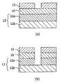
Translated fromKorean도 1은 본 발명의 패턴 형성 방법에 관한 설명도로서, (a)는 현상 후의 레지스트 패턴, (b)는 기판의 건식 에칭 후의 패턴을 나타낸다.1: is explanatory drawing about the pattern formation method of this invention, (a) shows the resist pattern after image development, (b) shows the pattern after dry etching of a board | substrate.
도 2는 본 발명의 다른 패턴 형성 방법에 관한 설명도로서, (a)는 현상 후의 레지스트 패턴, (b)는 반사 방지막에 전사된 패턴, (c)는 유기막에 전사된 패턴, (d)는 기판의 건식 에칭 후의 패턴을 나타낸다.2 is an explanatory diagram of another pattern forming method of the present invention, (a) is a resist pattern after development, (b) is a pattern transferred to an antireflection film, (c) is a pattern transferred to an organic film, and (d) Represents the pattern after the dry etching of the substrate.
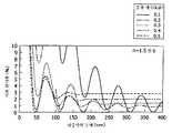
도 3은 반사 방지막의 막 두께와 반사율의 관계를 나타내는 그래프로서, 다양한 k값 대한 기판 반사율을 나타낸다.3 is a graph showing the relationship between the film thickness and the reflectance of the antireflection film, and shows the substrate reflectance for various k values.
<도면의 주요 부분에 대한 부호의 설명><Explanation of symbols for the main parts of the drawings>
10, 20: 반사 방지막10, 20: antireflection film
11, 21: 포토레지스트 막11, 21: photoresist film
12, 22: 기판12, 22: substrate
12a, 22a: 피가공층12a, 22a: layer to be processed
12b, 22b: 바탕층12b, 22b: base layer
23: 유기 막23: organic membrane
본 발명은 반도체 소자 등의 제조 공정에서의 미세 가공에 사용되는 반사 방지막 재료로서 바람직한, 규소 원자를 함유하는 치환기를 함유하는 화합물을 주성분으로 하는 반사 방지막 재료 및 이것을 이용한 원자외선, ArF 엑시머 레이저광(193 nm), F2 레이저광(157 nm), Kr2레이저광(146 nm), Ar2레이저광(126 nm) 등의 노광에 바람직한 레지스트 패턴 형성 방법 및 기판에의 집적 회로 패턴 형성 방법에 관한 것이다.INDUSTRIAL APPLICABILITY The present invention relates to an antireflection film material containing a compound containing a substituent containing silicon atoms as a main component, which is preferable as an antireflection film material used for microfabrication in manufacturing processes such as semiconductor devices, and far ultraviolet rays using the same, and an ArF excimer laser light ( 193 nm), F2 laser light (157 nm), Kr2 laser light (146 nm), Ar2 laser light (126 nm) and the like, a resist pattern forming method suitable for exposure and an integrated circuit pattern forming method on a substrate will be.
최근 LSI의 고집적화와 고속도화에 따른 패턴 룰의 미세화가 요망되고 있는 가운데, 현재 범용 기술로서 이용되고 있는 광 노광을 이용한 리소그래피에 있어서는 광원의 파장에서 유래하는 본질적인 해상도의 한계에 근접하고 있다.In recent years, finer pattern rules have been demanded due to higher integration and higher speed of LSI, and in lithography using light exposure, which is currently used as a general-purpose technology, it is approaching the limit of intrinsic resolution derived from the wavelength of the light source.
레지스트 패턴 형성시에 사용되는 리소그래피용 광원으로서, 수은등의 g 선(436 nm) 또는 i 선(365 nm)을 광원으로 하는 광 노광이 널리 사용되고, 한층 더 미세화를 위한 수단으로서 노광 광을 단파장화하는 방법이 유효하게 이용되어 왔다. 이 때문에, 64 M 비트 DRAM 가공 방법의 양산 공정에는, 노광 광원으로서 i 선(365 nm) 대신에 단파장의 KrF 엑시머 레이저(248 nm)가 이용되었다. 그러나, 더욱 미세한 가공 기술(가공 치수가 0.13 ㎛ 이하)을 필요로 하는 집적도 1 G 이상의 DRAM 제조에는 보다 단파장의 광원이 필요하고, 특히 ArF 엑시머 레이저(193 nm)를 이용한 리소그래피가 검토되고 있다.As a lithography light source used in forming a resist pattern, light exposure using a g line (436 nm) or an i line (365 nm) as a light source is widely used, and shortening the exposure light as a means for further miniaturization. The method has been used effectively. For this reason, instead of the i line (365 nm), a short wavelength KrF excimer laser (248 nm) was used for the mass production process of the 64 M-bit DRAM processing method. However, in the manufacture of DRAMs with an integration degree of 1 G or more requiring finer processing techniques (processing dimensions of 0.13 µm or less), a shorter light source is required, and in particular, lithography using an ArF excimer laser (193 nm) has been studied.
KrF 리소그래피의 초기 단계에 있어서 색지움 렌즈 또는 반사 광학계 등과, 브로드 밴드(broad band) 광을 조합한 스테퍼가 개발되었다. 그러나, 색지움 렌즈 또는 비구면(非球面) 반사 광학계의 정밀도가 충분하기 않았기 때문에, 협대역(挾帶域)화된 레이저광과 굴절 광학계 렌즈의 조합이 주류가 되었다. 일반적으로, 단일 파장 노광에 있어서는 입사하는 광과 기판으로부터의 반사광이 간섭하여 정재파를 발생하는 것은, 이전부터 잘 알려져 있던 현상이다. 또한, 기판의 요철에 의해 빛이 집광 또는 산란되는 것에 의한 헐레이션이라 불리는 현상이 일어나는 것도 알려져 있다. 정재파와 헐레이션은 모두 패턴의 선폭 등의 치수 변동이나 형상의 붕괴 등을 야기한다. 간섭성인 단색광의 사용은 단파장화와 동시에 정재파나 헐레이션을 더욱 증폭시킨다. 이 때문에 헐레이션이나 정재파를 억제하는 방법으로서, 포토레지스트에 흡광제를 넣는 방법, 레지스트 상면 및 기판면에 반사 방지막을 두는 방법이 제안되었다. 그러나, 흡광제를 넣는 방법은 레지스트 패턴 형상이 테이퍼 형상이 되는 문제를 일으켰다. 최근 파장의 단파장화와 미세화의 진행과 동시에, 정재파와 헐레이션이 패턴 치수 변동에 미치는 문제가 심각하게 되어, 흡광제를 넣는 방법으로서는 충분히 대응할 수 없게 되었다.In the early stages of KrF lithography, steppers have been developed that combine broadband lenses, such as chromate lenses or reflective optics. However, since the precision of the chromium lens or the aspherical reflective optical system was not sufficient, the combination of the narrow band laser light and the refractive optical lens became the mainstream. In general, in a single wavelength exposure, it is a phenomenon that has been well known for a long time that incident light and reflected light from a substrate interfere with each other to generate standing waves. It is also known that a phenomenon called halation caused by condensation or scattering of light due to irregularities of the substrate occurs. Both standing waves and halation cause dimensional fluctuations such as the line width of the pattern, collapse of the shape, and the like. The use of coherent monochromatic light further amplifies standing waves and halation at the same time as shortening wavelengths. For this reason, as a method of suppressing halation and standing waves, a method of placing a light absorber in a photoresist and a method of providing an antireflection film on the upper surface of the resist and the substrate surface have been proposed. However, the method of adding a light absorber has caused a problem that the resist pattern shape becomes a tapered shape. In recent years, with the progress of shortening and miniaturization of wavelengths, problems of standing waves and halation on pattern dimensional fluctuations become serious, and as a method of adding a light absorber, it cannot be sufficiently coped with.
상층 투과형 반사 방지막은 원리적으로 정재파의 저감에만 효과가 있고, 헐레이션에는 효과가 없다. 또한, 정재파를 완전히 소멸시키기 위한 상층 투과형 반사 방지막의 굴절률은, 레지스트의 굴절률의 평방근이 이상적이기 때문에, KrF에서 사용되고 있는 폴리히드록시스티렌계 레지스트의 굴절률 1.8에서는, 1.34가 이상치 이다. ArF에 사용되고 있는 지환족계 아크릴 레지스트의 굴절률 1.6에서는, 이상치가 1.27이 된다. 이러한 낮은 굴절률을 갖는 재료는 퍼플루오로계 재료로 한정되지만, 상층 반사 방지막은 알칼리 현상시에 박리가 가능한 것이 공정적으로 유리하기 때문에, 수용성 재료인 것이 필요하다. 매우 소수성이 높은 퍼플루오로계 재료를 수용성으로 만들기 위해서, 친수성 치환기를 도입하면 굴절률이 증가하고, KrF에서는 1.42 전후, ArF에 있어서는 1.5 전후의 값이 된다. 이 때문에 KrF 리소그래피에서 0.20 ㎛ 이하의 패턴화를 행하는 경우에는, 흡광제와 상층 반사 방지막의 조합만으로는 정재파의 영향을 억제할 수 없었다. ArF에 있어서는, 상기 이유로 인해 상층 반사 방지막의 효과는 거의 기대할 수 없고, KrF에 있어서도 금후 한층 더 선폭이 축소됨으로써 선폭의 관리가 엄격해지자, 레지스트의 바탕에 반사 방지막을 두는 것이 필요해졌다.The upper transmissive antireflection film is effective only in reducing standing waves in principle, and has no effect in halation. In addition, since the square root of the refractive index of a resist is ideal for the refractive index of the upper permeation | transmission antireflection film in order to completely eliminate a standing wave, 1.34 is an ideal value in the refractive index 1.8 of the polyhydroxy styrene resist used by KrF. At refractive index 1.6 of the alicyclic acrylic resist used for ArF, the outlier becomes 1.27. The material having such a low refractive index is limited to a perfluoro-based material. However, the upper anti-reflection film is required to be a water-soluble material because it is advantageous to be able to peel off during alkali development. In order to make a very hydrophobic perfluoro-based material water-soluble, the introduction of a hydrophilic substituent increases the refractive index, and the value is around 1.42 in KrF and about 1.5 in ArF. For this reason, when patterning 0.20 micrometer or less in KrF lithography, only the combination of a light absorber and an upper anti-reflective film could not suppress the influence of a standing wave. In ArF, the effect of the upper antireflection film can hardly be expected due to the above reason, and in KrF, the line width is further reduced in the future, so that the management of the line width becomes strict, and it is necessary to provide an antireflection film on the resist base.
레지스트의 바탕인 반사 방지막은, 그의 아래가 폴리실리콘이나 알루미늄 등의 고반사 기판인 경우에는, 최적의 굴절률(n값), 흡광 계수(k값)의 재료를 적절한 막 두께로 설정함으로써 기판으로부터의 반사를 1 % 이하로 저감할 수 있어, 매우 큰 효과를 발휘할 수 있다. 예를 들면 파장 193 nm에서 레지스트의 굴절률이 1.8일 때, 하층 반사 방지막의 굴절률(굴절률의 실수부) n=1.5, 소광 계수(굴절률의 허수부) k=0.5, 막 두께 42 nm이면, 반사율이 0.5 % 이하가 된다(도 3 참조). 그러나, 바탕에 단차가 있는 경우에는, 단차상에서 반사 방지막의 막 두께가 크게 변동한다. 바탕의 반사 방지 효과는 빛의 흡수 뿐만 아니라, 간섭 효과도 이용하고 있기 때문에, 간섭 효과가 강한 막 두께 40 내지 45 nm의 제1 저변은 그 만큼 반사 방지 효과도 높지만, 막 두께의 변동에 의해 반사율이 크게 변동한다. 반사 방지막 재료에 사용되는 기재 수지의 분자량을 높여 단차상에서의 막 두께 변동을 억제하고 순응성(conformal)을 높인 재료가 제안되어 있지만(예를 들면, 일본 특허 공개 (평) 10-69072호 공보 참조), 기재 수지의 분자량이 커지면, 스핀 코팅 후에 핀 홀이 발생하기 쉬워진다는 문제나, 여과할 수 없어진다는 문제, 경시적으로 점도 변동이 생겨 막 두께가 변화한다는 문제나, 노즐 선단에 결정물이 석출한다는 문제가 발생하고, 또한 순응성을 발휘할 수 있는 것은 비교적 높이가 낮은 단차로 한정된다.The antireflection film, which is the base of the resist, is formed from a high reflection substrate such as polysilicon or aluminum, and is formed from an appropriate film thickness by setting a material having an optimum refractive index (n value) and an extinction coefficient (k value) to an appropriate film thickness. The reflection can be reduced to 1% or less, and a very large effect can be exhibited. For example, when the refractive index of the resist is 1.8 at a wavelength of 193 nm, if the refractive index (the real part of the refractive index) n = 1.5, the extinction coefficient (the imaginary part of the refractive index) k = 0.5, and the film thickness of the lower layer antireflection film, the reflectance is It becomes 0.5% or less (refer FIG. 3). However, when there is a step on the ground, the film thickness of the anti-reflection film fluctuates greatly on the step. Since the anti-reflective effect of the background uses not only light absorption but also interference effects, the first base of the film thickness of 40 to 45 nm, which has a strong interference effect, has a high anti-reflection effect, but the reflectance is caused by the variation of the film thickness. This fluctuates greatly. A material is proposed in which the molecular weight of the base resin used in the antireflection film material is increased to suppress the film thickness variation in the stepped phase and increase the conformality (see, for example, Japanese Patent Application Laid-Open No. Hei 10-69072). When the molecular weight of the base resin increases, problems such as pin holes tend to occur after spin coating, filtration cannot be obtained, viscosity fluctuates over time, and film thickness changes, and crystals at the tip of the nozzle The problem of precipitation occurs, and the ability to exhibit compliance is limited to a step with a relatively low height.
다음으로, 막 두께 변동에 의한 반사율의 변동이 비교적 작은 제3 저변 이상의 막 두께(170 nm 이상)를 채용하는 방법을 생각할 수 있다. 이 경우, k값이 0.2 내지 0.3의 사이이고, 막 두께가 170 nm 이상이면 막 두께의 변화에 대한 반사율의 변동이 작고, 더구나 반사율을 1.5 % 이하로 억제할 수 있게 된다. 반사 방지막의 바탕이 산화막이나 질화막 등의 투명막이고, 이 투명막 아래에 단차가 있는 경우, 투명막의 표면이 CMP 등으로 평탄화되어 있다고 해도, 투명막의 막 두께가 변동한다. 이 경우, 그 위의 반사 방지막의 막 두께를 일정하게 하는 것은 가능하지만, 반사 방지막의 바탕 투명막의 막 두께가 변동하면, 도 3에서의 최저 반사율이 되는 막의 두께가 투명막의 막 두께분만큼 λ/2n(λ: 노광 파장, n: 노광 파장에서의 투명막의 굴절률)의 주기로 어긋나게 된다. 반사 방지막의 막 두께를, 바탕이 반사막일 때의 최저 반사율이 되는 막 두께 55 nm로 설정한 경우, 투명막의 막 두께 변동에 의해서 반사율이 높은 부분이 출현한다. 이 경우, 바탕 투명막의 막 두 께의 변화에 대한 반사율을 안정화하기 위해서도, 상술한 바와 같은 반사 방지막의 막 두께가 170 nm 이상인 막으로 만들 필요가 있다.Next, a method of employing a film thickness (170 nm or more) of a third base or more that is relatively small in fluctuation in reflectance due to film thickness fluctuation can be considered. In this case, when the k value is between 0.2 and 0.3, and the film thickness is 170 nm or more, the variation in reflectance with respect to the change in film thickness is small, and the reflectance can be suppressed to 1.5% or less. If the base of the antireflection film is a transparent film such as an oxide film or a nitride film, and there is a step below the transparent film, even if the surface of the transparent film is flattened with CMP or the like, the film thickness of the transparent film fluctuates. In this case, it is possible to make the film thickness of the antireflective film thereon constant, but when the film thickness of the underlying transparent film of the antireflective film varies, the film thickness which becomes the lowest reflectance in FIG. 3 is λ / for the film thickness of the transparent film. It shifts in the period of 2n ((lambda): exposure wavelength, n: refractive index of a transparent film in an exposure wavelength). When the film thickness of the antireflection film is set to a film thickness of 55 nm, which is the minimum reflectance when the base is a reflecting film, a portion having a high reflectance appears due to the film thickness variation of the transparent film. In this case, in order to stabilize the reflectance with respect to the change in the film thickness of the base transparent film, it is necessary to make the film having the above-described antireflection film thickness of 170 nm or more.
반사 방지막의 재료는 무기계와 유기계로 크게 구별할 수 있다. 무기계는 SiON막을 들 수 있다. 이것은 실란과 암모니아의 혼합 가스에 의한 CVD 등으로 형성되고, 레지스트에 대한 에칭 선택비가 크기 때문에, 레지스트에의 에칭의 부하가 작은 이점이 있지만 박리가 곤란하기 때문에, 적용할 수 있는 경우에 제한이 있다.The material of the antireflection film can be broadly classified into inorganic and organic. An inorganic type is a SiON film. This is formed by CVD with a mixed gas of silane and ammonia, and has a large etching selectivity to the resist, so that the etching load on the resist is small, but since peeling is difficult, there is a limitation in the case where it can be applied. .
질소 원자를 포함하는 염기성 기판이기 때문에, 포지티브형 레지스트에서는 풋팅(footing), 네가티브형 레지스트에서는 언더컷트 프로파일이 되기 쉽다는 결점도 있다. 유기계는 스핀 코팅이 가능하고 CVD나 스퍼터링 등의 특별한 장치를 필요로 하지 않는 점, 레지스트와 동시에 박리 가능한 점, 해밍 등의 발생이 없이 형상이 순수하고 레지스트와의 접착성도 양호한 점이 이점이어서, 많은 유기 재료를 기재로 한 반사 방지막 재료가 제안되었다. 예를 들면, 일본 특허 공고 (평)7-69611호 공보에 기재된 디페닐아민 유도체와 포름알데히드 변성 멜라민 수지와의 축합체, 알칼리 가용성 수지와 흡광제로 이루어지는 것이나, 미국 특허 제5294680호에 기재된 말레산 무수물 공중합체와 디아민형 흡광제의 반응물, 일본 특허 공개 (평)6-118631호 공보에 기재된 수지 결합제와 메틸올멜라민계 열가교제를 함유하는 것, 일본 특허 공개 (평)6-118656호 공보에 기재된 카르복실산기와 에폭시기와 흡광기를 동일한 분자 내에 갖는 아크릴 수지 기재형, 일본 특허 공개 (평)8-87115호 공보에 기재된 메틸올멜라민과 벤조페논계 흡광제로 이루어지는 것, 일본 특허 공개 (평)8-179509호 공보에 기재된 폴리비닐알코올 수지에 저분자 흡광제를 첨가한 것 등을 들 수 있다. 이들은 모두 결합제 중합체에 흡광제를 첨가하거나, 또는 중합체에 치환기로서 도입하는 방법을 채용하고 있다. 그러나, 흡광제의 대부분이 방향족기 또는 2중 결합을 갖기 때문에, 흡광제의 첨가에 의해 건식 에칭 내성이 높아지고, 포토레지스트와의 건식 에칭 선택비가 그만큼 높지 않다는 결점이 있다. 미세화가 진행되고, 포토레지스트의 박막화에도 박차가 가해지고 있으며, 차세대의 ArF 노광에 있어서는 레지스트 재료에 아크릴 또는 지환족 중합체를 사용하기 때문에, 레지스트의 에칭 내성이 저하된다. 또한, 상술한 바와 같이, 반사 방지막의 막 두께를 두껍게 해야만 한다는 문제도 있다. 이 때문에, 에칭은 심각한 문제이고, 레지스트에 대하여 에칭 선택비가 높은, 즉 에칭 속도가 빠른 반사 방지막이 요구되고 있다.Since it is a basic substrate containing a nitrogen atom, there also exists a drawback that it becomes easy to become a footing in a positive type resist and an undercut profile in a negative type resist. The organic system is advantageous in that spin coating is possible and does not require a special device such as CVD or sputtering, it can be peeled off at the same time with the resist, and the shape is pure without the occurrence of hamming, and the adhesion with the resist is good. An antireflection film material based on the material has been proposed. For example, the condensate of the diphenylamine derivative described in JP-A-7-69611 and formaldehyde-modified melamine resin, an alkali-soluble resin and a light absorber, or maleic acid described in US Pat. No. 5294680. A reaction product of an anhydride copolymer and a diamine light absorber, containing a resin binder as described in JP-A-6-118631 and a methylolmelamine-based thermal crosslinking agent, JP-A-6-118656 Acrylic resin base type which has a carboxylic acid group, an epoxy group, and a light absorber in the same molecule, What consists of methylol melamine and a benzophenone type light absorber as described in Unexamined-Japanese-Patent No. 8-87115, Unexamined-Japanese-Patent No. 8 The addition of the low molecular weight absorber to the polyvinyl alcohol resin of -179509 is mentioned. All of these employ | adopt the method which adds a light absorber to a binder polymer, or introduce | transduces into a polymer as a substituent. However, since most of the light absorbers have aromatic groups or double bonds, there is a drawback that the dry etching resistance is increased by the addition of the light absorbing agent, and the dry etching selectivity with the photoresist is not so high. Miniaturization progresses, spurs are also applied to the thinning of the photoresist, and in the next generation of ArF exposure, since the acrylic or alicyclic polymer is used as the resist material, the etching resistance of the resist is reduced. Moreover, as mentioned above, there also exists a problem that the film thickness of an anti-reflective film must be made thick. For this reason, etching is a serious problem, and there is a need for an antireflection film having a high etching selectivity relative to the resist, that is, a high etching rate.
반사 방지막에 있어서 최적의 흡광 계수를 제공하기 위한 흡광제가 검토되고 있다. KrF에서는 특히 안트라센형, ArF에서는 페닐형이 제안되어 있다. 그러나, 이들은 상술한 바와 같이 우수한 건식 에칭 내성을 갖는 치환기이기도 하고, 다이를 펜던트시킨 중합체 골격을 아크릴 등의 에칭 내성이 낮은 중합체로 만든 경우에 있어서도 실용적으로는 한계가 있다. 한편, 일반적으로 규소를 포함하는 재료는 플루오로카본계 가스를 이용한 에칭 조건에서 에칭 속도가 빠르고, 레지스트에 대하여 높은 선택비가 얻어지는 것으로 알려져 있고, 규소 원자를 포함하는 반사 방지막을 이용함으로써 에칭의 선택비를 비약적으로 높일 수 있다고 생각된다. 예를 들면, 페닐기가 펜던트된 폴리실란을 골격으로 하는 KrF 노광용의 반사 방지막이 일본 특허 공개 (평)11-60735호 공보에 제안되어, 높은 에칭 선택비가 달성되었다.A light absorber for providing an optimal extinction coefficient in an antireflection film has been studied. Especially in KrF, anthracene type and a phenyl type in ArF are proposed. However, these are also substituents having excellent dry etching resistance as described above, and there is a practical limitation even when the polymer skeleton in which the die is pendant is made of a polymer having low etching resistance such as acrylic. On the other hand, in general, a material containing silicon is known to have a high etching rate under etching conditions using a fluorocarbon-based gas, and a high selectivity to the resist can be obtained, and the selectivity of etching can be obtained by using an antireflection film containing silicon atoms. I think it can increase dramatically. For example, an anti-reflective film for KrF exposure having a polysilane having a phenyl group pendant thereon is proposed in Japanese Patent Laid-Open No. 11-60735, and a high etching selectivity is achieved.
최근 고해상도화에 따라 레지스트 막의 박막화가 진행되고 있다. 박막화에 따라 레지스트의 에칭 내성 향상이 요구되고 있지만, 충분하지 않다. 박막 레지스트의 패턴 전사 방법으로서 하드 마스크법이 있다. 피가공 기판이 p-Si 등에서는 SiO2막, 피가공 기판이 SiO2막에서는 SiN, W-Si, 비정질 Si 등이 검토되고 있다. 하드 마스크를 남기는 경우와 박리하는 경우가 있지만, 특히 바탕이 SiO2막 등의 절연막인 경우, 특히 W-Si, 비정질 Si막은 양호한 도전성 막이기 때문에 박리하는 것이 필요하다. SiN막은 절연막이기 때문에, 경우에 따라서는 박리할 필요가 없지만, SiO2와 구성 원소가 유사하기 때문에, 하드 마스크의 원래 기능으로서의 에칭 선택비가 낮다는 결점이 있다. 또한, 반사 방지막으로서의 기능을 겸한 SiON막의 하드 마스크가 제안되어 있다(예를 들면, 문헌[SPIE 2000, Vol. 4226 p93] 참조).In recent years, the thinning of a resist film is progressing with high resolution. Although it is required to improve the etching resistance of the resist with thinning, it is not enough. There is a hard mask method as a pattern transfer method of a thin film resist. Etc. The p-Si substrate to be processed is in the SiO2 film, a processed substrate is a SiO2 film such as SiN, W-Si, amorphous Si has been studied. Although a hard mask may be left and it may be peeled off, especially when the base is an insulating film such as a SiO2 film, in particular, since the W-Si and amorphous Si film are good conductive films, it is necessary to peel off. Since the SiN film is an insulating film, there is no need to peel in some cases, but since SiO2 and the constituent elements are similar, there is a drawback that the etching selectivity as an original function of the hard mask is low. In addition, a hard mask of a SiON film that also serves as an antireflection film has been proposed (see, for example, SPIE 2000, Vol. 4226 p93).
여기서, 일본 특허 공개 (소)57-83563호 공보, 일본 특허 공개 (평)57-131250호 공보, 일본 특허 공개 (소)56-129261호 공보, 일본 특허 제3287119호 공보, 일본 특허 공개 2001-22082호 공보, 일본 특허 공개 2001-22083호 공보에 실리카계 절연막 형성용 도포액이 제안되어 있다. 이 기술을 이용하여, 레지스트의 하층막으로서 규소 함유 중합체를 사용하는 많은 패턴 형성 방법이 제안되어 있다. 예를 들면, 일본 특허 제3118887호 공보, 일본 특허 공개 2000-356854호 공보에는 기판 상에 유기막을 형성하고, 그 위에 실리카 유리를 스핀 코팅하며, 그 위의 레지스트 패턴을 실리카 유리층에 전사하고, 다음으로 산소 가스 에칭으로 유기막층에 패턴 전사하고, 마지막으로 기판을 가공하는 3층 공정이 제안되어 있다. 일본 특허 공개 (평)5-27444호 공보, 일본 특허 공개 (평)6-138664호 공보, 일본 특허 공개 2001-53068호 공보, 일본 특허 공개 2001-92122호 공보, 일본 특허 공개 2001-343752호 공보에는, 반사 방지막으로서의 효과도 겸한 실리카 유리층, 실세스퀴옥산 중합체 재료가 제안되어 있다. 또한, 미국 특허 제6420088호에는 실세스퀴옥산 중합체를, 일본 특허 공표 2003-502449호에는 스핀 온 글래스 재료를 기재로 한 반사 방지막과 하드 마스크의 기능을 겸비한 재료가 제안되어 있다. 그러나, 모든 규소 함유 중합체는 보존 안정성에 문제가 있어, 실제 사용시에 막 두께가 변동한다는 치명적인 결함이 존재하였다.Here, Japanese Patent Laid-Open No. 57-83563, Japanese Patent Laid-Open No. 57-131250, Japanese Patent Laid-Open No. 56-129261, Japanese Patent No. 3287119, and Japanese Patent Laid-Open 2001- A coating liquid for forming a silica-based insulating film is proposed in Japanese Patent Laid-Open No. 22082 and Japanese Patent Laid-Open No. 2001-22083. Using this technique, many pattern formation methods using the silicon containing polymer as an underlayer film of a resist are proposed. For example, Japanese Patent No. 3118887 and Japanese Patent Laid-Open No. 2000-356854 disclose that an organic film is formed on a substrate, spin-coated silica glass thereon, and the resist pattern thereon is transferred to a silica glass layer, Next, the three-layer process of carrying out the pattern transfer to the organic film layer by oxygen gas etching, and finally processing a board | substrate is proposed. Japanese Patent Laid-Open No. 5-27444, Japanese Patent Laid-Open No. 6-138664, Japanese Patent Laid-Open No. 2001-53068, Japanese Patent Laid-Open No. 2001-92122, Japanese Patent Laid-Open No. 2001-343752 The silica glass layer and silsesquioxane polymer material which also serve as an antireflection film are proposed to the following. In addition, U.S. Patent No. 6420088 proposes a silsesquioxane polymer, and Japanese Patent Publication No. 2003-502449 proposes a material that combines the functions of an antireflection film and a hard mask based on a spin on glass material. However, all silicon-containing polymers have a problem in storage stability, and a fatal defect exists that the film thickness fluctuates in actual use.
본 발명이 해결하려고자 하는 과제는 레지스트에 대하여 에칭 선택비가 높고, 즉 레지스트에 대하여 에칭 속도가 빠르며 장기 보존에도 막 두께 변동이 적은 반사 방지막의 재료를 제공하고, 이 반사 방지막 재료를 이용하여 기판 상에 반사 방지막층을 형성하는 패턴 형성 방법, 및 상기 반사 방지막을 기판 가공의 하드 마스크로서 이용하는 패턴 형성 방법도 제공하는 것이다.The problem to be solved by the present invention is to provide a material of an antireflection film having a high etching selectivity with respect to the resist, that is, a high etching rate with respect to the resist and a small variation in film thickness even in long-term storage, and using the antireflection film material on the substrate It also provides a pattern forming method for forming an antireflection film layer on the substrate, and a pattern forming method using the antireflection film as a hard mask for substrate processing.
반사 방지막에 요구되는 성능의 하나로서, 레지스트와의 인터믹싱이 없는 것, 레지스트층에의 저분자 성분의 확산이 없는 것을 들 수 있다(Proc. SPIE Vol.2195, 225-229(1994)). 이들을 방지하기 위해서, 일반적으로 반사 방지막의 스핀 코팅 후 베이킹하여 열 가교한다는 방법이 채용되고 있다. 또한, 반사 방지막 또는 레지스트 하층막 상의 레지스트 패턴은 해밍 또는 언더컷트가 없는 수직 형상인 것이 요구된다. 해밍 형상에서는 반사 방지막의 에칭 후에 치수 변환차가 생기고, 언더컷트 형상에서는 현상 후에 레지스트 패턴의 붕괴가 일어나기 때문이다.As one of the performances required for the antireflection film, there is no intermixing with the resist and no diffusion of low molecular weight components into the resist layer (Proc. SPIE Vol. 2195, 225-229 (1994)). In order to prevent these, the method of baking and thermally crosslinking after the spin coating of an antireflection film is employ | adopted generally. In addition, the resist pattern on the antireflection film or the resist underlayer film is required to have a vertical shape without hamming or undercut. This is because a dimensional conversion difference occurs after etching of the antireflection film in the hamming shape, and collapse of the resist pattern occurs after development in the undercut shape.
문헌[Proc. SPIE Vol.3678, 241-250(1999)]에는, 산에 의한 가교는 포지티브형 레지스트의 해밍 저감에 유효한 것으로 보고되어 있다. 가교제를 첨가하고, 산에 의해 가교시키는 방법은 반사 방지막 재료에 있어서 중요하고, 상기 일본 특허 공개 2001-92122호 공보 및 일본 특허 공개 (평)5-27444호 공보에서는 가교제의 첨가가 유효하다고 되어 있다.Proc. SPIE Vol. 3678, 241-250 (1999) reports that acid crosslinking is effective for reducing the hamming of positive resists. The method of adding a crosslinking agent and crosslinking with an acid is important for the antireflection film material, and the addition of the crosslinking agent is effective in Japanese Patent Laid-Open Nos. 2001-92122 and JP-A-5-27444. .
여기서, 현상 후의 포토레지스트의 단면 패턴이 역테이퍼 형상이 되는 문제가 발생하고 있다. 이것은 반사 방지막의 가교 반응에 사용되는 산이 레지스트층으로 이동하여, 베이킹시에 레지스트의 산불안정기를 이탈시키거나, 또는 레지스트 중에 첨가된 아민 화합물을 중화시킨 것이 원인이라고 생각된다. 레지스트층에 산이 이동하지 않도록 하기 위해서는, 반사 방지막에 발생하는 산을 벌키(bulky)한 것으로 만드는 방법을 들 수 있지만, 가교 반응도 진행하기 어려워지고, 레지스트와의 인터믹싱의 원인이 되기 때문에 바람직하지 않다. 여기서, 문헌[SPIE Vol.3678, p702(1999)]에는 ArF용 유기 반사 방지막으로서, 히드록시에틸메타크릴레이트, 메틸아크릴레이트, 스티렌의 3원 공중합체를 사용한 재료가 제안되어 있다. 가교 시스템으로서는 히드록시에틸메타크릴레이트와 글리콜우릴계의 가교제를 사용하고 있다. 여기서 주목하고자 하는 것은 메틸아크릴레이트의 존재이고, 이것을 공중합함으로써 역테이퍼를 방지하고 있다. 메틸아크릴레이트는 레지스트와의 밀착성을 향상시키고, 산 확산을 억제하는 효과도 있다고 생각된다. 역테이퍼 형상 방지를 위해서는, 가교 후의 반사 방지막 중에 산을 밀폐시켜 둘 필요가 있고, 이를 위해서는 카르보닐, 에스테르, 락톤, 에테르기 등의 탄소-산소 단일 결합 및(또는) 이중 결합을 함유하는 유기기를 갖는 중합체를 사용하는 것이 유효하고, 상기 관능기를 펜던트한 실록산 중합체 수지를 반사 방지막으로서 사용하는 것을 고안하였다.Here, there arises a problem that the cross-sectional pattern of the photoresist after development becomes an inverse taper shape. This is considered to be caused by the acid used for the crosslinking reaction of the antireflection film moving to the resist layer, leaving the acid labile group of the resist during baking, or neutralizing the amine compound added in the resist. In order to prevent the acid from moving in the resist layer, a method of making the acid generated in the anti-reflection film bulky is mentioned. However, the crosslinking reaction also becomes difficult to proceed and causes intermixing with the resist, which is not preferable. . Here, SPIE Vol. 3678, p702 (1999) proposes a material using ternary copolymers of hydroxyethyl methacrylate, methyl acrylate and styrene as an organic antireflection film for ArF. As a crosslinking system, a hydroxyethyl methacrylate and a glycoluril crosslinking agent are used. Attention here is the presence of methyl acrylate, and the reverse taper is prevented by copolymerizing it. It is thought that methyl acrylate also has the effect of improving the adhesiveness with a resist and suppressing acid diffusion. In order to prevent the reverse taper shape, it is necessary to seal the acid in the antireflection film after crosslinking. For this purpose, an organic group containing carbon-oxygen single bonds and / or double bonds such as carbonyl, ester, lactone, and ether groups is required. It is effective to use the polymer which has, and devised to use the siloxane polymer resin which penetrated the said functional group as an antireflection film.
또한, 본 발명에서는 가교 반응 기작을 예의 연구한 결과, 중합체 중에 잔존하고 있는 실라놀기가 가교 반응에 크게 기여하고 있어, 종래 필수이었던 가교제를 첨가하지 않아도, 임의의 특정한 양의 실라놀기가 존재하면 실질상 문제가 없는 반사 방지막을 얻을 수 있음을 발견하였다.Further, in the present invention, as a result of intensive study of the crosslinking reaction mechanism, the silanol groups remaining in the polymer greatly contribute to the crosslinking reaction, and if any specific amount of silanol groups is present It was found that an antireflection film without a phase problem can be obtained.
즉, 본 발명은 탄소-산소 단일 결합 및(또는) 탄소-산소 이중 결합을 갖는 유기기와, 광 흡수기와, 말단이 Si-OH 및(또는) Si-OR로 되어 있는 규소 원자를 포함하여 이루어지는 반사 방지용 실리콘 수지를 제공한다. 또한, 상기 (A) 반사 방지막용 실리콘 수지, (B) 유기 용제 및 (C) 산 발생제를 함유하는 반사 방지막 재료를 제공한다.That is, the present invention is a reflection comprising an organic group having a carbon-oxygen single bond and / or a carbon-oxygen double bond, a light absorber, and a silicon atom whose terminal is Si-OH and / or Si-OR. It provides a prevention silicone resin. Moreover, the antireflection film material containing the said (A) silicone resin for antireflection film, (B) organic solvent, and (C) acid generator is provided.
또한, 본 발명은 리소그래피에 의해 기판에 패턴을 형성하는 방법으로서, 적어도 기판 상에 반사 방지막 재료를 도포하고 베이킹하여 반사 방지막을 형성하고, 이 반사 방지막 상에 포토레지스트 막 재료를 도포하고 예비베이킹하여 포토레지스트 막을 형성하며, 이 포토레지스트 막의 패턴 회로 영역을 노광한 후, 현상액으로 현상하여 포토레지스트 막에 레지스트 패턴을 형성하고, 이 레지스트 패턴이 형성 된 포토레지스트 막을 마스크로 하여 반사 방지막 및 기판을 에칭하여 기판에 패턴을 형성하는 것을 포함하여 이루어지는 패턴 형성 방법을 제공한다.In addition, the present invention is a method of forming a pattern on a substrate by lithography, at least by applying and baking an antireflection film material on the substrate to form an antireflection film, by applying a photoresist film material on the antireflection film and prebaking After forming a photoresist film, exposing the pattern circuit area of the photoresist film, developing it with a developer to form a resist pattern on the photoresist film, and etching the antireflection film and the substrate using the photoresist film on which the resist pattern is formed as a mask. To provide a pattern forming method comprising forming a pattern on a substrate.
본 발명의 리소그래피에 의한 기판에의 패턴 형성의 바람직한 양태로서, 적어도 기판 상에 반사 방지막 재료를 도포하고 베이킹하여 반사 방지막을 형성하고, 이 반사 방지막 상에 포토레지스트 막 재료를 도포하고 예비베이킹하여 포토레지스트 막을 형성하며, 이 포토레지스트 막의 패턴 회로 영역을 노광한 후, 현상액으로 현상하여 포토레지스트 막에 레지스트 패턴을 형성하고, 이 레지스트 패턴이 형성된 포토레지스트 막을 마스크로 하여 반사 방지막을 에칭하며, 또한 패턴이 형성된 반사 방지막을 마스크로 하여 기판을 에칭하고 기판에 패턴을 형성하는 것을 포함하여 이루어지는 패턴 형성 방법을 제공한다.As a preferred embodiment of the pattern formation on the substrate by lithography of the present invention, an antireflection film material is applied and baked on at least the substrate to form an antireflection film, and a photoresist film material is applied on the antireflection film and prebaked to provide a photo. A resist film is formed, the pattern circuit area of the photoresist film is exposed, and then developed with a developer to form a resist pattern on the photoresist film. The antireflection film is etched using the photoresist film on which the resist pattern is formed as a mask. Provided are a pattern forming method comprising etching a substrate using the formed antireflective film as a mask and forming a pattern on the substrate.
본 발명의 리소그래피에 의한 기판에의 패턴 형성의 다른 바람직한 양태로서, 적어도 기판 상에 유기 막을 형성하고, 이 유기 막 위에 반사 방지막 재료를 도포하고 베이킹하여 반사 방지막을 형성하고, 이 반사 방지막 상에 포토레지스트 막 재료를 도포하고 예비베이킹하여 포토레지스트 막을 형성하며, 이 포토레지스트 막의 패턴 회로 영역을 노광한 후, 현상액으로 현상하여 포토레지스트 막에 레지스트 패턴을 형성하고, 이 레지스트 패턴이 형성된 포토레지스트 막을 마스크로 하여 반사 방지막을 에칭하며, 패턴이 형성된 반사 방지막을 마스크로 하여 유기 막을 에칭하고, 또한 기판을 에칭하고 기판에 패턴을 형성하는 것을 포함하는 패턴 형성 방법을 제공한다.As another preferred embodiment of pattern formation on a substrate by lithography of the present invention, an organic film is formed on at least the substrate, an antireflection film material is applied and baked on the organic film to form an antireflection film, and a photo on the antireflection film Applying a resist film material and prebaking to form a photoresist film, exposing the pattern circuit area of the photoresist film, developing with a developer to form a resist pattern on the photoresist film, and masking the photoresist film on which the resist pattern is formed. An antireflection film is etched, the organic film is etched using the antireflection film on which the pattern is formed as a mask, and the substrate is formed by etching the substrate and forming a pattern on the substrate.
또한, 노광은 바람직하게는 파장 300 nm 이하의 고에너지선 또는 전자선을 이용한다.In addition, exposure preferably uses high energy rays or electron beams having a wavelength of 300 nm or less.
또한, 본 발명의 반사 방지막 재료를 기판 상에 도포하고 베이킹하여 얻어지는 반사 방지막을 제공한다.The present invention also provides an antireflection film obtained by applying and baking the antireflection film material of the present invention on a substrate.
<발명의 실시 형태><Embodiment of the invention>
이하에, 본 발명에 대하여 더욱 상세하게 설명한다.EMBODIMENT OF THE INVENTION Below, this invention is demonstrated in detail.
본 발명에서 나타내는 실리콘 수지는, 바람직하게는 하기 화학식 1로 표시되는 규소 함유 화합물 1종 또는 2종 이상의 혼합물을 가수분해, 축합하여 얻을 수 있다.The silicone resin represented by this invention, Preferably, it can obtain by hydrolyzing and condensing the 1 type or 2 or more types of mixture containing the silicon represented by following formula (1).

식 중, R1a는 탄소-산소 단일 결합 및(또는) 탄소-산소 이중 결합을 갖는 유기기이고, R2는 광 흡수기를 갖는 1가의 유기기이고, X는 동일하거나 또는 상이한 할로겐 원자, 수소 원자, 히드록시기, 탄소수 1 내지 6의 알콕시기 또는 탄소수 1 내지 6의 알킬카르보닐옥시기이고, m과 n은 각각 0 내지 3의 정수로서, 0<(4-m-n)≤4의 관계를 만족시킨다.Wherein R1a is an organic group having a carbon-oxygen single bond and / or a carbon-oxygen double bond, R2 is a monovalent organic group having a light absorbing group, and X is the same or different halogen atom, hydrogen atom , A hydroxy group, an alkoxy group having 1 to 6 carbon atoms or an alkylcarbonyloxy group having 1 to 6 carbon atoms, and m and n each represent an integer of 0 to 3, satisfying a relationship of 0 <(4-mn) ≤4.
화학식 1로 표시되는 규소 함유 화합물의 바람직한 중량 평균 분자량은 GPC( 겔 투과 크로마토그래피)에 기초하는 측정에서 폴리스티렌 환산으로 500 내지 100만, 보다 바람직하게는 1000 내지 50만이다.The preferred weight average molecular weight of the silicon-containing compound represented by the formula (1) is 500 to 1 million, more preferably 1000 to 500,000 in terms of polystyrene in the measurement based on GPC (gel permeation chromatography).
본 발명의 탄소-산소 단일 결함 및(또는) 탄소-산소 이중 결합을 갖는 유기기는, 바람직하게는 탄소수 2 내지 30이고, 더욱 바람직하게는 에폭시기, 에스테르기, 알콕시기 및 히드록시기로부터 선택되는 1종 이상의 유기기이다. 유기기는 탄소를 포함하는 기를 의미하고, 수소, 질소, 황 등을 포함할 수도 있다. 본 발명의 탄소-산소 단일 결합 및(또는) 탄소-산소 이중 결합을 갖는 유기기는, 예로서 이하의 것을 들 수 있다.The organic group having a carbon-oxygen single defect and / or carbon-oxygen double bond of the present invention is preferably 2 to 30 carbon atoms, more preferably at least one selected from an epoxy group, an ester group, an alkoxy group and a hydroxy group. It is an organic group. The organic group means a group containing carbon, and may include hydrogen, nitrogen, sulfur, and the like. Examples of the organic group having a carbon-oxygen single bond and / or a carbon-oxygen double bond of the present invention include the following ones.
(P-Q1-(S1)v1-Q2-)u-(T)v2-Q3-(S2)v3-Q4-(PQ1- (S1 )v1 -Q2- )u- (T)v2 -Q3- (S2 )v3 -Q4-
식 중, P는 수소 원자, 히드록실기, 에폭시환(OCH2CH-), 탄소수 1 내지 4의 알콕시기, 탄소수 1 내지 6의 알킬카르보닐옥시기 또는 탄소수 1 내지 6의 알킬카르보닐기이고, Q1과 Q2와 Q3과 Q4는 각각 독립적으로 -CqH2q-pPp-(식 중, P는 상기와 동일하고, p는 0 내지 3의 정수이고, q는 0 내지 10의 정수임), u는 0 내지 3의 정수이고, S1과 S2는 각각 독립적으로 -O-, -CO-, -OCO-, -COO- 또는 OCOO을 나타낸다. v1, v2, v3은 각각 독립적으로 0 또는 1을 나타낸다. 이들과 함께, T의 예를 이하에 니타낸다. T에서 Q2와 Q3이 결합하는 위치는 특별히 한정되지 않지만, 입체적인 요인에 의한 반응성이나 반응에 사용되는 시판용 시약의 입수성 등을 고려하 여 적절하게 선택할 수 있다.In the formula, P is a hydrogen atom, a hydroxyl group, an epoxy ring (OCH2 CH-), an alkoxy group having 1 to 4 carbon atoms, an alkylcarbonyloxy group having 1 to 6 carbon atoms or an alkylcarbonyl group having 1 to 6 carbon atoms, Q1 , Q2 and Q3 and Q4 are each independently -Cq H2q-p Pp- (wherein P is the same as above, p is an integer of 0 to 3, q is 0 to 10 of U is an integer of 0 to 3, and S1 and S2 each independently represent —O—, —CO—, —OCO—, —COO—, or OCOO. v1, v2, and v3 each independently represent 0 or 1. With these, the example of T is shown below. The position at which Q2 and Q3 bind in T is not particularly limited, and may be appropriately selected in consideration of reactivity due to steric factors and availability of commercial reagents used for the reaction.

본 발명의 탄소-산소 단일 결합 및(또는) 탄소-산소 이중 결합을 갖는 유기기가 바람직한 예로서, 이하의 것을 들 수 있다. 또한, 화학식 중에서 (Si)는 Si와의 결합 부분을 나타내기 위하여 기재하였다.
The following are mentioned as a preferable example of the organic group which has a carbon-oxygen single bond and / or a carbon-oxygen double bond of this invention. In addition, in formula, (Si) was described in order to show the bonding part with Si.


다음으로, 본 발명의 광 흡수기는 파장 150 내지 300 nm의 범위에서 흡수를 갖는 기이고, 바람직하게는 안트라센환, 나프탈렌환, 벤젠환, 또는 이들 환에 1개 이상의 치환기를 갖는 것일 수도 있고, 치환기로서는 탄소수 1 내지 6의 알킬기, 탄소수 1 내지 6의 알콕시기, 탄소수 1 내지 6의 아실옥시 또는 탄소수 1 내지 6의 아세탈기가 바람직하고, 보다 바람직하게는 메틸기, 메톡시기, t-부톡시기, t-아밀옥시기, 아세톡시기, 1-에톡시에톡시기 등이다. 그의 예로 이하의 것을 들 수 있다.
Next, the light absorbing group of the present invention is a group having absorption in the wavelength range of 150 to 300 nm, preferably an anthracene ring, a naphthalene ring, a benzene ring, or one having one or more substituents on these rings, and a substituent As a C1-C6 alkyl group, a C1-C6 alkoxy group, a C1-C6 acyloxy, or a C1-C6 acetal group is preferable, More preferably, a methyl group, a methoxy group, t-butoxy group, t- Amyloxy group, acetoxy group, 1-ethoxyethoxy group and the like. Examples thereof include the followings.

상기 광 흡수기의 메톡시기, 아세톡시기, 아세탈기는 중합 중 또는 중합 후 탈보호화하고, 히드록시기로 하는 것도 가능하다.The methoxy group, acetoxy group, and acetal group of the light absorber may be deprotected during or after polymerization, and may be a hydroxyl group.
상기 방향족계의 흡수기 이외에 Si-Si 결합을 갖는 흡수기를 사용할 수도 있다.In addition to the aromatic absorber, an absorber having a Si—Si bond may be used.
구체적으로는 하기의 것을 들 수 있다.
Specifically, the following are mentioned.

상기 고분자 화합물의 합성 방법으로서는, 상기 화학식 1로 표시되는 단량체를 가수분해에 의해 공축합한다.As a method for synthesizing the polymer compound, the monomer represented by the formula (1) is co-condensed by hydrolysis.
가수분해 반응에서의 물의 양은 단량체 1 몰당 0.2 내지 10 몰을 첨가하는 것이 바람직하다. 이 때, 촉매를 사용할 수도 있고, 아세트산, 프로피온산, 올레산, 스테아르산, 리놀레산, 살리실산, 벤조산, 포름산, 말론산, 프탈산, 푸마르산, 시트르산, 타르타르산, 염산, 황산, 질산, 술폰산, 메틸술폰산, 토실산, 트리플루오로메탄술폰산 등의 산, 암모니아, 수산화나트륨, 수산화칼륨, 수산화바륨, 수산화칼슘, 트리메틸아민, 트리에틸아민, 트리에탄올아민, 테트라메틸암모늄히드록시드, 콜린히드록시드, 테트라부틸암모늄히드록시드 등의 염기, 테트라알콕시티탄, 트리알콕시모노(아세틸아세토네이트)티탄, 테트라알콕시지르코늄, 트리알콕시모노( 아세틸아세토네이트)지르코늄 등의 금속 킬레이트 화합물을 들 수 있지만, 중합 중에 에폭시를 개환시키지 않도록 하고, 알칼리나 금속의 불순물이 혼입하지 않도록 하기 위해서는 유기 아민이 바람직하게 사용된다.The amount of water in the hydrolysis reaction is preferably added 0.2 to 10 moles per one mole of monomer. At this time, a catalyst may be used, and acetic acid, propionic acid, oleic acid, stearic acid, linoleic acid, salicylic acid, benzoic acid, formic acid, malonic acid, phthalic acid, fumaric acid, citric acid, tartaric acid, hydrochloric acid, sulfuric acid, nitric acid, sulfonic acid, methylsulfonic acid, tosylic acid , Such as trifluoromethanesulfonic acid, ammonia, sodium hydroxide, potassium hydroxide, barium hydroxide, calcium hydroxide, trimethylamine, triethylamine, triethanolamine, tetramethylammonium hydroxide, choline hydroxide, tetrabutylammonium hydroxide Metal chelate compounds such as bases such as seeds, tetraalkoxy titanium, trialkoxy mono (acetylacetonate) titanium, tetraalkoxy zirconium, trialkoxy mono (acetylacetonate) zirconium, and the like. In order to prevent the incorporation of alkali and metal impurities, organic amines are recommended. It is used.
반응 조작으로서는, 유기 용매에 물 및 촉매를 용해시키고, 거기에 단량체를 첨가할 수도 있다. 이 때, 단량체는 유기 용매로 희석할 수도 있다. 반응 온도는 0 내지 100 ℃, 바람직하게는 10 내지 80 ℃이다. 물의 적하시에 10 내지 50 ℃로 가열하고, 그 후 40 내지 80 ℃로 승온시켜 숙성시키는 방법이 바람직하다.As a reaction operation, water and a catalyst can be dissolved in an organic solvent, and a monomer can also be added to it. At this time, the monomer may be diluted with an organic solvent. Reaction temperature is 0-100 degreeC, Preferably it is 10-80 degreeC. The method of heating to 10-50 degreeC under dripping of water, then heating up to 40-80 degreeC, and ripening is preferable.
유기 용매로서는 수용성의 것이 바람직하고, 메탄올, 에탄올, 1-프로판올, 2-프로판올, 1-부탄올, 2-부탄올, 2-메틸-1-프로판올, 아세톤, 테트라히드로푸란, 아세토니트릴, 프로필렌글리콜 모노메틸에테르, 에틸렌글리콜 모노메틸에테르, 프로필렌글리콜 모노메틸에테르, 에틸렌글리콜 모노에틸에테르, 프로필렌글리콜 디메틸에테르, 디에틸렌글리콜 디메틸에테르, 프로필렌글리콜 모노메틸에테르 아세테이트, 프로필렌글리콜 모노에틸에테르 아세테이트, 프로필렌글리콜 모노프로필에테르 및 이들의 혼합물 등이 바람직하다.As the organic solvent, water-soluble ones are preferable, and methanol, ethanol, 1-propanol, 2-propanol, 1-butanol, 2-butanol, 2-methyl-1-propanol, acetone, tetrahydrofuran, acetonitrile and propylene glycol monomethyl Ether, ethylene glycol monomethyl ether, propylene glycol monomethyl ether, ethylene glycol monoethyl ether, propylene glycol dimethyl ether, diethylene glycol dimethyl ether, propylene glycol monomethyl ether acetate, propylene glycol monoethyl ether acetate, propylene glycol monopropyl ether And mixtures thereof.
그 후, 상기 용액에 난용 또는 불용인 유기 용매를 첨가하고, 유기 용매층을 분별, 수세하여 가수분해 축합에 사용된 촉매를 제거한다. 이 때, 필요에 따라서 촉매를 중화시킬 수도 있다.Thereafter, a poorly soluble or insoluble organic solvent is added to the solution, and the organic solvent layer is fractionated and washed with water to remove the catalyst used for hydrolysis condensation. At this time, you may neutralize a catalyst as needed.
유기 용매로서는 물에 난용 또는 불용인 것이 바람직하고, 테트라히드로푸란, 톨루엔, 헥산, 아세트산 에틸, 시클로헥사논, 메틸-2-n-아밀케톤, 프로필렌글리콜 모노메틸에테르, 에틸렌글리콜 모노메틸에테르, 프로필렌글리콜 모노메틸에테 르, 에틸렌글리콜 모노에틸에테르, 프로필렌글리콜 디메틸에테르, 디에틸렌글리콜 디메틸에테르, 프로필렌글리콜 모노메틸에테르 아세테이트, 프로필렌글리콜 모노에틸에테르 아세테이트, 피루브산 에틸, 아세트산 부틸, 3-메톡시프로피온산 메틸, 3-에톡시프로피온산 에틸, 아세트산 tert-부틸, 프로피온산 tert-부틸, 프로필렌글리콜 모노 tert-부틸에테르 아세테이트, γ-부틸락톤 및 이들의 혼합물 등이 바람직하다.As the organic solvent, those which are poorly soluble or insoluble in water are preferable, and tetrahydrofuran, toluene, hexane, ethyl acetate, cyclohexanone, methyl-2-n-amyl ketone, propylene glycol monomethyl ether, ethylene glycol monomethyl ether, propylene Glycol monomethyl ether, ethylene glycol monoethyl ether, propylene glycol dimethyl ether, diethylene glycol dimethyl ether, propylene glycol monomethyl ether acetate, propylene glycol monoethyl ether acetate, ethyl pyruvate, butyl acetate, methyl 3-methoxypropionate , Ethyl 3-ethoxypropionate, tert-butyl acetate, tert-butyl propionate, propylene glycol mono tert-butylether acetate, γ-butyllactone and mixtures thereof are preferred.
그 후, 유기 용매층을 분별하여 탈수시킨다. 수분의 잔존은 잔존한 실라놀의 축합 반응을 진행시키기 때문에, 탈수는 충분히 행할 필요가 있다. 황산 마그네슘 등의 염이나 분자체에 의한 흡착법이나, 용매를 제거하면서 수행하는 공비 탈수법을 바람직하게 들 수 있다.Thereafter, the organic solvent layer is separated and dehydrated. Since the residual water advances the condensation reaction of the remaining silanol, dehydration must be sufficiently performed. Adsorption by salts and molecular sieves, such as magnesium sulfate, and azeotropic dehydration performed by removing a solvent are mentioned preferably.
또한, 다른 조작 방법으로서, 단량체의 가수분해 축합에 사용되는 유기 용매로서, 물에 난용 또는 불용인 것을 사용할 수도 있다. 예를 들면, 테트라히드로푸란, 톨루엔, 헥산, 아세트산 에틸, 시클로헥사논, 메틸-2-n-아밀케톤, 프로필렌글리콜 모노메틸에테르, 에틸렌글리콜 모노메틸에테르, 프로필렌글리콜 모노메틸에테르, 에틸렌글리콜 모노에틸에테르, 프로필렌글리콜 디메틸에테르, 디에틸렌글리콜 디메틸에테르, 프로필렌글리콜 모노메틸에테르 아세테이트, 프로필렌글리콜 모노에틸에테르 아세테이트, 피루브산 에틸, 아세트산 부틸, 3-메톡시프로피온산 메틸, 3-에톡시프로피온산 에틸, 아세트산 tert-부틸, 프로피온산 tert-부틸, 프로필렌글리콜 모노 tert-부틸에테르 아세테이트, γ-부틸락톤 및 이들의 혼합물 등이 바람직하다.Moreover, as another operation method, what is difficult or insoluble in water can also be used as an organic solvent used for hydrolytic condensation of a monomer. For example, tetrahydrofuran, toluene, hexane, ethyl acetate, cyclohexanone, methyl-2-n-amyl ketone, propylene glycol monomethyl ether, ethylene glycol monomethyl ether, propylene glycol monomethyl ether, ethylene glycol monoethyl Ether, propylene glycol dimethyl ether, diethylene glycol dimethyl ether, propylene glycol monomethyl ether acetate, propylene glycol monoethyl ether acetate, ethyl pyruvate, butyl acetate, methyl 3-methoxypropionate, ethyl 3-ethoxypropionate, tert-acetic acid Butyl, propionic acid tert-butyl, propylene glycol mono tert-butylether acetate, gamma -butyllactone and mixtures thereof and the like are preferred.
단량체를 상기 유기 용매에 용해시키고, 물을 첨가하여 가수분해 반응을 개시한다.The monomer is dissolved in the organic solvent and water is added to initiate the hydrolysis reaction.
촉매는 물에 첨가할 수도 있고, 유기 용매 중에 첨가할 수도 있다. 반응 온도는 0 내지 100 ℃, 바람직하게는 10 내지 80 ℃이다. 물의 적하시에 10 내지 50 ℃로 가열하고, 그 후 40 내지 80 ℃로 승온시켜 숙성시키는 방법이 바람직하다.The catalyst may be added to water or in an organic solvent. Reaction temperature is 0-100 degreeC, Preferably it is 10-80 degreeC. The method of heating to 10-50 degreeC under dripping of water, then heating up to 40-80 degreeC, and ripening is preferable.
이 때의 반응 조건을 조정함으로써, 본 발명에서 필요한 말단이 Si-OH 및(또는) Si-OR로 되어 있는 규소 원자의 비율이 0.1 내지 50 몰%가 되는 실리콘 수지를 얻을 수 있다. 이 때의 말단기는29Si-NMR을 사용함으로써 간단하게 구할 수 있다. 말단이 Si-OH 및(또는) Si-OR로 되어 있는 규소 원자의 비율을 A(몰%)로 하면, 하기의 수학식 1이 된다.By adjusting the reaction conditions at this time, the silicone resin which becomes 0.1-50 mol% of the ratio of the silicon atom in which the terminal required by this invention becomes Si-OH and / or Si-OR can be obtained. The terminal group at this time can be calculated | required simply by using29 Si-NMR. When the ratio of the silicon atom whose terminal becomes Si-OH and / or Si-OR is A (mol%), it becomes following formula (1).

여기서, Q1, Q2, Q3, Q4는 4관능 Si 원자가 형성하고 있는 실록산 결합의 수를 나타내고, T1, T2, T3은 3관능 Si 원자가 형성하고 있는 실록산 결합의 수를 나타내고, D1, D2는 2관능 Si 원자가 형성하고 있는 실록산 결합의 수를 나타낸다. 각각의 결합의 양은29Si-NMR의 피크값을 적분한 것을 사용하여 계산한다.Here, Q1, Q2, Q3, and Q4 represent the number of siloxane bonds formed by the tetrafunctional Si atoms, T1, T2, and T3 represent the number of siloxane bonds formed by the trifunctional Si atoms, and D1 and D2 are bifunctional. The number of siloxane bonds which Si atom forms is shown. The amount of each bond is calculated by integrating the peak value of29 Si-NMR.
이 때, A가 0.1 몰% 이하이면, 수지의 가교에 사용되는 말단 SiOH, SiOR의 수가 너무 적고, 도포막이 충분히 경화되지 않아, 다음 공정에서 사용되는 레지스트와의 인터믹싱이 발생하여, 직사각형성이 좋은 레지스트 패턴을 얻을 수 없는 경우가 있다. 한편, A가 50 몰% 이상이면, 축합이 불충분하여 강도적으로 약한 도포막밖에 얻어지지 않고, 레지스트 패턴의 붕괴 등이 발생하여 바람직하지 않은 경우가 있다.At this time, when A is 0.1 mol% or less, the number of terminal SiOH and SiOR used for bridge | crosslinking of resin is too small, a coating film does not fully harden, intermixing with the resist used in a next process arises, and rectangularity In some cases, a good resist pattern cannot be obtained. On the other hand, when A is 50 mol% or more, condensation may be inadequate and only a weakly strong coating film may be obtained, and a collapse of a resist pattern may occur, which is undesirable.
또한, A가 0.1 몰% 이상 50 몰% 이하의 사이에서도, Si-OH와 Si-OR의 비율이 소정의 비율이 아니면 충분히 경화된 도포막을 얻을 수 없는 경우가 있다. 즉, 더욱 바람직하게는 Si-OH/Si-OR=(100/0) 내지 (20/80)의 비율이 필요하다. 이 때, -SiOH/-SiOR의 비율은13C-NMR을 이용하여 Si 원자의 α 위치의 탄소 원자 1개당 적분 강도(B)를 내부 표준으로서 사용하여 구할 수 있다. 즉, -SiOR의 R을 Rx-CH2로 하면 -SiOCH2-Rx가 되고, 밑줄 부분의 탄소 원자의 적분 강도(C)를 이용하면 하기 수학식 2로 구할 수 있다.Moreover, even when A is 0.1 mol% or more and 50 mol% or less, the coating film fully hardened | cured may not be obtained unless the ratio of Si-OH and Si-OR is a predetermined ratio. That is, more preferably, a ratio of Si-OH / Si-OR = (100/0) to (20/80) is required. At this time, the ratio of -SiOH / -SiOR can be calculated | required using13 C-NMR using the integrated intensity (B) per carbon atom of the (alpha) position of a Si atom as an internal standard. That is, when R of -SiOR is set to Rx -CH2 , it becomes -SiOC H2 -Rx , and when the integral intensity C of the carbon atoms in the underlined part is used, the following equation (2) can be obtained.
Si-OH/Si-OR=20/80보다 Si-OR의 비율이 높아지면, Si-OR끼리는 축합할 수 없기 때문에, 막 경화를 위한 실록산 결합의 형성이 적어, 충분한 경도의 막을 얻을 수 없는 경우가 있다. 한편, Si-OH/Si-OR=20/80보다 Si-OR의 비율이 높아지면, Si-OH끼리의 축합이나 Si-OH와 Si-OR 사이에서의 축합이 쉽게 진행되어, 충분한 강도가 있으며 인터믹싱이 발생하지 않는 도포막을 얻을 수 있는 것이 본 발명의 특 징이다.When the ratio of Si-OR becomes higher than Si-OH / Si-OR = 20/80, since Si-OR cannot be condensed, there is little formation of siloxane bonds for film curing, and a film of sufficient hardness cannot be obtained. There is. On the other hand, when the ratio of Si-OR becomes higher than Si-OH / Si-OR = 20/80, condensation between Si-OH and condensation between Si-OH and Si-OR proceeds easily, and there is sufficient strength. It is a feature of the present invention that a coating film without intermixing can be obtained.
또한, 탄소-산소 결합을 함유하는 유기기에 에폭시기가 포함되어 있는 경우, 실리콘 수지를 형성한 후, 변성 반응시킴으로써 종류가 다른 탄소-산소 결합을 갖는 유기기를 갖는 변성 실리콘 수지로 변환할 수 있다. 변성 실리콘 수지의 반복 단위의 예를 이하에 열거한다.
In addition, when the epoxy group contains the organic group containing a carbon-oxygen bond, after forming a silicone resin, it can be converted into the modified silicone resin which has the organic group which has a different carbon-oxygen bond by modifying reaction. Examples of the repeating unit of the modified silicone resin are listed below.

여기서, Y, Z는 각각 독립적으로 수소 원자, 탄소수 1 내지 6의 알킬기, 탄 소수 1 내지 8의 알킬카르보닐기, 탄소수 1 내지 6의 알콕시카르보닐기이고, 구체적으로는 메틸기, 에틸기, n-프로필기, i-프로필기, n-부틸기, i-부틸기, sec-부틸기, t-부틸기, n-펜틸기, 2-메틸부틸기, 3-메틸부틸기, 2,2-디메틸프로필기, 시클로펜틸기, n-헥실기, 시클로헥실기, 포르밀기, 아세틸기, 프로피오닐기, 부티릴기, 이소부티릴기, 발레릴기, 이소발레릴기, 피발로일기, 시클로헥실카르보닐기, 메톡시카르보닐기, 에톡시카르보닐기, 프로폭시카르보닐기, 부톡시카르보닐기, t-부톡시카르보닐기 등을 예시할 수 있다.Here, Y and Z are each independently a hydrogen atom, an alkyl group having 1 to 6 carbon atoms, an alkylcarbonyl group having 1 to 8 carbon atoms, an alkoxycarbonyl group having 1 to 6 carbon atoms, and specifically, a methyl group, an ethyl group, n-propyl group, i -Propyl group, n-butyl group, i-butyl group, sec-butyl group, t-butyl group, n-pentyl group, 2-methylbutyl group, 3-methylbutyl group, 2,2-dimethylpropyl group, cyclo Pentyl, n-hexyl, cyclohexyl, formyl, acetyl, propionyl, butyryl, isobutyryl, valeryl, isovaleryl, pivaloyl, cyclohexylcarbonyl, methoxycarbonyl, ethoxy Carbonyl group, propoxycarbonyl group, butoxycarbonyl group, t-butoxycarbonyl group, etc. can be illustrated.
원래의 실리콘 수지로부터의 변환은 일반적으로 알려져 있는 방법으로 가능하다. 예를 들면, 산, 알칼리 또는 4급 암모늄 촉매의 존재하에 알코올류나 카르복실산류를 가열함으로써 변성 실리콘 수지로 쉽게 변환할 수 있다. 또한, 카르복실산류와의 반응에서는, 카르복실산 자체가 촉매가 되기 때문에 촉매를 첨가할 필요가 없다.Conversion from the original silicone resin is possible by generally known methods. For example, it can be easily converted into a modified silicone resin by heating alcohols or carboxylic acids in the presence of an acid, alkali or quaternary ammonium catalyst. In addition, in reaction with carboxylic acids, since a carboxylic acid itself becomes a catalyst, it is not necessary to add a catalyst.
이 때 사용되는 산촉매로서 염산, 질산, 황산, 인산, 과염소산, 메탄술폰산, 벤젠술폰산, 톨루엔술폰산, 트리플루오로아세트산, 트리플루오로메탄술폰산, 옥살산, 아세트산, 프로피온산, 올레산, 스테아르산, 리놀레산, 살리실산, 벤조산, 포름산, 말론산, 프탈산, 푸마르산, 시트르산, 타르타르산 등의 산을 사용할 수 있다. 또한, 알칼리 촉매로서는 암모니아, 수산화나트륨, 수산화칼륨, 수산화바륨, 수산화칼슘, 트리에틸아민, 트리에탄올아민, 벤질디메틸아민, 테트라메틸암모늄히드록시드, 콜린히드록시드, 테트라부틸암모늄히드록시드 등의 염기, 4급 암모늄 촉매로서 염화벤질트리메틸암모늄, 브롬화벤질트리에틸암모늄 등을 들 수 있다.Acid catalysts used at this time include hydrochloric acid, nitric acid, sulfuric acid, phosphoric acid, perchloric acid, methanesulfonic acid, benzenesulfonic acid, toluenesulfonic acid, trifluoroacetic acid, trifluoromethanesulfonic acid, oxalic acid, acetic acid, propionic acid, oleic acid, stearic acid, linoleic acid, salicylic acid. Acids such as benzoic acid, formic acid, malonic acid, phthalic acid, fumaric acid, citric acid and tartaric acid can be used. As the alkali catalyst, bases such as ammonia, sodium hydroxide, potassium hydroxide, barium hydroxide, calcium hydroxide, triethylamine, triethanolamine, benzyldimethylamine, tetramethylammonium hydroxide, choline hydroxide, tetrabutylammonium hydroxide and the like As a quaternary ammonium catalyst, benzyl trimethyl ammonium chloride, benzyl triethyl ammonium bromide, etc. are mentioned.
이와 같이 하여 얻어지는 원래의 실리콘 수지 및 변성 실리콘 수지(이하, 두가지 수지 및 두가지 수지의 혼합물을 포함하여 실리콘 수지라 함)를 혼합하여 사용할 수도 있다. 이 때의 혼합비는 얻어지는 조성물의 성능에 크게 영향을 주기 때문에, 성능이 최상이 되도록 임의의 비율로 혼합할 수 있다. 얻어진 혼합물을, 가열, 교반, 초음파 조사, 혼련 등의 조작에 의해 고분자 화합물을 균일한 조성으로 만들면 보다 바람직하다.The original silicone resin and modified silicone resin (hereinafter referred to as silicone resin including two resins and a mixture of two resins) obtained in this way may be used in combination. Since the mixing ratio at this time greatly affects the performance of the composition to be obtained, it can be mixed at any ratio so that the performance is the best. It is more preferable to make the obtained mixture into a uniform composition by operations such as heating, stirring, ultrasonic irradiation, and kneading.
본 발명에서 사용되는 (B) 성분의 유기 용제로서는 기재 수지, 산 발생제, 그 밖의 첨가제 등이 용해 가능한 유기 용제라면 어느 것일 수도 있다. 이러한 유기 용제로서는, 예를 들면 시클로헥사논, 메틸-2-n-아밀케톤 등의 케톤류, 3-메톡시부탄올, 3-메틸-3-메톡시부탄올, 1-메톡시-2-프로판올, 1-에톡시-2-프로판올 등의 알코올류, 프로필렌글리콜 모노메틸에테르, 에틸렌글리콜 모노메틸에테르, 프로필렌글리콜 모노에틸에테르, 에틸렌글리콜 모노에틸에테르, 프로필렌글리콜 디메틸에테르, 디에틸렌글리콜 디메틸에테르 등의 에테르류, 프로필렌글리콜 모노메틸에테르 아세테이트, 프로필렌글리콜 모노에틸에테르 아세테이트, 락트산 에틸, 피루브산 에틸, 아세트산 부틸, 3-메톡시프로피온산 메틸, 3-에톡시프로피온산 에틸, 아세트산 tert-부틸, 프로피온산 tert-부틸, 프로필렌글리콜 모노 tert-부틸에테르 아세테이트 등의 에스테르류, γ-부티로락톤 등의 락톤류를 들 수 있고, 이들을 1종 단독으로 또는 2종 이상 혼합하여 사용할 수 있지만, 이들로 한정되는 것은 아니다. 본 발명에서는 이들 유기 용제 중에서도 레지스트 성분 중의 산 발생제의 용해성이 가장 우수한 디에틸렌글리콜 디메틸에테르나 1-에톡시-2-프로판올, 프로 필렌글리콜 모노메틸에테르 아세테이트 및 그의 혼합 용제가 바람직하게 사용된다.As an organic solvent of (B) component used by this invention, any may be used as long as it is an organic solvent in which base resin, an acid generator, another additive, etc. can melt | dissolve. As such an organic solvent, ketones, such as cyclohexanone and methyl-2-n-amyl ketone, 3-methoxy butanol, 3-methyl-3- methoxy butanol, 1-methoxy-2-propanol, 1, for example Alcohols such as ethoxy-2-propanol, ethers such as propylene glycol monomethyl ether, ethylene glycol monomethyl ether, propylene glycol monoethyl ether, ethylene glycol monoethyl ether, propylene glycol dimethyl ether and diethylene glycol dimethyl ether , Propylene glycol monomethyl ether acetate, propylene glycol monoethyl ether acetate, ethyl lactate, ethyl pyruvate, butyl acetate, methyl 3-methoxypropionate, ethyl 3-ethoxypropionate, tert-butyl acetate, tert-butyl propionate, propylene glycol Esters such as mono tert-butyl ether acetate, and lactones such as γ-butyrolactone, and the like. Although it can mix and
유기 용제의 사용량은 실리콘 수지 100 중량부에 대하여 500 내지 2,000 중량부, 특히 400 내지 3,000 중량부가 바람직하다.The amount of the organic solvent used is preferably 500 to 2,000 parts by weight, particularly 400 to 3,000 parts by weight based on 100 parts by weight of the silicone resin.
본 발명에 있어서는, 열에 의한 가교 반응을 더욱 촉진시키기 위한 (C) 성분으로 표시되는 산 발생제를 첨가할 수 있다. 산 발생제는 열분해에 의해서 산을 발생하는 것이나, 광 조사에 의해서 산을 발생하는 것이 있지만, 어떤 것도 첨가할 수 있다.In this invention, the acid generator represented by (C) component for further promoting the crosslinking reaction by heat can be added. The acid generator may generate an acid by thermal decomposition or may generate an acid by light irradiation, but any may be added.
본 발명에서 사용되는 산 발생제로서는,As the acid generator used in the present invention,
i. 하기 화학식 11a, 11b, 11c 또는 11d의 오늄염,i. Onium salt of the formula 11a, 11b, 11c or 11d,
ii. 하기 화학식 11e의 디아조메탄 유도체,ii. A diazomethane derivative of Formula 11e,
iii. 하기 화학식 11f의 글리옥심 유도체,iii. Glyoxime derivative of Formula 11f,
iv. 하기 화학식 11g의 비스술폰 유도체,iv. Bissulfon derivatives represented by the following formula (11g),
v. 하기 화학식 11h의 N-히드록시이미드 화합물의 술폰산 에스테르,v. Sulfonic acid esters of N-hydroxyimide compounds of Formula 11h,
vi. β-케토술폰산 유도체,vi. β-ketosulfonic acid derivatives,
vii. 디술폰 유도체,vii. Disulfone derivatives,
viii. 니트로벤질술포네이트 유도체,viii. Nitrobenzylsulfonate derivatives,
ix. 술폰산 에스테르 유도체ix. Sulfonic acid ester derivatives
등을 들 수 있다.Etc. can be mentioned.


식 중, R101a, R101b, R101c는 각각 탄소수 1 내지 12의 직쇄상, 분지상 또는 환상 알킬기, 알케닐기, 옥소알킬기 또는 옥소알케닐기, 탄소수 6 내지 20의 아릴기, 또는 탄소수 7 내지 12의 아랄킬기 또는 아릴옥소알킬기를 나타내고, 이들 기의 수소 원자의 일부 또는 전부가 알콕시기 등에 의해 치환될 수도 있고, R101b와 R101c는 환을 형성할 수도 있고, 환을 형성하는 경우 R101b, R101c는 각각 탄소수 1 내지 6의 알킬렌기를 나타내고, K-는 비구핵성 대향 이온을 나타내고, R101d, R101e, R101f, R101g는 R101a, R101b, R101c에 수소 원자를 부가하여 표시되고, R101d와 R101e, R101d와 R101e와 R101f는 각각 결합하여환을 형성할 수도 있고, 환을 형성하는 경우에는 R101d와 R101e 및 R101d와 R101e와 R101f는 탄소수 3 내지 10의 알킬렌기를 나타낸다.In formula, R <101a> , R <101b> , R <101c> is C1-C12 linear, branched or cyclic alkyl group, alkenyl group, oxoalkyl group, or oxo alkenyl group, C6-C20 aryl group, or C7-C12 respectively Or an aralkyl group or an aryloxoalkyl group of which a part or all of the hydrogen atoms of these groups may be substituted by an alkoxy group or the like, and R101b and R101c may form a ring, and when forming a ring, R101b , R101c each represents an alkylene group having 1 to 6 carbon atoms, K− represents a non-nucleophilic counter ion, and R101d , R101e , R101f , and R101g each add a hydrogen atom to R101a , R101b , R101c R101d and R101e , R101d and R101e and R101f are combined A ring may be formed, and in the case of forming a ring, R101d and R101e and R101d and R101e and R101f represent an alkylene group having 3 to 10 carbon atoms.
상기 R101a, R101b, R101c, R101d, R101e, R101f, R101g는 상호 동일하거나 상이할 수 있고, 구체적으로는 알킬기로서 메틸기, 에틸기, 프로필기, 이소프로필기, n-부틸기, sec-부틸기, tert-부틸기, 펜틸기, 헥실기, 헵틸기, 옥틸기, 시클로펜틸기, 시클로헥실기, 시클로헵틸기, 시클로프로필메틸기, 4-메틸시클로헥실기, 시클로헥실메틸기, 노르보르닐기, 아다만틸기 등을 들 수 있다. 알케닐기로서는 비닐기, 알릴기, 프로페닐기, 부테닐기, 헥세닐기, 시클로헥세닐기 등을 들 수 있다. 옥소알킬기로서는 2-옥소시클로펜틸기, 2-옥소시클로헥실기 등을 들 수 있고, 2-옥소프로필기, 2-시클로펜틸-2-옥소에틸기, 2-시클로헥실-2-옥소에틸기, 2-(4-메틸시클로헥실)-2-옥소에틸기 등을 들 수 있다. 아릴기로서는 페닐기, 나프틸기 등이나, p-메톡시페닐기, m-메톡시페닐기, o-메톡시페닐기, 에톡시페닐기, p-tert-부톡시페닐기, m-tert-부톡시페닐기 등의 알콕시페닐기, 2-메틸페닐기, 3-메틸페닐기, 4-메틸페닐기, 에틸페닐기, 4-tert-부틸페닐기, 4-부틸페닐기, 디메틸페닐기 등의 알킬페닐기, 메틸나프틸기, 에틸나프틸기 등의 알킬나프틸기, 메톡시나프틸기, 에톡시나프틸기 등의 알콕시나프틸기, 디메틸나프틸기, 디에틸나프틸기 등의 디알킬나프틸기, 디메톡시나프틸기, 디에톡시나프틸기 등의 디알콕시나프틸기 등을 들 수 있다. 아랄킬기로서는 벤질기, 페닐에틸기, 페네틸기 등을 들 수 있다. 아릴옥소알킬기로서는 2-페닐-2-옥소에틸기, 2-(1-나프틸)-2-옥소에틸기, 2-(2-나프틸)-2-옥소에틸기 등의 2-아릴-2-옥소에틸기 등을 들 수 있다.R101a , R101b , R101c , R101d , R101e , R101f , and R101g may be the same as or different from each other, and specifically, as an alkyl group, a methyl group, an ethyl group, a propyl group, an isopropyl group, and an n-butyl group , sec-butyl group, tert-butyl group, pentyl group, hexyl group, heptyl group, octyl group, cyclopentyl group, cyclohexyl group, cycloheptyl group, cyclopropylmethyl group, 4-methylcyclohexyl group, cyclohexylmethyl group, Norbornyl group, an adamantyl group, etc. are mentioned. Examples of the alkenyl group include vinyl group, allyl group, propenyl group, butenyl group, hexenyl group, cyclohexenyl group and the like. 2-oxocyclopentyl group, 2-oxocyclohexyl group, etc. are mentioned as an oxoalkyl group, 2-oxopropyl group, 2-cyclopentyl-2-oxoethyl group, 2-cyclohexyl-2-oxoethyl group, 2- (4-methylcyclohexyl) -2-oxoethyl group etc. are mentioned. As an aryl group, alkoxy, such as a phenyl group, a naphthyl group, and a p-methoxyphenyl group, m-methoxyphenyl group, o-methoxyphenyl group, an ethoxyphenyl group, p-tert-butoxyphenyl group, m-tert-butoxyphenyl group, etc. Alkyl naph, such as alkylphenyl groups, such as a phenyl group, 2-methylphenyl group, 3-methylphenyl group, 4-methylphenyl group, ethylphenyl group, 4-tert- butylphenyl group, 4-butylphenyl group, and dimethylphenyl group, methylnaphthyl group, and ethyl naphthyl group, etc. Dialkoxy naphthyl groups, such as an alkoxy naphthyl group, such as a methyl group, a methoxy naphthyl group, and an ethoxy naphthyl group, a dimethyl naphthyl group, a diethyl naphthyl group, dialkoxy naphthyl groups, such as a dialkyl naphthyl group, a dimethoxy naphthyl group, and a diethoxy naphthyl group, etc. are mentioned. Can be. Examples of the aralkyl group include benzyl group, phenylethyl group and phenethyl group. As an aryl oxo alkyl group, 2-aryl-2-oxoethyl groups, such as a 2-phenyl- 2-oxo ethyl group, 2- (1-naphthyl) -2-oxoethyl group, 2- (2-naphthyl) -2-oxoethyl group, etc. Etc. can be mentioned.
K-의 비구핵성 대향 이온으로서는 염화물 이온, 브롬화물 이온 등의 할로겐화물 이온, 트리플레이트, 1,1,1-트리플루오로에탄술포네이트, 노나플루오로부탄술포네이트 등의 플루오로알킬술포네이트, 토실레이트, 벤젠술포네이트, 4-플루오로벤젠술포네이트, 1,2,3,4,5-펜타플루오로벤젠술포네이트 등의 아릴술포네이트, 메실레이트, 부탄술포네이트 등의 알킬술포네이트를 들 수 있다.Examples of non-nucleophilic counter ions of K− include halide ions such as chloride ions and bromide ions, fluoroalkyl sulfonates such as triflate, 1,1,1-trifluoroethanesulfonate, and nonafluorobutanesulfonate, Alkyl sulfonates, such as aryl sulfonate, such as tosylate, benzene sulfonate, 4-fluorobenzene sulfonate, and 1,2,3,4,5-pentafluorobenzene sulfonate, mesylate, butane sulfonate, etc. are mentioned. Can be.
화학식 11a와 11b의 화합물은 광산 발생제, 열산 발생제 모두의 효과가 있지만, 화학식 11c의 화합물은 열산 발생제로서 작용한다.Compounds of formulas 11a and 11b have the effect of both photoacid generators and thermal acid generators, but compounds of formula 11c act as thermal acid generators.

식 중, R102a, R102b는 각각 탄소수 1 내지 8의 직쇄상, 분지상 또는 환상 알킬기를 나타내고, R103은 탄소수 1 내지 10의 직쇄상, 분지상 또는 환상의 알킬렌기를 나타내고, R104a, R104b는 각각 탄소수 3 내지 7의 2-옥소알킬기를 나타내고, K-는 비구핵성 대향 이온을 나타낸다.In the formula, R102a and R102b each represent a linear, branched or cyclic alkyl group having 1 to 8 carbon atoms, R103 represents a linear, branched or cyclic alkylene group having 1 to 10 carbon atoms, and R104a , R104b each represents a 2-oxoalkyl group having 3 to 7 carbon atoms, and K− represents a non-nucleophilic counter ion.
상기 R102a, R102b로서 구체적으로는 메틸기, 에틸기, 프로필기, 이소프로필기, n-부틸기, sec-부틸기, tert-부틸기, 펜틸기, 헥실기, 헵틸기, 옥틸기, 시클로펜틸기, 시클로헥실기, 시클로프로필메틸기, 4-메틸시클로헥실기, 시클로헥실메틸기 등 을 들 수 있다.Specific examples of the R102a and R102b include methyl, ethyl, propyl, isopropyl, n-butyl, sec-butyl, tert-butyl, pentyl, hexyl, heptyl, octyl and cyclophene A methyl group, a cyclohexyl group, a cyclopropylmethyl group, 4-methylcyclohexyl group, a cyclohexyl methyl group, etc. are mentioned.
R103으로서는 메틸렌기, 에틸렌기, 프로필렌기, 부틸렌기, 펜틸렌기, 헥실렌기, 헵틸렌기, 옥틸렌기, 노닐렌기, 1,4-시클로헥실렌기, 1,2-시클로헥실렌기, 1,3-시클로펜틸렌기, 1,4-시클로옥틸렌기, 1,4-시클로헥산디메틸렌기 등을 들 수 있다.Examples of R103 include methylene group, ethylene group, propylene group, butylene group, pentylene group, hexylene group, heptylene group, octylene group, nonylene group, 1,4-cyclohexylene group, 1,2-cyclohexylene group, 1 A, 3-cyclopentylene group, a 1, 4- cyclooctylene group, a 1, 4- cyclohexane dimethylene group, etc. are mentioned.
R104a, R104b로서는 2-옥소프로필기, 2-옥소시클로펜틸기, 2-옥소시클로헥실기, 2-옥소시클로헵틸기 등을 들 수 있다.Examples of R104a and R104b include a 2-oxopropyl group, a 2-oxocyclopentyl group, a 2-oxocyclohexyl group, a 2-oxocycloheptyl group, and the like.
K-는 화학식 11a, 11b 및 11c에서 설명한 것와 동일한 것을 들 수 있다.K- may be the same as those described in the formulas (11a), (11b) and (11c).

식 중, R105, R106은 탄소수 1 내지 12의 직쇄상, 분지상 또는 환상 알킬기 또는 할로겐화 알킬기, 탄소수 6 내지 20의 아릴기 또는 할로겐화 아릴기, 또는 탄소수 7 내지 12의 아랄킬기를 나타낸다.In the formula, R105 and R106 represent a linear, branched or cyclic alkyl group or a halogenated alkyl group having 1 to 12 carbon atoms, an aryl group or halogenated aryl group having 6 to 20 carbon atoms, or an aralkyl group having 7 to 12 carbon atoms.
R105, R106의 알킬기로서는 메틸기, 에틸기, 프로필기, 이소프로필기, n-부틸기, sec-부틸기, tert-부틸기, 펜틸기, 헥실기, 헵틸기, 옥틸기, 아밀기, 시클로펜틸기, 시클로헥실기, 시클로헵틸기, 노르보르닐, 아다만틸기 등을 들 수 있다.Examples of the alkyl group of R105 and R106 include methyl group, ethyl group, propyl group, isopropyl group, n-butyl group, sec-butyl group, tert-butyl group, pentyl group, hexyl group, heptyl group, octyl group, amyl group and cyclo A pentyl group, a cyclohexyl group, a cycloheptyl group, norbornyl, an adamantyl group, etc. are mentioned.
R105와 R106의 할로겐화 알킬기로서는 트리플루오로메틸기, 1,1,1-트리플루오로에틸기, 1,1,1-트리클로로에틸기, 노나플루오로부틸기 등을 들 수 있다. 아릴기로서는 페닐기, p-메톡시페닐기, m-메톡시페닐기, o-메톡시페닐기, 에톡시페닐기, p-tert-부톡시페닐기, m-tert-부톡시페닐기 등의 알콕시페닐기, 2-에틸페닐기, 3-에틸페닐기, 4-에틸페닐기, 메틸페닐기, 4-tert-부틸페닐기, 4-부틸페닐기, 디에틸페닐기 등의 알킬페닐기를 들 수 있다.Examples of the halogenated alkyl group of R105 and R106 include a trifluoromethyl group, a 1,1,1-trifluoroethyl group, a 1,1,1-trichloroethyl group, a nonafluorobutyl group, and the like. Examples of the aryl group include alkoxyphenyl groups such as phenyl group, p-methoxyphenyl group, m-methoxyphenyl group, o-methoxyphenyl group, ethoxyphenyl group, p-tert-butoxyphenyl group and m-tert-butoxyphenyl group, and 2-ethyl. Alkylphenyl groups, such as a phenyl group, 3-ethylphenyl group, 4-ethylphenyl group, methylphenyl group, 4-tert- butylphenyl group, 4-butylphenyl group, diethylphenyl group, are mentioned.
R105, R106의 할로겐화 아릴기로서는 플루오로페닐기, 클로로페닐기, 1,2,3,4,5-펜타플루오로페닐기 등을 들 수 있다.Examples of the halogenated aryl group for R105 and R106 include a fluorophenyl group, a chlorophenyl group, 1,2,3,4,5-pentafluorophenyl group, and the like.
R105, R106의 아랄킬기로서는 벤질기, 페네틸기 등을 들 수 있다.As an aralkyl group of R <105> , R <106> , a benzyl group, a phenethyl group, etc. are mentioned.

식 중, R107, R108, R109는 독립적으로 탄소수 1 내지 12의 직쇄상, 분지상 또는 환상의 알킬기 또는 할로겐화 알킬기, 탄소수 6 내지 20의 아릴기 또는 할로겐화 아릴기, 또는 탄소수 7 내지 12의 아랄킬기를 나타내고, R108, R109는 상호 결합하여 환상 구조를 형성할 수도 있고, 환상 구조를 형성하는 경우 R108, R109는 각각 독립적으로 탄소수 1 내지 6의 직쇄상 또는 분지상의 알킬렌기를 나타낸다.In formula, R <107> , R <108> , R <109> is independently a C1-C12 linear, branched or cyclic alkyl group or a halogenated alkyl group, a C6-C20 aryl group or a halogenated aryl group, or a C7-12 An aralkyl group, R108 and R109 may be bonded to each other to form a cyclic structure, and when forming a cyclic structure, R108 and R109 are each independently a linear or branched alkylene having 1 to 6 carbon atoms; Group.
R107, R108, R109의 알킬기, 할로겐화 알킬기, 아릴기, 할로겐화 아릴기, 아랄킬기로서는, R105및 R106에서 설명한 것과 동일한 것을 들 수 있다. 또한, R108 및 R109의 알킬렌기로서는 메틸렌기, 에틸렌기, 프로필렌기, 부틸렌기, 헥실렌기 등을 들 수 있다.Examples of the alkyl group, halogenated alkyl group, aryl group, halogenated aryl group, and aralkyl group for R107 , R108 and R109 include the same as those described for R105 and R106 . Examples of the alkylene group of R108 and R109 may be mentioned methylene group, ethylene group, propylene group, butylene group, hexylene group and the like.

식 중, R101a, R101b는 상기와 동일하다.In formula,R101a andR101b are the same as the above.

식 중, R110은 탄소수 6 내지 10의 아릴렌기, 탄소수 1 내지 6의 알킬렌기 또는 탄소수 2 내지 6의 알케닐렌기를 나타내고, 이들 기의 수소 원자 중 일부 또는 전부는 탄소수 1 내지 4의 직쇄상 또는 분지상의 알킬기 또는 알콕시기, 니트로기, 아세틸기 또는 페닐기로 더 치환될 수도 있고, R111은 탄소수 1 내지 8의 직쇄상, 분지상 또는 치환된 알킬기, 알케닐기 또는 알콕시알킬기, 페닐기 또는 나프틸기를 나타내고, 이들 기의 수소 원자 중 일부 또는 전부는 탄소수 1 내지 4의 알킬기 또는 알콕시기; 탄소수 1 내지 4의 알킬기, 탄소수 1 내지 4의 알콕시기, 니트로기 또는 아세틸기로 치환될 수도 있는 페닐기; 탄소수 3 내지 5의 헤테로 방향족기; 또는 염소 원자, 불소 원자로 더 치환될 수도 있다.In the formula, R110 represents an arylene group having 6 to 10 carbon atoms, an alkylene group having 1 to 6 carbon atoms, or an alkenylene group having 2 to 6 carbon atoms, and some or all of the hydrogen atoms of these groups are straight chains having 1 to 4 carbon atoms or It may be further substituted with a branched alkyl or alkoxy group, nitro group, acetyl group or phenyl group, R111 is a linear, branched or substituted alkyl group having 1 to 8 carbon atoms, alkenyl group or alkoxyalkyl group, phenyl group or naphthyl Group, and some or all of the hydrogen atoms of these groups are an alkyl or alkoxy group having 1 to 4 carbon atoms; A phenyl group which may be substituted with an alkyl group having 1 to 4 carbon atoms, an alkoxy group having 1 to 4 carbon atoms, a nitro group or an acetyl group; Hetero aromatic groups having 3 to 5 carbon atoms; Or a chlorine atom or a fluorine atom.
R110의 아릴렌기로서는 1,2-페닐렌기, 1,8-나프틸렌기 등을 들 수 있고, 알킬렌기로서는 메틸렌기, 에틸렌기, 트리메틸렌기, 테트라메틸렌기, 페닐에틸렌기, 노르보르난-2,3-디일기 등을 들 수 있고, 알케닐렌기로서는 1,2-비닐렌기, 1-페닐-1,2-비닐렌기, 5-노르보르넨-2,3-디일기 등을 들 수 있다.Examples of the arylene group for R110 include 1,2-phenylene group and 1,8-naphthylene group. Examples of the alkylene group include methylene group, ethylene group, trimethylene group, tetramethylene group, phenylethylene group and norbornane. -2,3-diyl group etc. are mentioned, As an alkenylene group, a 1, 2- vinylene group, a 1-phenyl- 1, 2- vinylene group, 5-norbornene-2, 3- diyl group, etc. are mentioned. Can be.
R111의 알킬기로서는 R101a 내지 R101c와 동일한 것을 들 수 있고, 알케닐기로서는 비닐기, 1-프로페닐기, 알릴기, 1-부테닐기, 3-부테닐기, 이소프레닐기, 1-펜테닐기, 3-펜테닐기, 4-펜테닐기, 디메틸알릴기, 1-헥세닐기, 3-헥세닐기, 5-헥세닐기, 1-헵테닐기, 3-헵테닐기, 6-헵테닐기, 7-옥테닐기 등을 들 수 있고, 알콕시알킬기로서는 메톡시메틸기, 에톡시메틸기, 프로폭시메틸기, 부톡시메틸기, 펜틸옥시메틸기, 헥실옥시메틸기, 헵틸옥시메틸기, 메톡시에틸기, 에톡시에틸기, 프로폭시에틸기, 부톡시에틸기, 펜틸옥시에틸기, 헥실옥시에틸기, 메톡시프로필기, 에톡시프로필기, 프로폭시프로필기, 부톡시프로필기, 메톡시부틸기, 에톡시부틸기, 프로폭시부틸기, 메톡시펜틸기, 에톡시펜틸기, 메톡시헥실기, 메톡시헵틸기 등을 들 수 있다.Examples of the alkyl group of R111 include the same as those of R101a to R101c, and examples of the alkenyl group include a vinyl group, 1-propenyl group, allyl group, 1-butenyl group, 3-butenyl group, isoprenyl group, 1-pentenyl group, 3-pentenyl, 4-pentenyl, dimethylallyl, 1-hexenyl, 3-hexenyl, 5-hexenyl, 1-heptenyl, 3-heptenyl, 6-heptenyl, 7-octene And an alkyl group. Examples of the alkoxyalkyl group include methoxymethyl group, ethoxymethyl group, propoxymethyl group, butoxymethyl group, pentyloxymethyl group, hexyloxymethyl group, heptyloxymethyl group, methoxyethyl group, ethoxyethyl group, propoxyethyl group, Butoxyethyl group, pentyloxyethyl group, hexyloxyethyl group, methoxypropyl group, ethoxypropyl group, propoxypropyl group, butoxypropyl group, methoxybutyl group, ethoxybutyl group, propoxybutyl group, methoxy pen A methyl group, an ethoxy pentyl group, a methoxyhexyl group, a methoxyheptyl group, etc. are mentioned.
또한, 더 치환될 수도 있는 탄소수 1 내지 4의 알킬기로서는, 메틸기, 에틸 기, 프로필기, 이소프로필기, n-부틸기, 이소부틸기, tert-부틸기 등을 들 수 있고, 탄소수 1 내지 4의 알콕시기로서는 메톡시기, 에톡시기, 프로폭시기, 이소프로폭시기, n-부톡시기, 이소부톡시기, tert-부톡시기 등을 들 수 있다.Moreover, as a C1-C4 alkyl group which may be substituted further, a methyl group, an ethyl group, a propyl group, isopropyl group, n-butyl group, isobutyl group, tert- butyl group, etc. are mentioned, C1-C4 is mentioned. Examples of the alkoxy group include methoxy group, ethoxy group, propoxy group, isopropoxy group, n-butoxy group, isobutoxy group, tert-butoxy group and the like.
탄소수 1 내지 4의 알킬기, 탄소수 1 내지 4의 알콕시기, 니트로기 또는 아세틸기로 치환될 수도 있는 페닐기로서는 페닐기, 톨릴기, p-tert-부톡시페닐기, p-아세틸페닐기, p-니트로페닐기 등을 들 수 있고, 탄소수 3 내지 5의 헤테로 방향족기로서는 피리딜기, 푸릴기 등을 들 수 있다.Examples of the phenyl group which may be substituted with an alkyl group having 1 to 4 carbon atoms, an alkoxy group having 1 to 4 carbon atoms, a nitro group or an acetyl group include a phenyl group, tolyl group, p-tert-butoxyphenyl group, p-acetylphenyl group, p-nitrophenyl group and the like. A pyridyl group, a furyl group, etc. are mentioned as a C3-C5 heteroaromatic group.
구체적으로, 오늄염으로서는, 예를 들면 트리플루오로메탄술폰산 테트라메틸암모늄, 노나플루오로부탄술폰산 테트라메틸암모늄, 노나플루오로부탄술폰산 테트라 n-부틸암모늄, 노나플루오로부탄술폰산 테트라페닐암모늄, p-톨루엔술폰산 테트라메틸암모늄, 트리플루오로메탄술폰산 디페닐요오도늄, 트리플루오로메탄술폰산 (p-tert-부톡시페닐)페닐요오도늄, p-톨루엔술폰산 디페닐요오도늄, p-톨루엔술폰산 (p-tert-부톡시페닐)페닐요오도늄, 트리플루오로메탄술폰산 트리페닐술포늄, 트리플루오로메탄술폰산 (p-tert-부톡시페닐)디페닐술포늄, 트리플루오로메탄술폰산 비스(p-tert-부톡시페닐)페닐술포늄, 트리플루오로메탄술폰산 트리스(p-tert-부톡시페닐)술포늄, p-톨루엔술폰산 트리페닐술포늄, p-톨루엔술폰산 (p-tert-부톡시페닐)디페닐술포늄, p-톨루엔술폰산 비스(p-tert-부톡시페닐)페닐술포늄, p-톨루엔술폰산 트리스(p-tert-부톡시페닐)술포늄, 노나플루오로부탄술폰산 트리페닐술포늄, 부탄술폰산 트리페닐술포늄, 트리플루오로메탄술폰산 트리메틸술포늄, p-톨루엔술폰산 트리메틸술포늄, 트리플루오로메탄술폰산 시클로헥실메틸(2-옥소시클로헥실) 술포늄, p-톨루엔술폰산 시클로헥실메틸(2-옥소시클로헥실)술포늄, 트리플루오로메탄술폰산 디메틸페닐술포늄, p-톨루엔술폰산 디메틸페닐술포늄, 트리플루오로메탄술폰산 디시클로헥실페닐술포늄, p-톨루엔술폰산 디시클로헥실페닐술포늄, 트리플루오로메탄술폰산 트리나프틸술포늄, 트리플루오로메탄술폰산 시클로헥실메틸(2-옥소시클로헥실)술포늄, 트리플루오로메탄술폰산 (2-노르보닐)메틸(2-옥소시클로헥실)술포늄, 에틸렌비스[메틸(2-옥소시클로펜틸)술포늄트리플루오로메탄술포네이트], 1,2'-나프틸카르보닐 메틸테트라히드로티오페늄 트리플레이트 등을 들 수 있다.Specifically, examples of the onium salt include trifluoromethanesulfonic acid tetramethylammonium, nonafluorobutanesulfonic acid tetramethylammonium, nonafluorobutanesulfonic acid tetra n-butylammonium, and nonafluorobutanesulfonic acid tetraphenylammonium, p- Toluenesulfonic acid tetramethylammonium, trifluoromethanesulfonic acid diphenyliodonium, trifluoromethanesulfonic acid (p-tert-butoxyphenyl) phenyliodonium, p-toluenesulfonic acid diphenyliodonium, p-toluenesulfonic acid (p-tert-butoxyphenyl) phenyl iodonium, trifluoromethanesulfonic acid triphenylsulfonium, trifluoromethanesulfonic acid (p-tert-butoxyphenyl) diphenylsulfonium, trifluoromethanesulfonic acid bis ( p-tert-butoxyphenyl) phenylsulfonium, trifluoromethanesulfonic acid tris (p-tert-butoxyphenyl) sulfonium, p-toluenesulfonic acid triphenylsulfonium, p-toluenesulfonic acid (p-tert-butoxy Phenyl) diphenylsulfonium, p-tolu Sulfonic acid bis (p-tert-butoxyphenyl) phenylsulfonium, p-toluenesulfonic acid tris (p-tert-butoxyphenyl) sulfonium, nonafluorobutanesulfonic acid triphenylsulfonium, butanesulfonic acid triphenylsulfonium, tri Fluoromethanesulfonic acid trimethylsulfonium, p-toluenesulfonic acid trimethylsulfonium, trifluoromethanesulfonic acid cyclohexylmethyl (2-oxocyclohexyl) sulfonium, p-toluenesulfonic acid cyclohexylmethyl (2-oxocyclohexyl) sulfonium , Trifluoromethanesulfonic acid dimethylphenylsulfonium, p-toluenesulfonic acid dimethylphenylsulfonium, trifluoromethanesulfonic acid dicyclohexylphenylsulfonium, p-toluenesulfonic acid dicyclohexylphenylsulfonium, trifluoromethanesulfonic acid trinaph Tylsulfonium, trifluoromethanesulfonic acid cyclohexylmethyl (2-oxocyclohexyl) sulfonium, trifluoromethanesulfonic acid (2-norbornyl) methyl (2-oxocyclohexyl) sulfonium, ethylene bis [methyl (2- Oxo Clopentyl) sulfonium trifluoromethanesulfonate], 1,2'-naphthylcarbonyl methyltetrahydrothiophenium triflate, etc. are mentioned.
디아조메탄 유도체로서는 비스(벤젠술포닐)디아조메탄, 비스(p-톨루엔술포닐)디아조메탄, 비스(크실렌술포닐)디아조메탄, 비스(시클로헥실술포닐)디아조메탄, 비스(시클로펜틸술포닐)디아조메탄, 비스(n-부틸술포닐)디아조메탄, 비스(이소부틸술포닐)디아조메탄, 비스(sec-부틸술포닐)디아조메탄, 비스(n-프로필술포닐)디아조메탄, 비스(이소프로필술포닐)디아조메탄, 비스(tert-부틸술포닐)디아조메탄, 비스(n-아밀술포닐)디아조메탄, 비스(이소아밀술포닐)디아조메탄, 비스(sec-아밀술포닐)디아조메탄, 비스(tert-아밀술포닐)디아조메탄, 1-시클로헥실술포닐-1-(tert-부틸술포닐)디아조메탄, 1-시클로헥실술포닐-1-(tert-아밀술포닐)디아조메탄, 1-tert-아밀술포닐-1-(tert-부틸술포닐)디아조메탄 등을 들 수 있다.Examples of the diazomethane derivatives include bis (benzenesulfonyl) diazomethane, bis (p-toluenesulfonyl) diazomethane, bis (xylenesulfonyl) diazomethane, bis (cyclohexylsulfonyl) diazomethane and bis ( Cyclopentylsulfonyl) diazomethane, bis (n-butylsulfonyl) diazomethane, bis (isobutylsulfonyl) diazomethane, bis (sec-butylsulfonyl) diazomethane, bis (n-propylsul Ponyyl) diazomethane, bis (isopropylsulfonyl) diazomethane, bis (tert-butylsulfonyl) diazomethane, bis (n-amylsulfonyl) diazomethane, bis (isoamylsulfonyl) diazo Methane, bis (sec-amylsulfonyl) diazomethane, bis (tert-amylsulfonyl) diazomethane, 1-cyclohexylsulfonyl-1- (tert-butylsulfonyl) diazomethane, 1-cyclohex Silsulfonyl-1- (tert-amylsulfonyl) diazomethane, 1-tert-amylsulfonyl-1- (tert-butylsulfonyl) diazomethane, and the like.
글리옥심 유도체로서는 비스-O-(p-톨루엔술포닐)-α-디메틸글리옥심, 비스-O-(p-톨루엔술포닐)-α-디페닐글리옥심, 비스-O-(p-톨루엔술포닐)-α-디시클로헥실글리옥심, 비스-O-(p-톨루엔술포닐)-2,3-펜탄디온글리옥심, 비스-O-(p-톨루엔술포 닐)-2-메틸-3,4-펜탄디온글리옥심, 비스-O-(n-부탄술포닐)-α-디메틸글리옥심, 비스-O-(n-부탄술포닐)-α-디페닐글리옥심, 비스-O-(n-부탄술포닐)-α-디시클로헥실글리옥심, 비스-O-(n-부탄술포닐)-2,3-펜탄디온글리옥심, 비스-O-(n-부탄술포닐)-2-메틸-3,4-펜탄디온글리옥심, 비스-O-(메탄술포닐)-α-디메틸글리옥심, 비스-O-(트리플루오로메탄술포닐)-α-디메틸글리옥심, 비스-O-(1,1,1-트리플루오로에탄술포닐)-α-디메틸글리옥심, 비스-O-(tert-부탄술포닐)-α-디메틸글리옥심, 비스-O-(퍼플루오로옥탄술포닐)-α-디메틸글리옥심, 비스-O-(시클로헥산술포닐)-α-디메틸글리옥심, 비스-O-(벤젠술포닐)-α-디메틸글리옥심, 비스-O-(p-플루오로벤젠술포닐)-α-디메틸글리옥심, 비스-O-(p-tert-부틸벤젠술포닐)-α-디메틸글리옥심, 비스-O-(크실렌술포닐)-α-디메틸글리옥심, 비스-O-(캄포술포닐)-α-디메틸글리옥심 등을 들 수 있다.Examples of glyoxime derivatives include bis-O- (p-toluenesulfonyl) -α-dimethylglyoxime, bis-O- (p-toluenesulfonyl) -α-diphenylglyoxime and bis-O- (p-toluenesul Ponyl) -α-dicyclohexylglyoxime, bis-O- (p-toluenesulfonyl) -2,3-pentanedioneglyoxime, bis-O- (p-toluenesulfonyl) -2-methyl-3, 4-pentanedioneglyoxime, bis-O- (n-butanesulfonyl) -α-dimethylglyoxime, bis-O- (n-butanesulfonyl) -α-diphenylglyoxime, bis-O- (n -Butanesulfonyl) -α-dicyclohexylglyoxime, bis-O- (n-butanesulfonyl) -2,3-pentanedioneglyoxime, bis-O- (n-butanesulfonyl) -2-methyl -3,4-pentanedioneglyoxime, bis-O- (methanesulfonyl) -α-dimethylglyoxime, bis-O- (trifluoromethanesulfonyl) -α-dimethylglyoxime, bis-O- ( 1,1,1-trifluoroethanesulfonyl) -α-dimethylglyoxime, bis-O- (tert-butanesulfonyl) -α-dimethylglyoxime, bis-O- (perfluorooctanesulfonyl) -α-dimethylglyoxime, bis-O- (cyclohex Sulfonyl) -α-dimethylglyoxime, bis-O- (benzenesulfonyl) -α-dimethylglyoxime, bis-O- (p-fluorobenzenesulfonyl) -α-dimethylglyoxime, bis-O- (p-tert-butylbenzenesulfonyl) -α-dimethylglyoxime, bis-O- (xylenesulfonyl) -α-dimethylglyoxime, bis-O- (camphorsulfonyl) -α-dimethylglyoxime Can be mentioned.
비스술폰 유도체로서는 비스나프틸술포닐메탄, 비스트리플루오로메틸술포닐메탄, 비스메틸술포닐메탄, 비스에틸술포닐메탄, 비스프로필술포닐메탄, 비스이소프로필술포닐메탄, 비스-p-톨루엔술포닐메탄, 비스벤젠술포닐메탄 등을 들 수 있다.Bissulfon derivatives include bisnaphthylsulfonylmethane, bistrifluoromethylsulfonylmethane, bismethylsulfonylmethane, bisethylsulfonylmethane, bispropylsulfonylmethane, bisisopropylsulfonylmethane, bis-p-toluenesul Ponymethane, bisbenzenesulfonylmethane, etc. are mentioned.
β-케토술폰 유도체로서는 2-시클로헥실카르보닐-2-(p-톨루엔술포닐)프로판, 2-이소프로필카르보닐-2-(p-톨루엔술포닐)프로판 등을 들 수 있다.2-cyclohexylcarbonyl-2- (p-toluenesulfonyl) propane, 2-isopropylcarbonyl-2- (p-toluenesulfonyl) propane, etc. are mentioned as a (beta)-keto sulfone derivative.
니트로벤질술포네이트 유도체로서는 p-톨루엔술폰산 2,6-디니트로벤질, p-톨루엔술폰산 2,4-디니트로벤질 등을 들 수 있다.P-
술폰산 에스테르 유도체로서는 1,2,3-트리스(메탄술포닐옥시)벤젠, 1,2,3-트 리스(트리플루오로메탄술포닐옥시)벤젠, 1,2,3-트리스(p-톨루엔술포닐옥시)벤젠 등을 들 수 있다.The sulfonic acid ester derivatives include 1,2,3-tris (methanesulfonyloxy) benzene, 1,2,3-tris (trifluoromethanesulfonyloxy) benzene, 1,2,3-tris (p-toluenesul Phenyloxy) benzene etc. are mentioned.
N-히드록시이미드 화합물의 술폰산 에스테르 유도체로서는, N-히드록시숙신이미드 메탄술폰산 에스테르, N-히드록시숙신이미드 트리플루오로메탄술폰산 에스테르, N-히드록시숙신이미드 에탄술폰산 에스테르, N-히드록시숙신이미드 1-프로판술폰산 에스테르, N-히드록시숙신이미드 2-프로판술폰산 에스테르, N-히드록시숙신이미드 1-펜탄술폰산 에스테르, N-히드록시숙신이미드 1-옥탄술폰산 에스테르, N-히드록시숙신이미드 p-톨루엔술폰산 에스테르, N-히드록시숙신이미드 p-메톡시벤젠술폰산 에스테르, N-히드록시숙신이미드 2-클로로에탄술폰산 에스테르, N-히드록시숙신이미드 벤젠술폰산 에스테르, N-히드록시숙신이미드-2,4,6-트리메틸벤젠술폰산 에스테르, N-히드록시숙신이미드 1-나프탈렌술폰산 에스테르, N-히드록시숙신이미드 2-나프탈렌술폰산 에스테르, N-히드록시-2-페닐숙신이미드 메탄술폰산 에스테르, N-히드록시말레이미드 메탄술폰산 에스테르, N-히드록시말레이미드 에탄술폰산 에스테르, N-히드록시-2-페닐말레이미드 메탄술폰산 에스테르, N-히드록시글루타르이미드 메탄술폰산 에스테르, N-히드록시글루타르이미드 벤젠술폰산 에스테르, N-히드록시프탈이미드 메탄술폰산 에스테르, N-히드록시프탈이미드 벤젠술폰산 에스테르, N-히드록시프탈이미드 트리플루오로메탄술폰산 에스테르, N-히드록시프탈이미드 p-톨루엔술폰산 에스테르, N-히드록시나프탈이미드 메탄술폰산 에스테르, N-히드록시나프탈이미드 벤젠술폰산 에스테르, N-히드록시-5-노르보르넨-2,3-디카르복시이미드 메탄술폰산 에스테르, N-히드록시-5-노르보르넨-2,3-디카르복시이미드 트리플루오로메탄술폰산 에스테르, N-히드록시-5-노르보르넨-2,3-디카르복시이미드 p-톨루엔술폰산 에스테르 등을 들 수 있다.As sulfonic acid ester derivatives of N-hydroxyimide compounds, N-hydroxysuccinimide methanesulfonic acid ester, N-hydroxysuccinimide trifluoromethanesulfonic acid ester, N-hydroxysuccinimide ethanesulfonic acid ester, N- Hydroxysuccinimide 1-propanesulfonic acid ester, N-hydroxysuccinimide 2-propanesulfonic acid ester, N-hydroxysuccinimide 1-pentanesulfonic acid ester, N-hydroxysuccinimide 1-octane sulfonic acid ester, N-hydroxysuccinimide p-toluenesulfonic acid ester, N-hydroxysuccinimide p-methoxybenzenesulfonic acid ester, N-hydroxysuccinimide 2-chloroethanesulfonic acid ester, N-hydroxysuccinimide benzene Sulfonic acid ester, N-hydroxysuccinimide-2,4,6-trimethylbenzenesulfonic acid ester, N-hydroxysuccinimide 1-naphthalenesulfonic acid ester, N-hydroxysuccinimide 2-naphthalenesulfonic acid Ste, N-hydroxy-2-phenylsuccinimide methanesulfonic acid ester, N-hydroxymaleimide methanesulfonic acid ester, N-hydroxymaleimide ethanesulfonic acid ester, N-hydroxy-2-phenylmaleimide methanesulfonic acid Ester, N-hydroxyglutarimide methanesulfonic acid ester, N-hydroxyglutarimide benzenesulfonic acid ester, N-hydroxyphthalimide methanesulfonic acid ester, N-hydroxyphthalimide benzenesulfonic acid ester, N-hydroxy Phthalimide trifluoromethanesulfonic acid ester, N-hydroxyphthalimide p-toluenesulfonic acid ester, N-hydroxynaphthalimide methanesulfonic acid ester, N-hydroxynaphthalimide benzenesulfonic acid ester, N-hydride Roxy-5-norbornene-2,3-dicarboxyimide methanesulfonic acid ester, N-hydroxy-5-norbornene-2,3-dicarboxyimide trifluoromethanesulfonic acid ester, N-hydroxy Doxy-5-norbornene-2,3-dicarboxyimide p-toluenesulfonic acid ester etc. are mentioned.
바람직하게는, 트리플루오로메탄술폰산 트리페닐술포늄, 트리플루오로메탄술폰산 (p-tert-부톡시페닐)디페닐술포늄, 트리플루오로메탄술폰산 트리스(p-tert-부톡시페닐)술포늄, p-톨루엔술폰산 트리페닐술포늄, p-톨루엔술폰산 (p-tert-부톡시페닐)디페닐술포늄, p-톨루엔술폰산 트리스(p-tert-부톡시페닐)술포늄, 트리플루오로메탄술폰산 트리나프틸술포늄, 트리플루오로메탄술폰산 시클로헥실메틸(2-옥소시클로헥실)술포늄, 트리플루오로메탄술폰산 (2-노르보닐)메틸(2-옥소시클로헥실)술포늄, 1,2'-나프틸카르보닐메틸테트라히드로티오페늄트리플레이트 등의 오늄염, 비스(벤젠술포닐)디아조메탄, 비스(p-톨루엔술포닐)디아조메탄, 비스(시클로헥실술포닐)디아조메탄, 비스(n-부틸술포닐)디아조메탄, 비스(이소부틸술포닐)디아조메탄, 비스(sec-부틸술포닐)디아조메탄, 비스(n-프로필술포닐)디아조메탄, 비스(이소프로필술포닐)디아조메탄, 비스(tert-부틸술포닐)디아조메탄 등의 디아조메탄 유도체, 비스-O-(p-톨루엔술포닐)-α-디메틸글리옥심, 비스-O-(n-부탄술포닐)-α-디메틸글리옥심 등의 글리옥심 유도체, 비스나프틸술포닐메탄 등의 비스술폰 유도체, N-히드록시숙신이미드 메탄술폰산 에스테르, N-히드록시숙신이미드 트리플루오로메탄술폰산 에스테르, N-히드록시숙신이미드 1-프로판술폰산 에스테르, N-히드록시숙신이미드 2-프로판술폰산 에스테르, N-히드록시숙신이미드 1-펜탄술폰산 에스테르, N-히드록시숙신이미드 p-톨루엔술폰산 에스테르, N-히드록시나프탈이미드 메탄술폰산 에스테르, N-히드록시나프탈이미드 벤젠술폰산 에스테르 등의 N-히드록시이미드 화 합물의 술폰산 에스테르 유도체가 사용된다.Preferably, trifluoromethanesulfonic acid triphenylsulfonium, trifluoromethanesulfonic acid (p-tert-butoxyphenyl) diphenylsulfonium, trifluoromethanesulfonic acid tris (p-tert-butoxyphenyl) sulfonium , p-toluenesulfonic acid triphenylsulfonium, p-toluenesulfonic acid (p-tert-butoxyphenyl) diphenylsulfonium, p-toluenesulfonic acid tris (p-tert-butoxyphenyl) sulfonium, trifluoromethanesulfonic acid Trinaphthylsulfonium, trifluoromethanesulfonic acid cyclohexylmethyl (2-oxocyclohexyl) sulfonium, trifluoromethanesulfonic acid (2-norbornyl) methyl (2-oxocyclohexyl) sulfonium, 1,2'- Onium salts such as naphthylcarbonylmethyltetrahydrothiophenium triplate, bis (benzenesulfonyl) diazomethane, bis (p-toluenesulfonyl) diazomethane, bis (cyclohexylsulfonyl) diazomethane, Bis (n-butylsulfonyl) diazomethane, bis (isobutylsulfonyl) diazomethane, bis (sec-butylsulfonyl) Diazomethane derivatives such as azomethane, bis (n-propylsulfonyl) diazomethane, bis (isopropylsulfonyl) diazomethane, bis (tert-butylsulfonyl) diazomethane, bis-O- (p Glyoxime derivatives such as -toluenesulfonyl) -α-dimethylglyoxime, bis-O- (n-butanesulfonyl) -α-dimethylglyoxime, bissulphone derivatives such as bisnaphthylsulfonylmethane, and N-hydroxy Succinimide methanesulfonic acid ester, N-hydroxysuccinimide trifluoromethanesulfonic acid ester, N-hydroxysuccinimide 1-propanesulfonic acid ester, N-hydroxysuccinimide 2-propanesulfonic acid ester, N-hydride N- such as oxysuccinimide 1-pentanesulfonic acid ester, N-hydroxysuccinimide p-toluenesulfonic acid ester, N-hydroxynaphthalimide methanesulfonic acid ester, N-hydroxynaphthalimide benzenesulfonic acid ester Used sulfonic acid ester derivatives of hydroxyimide compounds The.
상기 산 발생제는 1종 단독으로 또는 2종 이상을 조합하여 사용할 수 있다.The acid generators may be used alone or in combination of two or more.
산 발생제의 첨가량은 실리콘 수지 100 중량부에 대하여 바람직하게는 0.1 내지 50 중량부, 보다 바람직하게는 0.5 내지 40 중량부이다. 0.1 중량부보다 적으면 산 발생량이 적고, 가교 반응이 불충분한 경우가 있고, 50 중량부를 초과하면 상층 레지스트로 산이 이동하는 것에 의한 믹싱 현상이 발생하는 경우가 있다.The addition amount of the acid generator is preferably 0.1 to 50 parts by weight, more preferably 0.5 to 40 parts by weight based on 100 parts by weight of the silicone resin. If it is less than 0.1 part by weight, the amount of acid generated is small, and the crosslinking reaction may be insufficient. If it exceeds 50 parts by weight, a mixing phenomenon may occur due to the movement of acid to the upper layer resist.
여기서 (D) 성분인 중화제는, 발생한 산이 다음 공정에서 도포되는 레지스트층으로 확산되어 가는 것을 방지하기 위한 재료로서, 예를 들면 메틸올기, 알콕시에틸기, 아실옥시에틸기로부터 선택되는 하나 이상의 기로 치환된 에폭시 화합물, 멜라민 화합물, 구아나민 화합물, 글리콜우릴 화합물 또는 우레아 화합물 등을 들 수 있다.The neutralizing agent as the component (D) is a material for preventing the generated acid from diffusing into the resist layer applied in the next step, for example, an epoxy substituted with one or more groups selected from methylol group, alkoxyethyl group and acyloxyethyl group. A compound, a melamine compound, a guanamine compound, a glycoluril compound, a urea compound, etc. are mentioned.
중화제 중, 에폭시 화합물을 예시하면, 트리스(2,3-에폭시프로필)이소시아누레이트, 트리메틸올 메탄트리글리시딜에테르, 트리메틸올 프로판트리글리시딜에테르, 트리에틸올 에탄트리글리시딜에테르 등이 예시된다.Examples of the epoxy compound include tris (2,3-epoxypropyl) isocyanurate, trimethylol methanetriglycidyl ether, trimethylol propanetriglycidyl ether, triethylol ethanetriglycidyl ether, and the like. do.
중화제 중, 멜라민 화합물을 구체적으로 예시하면, 헥사메틸올멜라민, 헥사메톡시에틸멜라민, 헥사메틸올멜라민의 1 내지 6개가 메톡시에틸화된 화합물 및 그의 혼합물, 헥사메톡시에틸멜라민, 헥사아실옥시에틸멜라민, 헥사메틸올멜라민 중 메틸올기의 1 내지 5개가 아실옥시에틸화된 화합물 또는 그의 혼합물을 들 수 있다.Specific examples of the melamine compound in the neutralizing agent include hexaethylolmelamine, hexamethoxyethylmelamine, and hexamethylolmelamine in which 1 to 6 methoxyethylated compounds and mixtures thereof, hexamethoxyethylmelamine, hexaacyloxy A compound or mixtures thereof, in which 1 to 5 of the methylol groups in ethyl melamine and hexamethylol melamine are acyloxyethylated.
중화제 중, 구아나민 화합물로서는, 테트라메틸올구아나민, 테트라메톡시에 틸구아나민, 테트라메틸올구아나민의 1 내지 4개의 메틸올기가 메톡시에틸화된 화합물 및 그의 혼합물, 테트라메톡시에틸구아나민, 테트라아실옥시구아나민, 테트라메틸올구아나민의 1 내지 4개의 메틸올기가 아실옥시에틸화된 화합물 및 그의 혼합물을 들 수 있다.Among the neutralizing agents, as a guanamine compound, a compound in which 1 to 4 methylol groups of tetramethylolguanamine, tetramethoxyethylguanamine and tetramethylolguanamine are methoxyethylated and mixtures thereof, and tetramethoxyethylgua The compound and mixture thereof whose 1-4 methylol groups of namin, tetraacyloxyguanamine, and tetramethylolguanamine were acyloxyethylated are mentioned.
중화제 중, 글리콜우릴 화합물로서는, 테트라메틸올글리콜우릴, 테트라메톡시글리콜우릴, 테트라메톡시에틸글리콜우릴, 테트라메틸올글리콜우릴의 메틸올기의 1 내지 4개가 메톡시에틸화된 화합물, 또는 그의 혼합물, 테트라메틸올글리콜우릴의 메틸올기의 1 내지 4개가 아실옥시에틸화된 화합물 또는 그의 혼합물을 들 수 있다.Among the neutralizing agents, examples of the glycoluril compound include compounds in which 1 to 4 methylol groups of tetramethylol glycoluril, tetramethoxyglycoluril, tetramethoxyethylglycoluril, and tetramethylolglycoluril are methoxyethylated, or mixtures thereof. And a compound or a mixture thereof in which 1 to 4 of the methylol groups of tetramethylol glycoluril are acylated.
중화제 중, 우레아 화합물로서는, 테트라메틸올우레아, 테트라메톡시메틸우레아, 테트라메톡시에틸우레아, 테트라메틸올우레아의 1 내지 4개의 메틸올기가 메톡시에틸화된 화합물 또는 그의 혼합물 등을 들 수 있다.Among the neutralizing agents, examples of the urea compound include compounds in which 1 to 4 methylol groups of tetramethylolurea, tetramethoxymethylurea, tetramethoxyethylurea and tetramethylolurea are methoxyethylated or mixtures thereof. .
다음으로, 본 발명에서는 리소그래피에 의해 기판에 패턴을 형성하는 방법으로서, 적어도 기판 상에 본 발명의 반사 방지막 재료를 도포하고 베이킹하여 반사 방지막을 형성하고, 이 반사 방지막 상에 포토레지스트 막 재료를 도포하고 예비베이킹하여 포토레지스트 막을 형성하며, 이 포토레지스트 막의 패턴 회로 영역을 노광한 후, 현상액으로 현상하여 포토레지스트 막에 레지스트 패턴을 형성하고, 이 레지스트 패턴이 형성된 포토레지스트 막을 마스크로 하여 상기 반사 방지막 및 기판을 에칭하여 기판에 패턴을 형성하는 패턴 형성 방법이 제공된다.Next, in the present invention, as a method of forming a pattern on a substrate by lithography, an antireflection film material of the present invention is applied and baked on at least the substrate to form an antireflection film, and a photoresist film material is applied on the antireflection film. After prebaking, a photoresist film is formed, the pattern circuit region of the photoresist film is exposed, and then developed with a developer to form a resist pattern on the photoresist film. The antireflection film is formed using the photoresist film on which the resist pattern is formed as a mask. And a pattern forming method for etching a substrate to form a pattern on the substrate.
또한, 본 발명에서는 리소그래피에 의해 기판에 패턴을 형성하는 방법으로 서, 적어도 기판 상에 본 발명의 반사 방지막 재료를 도포하고 베이킹하여 반사 방지막을 형성하고, 이 반사 방지막 상에 포토레지스트 막 재료를 도포하고 예비베이킹하여 포토레지스트 막을 형성하며, 이 포토레지스트 막의 패턴 회로 영역을 노광한 후, 현상액으로 현상하여 포토레지스트 막에 레지스트 패턴을 형성하고, 이 레지스트 패턴이 형성된 포토레지스트 막을 마스크로 하여 반사 방지막을 에칭하며, 또한 패턴이 형성된 반사 방지막을 마스크로 하여 기판을 에칭하고 기판에 패턴을 형성하는 패턴 형성 방법을 제공한다.In the present invention, as a method of forming a pattern on a substrate by lithography, the antireflection film material of the present invention is applied and baked on at least the substrate to form an antireflection film, and a photoresist film material is applied on the antireflection film. After prebaking, a photoresist film is formed. The pattern circuit area of the photoresist film is exposed, and then developed with a developer to form a resist pattern on the photoresist film. The antireflection film is formed using the photoresist film on which the resist pattern is formed as a mask. There is provided a pattern forming method for etching and etching a substrate with a patterned antireflective film as a mask.
이들 패턴 형성 방법에 대하여 도 1을 참조하여 설명한다.These pattern formation methods are demonstrated with reference to FIG.
우선, 도 1(a)에 나타내는 레지스트 패턴 형성에 대하여 설명한다.First, resist pattern formation shown in Fig. 1A will be described.
반사 방지막 (10)은 스핀 코팅법 등으로 본 발명의 반사 방지막 재료를 기판 (12) 상에 도포하여 형성하는 것이 가능하다. 스핀 코팅 등으로 도포 후, 유기 용제를 증발시키고, 상층이 되는 포토레지스트 막 (11)과의 믹싱 방지를 위해, 베이킹하여 가교 반응을 촉진시키는 것이 바람직하다. 베이킹 온도는 80 내지 300 ℃의 범위 내이고, 베이킹 시간은 10 초 내지 300 초의 범위 내가 바람직하게 이용된다.The
반사 방지막 (10)을 형성한 후, 그 위에 포토레지스트 막 (11)을 형성하지만, 반사 방지막의 형성시와 동일한 스핀 코팅법이 바람직하게 이용된다. 포토레지스트 막 재료를 스핀 코팅 등으로 도포한 후, 예비베이킹을 행하지만, 예비베이킹 조건은 80 ℃ 내지 180 ℃의 온도 범위에서 10 초 내지 300 초의 시간 범위가 바람직하다. 그 후, 패턴 회로 영역의 노광을 행하고, 노광후 베이킹(PEB), 현상 액으로의 현상을 행하여 레지스트 패턴을 얻는다(도 1(a)).After the
다음으로, 도 1(b)에 나타내는 패턴 형성에 대하여 설명한다.Next, pattern formation shown in FIG. 1 (b) will be described.
포토레지스트 막 (11)을 마스크로 하여 반사 방지막 (10)을 에칭하기 위해서는, 프론계 가스, 질소 가스, 탄산 가스 등을 사용하여 에칭을 행한다. 본 발명의 반사 방지막 재료로부터 형성된 반사 방지막 (10)은 상기 가스에 대한 에칭 속도가 빠르고, 상층의 포토레지스트 막 (11)의 막 감소가 작다는 특징이 있다.In order to etch the
다음 기판 (12)의 에칭은, 바탕층 (12b) 상의 피가공층 (12a)가 SiO2, SiN이면 프론계 가스를 주체로 한 에칭, p-Si(p형 Si)나 Al, W이면 염소계, 브롬계 가스를 주체로 한 에칭을 행한다. 본 발명의 반사 방지막 재료로부터 형성된 반사 방지막 (10)은 염소, 브롬에 대한 에칭 내성이 우수하고, 특히 피가공층이 p-Si나 Al, W 등인 경우, 하드 마스크로서 적용 가능하다. 피가공층 (12a)가 SiO2, SiN막인 경우에 있어서도, 본 발명의 반사 방지막 재료로부터 형성된 반사 방지막 (10)은 포토레지스트 막 (11)보다는 에칭 속도가 빠르지만, 기판 (12)보다는 에칭 속도가 느리고, 하드 마스크로서 기능할 수 있다.Subsequently, etching of the
따라서, 기판 (12)의 피가공층 (12a)를 에칭 제거하여 패턴을 형성하는 경우, 포토레지스트 막 (11)을 마스크로 하여도 좋고, 패턴이 형성된 반사 방지막 (10)을 마스크로 하여 가공할 수도 있다.Therefore, when forming the pattern by etching and removing the to-
또한, 본 발명에서 리소그래피에 의해 기판에 패턴을 형성하는 방법으로서, 적어도 기판 상에 유기막을 형성하고, 이 유기막 위에 본 발명의 반사 방지막 재료 를 도포하고 베이킹하여 반사 방지막을 형성하고, 이 반사 방지막 상에 포토레지스트 막 재료를 도포하고 예비베이킹하여 포토레지스트 막을 형성하며, 이 포토레지스트 막의 패턴 회로 영역을 노광한 후, 현상액으로 현상하여 포토레지스트 막에 레지스트 패턴을 형성하고, 이 레지스트 패턴이 형성된 포토레지스트 막을 마스크로 하여 반사 방지막을 에칭하고, 패턴이 형성된 반사 방지막을 마스크로 하여 유기막을 에칭하고, 또한 기판을 에칭하여 기판에 패턴을 형성하는 패턴 형성 방법이 제공된다.Furthermore, in the present invention, as a method of forming a pattern on a substrate by lithography, an organic film is formed on at least the substrate, and the antireflective film material of the present invention is applied and baked on the organic film to form an antireflective film. A photoresist film material is applied onto the substrate and prebaked to form a photoresist film. The pattern circuit area of the photoresist film is exposed, and then developed with a developer to form a resist pattern on the photoresist film. A pattern forming method is provided in which an antireflection film is etched using a resist film as a mask, an organic film is etched using a antireflection film having a pattern as a mask, and a substrate is etched to form a pattern on the substrate.
이와 같이, 본 발명의 반사 방지막 재료로부터 형성된 반사 방지막은, 예를 들면 3층 레지스트 공정이라는 다층 레지스트 공정에 있어서 중간층으로서의 적용도 가능하다. 이 패턴 형성 방법에 대하여 도 2를 참조하여 설명한다.As described above, the antireflection film formed from the antireflection film material of the present invention can also be applied as an intermediate layer in a multi-layer resist step called a three-layer resist step. This pattern formation method is demonstrated with reference to FIG.
우선, 도 2(a)에 나타내는 레지스트 패턴 형성에 대하여 설명한다.First, resist pattern formation shown in Fig. 2A will be described.
기판 (22)상에 유기막 (23)을 스핀 코팅법 등으로 형성한다. 이 유기막 (23)은 기판 (22)를 에칭할 때의 마스크로서 작용하기 때문에 에칭 내성이 높은 것이 바람직하고, 상층의 규소 함유 반사 방지막 (20)과 믹싱하지 않는 것이 요구되므로, 스핀 코팅 등으로 도포한 후에 열 또는 산에 의해 가교하는 것이 바람직하다. 이 유기막 (23) 위에 본 발명의 반사 방지막 재료로부터 형성하는 반사 방지막 (20), 포토레지스트 막 (21)을 상기 방법과 동일한 방법으로 형성한다. 그 후, 패턴 회로 영역의 노광, 현상액으로의 현상에 의해서 레지스트 패턴을 얻는다(도 2(a)).The
여기서, 유기막으로서는 크레졸 노볼락, 나프톨 노볼락, 카토르디시클로펜타 디엔 노볼락, 비정질 카본, 폴리히드록시스티렌, (메트)아크릴레이트, 폴리이미드, 폴리술폰 등의 수지를 들 수 있다.Here, resins, such as a cresol novolak, a naphthol novolak, cathordicyclopentadiene novolak, amorphous carbon, polyhydroxy styrene, (meth) acrylate, a polyimide, polysulfone, are mentioned as an organic film.
다음으로, 도 2(b)에 나타낸 바와 같이, 패턴이 형성된 포토레지스트 막 (21)을 마스크로 하여 반사 방지막 (20)의 에칭을 행하고, 레지스트 패턴을 반사 방지막 (20)에 전사한다. 다음에, 도 2(c)에 나타낸 바와 같이, 반사 방지막 (20)에 형성된 패턴을 산소 플라즈마 에칭 등에 의해서 유기막 (23)에 전사한다. 이 때, 포토레지스트 막 (21)도 동시에 에칭 제거된다. 다음으로, 도 2(d)에 나타낸 바와 같이, 바탕층 (22b) 상의 피가공층 (22a)를 에칭하여 기판 (22)에 패턴을 형성한다.Next, as shown in FIG. 2 (b), the
각 막과 각 층의 두께는, 예를 들면 유기 막이 50 내지 2000 nm, 반사 방지막이 50 내지 2000 nm, 레지스트 막이 0.1 내지 1 ㎛(바람직하게는 100 내지 500 nm)이지만, 이것으로 한정되는 것은 아니다.Although the thickness of each film | membrane and each layer is 50-2000 nm of organic films, 50-2000 nm of anti-reflective films, and 0.1-1 micrometer (preferably 100-500 nm) of a resist film, it is not limited to this, for example. .
이 때 사용되는 기판으로서는 특별히 제한되지 않고, 실리콘 웨이퍼 등이 사용된다.The substrate used at this time is not particularly limited, and a silicon wafer or the like is used.
레지스트층의 형성에 사용되는 레지스트 조성물은 공지된 것을 사용할 수 있고, 예를 들면 기재 수지와 유기 용매와 산 발생제의 조합을 사용할 수 있다.The resist composition used for formation of a resist layer can use a well-known thing, For example, the combination of a base resin, an organic solvent, and an acid generator can be used.
기재 수지로서는 폴리히드록시스티렌 및 그의 유도체, 폴리아크릴산 및 그의 유도체, 폴리메타크릴산 및 그의 유도체, 히드록시스티렌과 아크릴산과 메타크릴산과 이들의 유도체로부터 선택되어 형성되는 공중합체, 시클로올레핀 및 그의 유도체와 말레산 무수물과 아크릴산 및 그의 유도체로부터 선택되는 3개 이상의 공중합 체, 시클로올레핀 및 그의 유도체와 말레이미드와 아크릴산 및 그의 유도체로부터 선택되는 3개 이상의 공중합체, 폴리노르보르넨, 및 복분해 개환 중합체로 이루어지는 군에서 선택되는 1종 이상의 고분자 중합체를 들 수 있다. 또한, 여기서 말하는 유도체는, 아크릴산 유도체로는 아크릴산 에스테르 등, 메타크릴산 유도체로는 메타크릴산 에스테르 등, 히드록시스티렌 유도체로는 알콕시스티렌 등이 포함되도록, 주요한 골격이 유도 후에 남아 있는 것을 의미한다.Examples of the base resin include polyhydroxystyrene and its derivatives, polyacrylic acid and its derivatives, polymethacrylic acid and its derivatives, copolymers formed from hydroxystyrene and acrylic acid and methacrylic acid and their derivatives, cycloolefins and derivatives thereof. And at least three copolymers selected from maleic anhydride and acrylic acid and derivatives thereof, cycloolefins and derivatives thereof and at least three copolymers selected from maleimide and acrylic acid and derivatives thereof, polynorbornene, and metathesis ring-opening polymers. 1 or more types of high molecular polymers chosen from the group which consists of these are mentioned. In addition, the derivative here means that the main skeleton remains after induction so that acrylic acid derivatives, such as acrylic acid ester, methacrylic acid derivatives, methacrylic acid ester, etc., and hydroxystyrene derivatives contain alkoxy styrene, etc. .
KrF 엑시머 레이저용 레지스트용으로서는, 폴리히드록시스티렌(PHS), 히드록시스티렌과 스티렌과 아크릴산 에스테르와 메타크릴산 에스테르와 말레이미드 N 카르복실산 에스테르로부터 선택되어 형성되는 공중합체, ArF 엑시머 레이저용 레지스트로서는, 폴리아크릴산 에스테르계, 폴리메타크릴산 에스테르계, 노르보르넨과 말레산 무수물과의 교호 공중합계, 테트라시클로도데센과 말레산 무수물과의 교호 공중합계, 폴리노르보르넨계, 개환 중합에 의한 복분해 중합계를 들 수 있지만, 이들 중합계 중합체로 한정되는 것은 아니다.As a resist for KrF excimer laser, a copolymer selected from polyhydroxy styrene (PHS), hydroxy styrene and styrene, acrylic acid ester, methacrylic acid ester, and maleimide N carboxylic acid ester, and resist for ArF excimer laser is formed. Examples include polyacrylic acid esters, polymethacrylic acid esters, alternating copolymerization of norbornene and maleic anhydride, alternating copolymerization of tetracyclododecene and maleic anhydride, polynorbornene, and metathesis by ring-opening polymerization. Although a polymerization system is mentioned, It is not limited to these polymerization system polymers.
포지티브형 레지스트의 경우, 페놀 또는 카르복실기의 수산기를 산불안정기로 치환함으로써, 미노광부의 용해 속도를 저하시키는 경우가 일반적이다. 즉, 카르복실기의 수소 원자 또는 페놀성 수산기의 수소 원자가 알칼리 용해 제어능을 갖는 산불안정기로 치환되고, 노광에 의해 발생한 산의 작용에 의해 상기 산불안정기가 해리되어 알칼리 수용액에의 용해도가 증대되는 기재 수지와 조합하여 포지티브형 레지스트 재료로서 사용할 수 있다.In the case of a positive resist, the dissolution rate of an unexposed part is generally reduced by substituting an acid labile group with a phenol or carboxyl hydroxyl group. That is, the base resin which the hydrogen atom of a carboxyl group or the hydrogen atom of a phenolic hydroxyl group is substituted by the acid labile which has alkali dissolution control ability, and the said acid labile group dissociates by the action of the acid which generate | occur | produced by exposure, and the solubility to aqueous alkali solution increases. It can be used as a positive resist material in combination with.
레지스트 조성물에 사용되는 유기 용제와 산 발생제로서는, 반사 방지막 재 료의 (B) 성분인 유기 용제와 (C) 성분인 산 발생제와 동일한 것을 들 수 있다.As an organic solvent and an acid generator used for a resist composition, the thing similar to the organic solvent which is (B) component of an anti-reflective film material, and the acid generator which is (C) component is mentioned.
레지스트 조성물의 성분의 첨가량은, 예를 들면 기재 수지의 첨가량은, 반사 방지막 재료 중의 (A) 성분인 실리콘 수지의 첨가량과 동일하고, 레지스트 조성물에 사용되는 유기 용제와 산 발생제의 첨가량도 반사 방지막 재료의 (B) 성분인 유기 용매와 (C) 성분인 산 발생제와 동일하다.The addition amount of the component of a resist composition, for example, the addition amount of a base resin is the same as the addition amount of the silicone resin which is (A) component in an antireflection film material, The addition amount of the organic solvent and acid generator used for a resist composition is also an antireflection film It is the same as the organic solvent which is (B) component of a material, and the acid generator which is (C) component.
<실시예><Example>
이하, 합성예, 중합예 및 실시예를 나타내어 본 발명을 구체적으로 설명하지만, 본 발명이 이들 기재에 의해서 한정되는 것은 아니다.Hereinafter, although a synthesis example, a polymerization example, and an Example are shown and this invention is demonstrated concretely, this invention is not limited by these description.
<합성예 1>Synthesis Example 1
3000 ㎖의 유리제 플라스크에 메탄올 1400 g, 순수한 물 700 g 및 25 중량% 테트라메틸암모늄히드록시드 수용액 50 g을 넣고 교반하였다. 이 혼합물에 3-글리시독시프로필트리메톡시실란 217 g과 페닐트리메톡시실란 43 g의 혼합물을 액체 온도 40 ℃에서 적하하고, 그 후 40 ℃에서 2 시간 교반하였다. 반응 종료 후, 아세트산 35 g을 첨가하여 반응을 정지시키고, 감압하여 메탄올을 증류 제거하였다. 얻어진 액에 아세트산 에틸 2000 ㎖를 첨가하여 수층을 분별하고, 유기 액층을 초순수로 2회 세정하고, 프로필렌글리콜 모노메틸에테르 아세테이트(PGMEA) 600 g을 첨가하여, 액체 온도를 40 ℃로 가열하면서 감압하에 중합체 1을 얻었다.Into a 3000 ml glass flask, 1400 g of methanol, 700 g of pure water, and 50 g of 25 wt% tetramethylammonium hydroxide aqueous solution were added and stirred. A mixture of 217 g of 3-glycidoxypropyltrimethoxysilane and 43 g of phenyltrimethoxysilane was added dropwise to the mixture at a liquid temperature of 40 ° C, and then stirred at 40 ° C for 2 hours. After the reaction was completed, 35 g of acetic acid was added to terminate the reaction, and the mixture was distilled off under reduced pressure to distill methanol off. 2000 ml of ethyl acetate was added to the obtained liquid, the aqueous layer was separated, the organic liquid layer was washed twice with ultrapure water, 600 g of propylene glycol monomethyl ether acetate (PGMEA) was added, and the liquid temperature was heated to 40 ° C. under reduced pressure. Polymer 1 was obtained.
겔 투과 크로마토그래피(GPC)에 의해서 폴리스티렌 환산의 중량 평균 분자량(Mw)을 구하고,13C-NMR에 의해서 공중합비를 하기와 같이 구하였다.The weight average molecular weight (Mw) of polystyrene conversion was calculated | required by gel permeation chromatography (GPC), and copolymerization ratio was calculated | required as follows by13 C-NMR.
계속해서29Si-NMR로 말단기의 비율을 측정하여, A를 계산한 결과 A=10.2 %이고,13C-NMR로 Si-OH/Si-OR을 계산한 결과 Si-OH/Si-OR=100/0이 되었다.
Subsequently, the ratio of the end groups was measured by29 Si-NMR, and A was calculated. A = 10.2%, and Si-OH / Si-OR was calculated by13 C-NMR. It became 100/0.

<합성예 2>Synthesis Example 2
3000 ㎖의 유리제 플라스크에 에탄올 1400 g, 순수한 물 700 g 및 25 중량% 테트라메틸암모늄히드록시드 수용액 50 g을 넣고 교반하였다. 이 혼합물에 2-(3,4-에폭시시클로헥실)에틸트리메톡시실란 139 g과 페닐트리메톡시실란 32 g의 혼합물을 액체 온도 40 ℃에서 적하하고, 그 후 40 ℃에서 2 시간 교반하였다. 반응 종료 후, 아세트산 35 g을 첨가하여 반응을 정지시키고, 감압하여 에탄올을 증류 제거하였다. 얻어진 액에 아세트산 에틸 2000 ㎖를 첨가하여 수층을 분별하고, 유기 액층을 초순수로 2회 세정하고, 프로필렌글리콜 모노메틸에테르 아세테이트(PGMEA) 600 g을 첨가하여, 액체 온도를 40 ℃로 가열하면서 감압하에 중합체 2를 얻었다.Into a 3000 ml glass flask, 1400 g of ethanol, 700 g of pure water, and 50 g of 25 wt% tetramethylammonium hydroxide aqueous solution were added and stirred. A mixture of 139 g of 2- (3,4-epoxycyclohexyl) ethyltrimethoxysilane and 32 g of phenyltrimethoxysilane was added dropwise to the mixture at a liquid temperature of 40 ° C, and then stirred at 40 ° C for 2 hours. After the reaction was completed, 35 g of acetic acid was added to stop the reaction, and the resulting mixture was distilled off under reduced pressure. 2000 ml of ethyl acetate was added to the obtained liquid, the aqueous layer was separated, the organic liquid layer was washed twice with ultrapure water, 600 g of propylene glycol monomethyl ether acetate (PGMEA) was added, and the liquid temperature was heated to 40 ° C. under reduced pressure.
겔 투과 크로마토그래피(GPC)에 의해서 폴리스티렌 환산의 중량 평균 분자량(Mw)을 구하고,13C-NMR에 의해서 공중합비를 하기와 같이 구하였다.The weight average molecular weight (Mw) of polystyrene conversion was calculated | required by gel permeation chromatography (GPC), and copolymerization ratio was calculated | required as follows by13 C-NMR.
계속해서29Si-NMR로 말단기의 비율을 측정하여, A를 계산한 결과 A=3.2 %이고,13C-NMR로 Si-OH/Si-OR을 계산한 결과 Si-OH/Si-OR=90/10이 되었다.
Subsequently, the ratio of the end groups was measured by29 Si-NMR, and A was calculated. A = 3.2%, and Si-OH / Si-OR was calculated by13 C-NMR, and Si-OH / Si-OR = 90/10.

<합성예 3>Synthesis Example 3
3000 ㎖의 유리제 플라스크에 에탄올 1500 g, 순수한 물 750 g 및 25 중량% 테트라메틸암모늄히드록시드 수용액 150 g을 넣고 교반하였다. 이 혼합물에 2-(3,4-에폭시시클로헥실)에틸트리메톡시실란 450 g, 3-글리시독시프로필 트리메톡시실란 162 g 및 페닐트리메톡시실란 138 g의 혼합물을 액체 온도 40 ℃에서 적하하고, 그 후 40 ℃에서 4 시간 교반하였다. 반응 종료 후, 아세트산 35 g을 첨가하여 반응을 정지시키고, 감압하여 메탄올을 증류 제거하였다. 얻어진 액에 아세트산 에틸 2000 ㎖를 첨가하여 수층을 분별하고, 유기 액층을 초순수로 2회 세정하 고, 프로필렌글리콜 모노메틸에테르 아세테이트(PGMEA) 600 g을 첨가하여 액체 온도를 40 ℃로 가열하면서 감압하에 중합체 3을 얻었다.Into a 3000 ml glass flask, 1500 g of ethanol, 750 g of pure water, and 150 g of 25% by weight tetramethylammonium hydroxide aqueous solution were added and stirred. To this mixture was added a mixture of 450 g of 2- (3,4-epoxycyclohexyl) ethyltrimethoxysilane, 162 g of 3-glycidoxypropyl trimethoxysilane and 138 g of phenyltrimethoxysilane at a liquid temperature of 40 ° C. It dripped and stirred at 40 degreeC after that for 4 hours. After the reaction was completed, 35 g of acetic acid was added to terminate the reaction, and the mixture was distilled off under reduced pressure to distill methanol off. 2000 ml of ethyl acetate was added to the obtained liquid, the aqueous layer was separated, the organic liquid layer was washed twice with ultrapure water, 600 g of propylene glycol monomethyl ether acetate (PGMEA) was added, and the liquid temperature was heated to 40 ° C. under reduced pressure. Polymer 3 was obtained.
겔 투과 크로마토그래피(GPC)에 의해서 폴리스티렌 환산의 중량 평균 분자량(Mw)을 구하고,13C-NMR에 의해서 공중합비를 하기와 같이 구하였다.The weight average molecular weight (Mw) of polystyrene conversion was calculated | required by gel permeation chromatography (GPC), and copolymerization ratio was calculated | required as follows by13 C-NMR.
계속해서29Si-NMR로 말단기의 비율을 측정하여, A를 계산한 결과 A=19 %이고,13C-NMR로 Si-OH/Si-OR을 계산한 결과 Si-OH/Si-OR=97/3이 되었다.Subsequently, the ratio of the terminal group was measured by29 Si-NMR, and A was calculated as A = 19%. Si-OH / Si-OR was calculated by13 C-NMR, and Si-OH / Si-OR = 97/3.

<합성예 4>Synthesis Example 4
3000 ㎖의 유리제 플라스크에 에탄올 1400 g, 순수한 물 700 g 및 25 중량% 테트라메틸암모늄히드록시드 수용액 50 g을 넣고 교반하였다. 이 혼합물에 2-(3,4-에폭시시클로헥실)에틸트리메톡시실란 139 g과 페닐트리메톡시실란 32 g의 혼합물을 액체 온도 40 ℃에서 적하하고, 그 후 40 ℃에서 2 시간 교반하였다. 반응 종료 후, 아세트산 35 g을 첨가하여 반응을 정지시키고, 감압하여 에탄올을 증류 제거하였다. 얻어진 액에 아세트산 에틸 2000 ㎖를 첨가하여 수층을 분별하고, 유 기 액층을 초순수로 2회 세정하고, 아세트산 1000 g을 첨가하여 액체 온도를 40 ℃로 가열하면서 감압하에 아세트산 에틸을 증류 제거하였다. 얻어진 중합체의 아세트산 용액을 40 ℃에서 12 시간 교반하였다. 계속해서, 얻어진 용액에 프로필렌글리콜 모노메틸에테르 아세테이트(PGMEA) 600 g을 첨가하여 액체 온도를 40 ℃로 가열하면서 감압하에 중합체 4를 얻었다.Into a 3000 ml glass flask, 1400 g of ethanol, 700 g of pure water, and 50 g of 25 wt% tetramethylammonium hydroxide aqueous solution were added and stirred. A mixture of 139 g of 2- (3,4-epoxycyclohexyl) ethyltrimethoxysilane and 32 g of phenyltrimethoxysilane was added dropwise to the mixture at a liquid temperature of 40 ° C, and then stirred at 40 ° C for 2 hours. After the reaction was completed, 35 g of acetic acid was added to stop the reaction, and the resulting mixture was distilled off under reduced pressure. 2000 ml of ethyl acetate was added to the obtained liquid, the aqueous layer was separated, the organic liquid layer was washed twice with ultrapure water, 1000 g of acetic acid was added, and ethyl acetate was distilled off under reduced pressure while heating the liquid temperature to 40 deg. The acetic acid solution of the obtained polymer was stirred at 40 ° C for 12 hours. Subsequently, 600 g of propylene glycol monomethyl ether acetate (PGMEA) was added to the obtained solution, and polymer 4 was obtained under reduced pressure, heating a liquid temperature to 40 degreeC.
겔 투과 크로마토그래피(GPC)에 의해서 폴리스티렌 환산의 중량 평균 분자량(Mw)을 구하고,13C-NMR에 의해서 공중합비를 하기와 같이 구하였다.The weight average molecular weight (Mw) of polystyrene conversion was calculated | required by gel permeation chromatography (GPC), and copolymerization ratio was calculated | required as follows by13 C-NMR.
계속해서29Si-NMR로 말단기의 비율을 측정하여, A를 계산한 결과 A=20.5 %이고,13C-NMR로 Si-OH/Si-OR을 계산한 결과 Si-OH/Si-OR=40/60이 되었다.Subsequently, the ratio of the end groups was measured by29 Si-NMR, and A was calculated. A = 20.5%, and Si-OH / Si-OR was calculated by13 C-NMR. 40/60.

<합성예 5>Synthesis Example 5
3000 ㎖의 유리제 플라스크에 메탄올 1400 g, 순수한 물 700 g 및 25 중량% 테트라메틸암모늄히드록시드 수용액 50 g을 넣고 교반하였다. 이 혼합물에 3-글리시독시프로필 트리메톡시실란 217 g과 페닐트리메톡시실란 43 g의 혼합물을 액체 온도 40 ℃에서 적하하고, 그 후 40 ℃에서 2 시간 교반하였다. 반응 종료 후, 아 세트산 35 g을 첨가하여 반응을 정지시키고, 감압하여 메탄올을 증류 제거하였다. 얻어진 액에 아세트산 에틸 2000 ㎖를 첨가하여 수층을 분별하고, 유기 액층을 초순수로 2회 세정하고, 아세트산 1000 g을 첨가하여 액체 온도를 40 ℃로 가열하면서 감압하에 아세트산 에틸을 증류 제거하였다. 얻어진 중합체의 아세트산 용액에 60 % 과염소산 수용액 1.6 g을 실온에서 첨가하여 70 ℃에서 45 시간 교반하였다. 얻어진 중합체 용액에 아세트산 에틸 3000 ㎖를 첨가하여 수층을 분별하고, 유기 액층을 초순수로 2회 세정하고, 계속해서 얻어진 용액에 프로필렌글리콜 모노에틸에테르 아세테이트(PGMEA) 600 g을 첨가하여 액체 온도를 40 ℃로 가열하면서 감압하에 중합체 5를 얻었다.Into a 3000 ml glass flask, 1400 g of methanol, 700 g of pure water, and 50 g of 25 wt% tetramethylammonium hydroxide aqueous solution were added and stirred. A mixture of 217 g of 3-glycidoxypropyl trimethoxysilane and 43 g of phenyltrimethoxysilane was added dropwise to the mixture at a liquid temperature of 40 ° C, and then stirred at 40 ° C for 2 hours. After the reaction was completed, 35 g of acetic acid was added to terminate the reaction, and the mixture was distilled off under reduced pressure to distill methanol off. 2000 ml of ethyl acetate was added to the obtained liquid, the aqueous layer was separated, the organic liquid layer was washed twice with ultrapure water, and 1000 g of acetic acid was added, and ethyl acetate was distilled off under reduced pressure while heating the liquid temperature to 40 deg. 1.6 g of 60% perchloric acid aqueous solution was added to the acetic acid solution of the obtained polymer at room temperature, and it stirred at 70 degreeC for 45 hours. 3000 ml of ethyl acetate was added to the obtained polymer solution, the aqueous layer was separated, the organic liquid layer was washed twice with ultrapure water, and 600 g of propylene glycol monoethyl ether acetate (PGMEA) was then added to the resulting solution to obtain a liquid temperature of 40 ° C. Polymer 5 was obtained under reduced pressure while heating with.
겔 투과 크로마토그래피(GPC)에 의해서 폴리스티렌 환산의 중량 평균 분자량(Mw)을 구하고,13C-NMR에 의해서 공중합비를 하기와 같이 구하였다.The weight average molecular weight (Mw) of polystyrene conversion was calculated | required by gel permeation chromatography (GPC), and copolymerization ratio was calculated | required as follows by13 C-NMR.
계속해서29Si-NMR로 말단기의 비율을 측정하여, A를 계산한 결과 A=15.6 %이고,13C-NMR로 Si-OH/Si-OR을 계산한 결과 Si-OH/Si-OR=70/30이 되었다.Subsequently, the ratio of the end groups was measured by29 Si-NMR, and A was calculated. A = 15.6%, and Si-OH / Si-OR was calculated by13 C-NMR. It became 70/30.

<합성예 6>Synthesis Example 6
3000 ㎖의 유리제 플라스크에 메탄올 1400 g, 순수한 물 700 g 및 25 중량% 테트라메틸암모늄히드록시드 수용액 50 g을 넣고 교반하였다. 이 혼합물에 3-글리시독시프로필트리메톡시실란 217 g과 페닐트리메톡시실란 43 g의 혼합물을 액체 온도 40 ℃에서 적하하고, 그 후 40 ℃에서 2 시간 교반하였다. 반응 종료 후, 아세트산 35 g을 첨가하여 반응을 정지시키고, 감압하여 에탄올을 증류 제거하였다. 얻어진 액에 아세트산 에틸 2000 ㎖를 첨가하여 수층을 분별하고, 유기 액층을 초순수로 2회 세정하고, 액체 온도를 40 ℃로 가열하면서 감압하에 아세트산 에틸을 증류 제거하였다. 얻어진 중합체를 메탄올 1000 ㎖에 용해시키고, 1,8-디아자비시클로[5.4.0]운데카-7-엔(DBU) 5 g을 실온에서 첨가하여 65 ℃에서 40 시간 교반하였다. 얻어진 중합체 용액에 아세트산 25 g을 첨가하여 반응을 정지시킨 후, 40 ℃에서 감압하여 메탄올을 증류 제거하였다. 얻어진 중합체에 아세트산 에틸 3000 ㎖를 첨가하여 수층을 분별하고, 유기 액층을 초순수로 2회 세정하고, 계속해서 프로필렌글리콜 모노메틸에테르 아세테이트(PGMEA) 600 g을 첨가하여 액체 온도를 40 ℃로 가열하면서 감압하에 중합체 6을 얻었다.Into a 3000 ml glass flask, 1400 g of methanol, 700 g of pure water, and 50 g of 25 wt% tetramethylammonium hydroxide aqueous solution were added and stirred. A mixture of 217 g of 3-glycidoxypropyltrimethoxysilane and 43 g of phenyltrimethoxysilane was added dropwise to the mixture at a liquid temperature of 40 ° C, and then stirred at 40 ° C for 2 hours. After the reaction was completed, 35 g of acetic acid was added to stop the reaction, and the resulting mixture was distilled off under reduced pressure. 2000 ml of ethyl acetate was added to the obtained liquid, the water layer was separated, the organic liquid layer was washed twice with ultrapure water, and ethyl acetate was distilled off under reduced pressure, heating the liquid temperature to 40 degreeC. The obtained polymer was dissolved in 1000 ml of methanol, 5 g of 1,8-diazabicyclo [5.4.0] undeca-7-ene (DBU) was added at room temperature, and the mixture was stirred at 65 ° C for 40 hours. 25 g of acetic acid was added to the obtained polymer solution to terminate the reaction, and the mixture was distilled off under reduced pressure at 40 deg. 3000 ml of ethyl acetate was added to the obtained polymer, the aqueous layer was separated, the organic liquid layer was washed twice with ultrapure water, and then 600 g of propylene glycol monomethyl ether acetate (PGMEA) was added to reduce the pressure while heating the liquid temperature to 40 ° C. Polymer 6 was obtained under.
겔 투과 크로마토그래피(GPC)에 의해서 폴리스티렌 환산의 중량 평균 분자량(Mw)을 구하고,13C-NMR에 의해서 공중합비를 하기와 같이 구하였다.The weight average molecular weight (Mw) of polystyrene conversion was calculated | required by gel permeation chromatography (GPC), and copolymerization ratio was calculated | required as follows by13 C-NMR.
계속해서29Si-NMR로 말단기의 비율을 측정하여, A를 계산한 결과 A=41.6 % 이고,13C-NMR로 Si-OH/Si-OR을 계산한 결과 Si-OH/Si-OR=80/20이 되었다.Subsequently, the ratio of the end groups was measured by29 Si-NMR, and A was calculated. A = 41.6%, and Si-OH / Si-OR was calculated by13 C-NMR, and Si-OH / Si-OR = It became 80/20.

<합성예 7>Synthesis Example 7
3000 ㎖의 유리제 플라스크에 에탄올 1400 g, 순수한 물 700 g 및 25 중량% 테트라메틸암모늄히드록시드 수용액 50 g을 넣고 교반하였다. 이 혼합물에 2-(3,4-에폭시시클로헥실)에틸트리메톡시실란 139 g과 페닐트리메톡시실란 32 g의 혼합물을 액체 온도 40 ℃에서 적하하고, 그 후 40 ℃에서 2 시간 교반하였다. 반응 종료 후, 아세트산 35 g을 첨가하여 반응을 정지시키고, 감압하여 에탄올을 증류 제거하였다. 얻어진 액에 아세트산 에틸 2000 ㎖를 첨가하여 수층을 분별하고, 유기 액층을 초순수로 2회 세정하고, 액체 온도를 40 ℃로 가열하면서 감압하에 아세트산 에틸을 증류 제거하였다. 얻어진 중합체를 메탄올 1000 ㎖ 및 테트라히드로푸란 1000 ㎖의 혼합 용액에 용해시키고, 1,8-디아자비시클로[5.4.0]운데카-7-엔(DBU) 5 g을 실온에서 첨가하여 65 ℃에서 30 시간 교반하였다. 얻어진 중합체 용액에 아세트산 25 g을 첨가하여 반응을 정 지시킨 후, 40 ℃에서 감압하여 에탄올 및 테트라히드로푸란을 증류 제거하였다. 얻어진 중합체에 아세트산 에틸 3000 ㎖를 첨가하여 수층을 분별하고, 유기 액층을 초순수로 2회 세정하고, 계속해서 프로필렌글리콜 모노메틸에테르 아세테이트(PGMEA) 600 g을 첨가하여 액체 온도를 40 ℃로 가열하면서 감압하에 중합체 7을 얻었다.Into a 3000 ml glass flask, 1400 g of ethanol, 700 g of pure water, and 50 g of 25 wt% tetramethylammonium hydroxide aqueous solution were added and stirred. A mixture of 139 g of 2- (3,4-epoxycyclohexyl) ethyltrimethoxysilane and 32 g of phenyltrimethoxysilane was added dropwise to the mixture at a liquid temperature of 40 ° C, and then stirred at 40 ° C for 2 hours. After the reaction was completed, 35 g of acetic acid was added to stop the reaction, and the resulting mixture was distilled off under reduced pressure. 2000 ml of ethyl acetate was added to the obtained liquid, the water layer was separated, the organic liquid layer was washed twice with ultrapure water, and ethyl acetate was distilled off under reduced pressure, heating the liquid temperature to 40 degreeC. The obtained polymer was dissolved in a mixed solution of 1000 mL of methanol and 1000 mL of tetrahydrofuran, 5 g of 1,8-diazabicyclo [5.4.0] undeca-7-ene (DBU) was added at room temperature, and the mixture was heated at 65 ° C. Stirred for 30 hours. 25 g of acetic acid was added to the obtained polymer solution to stop the reaction, and the resulting mixture was distilled off under reduced pressure at 40 ° C for ethanol and tetrahydrofuran. 3000 ml of ethyl acetate was added to the obtained polymer, the aqueous layer was separated, the organic liquid layer was washed twice with ultrapure water, and then 600 g of propylene glycol monomethyl ether acetate (PGMEA) was added to reduce the pressure while heating the liquid temperature to 40 ° C. Polymer 7 was obtained under.
겔 투과 크로마토그래피(GPC)에 의해서 폴리스티렌 환산의 중량 평균 분자량(Mw)을 구하고,13C-NMR에 의해서 공중합비를 하기와 같이 구하였다.The weight average molecular weight (Mw) of polystyrene conversion was calculated | required by gel permeation chromatography (GPC), and copolymerization ratio was calculated | required as follows by13 C-NMR.
계속해서29Si-NMR로 말단기의 비율을 측정하여, A를 계산한 결과 A=5.7 %이고,13C-NMR로 Si-OH/Si-OR을 계산한 결과 Si-OH/Si-OR=85/15가 되었다.Subsequently, the ratio of the end groups was measured by29 Si-NMR, and A was calculated. A was 5.7%, and Si-OH / Si-OR was calculated by13 C-NMR. 85/15.

<합성예 8>Synthesis Example 8
3000 ㎖의 유리제 플라스크에 메탄올 1400 g, 순수한 물 700 g 및 25 중량% 테트라메틸암모늄히드록시드 수용액 50 g을 넣고 교반하였다. 이 혼합물에 테트라메톡시실란 300 g, 3-글리시독시프로필트리메톡시실란 217 g 및 페닐트리메톡시실 란 43 g의 혼합물을 액체 온도 40 ℃에서 적하하고, 그 후 40 ℃에서 2 시간 교반하였다. 반응 종료 후, 아세트산 35 g을 첨가하여 반응을 정지시키고, 감압하여 메탄올을 증류 제거하였다. 얻어진 액에 아세트산 에틸 2000 ㎖를 첨가하여 수층을 분별하고, 유기 액층을 초순수로 2회 세정하고, 프로필렌글리콜 모노메틸에테르 아세테이트(PGMEA) 600 g을 첨가하여 액체 온도를 40 ℃로 가열하면서 감압하에 중합체 8을 얻었다.Into a 3000 ml glass flask, 1400 g of methanol, 700 g of pure water, and 50 g of 25 wt% tetramethylammonium hydroxide aqueous solution were added and stirred. A mixture of 300 g of tetramethoxysilane, 217 g of 3-glycidoxypropyltrimethoxysilane, and 43 g of phenyltrimethoxysilane was added dropwise to the mixture at a liquid temperature of 40 ° C, and then stirred at 40 ° C for 2 hours. It was. After the reaction was completed, 35 g of acetic acid was added to terminate the reaction, and the mixture was distilled off under reduced pressure to distill methanol off. 2000 ml of ethyl acetate was added to the obtained liquid, the aqueous layer was separated, the organic liquid layer was washed twice with ultrapure water, 600 g of propylene glycol monomethyl ether acetate (PGMEA) was added, and the polymer was heated under reduced pressure while heating the liquid temperature to 40 ° C. 8 was obtained.
겔 투과 크로마토그래피(GPC)에 의해서 폴리스티렌 환산의 중량 평균 분자량(Mw)을 구하고,13C-NMR에 의해서 공중합비를 하기와 같이 구하였다.The weight average molecular weight (Mw) of polystyrene conversion was calculated | required by gel permeation chromatography (GPC), and copolymerization ratio was calculated | required as follows by13 C-NMR.
계속해서29Si-NMR로 말단기의 비율을 측정하여, A를 계산한 결과 A=38.7 %이고,13C-NMR로 Si-OH/Si-OR을 계산한 결과 Si-OH/Si-OR=60/40이 되었다.
Subsequently, the ratio of the end groups was measured by29 Si-NMR, and A was calculated. A = 38.7%, and Si-OH / Si-OR was calculated by13 C-NMR, and Si-OH / Si-OR = It became 60/40.

<비교 합성예 1>Comparative Synthesis Example 1
테트라히드로푸란(THF) 200 g, 순수한 물 100 g에 3-글리시독시프로필트리메톡시실란 23.6 g과 페닐트리메톡시실란 19.8 g을 용해시키고, 액체 온도를 35 ℃로 만들어 37 % 염산액 21 g을 1 시간에 걸쳐 적하하며, 그 후 64 ℃로 승온하여 실라놀의 축합 반응과 에폭시기의 개환 반응, 염산의 부가 반응을 행하였다. 상기 반응액에 디에틸에테르 200 g을 첨가하여 수층을 분별하고, 유기 액층을 초순수로 2회 세정하고, 프로필렌글리콜 모노메틸에테르 아세테이트(PGMEA) 200 g을 첨가하여 액체 온도를 60 ℃로 가열하면서 감압하에 THF, 디에틸에테르 물을 제거하여 비교 중합체 1을 얻었다.23.6 g of 3-glycidoxypropyltrimethoxysilane and 19.8 g of phenyltrimethoxysilane were dissolved in 200 g of tetrahydrofuran (THF) and 100 g of pure water, and the liquid temperature was brought to 35 ° C. g was dripped over 1 hour, Then, it heated up at 64 degreeC, the condensation reaction of silanol, the ring-opening reaction of an epoxy group, and the addition reaction of hydrochloric acid were performed. 200 g of diethyl ether was added to the reaction solution to separate the aqueous layer, the organic liquid layer was washed twice with ultrapure water, and 200 g of propylene glycol monomethyl ether acetate (PGMEA) was added to reduce the pressure while heating the liquid temperature to 60 ° C. THF and diethyl ether water were removed under the same to obtain Comparative Polymer 1.
겔 투과 크로마토그래피(GPC)에 의해서 폴리스티렌 환산의 중량 평균 분자량(Mw)을 구하고,13C-NMR에 의해서 공중합비를 하기와 같이 구하였다.The weight average molecular weight (Mw) of polystyrene conversion was calculated | required by gel permeation chromatography (GPC), and copolymerization ratio was calculated | required as follows by13 C-NMR.
계속해서29Si-NMR로 말단기의 비율을 측정하여, A를 계산한 결과 A=55.6 %이고,13C-NMR로 Si-OH/Si-OR을 계산한 결과 Si-OH/Si-OR=50/50이 되었다.Subsequently, the ratio of the terminal group was measured by29 Si-NMR, and A was calculated. A was 55.6%, and Si-OH / Si-OR was calculated by13 C-NMR. It became 50/50.

<비교 합성예 2>Comparative Synthesis Example 2
테트라히드로푸란 200 g, 순수한 물 100 g에 2-(3,4-에폭시시클로헥실)에틸트리메톡시실란 42.6 g과 페닐트리메톡시실란 19.8 g을 용해시키고, 액체 온도를 35 ℃로 만들어 테트라메틸암모늄히드록시드 1.7 g을 첨가하며, 그 후 60 ℃로 승온하여 실라놀의 축합 반응을 행하였다.In 200 g of tetrahydrofuran and 100 g of pure water, 42.6 g of 2- (3,4-epoxycyclohexyl) ethyltrimethoxysilane and 19.8 g of phenyltrimethoxysilane were dissolved, and the liquid temperature was brought to 35 ° C. 1.7 g of ammonium hydroxide was added, and after that, the temperature was raised to 60 ° C to conduct a condensation reaction of silanol.
상기 반응액에 디에틸에테르 200 g을 첨가하여 수층을 분별하고, 유기 액층의 중량에 대하여 1 %의 60 중량% 질산을 첨가하여 300 g의 초순수로 2회 세정하고, 프로필렌글리콜 모노메틸에테르 아세테이트(PGMEA) 200 g을 첨가하고, 액체 온도를 60 ℃로 가열하면서 감압하에 THF, 디에틸에테르 물을 제거하여 비교 중합체 2를 얻었다.200 g of diethyl ether was added to the reaction solution to separate the aqueous layer, 1% of 60% by weight of nitric acid was added to the weight of the organic liquid layer, and washed twice with 300 g of ultrapure water, followed by propylene glycol monomethyl ether acetate ( PGMEA) 200g was added, THF and diethyl ether water were removed under reduced pressure, heating the liquid temperature to 60 degreeC, and the
겔 투과 크로마토그래피(GPC)에 의해서 폴리스티렌 환산의 중량 평균 분자량(Mw)을 구하고,13C-NMR에 의해서 공중합비를 하기와 같이 구하였다.The weight average molecular weight (Mw) of polystyrene conversion was calculated | required by gel permeation chromatography (GPC), and copolymerization ratio was calculated | required as follows by13 C-NMR.
계속해서29Si-NMR로 말단기의 비율을 측정하여, A를 계산한 결과 A=30.2 %이고,13C-NMR로 Si-OH/Si-OR을 계산한 결과 Si-OH/Si-OR=15/85가 되었다.Subsequently, the ratio of the end groups was measured by29 Si-NMR, and A was calculated. A = 30.2%, and Si-OH / Si-OR was calculated by13 C-NMR, and Si-OH / Si-OR = It became 15/85.

<실시예, 비교예><Example, Comparative Example>
[반사 방지막 재료의 제조][Production of Anti-reflective Film Material]
상기 합성예 1 내지 8, 비교 합성예 1 및 2에서 얻어진 고분자 화합물을 사용하여, FC-430(스미토모 쓰리엠사 제조) 0.1 중량%를 포함하는 유기 용제 중에 하기 표 1에 나타내는 비율로 용해시키고, 0.1 ㎛의 불소 수지제의 필터로 여과함으로써 반사 방지막 재료(실시예 1 내지 8, 비교예 1 및 2)를 각각 제조하였다.Using the high molecular compounds obtained by the said synthesis examples 1-8 and the comparative synthesis examples 1 and 2, it melt | dissolved in the organic solvent containing 0.1 weight% of FC-430 (made by Sumitomo 3M Corporation) at the ratio shown in following Table 1, and 0.1 Antireflection film materials (Examples 1 to 8, Comparative Examples 1 and 2) were prepared by filtration with a fluorine resin filter.
표 1 중의 각 조성은 다음과 같다.Each composition in Table 1 is as follows.
중합체 1 내지 8: 합성예 1 내지 8로부터 얻은 것Polymers 1-8: From Synthesis Examples 1-8
비교 중합체 1: 비교 합성예 1로부터 얻은 것Comparative Polymer 1: Obtained from Comparative Synthesis Example 1
비교 중합체 2: 비교 합성예 2로부터 얻은 것Comparative Polymer 2: Obtained from Comparative Synthesis Example 2
산 발생제: AG1, AG2(하기 화학식 참조)Acid generators: AG1, AG2 (see formula below)
유기 용제: PGMEA(프로필렌글리콜 모노메틸에테르 아세테이트)
Organic solvent: PGMEA (propylene glycol monomethyl ether acetate)

이와 같이 하여 제조된 반사 방지막 재료를 실리콘 기판 상에 도포하고, 200 ℃에서 120 초간 베이킹하여 막 두께 193 nm의 반사 방지막을 형성하였다.The antireflection film material thus prepared was applied onto a silicon substrate and baked at 200 ° C. for 120 seconds to form an antireflection film having a film thickness of 193 nm.
반사 방지막을 형성한 후, J. A. 우람사의 입사 각도 가변의 분광 엘립소미터(VASE)로 파장 193 nm에서의 반사 방지막의 굴절률(n, k)을 구하여 결과를 표 1 에 나타내었다.After the antireflection film was formed, the refractive indices (n, k) of the antireflection film at a wavelength of 193 nm were determined using a spectroscopic ellipsometer (VASE) of J. A. Wooram Co., Ltd., and the results are shown in Table 1.

표 1에 나타낸 바와 같이, 실시예 1 내지 8, 비교예 1 및 2의 반사 방지막은 굴절률 n값이 1.5 내지 1.9, k값이 0.15 이상의 범위이고, 충분한 반사 방지 효과를 발휘할 수 있을 만큼 최적의 n값 및 k값을 갖는 것을 알 수 있었다. 또한, 3 개월간 실온에서 방치하여도, 막 두께 변화가 거의 없음을 알았다.As shown in Table 1, the antireflective films of Examples 1 to 8 and Comparative Examples 1 and 2 have a refractive index n value of 1.5 to 1.9 and a k value of 0.15 or more, and are optimal enough to exhibit a sufficient antireflection effect. It was found to have a value and a k value. Moreover, even if it was left to stand at room temperature for 3 months, it turned out that there is little change of a film thickness.
[포토레지스트 막 재료의 제조][Production of Photoresist Film Material]
포토레지스트 막 재료의 기재 수지로서 하기 중합체(중합체 A 내지 C)를 준비하였다.
The following polymers (polymers A to C) were prepared as the base resin of the photoresist film material.

중합체 A는 상기에 나타내는 반복 단위 s, t로 이루어지는 중합체이다. 이 중합체의 공중합비 및 중량 평균 분자량(Mw)을 이하에 나타낸다.Polymer A is a polymer composed of the repeating units s and t shown above. The copolymerization ratio and weight average molecular weight (Mw) of this polymer are shown below.
공중합비 s:t=0.40:0.60Copolymerization ratio s: t = 0.40: 0.60
분자량(Mw)=8800Molecular weight (Mw) = 8800
중합체 B는 상기에 나타내는 반복 단위 u, v로 이루어지는 중합체이다. 이 중합체의 공중합비 및 중량 평균 분자량(Mw)을 이하에 나타낸다.Polymer B is a polymer composed of the repeating units u and v shown above. The copolymerization ratio and weight average molecular weight (Mw) of this polymer are shown below.
공중합비 u:v=0.50:0.50Copolymerization ratio u: v = 0.50: 0.50
중량 평균 분자량(Mw)=8300Weight average molecular weight (Mw) = 8300
중합체 C는 상기에 나타내는 반복 단위 w, x로 이루어지는 중합체이다. 이 중합체의 공중합비 및 중량 평균 분자량(Mw)을 이하에 나타낸다.Polymer C is a polymer composed of the repeating units w and x shown above. The copolymerization ratio and weight average molecular weight (Mw) of this polymer are shown below.
공중합비 w:x=0.40:0.60Copolymerization ratio w: x = 0.40: 0.60
중량 평균 분자량(Mw)=18300Weight average molecular weight (Mw) = 18300
상기 준비한 중합체(중합체 A 내지 중합체 C)를 사용하여, 하기 표 2에 나타내는 조성으로 ArF 리소그래피용의 포토레지스트 막 재료 1 내지 3을 각각 제조하였다. 표 2 중의 각 조성은 다음과 같다.Using the above prepared polymers (polymers A to C), photoresist film materials 1 to 3 for ArF lithography were produced in the compositions shown in Table 2 below. Each composition in Table 2 is as follows.
중합체: 중합체 A 내지 중합체 CPolymer: Polymer A to Polymer C
산 발생제: PAG1(하기 화학식 참조)Acid generator: PAG1 (see formula below)
염기 첨가제: 트리에탄올아민Base additive: triethanolamine
유기 용제: PGMEA(프로필렌글리콜 모노메틸에테르 아세테이트)Organic solvent: PGMEA (propylene glycol monomethyl ether acetate)


[패턴 형상의 관찰 및 에칭 내성 시험][Observation of pattern shape and etching resistance test]
(1) 패턴 형상의 관찰(1) Observation of Pattern Shape
상기 제조된 반사 방지막 재료(실시예 1 내지 8, 비교예 1 및 2)를 실리콘 기판 상에 도포하고, 200 ℃에서 120 초간 베이킹하여 막 두께 193 nm의 반사 방지막을 형성하였다.The antireflection film materials (Examples 1 to 8, Comparative Examples 1 and 2) prepared above were applied onto a silicon substrate and baked at 200 ° C. for 120 seconds to form an antireflection film having a film thickness of 193 nm.
다음으로, 반사 방지막 상에 하기 표 3에 나타내는 조합으로 상기 제조된 포토레지스트 막 재료 1 내지 3을 도포하고, 120 ℃에서 60 초간 베이킹하여 막 두께 250 nm의 포토레지스트 막을 형성하였다.Next, the photoresist film materials 1 to 3 prepared above were applied onto the antireflection film in a combination shown in Table 3 below, and baked at 120 ° C. for 60 seconds to form a photoresist film having a film thickness of 250 nm.
계속해서, ArF 노광 장치(니콘사 제조; S305B, NA=0.68, σ 0.85 2/3 륜체(輪體) 조명, Cr 마스크)를 사용하여 노광시키고, 110 ℃에서 90 초간 베이킹(PEB)하고, 2.38 중량% 테트라메틸암모늄히드록시드(TMAH) 수용액으로 현상하여 0.13 ㎛ 라인 앤드 스페이스의 포지티브형 레지스트 패턴을 얻었다. 얻어진 레지스트 패턴 형상(포토레지스트 막의 단면 형상)에 대하여 해밍이나 언더컷트, 인터믹싱 현상이 일어나지 않는 지를 관찰하여, 결과를 하기 표 3에 나타내었다.Subsequently, exposure was performed using an ArF exposure apparatus (manufactured by Nikon Corporation; S305B, NA = 0.68, sigma 0.85 2/3 wheel body illumination, Cr mask), baked at 110 ° C. for 90 seconds (PEB), and 2.38. It developed with the weight% tetramethylammonium hydroxide (TMAH) aqueous solution, and obtained the positive resist pattern of 0.13 micrometer line and space. With respect to the obtained resist pattern shape (cross-sectional shape of the photoresist film), it was observed that no hamming, undercut, or intermixing phenomenon occurred, and the results are shown in Table 3 below.

그 결과, 실시예 1 내지 8의 반사 방지막 재료를 사용한 경우에는, 포토레지스트 막은 반사 방지막과의 경계 부근에서 해밍이나 언더컷트, 인터믹싱 현상이 일어나지 않고, 직사각형의 패턴이 얻어지는 것을 확인하였다. 그러나, 비교예 1의 반사 방지막 재료를 사용한 경우, 약간 역테이퍼 및 해밍이 관찰되었다.As a result, when the antireflection film materials of Examples 1 to 8 were used, it was confirmed that the photoresist film did not have a hamming, undercut, or intermixing phenomenon near the boundary with the antireflection film, and a rectangular pattern was obtained. However, when the antireflective film material of Comparative Example 1 was used, slightly reverse taper and hamming were observed.
(2) 에칭 내성 시험(2) etching resistance test
상기 반사 방지막 재료(실시예 1 내지 8, 비교예 1 및 2)로부터 형성한 반사 방지막 및 상기 포토레지스트 막 재료(포토레지스트 막 재료 1 내지 3)로부터 형성한 포토레지스트 막의 에칭 내성을 이하와 같은 2계통의 조건에서 평가하였다.The etching resistance of the antireflective film formed from the above antireflection film materials (Examples 1 to 8, Comparative Examples 1 and 2) and the photoresist film formed from the photoresist film materials (photoresist film materials 1 to 3) are as follows. It was evaluated under the conditions of the strain.
① CHF3/CF4계 가스에 의한 에칭 시험① Etching test by CHF3 / CF4- based gas
도쿄 일렉트론 가부시끼가이샤 제조 건식 에칭 장치 TE-8500P를 이용하여, 에칭 전후의 반사 방지막, 포토레지스트 막, SiO2막의 막 두께차를 측정하였다.The film thickness difference between the anti-reflection film, the photoresist film, and the SiO2 film before and after the etching was measured using a dry etching apparatus TE-8500P manufactured by Tokyo Electron Co., Ltd.
에칭 조건은 하기에 나타낸 바와 같다.Etching conditions are as shown below.
챔버 압력40 PaChamber pressure 40 Pa
RF 파워1,300 WRF Power 1,300 W
갭9 mm9 mm gap
CHF3 가스 유량30 ㎖/분CHF3 gas flow rate 30 ml / min
CF4 가스 유량30 ㎖/분CF4 gas flow rate 30 ml / min
Ar 가스 유량100 ㎖/분Ar
시간 10 초
이 결과를 하기 표 4에 나타내었다.The results are shown in Table 4 below.

표 4에 나타낸 바와 같이, 본 발명의 반사 방지막 재료(실시예 1 내지 8)로 부터 형성한 반사 방지막은, CHF3/CF4계 가스에 의한 건식 에칭의 속도가 포토레지스트 막과 비교하여 충분히 빠른 속도이고, SiO2막과 비교하면 충분히 느린 것이었다. 이 때문에, 기판의 피가공층이 SiO2막인 경우, 기판 에칭에 있어서의 하드 마스크로서의 충분한 기능을 갖는다.As shown in Table 4, the anti-reflection film formed from the anti-reflection film material (Examples 1 to 8) of the present invention has a sufficiently fast rate of dry etching by CHF3 / CF4 -based gas compared with the photoresist film. Speed, and sufficiently slow compared to the SiO2 film. For this reason, when the layer to be processed of the substrate a film SiO2, and has a sufficient function as a hard mask in etching the substrate.
② Cl2/BCl3계 가스에 의한 에칭 시험② Etching test by Cl2 / BCl3 system gas
니찌덴 아네르바 가부시끼가이샤 제조 건식 에칭 장치 L-507D-L을 사용하여, 에칭 전후의 반사 방지막, p-Si의 막 두께차를 구하였다.Using Nichiden Anerva Corporation dry etching apparatus L-507D-L, the film thickness difference of the anti-reflective film before and behind an etching and p-Si was calculated | required.
에칭 조건은 하기에 나타낸 바와 같다.Etching conditions are as shown below.
챔버 압력40.0 PaChamber pressure 40.0 Pa
RF 파워300 WRF power 300 W
갭9 mm9 mm gap
Cl2 가스 유량30 ㎖/분Cl2 gas flow rate 30 ml / min
BCl3 가스 유량30 ㎖/분BCl3 gas flow rate 30 ml / min
CHF3 가스 유량100 ㎖/분CHF3
O2 가스 유량2 ㎖/분O2
시간 60 초Time 60 seconds
이 결과를 하기 표 5에 나타내었다.The results are shown in Table 5 below.

표 5에 나타낸 바와 같이, 본 발명의 반사 방지막 재료(실시예 1 내지 8)로부터 형성한 반사 방지막은, Cl2/BCl3계 가스에 의한 건식 에칭의 속도가 p-Si와 비교하여 충분히 느린 것이었다. 따라서, 기판의 피가공층이 p-Si인 경우에는, 하드 마스크로서의 성능을 만족시켰다.As shown in Table 5, the anti-reflection film formed from the anti-reflection film material (Examples 1 to 8) of the present invention had a sufficiently slow rate of dry etching by Cl2 / BCl3 -based gas as compared to p-Si. . Therefore, when the to-be-processed layer of a board | substrate is p-Si, the performance as a hard mask was satisfied.
또한, 본 발명은 상기 실시 양태로 한정되지 않는다. 상기 실시 양태는 예시이고, 본 발명의 특허 청구의 범위에 기재된 기술적 사상과 실질적으로 동일한 구성을 가지며 동일한 작용 효과를 발휘하는 것은, 어떠한 것이라도 본 발명의 기술적 범위에 포함된다.In addition, this invention is not limited to the said embodiment. The said embodiment is an illustration, and what has substantially the same structure as the technical idea described in the claim of the present invention, and exhibits the same effect is contained in the technical scope of this invention.
이상 설명한 바와 같이, 본 발명의 반사 방지막 재료를 사용하면, 특히 단파장에서의 노광에 대하여 충분한 반사 방지 효과를 발휘할 수 있을 만큼의 n값, k값를 가질 뿐 아니라, 에칭 선택비가 높은, 즉 포토레지스트 막에 대하여 에칭 속도 가 충분히 빠르며 피가공 기판보다 에칭 속도가 충분히 느린 반사 방지막을 얻을 수 있다. 또한, 본 발명의 반사 방지막 재료는 장기 보존에도 막 두께 변동이 적다. 따라서, 상기 반사 방지막은 피가공 기판에 대한 하드 마스크로서의 효과도 높은 것이다. 또한, 상기 반사 방지막 위의 포토레지스트 막에 형성하는 레지스트 패턴 형상도 역테이퍼, 해밍 등의 발생이 없는 수직 형상으로 만들 수 있다.As described above, the use of the antireflection film material of the present invention not only has an n value and a k value sufficient to exhibit a sufficient antireflection effect especially for exposure at a short wavelength, but also has a high etching selectivity, that is, a photoresist film. It is possible to obtain an antireflection film having a sufficiently high etching rate with respect to the substrate and a sufficiently slow etching rate than the substrate to be processed. In addition, the antireflection film material of the present invention has little variation in film thickness even in long term storage. Therefore, the said anti-reflection film also has a high effect as a hard mask on a to-be-processed substrate. Further, the resist pattern formed on the photoresist film on the antireflection film can also be made into a vertical shape without the occurrence of reverse taper, hamming, or the like.
Claims (11)
Translated fromKorean
Applications Claiming Priority (2)
| Application Number | Priority Date | Filing Date | Title |
|---|---|---|---|
| JPJP-P-2003-00157808 | 2003-06-03 | ||
| JP2003157808 | 2003-06-03 |
Publications (2)
| Publication Number | Publication Date |
|---|---|
| KR20040104417A KR20040104417A (en) | 2004-12-10 |
| KR100882409B1true KR100882409B1 (en) | 2009-02-05 |
Family
ID=33508404
Family Applications (1)
| Application Number | Title | Priority Date | Filing Date |
|---|---|---|---|
| KR1020040040028AExpired - LifetimeKR100882409B1 (en) | 2003-06-03 | 2004-06-02 | Antireflection silicone resin, antireflection film material, antireflection film and pattern formation method using the same |
Country Status (3)
| Country | Link |
|---|---|
| US (1) | US7303785B2 (en) |
| KR (1) | KR100882409B1 (en) |
| TW (1) | TWI310881B (en) |
Cited By (1)
| Publication number | Priority date | Publication date | Assignee | Title |
|---|---|---|---|---|
| WO2017126859A1 (en)* | 2016-01-18 | 2017-07-27 | 영창케미칼 주식회사 | Anti-reflection coating composition and anti-reflection film utilizing same |
Families Citing this family (63)
| Publication number | Priority date | Publication date | Assignee | Title |
|---|---|---|---|---|
| US6824879B2 (en) | 1999-06-10 | 2004-11-30 | Honeywell International Inc. | Spin-on-glass anti-reflective coatings for photolithography |
| JP2003502449A (en) | 1999-06-10 | 2003-01-21 | ハネウエル・インターナシヨナル・インコーポレーテツド | Spin-on glass anti-reflective coating for photolithography |
| AU2002227106A1 (en) | 2001-11-15 | 2003-06-10 | Honeywell International Inc. | Spin-on anti-reflective coatings for photolithography |
| US8053159B2 (en) | 2003-11-18 | 2011-11-08 | Honeywell International Inc. | Antireflective coatings for via fill and photolithography applications and methods of preparation thereof |
| JP4553113B2 (en)* | 2004-06-10 | 2010-09-29 | 信越化学工業株式会社 | Porous film-forming composition, pattern-forming method, and porous sacrificial film |
| US7565732B2 (en)* | 2004-08-31 | 2009-07-28 | Hitachi Global Storage Technologies Netherlands B.V. | Method of manufacturing a write pole |
| WO2006115044A1 (en) | 2005-04-19 | 2006-11-02 | Nissan Chemical Industries, Ltd. | Composition for resist underlayer film formation for forming photocrosslinking cured resist underlayer film |
| JP4602842B2 (en)* | 2005-06-07 | 2010-12-22 | 東京応化工業株式会社 | Anti-reflection film forming composition and anti-reflection film using the same |
| US7678529B2 (en)* | 2005-11-21 | 2010-03-16 | Shin-Etsu Chemical Co., Ltd. | Silicon-containing film forming composition, silicon-containing film serving as etching mask, substrate processing intermediate, and substrate processing method |
| US20070117040A1 (en)* | 2005-11-21 | 2007-05-24 | International Business Machines Corporation | Water castable-water strippable top coats for 193 nm immersion lithography |
| JP4563927B2 (en)* | 2005-12-02 | 2010-10-20 | 信越化学工業株式会社 | Substrate, manufacturing method thereof, and pattern forming method using the same |
| KR101436336B1 (en)* | 2005-12-06 | 2014-09-01 | 닛산 가가쿠 고교 가부시키 가이샤 | Silicon-containing resist underlying layer film forming composition for formation of photocrosslinking cured resist underlying layer film |
| JP4553835B2 (en)* | 2005-12-14 | 2010-09-29 | 信越化学工業株式会社 | Antireflection film material, pattern forming method using the same, and substrate |
| US7550249B2 (en)* | 2006-03-10 | 2009-06-23 | Az Electronic Materials Usa Corp. | Base soluble polymers for photoresist compositions |
| EP1845416A3 (en)* | 2006-04-11 | 2009-05-20 | Rohm and Haas Electronic Materials, L.L.C. | Coating compositions for photolithography |
| DE602007000498D1 (en)* | 2006-04-11 | 2009-03-12 | Shinetsu Chemical Co | Silicon-containing, film-forming composition, silicon-containing film, silicon-containing, film-carrying substrate and structuring method |
| US7855043B2 (en)* | 2006-06-16 | 2010-12-21 | Shin-Etsu Chemical Co., Ltd. | Silicon-containing film-forming composition, silicon-containing film, silicon-containing film-bearing substrate, and patterning method |
| US20070298349A1 (en)* | 2006-06-22 | 2007-12-27 | Ruzhi Zhang | Antireflective Coating Compositions Comprising Siloxane Polymer |
| US7704670B2 (en)* | 2006-06-22 | 2010-04-27 | Az Electronic Materials Usa Corp. | High silicon-content thin film thermosets |
| US7759046B2 (en)* | 2006-12-20 | 2010-07-20 | Az Electronic Materials Usa Corp. | Antireflective coating compositions |
| US8026040B2 (en) | 2007-02-20 | 2011-09-27 | Az Electronic Materials Usa Corp. | Silicone coating composition |
| US8642246B2 (en) | 2007-02-26 | 2014-02-04 | Honeywell International Inc. | Compositions, coatings and films for tri-layer patterning applications and methods of preparation thereof |
| EP2121808A1 (en) | 2007-02-27 | 2009-11-25 | AZ Electronic Materials USA Corp. | Silicon-based antifrelective coating compositions |
| KR100886314B1 (en)* | 2007-06-25 | 2009-03-04 | 금호석유화학 주식회사 | Copolymer for organic anti-reflective coating and Oil-based anti-reflective coating composition comprising same |
| US8652750B2 (en)* | 2007-07-04 | 2014-02-18 | Shin-Etsu Chemical Co., Ltd. | Silicon-containing film-forming composition, silicon-containing film, silicon-containing film-bearing substrate, and patterning method |
| US7875417B2 (en)* | 2007-07-04 | 2011-01-25 | Shin-Etsu Chemical Co., Ltd. | Silicone-containing film-forming composition, silicon-containing film, silicon-containing film-bearing substrate, and patterning method |
| JP2009105218A (en)* | 2007-10-23 | 2009-05-14 | Toshiba Corp | Pattern formation method |
| JP4793592B2 (en)* | 2007-11-22 | 2011-10-12 | 信越化学工業株式会社 | Metal oxide-containing film forming composition, metal oxide-containing film, metal oxide-containing film-forming substrate, and pattern forming method using the same |
| KR100932334B1 (en) | 2007-11-29 | 2009-12-16 | 주식회사 하이닉스반도체 | Method for forming hard mask pattern of semiconductor device |
| KR100932333B1 (en) | 2007-11-29 | 2009-12-16 | 주식회사 하이닉스반도체 | Hard Mask Pattern of Semiconductor Device and Formation Method |
| KR101655251B1 (en)* | 2008-02-18 | 2016-09-07 | 닛산 가가쿠 고교 가부시키 가이샤 | Silicon-Containing Resist Underlayer Film-Forming Composition Containing Cyclic Amino Group |
| US8864894B2 (en)* | 2008-08-18 | 2014-10-21 | Nissan Chemical Industries, Ltd. | Resist underlayer film forming composition containing silicone having onium group |
| US7955782B2 (en)* | 2008-09-22 | 2011-06-07 | Honeywell International Inc. | Bottom antireflective coatings exhibiting enhanced wet strip rates, bottom antireflective coating compositions for forming bottom antireflective coatings, and methods for fabricating the same |
| JP5015891B2 (en)* | 2008-10-02 | 2012-08-29 | 信越化学工業株式会社 | Metal oxide-containing film forming composition, metal oxide-containing film forming substrate, and pattern forming method |
| JP5015892B2 (en)* | 2008-10-02 | 2012-08-29 | 信越化学工業株式会社 | Silicon-containing film-forming composition, silicon-containing film-forming substrate, and pattern forming method |
| KR101766815B1 (en) | 2008-12-19 | 2017-08-09 | 닛산 가가쿠 고교 가부시키 가이샤 | Silicon-Containing Resist Underlayer Film Formation Composition Having Anion Group |
| JP4826840B2 (en)* | 2009-01-15 | 2011-11-30 | 信越化学工業株式会社 | Pattern formation method |
| JP4826841B2 (en)* | 2009-01-15 | 2011-11-30 | 信越化学工業株式会社 | Pattern formation method |
| JP4826846B2 (en)* | 2009-02-12 | 2011-11-30 | 信越化学工業株式会社 | Pattern formation method |
| WO2010140551A1 (en) | 2009-06-02 | 2010-12-09 | 日産化学工業株式会社 | Composition for forming silicon-containing resist underlayer film having sulfide bond |
| US8557877B2 (en) | 2009-06-10 | 2013-10-15 | Honeywell International Inc. | Anti-reflective coatings for optically transparent substrates |
| US8828879B2 (en)* | 2009-09-16 | 2014-09-09 | Nissan Chemical Industries, Ltd. | Silicon-containing composition having sulfonamide group for forming resist underlayer film |
| US20110151222A1 (en)* | 2009-12-22 | 2011-06-23 | Agc Flat Glass North America, Inc. | Anti-reflective coatings and methods of making the same |
| KR101344795B1 (en)* | 2009-12-31 | 2013-12-26 | 제일모직주식회사 | Resist underlayer composition and Process of Producing Integrated Circuit Devices Using the Same |
| KR102061530B1 (en) | 2010-02-19 | 2020-01-02 | 닛산 가가쿠 가부시키가이샤 | Composition for formation of resist underlayer film containing silicon having nitrogen-containing ring |
| JP5229278B2 (en) | 2010-06-21 | 2013-07-03 | 信越化学工業株式会社 | Naphthalene derivative, resist underlayer film material, resist underlayer film forming method and pattern forming method |
| JP5399347B2 (en) | 2010-09-01 | 2014-01-29 | 信越化学工業株式会社 | Silicon-containing film-forming composition, silicon-containing film-forming substrate, and pattern forming method using the same |
| JP5556773B2 (en) | 2010-09-10 | 2014-07-23 | 信越化学工業株式会社 | Naphthalene derivative and method for producing the same, resist underlayer film material, resist underlayer film forming method and pattern forming method |
| US8864898B2 (en) | 2011-05-31 | 2014-10-21 | Honeywell International Inc. | Coating formulations for optical elements |
| US9011591B2 (en) | 2011-09-21 | 2015-04-21 | Dow Global Technologies Llc | Compositions and antireflective coatings for photolithography |
| US9366964B2 (en) | 2011-09-21 | 2016-06-14 | Dow Global Technologies Llc | Compositions and antireflective coatings for photolithography |
| JP5653880B2 (en) | 2011-10-11 | 2015-01-14 | 信越化学工業株式会社 | Resist underlayer film forming material and pattern forming method |
| US9068086B2 (en) | 2011-12-21 | 2015-06-30 | Dow Global Technologies Llc | Compositions for antireflective coatings |
| JP6001676B2 (en)* | 2011-12-30 | 2016-10-05 | ダウ コーニング コーポレーションDow Corning Corporation | Solid light and forming method |
| JP6065789B2 (en)* | 2012-09-27 | 2017-01-25 | 信越化学工業株式会社 | Chemically amplified positive resist material and pattern forming method |
| KR101845081B1 (en)* | 2014-11-28 | 2018-04-04 | 삼성에스디아이 주식회사 | Composition for window film, flexible window film prepared using the same and flexible display apparatus comprising the same |
| KR101908163B1 (en)* | 2014-12-03 | 2018-10-16 | 삼성에스디아이 주식회사 | Composition for window film, flexible window film prepared using the same and flexible display apparatus comprising the same |
| KR101908164B1 (en)* | 2014-12-04 | 2018-10-16 | 삼성에스디아이 주식회사 | Composition for window film, flexible window film prepared using the same and flexible display apparatus comprising the same |
| KR101835866B1 (en) | 2014-12-17 | 2018-03-08 | 삼성에스디아이 주식회사 | Composition for window film, flexible window film prepared using the same and flexible display apparatus comprising the same |
| KR101835867B1 (en) | 2014-12-23 | 2018-03-08 | 삼성에스디아이 주식회사 | Composition for window film, flexible window film prepared using the same and flexible display apparatus comprising the same |
| JP6803842B2 (en) | 2015-04-13 | 2020-12-23 | ハネウェル・インターナショナル・インコーポレーテッドHoneywell International Inc. | Polysiloxane formulations and coatings for optoelectronic applications |
| JP6740226B2 (en)* | 2015-06-17 | 2020-08-12 | 株式会社ダイセル | Curable composition |
| CN117476442A (en)* | 2022-12-30 | 2024-01-30 | Tcl华星光电技术有限公司 | Preparation method of integrated circuit substrate and integrated circuit substrate |
Citations (3)
| Publication number | Priority date | Publication date | Assignee | Title |
|---|---|---|---|---|
| JPH10319601A (en)* | 1997-05-22 | 1998-12-04 | Jsr Corp | Composition for forming antireflection film and method for forming resist pattern |
| KR20000006232A (en)* | 1998-06-18 | 2000-01-25 | 마쯔모또 에이찌 | Photo-Curable Compositions and Photo-Cured Products |
| US6420088B1 (en)* | 2000-06-23 | 2002-07-16 | International Business Machines Corporation | Antireflective silicon-containing compositions as hardmask layer |
Family Cites Families (34)
| Publication number | Priority date | Publication date | Assignee | Title |
|---|---|---|---|---|
| US3741932A (en)* | 1972-04-10 | 1973-06-26 | Minnesota Mining & Mfg | Curable epoxy organopolysiloxanes having pendant chromophoric groups |
| JPS56129261A (en) | 1980-03-17 | 1981-10-09 | Hitachi Ltd | Thin film-forming coating liquid composition |
| JPS5783563A (en) | 1980-11-12 | 1982-05-25 | Fujitsu Ltd | Liquid resin composition |
| JPS57131250A (en) | 1981-02-09 | 1982-08-14 | Fujitsu Ltd | Silicone resin composition |
| JPH0769611B2 (en) | 1986-12-01 | 1995-07-31 | 東京応化工業株式会社 | Base material for photosensitive resin |
| US4822687A (en)* | 1988-01-22 | 1989-04-18 | Minnesota Mining And Manufacturing Company | Silicone release compositions |
| US5457003A (en)* | 1990-07-06 | 1995-10-10 | Nippon Telegraph And Telephone Corporation | Negative working resist material, method for the production of the same and process of forming resist patterns using the same |
| US5100503A (en)* | 1990-09-14 | 1992-03-31 | Ncr Corporation | Silica-based anti-reflective planarizing layer |
| US6165697A (en)* | 1991-11-15 | 2000-12-26 | Shipley Company, L.L.C. | Antihalation compositions |
| US5294680A (en)* | 1992-07-24 | 1994-03-15 | International Business Machines Corporation | Polymeric dyes for antireflective coatings |
| US5324550A (en)* | 1992-08-12 | 1994-06-28 | Hitachi, Ltd. | Pattern forming method |
| JPH06138664A (en) | 1992-10-26 | 1994-05-20 | Mitsubishi Electric Corp | Pattern forming method |
| JP3287119B2 (en) | 1994-07-13 | 2002-05-27 | 住友化学工業株式会社 | Coating solution for forming silica-based insulating film |
| JP2953562B2 (en)* | 1994-07-18 | 1999-09-27 | 東京応化工業株式会社 | Lithographic base material and multilayer resist material using the same |
| JPH08179509A (en) | 1994-10-28 | 1996-07-12 | Mitsubishi Chem Corp | Antireflection composition and method for forming resist pattern |
| US5525457A (en)* | 1994-12-09 | 1996-06-11 | Japan Synthetic Rubber Co., Ltd. | Reflection preventing film and process for forming resist pattern using the same |
| JPH1069072A (en) | 1996-08-28 | 1998-03-10 | Tokyo Ohka Kogyo Co Ltd | Base material for lithography |
| JPH1160735A (en)* | 1996-12-09 | 1999-03-05 | Toshiba Corp | Polysilane and pattern forming method |
| US6069170A (en)* | 1997-08-05 | 2000-05-30 | Roche Vitamins Inc. | Light screening compounds and compositions |
| TW546542B (en)* | 1997-08-06 | 2003-08-11 | Shinetsu Chemical Co | High molecular weight silicone compounds, resist compositions, and patterning method |
| US6087064A (en)* | 1998-09-03 | 2000-07-11 | International Business Machines Corporation | Silsesquioxane polymers, method of synthesis, photoresist composition, and multilayer lithographic method |
| JP4096138B2 (en)* | 1999-04-12 | 2008-06-04 | Jsr株式会社 | Method for producing resist underlayer film composition |
| JP2003502449A (en) | 1999-06-10 | 2003-01-21 | ハネウエル・インターナシヨナル・インコーポレーテツド | Spin-on glass anti-reflective coating for photolithography |
| US6890448B2 (en)* | 1999-06-11 | 2005-05-10 | Shipley Company, L.L.C. | Antireflective hard mask compositions |
| JP2001022082A (en) | 1999-07-12 | 2001-01-26 | Jsr Corp | Production of composition for underlayer film of resist |
| JP4348782B2 (en) | 1999-07-12 | 2009-10-21 | Jsr株式会社 | Composition for resist underlayer film for processing oxide film and interlayer insulating film |
| JP4248098B2 (en) | 1999-09-20 | 2009-04-02 | 東京応化工業株式会社 | Antireflection film forming composition and resist pattern forming method |
| JP3795333B2 (en)* | 2000-03-30 | 2006-07-12 | 東京応化工業株式会社 | Anti-reflection film forming composition |
| JP4838437B2 (en)* | 2000-06-16 | 2011-12-14 | Jsr株式会社 | Radiation sensitive resin composition |
| US6368400B1 (en)* | 2000-07-17 | 2002-04-09 | Honeywell International | Absorbing compounds for spin-on-glass anti-reflective coatings for photolithography |
| JP4438218B2 (en)* | 2000-11-16 | 2010-03-24 | Jsr株式会社 | Radiation sensitive resin composition |
| US6730454B2 (en) | 2002-04-16 | 2004-05-04 | International Business Machines Corporation | Antireflective SiO-containing compositions for hardmask layer |
| US7005230B2 (en)* | 2003-01-16 | 2006-02-28 | Jsr Corporation | Radiation-sensitive resin composition |
| JP4369203B2 (en) | 2003-03-24 | 2009-11-18 | 信越化学工業株式会社 | Antireflection film material, substrate having antireflection film, and pattern forming method |
- 2004
- 2004-06-02KRKR1020040040028Apatent/KR100882409B1/ennot_activeExpired - Lifetime
- 2004-06-02USUS10/859,531patent/US7303785B2/ennot_activeExpired - Lifetime
- 2004-06-03TWTW93116020Apatent/TWI310881B/ennot_activeIP Right Cessation
Patent Citations (3)
| Publication number | Priority date | Publication date | Assignee | Title |
|---|---|---|---|---|
| JPH10319601A (en)* | 1997-05-22 | 1998-12-04 | Jsr Corp | Composition for forming antireflection film and method for forming resist pattern |
| KR20000006232A (en)* | 1998-06-18 | 2000-01-25 | 마쯔모또 에이찌 | Photo-Curable Compositions and Photo-Cured Products |
| US6420088B1 (en)* | 2000-06-23 | 2002-07-16 | International Business Machines Corporation | Antireflective silicon-containing compositions as hardmask layer |
Cited By (2)
| Publication number | Priority date | Publication date | Assignee | Title |
|---|---|---|---|---|
| WO2017126859A1 (en)* | 2016-01-18 | 2017-07-27 | 영창케미칼 주식회사 | Anti-reflection coating composition and anti-reflection film utilizing same |
| US10717878B2 (en) | 2016-01-18 | 2020-07-21 | Young Chang Chemical Co., Ltd | Anti-reflection coating composition and anti-reflection film utilizing same |
Also Published As
| Publication number | Publication date |
|---|---|
| KR20040104417A (en) | 2004-12-10 |
| TWI310881B (en) | 2009-06-11 |
| TW200506532A (en) | 2005-02-16 |
| US20040253461A1 (en) | 2004-12-16 |
| US7303785B2 (en) | 2007-12-04 |
Similar Documents
| Publication | Publication Date | Title |
|---|---|---|
| KR100882409B1 (en) | Antireflection silicone resin, antireflection film material, antireflection film and pattern formation method using the same | |
| KR100857967B1 (en) | Antireflective Film Material, and Antireflective Film and Pattern Formation Method Using the Same | |
| JP4700929B2 (en) | Antireflection film material, antireflection film using the same, and pattern forming method | |
| JP4430986B2 (en) | Antireflection film material, antireflection film using the same, and pattern forming method | |
| KR101001399B1 (en) | Antireflection film material, substrate having antireflection film and pattern forming method | |
| KR101153577B1 (en) | Anti-reflection film material, substrate and pattern formation method | |
| JP4781280B2 (en) | Antireflection film material, substrate, and pattern forming method | |
| KR101319233B1 (en) | Antireflection film composition, patterning process and substrate using the same | |
| US7417104B2 (en) | Porous film-forming composition, patterning process, and porous sacrificial film | |
| KR101116935B1 (en) | Rework process for photoresist film | |
| US7678529B2 (en) | Silicon-containing film forming composition, silicon-containing film serving as etching mask, substrate processing intermediate, and substrate processing method | |
| US7910283B2 (en) | Silicon-containing antireflective coating forming composition, silicon-containing antireflective coating, substrate processing intermediate, and substrate processing method | |
| JP4818582B2 (en) | Polymer compound, antireflection film material, and pattern forming method | |
| JP4515987B2 (en) | Antireflection film material and pattern forming method | |
| KR101073152B1 (en) | Substrate, method for producing the same, and patterning process using the same | |
| KR101127265B1 (en) | Rework process for photoresist film | |
| JP4780324B2 (en) | Silicon-containing antireflection film forming composition, silicon-containing antireflection film, substrate processing intermediate using the same, and processing method of substrate to be processed | |
| JP4758303B2 (en) | Photoresist film rework method | |
| JP2007218943A (en) | Substrate and pattern forming method |
Legal Events
| Date | Code | Title | Description |
|---|---|---|---|
| PA0109 | Patent application | Patent event code:PA01091R01D Comment text:Patent Application Patent event date:20040602 | |
| PG1501 | Laying open of application | ||
| A201 | Request for examination | ||
| PA0201 | Request for examination | Patent event code:PA02012R01D Patent event date:20071009 Comment text:Request for Examination of Application Patent event code:PA02011R01I Patent event date:20040602 Comment text:Patent Application | |
| E902 | Notification of reason for refusal | ||
| PE0902 | Notice of grounds for rejection | Comment text:Notification of reason for refusal Patent event date:20080714 Patent event code:PE09021S01D | |
| E701 | Decision to grant or registration of patent right | ||
| PE0701 | Decision of registration | Patent event code:PE07011S01D Comment text:Decision to Grant Registration Patent event date:20090105 | |
| GRNT | Written decision to grant | ||
| PR0701 | Registration of establishment | Comment text:Registration of Establishment Patent event date:20090130 Patent event code:PR07011E01D | |
| PR1002 | Payment of registration fee | Payment date:20090130 End annual number:3 Start annual number:1 | |
| PG1601 | Publication of registration | ||
| PR1001 | Payment of annual fee | Payment date:20120105 Start annual number:4 End annual number:4 | |
| FPAY | Annual fee payment | Payment date:20130111 Year of fee payment:5 | |
| PR1001 | Payment of annual fee | Payment date:20130111 Start annual number:5 End annual number:5 | |
| FPAY | Annual fee payment | Payment date:20140107 Year of fee payment:6 | |
| PR1001 | Payment of annual fee | Payment date:20140107 Start annual number:6 End annual number:6 | |
| FPAY | Annual fee payment | Payment date:20150105 Year of fee payment:7 | |
| PR1001 | Payment of annual fee | Payment date:20150105 Start annual number:7 End annual number:7 | |
| FPAY | Annual fee payment | Payment date:20160105 Year of fee payment:8 | |
| PR1001 | Payment of annual fee | Payment date:20160105 Start annual number:8 End annual number:8 | |
| FPAY | Annual fee payment | Payment date:20170103 Year of fee payment:9 | |
| PR1001 | Payment of annual fee | Payment date:20170103 Start annual number:9 End annual number:9 | |
| FPAY | Annual fee payment | Payment date:20180119 Year of fee payment:10 | |
| PR1001 | Payment of annual fee | Payment date:20180119 Start annual number:10 End annual number:10 | |
| FPAY | Annual fee payment | Payment date:20190117 Year of fee payment:11 | |
| PR1001 | Payment of annual fee | Payment date:20190117 Start annual number:11 End annual number:11 | |
| PR1001 | Payment of annual fee | Payment date:20210118 Start annual number:13 End annual number:13 | |
| PR1001 | Payment of annual fee | Payment date:20220104 Start annual number:14 End annual number:14 | |
| PR1001 | Payment of annual fee | Payment date:20230105 Start annual number:15 End annual number:15 | |
| PR1001 | Payment of annual fee | Payment date:20240104 Start annual number:16 End annual number:16 | |
| PC1801 | Expiration of term | Termination date:20241202 Termination category:Expiration of duration |