KR100882206B1 - Nonvolatile Memory Device and Its Operation Method - Google Patents
Nonvolatile Memory Device and Its Operation MethodDownload PDFInfo
- Publication number
- KR100882206B1 KR100882206B1KR1020070059696AKR20070059696AKR100882206B1KR 100882206 B1KR100882206 B1KR 100882206B1KR 1020070059696 AKR1020070059696 AKR 1020070059696AKR 20070059696 AKR20070059696 AKR 20070059696AKR 100882206 B1KR100882206 B1KR 100882206B1
- Authority
- KR
- South Korea
- Prior art keywords
- voltage
- memory cell
- cell
- group
- unselected
- Prior art date
- Legal status (The legal status is an assumption and is not a legal conclusion. Google has not performed a legal analysis and makes no representation as to the accuracy of the status listed.)
- Active
Links
Images


Classifications
- G—PHYSICS
- G11—INFORMATION STORAGE
- G11C—STATIC STORES
- G11C16/00—Erasable programmable read-only memories
- G11C16/02—Erasable programmable read-only memories electrically programmable
- G11C16/06—Auxiliary circuits, e.g. for writing into memory
- G11C16/34—Determination of programming status, e.g. threshold voltage, overprogramming or underprogramming, retention
- G11C16/3418—Disturbance prevention or evaluation; Refreshing of disturbed memory data
- G—PHYSICS
- G11—INFORMATION STORAGE
- G11C—STATIC STORES
- G11C16/00—Erasable programmable read-only memories
- G11C16/02—Erasable programmable read-only memories electrically programmable
- G11C16/06—Auxiliary circuits, e.g. for writing into memory
- G11C16/30—Power supply circuits
Landscapes
- Read Only Memory (AREA)
Abstract
Translated fromKoreanDescription
Translated fromKorean본 발명의 상세한 설명에서 인용되는 도면을 보다 충분히 이해하기 위하여 각 도면의 간단한 설명이 제공된다.BRIEF DESCRIPTION OF THE DRAWINGS In order to better understand the drawings cited in the detailed description of the invention, a brief description of each drawing is provided.
도 1은 일반적인 NAND형 비휘발성 메모리 장치의 메모리 셀 어레이를 나타낸다.1 illustrates a memory cell array of a general NAND type nonvolatile memory device.
도 2는 동작 모드에 따라 도 1에 도시된 메모리 셀에 인가되는 전압을 설명하기 위한 기능도이다.FIG. 2 is a functional diagram illustrating a voltage applied to the memory cell shown in FIG. 1 according to an operation mode.
도 3은 도 1에 도시된 메모리 셀의 문턱전압의 산포도를 나타낸 그래프이다.FIG. 3 is a graph illustrating a scatter diagram of threshold voltages of the memory cell illustrated in FIG. 1.
도 4a는 도 1에 도시된 메모리 셀의 동작 모드에 따른 전류 변화를 개념적으로 설명하기 위한 회로도이다.FIG. 4A is a circuit diagram for conceptually explaining a change in current according to an operation mode of a memory cell shown in FIG. 1.
도 4b는 동작 모드에 따른 도 1의 메모리 셀에 흐르는 전류변화를 나타낸 그래프이다.4B is a graph illustrating a change in current flowing through the memory cell of FIG. 1 according to an operation mode.
도 5는 본 발명의 실시예에 따른 비휘발성 메모리 장치의 개략적인 블록도이다.5 is a schematic block diagram of a nonvolatile memory device according to an embodiment of the present invention.
도 6은 본 발명의 일 실시예에 따른, 동작 모드에 따라 도 5에 도시된 메모리 셀에 인가되는 전압을 개념적으로 설명하기 위한 기능도이다.6 is a functional diagram for conceptually describing a voltage applied to the memory cell illustrated in FIG. 5 according to an operation mode according to an embodiment of the present disclosure.
도 7은 본 발명의 다른 일 실시예에 따른, 동작 모드에 따라 도 5에 도시된 메모리 셀에 인가되는 전압을 개념적으로 설명하기 위한 기능도이다.FIG. 7 is a functional diagram for conceptually describing a voltage applied to the memory cell shown in FIG. 5 according to an operation mode according to another embodiment of the present invention.
도 8은 도 5에 도시된 메모리 셀의 문턱전압의 산포도를 나타낸 그래프이다.8 is a graph illustrating a scatter diagram of threshold voltages of the memory cell illustrated in FIG. 5.
도 9a는 본 발명의 실시예에 따른 동작 모드에 따라 메모리 셀에 흐르는 전류 변화를 개념적으로 설명하기 위한 회로도이다.9A is a circuit diagram for conceptually explaining a change in current flowing through a memory cell according to an operation mode according to an exemplary embodiment of the present invention.
도 9b는 본 발명의 실시예에 따른 동작 모드에 따라 메모리 셀에 흐르는 전류 변화를 나타낸 그래프이다.9B is a graph illustrating a change in current flowing through a memory cell according to an operation mode according to an exemplary embodiment of the present invention.
본 발명은 비휘발성 메모리 장치에 관한 것으로, 보다 상세하게는 BPD(back Pattern Dependency) 효과를 개선하여 메모리 셀의 리드마진을 향상시킬 수 있는 비휘발성 메모리 장치 및 상기 비휘발성 메모리 장치의 프로그램 및 리드 동작 방법에 관한 것이다.The present invention relates to a nonvolatile memory device, and more particularly, to a nonvolatile memory device capable of improving a back pattern dependency (BPD) effect and improving a read margin of a memory cell, and a program and read operation of the nonvolatile memory device. It is about a method.
도 1은 일반적인 NAND형 비휘발성 메모리 장치의 메모리 셀 어레이(10)를 나타낸다.1 illustrates a
도 1을 참조하면, 상기 메모리 셀 어레이(10)는 비트라인(BLn), 다수의 워드라인들(WL0 내지 WLn), 스트링 선택 라인(String Selecting Line; SSL), 그라운드 선택 라인(Ground Selecting Line; GSL), 공통 소스 라인(Common Souce Line; CSL), 스트링 선택 트랜지스터(String Selecting Transistor; SST), 그라운드 선택 트랜지스터(Ground Selecting Transistor; GST), 및 다수의 메모리 셀(MC0~MCn)을 포함한다.Referring to FIG. 1, the
상기 스트링 선택 트랜지스터(SST)는 상기 비트라인(BLn)에 접속되며 스트링 선택 라인(SSL)을 통하여 제어되고, 상기 그라운드 선택 트랜지스터(GST)는 상기 공통 소스 라인(CSL)과 접속되며 그라운드 선택 라인(GSL)을 통하여 제어된다.The string select transistor SST is connected to the bit line BLn and controlled through a string select line SSL, and the ground select transistor GST is connected to the common source line CSL and a ground select line ( GSL).
상기 다수의 워드 라인(WL0 내지 WLn)은 상기 다수의 메모리 셀(MC0~MCn) 각각의 게이트에 접속되고, 대응되는 각각의 메모리 셀에 제어 전압을 인가한다.The plurality of word lines WL0 to WLn are connected to gates of the plurality of memory cells MC0 to MCn, and a control voltage is applied to each of the corresponding memory cells.
상기 다수의 메모리 셀(MC0~MCn)은 상기 스트링 선택 트랜지스터(SST)와 상기 그라운드 선택 트랜지스터(GST) 사이에 직렬로 접속되어 하나의 스트링을 형성한다.The plurality of memory cells MC0 to MCn are connected in series between the string select transistor SST and the ground select transistor GST to form one string.
일반적으로 플래쉬 메모리와 같은 상기 비휘발성 메모리 장치는 다수의 메모리 셀(MC0~MCn)로부터 전기적으로 데이터를 읽기(read), 프로그램(program), 및 소거(erase)동작이 가능하다.In general, the nonvolatile memory device, such as a flash memory, can electrically read, program, and erase data from a plurality of memory cells MC0 to MCn.
상기 프로그램은 다수의 메모리 셀(MC0~MCn) 각각에 데이터를 기록하는 것이다. 기록 동작(즉, 프로그램 동작)시 메모리 셀에 데이터가 정상적으로 프로그램되었는지 검증하기 위하여 상기 메모리 셀의 프로그램 동작마다 해당 메모리 셀에 대한 프로그램 검증 동작이 필요하다.The program writes data into each of the plurality of memory cells MC0 to MCn. In order to verify whether data is normally programmed in a memory cell during a write operation (ie, a program operation), a program verify operation for the corresponding memory cell is required for each program operation of the memory cell.
도 2는 동작 모드에 따라 도 1에 도시된 메모리 셀에 인가되는 전압을 설명하기 위한 기능도이다. 도 3은 도 1에 도시된 메모리 셀의 문턱전압의 산포도를 나타낸 그래프이다. 도 4a는 도 1에 도시된 메모리 셀의 동작 모드에 따른 전류 변화 를 개념적으로 설명하기 위한 회로도이다. 도 4b는 동작 모드에 따른 도 1의 메모리 셀에 흐르는 전류변화를 나타낸 그래프이다.FIG. 2 is a functional diagram illustrating a voltage applied to the memory cell shown in FIG. 1 according to an operation mode. FIG. 3 is a graph illustrating a scatter diagram of threshold voltages of the memory cell illustrated in FIG. 1. 4A is a circuit diagram for conceptually explaining a change in current according to an operation mode of a memory cell shown in FIG. 1. 4B is a graph illustrating a change in current flowing through the memory cell of FIG. 1 according to an operation mode.
통상적으로 프로그램 검증은 선택된 메모리 셀(이하, 선택 셀)에 검증전압(Vvfy; Vvfy1, Vvfy2, 또는 Vvfy3)을 인가하고, 상기 선택 셀에 흐르는 전류를 감지함으로써 데이터를 리드할 수 있다. 이때, 선택 셀을 제외한 다수의 비선택된 메모리 셀(이하, 비선택 셀)에는 미리 정해진 전압레벨을 갖는 고전압(Vread)이 인가된다.In general, the program verification may read data by applying a verification voltage Vvfy (Vvfy1, Vvfy2, or Vvfy3) to a selected memory cell (hereinafter, referred to as a selected cell) and sensing a current flowing through the selected cell. In this case, a high voltage Vread having a predetermined voltage level is applied to a plurality of unselected memory cells (hereinafter, unselected cells) except for the selected cell.
리드 동작은 선택된 메모리 셀(이하, 선택 셀)에 리드전압(Vr1, 또는 Vr2)을 인가하고, 상기 선택 셀에 흐르는 전류를 감지함으로써 데이터를 리드할 수 있다. 이때, 선택 셀을 제외한 다수의 비선택된 메모리 셀(이하, 비선택 셀)에는 미리 정해진 전압레벨을 갖는 고전압(Vread)이 인가된다.The read operation may read data by applying a read voltage Vr1 or Vr2 to a selected memory cell (hereinafter, referred to as a select cell) and sensing a current flowing through the selected cell. In this case, a high voltage Vread having a predetermined voltage level is applied to a plurality of unselected memory cells (hereinafter, unselected cells) except for the selected cell.
도 2에서는, 하단의 메모리 셀부터 상단의 메모리 셀 순으로 순차적으로 프로그램되는 경우이다. 도 2의 (a)는 선택 셀(최하단 메모리 셀)이 "01"로 프로그램된 후의 프로그램 검증시 워드라인들(WL0~WLn)에 인가되는 전압을 나타내고, 도 2의 (b)는 선택 셀(최하단 메모리 셀)을 제외한 비선택 메모리 셀들이 모두 "00"으로 프로그램된 후에 선택 셀에 대한 리드 동작시 워드라인들(WL0~WLn)에 인가되는 전압을 나타낸다.In FIG. 2, the lower memory cells are sequentially programmed in order from the upper memory cells. FIG. 2A illustrates a voltage applied to word lines WL0 to WLn during program verification after a selection cell (lowermost memory cell) is programmed to "01", and FIG. 2B illustrates a selection cell ( After all of the non-selected memory cells except for the lowest memory cell are programmed to "00", the voltages applied to the word lines WL0 to WLn during the read operation on the selected cells are shown.
도 2에 도시된 바와 같이, 프로그램 검증시 비선택 셀들은 모두 "11"로 소거된 상태이고 리드시 비선택 셀들은 모두 "00"으로 프로그램된 경우, 프로그램 검증시 비선택 셀들이 갖는 문턱전압과 리드 동작시 상기 비선택 셀들이 갖는 문턱전압 은 서로 다른 레벨을 갖는다. 즉, 프로그램 검증시 비선택 셀들은 상기 문턱전압(Vth0, Vth1, Vth2, 또는 Vth3)중 가장 낮은 문턱전압(Vth0)을 갖는데 반하여 리드시 비선택 셀은 가장 높은 문턱전압(Vth3)을 갖는다. 이와 같이, 상기 비선택 셀들의 데이터 패턴의 변화(예컨대, "11"에서 "00"으로 변화)로 인한 문턱전압의 증가로 리드 동작시 상기 비선택 셀의 채널 저항(Rafter)은 프로그램 검증시 상기 비선택 셀의 채널 저항(Rinitial)보다 증가한다. 그러므로, 프로그램 검증시과 리드시에 상기 비선택 셀에 동일한 고전압(Vread)을 인가하는 경우, 리드 동작시 상기 선택 셀에 흐르는 온셀 전류(Icell') 혹은 오프셀 전류(Ioffcell')는 각각 프로그램 동작시 상기 선택 셀에 흐르는 온셀 전류(Icell) 혹은 오프셀 전류(Ioffcell)보다 줄어든다. 도 4b의 (b)그래프에 도시된 바와 같이 오프셀 전류의 변화(Ioffcell에서 Ioffcell'로의 변화)는 미약하지만, 도 4b의 (a)그래프에 도시된 바와 같이 온셀 전류의 변화(Icell에서 Icell'로의 변화)는 클 수 있다.As shown in FIG. 2, when the non-selected cells are all erased to “11” and the non-selected cells are programmed to “00” during read, the threshold voltages of the non-selected cells during the program verify are determined. In the read operation, the threshold voltages of the unselected cells have different levels. That is, during program verification, the unselected cells have the lowest threshold voltage Vth0 among the threshold voltages Vth0, Vth1, Vth2, or Vth3, whereas the unselected cells have the highest threshold voltage Vth3 at read time. As such, the channel resistance (Rafter) of the unselected cells during the read operation may increase when the threshold voltage is increased due to a change in the data pattern of the unselected cells (for example, from "11" to "00"). It is greater than the channel resistance (Rinitial) of the unselected cells. Therefore, when the same high voltage Vread is applied to the unselected cells during program verification and during readout, the on-cell current Icell 'or off-cell current Ioffcell' flowing through the selected cells during the read operation are respectively applied during the program operation. The on-cell current Icell or off-cell current Ioffcell flowing in the selected cell is reduced. As shown in (b) graph of FIG. 4B, the change in off-cell current (change from Ioffcell to Ioffcell ') is slight, but the change in on-cell current (Icell to Icell') as shown in (a) graph of FIG. 4B. Furnace change) can be large.
즉, 선택 셀이 온셀인 경우, 리드 동작시 상기 선택 셀에 흐르는 전류(Icell')는 프로그램 검증시 상기 선택 셀에 흐르는 전류(Icell)에 비하여 많이 줄어들 수 있다. 온셀이란 메모리 셀 트랜지스터의 부유 게이트(floating gate)로부터 전자가 빠져나와 문턱 전압이 낮아진 상태(예를 들어 0V 이하)의 메모리 셀로서, "소거된 셀"이라고도 한다. 이에 반해, 오프셀이란 메모리 셀 트랜지스터의 부유 게이트(floating gate)에 전자가 축적되어 문턱전압이 높아진 상태의 메모리 셀로서, "프로그램된 셀"이라고도 한다.That is, when the selection cell is on-cell, the current Icell 'flowing in the selection cell during the read operation may be much reduced compared to the current Icell flowing in the selection cell in the program verification. An on cell is a memory cell in which electrons escape from a floating gate of a memory cell transistor and have a low threshold voltage (for example, 0 V or less). The on cell is also referred to as an "erased cell". In contrast, an off-cell is a memory cell in which electrons are accumulated in a floating gate of a memory cell transistor to increase a threshold voltage, and is also referred to as a “programmed cell”.
리드 동작시의 선택 셀의 전류(Icell')가 프로그램 검증 동작시의 선택 셀의 전류(Icell)보다 줄어드는 것은 결국, 도 3에 도시된 바와 같이, 리드 동작시의 선택 셀의 문턱전압의 산포가 프로그램 검증 동작시의 선택 셀의 산포에 비하여 달라짐을 의미한다.As the current Icell 'of the selected cell in the read operation is smaller than the current Icell of the selected cell in the program verify operation, as shown in FIG. 3, the distribution of the threshold voltage of the selected cell in the read operation is reduced. This means that it is different from the distribution of selected cells in the program verify operation.
도 3를 참조하면, 메모리 셀에 데이터("01")를 프로그램한 직후, 상기 선택 셀의 문턱전압의 산포는 도 2의 "L1"과 같을 수 있다. 그런데, 상기 선택 셀의 리드 동작시에는 비선택 셀에 의한 채널 저항의 증가로 상기 선택 셀의 문턱전압의 산포가 달라질 수 있다. 따라서, 도 2에 도시된 바와 같이, 상기 선택 셀은 "L2"와 같은 넓은 문턱전압의 산포도를 가질 수 있다.Referring to FIG. 3, immediately after programming data “01” in a memory cell, a distribution of threshold voltages of the selected cell may be the same as “L1” in FIG. 2. However, in the read operation of the selected cell, the distribution of the threshold voltage of the selected cell may vary due to an increase in channel resistance caused by the unselected cell. Thus, as shown in FIG. 2, the selection cell may have a scatter diagram of a wide threshold voltage such as "L2".
상술한 바와 같이, 선택 셀의 문턱전압의 산포가 넓어짐에 따라, 리드 마진이 줄어들 수 있다.As described above, as the spread of the threshold voltage of the selected cell becomes wider, the lead margin may decrease.
문턱전압(예컨대, Vt1)과 리드전압(예컨대, Vr1)의 간격을 상기 리드마진이라 하며, 상기 리드마진은 상기 메모리 셀이 온셀(a)인지 오프셀(b)인지 결정하는데 영향을 미친다. 그런데, 오프셀(프로그램된 셀)의 문턱전압이 높아지면, 도 3에 도시된 바와 같이 선택 셀에 흐르는 전류량이 줄어든다. 이에 따라 리드 마진이 줄어들어, 온셀/오프셀을 판별하기 어려운 상태에 이를 수 있다. 온셀/오프셀의 판별이 어려워지면 판독 오류 등이 발생할 수 있다.An interval between a threshold voltage (eg, Vt1) and a read voltage (eg, Vr1) is referred to as the lead margin, and the lead margin affects whether the memory cell is on cell (a) or off cell (b). However, when the threshold voltage of the off-cell (programmed cell) increases, the amount of current flowing through the selected cell decreases as shown in FIG. 3. As a result, the lead margin is reduced, and thus it may be difficult to determine the on-cell / off-cell. If it is difficult to determine on-cell / off-cell, a read error may occur.
상술한 바와 같이, 프로그램 검증시와 리드시의 비선택 셀의 데이터 패턴의 변화로 인하여 비선택 셀의 채널 저항이 달라지고, 이에 따라 선택 셀에 흐르는 전류가 줄어들어 리드마진이 줄어들 수 있다. 이는 비선택 셀에 의해 선택 셀이 악영향을 받는 BPD(Back Pattern Dependency) 효과의 일종이다.As described above, the channel resistance of the non-selected cell is changed due to a change in the data pattern of the non-selected cell at the time of program verification and read, thereby reducing the current flowing through the selected cell, thereby reducing the lead margin. This is a kind of BPD (Back Pattern Dependency) effect in which the selected cell is adversely affected by the non-selected cell.
따라서, 상기 BPD(back Pattern Dependency) 효과를 개선하여 메모리 셀의 리드마진을 향상시킬 수 있는 비휘발성 메모리 장치가 요구된다.Accordingly, there is a need for a nonvolatile memory device capable of improving the read pattern dependency (BPD) effect to improve the read margin of a memory cell.
따라서 본 발명이 이루고자 하는 기술적인 과제는 프로그램 검증시와 리드 동작시의 채널 저항의 변화를 줄여 BPD효과를 개선함으로써 메모리 셀의 리드 마진을 향상시킬 수 있는 비휘발성 메모리 장치 및 그 동작 방법을 제공하는 것이다.Accordingly, a technical problem of the present invention is to provide a nonvolatile memory device and a method of operating the same, which can improve the read margin of a memory cell by improving the BPD effect by reducing the change in channel resistance during program verification and read operation. will be.
상기 기술적 과제를 달성하기 위한 비휘발성 메모리 장치의 동작 방법은 프로그램 검증시 선택된 메모리 셀의 게이트에 검증 전압을 공급하고, 비선택된 제1 그룹 메모리 셀의 게이트에 제1 전압을 공급하는 프로그램 검증 단계; 및 리드 동작시 상기 선택된 메모리 셀의 게이트에 리드 전압을 공급하고, 비선택된 메모리 셀들의 각 게이트에 상기 제1 전압의 레벨보다 높은 레벨을 갖는 제2전압을 공급하는 리드 단계를 구비하며, 상기 비선택된 제1 그룹 메모리 셀은 상기 비선택된 메모리 셀들의 전부 혹은 일부일 수 있다.According to another aspect of the present invention, there is provided a method of operating a nonvolatile memory device, including: a program verifying step of supplying a verify voltage to a gate of a selected memory cell and supplying a first voltage to a gate of a non-selected first group memory cell during program verifying; And a read step of supplying a read voltage to a gate of the selected memory cell during a read operation, and supplying a second voltage having a level higher than that of the first voltage to each gate of the unselected memory cells. The selected first group memory cell may be all or part of the non-selected memory cells.
상기 프로그램 검증 단계는 상기 비선택된 제1 그룹 메모리 셀과 중복되지 않는 비선택된 제2 그룹 메모리 셀의 게이트에 상기 제1 전압보다 높은 레벨을 갖는 제3 전압을 공급하는 단계를 더 구비하며, 상기 비선택된 메모리 셀들은 상기 비선택된 제1 그룹 메모리 셀 및 상기 비선택된 제2 그룹 메모리 셀을 포함할 수 있다.The program verifying step may further include supplying a third voltage having a level higher than the first voltage to a gate of an unselected second group memory cell that is not overlapped with the unselected first group memory cell. The selected memory cells may include the unselected first group memory cell and the unselected second group memory cell.
상기 비휘발성 메모리 장치는 제1 메모리 셀 내지 제N(2이상의 정수) 메모리 셀이 직렬로 연결된 스트링 구조를 가지는 낸드 플래시 메모리 장치이고, 상기 선택된 메모리 셀은 상기 스트링의 제i(1≤i≤N, 정수) 메모리 셀일 수 있다.The nonvolatile memory device is a NAND flash memory device having a string structure in which first to Nth memory cells are connected in series, and the selected memory cell is i (1≤i≤N) of the string. , Integer) memory cells.
상기 제1 메모리 셀부터 상기 제N(2이상의 정수) 메모리 셀의 순으로 프로그램되는 경우, 상기 비선택된 제1 그룹 메모리 셀은 상기 스트링의 제j(i<j≤N, 정수) 메모리 셀을 포함하고, 상기 비선택된 제2 그룹 메모리 셀은 상기 스트링의 제k(1≤k<i, 정수) 메모리 셀을 포함할 수 있다.When programmed in order from the first memory cell to the Nth (two or more integer) memory cell, the non-selected first group memory cell includes the j th (i <j ≦ N, integer) memory cell of the string. The non-selected second group memory cell may include a kth (1 ≦ k <i, integer) memory cell of the string.
또한, 상기 제N(2이상의 정수) 메모리 셀부터 상기 제1 메모리 셀의 순으로 프로그램되는 경우, 상기 비선택된 제1 그룹 메모리 셀은 상기 스트링의 제k(1≤k<i, 정수) 메모리 셀을 포함하고, 상기 비선택된 제2 그룹 메모리 셀은 상기 스트링의 제j(i<j≤N, 정수) 메모리 셀을 포함할 수 있다.In addition, when programmed from the Nth (second or more) memory cell to the first memory cell, the unselected first group memory cell is the kth (1≤k <i, integer) memory cell of the string. And the non-selected second group memory cell may include a j th (i <j ≦ N, integer) memory cell of the string.
상기 제1전압은 상기 선택된 메모리 셀의 상기 스트링 내의 위치에 기초하여 가변될 수 있다.The first voltage may vary based on a location in the string of the selected memory cell.
상기 제2전압과 상기 제3 전압의 레벨은 실질적으로 동일할 수 있다.The level of the second voltage and the third voltage may be substantially the same.
상기 선택된 메모리 셀 및 상기 비선택된 메모리 셀들 각각은 멀티 비트를 저장할 수 있는 멀티레벨 셀이고, 상기 검증 전압은 서로 다른 레벨을 가지는 적어도 두 개의 검증 전압들 중 하나이고, 상기 리드 전압은 서로 다른 레벨을 가지는 적어도 두 개의 리드 전압들 중 하나일 수 있다.Each of the selected memory cell and the non-selected memory cells is a multilevel cell capable of storing multi-bits, the verify voltage is one of at least two verify voltages having different levels, and the read voltage is at a different level. The branch may be one of at least two read voltages.
상기 기술적 과제를 달성하기 위한 비휘발성 메모리 장치는 다수의 워드라인들; 다수의 비트라인들; 상기 다수의 비트라인들을 통하여 데이터를 독출하도록 구성되며, 그 게이트는 상기 다수의 워드라인들 중 대응하는 워드라인에 각각 접속되 는 다수의 메모리 셀들을 포함하는 메모리 셀 어레이; 검증 전압, 리드 전압, 제1 전압 및 상기 제1 전압의 레벨보다 높은 레벨을 갖는 제2전압을 발생하는 고전압 발생부; 및 상기 고전압 발생부로부터 상기 검증 전압, 상기 리드 전압, 상기 제1 전압수신되 및 상기 제2 전압을 수신하여, 프로그램 검증시 상기 다수의 메모리 셀들 중 선택된 메모리 셀의 게이트에 상기 검증 전압이 공급되도록 하고 상기 다수의 메모리 셀들 중 비선택된 제1 그룹 메모리 셀의 게이트에 상기 제1 전압이 공급되도록 하며, 리드 동작시 상기 선택된 메모리 셀의 게이트에 상기 리드 전압이 공급되도록 하고 상기 다수의 메모리 셀들 중 비선택된 메모리 셀들에 상기 제2 전압이 공급되도록 하는 전압 선택부를 구비하며, 상기 비선택된 제1 그룹 메모리 셀은 상기 비선택된 메모리 셀들의 전부 혹은 일부일 수 있다.A nonvolatile memory device for achieving the technical problem is a plurality of word lines; A plurality of bit lines; A memory cell array configured to read data through the plurality of bit lines, the gate including a plurality of memory cells each connected to a corresponding word line of the plurality of word lines; A high voltage generator configured to generate a second voltage having a level higher than a level of a verification voltage, a read voltage, a first voltage, and the first voltage; And receiving the verification voltage, the read voltage, the first voltage, and the second voltage from the high voltage generator so that the verification voltage is supplied to a gate of a selected one of the plurality of memory cells during program verification. The first voltage is supplied to a gate of an unselected first group memory cell among the plurality of memory cells, and the read voltage is supplied to a gate of the selected memory cell during a read operation. And a voltage selector configured to supply the second voltage to selected memory cells, wherein the unselected first group memory cell may be all or part of the unselected memory cells.
상기 고전압 발생부는 상기 제1 전압의 레벨보다 높은 레벨을 갖는 제3전압을 더 발생하고, 상기 전압 선택부는 상기 프로그램 검증시 상기 비선택된 제1 그룹 메모리 셀과 중복되지 않는 비선택된 제2 그룹 메모리 셀의 게이트에 상기 제1 전압보다 높은 레벨을 갖는 제3 전압을 공급하며, 상기 비선택된 메모리 셀들은 상기 비선택된 제1 그룹 메모리 셀 및 상기 비선택된 제2 그룹 메모리 셀을 포함할 수 있다.The high voltage generator further generates a third voltage having a level higher than that of the first voltage, and the voltage selector is an unselected second group memory cell that does not overlap with the unselected first group memory cell during the program verification. A third voltage having a level higher than the first voltage may be supplied to a gate of the non-selected memory cells, and the non-selected first group memory cell and the non-selected second group memory cell may be provided.
상기 다수의 메모리 셀들은 스트링 구조로 직렬로 연결된 제1 메모리 셀 내지 제N(2이상의 정수) 메모리 셀을 포함하며, 상기 선택된 메모리 셀은 상기 스트링의 제i(1≤i≤N, 정수) 메모리 셀일 수 있다.The plurality of memory cells may include first to N th memory cells connected in series in a string structure, and the selected memory cell may include an i (1 ≦ i ≦ N, integer) memory of the string. It may be a cell.
상기 제1 메모리 셀부터 상기 제N(2이상의 정수) 메모리 셀의 순으로 프로그 램되는 경우, 상기 비선택된 제1 그룹 메모리 셀은 상기 스트링의 제j(i<j≤N, 정수) 메모리 셀을 포함하고, 상기 비선택된 제2 그룹 메모리 셀은 상기 스트링의 제k(1≤k<i, 정수) 메모리 셀을 포함하는 포함할 수 있다.When programmed in order from the first memory cell to the Nth (integer greater than or equal to) memory cell, the non-selected first group memory cell stores the jth (i <j ≦ N, integer) memory cell of the string. The non-selected second group memory cell may include a kth (1 ≦ k <i, integer) memory cell of the string.
또한, 상기 제N(2이상의 정수) 메모리 셀부터 상기 제1 메모리 셀의 순으로 프로그램되는 경우, 상기 비선택된 제1 그룹 메모리 셀은 상기 스트링의 제k(1≤k<i, 정수) 메모리 셀을 포함하고, 상기 비선택된 제2 그룹 메모리 셀은 상기 스트링의 제j(i<j≤N, 정수) 메모리 셀을 포함하는 포함할 수 있다.In addition, when programmed from the Nth (second or more) memory cell to the first memory cell, the unselected first group memory cell is the kth (1≤k <i, integer) memory cell of the string. The non-selected second group memory cell may include a j th (i <j ≦ N, integer) memory cell of the string.
본 발명과 본 발명의 동작상의 이점 및 본 발명의 실시에 의하여 달성되는 목적을 충분히 이해하기 위해서는 본 발명의 바람직한 실시예를 예시하는 첨부 도면 및 첨부 도면에 기재된 내용을 참조하여야만 한다.In order to fully understand the present invention, the operational advantages of the present invention, and the objects achieved by the practice of the present invention, reference should be made to the accompanying drawings which illustrate preferred embodiments of the present invention and the contents described in the accompanying drawings.
이하, 첨부한 도면을 참조하여 본 발명의 바람직한 실시예를 설명함으로써, 본 발명을 상세히 설명한다. 각 도면에 제시된 동일한 참조부호는 동일한 부재를 나타낸다.Hereinafter, exemplary embodiments of the present invention will be described in detail with reference to the accompanying drawings. Like reference numerals in the drawings denote like elements.
도 5는 본 발명의 실시예에 따른 비휘발성 메모리 장치의 개략적인 기능 블록도이다. 도 5에 도시된 비휘발성 메모리 장치는 NAND형 플래쉬 메모리 장치이다.5 is a schematic functional block diagram of a nonvolatile memory device according to an embodiment of the present invention. The nonvolatile memory device shown in FIG. 5 is a NAND type flash memory device.
도 5를 참조하면, 상기 비휘발성 메모리 장치는 메모리 셀 블록(20), 로우디코더(30), 페이지 버퍼(40), 고전압 발생부(43), 및 전압 선택부(45)를 포함한다. 도시되지는 않지만, 상기 비휘발성 메모리 장치는 제어 회로, 클록 신호 발생부, 어드레스 버퍼, 칼럼 디코더 등을 더 구비할 수 있다.Referring to FIG. 5, the nonvolatile memory device includes a
상기 페이지 버퍼(40)는 다수의 비트라인(BL0 내지 BLm)을 통하여 메모리 셀 블록(20)과 접속된다. 또한, 상기 페이지 버퍼(40)는 선택된 워드라인(WL0 내지 WLn)에 접속된 메모리 셀(MC0 내지 MCn)로부터 독출되어 상기 다수의 비트라인(BL0 내지 BLm)을 통해 출력되는 데이터를 감지하여 일시적으로 저장한다. 상기 로우디코더(30)는 블록 선택부(33), 및 다수의 셀렉트 트랜지스터(35)를 포함한다. 상기 블록 선택부(33)는 어드레스 신호에 기초하여, 메모리 셀 블록(20)을 선택하기 위한 블록 인에이블 신호(EN1)를 발생한다. 블록 인에이블 신호(EN1)는 상기 다수의 셀렉트 트랜지스터(35) 각각의 게이트에 공통으로 인가된다. 셀렉트 트랜지스터(35) 각각은 블록 인에이블 신호(EN1)에 응답하여 턴온됨으로써, 전압 선택부(45)로부터 출력되는 전압들이 상기 다수의 워드라인(WL0 내지 WLn), 스트링 선택 라인(SSL), 및 그라운드 선택 라인(GSL)으로 인가되도록 한다.The
메모리 셀 블록(20)은 다수의 메모리 셀 어레이(10)를 포함한다.The
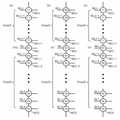
메모리 셀 어레이(10)는 다수의 비트라인(BLj, j=0~m), 다수의 워드라인(14. WL0 내지 WLn), 스트링 선택 라인(16, String Selecting Line; SSL), 그라운드 선택 라인(18, Ground Selecting Line; GSL), 공통 소스 라인(19, Common Souce Line; CSL), 스트링 선택 트랜지스터(String Selecting Transistor; SST), 그라운드 선택 트랜지스터(Ground Selecting Transistor; GST), 및 다수의 메모리 셀(MC0~MCn)을 포함한다.The
상기 스트링 선택 트랜지스터(SST)는 대응하는 비트라인(BLj, j=0~m)에 각각 접속되며 스트링 선택 라인(SSL)을 통하여 제어되고, 상기 그라운드 선택 트랜지스터(GST)는 상기 공통 소스 라인(CSL)과 접속되며 그라운드 선택 라인(GSL)을 통하 여 제어된다.The string select transistors SST are connected to corresponding bit lines BLj, j = 0 to m, respectively, and are controlled through a string select line SSL, and the ground select transistors GST are connected to the common source line CSL. ) And controlled via the ground select line (GSL).
상기 다수의 워드 라인(WL0 내지 WL31)은 상기 다수의 메모리 셀(MC0~MCn) 각각의 게이트에 접속되고, 대응되는 각각의 메모리 셀에 제어 전압을 인가한다.The plurality of word lines WL0 to WL31 are connected to gates of the plurality of memory cells MC0 to MCn, and a control voltage is applied to each of the corresponding memory cells.
상기 다수의 메모리 셀(MC0~MCn)은 상기 스트링 선택 트랜지스터(SST)와 상기 그라운드 선택 트랜지스터(GST) 사이에 직렬로 접속되어 하나의 스트링을 형성한다. 하나의 스트링을 형성하는 메모리 셀(MC0~MCn)의 개수(n+1)는 디바이스에 따라 16개, 32개, 64개로 구성될 수 있다.The plurality of memory cells MC0 to MCn are connected in series between the string select transistor SST and the ground select transistor GST to form one string. The number n + 1 of memory cells MC0 to MCn forming one string may be 16, 32, or 64 depending on the device.
상기 고전압 발생부(43)는 메모리 셀들을 프로그램, 소거, 및 리드시 필요한다수의 고전압을 생성한다. 상기 다수의 고전압은 제1, 제2 및 제3 검증전압(Vvfy1, Vvfy2, Vvfy3), 제1 리드 전압(Vr1), 제2 리드 전압(Vr2), 제1전압(Vread1), 제2전압(Vread2) 및 제3전압(Vread3)을 포함할 수 있다.The
도 8에 도시된 멀티레벨 메모리 셀의 문턱전압의 산포도를 함께 참조하여, 동작 모드에 따라 선택셀 및 비선택셀에 인가되는 전압에 대해 기술하면 다음과 같다.Referring to the scatter diagram of the threshold voltage of the multilevel memory cell illustrated in FIG. 8, the voltages applied to the selected cells and the non-selected cells according to the operation mode will be described as follows.
도 8을 참조하면, 메모리 셀은 2비트의 데이터를 저장할 수 있는 멀티레벨 메모리 셀(Multi Level Memory Cell)이다. 도 5에 도시된 NAND형 비휘발성 메모리 장치는 하나의 메모리 셀에 2비트의 데이터를 저장할 수 있는 멀티 레벨 셀로 구현될 수 있다. 2비트의 데이터("11", "10", "01", 및 "00")를 저장할 수 있는 메모리 셀은 프로그램 여부에 의해 4개의 문턱전압(Vt0, Vt1, Vt2, 및 Vt3) 산포를 가질 수 있다.Referring to FIG. 8, a memory cell is a multi level memory cell capable of storing two bits of data. The NAND type nonvolatile memory device illustrated in FIG. 5 may be implemented as a multilevel cell capable of storing two bits of data in one memory cell. A memory cell capable of storing two bits of data (“11”, “10”, “01”, and “00”) has four threshold voltages Vt0, Vt1, Vt2, and Vt3 depending on whether it is programmed or not. Can be.
일반적으로 데이터 기록되기 전에 비휘발성 메모리 장치의 상기 메모리 셀(MC0 내지 MCn)은 제1레벨(예컨대, "11")로 초기화되어 있으며, 제1레벨의 메모리 셀의 문턱전압은 음의 레벨을 가질 수 있다.In general, the memory cells MC0 to MCn of the nonvolatile memory device are initialized to a first level (eg, “11”) before data is written, and the threshold voltages of the memory cells of the first level have negative levels. Can be.
프로그램 검증시 상기 제1, 제2 또는 제3 검증전압(Vvfy1, Vvfy2, 또는 Vvfy3)이 상기 선택 셀에 인가되며, 상기 제1 전압(Vread1)은 상기 비선택 셀에 인가된다. 상기 선택 셀이 "10", "01", "00" 중 어느 상태로 프로그램되었는지에 따라 선택 셀에 인가되는 검증 전압은 상기 제1, 제2 또는 제3 검증전압(Vvfy1, Vvfy2, 또는 Vvfy3)이 될 수 있다.During the program verification, the first, second or third verification voltage Vvfy1, Vvfy2, or Vvfy3 is applied to the selected cell, and the first voltage Vread1 is applied to the unselected cell. The verification voltage applied to the selection cell may be the first, second or third verification voltage (Vvfy1, Vvfy2, or Vvfy3) depending on whether the selection cell is programmed to "10", "01", or "00". This can be
본 발명의 일 실시예에 따르면, 프로그램 검증 동작시에는 상기 선택셀에 검증전압(Vvfy1, Vvfy2, 또는 Vvfy3)이 인가되고 다수의 비선택 셀들에는 제1 전압(Vread1)이 인가될 수 있다. 이 경우, 리드 동작시에는 상기 선택 셀에 상기 제1 리드전압(Vr1) 또는 제2리드 전압(Vr2)이 인가되고, 상기 다수의 비선택 셀들에는 상기 제1 전압(Vread1)보다 높은 상기 제2전압(Vread2)이 인가될 수 있다. 이에 대해서는, 도 6을 참조하여 상세히 후술한다.According to an embodiment of the present invention, during the program verify operation, a verification voltage Vvfy1, Vvfy2, or Vvfy3 may be applied to the selected cells and a first voltage Vread1 may be applied to the plurality of unselected cells. In this case, during the read operation, the first read voltage Vr1 or the second lead voltage Vr2 is applied to the selected cell, and the second voltage higher than the first voltage Vread1 is applied to the plurality of unselected cells. The voltage Vread2 may be applied. This will be described later in detail with reference to FIG. 6.
본 발명의 다른 일 실시예에 따르면, 프로그램 검증 동작시에는 상기 선택 셀에 검증전압(Vvfy1, Vvfy2, 또는 Vvfy3)이 인가되고 다수의 비선택 셀들 중 선택셀의 드레인측에 연결되는 제1 그룹 비선택 셀들에는 제1 전압(Vread1)이 인가되고 다수의 비선택 셀들중 선택 셀의 소오스측에 연결되는 제2 그룹 비선택 셀들에는 제제1 전압(Vread1)보다 높은 제3 전압(Vread3)이 인가될 수 있다. 이 경우, 리드 동작시에는 상기 선택 셀에 상기 제1 리드전압(Vr1) 또는 제2리드 전압(Vr2)이 인 가되고, 상기 다수의 비선택 셀들에는 상기 제1 전압(Vread1) 보다 높은 상기 제2전압(Vread2)이 인가될 수 있다. 상기 제2 전압(Vread2)과 제3 전압(Vread3)은 같을 수 있다. 이에 대해서는, 도 7을 참조하여 상세히 후술한다.According to another embodiment of the present invention, in a program verifying operation, a verification voltage Vvfy1, Vvfy2, or Vvfy3 is applied to the selected cell and is a first group ratio connected to the drain side of the selected cell among a plurality of unselected cells. A first voltage Vread1 is applied to the selected cells and a third voltage Vread3 higher than the
한편, 상기 제1 리드전압(Vr1)은 상기 선택셀에 저장된 데이터가 "01"일때 상기 선택 셀에 인가되는 전압일 수 있고, 상기 제2 리드전압(Vr2)은 상기 선택셀에 저장된 데이터가 "10"일때 상기 선택 셀에 인가되는 전압일 수 있다.Meanwhile, the first read voltage Vr1 may be a voltage applied to the selected cell when the data stored in the selected cell is “01”, and the second read voltage Vr2 may be “the data stored in the selected cell”. When it is 10 "may be the voltage applied to the selected cell.
상기 제1 전압(Vread1)은 상기 선택된 메모리 셀의 해당 스트링 내에서의 순서(혹은 위치)에 따라 가변될 수 있다. 상기 가변되는 상기 제1 전압(Vread1)에 대한 상세한 설명 역시 도 6 내지 도 7을 참조하여 상세히 설명될 것이다.The first voltage Vread1 may vary according to an order (or position) in a corresponding string of the selected memory cell. A detailed description of the variable first voltage Vread1 will also be described in detail with reference to FIGS. 6 to 7.
상기 고전압 발생부(43)는 기준 전압을 펌핑하는 차지 펌프로 구현될 수 있다.The
상기 전압 선택부(45)는 고전압 발생부(43)로부터 출력되는 고전압들(Vvfy1, Vvfy2, Vvfy3, Vr1, Vr2, Vread1, Vread2, Vread3)을 수신하여, 동작 모드에 따라 어드레스 신호(AS1)와 제1제어신호(CS1)에 응답하여 상기 다수의 고전압을 선택적으로 다수의 워드라인(WL0 내지 WLn), 스트링 선택 라인(SSL), 및 그라운드 선택 라인(GSL)로 출력할 수 있다. 어드레스 신호(AS1)는 어드레스 버퍼(미도시) 혹은 어르데스 디코딩부(미도시)로부터 출력되는 신호일 수 있고, 제1제어신호(CS1)는 명령 신호를 판독하여 비휘발성 메모리 장치의 동작 모드를 결정하고 동작 모드에 따른 제어 신호들을 생성하는 제어부(미도시)로부터 발생될 수 있다. 동작 모드는 프로그램, 프로그램 검증, 리드, 소거 모드 중의 하나일 수 있다.The voltage selector 45 receives the high voltages Vvfy1, Vvfy2, Vvfy3, Vr1, Vr2, Vread1, Vread2, and Vread3 output from the
상기 리드 동작은 다수의 메모리 셀(MC0 내지 MCn) 각각에 저장된 데이터를 읽어내는 것이며, 상기 프로그램 검증 동작은 프로그램 후에 선택 셀(MCi)이 원하는 문턱전압값으로 프로그램되었는지를 검사하기 위한 동작이다. 상기 리드 동작과 상기 프로그램 검증 동작은 용도는 다르지만 실질적으로 모두 동일할 수 있다.The read operation is to read data stored in each of the plurality of memory cells MC0 to MCn, and the program verify operation is to check whether the selected cell MCi is programmed to a desired threshold voltage value after the program. The read operation and the program verify operation may be substantially the same although they have different uses.
상기 비휘발성 메모리 장치는 상기 선택 셀(MCi)이 충분히 프로그램되지 않았다면, 상기 선택 셀이 충분히 프로그램될 때까지 상기 프로그램, 및 프로그램 검증을 반복적으로 수행할 수 있다.If the selection cell MCi is not sufficiently programmed, the nonvolatile memory device may repeatedly perform the program and program verification until the selection cell is sufficiently programmed.
도 6은 본 발명의 일 실시예에 따른, 동작 모드에 따라 도 5에 도시된 메모리 셀에 인가되는 전압을 개념적으로 설명하기 위한 기능도이고, 도 7은 본 발명의 다른 일 실시예에 따른, 동작 모드에 따라 도 5에 도시된 메모리 셀에 인가되는 전압을 개념적으로 설명하기 위한 기능도이다.FIG. 6 is a functional diagram for conceptually describing a voltage applied to the memory cell shown in FIG. 5 according to an operation mode according to an embodiment of the present invention, and FIG. 7 is according to another embodiment of the present invention. This is a functional diagram for conceptually explaining a voltage applied to the memory cell shown in FIG. 5 according to an operation mode.
도 6 및 도 7에는 제1 메모리 셀(MC0)부터 제(n+1) 메모리 셀(MCn)까지 직렬로 연결된 하나의 스트링이 도시된다. 그리고, 제1 메모리 셀(MC0)부터 제(n+1) 메모리 셀(MCn) 순으로 순차적으로 프로그램되는 경우를 가정한다.6 and 7 illustrate one string connected in series from the first memory cell MC0 to the (n + 1) th memory cell MCn. In this case, it is assumed that the first memory cell MC0 is sequentially programmed from the (n + 1) th memory cell MCn.
도 6은 상기 선택된 메모리 셀(MCi)이 스트링내의 제1 메모리 셀(MC0)일 때, 즉, i=0일 때, 프로그램 검증을 위한 전압 조건 및 리드 동작을 위한 전압 조건을 나타낸다.6 illustrates a voltage condition for program verification and a voltage condition for read operation when the selected memory cell MCi is the first memory cell MC0 in a string, that is, i = 0.
도 6의 (a)를 참조하면, 프로그램 검증시 상기 전압 선택부(45)는 데이터(예컨대, "01")을 저장하고 있는 선택 셀(MC0)의 워드라인(WL0)에 검증 전압(Vvfy)을 출력하고, 비선택 셀(MC1~MCn)의 워드라인(WL1 내지 WLn)에 제1 전압(Vread)을 출 력한다. 제1 메모리 셀(MC0)를 선택하여 소정의 데이터(예컨대, "01")로 프로그램하고 상기 프로그램된 셀(MC0)에 대한 프로그램 검증을 하는 경우, 제2 내지 제(n+1) 메모리 셀들(MC1~MCn)은 아직 프로그램되기 전의 초기 상태("11")이다.Referring to FIG. 6A, during program verification, the voltage selector 45 may verify the voltage Vvfy on the word line WL0 of the selection cell MC0 that stores data (eg, “01”). The first voltage Vread is output to the word lines WL1 to WLn of the unselected cells MC1 to MCn. When the first memory cell MC0 is selected to be programmed with predetermined data (for example, "01") and the program verification is performed on the programmed cell MC0, the second through (n + 1) memory cells ( MC1-MCn) is the initial state ("11") before it is programmed.
도 6의 (b)를 참조하면, 리드 동작시 상기 전압 선택부(45)는 상기 선택된 메모리 셀(MC0)의 워드라인(WL0)에 제1 리드 전압(Vr1)을 출력하고, 상기 n개의 비선택 셀의 워드라인(WL1 내지 WLn)에 상기 제1 전압(Vread1)의 레벨보다 높은 레벨을 갖는 제2 전압(Vread2)을 출력한다. 리드 동작은 제(n+1) 메모리 셀(MCn)까지 모두 프로그램된 이후에 이루어질 수 있다. 제2 내지 제(n+1) 메모리 셀들(MC1~MCn)이 각각 가장 높은 문턱전압을 가지는 데이터(예컨대, "00")으로 프로그램된 경우가, 선택 셀(MC0)에 대한 프로그램 검증 동작시의 비선택 셀들의 채널 저항과 리드 동작시의 비선택 셀들의 채널 저항의 차이가 가장 많이 날 수 있는 경우이다. 따라서, 본 발명에서는 프로그램 검증 동작시 비선택 셀에 인가하는 제1 전압(Vread1)을 리드 동작시 비선택셀에 인가하는 제2 전압(Vread2)에 비하여 낮춤으로써, 프로그램 검증 동작시의 비선택셀들의 채널 저항과 리드 동작시의 비선택셀들의 채널 저항의 차이를 줄일 수 있다. 이로써, BPD 효과를 개선할 수 있다.Referring to FIG. 6B, in the read operation, the voltage selector 45 outputs the first read voltage Vr1 to the word line WL0 of the selected memory cell MC0 and outputs the n ratios. The second voltage Vread2 having a level higher than that of the first voltage Vread1 is output to the word lines WL1 to WLn of the selected cell. The read operation may be performed after all up to the (n + 1) th memory cells MCn are programmed. When the second to (n + 1) th memory cells MC1 to MCn are programmed with data having the highest threshold voltage (for example, "00"), the program verification operation for the selected cell MC0 is performed. This is the case where the difference between the channel resistance of the non-selected cells and the channel resistance of the non-selected cells during the read operation may be greatest. Therefore, in the present invention, the first voltage Vread1 applied to the non-selected cell during the program verify operation is lower than the second voltage Vread2 applied to the non-selected cell during the read operation, thereby reducing the non-selected cell during the program verify operation. It is possible to reduce the difference between the channel resistance of each channel and the channel resistance of unselected cells during read operation. Thereby, the BPD effect can be improved.
도 7은 상기 선택된 메모리 셀(MCi, i=0~n)이 스트링내의 임의의 위치에 위치하는 메모리 셀일 때, 프로그램 검증을 위한 전압 조건 및 리드 동작을 위한 전압 조건을 나타낸다.FIG. 7 illustrates a voltage condition for program verification and a voltage condition for read operation when the selected memory cell MCi (i = 0 to n) is a memory cell located at an arbitrary position in a string.
도 7의 (a)를 참조하면, 상기 비선택 셀들은 데이터가 프로그램되기 전인, 즉, 소거된 셀들로 이루어지는 제1 그룹 비선택셀(이하, 비선택된 제1 그룹 메모리 셀이라고도 함, MCi+1 내지 MCn)과 데이터가 프로그램된 셀들로 이루어지는 제2 그룹 비선택 셀(이하, 비선택된 제2 그룹 메모리 셀이라고도 함, MC0 내지 MCi-1)과 구분될 수 있다.Referring to FIG. 7A, the non-selected cells are first group non-selected cells (hereinafter, also referred to as unselected first group memory cells) formed before the data is programmed, that is, erased cells. To MCn) and a second group unselected cell (hereinafter, also referred to as an unselected second group memory cell, MC0 to MCi-1) including cells in which data is programmed.
상기 제1 그룹 비선택 셀(MCi+1 내지 MCn)은 상기 선택 셀(MCi)의 드레인측에 연결되는 (n-i)개의 메모리 셀을 포함하고, 제2 그룹 비선택셀(MC0 내지 MCi-1)은 상기 선택 셀(MCi)의 소오스 측에 연결되는 (i-1)개의 메모리 셀을 포함한다.The first group non-selected cells MCi + 1 to MCn include (ni) memory cells connected to the drain side of the selected cell MCi, and the second group non-selected cells MC0 to MCi-1. Includes (i-1) memory cells connected to the source side of the selection cell MCi.
상기 제1 그룹 비선택 셀(MCi+1 내지 MCn)은 프로그램 검증시에는 프로그램되기 전이고 리드 동작시에는 프로그램된 후이므로, 문턱전압의 차이로 인해 채널 저항이 달라져 상기 선택 셀(MCi)에 영향을 미친다. 그러나, 상기 제2 그룹 비선택 셀(MC0 내지 MCi-1)은 프로그램 검증시와 리드 동작시 모두 프로그램되어 있었으므로 상기 선택 셀(MCi)에 영향을 주지 않거나, 미약한 영향을 준다. 따라서, 프로그램 검증시 상기 제1 그룹 비선택 셀(MCi+1 내지 MCn)의 게이트에 인가하는 제1 전압(Vread1)과 상기 제2 그룹 비선택 셀(MC0 내지 MCi-1)의 게이트에 인가하는 제3 전압(Vread3)을 다르게 할 수 있다.Since the first group non-selected cells MCi + 1 to MCn are programmed before the program verification and after the read operation, the first group non-selected cells MCi + 1 to MCn are programmed during the read operation. Crazy However, since the second group non-selected cells MC0 to MCi-1 are programmed during both program verification and read operations, the second group non-selected cells MC0 to MCi-1 do not affect or have a slight effect on the selected cells MCi. Therefore, the first voltage Vread1 applied to the gates of the first group non-selected cells MCi + 1 to MCn and the gates of the second group non-selected cells MC0 to MCi-1 may be applied during program verification. The third voltage Vread3 may be different.
좀 더 구체적으로는, 프로그램 동작시, 상기 전압 선택부(45)는 제1제어신호(CS1)와 제1어드레스 신호(AS1)에 응답하여 상기 선택 셀(MCi)의 워드라인(WLi), 즉 상기 선택 셀(MCi)의 게이트에 검증전압(Vvfy)을 공급한다. 또한 전압 선택부(45)는 제1 그룹 비선택셀(MCi+1 내지 MCn)의 각 게이트에는 제1전압(Vread1)을 공급하고, 제2 그룹 비선택셀(MC0 내지 MCi-1)의 각 게이트에는 상기 제1전압(Vread1)의 레벨보다 큰 제3전압(Vread3)을 공급한다.More specifically, during the program operation, the voltage selector 45 may respond to the first control signal CS1 and the first address signal AS1 in response to the word line WLi of the selection cell MCi, that is, the word line WLi. The verification voltage Vvfy is supplied to the gate of the selection cell MCi. In addition, the voltage selector 45 supplies the first voltage Vread1 to each gate of the first group non-selected cells MCi + 1 to MCn, and supplies the first voltage Vread1 to each gate of the second group non-selected cells MC0 to MCi-1. The gate is supplied with a third voltage Vread3 that is greater than the level of the first voltage Vread1.
리드 동작시 상기 전압 선택부(45)는 상기 선택 셀(MCi)의 워드라인(WLi)에 제1 리드 전압(Vr1)을 출력한다. 또한, 상기 전압 선택부(45)는 리드 동작시 상기 제1 그룹 비선택 셀(MCi+1 내지 MCn)의 각 워드라인(WLi+1 내지 WLn)과 상기 제2 그룹 비선택 셀(MC0 내지 MCi-1)의 각 워드라인(WL0 내지 WLi-1)에 프로그램되어 있는 데이터에 상관없이 상기 제2 전압(Vread2)을 출력한다.In a read operation, the voltage selector 45 outputs a first read voltage Vr1 to the word line WLi of the select cell MCi. In addition, the voltage selector 45 may include the word lines WLi + 1 to WLn and the second group non-selected cells MC0 to MCi of the first group unselected cells MCi + 1 to MCn during a read operation. The second voltage Vread2 is output regardless of the data programmed in the word lines WL0 to WLi-1 of -1).
도 7의 (b)는, 상기 제1 그룹 비선택 셀(MCi+1 내지 MCn)이 모두 "00"으로 프로그램된 경우의 리드 동작시의 전압 인가 조건을 나타내고, 도 7의 (c)는, 상기 제1 그룹 비선택 셀(MCi+1 내지 MCn)이 모두 "11"로 프로그램된 경우의 리드 동작시의 전압 인가 조건을 나타낸다.FIG. 7B shows a voltage application condition during read operation when all of the first group non-selected cells MCi + 1 to MCn are programmed to "00", and FIG. The voltage application condition during the read operation when all of the first group non-selected cells MCi + 1 to MCn are programmed to "11" is shown.
도 7의 (b)의 경우에는, 선택 셀(MC0)에 대한 프로그램 검증 동작시의 비선택 셀들의 채널 저항과 리드 동작시의 비선택 셀들의 채널 저항의 차이가 많이 날 수 있지만, 제1 전압(Vread1)을 제2 전압(Vread2)에 비하여 낮춤으로써, 프로그램 검증 동작시의 비선택 셀들의 채널 저항과 리드 동작시의 비선택 셀들의 채널 저항의 차이를 줄여, BPD 효과를 개선할 수 있다. 제1 전압(Vread1)은 프로그램 검증 동작시의 비선택 셀들의 채널 저항과 리드 동작시의 비선택 셀들의 채널 저항이 거의 유사해질 수 있도록 실험적으로 혹은 시뮬레이션을 통해 결정될 수 있다.In the case of FIG. 7B, although the channel resistance of the unselected cells in the program verify operation with respect to the selected cell MC0 may differ from the channel resistance of the unselected cells in the read operation, the first voltage may vary. By lowering Vread1 to the second voltage Vread2, the difference between the channel resistance of the unselected cells in the program verify operation and the channel resistance of the unselected cells in the read operation can be reduced, thereby improving the BPD effect. The first voltage Vread1 may be determined experimentally or through simulation so that the channel resistance of the non-selected cells in the program verify operation and the channel resistance of the non-selected cells in the read operation may become substantially similar.
도 7의 (c)의 경우에는, 프로그램 검증 동작시와 리드 동작시 모두 제1 그룹 비선택셀(MCi+1 내지 MCn)의 데이터가 "11"로서 동일한데 리드 동작시 제1 그룹 비선택셀(MCi+1 내지 MCn)의 게이트에 인가되는 제2 전압(Vread2)가 프로그램 검증 동작시 제1 그룹 비선택셀(MCi+1 내지 MCn)의 게이트에 인가되는 제1 전압(Vread1) 보다 높다. 따라서, 프로그램 검증 동작시보다 리드 동작시의 비선택 셀들의 채널 저항이 줄어들어, 프로그램 검증 동작시보다 리드 동작시 선택 셀의 온셀 전류가 더 많이 흐를 수 있다. 그러나, 리드 동작시 온셀 전류가 더 많이 흐르는 것은 온셀/오프셀 판단에 오히려 유리한 효과를 줄 수 있으므로, 리드 마진에 악영향을 주지 않는다. 한편, 프로그램 검증 동작시보다 리드 동작시 선택 셀의 오프셀 전류 역시 증가할 수 있으나, 오프셀 전류의 변화량은 도 9b에 도시되듯이 미약하다.In FIG. 7C, the data of the first group non-selected cells MCi + 1 to MCn are the same as "11" in both the program verify operation and the read operation, but the first group non-selected cell in the read operation. The second voltage Vread2 applied to the gates of MCi + 1 to MCn is higher than the first voltage Vread1 applied to the gates of the first group unselected cells MCi + 1 to MCn during the program verify operation. Therefore, the channel resistance of the non-selected cells in the read operation is reduced than in the program verify operation, so that the on-cell current of the selected cell may flow more during the read operation than in the program verify operation. However, more on-cell current flowing during the read operation may have an advantageous effect on the on-cell / off-cell determination, and thus does not adversely affect the lead margin. On the other hand, the off-cell current of the selected cell may also increase during the read operation than during the program verify operation, but the amount of change in the off-cell current is weak as shown in FIG. 9B.
제1전압(Vread1)은 상기 선택된 메모리 셀(MCi)의 상기 스트링 내의 위치에 기초하여, 즉 i(i=0~n)에 따라 가변될 수 있다. 예컨대, 상기 제1전압(Vread1)은 상기 비선택된 제1 그룹 메모리 셀의 수(n-i)가 적을수록 상기 제2 전압(Vread2) 레벨과 가까워지도록 가변될 수 있다.The first voltage Vread1 may vary based on a position in the string of the selected memory cell MCi, that is, according to i (i = 0 to n). For example, the first voltage Vread1 may be changed to be closer to the second voltage Vread2 level as the number n-i of the unselected first group memory cells is smaller.
도 6 내지 도 7을 참조하면, 프로그램 검증시 도 6는 (n-1)개의 비선택 셀의 워드라인에 제1 전압이 인가되고 도 7은 (n-i)개의 제1 비선택 셀의 워드라인에 제1 전압(Vread1)이 인가된다. 제1 그룹 비선택 셀의 개수(n-i)가 감소할수록 프로그램 검증 동작시의 상기 비선택 셀의 채널 저항과 리드 동작시의 채널 저항이 유사해질 수 있다. 따라서, 제1 그룹 비선택 셀의 개수(n-i)가 감소할수록 상기 제1전압(Vread1)은 상기 제2 전압(Vread2) 레벨과 가까워지도록 가변될 수 있다.6 to 7, in the program verifying, FIG. 6 shows a first voltage applied to a word line of (n-1) unselected cells, and FIG. 7 shows a word line of (ni) first unselected cells. The first voltage Vread1 is applied. As the number n-i of the first group unselected cells decreases, the channel resistance of the unselected cells in the program verifying operation and the channel resistance in the read operation may become similar. Therefore, as the number n-i of the first group unselected cells decreases, the first voltage Vread1 may be changed to become closer to the second voltage Vread2 level.
상술한 도 6 및 도 7의 예는 상기 제1 메모리 셀(MC0)부터 상기 제(n+1) 메모리 셀(MCn)의 순으로 프로그램되는 경우이다.6 and 7 described above are cases where the first memory cell MC0 is programmed in order of the (n + 1) th memory cell MCn.
상기 제(n+1) 메모리 셀(MCn)부터 상기 제1 메모리 셀(MC0)의 순으로 프로그램되는 경우에는, 상기 제1 그룹 비선택 셀(MC0 내지 MCi-1)은 상기 선택 셀(MCi) 의 소오스측에 연결되는 (i-1)개의 메모리 셀을 포함하고, 제2 그룹 비선택셀(MCi+1 내지 MCn)은 상기 선택 셀(MCi)의 드레인 측에 연결되는 (n-i)개의 메모리 셀을 포함할 수 있다.When programmed in the order from the (n + 1) th memory cell MCn to the first memory cell MC0, the first group non-selected cells MC0 to MCi-1 are selected cells MCi. (I-1) memory cells connected to the source side of the second group non-selected cells MCi + 1 to MCn, and (ni) memory cells connected to the drain side of the selected cell MCi. It may include.
도 8은 도 5에 도시된 메모리 셀의 문턱전압의 산포도를 나타낸 그래프이다. 도 9a는 본 발명의 실시예에 따른 동작 모드에 따라 메모리 셀에 흐르는 전류 변화를 개념적으로 설명하기 위한 회로도이다. 도 9b는 본 발명의 실시예에 따른 동작 모드에 따라 메모리 셀에 흐르는 전류 변화를 나타낸 그래프이다.8 is a graph illustrating a scatter diagram of threshold voltages of the memory cell illustrated in FIG. 5. 9A is a circuit diagram for conceptually explaining a change in current flowing through a memory cell according to an operation mode according to an exemplary embodiment of the present invention. 9B is a graph illustrating a change in current flowing through a memory cell according to an operation mode according to an exemplary embodiment of the present invention.
도 9a를 참조하면, 프로그램 검증시 비선택 셀(예컨대, 프로그램되기 전의 제1 그룹 비선택 셀)에 인가되는 전압을 리드시 동작시 비선택 셀에 인가되는 전압에 비하여 낮춤으로써, 프로그램 검증 동작시 상기 비선택 셀의 채널 저항(Rinitial')과 리드 동작시 상기 비선택 셀의 채널 저항(Rafter)이 거의 유사해질 수 있다. 이 때, 리드 동작시 상기 비선택 셀의 채널 저항(Rafter)은 도 7의 (b)에 도시된 경우의 비선택 셀의 채널 저항일 수 있다. 이에 따라, 도 9b에 도시된 바와 같이, 리드 동작시 상기 선택 셀에 흐르는 온셀 전류(Icell') 혹은 오프셀 전류(Ioffcell')는 각각 프로그램 동작시 상기 선택 셀에 흐르는 온셀 전류(Icell") 혹은 오프셀 전류(Ioffcell")와 비교하여 유사하거나 그 변화량이 미약하게 줄어들 수 있다. 따라서, 리드 마진이 줄어들지 않는다.Referring to FIG. 9A, a voltage applied to an unselected cell (for example, a first group unselected cell before being programmed) may be lowered in comparison with a voltage applied to an unselected cell in a read operation. The channel resistance Rinitial 'of the unselected cell and the channel resistance Rafter of the unselected cell may become substantially similar during a read operation. In this case, the channel resistance Rafter of the unselected cell during the read operation may be the channel resistance of the unselected cell in the case shown in FIG. 7B. Accordingly, as shown in FIG. 9B, the on-cell current Icell 'or the off-cell current Ioffcell' flowing in the selected cell in the read operation may be the on-cell current Icell "flowing in the selected cell in the program operation, respectively. Compared with the off-cell current (Ioffcell "), the variation or the amount of change can be reduced slightly. Therefore, the lead margin does not decrease.
좀 더 구체적으로 설명하면, 도 7의 (a)에서 (b)로 변하는 경우, 본 발명은 상기 선택 셀의 프로그램 검증 동작은 다수의 비선택 셀에 제2전압보다 낮을 레벨을 갖는 제1전압(Vread1)을 인가함으로써 프로그램 검증시 상기 선택 셀에 흐르는 전류(Icell")는 리드 동작시 상기 선택 셀에 흐르는 전류(Icell')의 차이가 감소될 수 있다.More specifically, in the case of changing from (a) to (b) of FIG. 7, the present invention provides that the program verifying operation of the selected cell may include a first voltage having a level lower than a second voltage in a plurality of unselected cells. By applying Vread1), the difference between the current Icell 'flowing in the selected cell during program verification and the current Icell' flowing in the selected cell in read operation can be reduced.
한편, 도 7의 (a)에서 (c)로 변하는 경우에는 리드 동작시 상기 비선택 셀의 채널 저항이 도 4a에 도시된 채널 저항(Rinitil)과 유사해질 수 있다. 이 경우에는, 채널 저항의 감소로, 도 9b에 도시된 바와 같이, 리드 동작시 상기 선택 셀에 흐르는 온셀 전류(Icell) 혹은 오프셀 전류(Ioffcell)는 각각 프로그램 동작시 상기 선택 셀에 흐르는 온셀 전류(Icell") 혹은 오프셀 전류(Ioffcell")와 비교하여 증가할 수 있다. 그러나, 리드 동작시 온셀 전류의 증가는 리드 마진의 증가를 가져올 수 있으므로, 온셀/오프셀 판독에 유리할 수 있다.Meanwhile, in the case of changing from (a) to (c) of FIG. 7, the channel resistance of the unselected cell may become similar to the channel resistance Rinitil shown in FIG. 4A during a read operation. In this case, as shown in FIG. 9B, the on-cell current (Icell) or off-cell current (Ioffcell) flowing in the selected cell during the read operation is reduced by the channel resistance, respectively. (Icell ") or off-cell current (Ioffcell") may increase. However, an increase in on-cell current during read operation can lead to an increase in read margin, which can be advantageous for on-cell / off-cell reading.
상기 선택 셀이 오프 셀인 경우, 도 9b에 도시된 바와 같이 리드 동작시 상기 선택 셀에 흐르는 오프셀 전류(Ioffcell', Ioffcell)는 프로그램 검증시 상기 선택 셀에 흐르는 오프셀 전류(Ioffcell")와 전류값의 차이가 미미하므로 무시할 수 있다.When the selection cell is an off cell, as illustrated in FIG. 9B, the off-cell currents Ioffcell 'and Ioffcell flowing in the selection cell during the read operation are the off-cell current Ioffcell "and the current flowing in the selection cell during the program verification. The difference in values is negligible and can be ignored.
도 8을 참조하면, 메모리 셀에 데이터("01")를 프로그램한 직후, 상기 선택 셀의 문턱전압의 산포는 도 8의 "L1"과 같을 수 있다. 본 발명은 프로그램 검증시와 리드 동작시의 비선택 셀의 채널 저항의 저항값의 차이를 줄임으로써, 종래의 상기 선택 셀에 미치는 비선택 셀의 영향, 즉 BPD 효과를 감소시킬 수 있다. 따라서, 도 8에 도시된 바와 같이, 리드 동작시의 상기 선택 셀은 프로그램 검증시의 상기 선택 셀의 산포와 별 차이가 없는 "L3"와 같은 좁은 문턱전압의 산포도를 가질 수 있다.Referring to FIG. 8, immediately after programming data “01” in a memory cell, a distribution of threshold voltages of the selected cell may be the same as “L1” in FIG. 8. The present invention can reduce the difference of the resistance value of the channel resistance of the non-selected cell during the program verification and the read operation, thereby reducing the influence of the conventional non-selected cell on the selected cell, that is, the BPD effect. Therefore, as shown in FIG. 8, the selection cell in the read operation may have a narrow threshold voltage distribution such as "L3" which is not significantly different from the distribution of the selection cell in the program verification.
본 발명은 도면에 도시된 일 실시 예를 참고로 설명되었으나 이는 예시적인 것에 불과하며, 본 기술 분야의 통상의 지식을 가진 자라면 이로부터 다양한 변형 및 균등한 타 실시예가 가능하다는 점을 이해할 것이다. 따라서, 본 발명의 진정한 기술적 보호 범위는 첨부된 등록청구범위의 기술적 사상에 의해 정해져야 할 것이다.Although the present invention has been described with reference to one embodiment shown in the drawings, this is merely exemplary, and those skilled in the art will understand that various modifications and equivalent other embodiments are possible therefrom. Therefore, the true technical protection scope of the present invention will be defined by the technical spirit of the appended claims.
상술한 바와 같이 본 발명에 의하면, 프로그램 검증 동작시와 리드 동작시의 비선택 셀의 채널 저항의 차이를 줄임으로써, 프로그램 검증 동작시와 리드 동작시 선택 셀에 흐르는 전류의 변화가 줄어든다. 따라서, 리드마진이 충분히 확보됨으로써 상기 비휘발성 메모리 장치의 데이터 신뢰성이 향상될 있는 효과가 있다.As described above, according to the present invention, by reducing the difference between the channel resistances of the unselected cells during the program verify operation and the read operation, the change in the current flowing through the selected cell during the program verify operation and the read operation is reduced. Therefore, sufficient read margin is secured, thereby improving data reliability of the nonvolatile memory device.
Claims (18)
Translated fromKoreanPriority Applications (2)
| Application Number | Priority Date | Filing Date | Title |
|---|---|---|---|
| KR1020070059696AKR100882206B1 (en) | 2007-06-19 | 2007-06-19 | Nonvolatile Memory Device and Its Operation Method |
| US12/141,737US7773427B2 (en) | 2007-06-19 | 2008-06-18 | Non-volatile memory device and method of operating |
Applications Claiming Priority (1)
| Application Number | Priority Date | Filing Date | Title |
|---|---|---|---|
| KR1020070059696AKR100882206B1 (en) | 2007-06-19 | 2007-06-19 | Nonvolatile Memory Device and Its Operation Method |
Publications (2)
| Publication Number | Publication Date |
|---|---|
| KR20080111580A KR20080111580A (en) | 2008-12-24 |
| KR100882206B1true KR100882206B1 (en) | 2009-02-06 |
Family
ID=40136313
Family Applications (1)
| Application Number | Title | Priority Date | Filing Date |
|---|---|---|---|
| KR1020070059696AActiveKR100882206B1 (en) | 2007-06-19 | 2007-06-19 | Nonvolatile Memory Device and Its Operation Method |
Country Status (2)
| Country | Link |
|---|---|
| US (1) | US7773427B2 (en) |
| KR (1) | KR100882206B1 (en) |
Families Citing this family (12)
| Publication number | Priority date | Publication date | Assignee | Title |
|---|---|---|---|---|
| KR100865817B1 (en)* | 2007-02-14 | 2008-10-28 | 주식회사 하이닉스반도체 | Bit line selection voltage generator and read method of nonvolatile memory device using same |
| KR101259792B1 (en)* | 2007-07-10 | 2013-05-02 | 삼성전자주식회사 | Method for reading of NAND flash memory device |
| KR100908560B1 (en)* | 2007-08-06 | 2009-07-21 | 주식회사 하이닉스반도체 | Program method of flash memory device |
| US8051240B2 (en)* | 2008-05-09 | 2011-11-01 | Sandisk Technologies Inc. | Compensating non-volatile storage using different pass voltages during program-verify and read |
| KR100996108B1 (en)* | 2009-01-21 | 2010-11-22 | 주식회사 하이닉스반도체 | How to Program Nonvolatile Memory Devices |
| US7898864B2 (en)* | 2009-06-24 | 2011-03-01 | Sandisk Corporation | Read operation for memory with compensation for coupling based on write-erase cycles |
| KR101625641B1 (en)* | 2010-04-08 | 2016-05-30 | 삼성전자주식회사 | Non volatile memory device, operation method thereof, and devices having the nonvolatile memory device |
| JP2013069388A (en)* | 2011-09-26 | 2013-04-18 | Toshiba Corp | Nonvolatile semiconductor storage device |
| KR102015906B1 (en) | 2012-11-12 | 2019-08-29 | 삼성전자주식회사 | Memory system comprising nonvolatile memory device and read method tererof |
| KR20150093019A (en) | 2014-02-06 | 2015-08-17 | 에스케이하이닉스 주식회사 | Semiconductor memory device and operating method thereof |
| KR102423228B1 (en)* | 2015-09-17 | 2022-07-21 | 에스케이하이닉스 주식회사 | Storage device and operating method thereof |
| US11238933B2 (en) | 2018-02-26 | 2022-02-01 | Samsung Electronics Co., Ltd. | Non-volatile memory device including a verify circuit to control word and bit line voltages and method of operating the same |
Citations (2)
| Publication number | Priority date | Publication date | Assignee | Title |
|---|---|---|---|---|
| KR20050086290A (en)* | 2004-02-25 | 2005-08-30 | 주식회사 하이닉스반도체 | Method of verifying program for nand flash memory device |
| KR20070057716A (en)* | 2007-04-02 | 2007-06-07 | 김경섭 | Program method of flash memory device having multi-level cells |
Family Cites Families (6)
| Publication number | Priority date | Publication date | Assignee | Title |
|---|---|---|---|---|
| JPH0787039B2 (en) | 1987-12-28 | 1995-09-20 | 株式会社東芝 | Nonvolatile semiconductor memory device |
| US7149110B2 (en)* | 1999-01-14 | 2006-12-12 | Silicon Storage Technology, Inc. | Seek window verify program system and method for a multilevel non-volatile memory integrated circuit system |
| JP2000268593A (en) | 1999-03-18 | 2000-09-29 | Matsushita Electric Ind Co Ltd | Non-volatile semiconductor memory |
| US6907497B2 (en)* | 2001-12-20 | 2005-06-14 | Kabushiki Kaisha Toshiba | Non-volatile semiconductor memory device |
| KR20040008529A (en) | 2002-07-18 | 2004-01-31 | 주식회사 하이닉스반도체 | Circuit for verifying program/erase of cam cell in flashmemory |
| JP2006031871A (en)* | 2004-07-20 | 2006-02-02 | Toshiba Corp | Semiconductor memory device |
- 2007
- 2007-06-19KRKR1020070059696Apatent/KR100882206B1/enactiveActive
- 2008
- 2008-06-18USUS12/141,737patent/US7773427B2/enactiveActive
Patent Citations (2)
| Publication number | Priority date | Publication date | Assignee | Title |
|---|---|---|---|---|
| KR20050086290A (en)* | 2004-02-25 | 2005-08-30 | 주식회사 하이닉스반도체 | Method of verifying program for nand flash memory device |
| KR20070057716A (en)* | 2007-04-02 | 2007-06-07 | 김경섭 | Program method of flash memory device having multi-level cells |
Also Published As
| Publication number | Publication date |
|---|---|
| US20080316818A1 (en) | 2008-12-25 |
| KR20080111580A (en) | 2008-12-24 |
| US7773427B2 (en) | 2010-08-10 |
Similar Documents
| Publication | Publication Date | Title |
|---|---|---|
| KR100882206B1 (en) | Nonvolatile Memory Device and Its Operation Method | |
| US9087608B2 (en) | Method of programming non-volatile memory device and non-volatile memory device using the same | |
| KR100680479B1 (en) | Program Verification Method for Nonvolatile Memory Devices | |
| KR101198515B1 (en) | Operating method of semiconductor memory device | |
| KR101427896B1 (en) | A flash memory device for reducing noise in a common source line and a memory system including the same | |
| US8520435B2 (en) | Nonvolatile memory device and method of operating the same | |
| US8670273B2 (en) | Methods for program verifying a memory cell and memory devices configured to perform the same | |
| JP5931822B2 (en) | Nonvolatile semiconductor memory device | |
| US9536603B2 (en) | Methods and apparatuses for determining threshold voltage shift | |
| TWI569274B (en) | Sense operation in a stacked memory array device | |
| KR20040049114A (en) | Flash memory device having uniform threshold voltage distribution without under-programed or over-programed flash cells and program verify method thereof | |
| KR20130001442A (en) | Semiconductor memory device and method of operating the same | |
| KR20120059035A (en) | Program method of a semiconductor memory device | |
| JP2008091011A (en) | Flash memory element and program method thereof | |
| JP3961759B2 (en) | Nonvolatile semiconductor memory device | |
| KR20100106760A (en) | Non volatile memory device and programming method thereof | |
| KR20150035223A (en) | Semiconductor memory device and operating method thereof | |
| KR100898684B1 (en) | Flash memory device and program method thereof | |
| KR20120005817A (en) | Nonvolatile Memory Device and Its Operation Method | |
| KR20100016759A (en) | Method of operating a flash memory device | |
| US20240153568A1 (en) | Memory device related to verifying memory cells in an erase state and method of operating the memory device | |
| KR20080103362A (en) | Driving method of NAND flash memory device | |
| KR100936877B1 (en) | How to control the erase threshold voltage of flash device | |
| JP5081755B2 (en) | Nonvolatile semiconductor memory device and reading method thereof | |
| US12242732B2 (en) | Semiconductor apparatus with program operation control |
Legal Events
| Date | Code | Title | Description |
|---|---|---|---|
| A201 | Request for examination | ||
| PA0109 | Patent application | Patent event code:PA01091R01D Comment text:Patent Application Patent event date:20070619 | |
| PA0201 | Request for examination | ||
| E902 | Notification of reason for refusal | ||
| PE0902 | Notice of grounds for rejection | Comment text:Notification of reason for refusal Patent event date:20080528 Patent event code:PE09021S01D | |
| E701 | Decision to grant or registration of patent right | ||
| PE0701 | Decision of registration | Patent event code:PE07011S01D Comment text:Decision to Grant Registration Patent event date:20081126 | |
| PG1501 | Laying open of application | ||
| GRNT | Written decision to grant | ||
| PR0701 | Registration of establishment | Comment text:Registration of Establishment Patent event date:20090130 Patent event code:PR07011E01D | |
| PR1002 | Payment of registration fee | Payment date:20090130 End annual number:3 Start annual number:1 | |
| PG1601 | Publication of registration | ||
| PR1001 | Payment of annual fee | Payment date:20111229 Start annual number:4 End annual number:4 | |
| FPAY | Annual fee payment | Payment date:20130102 Year of fee payment:5 | |
| PR1001 | Payment of annual fee | Payment date:20130102 Start annual number:5 End annual number:5 | |
| FPAY | Annual fee payment | Payment date:20140103 Year of fee payment:6 | |
| PR1001 | Payment of annual fee | Payment date:20140103 Start annual number:6 End annual number:6 | |
| FPAY | Annual fee payment | Payment date:20141231 Year of fee payment:7 | |
| PR1001 | Payment of annual fee | Payment date:20141231 Start annual number:7 End annual number:7 | |
| FPAY | Annual fee payment | Payment date:20160104 Year of fee payment:8 | |
| PR1001 | Payment of annual fee | Payment date:20160104 Start annual number:8 End annual number:8 | |
| FPAY | Annual fee payment | Payment date:20170102 Year of fee payment:9 | |
| PR1001 | Payment of annual fee | Payment date:20170102 Start annual number:9 End annual number:9 | |
| FPAY | Annual fee payment | Payment date:20191226 Year of fee payment:12 | |
| PR1001 | Payment of annual fee | Payment date:20191226 Start annual number:12 End annual number:12 | |
| PR1001 | Payment of annual fee | Payment date:20201230 Start annual number:13 End annual number:13 | |
| PR1001 | Payment of annual fee | Payment date:20211229 Start annual number:14 End annual number:14 | |
| PR1001 | Payment of annual fee | Payment date:20221221 Start annual number:15 End annual number:15 | |
| PR1001 | Payment of annual fee | Payment date:20231226 Start annual number:16 End annual number:16 |