KR100881055B1 - Phase change memory unit, manufacturing method thereof, phase change memory device including same and manufacturing method thereof - Google Patents
Phase change memory unit, manufacturing method thereof, phase change memory device including same and manufacturing method thereofDownload PDFInfo
- Publication number
- KR100881055B1 KR100881055B1KR1020070060442AKR20070060442AKR100881055B1KR 100881055 B1KR100881055 B1KR 100881055B1KR 1020070060442 AKR1020070060442 AKR 1020070060442AKR 20070060442 AKR20070060442 AKR 20070060442AKR 100881055 B1KR100881055 B1KR 100881055B1
- Authority
- KR
- South Korea
- Prior art keywords
- lower electrode
- phase change
- filling member
- filling
- forming
- Prior art date
- Legal status (The legal status is an assumption and is not a legal conclusion. Google has not performed a legal analysis and makes no representation as to the accuracy of the status listed.)
- Active
Links
Images


Classifications
- H—ELECTRICITY
- H10—SEMICONDUCTOR DEVICES; ELECTRIC SOLID-STATE DEVICES NOT OTHERWISE PROVIDED FOR
- H10B—ELECTRONIC MEMORY DEVICES
- H10B41/00—Electrically erasable-and-programmable ROM [EEPROM] devices comprising floating gates
- H10B41/30—Electrically erasable-and-programmable ROM [EEPROM] devices comprising floating gates characterised by the memory core region
- H—ELECTRICITY
- H10—SEMICONDUCTOR DEVICES; ELECTRIC SOLID-STATE DEVICES NOT OTHERWISE PROVIDED FOR
- H10B—ELECTRONIC MEMORY DEVICES
- H10B63/00—Resistance change memory devices, e.g. resistive RAM [ReRAM] devices
- H—ELECTRICITY
- H10—SEMICONDUCTOR DEVICES; ELECTRIC SOLID-STATE DEVICES NOT OTHERWISE PROVIDED FOR
- H10B—ELECTRONIC MEMORY DEVICES
- H10B63/00—Resistance change memory devices, e.g. resistive RAM [ReRAM] devices
- H10B63/20—Resistance change memory devices, e.g. resistive RAM [ReRAM] devices comprising selection components having two electrodes, e.g. diodes
- H—ELECTRICITY
- H10—SEMICONDUCTOR DEVICES; ELECTRIC SOLID-STATE DEVICES NOT OTHERWISE PROVIDED FOR
- H10B—ELECTRONIC MEMORY DEVICES
- H10B63/00—Resistance change memory devices, e.g. resistive RAM [ReRAM] devices
- H10B63/30—Resistance change memory devices, e.g. resistive RAM [ReRAM] devices comprising selection components having three or more electrodes, e.g. transistors
- H—ELECTRICITY
- H10—SEMICONDUCTOR DEVICES; ELECTRIC SOLID-STATE DEVICES NOT OTHERWISE PROVIDED FOR
- H10B—ELECTRONIC MEMORY DEVICES
- H10B69/00—Erasable-and-programmable ROM [EPROM] devices not provided for in groups H10B41/00 - H10B63/00, e.g. ultraviolet erasable-and-programmable ROM [UVEPROM] devices
- H—ELECTRICITY
- H10—SEMICONDUCTOR DEVICES; ELECTRIC SOLID-STATE DEVICES NOT OTHERWISE PROVIDED FOR
- H10N—ELECTRIC SOLID-STATE DEVICES NOT OTHERWISE PROVIDED FOR
- H10N70/00—Solid-state devices having no potential barriers, and specially adapted for rectifying, amplifying, oscillating or switching
- H10N70/011—Manufacture or treatment of multistable switching devices
- H10N70/061—Shaping switching materials
- H10N70/063—Shaping switching materials by etching of pre-deposited switching material layers, e.g. lithography
- H—ELECTRICITY
- H10—SEMICONDUCTOR DEVICES; ELECTRIC SOLID-STATE DEVICES NOT OTHERWISE PROVIDED FOR
- H10N—ELECTRIC SOLID-STATE DEVICES NOT OTHERWISE PROVIDED FOR
- H10N70/00—Solid-state devices having no potential barriers, and specially adapted for rectifying, amplifying, oscillating or switching
- H10N70/20—Multistable switching devices, e.g. memristors
- H10N70/231—Multistable switching devices, e.g. memristors based on solid-state phase change, e.g. between amorphous and crystalline phases, Ovshinsky effect
- H—ELECTRICITY
- H10—SEMICONDUCTOR DEVICES; ELECTRIC SOLID-STATE DEVICES NOT OTHERWISE PROVIDED FOR
- H10N—ELECTRIC SOLID-STATE DEVICES NOT OTHERWISE PROVIDED FOR
- H10N70/00—Solid-state devices having no potential barriers, and specially adapted for rectifying, amplifying, oscillating or switching
- H10N70/801—Constructional details of multistable switching devices
- H10N70/821—Device geometry
- H10N70/826—Device geometry adapted for essentially vertical current flow, e.g. sandwich or pillar type devices
- H—ELECTRICITY
- H10—SEMICONDUCTOR DEVICES; ELECTRIC SOLID-STATE DEVICES NOT OTHERWISE PROVIDED FOR
- H10N—ELECTRIC SOLID-STATE DEVICES NOT OTHERWISE PROVIDED FOR
- H10N70/00—Solid-state devices having no potential barriers, and specially adapted for rectifying, amplifying, oscillating or switching
- H10N70/801—Constructional details of multistable switching devices
- H10N70/841—Electrodes
- H10N70/8413—Electrodes adapted for resistive heating
- H—ELECTRICITY
- H10—SEMICONDUCTOR DEVICES; ELECTRIC SOLID-STATE DEVICES NOT OTHERWISE PROVIDED FOR
- H10N—ELECTRIC SOLID-STATE DEVICES NOT OTHERWISE PROVIDED FOR
- H10N70/00—Solid-state devices having no potential barriers, and specially adapted for rectifying, amplifying, oscillating or switching
- H10N70/801—Constructional details of multistable switching devices
- H10N70/881—Switching materials
- H10N70/882—Compounds of sulfur, selenium or tellurium, e.g. chalcogenides
- H10N70/8825—Selenides, e.g. GeSe
- H—ELECTRICITY
- H10—SEMICONDUCTOR DEVICES; ELECTRIC SOLID-STATE DEVICES NOT OTHERWISE PROVIDED FOR
- H10N—ELECTRIC SOLID-STATE DEVICES NOT OTHERWISE PROVIDED FOR
- H10N70/00—Solid-state devices having no potential barriers, and specially adapted for rectifying, amplifying, oscillating or switching
- H10N70/801—Constructional details of multistable switching devices
- H10N70/881—Switching materials
- H10N70/882—Compounds of sulfur, selenium or tellurium, e.g. chalcogenides
- H10N70/8828—Tellurides, e.g. GeSbTe
Landscapes
- Engineering & Computer Science (AREA)
- Manufacturing & Machinery (AREA)
- Semiconductor Memories (AREA)
- Electrodes Of Semiconductors (AREA)
Abstract
Translated fromKoreanDescription
Translated fromKorean도 1a 내지 도 1d는 종래의 상변화 메모리 장치의 제조 방법을 설명하기 위한 단면도들이다.1A to 1D are cross-sectional views illustrating a method of manufacturing a conventional phase change memory device.
도 2는 본 발명의 실시예들에 따른 상변화 메모리 유닛을 설명하기 위한 단면도이다.2 is a cross-sectional view illustrating a phase change memory unit according to example embodiments.
도 3은 본 발명의 다른 실시예들에 따른 상변화 메모리 유닛들을 설명하기 위한 단면도이다.3 is a cross-sectional view illustrating phase change memory units according to other example embodiments of the inventive concept.
도 4a 내지 도 4h는 본 발명의 실시예들에 따른 상변화 메모리 유닛의 제조 방법을 설명하기 위한 단면도들이다.4A through 4H are cross-sectional views illustrating a method of manufacturing a phase change memory unit in accordance with embodiments of the present invention.
도 5a 내지 도 5c는 본 발명의 다른 실시예들에 따른 상변화 메모리 유닛의 제조 방법을 설명하기 위한 단면도들이다.5A through 5C are cross-sectional views illustrating a method of manufacturing a phase change memory unit according to other embodiments of the present invention.
도 6은 본 발명의 실시예들에 따른 상변화 메모리 장치들을 설명하기 위한 단면도이다.6 is a cross-sectional view illustrating phase change memory devices in accordance with example embodiments of the inventive concept.
도 7은 본 발명의 다른 실시예들에 따른 상변화 메모리 장치들을 설명하기 위한 단면도이다.7 is a cross-sectional view illustrating phase change memory devices in accordance with other example embodiments of the inventive concept.
도 8은 본 발명의 또 다른 실시예들에 따른 상변화 메모리 장치들을 설명하기 위한 단면도이다.8 is a cross-sectional view illustrating phase change memory devices in accordance with some example embodiments of the present invention.
도 9는 본 발명의 또 다른 실시예들에 따른 상변화 메모리 장치들을 설명하기 위한 단면도이다.9 is a cross-sectional view illustrating phase change memory devices in accordance with some example embodiments of the present invention.
도 10a 내지 도 10h는 본 발명의 실시예들에 따른 상변화 메모리 장치의 제조 방법을 설명하기 위한 단면도들이다.10A through 10H are cross-sectional views illustrating a method of manufacturing a phase change memory device according to example embodiments.
도 11a 내지 도 11c는 본 발명의 다른 실시예들에 따른 상변화 메모리 장치의 제조 방법을 설명하기 위한 단면도들이다.11A through 11C are cross-sectional views illustrating a method of manufacturing a phase change memory device in accordance with some example embodiments of the present invention.
도 12a 내지 도 12i는 본 발명의 또 다른 실시예들에 따른 상변화 메모리 장치의 제조 방법을 설명하기 위한 단면도들이다.12A to 12I are cross-sectional views illustrating a method of manufacturing a phase change memory device according to still other embodiments of the present invention.
도 13은 본 발명의 실시예들에 따른 전극 구조체를 설명하기 위한 단면도이다.13 is a cross-sectional view for describing an electrode structure according to example embodiments.
도 14는 본 발명의 다른 실시예들에 따른 전극 구조체를 설명하기 위한 단면도이다.14 is a cross-sectional view for describing an electrode structure according to example embodiments.
<도면의 주요 부분에 대한 부호의 설명><Explanation of symbols for the main parts of the drawings>
100, 200, 300, 500: 기판245: 도전성 구조물100, 200, 300, 500: substrate 245: conductive structure
255, 355, 595: 스페이서255, 355, 595: spacer
265, 267, 365, 367, 605, 607: 하부 전극265, 267, 365, 367, 605, 607: lower electrode
267a, 367a, 617a: 제1 하부 전극막 패턴267a, 367a, and 617a: first lower electrode film pattern
267b, 367b, 617b: 제2 하부 전극막 패턴267b, 367b, and 617b: second lower electrode film patterns
277, 377, 617: 충진 구조물277, 377, 617: filling structures
277a, 377a, 617a: 제1 충진 부재277a, 377a, 617a: first filling member
277b, 377b, 617b: 제2 충진 부재249, 349, 585: 오믹층277b, 377b, and 617b: second filling
280, 380, 620: 상변화 물질층 패턴290, 390, 630: 상부 전극280, 380, 620: Phase change
345: 다이오드420, 544: 제1 배선345:
450, 660: 제2 배선510: 게이트 구조물450 and 660: second wiring 510: gate structure
본 발명은 상변화 메모리 유닛, 이의 제조 방법, 이를 포함하는 상변화 메모리 장치 및 그 제조 방법에 관한 것이다. 보다 상세하게는, 개선된 구조의 충진 부재를 포함하는 상변화 메모리 유닛, 이의 제조 방법, 이를 포함하는 상변화 메모리 장치 및 그 제조 방법에 관한 것이다.The present invention relates to a phase change memory unit, a manufacturing method thereof, a phase change memory device including the same, and a manufacturing method thereof. More particularly, the present invention relates to a phase change memory unit including a filling member having an improved structure, a manufacturing method thereof, a phase change memory device including the same, and a manufacturing method thereof.
반도체 메모리 장치는 대체로 전원 공급이 중단 되었을 경우에 저장된 데이터의 유지 여부에 따라 일반적으로 DRAM 장치 또는 SRAM 장치와 같은 휘발성 반도체 메모리 장치와 플래시 메모리 장치 또는 EEPROM 장치와 같은 비휘발성 반도체 메모리 장치로 구분될 수 있다. 디지털 카메라, 휴대폰 또는 MP3 플레이어와 같은 전자 기기에 사용되는 반도체 메모리 장치로서는 비휘발성 메모리 장치인 플래시 메모리 장치가 주로 사용되고 있다. 그러나 플래시 메모리 장치는 데이터를 기록하 거나 기록된 데이터를 읽는 과정에서 비교적 많은 시간이 요구되기 때문에, 플래시 메모리 장치를 대체하기 위하여 MRAM 장치, FRAM 장치 또는 PRAM 장치와 같은 새로운 반도체 장치가 개발되었다.In general, a semiconductor memory device may be classified into a volatile semiconductor memory device such as a DRAM device or an SRAM device and a nonvolatile semiconductor memory device such as a flash memory device or an EEPROM device, depending on whether or not the stored data is maintained when a power supply is interrupted. have. As a semiconductor memory device used in an electronic device such as a digital camera, a mobile phone or an MP3 player, a flash memory device which is a nonvolatile memory device is mainly used. However, since flash memory devices require a relatively long time to write data or read recorded data, new semiconductor devices such as MRAM devices, FRAM devices, or PRAM devices have been developed to replace flash memory devices.
일반적으로 상변화 메모리(PRAM) 장치는 상변화 물질층을 구성하는 칼코겐(chalcogenide) 화합물의 상전이에 따른 비정질 상태와 결정 상태 사이의 저항의 차이를 이용하여 데이터를 저장한다. 즉, 상변화 메모리 장치는 인가된 펄스의 진폭과 길이에 따라 칼코겐 화합물로 이루어진 상변화 물질층의 가역적 상변화를 이용하여 데이터를 "0" 과 "1"의 상태로 저장한다. 예를 들면, 저항이 큰 비정질 상태로의 전환에 요구되는 리셋 전류(reset current)와 저항이 작은 결정 상태로 바꾸는 셋 전류(set current)는 기판 상에 형성된 트랜지스터 혹은 다이오드로부터 하부 전극을 거쳐 상변화 물질층으로 전달되어 상변화 물질층의 상변화를 유발한다. 이러한 상변화 메모리 장치들에 있어서, 트랜지스터 또는 다이오드를 스위칭 소자로 구비하는 구조에 따라 트랜지스터형 상변화 메모리 장치 및 다이오드형 상변화 메모리 장치로 구분할 수 있다. 전술한 종래의 트랜지스터형 또는 다이오드형 상변화 메모리 장치들은 한국등록특허 제642645호, 한국등록특허 제655796호, 미국공개특허 제2006/0284237호 및 일본공개특허 제2007-019559호 등에 개시되어 있다.In general, a phase change memory (PRAM) device stores data using a difference in resistance between an amorphous state and a crystalline state due to a phase transition of a chalcogenide compound constituting a phase change material layer. That is, the phase change memory device stores data in the states of "0" and "1" by using a reversible phase change of a phase change material layer made of a chalcogenide compound according to the amplitude and length of an applied pulse. For example, the reset current required for the transition to the amorphous state with a high resistance and the set current for changing to a crystalline state with a low resistance may be phase changed from the transistor or diode formed on the substrate via the lower electrode. It is transferred to the material layer to cause a phase change of the phase change material layer. In such phase change memory devices, a transistor type phase change memory device and a diode type phase change memory device may be classified according to a structure including a transistor or a diode as a switching element. The above-described conventional transistor type or diode type phase change memory devices are disclosed in Korean Patent No. 642645, Korean Patent No. 655796, US Patent Publication No. 2006/0284237, Japanese Patent Publication No. 2007-019559, and the like.
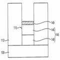
도 1a 내지 도 1d는 종래의 다이오드형 상변화 메모리 장치의 제조 방법을 설명하기 위한 단면도들이다.1A to 1D are cross-sectional views illustrating a method of manufacturing a conventional diode type phase change memory device.
도 1a를 참조하면, 소자 분리 공정을 이용해 반도체 기판(100) 상에 소자 분리막(도시하지 않음)을 형성한 후, 반도체 기판(100)의 액티브 영역에 불순물을 주 입하여 불순물 영역(도시하지 않음)을 형성한다.Referring to FIG. 1A, after forming an isolation layer (not shown) on the
반도체 기판(100) 상에 실리콘 산화물을 사용하여 상기 불순물 영역을 노출시키는 개구(115)를 갖는 층간 절연막(112)을 형성한다. 반도체 기판(100)을 시드로 이용하는 선택적 에피택시얼 성장(SEG) 공정을 수행하여, 개구(115)를 매립하는 실리콘막을 형성한 다음, 상기 실리콘막의 상부를 제거하여 개구(115)를 부분적으로 매립하는 실리콘막 패턴을 형성한다.An
상기 실리콘막 패턴의 상부에 제1 불순물들을 주입하여 상부 실리콘막 패턴(146)을 형성하고, 상기 실리콘막 패턴의 하부에 제2 불순물들을 주입하여 하부 실리콘막 패턴(148)을 형성한다. 이에 따라, 개구(115) 내에는 다이오드(145)가 형성된다. 상부 및 하부 실리콘막 패턴(146, 148)을 포함하는 다이오드(145) 상에 코발트 실리사이드로 구성된 오믹층(149)을 형성한다.An upper
도 1b를 참조하면, 오믹층(149), 개구(115)의 저면과 측벽 및 층간절연막(112) 상에 실리콘 질화물을 사용하여 스페이서용 절연막을 형성한 후, 상기 스페이서용 절연막을 식각하여 개구(115)의 측벽 상에 스페이서(155)를 형성한다. 스페이서(155)가 형성되면 오믹층(149)이 노출된다.Referring to FIG. 1B, after forming an insulating film for a spacer using silicon nitride on the
도 1c를 참조하면, 노출된 오믹층(149), 스페이서(155) 및 층간 절연막(112) 상에 티타늄막(162) 및 티타늄 질화막(164)을 순차적으로 적층하여 하부 전극층(160)을 형성한 다음, 하부 전극층(160) 상에 실리콘 질화물을 사용하여 충진막(170)을 형성한다. 하부 전극층(160)은 개구(115)를 부분적으로 채우며, 충진막(170)은 개구(115)를 완전히 채운다.Referring to FIG. 1C, the
도 1d를 참조하면, 충진막(170)과 하부 전극층(160)을 층간 절연막(112)이 노출될 때까지 제거하여, 개구(115)를 매립하는 충진 부재(175) 및 하부전극(165)을 형성한다. 여기서, 하부 전극(165)은 티타늄막 패턴(166) 및 티타늄 질화막 패턴(168)으로 이루어진다.Referring to FIG. 1D, the
충진 부재(175), 하부 전극(165), 스페이서(155) 및 층간 절연막(112) 상에 상변화 물질층 패턴(180) 및 상부 전극(190)을 형성한다. 상변화 물질층 패턴(180)은 칼코겐 화합물을 사용하여 형성되며, 상부 전극(190)은 주로 금속을 사용하여 형성된다.The phase change
전술한 종래의 다이오드형 상변화 메모리 장치의 제조 방법에 있어서, 도핑된 실리콘막 패턴들(146, 148)을 포함하는 다이오드(145)로부터 금속으로 이루어진 하부 전극(165)으로 전류가 용이하게 흐르도록 코발트 실리사이드로 구성된 오믹층(149)을 형성한다. 또한, 칼코겐 화합물을 포함하는 상변화 물질층 패턴(190)의 상전이를 효과적으로 일으키기 위하여, 실리콘 질화물로 구성된 스페이서(155)를 통해 하부 전극(165)과 상변화 물질층 패턴(190) 사이의 접촉 면적을 감소시킨다. 더욱이, 하부 전극(165)과 상변화 물질층 패턴(190) 사이의 접촉 면적을 더욱 감소시키기 위해서, 하부 전극(165)의 내부를 매립하도록 실리콘 질화물로 이루어진충진 부재(175)를 형성한다. 그러나, 스페이서(155)와 충진 부재(175)가 각기 오믹층(149) 및 하부 전극(165) 상에 대략 680C 이상의 고온에서 실리콘 질화물을 사용하여 형성되기 때문에, 오믹층(149)이 열적 손상을 입게 되어, 상기 상변화 메모리 장치에 이른 바 싱글 비트 페일(single bit fail) 현상이 발생한다. 특히, 충진 막(170)을 형성하는 공정에서 오믹층(149)에 발생하는 손상이 스페이서용 절연막(150)을 형성하는 과정에서 오믹층(149)에야기되는 손상보다 크게 나타난다. 이와 같이 오믹층(149)에 열적 손상이 발생하면, 상기 상변화 메모리 장치의 전기적인 특성이 크게 저하되는 문제가 야기된다.In the above-described method of manufacturing a diode type phase change memory device, a current easily flows from the
따라서, 본 발명의 일 목적은 오믹층의 손상을 방지하여 개선된 전기적인 특성과 신뢰성을 확보할 수 있는 상변화 메모리 유닛 및 그 제조 방법을 제공하는 것이다.Accordingly, it is an object of the present invention to provide a phase change memory unit and a method of manufacturing the same, which can prevent damage to the ohmic layer and ensure improved electrical characteristics and reliability.
본 발명의 다른 목적은 오믹층의 손상을 방지하여 개선된 전기적인 특성과 신뢰성을 갖는 상변화 메모리 장치 및 그 제조 방법을 제공하는 것이다.Another object of the present invention is to provide a phase change memory device having improved electrical characteristics and reliability by preventing damage to an ohmic layer and a method of manufacturing the same.
상술한 본 발명의 일 목적을 달성하기 위하여, 본 발명의 실시예들에 따른 상변화 메모리 유닛은, 기판을 노출시키는 개구를 갖는 절연 구조물, 상기 개구 내에 형성되는 도전성 구조물, 상기 도전성 구조물 상에 형성되며, 리세스를 갖는 하부 전극, 상기 리세스를 채우는 적어도 하나의 충진 부재, 상기 하부 전극 및 상기 적어도 하나의 충진 부재 상에 형성되는 상변화 물질층 패턴, 그리고 상기 상변화 물질층 패턴 상에 형성되는 상부 전극을 포함한다.In order to achieve the above object of the present invention, a phase change memory unit according to embodiments of the present invention, an insulating structure having an opening for exposing a substrate, a conductive structure formed in the opening, formed on the conductive structure And a lower electrode having a recess, at least one filling member filling the recess, a phase change material layer pattern formed on the lower electrode and the at least one filling member, and a phase change material layer pattern. And an upper electrode.
본 발명의 실시예들에 있어서, 상기적어도 하나의 충진 부재는, 상기 하부 전극의 리세스를 부분적으로 채우는 제1 충진 부재 및 상기 제1 충진 부재 상에 형성되며, 상기 리세스를 채우는 제2 충진 부재를 포함할 수 있다. 이 경우, 상기 제 1 충진 부재와 상기 제2 충진 부재는 서로 다른 물질을 포함할 수 있다. 예를 들면, 상기 제1 충진 부재는 폴리실리콘을 포함할 수 있으며, 상기 제2 충진 부재는 실리콘 질화물과 같은 질화물 또는 실리콘 산화물과 같은 산화물을 포함할 수 있다.In embodiments of the present invention, the at least one filling member is formed on the first filling member and the first filling member partially filling the recess of the lower electrode, and the second filling filling the recess. It may include a member. In this case, the first filling member and the second filling member may include different materials. For example, the first filling member may include polysilicon, and the second filling member may include a nitride such as silicon nitride or an oxide such as silicon oxide.
본 발명의 실시예들에 있어서, 상기 도전성 구조물과 상기 하부 전극 사이에 금속 실리사이드를 포함하는 오믹층이 더 개재될 수 있다. 또한, 상기 하부 전극의 측면에 접촉되는 스페이서가 형성될 수 있다.In example embodiments, an ohmic layer including a metal silicide may be further interposed between the conductive structure and the lower electrode. In addition, a spacer may be formed in contact with the side of the lower electrode.
본 발명의 실시예들에 있어서, 상기 하부 전극은, 상기 도전성 구조물에 접촉되는 제1 하부 전극막 패턴 및 상기 적어도 하나의 충진 부재에 접촉되는 제2 하부 전극막 패턴을 포함할 수 있다. 이 경우, 상기 제2 하부 전극막 패턴은 상기 제1 하부 전극막 패턴 보다 높은 비저항을 가질 수 있다. 예를 들면, 상기 제2 하부 전극막 패턴은 금속질화물 또는 금속 산화물을 포함할 수 있고, 상기 제1 하부전극막 패턴은 금속을 포함할 수 있다.In example embodiments, the lower electrode may include a first lower electrode layer pattern contacting the conductive structure and a second lower electrode layer pattern contacting the at least one filling member. In this case, the second lower electrode film pattern may have a higher resistivity than the first lower electrode film pattern. For example, the second lower electrode film pattern may include metal nitride or metal oxide, and the first lower electrode film pattern may include metal.
본 발명의 실시예들에 있어서, 상기 도전성 구조물은 다이오드, 패드, 콘택 또는 플러그를 포함할 수 있다.In embodiments of the present invention, the conductive structure may include a diode, a pad, a contact, or a plug.
전술한 본 발명의 일 목적을 달성하기 위하여, 본 발명의 실시예들에 따른 전극 구조체는, 리세스를 갖는 전극, 상기 리세스를 부분적으로 채우는 제1 충진 부재, 그리고 상기 제1 충진 부재 상에 형성되며, 상기 리세스를 채우는 제2 충진 부재를 포함한다. 상기 전극, 제1 전극막 패턴과 상기 제1 전극막 패턴 상에 형성되며, 상기 제2 충진 부재에 접촉되는 제2 전극막 패턴을 포함할 수 있다.In order to achieve the above object of the present invention, the electrode structure according to the embodiments of the present invention, the electrode having a recess, the first filling member to partially fill the recess, and on the first filling member And a second filling member filling the recess. The electrode may include a second electrode film pattern formed on the electrode, the first electrode film pattern, and the first electrode film pattern and in contact with the second filling member.
상술한 본 발명의 다른 목적을 달성하기 위하여, 본 발명의 실시예들에 따른 상변화 메모리 장치는, 불순물 영역을 갖는 기판, 상기 기판 상에 형성되며, 상기 불순물 영역을 노출시키는 개구를 갖는 층간 절연막, 상기 개구 내에 형성되는 도전성 구조물, 상기 도전성 구조물 상에 형성되며, 리세스를 갖는 하부 전극, 상기 리세스를 부분적으로 채우는 제1 충진 부재, 상기 제1 충진 부재 상에 형성되며, 상기 리세스를 채우는 제2 충진 부재, 상기 하부 전극, 상기 제2 충진 부재 및 상기 절연 구조물 상에 형성되는 상변화 물질층 패턴, 그리고 상기 상변화 물질층 패턴 상에 형성되는 상부 전극을 포함한다.In order to achieve the above object of the present invention, a phase change memory device according to embodiments of the present invention, a substrate having an impurity region, an interlayer insulating film formed on the substrate and having an opening exposing the impurity region And a conductive structure formed in the opening, a lower electrode formed on the conductive structure, a lower electrode having a recess, a first filling member partially filling the recess, and formed on the first filling member. And a phase filling material layer pattern formed on the second filling member, the lower electrode, the second filling member and the insulating structure, and an upper electrode formed on the phase change material layer pattern.
상술한 본 발명의 일 목적을 달성하기 위하여, 본 발명의 실시예들에 따른 상변화 메모리 유닛의 제조 방법에 있어서, 기판을 노출시키는 개구를 갖는 절연 구조물을 형성하고, 상기 개구 내에 도전성 구조물을 형성한 후, 상기 도전성 구조물 상에 리세스를 갖는 하부 전극을 형성한다. 상기 리세스를 채우는 적어도 하나의 충진 부재를 형성한 다음, 상기하부 전극, 상기 적어도 하나의 충진 부재 및 상기 절연 구조물 상에 상변화 물질층 패턴을 형성하고, 상기 상변화 물질층 패턴 상에 상부 전극을 형성한다.In order to achieve the above object of the present invention, in the manufacturing method of the phase change memory unit according to the embodiments of the present invention, forming an insulating structure having an opening for exposing the substrate, and forming a conductive structure in the opening Thereafter, a lower electrode having a recess is formed on the conductive structure. Forming at least one filling member filling the recess, and then forming a phase change material layer pattern on the lower electrode, the at least one filling member and the insulating structure, and forming an upper electrode on the phase change material layer pattern To form.
본 발명의 실시예들에 따른 상기 적어도 하나의 충진 부재를 형성하는 단계에 있어서, 상기 하부 전극의 리세스를 부분적으로 채우는 제1 충진 부재를 형성한 다음, 상기 제1 충진 부재 상에 상기 리세스를 채우는 제2 충진 부재를 형성할 수 있다. 상기 제1 충진 부재는 상기 하부 전극 상에 폴리실리콘을 화학 기상 증착(CVD) 공정으로 증착하여 형성될 수 있다.In the forming of the at least one filling member according to embodiments of the present invention, after forming a first filling member partially filling the recess of the lower electrode, the recess is formed on the first filling member. It is possible to form a second filling member to fill the. The first filling member may be formed by depositing polysilicon on the lower electrode by a chemical vapor deposition (CVD) process.
본 발명의 실시예들에 있어서, 상기 제2 충진 부재는 상기 제1 충진 부재로부터 형성될 수 있다. 예를 들면, 상기 제2 충진 부재는 상기 제1 충진 부재의 상부를 질화 또는 산화시켜 형성될 수 있다. 또한, 상기 상변화 물질층 패턴을 형성하기 전에, 상기 하부 전극의 상부를 질화 또는 산화시킬 수 있다. 이 경우, 상기 제1 충진 부재의 상부와 하부 전극의 상부는 동시에 질화 또는 산화될 수 있다.In embodiments of the present invention, the second filling member may be formed from the first filling member. For example, the second filling member may be formed by nitriding or oxidizing an upper portion of the first filling member. In addition, before forming the phase change material layer pattern, an upper portion of the lower electrode may be nitrided or oxidized. In this case, the upper portion of the first filling member and the upper portion of the lower electrode may be nitrided or oxidized at the same time.
본 발명의 실시예들에 있어서, 상기 하부 전극을 형성하기 전에, 상기도전성 구조물 상에 오믹층을 형성할 수 있다. 또한, 상기 하부 전극을 형성하기 전에, 상기 도전성 구조물 상에 상기 개구의 측벽에 접촉되는 스페이서를 형성할 수 있다.In embodiments of the present invention, before forming the lower electrode, an ohmic layer may be formed on the conductive structure. In addition, before forming the lower electrode, a spacer may be formed on the conductive structure to contact the sidewall of the opening.
또한, 상술한 본 발명의 다른 목적을 달성하기 위하여, 본 발명의 실시예들에 따른 상변화 메모리 장치의 제조 방법에 있어서, 기판에 불순물 영역을 형성하고, 상기 기판 상에, 상기 불순물 영역을 노출시키는 개구를 갖는 층간 절연막을 형성한 다음, 상기 개구 내에 상에 도전성 구조물을 형성한다. 상기 도전성 구조물 상에 리세스를 갖는 하부 전극을 형성하고, 상기 하부 전극 상에 리세스 부분적으로 채우는 제1 충진 부재를 형성한 후, 상기 제1 충진 부재 상에 상기 리세스를 채우는 제2 충진 부재를 형성한다. 상기 하부 전극, 상기 제2 충진 부재 및 상기 층간 절연막 상에 상변화 물질층 패턴을 형성한 다음, 상기 상변화 물질층 패턴 상에 상부 전극을 형성한다.In addition, in order to achieve the above object of the present invention, in the method of manufacturing a phase change memory device according to embodiments of the present invention, an impurity region is formed on a substrate, and the impurity region is exposed on the substrate. An interlayer insulating film having an opening to be formed is formed, and then a conductive structure is formed on the opening. A second filling member forming a lower electrode having a recess on the conductive structure and forming a first filling member partially filling the recess on the lower electrode, and then filling the recess on the first filling member To form. A phase change material layer pattern is formed on the lower electrode, the second filling member, and the interlayer insulating layer, and then an upper electrode is formed on the phase change material layer pattern.
본 발명에 따르면, 상기 상변화 메모리 유닛에는 절연성 물질 뿐만 아니라 도전성 물질을 포함하는 충진 구조물도 사용될 수 있다. 즉, 도전성 물질로 제1 충진 부재를 형성하더라도, 상기 제1 충진 부재 상에 절연성 제2 충진 부재를 더 형 성함으로써, 하부 전극이 상변화 물질층 패턴을 가열하는 효율을 증대시킬 수 있다. 이에 따라, 상기 상변화 메모리 유닛을 포함하는 상변화 메모리 장치의 리셋 전류 감소 효과를 얻을 수 있다. 특히, 상기 제1 충진 부재로서 종래의 실리콘 질화물 대신에 폴리실리콘을 사용함으로써, 상기 충진 구조물 형성 시에 오믹층이 받는 열적 손상을 줄일 수 있다. 또한, 하부 전극의 상부를 질화 처리하여 비저항을 높임으로써, 상기 상변화 물질층 패턴을 가열하는 효율을 높여 상기 리셋 전류를 감소시킬 수 있다.According to the present invention, a filling structure including a conductive material as well as an insulating material may be used for the phase change memory unit. That is, even when the first filling member is formed of the conductive material, by further forming the insulating second filling member on the first filling member, the efficiency of heating the phase change material layer pattern of the lower electrode may be increased. Accordingly, the reset current reduction effect of the phase change memory device including the phase change memory unit may be obtained. In particular, by using polysilicon instead of conventional silicon nitride as the first filling member, it is possible to reduce thermal damage to the ohmic layer when forming the filling structure. In addition, by nitriding the upper portion of the lower electrode to increase specific resistance, the reset current may be reduced by increasing the efficiency of heating the phase change material layer pattern.
이하, 첨부된 도면들을 참조하여 본 발명의 실시예들에 따른 상변화 메모리 유닛, 이의 제조 방법, 이를 포함하는 상변화 메모리 장치 및 그 제조 방법에 대하여 상세하게 설명하지만, 본 발명이 하기의 실시예들에 제한되는 것은 아니며, 해당 분야에서 통상의 지식을 가진 자라면 본 발명의 기술적 사상을 벗어나지 않는 범위 내에서 본 발명을 다양한 다른 형태로 구현할 수 있을 것이다. 첨부된 도면에 있어서, 기판, 층(막), 전극, 영역, 패드, 패턴 또는 구조물의 치수는 본 발명의 명확성을 기하기 위하여 실제보다 확대하여 도시한 것이다. 본 발명에 있어서, 각 층(막), 영역, 전극, 플러그, 패드, 패턴 또는 구조물이 기판, 각 층(막), 영역, 전극, 플러그, 패드 또는 패턴의 "상에", "상부에" 또는 "하부"에 형성되는 것으로 언급되는 경우에는 각 층(막), 영역, 전극, 플러그, 패드, 패턴 또는 구조물이 직접 기판, 각 층(막), 영역, 패드 또는 패턴 위에 형성되거나 아래에 위치하는 것을 의미하거나, 다른 층(막), 다른 영역, 다른 패드, 다른 전극, 다른 패턴 또는 다른 구조물이 기판 상에 추가적으로 형성될 수 있다. 또한, 물질, 가스, 층(막), 영역, 패드, 전극, 패턴 또는 구조물이 "예비", "제1", "제2" 및/또는 "제3"으로 언급되는 경우, 이러한 부재들을 한정하기 위한 것이 아니라 단지 각 물질, 가스, 화합물, 층(막), 영역, 전극, 플러그, 패드, 패턴 또는 구조물을 구분하기 위한 것이다. 따라서 "예비", "제1", "제2" 및/또는 "제3"은 물질, 가스, 층(막), 영역, 전극, 플러그, 패드, 패턴 또는 구조물에 대하여 각기 선택적으로 또는 교환적으로 사용될 수 있다. 한편, 실질적으로 동일하거나 유사한 구성 부재들에 대해서는 동일한 참조 부호를 사용한다.Hereinafter, a phase change memory unit, a manufacturing method thereof, a phase change memory device including the same, and a manufacturing method thereof according to embodiments of the present invention will be described in detail with reference to the accompanying drawings. The present invention is not limited thereto, and one of ordinary skill in the art may implement the present invention in various other forms without departing from the technical spirit of the present invention. In the accompanying drawings, the dimensions of the substrate, layer (film), electrode, region, pad, pattern or structure are shown to be larger than the actual for clarity of the invention. In the present invention, each layer (film), region, electrode, plug, pad, pattern or structure is "on" and "on" a substrate, each layer (film), region, electrode, plug, pad or pattern. Or where it is said to be formed "under", each layer (film), region, electrode, plug, pad, pattern, or structure is directly formed over or below the substrate, each layer (film), region, pad, or pattern. Alternatively, another layer (film), another region, another pad, another electrode, another pattern or other structure may be additionally formed on the substrate. Also, when a material, gas, layer (film), region, pad, electrode, pattern or structure is referred to as "preliminary", "first", "second" and / or "third", such members are defined. It is not intended to distinguish each substance, gas, compound, layer (film), region, electrode, plug, pad, pattern or structure. Thus, the "preliminary", "first", "second" and / or "third" are selective or interchangeable with respect to materials, gases, layers (films), regions, electrodes, plugs, pads, patterns or structures, respectively. Can be used as On the other hand, the same reference numerals are used for substantially the same or similar components.
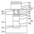
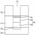
도 2는 본 발명의 실시예들에 따른 상변화 메모리 유닛을 설명하기 위한 단면도이다.2 is a cross-sectional view illustrating a phase change memory unit according to example embodiments.
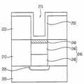
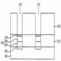
도 2를 참조하면, 상기 상변화 메모리 유닛은, 트렌치(trench)(269) 또는 그루브(groove)를 갖는 하부 전극(265), 충진 구조물(277), 상변화 물질층 패턴(280) 및 상부전극(290)을 구비한다. 하부 전극(265)의 측벽에는 스페이서(255)가 제공되며, 하부 전극(265) 아래에는 오믹층(249)이 위치한다.Referring to FIG. 2, the phase change memory unit may include a
상기 상변화 메모리 유닛은 기판(200) 상에 형성된다. 기판(200)은 실리콘 기판, 게르마늄 기판, 실리콘-게르마늄 기판,SOI(silicon on insulator) 기판, GOI(germanium on insulator) 기판 등과 같은반도체 기판을 포함할 수 있다. 본 발명의 실시예들에 있어서, 기판(200)에는 제1 불순물이 도핑된 불순물 영역(205)이 형성될 수 있다. 또한, 기판(200) 상에는 불순물 영역(205), 패드, 콘택, 플러그, 게이트 구조물 및/또는 트랜지스터를 포함하는 하부 구조물이 형성될 수 있다.The phase change memory unit is formed on the
기판(200) 상에는 불순물 영역(205)을 노출시키는 제1 개구를 갖는 제1 층간 절연막(212)이 형성된다. 제1 층간 절연막(212)은 BPSG, PSG, USG, SOG, FOX, TEOS, PE-TEOS, HDP-CVD 산화물 등과 같은 실리콘 산화물을 포함할 수 있다.A first
상기 제1 개구 내의 불순물 영역(205) 상에는 도전성 구조물(245)이 제공된다. 도전성 구조물(205)은 제1 층간 절연막(212)에 형성된 상기 개구의 하부를 채운다. 도전성 구조물(245)은 콘택, 패드, 플러그, 도전막 패턴, 다이오드, 게이트 구조물 및/또는트랜지스터를 포함할 수 있다. 본 발명의 실시예들에 있어서, 도전성 구조물(245)은 다이오드를 포함할 수 있다. 이 경우, 도전성 구조물(245)은 불순물 영역(205) 상에 순차적으로 형성된 상부도전막 패턴(246) 및 하부 도전막 패턴(248)을 구비한다. 상부 및 하부 도전막 패턴(246, 248)은 기판(200)을 시드(seed)로 이용하는 선택적 에피택시얼 성장(SEG) 공정을 통해 형성될 수 있다. 따라서, 상부 및 하부 도전막 패턴(246, 248)은 각기 실리콘을 포함할 수 있다. 즉, 기판(200)이 실리콘을 포함하는 경우, 상부 및 하부 도전막 패턴(246, 248)도 실리콘을 포함할 수 있다. 또한, 상부 도전막 패턴(246)은 불순물 영역(205)의 상기 제1 불순물들과 상이한 도전형을 갖는 제2 불순물들을 포함할 수 있으며, 하부 도전막 패턴(248) 상기 제1 불순물들과 동일한 도전형을 갖는 제3 불순물들을 포함할 수 있다. 예를 들어, 상기 제1 및 제3 불순물들은 각기 N형의도전형을 가질 수 있고, 상기 제2 불순물들은 P형의 도전형을 가질 수 있다. 또한, 상부 도전막 패턴(246)은 상대적으로 높은 불순물 농도를 가질 수 있으며, 하부 도전막 패턴(248)은 상대적으로 낮은 불순물 농도를 가질 수 있다.A
본 발명의 다른 실시예들에 따르면, 도전성 구조물(245)은 적어도 하나의 도 전성 플러그 또는 패드를 포함할 수 있다. 여기서, 상기 도전성 플러그 또는 패드는 불순물이 도핑된 실리콘, 금속 또는 금속 질화물 등으로 이루어질 수 있다.According to other embodiments of the present invention, the
오믹층(249)은 도전성 구조물(245)과 하부전극(265) 사이에 형성된다. 하부 전극(265)이 금속을 포함하는 경우, 오믹층(249)은 금속실리사이드를 포함할 수 있다. 예를 들어, 하부 전극(265)이 티타늄, 텅스텐, 탄탈륨 또는 코발트를 포함하는 경우, 오믹층(249)은 티타늄 실리사이드, 텅스텐 실리사이드, 탄탈륨 실리사이드 또는 코발트 실리사이드로 이루어질 수 있다. 오믹층(249)은 도전성 구조물(245)로부터 하부 전극(265)으로 원활하게 전류가 흐를 수 있도록 한다.The
제1 층간 절연막(212) 상에는 오믹층(249)을 노출시키는 제2 개구를 갖는 제2 층간 절연막(222)이 형성된다. 제2 층간 절연막(222)은 산화물, 질화물 또는 산질화물을 포함할 수 있다. 예를 들면, 제2 층간 절연막(222)은 실리콘 산화물, 실리콘 질화물 또는 실리콘 산질화물을 포함할 수 있다. 본 발명의 실시예들에 있어서, 제2 층간 절연막(222)은 제1 층간 절연막(212)과 실질적으로 동일한 물질을 포함할 수 있으나, 제1 및 제2 층간 절연막(212, 222)은 서로 상이한 물질로 이루어질 수도 있다.A second
하부 전극(265)은 제2 층간 절연막(212)의 상기 제2 개구를 채우면서 오믹층(249) 상에 형성된다. 하부 전극(265)에는 소정의 치수를 갖는 트렌치(269) 또는 리세스가 제공된다. 본 발명의 실시예들에 있어서, 하부 전극(265)은 실린더의 구조, 중공형 다각 기둥 구조, 컵의 구조 등과 같은 입체 구조를 가질 수 있다. 하부 전극(265)은 금속이나 금속 화합물을 포함할 수 있다. 예를 들어, 하부 전극(265) 은 텅스텐, 알루미늄, 구리, 탄탈륨, 티타늄, 몰리브덴, 니오븀, 지르코늄, 알루미늄 질화물, 티타늄 알루미늄 질화물, 티타늄 질화물, 텅스텐 질화물, 탄탈륨 질화물, 몰리브덴 질화물, 몰리브덴 티타늄 질화물, 몰리브덴 알루미늄 질화물, 니오븀 질화물, 티타늄 보론 질화물, 텅스텐 보론 질화물, 지르코늄 알루미늄 질화물, 탄탈륨 또는 탄탈륨 알루미늄 질화물 지르코늄 실리콘 질화물, 탄탈륨 실리콘 질화물, 몰리브덴 실리콘 질화물, 텅스텐 실리콘 질화물, 티타늄 실리콘 질화물 등을 포함할 수 있다. 이들은 단독으로 또는 서로 혼합되어 사용될 수 있다. 본 발명의 다른 실시예들에 따르면, 하부 전극(265)은 금속막, 금속 질화막 및/또는 금속 실리콘 질화막을 포함하는 복합막 구조를 가질 수 있다.The
충진 구조물(277)은 제1 충진 부재(277a) 및 제2 충진 부재(277b)를 포함하며, 트렌치(269)를 매립하면서 하부 전극(265) 상에 형성된다. 제1 충진 부재(277a)는 하부 전극(265)의 트렌치(269)를 부분적으로 매립할 수 있으며, 제2 충진 부재(277b)는 트렌치(268)를 완전히 채울 수 있다. 즉, 트렌치(269)의 하부 및 상부는 각기 제1 및 제2 충진 부재(277a, 277b)에 의해 채워질 수 있다.The filling
제1 충진 부재(277a)는 도전성 물질 혹은 절연성 물질을 포함할 수 있다. 본 발명의 실시예들에 있어서, 제1 충진 부재(277a)는 폴리실리콘, 아몰퍼스 실리콘, 단결정 실리콘, 불순물이 도핑된 폴리실리콘, 불순물이 도핑된 아몰퍼스 실리콘, 불순물이 도핑된 단결정 실리콘 등을 포함할 수 있다. 제2 충진 부재(277b)는 제1 충진 부재(277a) 상에 형성된다. 제2 충진 부재(277b)는 트렌치(269)의 상부를 채울 수 있다. 제2 충진 부재(277b)는 절연성 물질을 포함할 수 있다. 예를 들면, 제 2 충진 부재(277b)는 실리콘 질화물과 같은 질화물이나 실리콘 산화물 등의 산화물을 포함할 수 있다.The
충진 구조물(277)에 의해 하부 전극(265)과 상변화 물질층 패턴(280) 사이의 접촉 면적이 감소되기 때문에, 상대적으로 작은 리셋 전류로도 효율적으로 상기 상변화 메모리 유닛의 상변화 물질층 패턴(280)을 가열할 수 있다. 이 때, 충진 구조물(277) 전체가 절연성 물질일 필요는 없으며, 상변화 물질층(280)에 접촉되는 제2 충진 부재(277b)만이 절연성 물질을 포함하는 것으로 충분하다.Since the contact area between the
하부 전극(265)과 상기 제2 개구의 측벽 사이에는 스페이서(255)가 형성된다. 즉, 하부 전극(265)을 스페이서(255)가 감싸게 된다. 스페이서(255)는 실리콘 질화물과 같은 질화물 또는 실리콘 산질화물 등의 산질화물을 포함할 수 있다. 제2 층간 절연막(222)과 스페이서(255)가 실질적으로 동일한 물질을 포함하는 경우, 스페이서(255)는 제2 층간 절연막(222)과 일체로 형성될 수 있다.A
본 발명의 실시예들에 따르면, 스페이서(255)의 폭에 따라 하부 전극(265)과 상변화 물질층 패턴(280) 사이의 접촉 면적이 변동된다. 즉, 스페이서(255)의 폭의 증감에 따라 하부 전극(265)과 상변화 물질층 패턴(280) 사이의 접촉 면적이 증가하거나 감소될 수 있다.According to embodiments of the present invention, the contact area between the
이에 따라, 하부 전극(265)을 통해 상변화 물질층 패턴(280)을 가열하기 위해 인가되는리셋 전류를 스페이서(255)의 폭에 의해용이하게 조절할 수 있다.Accordingly, the reset current applied to heat the phase change
상변화 물질층 패턴(280)은 하부전극(265), 충진 구조물(277), 스페이서(255) 및 제2 층간 절연막(222) 상에형성된다. 상변화 물질층 패턴(280)은 칼코 겐 화합물을 포함할 수 있다. 예를 들면, 상변화 물질층 패턴(280)은 게르마늄-안티몬-텔루르를 포함하는 GST 화합물로 구성되거나, 탄소, 질소 및/또는 금속이 도핑된GST 화합물로 이루어질 수 있다. 여기서, 상변화 물질층 패턴(280)에 포함되는 금속으로는 티타늄, 니켈, 지르코늄, 몰리브덴, 루테늄, 팔라듐, 하프늄, 탄탈륨, 이리듐, 백금 등을 들 수 있다. 이들은 단독으로 또는 서로 혼합되어 사용될 수 있다.The phase change
하부 전극(265)을 통해 인가되는 전류에 의해가열됨으로써, 상변화 물질층 패턴(280)을 구성하는 칼코겐 화합물의 상전이가 발생된다. 즉, 상변화 물질층 패턴(280)이 가열되는 정도에 따라, 상변화 물질층 패턴(280)을 구성하는 물질이 비정질 상태 혹은 결정 상태를 가질 수 있으며, 이러한 상태에 대응되는 데이터들이 저장될 수 있다.The phase transition of the chalcogenide compound constituting the phase change
상부 전극(290)은 상변화 물질층 패턴(280) 상에 형성된다. 상부 전극(290)은 금속, 도핑된 폴리실리콘 및/또는 금속 화합물을 포함한다. 본 발명의 실시예들에 따르면, 상부 전극(290)은 상변화 물질층 패턴(280) 상에 차례로 형성된 제1 상부 전극막 패턴(도시되지 않음) 및 제2 상부 전극막 패턴(도시되지 않음)을 포함할 수 있다. 이 경우, 상기 제1 상부 전극막 패턴은 금속을 포함할 수 있으며, 상기 제2 상부 전극막 패턴은 도전성 금속 질화물 혹은 도전성 금속 실리콘 질화물을 포함할 수 있다. 예를 들면, 상기 제1 상부 전극막 패턴은 티타늄, 니켈, 지르코늄, 몰리브덴, 루테늄, 팔라듐, 하프늄, 탄탈륨, 이리듐, 백금 등을 포함할 수 있다. 이들은 단독으로 또는 서로 혼합되어 사용될 수 있다. 또한, 상기 제2 상부 전극막 패턴은 티타늄 질화물, 니켈 질화물, 지르코늄 질화물, 몰리브덴 질화물, 루테늄 질화물, 팔라듐 질화물, 하프늄 질화물, 탄탈륨 질화물, 이리듐 질화물, 백금 질화물, 텅스텐 질화물, 알루미늄 질화물, 니오븀 질화물, 티타늄 실리콘 질화물, 티타늄 알루미늄 질화물, 티타늄 보론 질화물, 지르코늄 실리콘 질화물, 텅스텐 실리콘 질화물, 텅스텐 보론 질화물, 지르코늄 알루미늄 질화물, 몰리브덴 실리콘 질화물, 몰리브덴 알루미늄 질화물, 탄탈륨 실리콘 질화물, 탄탈륨 알루미늄 질화물 등을 포함할 수 있다. 이들은 단독으로 또는 서로 혼합되어 사용될 수 있다.The
본 발명의 실시예들에 있어서, 상기 상변화 메모리 유닛은 절연성 물질뿐만 아니라 도전성 물질을 포함하는 충진 구조물(277)을 포함할 수 있다. 즉, 도전성 물질로 제1 충진 부재(277a)를 형성하더라도, 제1 충진 부재(277a) 상에 절연성 물질로 구성된 제2 충진 부재(277b)를 형성하여 상변화 물질층 패턴(280)을 가열효율을 증대시킬 수 있다. 이에 따라, 상기 상변화 메모리 유닛의 리셋 전류를 감소시킬 수 있다. 특히, 제1 충진 부재(277a)로서 종래의 실리콘 질화물 대신에 폴리실리콘을 사용하는 경우, 충진 구조물(277) 형성 시에 오믹층(249)이 받는 열적 손상을 크게 감소시킬 수 있다.In example embodiments, the phase change memory unit may include a filling
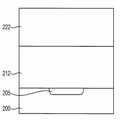
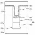
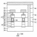
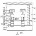
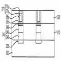
도 3은 본 발명의 다른 실시예들에 따른 상변화 메모리 유닛들을 설명하기 위한 단면도이다. 도 3에 도시한 상기 상변화 메모리 유닛은, 하부 전극(267)을 제외하면 도 2를 참조하여 설명한 상변화 메모리 유닛과 실질적으로 동일한 구조를 가진다.3 is a cross-sectional view illustrating phase change memory units according to other example embodiments of the inventive concept. The phase change memory unit illustrated in FIG. 3 has a structure substantially the same as that of the phase change memory unit described with reference to FIG. 2 except for the
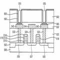
도 3을 참조하면, 상기 상변화 메모리 유닛은, 트렌치(269) 또는 그루브를 갖는 하부 전극(267), 제1 및 제2 충진 부재(277a, 277b)를 포함하는 충진 구조물(277), 스페이서(255), 오믹층(249), 상변화 물질층 패턴(280) 그리고 상부 전극(290)을 구비한다.Referring to FIG. 3, the phase change memory unit may include a filling
상기 상변화 메모리 유닛은 기판(200) 상에 제공되며, 기판(200)에는 불순물 영역(205)이 형성된다. 제1 층간 절연막(212)은 이러한 불순물 영역(205)을 덮으면서 기판(200) 상에 형성된다. 제1 층간 절연막(212)에는 불순물 영역(205)을 노출시키는 제1 개구가 형성된다.The phase change memory unit is provided on a
상기 상변화 메모리 유닛은 상기 제1 개구 내에 형성된 도전성 구조물(245)을 구비한다. 도전성 구조물(245)은 하부 도전막 패턴(248) 및 상부 도전막 패턴(246)을 포함한다. 오믹층(249)은 상부 도전막 패턴(246) 상에 위치한다. 제1 층간 절연막(212)의 제1 개구는 도전성 구조물(245) 및 오믹층(249)에 의해 채워지게 된다.The phase change memory unit has a
제1 층간 절연막(212) 상에는 제2 층간 절연막(222)이 형성된다. 제2 층간 절연막(222)은 오믹층(249)을 노출시키는 제2 개구를 가진다.The second
하부 전극(267)은 제2 층간 절연막(222)의 제2 개구를 부분적으로 채우면서 오믹층(249) 상에 형성된다. 하부 전극(267)에는 트렌치(269) 또는 리세스가 제공되며, 제1 및 제2 충진 부재(277a, 277b)를 포함하는 충진 구조물(277)는 이와 같은 트렌치(269) 또는 리세스를 채우게 된다. 본 발명의 실시예들에 있어서, 하부 전극(267)은 중공형의 실린더 형상, 중공형의 다각 기둥 형상, 컵의 형상 등과 같은 입체 구조를 가질 수 있다.The
하부 전극(267)은 오믹층(249)에 접촉되는 제1 하부 전극막 패턴(267a)과 제1 하부 전극막 패턴(267a) 상에 위치하는 제2 하부 전극막 패턴(267b)을 구비한다. 제1 하부 전극막 패턴(267a)은 충진 구조물(277)의 하부를 감사며, 충진 구조물(277)의 상부는 제2 하부 전극막 패턴(267b)에 의해 둘러싸인다.The
제1 하부 전극막 패턴(267a)은 금속, 금속 질화물, 금속 실리콘 질화물 등을 포함할 수 있다. 예를 들면, 제1 하부 전극막 패턴(267a)은 텅스텐, 알루미늄, 구리, 탄탈륨, 티타늄, 몰리브덴, 니오븀, 지르코늄, 알루미늄 질화물, 티타늄 알루미늄 질화물, 티타늄 질화물, 텅스텐 질화물, 탄탈륨 질화물, 몰리브덴 질화물, 몰리브덴 티타늄 질화물, 몰리브덴 알루미늄 질화물, 니오븀 질화물, 티타늄 보론 질화물, 텅스텐 보론 질화물, 지르코늄 알루미늄 질화물, 탄탈륨 또는 탄탈륨 알루미늄 질화물 지르코늄 실리콘 질화물, 탄탈륨 실리콘 질화물, 몰리브덴 실리콘 질화물, 텅스텐 실리콘 질화물, 티타늄 실리콘 질화물 등을 포함할 수 있다. 본 발명의 다른 실시예들에 있어서, 제1 하부 전극막 패턴(267a)은 금속막/금속 질화막 혹은 금속막/금속 실리콘 질화막을 포함하는 복합막 구조를 가질 수 있다.The first lower
제2 하부 전극막 패턴(267b)은 제1 하부 전극막 패턴(267a) 상에 형성되며, 충진 구조물(277)의 상부 측면에 접촉된다. 즉, 제2 하부 전극막 패턴(267b)은 충진 구조물(277) 상부를 감싸는 형상을 가질 수 있다. 도 3에는제2 하부 전극막 패턴(267b)의 두께가 제2 충진 부재(277b)의 두께에 비하여 얇은 것으로 도시되어 있으나, 제2 하부 전극막 패턴(267b)의 두께는 제2 충진 부재(277b)의 두께와 실질적으로 동일하거나 더 두꺼울 수 있다.The second lower
제2 하부 전극막 패턴(267b)은 제1 하부 전극막 패턴(267a)에 비해 높은 비저항을 갖는 물질을 포함할 수 있다. 본 발명의 실시예들에 있어서, 제2 하부 전극막 패턴(267b)은 금속 질화물 또는 금속 실리콘 질화물을 포함할 수 있다. 예를 들어, 제2 하부 전극막 패턴(267b)은 티타늄 알루미늄 질화물, 알루미늄 질화물, 티타늄 질화물, 텅스텐 질화물, 탄탈륨 질화물, 몰리브덴 질화물, 몰리브덴 티타늄 질화물, 니오븀 질화물, 티타늄 실리콘 질화물, 티타늄 보론 질화물, 지르코늄 실리콘 질화물, 텅스텐 실리콘 질화물, 텅스텐 보론 질화물, 지르코늄 알루미늄 질화물, 몰리브덴 실리콘 질화물, 몰리브덴 알루미늄 질화물, 탄탈륨 실리콘 질화물 또는 탄탈륨 알루미늄 질화물 등을 포함할 수 있다. 본 발명의 다른 실시예들에 있어서, 제2 하부 전극막 패턴(267b)은 도전성 금속 산화물을 포함할 수 있다.The second lower
하부 전극(267)의 측벽과 상기 제2 개구의 내벽 사이에는 스페이서(255)가 위치한다. 따라서, 제2 층간 절연막(222)의 제2 개구는 스페이서(255), 하부 전극(267) 및 충진 구조물(277)에 의해 매립된다.The
상변화 물질층 패턴(280)은 제2 층간 절연막(222), 스페이서(255), 하부 전극(267) 및 충진 구조물(277) 상에 위치하며, 상부 전극(290)은 상변화 물질층 패턴(280) 상에 배치된다.The phase change
전류는 도전성 구조물(245)과 하부전극(267)을 통해 상변화 물질층 패턴(280)으로 인가됨으로써, 상변화 물질층 패턴(280)을 구성하는 물질의 상전이가 유도된다. 이 때, 제2 하부 전극막 패턴(267b)이 금속에 비해 상대적으로 높은 비저항을 갖는 금속 질화물, 금속 실리콘 질화물 또는 도전성 금속 산화물을 포함하 기 때문에, 작은 전류로도 상변화 물질층 패턴(280)을 효율적으로 가열할 수 있다. 이에 따라, 상기 상변화 메모리 유닛의 리셋 전류를 크게 감소시킬 수 있다.The current is applied to the phase change
도 4a 내지 도 4h는 본 발명의 실시예들에 따른 상변화 메모리 유닛의 제조 방법을 설명하기 위한 단면도들이다. 도 4a 내지 도 4h에 있어서, 도 3에 예시적으로 도시한 상변화 메모리 유닛과 실질적으로 동일한 구조를 갖는 상변화 메모리 유닛의 제조 방법을 설명하지만, 도 4a 내지 도 4h에 도시된 방법이 이에 한정되는 것은 아니다.4A through 4H are cross-sectional views illustrating a method of manufacturing a phase change memory unit in accordance with embodiments of the present invention. In FIGS. 4A to 4H, a method of manufacturing a phase change memory unit having a structure substantially the same as that of the phase change memory unit illustrated in FIG. 3 is described, but the method illustrated in FIGS. 4A to 4H is limited thereto. It doesn't happen.
도 4a를 참조하면, 기판(200)의 소정 부분에 제1 불순물들을 도핑하여 불순물 영역(205)을 형성한다. 기판(200)은 실리콘 기판, 게르마늄 기판, 실리콘 게르마늄 기판, SOI 기판, GOI 기판 등의 반도체 기판을 포함할 수 있다. 불순물 영역(205)의 제1 불순물들은 제1 도전형을 가진다. 예를 들면, 상기 제1 불순물들은 N형의 도전형을 가질 수 있다.Referring to FIG. 4A, an
불순물 영역(205)을 덮으면서 기판(200) 상에 제1 층간 절연막(212)을 형성한다. 제1 층간 절연막(212)은 산화물을 사용하여 형성될 수 있다. 예를 들면, 제1 층간 절연막(212)은 USG, SOG, FOX, BPSG, PSG, TEOS, PE-TEOS, HDP-CVD 산화물 등과 같은 실리콘 산화물을 사용하여 형성될 수 있다. 제1 층간 절연막(212)은 화학 기상 증착(CVD) 공정, 저압 화학 기상 증착(LPCVD) 공정, 플라즈마 증대 화학 기상 증착(PECVD) 공정, 고밀도 플라즈마 화학 기상 증착(HDP-CVD) 공정 등을 이용하여 형성될 수 있다.The first
제1 층간 절연막(212) 상에는 제2 층간 절연막(222)이 형성된다. 제2 층간 절연막(222)은 제1 층간 절연막(212)에 대해식각 선택비를 갖는 물질을 사용하여 형성할 수 있다. 예를 들면, 제2 층간 절연막(222)은 실리콘 질화물과 같은 질화물 또는 실리콘 산질화물과 같은 산질화물을 사용하여 형성될 수 있다. 제2 층간 절연막(222)은 화학 기상 증착 공정, 저압 화학 기상 증착 공정, 플라즈마 증대 화학 기상 증착 공정, 고밀도 플라즈마 화학 기상 증착 공정 등을 이용하여 형성될 수 있다. 본 발명의 다른 실시예들에 있어서, 제2 층간 절연막(222)은 제1 층간 절연막(212)과 실질적으로 동일한 물질을 사용하여 형성될 수도 있다.The second
본 발명의 실시예들에 있어서, 제2 층간 절연막(222) 상에 희생막(도시되지 않음)을 추가적으로 형성할 수 있다. 여기서, 상기 희생막은 제1 층간 절연막(212)과 실질적으로 동일하거나 유사한 산화물을 사용하여 형성될 수 있다. 예를 들면, 상기 희생막은 USG, SOG, FOX, BPSG, PSG, TEOS, PE-TEOS, HDP-CVD 산화물 등과 같은 실리콘 산화물을 사용하여 형성될 수 있다. 또한, 상기 희생막은 화학 기상 증착 공정, 저압 화학 기상 증착 공정, 플라즈마 증대 화학 기상 증착 공정, 고밀도 플라즈마 화학 기상 증착 공정 등을 이용하여 형성될 수 있다.In example embodiments, a sacrificial layer (not shown) may be additionally formed on the second
도 4b를 참조하면, 제2 층간 절연막(222) 상에 포토레지스트 패턴(도시되지 않음)을 형성한 후, 상기 포토레지스트 패턴을 식각 마스크로 이용하여 제2 층간 절연막(222) 및 제1 층간 절연막(212)을 부분적으로 식각함으로써, 불순물 영역(205)을 노출시키는 개구 구조(215)를 형성한다. 개구 구조(215)는 제1 층간 절연막(212)에 형성된 제1 개구, 제2 층간 절연막(222)에 형성된 제2 개구를 포함할 수 있다. 또한, 개구 구조(215)는 상기 희생막이 형성될 경우에는, 상기 희생막을 관통하는 제3 개구를 더 포함할 수 있다. 개구 구조(215)의 형성 후에, 상기 포토레지스트 패턴은 애싱 공정 및/또는 스트리핑 공정을 이용하여 제거될 수 있다.Referring to FIG. 4B, after forming a photoresist pattern (not shown) on the second
개구 구조(215)에 의해 노출되는 불순물 영역(205)을 시드로 이용하는 선택적 에피택시얼 성장(SEG) 공정을 수행하여, 개구 구조(215)를 매립하는 실리콘막(240)을 형성한다. 실리콘막(240)은 단결정 실리콘, 아몰퍼스 실리콘, 폴리실리콘 등을 포함할 수 있다. 실리콘막(240)은 개구 구조(215)을 충분히 채우면서 제2 층간 절연막(222)의 상면으로 소정의 높이로 돌출될 수 있다.A selective epitaxial growth (SEG) process using the
도 4c를 참조하면, 실리콘막(240)을 부분적으로 제거하여 개구 구조(215) 내에 실리콘막 패턴(도시되지 않음)을 형성한다. 상기 실리콘막 패턴은 에치-백 공정을 이용하여 형성될 수 있다. 상기 실리콘막 패턴은 개구 구조(215)의 하부를 채우도록 형성될 수 있다. 즉, 상기 실리콘막 패턴은 제1 층간 절연막(212)의 제1 개구를 채우도록 형성될 수 있다. 상기 실리콘막 패턴은 제1 층간 절연막(212)과 실질적으로 동일한 높이로 형성될 수 있다.Referring to FIG. 4C, the
상기 실리콘막 패턴에 상부 및 하부에 각기 불순물들을 주입하여 상부 도전막 패턴(246) 및 하부도전막 패턴(248)을 포함하는 도전성 구조물(245)을 형성한다. 예를 들면, 도전성 구조물(245)은 다이오드를 포함한다. 본 발명의 실시예들에 있어서, 제2 불순물들을 고농도로 실리콘막 패턴(242)의 상부에 주입하여 상부 도전막 패턴(246)을 형성하고, 제3 불순물들을 저농도로 실리콘막 패턴(242)의 하부에 주입하여 하부 도전막 패턴(248)을 형성할 수 있다. 상부 도전막 패턴(246)은 불순물 영역(205)의 상기 제1 도전형과 상이한 제2 도전형을 가질 수 있으며, 하부 도전막 패턴(248)은 상기 제1 도전형과 동일한 제3 도전형을 가질 수 있다. 예를 들면, 상기 제2 불순물들은 P형의 도전형을 가질 수 있고, 상기 제3 불순물들은 N형의 도전형을 가질 수 있다.Impurities are respectively implanted into the silicon layer pattern at upper and lower portions to form a
도 4d를 참조하면, 도전성 구조물(245) 상에 오믹층(249)을 형성한다. 구체적으로는, 도전성 구조물(245)의 상부 도전막 패턴(246) 상에 오믹층(249)을 형성한다. 오믹층(249)은 금속 실리사이드를 사용하여 형성될 수 있다. 예를 들어, 오믹층(249)은 텅스텐 실리사이드, 티타늄 실리사이드, 알루미늄 실리사이드, 탄탈륨 실리사이드, 코발트 실리사이드 등을 사용하여 형성될 수 있다. 오믹층(249)은 원자층 적층 공정, 화학 기상 증착 공정, 스퍼터링 공정, 사이클릭 화학 기상 증착 공정 등을 이용하여 금속층을 도전성 구조물(245) 상에 형성한 후, 상기 금속층에 대해 실리사이데이션 공정을 수행하여 수득될 수 있다.Referring to FIG. 4D, an
제2 층간 절연막(222) 및 오믹층(249) 상에 개구 구조(215)의 상부를 부분적으로 매립하는 절연막(250)을 형성한다. 절연막(250)은 개구 구조(215)의 제2 개구를 부분적으로 채울 수 있다. 절연막(250)은 실리콘 질화물과 같은 질화물이나 실리콘 산질화물과 같은 산질화물을 사용하여 형성할 수 있다. 절연막(250)은 화학기상 증착 공정, 저압 화학 기상 증착 공정, 플라즈마 증대 화학 기상 증착 공정, 고밀도 플라즈마 화학 기상 증착 공정 등을 이용하여 형성될 수 있다.An insulating
도 4e를 참조하면, 절연막(250)을 부분적으로 식각하여 오믹층(249) 상에 예비 스페이서(252)를 형성한다. 예비 스페이서(252)는 이방성 식각 공정을 이용하여 형성될 수 있다. 예비 스페이서(252)는 개구 구조(215)의 상부, 즉 상기 제2 개구 의 측벽 상에 위치한다.Referring to FIG. 4E, the insulating
오믹층(249), 예비 스페이서(252) 및 제2 층간 절연막(222) 상에 개구 구조(215)의 상부를 부분적으로 채우는 하부전극층(260)을 형성한다. 즉, 하부 전극층(260)은 상기 제2 개구를 부분적으로 매립할 수 있다. 하부 전극층(260)은 금속, 도전성 금속 질화물 및/또는 도전성 금속 실리콘 질화물을 원자층 증착 공정, 화학 기상 증착 공정, 스퍼터링 공정 또는 싸이클릭 화학 기상 증착 공정 등으로 증착하여 형성될 수 있다. 본 발명의 다른 실시예들에 따르면, 오믹층(249), 예비 스페이서(252) 및 제2 층간 절연막(222) 상에 금속막/금속 질화막 혹은 금속막/금속 실리콘 질화막을 증착하여 복합막 구조를 갖는 하부 전극층(260)을 형성할 수도 있다.The
개구 구조(215)를 충분하게 채우면서 하부 전극층(260) 상에 충진층(270)을 형성한다. 충진층(270)은 도전성 물질이나 절연성 물질을 사용하여 형성될 수 있다. 본 발명의 실시예들에 있어서, 충진층(270)은 실리콘을 포함할 수 있다. 예를 들면, 충진층(270)은 폴리실리콘, 아몰퍼스 실리콘, 단결정 실리콘, 불순물이 도핑된 폴리실리콘, 불순물이 도핑된 아몰퍼스 실리콘, 불순물이 도핑된 단결정 실리콘을 사용하여 형성될 수 있다. 또한, 충진층(270)은 화학기상 증착 공정, 저압 화학 기상 증착 공정, 플라즈마 증대 화학 기상 증착 공정, 고밀도 플라즈마 화학 기상 증착 공정 등을 이용하여 형성될 수 있다. 예를 들면, 충진층(270)은 약 530C 정도의 온도에서 화학기상 증착 공정으로 폴리실리콘을 증착하여 형성될 수 있다.The
본 발명의 다른 실시예들에 있어서, 개구 구조(215)의 상부를 부분적으로 채우면서 하부 전극층(260) 상에 제1 충진막(도시되지 않음)을 형성한 다음, 상기 제 1 충진막 상에 개구 구조(215)의 상부를 완전히 채우는 제2 충진막(도시되지 않음)을 형성할 수 있다. 이 때, 상기 제1 충진막은 도전성 물질 또는 절연성 물질을 사용하여 형성할 수 있으며, 상기 제2 충진막은 절연성 물질을 사용하여 형성할 수 있다. 하부 전극층(260) 상에 상기 제1 및 제2 충진막을 형성하는 경우, 평탄화 공정을 적용하여 상기 제1 및 제2 충진막으로부터 질화 공정 및/또는 산화 공정을 수행하지 않고 제1 및 제2 충진 부재(277a, 277b)(도 4f참조)를 형성할 수 있다.In other embodiments of the present invention, a first filling film (not shown) is formed on the
도 4f를 참조하면, 충진층(270), 하부 전극층(260) 및 예비 스페이서(252)를 제2 층간 절연막(222)의 상면이 노출될 때까지 기계적 화학적 연마 공정 및/또는 에치-백 공정을 이용하여 제거한다. 이에 따라, 제2 층간 절연막(222)의 제2 개구 내에는 스페이서(255), 하부 전극(265) 및 예비 충진 구조물(도시되지 않음)이 형성된다. 즉, 오믹층(249) 상에는 하부 전극(265)이 형성되며, 하부 전극(265)과 제2 개구의 측벽 사이에는 스페이서(255)가 형성된다. 또한, 하부 전극(265)의 리세스 또는 그루브 내에는 상기 예비 충진 구조물이 형성된다.Referring to FIG. 4F, the
본 발명의 다른 실시예들에 있어서, 상기 예비 충진 구조물, 하부 전극(265) 및 스페이서(255)는 다음과 같은 평탄화 공정을 거쳐 형성될 수 있다. 구체적으로는, 제2 층간 절연막(222)의 상면이 노출될 때까지 충진층(270), 하부 전극층(260) 및 예비 스페이서(252)의 상부를 기계적 화학적 연마 공정 및/또는 에치-백 공정을 이용하여 제거한다. 여기서, 제2 층간 절연막(222) 상에 상기 희생막이 형성되어 있을 경우에는, 제2 층간 절연막(222)으로부터 상기 희생막을 제거한다. 상기 희생막은 습식 식각 공정 또는 건식 식각 공정을 이용하여 제거될 수 있으며, 상기 희 생막을 제거하는 동안 제2 층간 절연막(222)이 하부 구조물들을 보호할 수 있다. 이어서, 충진층(270), 하부 전극층(260) 및 예비 스페이서(252)의 상부들을 다시 기계적 화학적 연마 공정 및/또는 에치-백 공정을 이용하여 제2 층간 절연막(222)의 상면이 노출될 때까지 제거함으로써, 오믹층(249) 상에 스페이서(255), 하부 전극(265) 및 상기 예비 충진 구조물을 형성할 수 있다.In other embodiments of the present invention, the preliminary filling structure, the
다시 도 4f를 참조하면, 상기 예비 충진 구조물에 대해 질화 공정 및/또는 산화 공정을 수행하여 제1 및 제2 충진 부재(277a, 277b)를 포함하는 충진 구조물(277)을 형성한다. 즉, 상기 예비 충진 구조물의 상부를 질화 및/또는 산화시켜 상기 예비 충진 구조물의 상부를 제2 충진 부재(277b)로 변화시킨다. 이 경우, 상기 예비 충진 구조물의 하부는 제1 충진 부재(277a)로 변화된다.Referring back to FIG. 4F, a nitriding and / or oxidation process is performed on the preliminary filling structure to form a filling
본 발명의 실시예들에 있어서, 실리콘을 포함하는 상기 예비 충진 구조물에 대해 제1 질화 공정을 수행하여 실리콘 질화물을 포함하는 제2 충진 부재(277b)를 형성할 수 있다. 상기 제1 질화 공정은 질소(N2)를 포함하는 가스를 사용하는 플라즈마 질화 공정을 포함할 수 있다. 예를 들면, 제2 충진 부재(277b)는 약 500sccm 정도의 유량으로 암모니아(NH3) 가스를 공급하고, 약 700W 정도의 파워를 인가하여 형성될 수 있다. 본 발명의 다른 실시예들에 따르면, 상기 예비 충진 구조물에 대해 제1 산화 공정을 수행하여 실리콘 산화물을 포함하는 제2 충진 부재(277b)를 형성할 수도 있다. 예를 들면, 산소를 포함하는 분위기 하에서 상기 예비 충진 구조물의 상부를 산화시켜 제2 충진 부재(277b)를 형성할 수 있다. 본 발명의 또 다른 실시예들에 따르면, 상기 예비 충진 구조물에 대해 제1 질화 공정과 제1 산화 공정 을 순차적으로 수행하여 실리콘 산질화물을 포함하는 제2 충진 부재(277b)를 형성할 수도 있다.In example embodiments, the first filling process may be performed on the preliminary filling structure including silicon to form a
도 4g를 참조하면, 하부 전극(265)에 대해 제2 질화 공정을 수행하여 금속 질화물을 포함하는 제2 하부 전극막 패턴(267b)을 형성한다. 즉, 하부 전극(265)의 상부를 질화시켜 제2 하부 전극막 패턴(267b)을 형성한다. 제2 하부 전극막 패턴(267b)은 제2 층진 부재(277b)의 두께와 실질적으로 동일하거나 얇은 두께를 가질 수 있다. 제2 하부 전극막 패턴(267b)이 형성되면 하부 전극(265)의 하부는 제1 하부 전극막 패턴(267a)로 변화된다.Referring to FIG. 4G, a second nitriding process is performed on the
본 발명의 실시예들에 따르면, 상기 제2 질화 공정을 먼저 수행한 다음, 상기 제1 질화 공정을 수행할 수도 있다. 즉, 제2 하부 전극막 패턴(267b)을 먼저 형성한 다음, 제2 충진 부재(277b)를 형성할 수 있다. 본 발명의 또 다른 실시예들에 따르면, 제2 하부 전극막 패턴(267b)과 제2 충진 부재(277b)는 동시에 형성될 수도 있다. 즉, 1회의 질화 공정을 수행하여 제2 하부 전극막 패턴(267b)과 제2 충진 부재(277b)를 형성할 수도 있다. 본 발명의 또 다른 실시예들에 따르면, 하부 전극(265)의 상부에 대해 제2 산화 공정을 수행하여 도전성 금속 산화물을 포함하는 제2 하부 전극막 패턴(267b)을 형성할 수도 있다. 전술한 바와 같이, 상기 제1 및 제2 산화 공정은 동시에 수행되거나 서로 순서를 변경하여 수행될 수도 있다. 도 4g에는 제2 충진 부재(277b)의 두께에 비해 제2 하부 전극막 패턴(267b)의 제2 두께가 얇게 도시되어 있으나, 제2 하부 전극막 패턴(267b)의 두께는 제2 충진 부재(277b)의 두께와 실질적으로 동일하거나 더 두꺼울 수도 있다.According to embodiments of the present invention, the second nitriding process may be performed first, followed by the first nitriding process. That is, the second lower
도 4h를 참조하면, 하부 전극(267), 충진 구조물(277), 스페이서(255) 및 제2 층간 절연막(222) 상에 상변화 물질층(도시되지 않음)과 상부 전극층(도시되지 않음)을 차례로 형성한다. 상기 상변화 물질층은 GST와 같은 칼코겐 화합물이나 탄소, 질소 및/또는 금속이 도핑된 GST와 같은 칼코겐 화합물을 사용하여 형성될 수 있다. 상기 상부 전극층은 상기 상변화 물질층 상에 순차적으로 형성된 제1 상부 전극막(도시되지 않음) 및 제2 상부 전극막(도시되지 않음)을 포함할 수 있다. 여기서, 상기 제1 상부 전극막은 금속을 사용하여 형성될 수 있으며, 상기 제2 상부 전극막은 도전성 금속 질화물을 사용하여 형성될 수 있다.Referring to FIG. 4H, a phase change material layer (not shown) and an upper electrode layer (not shown) are formed on the
사진 식각 공정을 통해 상기 상부 전극막과 상기 상변화 물질층을 패터닝함으로써, 하부 전극(267), 충진 구조물(277), 스페이서(255) 및 제2 층간 절연막(222) 상에 상변화 물질층 패턴(280)과 상부전극(290)을 형성한다. 이에 따라, 도 3을 참조하여 설명한 상변화 메모리 유닛과 실질적으로 동일한 구조를 가지는 상변화 메모리 유닛이 기판(200) 상에 형성된다. 본 발명의 다른 실시예들에 있어서, 도 4g를 참조하여 설명한 제2 하부 전극막 패턴(277b)을 형성하기 위한 공정을 생략할 경우에는, 도 2를 참조하여 설명한 상변화 메모리 유닛과 실질적으로 동일한 구조를 가지는 상변화 메모리 유닛을 제조할 수 있다.By patterning the upper electrode layer and the phase change material layer through a photolithography process, a phase change material layer pattern is formed on the
본 발명의 실시예들에 따른 상변화 메모리 유닛에 있어서, 종래 고온의 증착 공정이 요구되는 실리콘 질화물 대신 상대적으로 낮은 온도에서 증착 가능한 실리콘을 사용하여 충진층을 형성하기 때문에, 충진층의 형성 시에 오믹층이 받는 열적 손상을 현저하게 감소시킬수 있다. 또한, 질화 공정 및/또는 산화공정을 통해 도전 성 물질 및 절연 물질로 이루어진 충진구조물을 형성할 수 있다. 더욱이, 하부 전극의 상부에 대해 질화 공정 및/또는 산화 공정을 수행하여 상대적으로 높은 비저항을 갖는 제2 하부 전극막 패턴을 형성함으로써, 이러한 하부 전극을 통해 상변화 물질층 패턴을 가열하는 효율을 높일 수 있는 동시에 상기 상변화 메모리 유닛의 리셋 전류를 감소시킬 수 있다.In the phase change memory unit according to the embodiments of the present invention, since the filling layer is formed using silicon that can be deposited at a relatively low temperature instead of silicon nitride, which requires a high-temperature deposition process, the filling layer is formed at the time of forming the filling layer. The thermal damage to the ohmic layer can be significantly reduced. In addition, it is possible to form a fill structure consisting of a conductive material and an insulating material through a nitriding process and / or an oxidation process. Furthermore, by performing a nitriding process and / or an oxidation process on the upper portion of the lower electrode to form a second lower electrode film pattern having a relatively high resistivity, the efficiency of heating the phase change material layer pattern through the lower electrode is increased. It is possible to reduce the reset current of the phase change memory unit at the same time.
도 5a 내지 도 5c는 본 발명의 다른 실시예들에 따른 상변화 메모리 유닛의 제조 방법을 설명하기 위한 단면도들이다.5A through 5C are cross-sectional views illustrating a method of manufacturing a phase change memory unit according to other embodiments of the present invention.
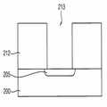
도 5a를 참조하면, 기판(200)의 소정 영역에 제1 불순물들을 도핑하여 불순물 영역(205)을 형성한다. 불순물 영역(205)은, 예를 들면, N형과 같은 제1 도전형을 가질 수 있다.Referring to FIG. 5A, an
불순물 영역(205)을 덮으면서 기판(200) 상에 제1 층간 절연막(212)을 형성한다. 제1 층간 절연막(212)은 산화물을화학 기상 증착 공정, 저압 화학 기상 증착 공정, 플라즈마 증대 화학 기상 증착 공정 또는 고밀도 플라즈마 화학 기상 증착 공정으로 증착하여 형성할 수 있다. 본 발명의 실시예들에 있어서, 기판(200) 상에 하부 구조물이 형성될 경우, 제1 층간 절연막(212)은 상기 하부 구조물을 충분히 덮을 수 있는 높이로 형성된다.The first
제1 층간 절연막(212) 상에 포토레지스트 패턴(도시되지 않음)을 형성한 다음, 상기 포토레지스트 패턴을 식각 마스크로 이용하여 제1 층간 절연막(212)을 부분적으로 식각함으로써, 불순물 영역(205)을 부분적으로 노출시키는 제1 개구(213)를 형성한다. 제1 층간 절연막(212)에 제1 개구(213)를 형성한 다음, 상기 포토레 지스트 패턴을 애싱 공정 및/또는 스트리핑 공정을 이용하여 제거할 수 있다.After forming a photoresist pattern (not shown) on the first
도 5b를 참조하면, 제1 개구(213)에 의해 노출된 불순물 영역(205)을 시드로 이용하는 선택적 에피택시얼 성장 공정을 수행하여, 제1 개구(213)를 채우면서 제1 층간 절연막(212) 상에 실리콘막(도시되지 않음)을 형성한다. 상기 실리콘막은 제1 개구9213)를 충분히 매립하면서 제1 층간 절연막(212)의 상면 상으로 소정의 높이를 가질 수 있다.Referring to FIG. 5B, a first epitaxial insulating
상기 실리콘막의 상부를 제거하여 제1 개구(213) 내의 불순물 영역(205) 상에 실리콘막 패턴(242)을 형성한다. 예를 들면, 실리콘막 패턴(242)은 에치-백 공정을 이용하여 형성될 수 있다. 이 경우, 실리콘막 패턴(242)은 제1 층간 절연막(212)과 실질적으로 동일한 높이를 가질 수 있다.An upper portion of the silicon layer is removed to form a
도 5c를 참조하면, 실리콘막 패턴(242)의 상부 및 하부에 각기 불순물들을 주입하여 상부 도전막 패턴(246) 및 하부 도전막 패턴(248)을 포함하는 도전성 구조물(245)을 형성한다. 예를 들면, 제2 불순물들을 고농도로 실리콘막 패턴(242)의 상부에 주입하여 상부 도전막 패턴(246)을 형성하고, 제3 불순물들을 저농도로 실리콘막 패턴(242)의 하부에 주입하여 하부 도전막 패턴(248)을 형성할 수 있다. 상부 도전막 패턴(246)은 불순물 영역(205)과 동일한 제2 도전형을 가질 수 있으며, 하부 도전막 패턴(248)은 불순물 영역과 상이한 제3 도전형을 가질 수 있다.Referring to FIG. 5C, impurities are implanted into upper and lower portions of the
도전성 구조물(245) 상에 오믹층(249)을 형성한다. 오믹층(249)은 텅스텐 실리사이드, 티타늄 실리사이드, 탄탈륨 실리사이드, 알루미늄 실리사이드, 코발트 실리사이드 등을 사용하여 형성될 수 있다. 본 발명의 실시예들에 따르면, 오믹 층(249)은 금속막을 원자층 적층 공정, 화학 기상 증착 공정, 스퍼터링 공정 또는 싸이클릭 화학 기상 증착 공정을 이행하여 도전성 구조물(245) 상에 형성하고, 상기 금속막에 대해 실리사이데이션 공정을 수행하여 형성될 수 있다. 이 후, 제1 층간 절연막(212) 상에 잔류하는 상기 금속막은 스트리핑 공정 및/또는 애싱 공정으로 제거될 수 있다.An
오믹층(249) 및 제1 층간 절연막(212) 상에 제2 층간 절연막(222)을 형성한다. 제2 층간 절연막(222)은 질화물 또는 산질화물 등의 제1 층간 절연막(212)에 대해 식각 선택비를 갖는 물질을 사용하여 형성할 수 있다. 한편, 제2 층간 절연막(222)은 제1 층간 절연막(212)과 실질적으로 동일한 물질을 사용하여 형성될 수도 있다. 본 발명의 다른 실시예들에 따르면, 제2 층간 절연막(222) 상에 희생막을 추가적으로 형성할 수 있다.A second
제2 층간 절연막(222)을 사진 식각 공정을 통해 부분적으로 식각하여 오믹층(249)을 노출시키는 제2 개구(217)를 형성한 다음, 도 4d 내지 도 4g를 참조하여 설명한 공정들과 실질적으로 동일한 공정들을 수행하여 기판(200) 상에 도 2 또는 도 3을 참조하여 설명한 상변화 메모리 유닛과 실질적으로 동일한 구조를 갖는 상변화 메모리 유닛을 형성한다.The second
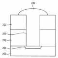
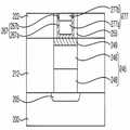
도 13은 본 발명의 실시예들에 따른 전극 구조체를 설명하기 위한 단면도이다.13 is a cross-sectional view for describing an electrode structure according to example embodiments.
도 13을 참조하면, 상기 전극 구조체는 트렌치(769), 리세스 또는 그루브를 갖는 전극(765) 및 충진 구조물(777)을 구비한다.Referring to FIG. 13, the electrode structure includes a
전극(765)은 중공형의 실린더 형상, 중공형의 다각 기둥 형상 또는 컵의 형상을 가질 수 있다. 전극(765)은 금속, 금속 질화물 혹은 금속 실리콘 질화물로 이루어질수 있다. 예를 들면, 전극(765)은 텅스텐, 알루미늄, 구리, 탄탈륨, 티타늄, 몰리브덴, 니오븀, 지르코늄, 알루미늄 질화물, 티타늄 알루미늄 질화물, 티타늄 질화물, 텅스텐 질화물, 탄탈륨 질화물, 몰리브덴 질화물, 몰리브덴 티타늄 질화물, 몰리브덴 알루미늄 질화물, 니오븀 질화물, 티타늄 보론 질화물, 텅스텐 보론 질화물, 지르코늄 알루미늄 질화물, 탄탈륨 또는 탄탈륨 알루미늄 질화물 지르코늄 실리콘 질화물, 탄탈륨 실리콘 질화물, 몰리브덴 실리콘 질화물, 텅스텐 실리콘 질화물, 티타늄 실리콘 질화물 등을 포함할 수 있다. 본 발명의 다른 실시예들에 따르면, 전극(765)은 적어도 하나의 금속막, 적어도 하나의 금속 질화막 및/또는 적어도 하나의 금속실리콘 질화막을 포함하는 복합막 구조를 가질 수 있다.The
충진 구조물(777)은 전극(765)의 트렌치(769) 또는 리세스를 채우면서 전극(765) 상에 형성된다. 충진 구조물(777)은 제1 충진 부재(777a) 및 제2 충진 부재(777b)를 포함한다.
제1 충진 부재(777a)는 전극(765)의 트렌치(769)를 부분적으로 매립한다. 제1 충진 부재(777a)는 도전성 물질 또는 절연성 물질을 포함할 수 있다. 본 발명의 실시예들에 따르면, 제1 충진 부재(777a)는 실리콘을 포함할 수 있다. 예를 들면, 제1 충진 부재(777a)는 폴리실리콘, 아몰퍼스 실리콘, 단결정 실리콘, 불순물이 도핑된 폴리실리콘, 불순물이 도핑된 아몰퍼스 실리콘, 불순물이 도핑된 단결정 실리콘 등을 포함할 수 있다.The
제2 충진 부재(777b)는 제1 충진 부재(777a) 상에 형성된다. 제2 충진 부재(777b) 전극(765)의 트렌치(769)를 충분히 매립한다. 제2 충진 부재(777b)는 절연성 물질을 포함할 수 있다. 예를 들면, 제2 충진 부재(777b)는 실리콘 질화물 등의 질화물이나 실리콘 산화물과 같은 산화물을 포함할 수 있다.The
본 발명의 실시예들에 따르면, 제1 충진 부재(777a) 상에 절연 물질을 포함하는 제2 충진 부재(777b)가 형성되기 때문에, 제1 충진 부재(777a)가 도전성 물질을 포함하더라도 충진 구조물(777)을 통해전류가 흐르지 않는다. 이에 따라, 전극(765) 상에 상변화 물질층이 형성되는 경우, 상기 상변화 물질층과 전극(765) 사이의 접촉 면적이 감소하기 때문에 상대적으로 작은 전류로도 상기 상변화 물질층을 효과적으로 가열할 수 있다.According to embodiments of the present invention, since the
도 14는 본 발명의 다른 실시예들에 따른 전극 구조체를 설명하기 위한 단면도이다.14 is a cross-sectional view for describing an electrode structure according to example embodiments.
도 14를 참조하면, 상기 전극 구조체는 제1 및 제2 충진 부재(777a, 777b)를 포함하는 충진구조물(777)과 제1 및 제2 전극막 패턴(767a, 767b)을 포함하는 전극(767)을 구비한다.Referring to FIG. 14, the electrode structure includes a filling
전극(767)에는 리세스 또는 트렌치가 형성되며, 제1 및 제2 충진 부재(777a, 777b)는 상기 리세스나 트렌치를 채운다. 예를 들면, 제1 충진 부재(777a)는 상기 리세스의 하부를 채울 수 있으며, 제2 충진 부재(777b)는 상기 리세스의 상부를 채울 수 있다. 충진 구조물(777)은 도 13을 참조하여 설명한 충진 구조물(777)과 실질적으로 동일한 구조를 가진다.A recess or a trench is formed in the
제2 전극막 패턴(767b)은 제1 전극막 패턴(767a) 상에 형성된다. 제1 전극막 패턴(767a)은 충진 구조물(777)의 하부를 감싸며, 제2 전극막 패턴(767b)은 충진 구조물(777)의 상부를 감싼다. 제2 전극막 패턴(767b)은 제1 전극막 패턴(767a)에 비해 높은 비저항을 가질 수 있다. 제1 전극막 패턴(767a)은 금속, 금속 질화물 혹은 금속 실리콘 질화물을 포함하며, 제2 전극막 패턴(767b)은 금속 질화물, 금속 실리콘 질화물 또는 도전성 금속 산화물을 포함할 수 있다. 예를 들어, 제2 전극막 패턴(767b)은 티타늄 알루미늄 질화물, 알루미늄 질화물, 티타늄 질화물, 텅스텐 질화물, 탄탈륨 질화물, 몰리브덴 질화물, 니오븀 질화물, 티타늄 실리콘 질화물, 티타늄 보론 질화물, 지르코늄 실리콘 질화물, 텅스텐 실리콘 질화물, 텅스텐 보론 질화물, 지르코늄 알루미늄 질화물, 몰리브덴 실리콘 질화물, 몰리브덴 알루미늄 질화물, 몰리브덴 티타늄 질화물, 탄탈륨 실리콘 질화물 또는 탄탈륨 알루미늄 질화물 등을 포함할 수 있다.The second
도 14에 도시한 바에 따르면, 제2 전극막 패턴(777b)의 두께가 제2 충진 부재(777b)의 두께 보다얇지만, 2 전극막 패턴(777b)의 두께가 제2 충진 부재(777b)의 두께와 실질적으로 동일하거나 혹은 더 두꺼울 수도 있다.As shown in FIG. 14, the thickness of the second
본 발명의 실시예들에 따르면, 상기 전극 구조체는 제1 전극막 패턴(767a)에 비해 상대적으로 높은 비저항을 갖는 제2 전극막 패턴(767b)을 구비하기 때문에, 제1 전극막 패턴(767a)에 전류가 인가될 경우에 제2 전극막 패턴(767b) 및 충진 구조물(777) 상에 접촉되는 상변화 물질층을 보다 효율적으로 가열할 수 있다.According to the exemplary embodiments of the present invention, since the electrode structure includes a second
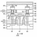
도 6은 본 발명의 실시예들에 따른 상변화 메모리 장치를 설명하기 위한 단 면도이다. 도 6에 도시된 상변화 메모리 장치는 도 2를 참조하여 설명한 상변화 메모리 유닛과 실질적으로 동일하거나 유사한 구조를 갖는 상변화 메모리 유닛을 구비한다. 도 6에 있어서, 실질적으로 서로 직교하는 제1 및 제2 방향은 설명의 편의를 위하여 임의적으로 설정된 것이다.6 is a diagram for describing a phase change memory device according to example embodiments. The phase change memory device shown in FIG. 6 includes a phase change memory unit having a structure substantially the same as or similar to that of the phase change memory unit described with reference to FIG. 2. In FIG. 6, first and second directions substantially perpendicular to each other are arbitrarily set for convenience of description.
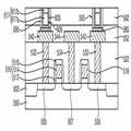
도 6을 참조하면, 상기 상변화 메모리 장치는, 기판(300) 상에 형성된 다이오드(345), 상변화 메모리 유닛, 제1 배선(420) 및 제2 배선(450)을 구비한다.Referring to FIG. 6, the phase change memory device includes a
기판(300)은 실리콘 기판, 게르마늄 기판, 실리콘 게르마늄 기판, SOI 기판, GOI 기판 등과 같은 반도체 기판으로 이루어질 수 있다. 기판(300)에는 상기 제1 방향으로 연장되며, 제1 불순물들이 도핑된 불순물 영역(305)이 형성된다. 예를 들면, 불순물 영역(305)은 N형의 제1 도전형을 가질 수 있다.The
다이오드(345)는 제2 불순물들이 고농도로 도핑된 상부 도전막 패턴(346) 및 제3 불순물들이 저농도로 도핑된 하부 도전막 패턴(348)을 포함한다. 본 발명의 실시예들에 따르면, 상기 제2 불순물들은 P형의 제2 도전형을 가질 수 있으며, 상기 제3 불순물들은 N형의 제3 도전형을 가질 수 있다.The
상기 상변화 메모리 유닛은 다이오드(345) 상에 제공되며, 오믹층(349), 하부 전극(365), 스페이서(355), 충진 구조물(377), 상변화 물질층 패턴(380) 및 상부 전극(390)을 구비한다.The phase change memory unit is provided on the
기판(300) 상에는 불순물 영역(305)을 노출시키는 제1 개구를 갖는 제1 층간 절연막(312)이 형성되며, 다이오드(345)와 오믹층(349)은 상기 제1 개구의 하부를 채우면서 불순물 영역(305) 상에 형성된다. 제1 층간 절연막(312)은 실리콘 산화물 등의 산화물로 구성될 수 있다.A first
오믹층(349)은 금속 실리사이드를 포함할 수 있다. 예를들어, 하부 전극(365)이 티타늄, 텅스텐, 탄탈륨, 코발트 등과 같은 금속을 포함할 경우, 오믹층(349)은 티타늄 실리사이드, 텅스텐 실리사이드, 탄탈륨 실리사이드, 코발트 실리사이드 등을 포함할 수 있다.The
제1 층간 절연막(312) 상에는 오믹층(349)을 노출시키는 제2 개구를 갖는 제2 층간 절연막(322)이 형성된다. 제2 층간 절연막(322)은 제1 층간 절연막(312)에 대해 식각 선택비를 갖는 물질을 포함하거나, 제1 층간 절연막(312)과 실질적으로 동일한 물질을 포함할 수 있다. 예를 들면, 제2 층간 절연막(322)은 실리콘 질화물, 실리콘 산질화물, 실리콘 산화물 등을 포함할 수 있다.A second
하부 전극(365)은 상기 제2 개구 내에 위치하며, 하부 전극(365)에는 트렌치(369), 리세스 또는 그루브가 형성된다. 하부 전극(365)은 금속, 금속 질화물 또는 금속 실리콘 질화물을 포함할 수 있다. 또한, 하부전극(365)은 적어도 하나의 금속막, 적어도 하나의 금속 질화막 및/또는 적어도 하나의 금속실리콘 질화막을 포함하는 복합막 구조를 가질 수 있다.The
충진 구조물(377)은 제1 충진 부재(377a) 및 제2 충진 부재(377b)를 포함하며, 트렌치(369)를 매립하면서 하부 전극(365) 상에 형성된다. 제1 충진 부재(377a)는 트렌치(369)의 하부를 매립하며, 실리콘을 포함하는물질로 구성될 수 있다. 제2 충진 부재(377b)는 제1 충진 부재(377a) 상에 형성되며, 트렌치(369)의 상부를 매립한다. 제2 충진 부재(377b)는 실리콘 질화물이나 실리콘 산화물 등의 절연 물질을 포함할 수 있다.The filling
하부 전극(365)과 상기 제2 개구의 측벽 사이에는 질화물이나 산질화물을 포함하는 스페이서(355)가 제공된다. 예를 들면, 스페이서(355)는 실리콘 질화물 또는 실리콘 산질화물을 포함할 수 있다.A
상변화물질층 패턴(380)은 스페이서(355), 하부 전극(365), 충진 구조물(377) 및 제2 층간 절연막(322) 상에는 형성된다. 상변화 물질층 패턴(380)은 칼코겐 화합물을 포함할 수 있다. 예를 들면, 상변화 물질층 패턴(380)은 게르마늄-안티몬-텔루르를 포함하는 GST 화합물로 구성되거나, 탄소, 질소 및/또는 금속이 도핑된 GST 화합물로 이루어질 수 있다.The phase change
상부 전극(390)은 상변화 물질층 패턴(380) 상에 형성되며, 금속 및/또는 금속 질화물을 포함할 수 있다. 본 발명의 실시예들에 있어서, 상부 전극(390)은 상변화 물질층 패턴(380) 상에 순차적으로 형성된 제1 상부 전극막 패턴(도시하지 않음)과 제2 상부 전극막 패턴(도시하지 않음)을 포함할 수 있다. 이 경우, 상기 제1 상부 전극막 패턴은 금속을 포함할 수 있으며, 상기 제2 상부 전극막 패턴은 도전성 금속 질화물을 포함할 수 있다.The
제3 층간 절연막(402)은 제2 층간 절연막(322) 상에 형성되며, 상변화 물질층 패턴(380) 및 상부 전극(390)을 덮는다. 제1 플러그(410)는 제3 층간 절연막(402)을 관통하여 형성된다. 제3 층간 절연막(402)은 BPSG, PSG, USG, SOG, FOX, TEOS, PE-TEOS) 또는 HDP-CVD 산화물과 같은 실리콘 산화물을 포함할 수 있다.The third
상부 전극(390)은 제1 플러그(410)를 통해제1 배선(420)과 전기적으로 연결 될 수 있다. 제1 배선(420)은 상기 제1 방향에 대해 실질적으로 직교하는 제2 방향을 따라 연장될 수 있다. 제1 배선(420) 및 제1 플러그(410)는 금속, 도전성 금속 질화물 또는 불순물로 도핑된 폴리실리콘 등을 포함할 수 있다. 본 발명의 실시예들에 따르면, 제1 배선(420)은 비트 라인을 포함할 수 있다.The
제4 층간 절연막(432)은 제1 배선(420)을 덮으면서 제3 층간 절연막(402) 상에 형성된다. 제4 층간 절연막(432)은 BPSG, PSG, USG, SOG, FOX, TEOS, PE-TEOS) 또는 HDP-CVD 산화물과 같은 실리콘 산화물을 포함할 수 있다.The fourth
제2 배선(450)은 제4 층간 절연막(432) 상에 형성되며, 제2 플러그(440)를 통해 기판(300)의 소정 영역에 전기적으로 연결된다. 제2 플러그(440)은 제1 내지 제4 층간 절연막(312, 322, 402, 440)을 관통하여 기판(300)에 접촉된다. 제2 배선(450)은 상기 제1 방향을 따라 연장될 수 있다. 제2 배선(450) 및 제2 플러그(440)는 불순물로 도핑된 폴리실리콘, 금속 또는 도전성 금속 질화물을 포함할 수 있다. 본 발명의 일 실시예에 따르면, 제2 배선(450)은 워드 라인을 포함한다.The
본 발명의 실시예들에 따르면, 상기 상변화 메모리 장치는 절연 물질뿐만 아니라 도전성 물질을 포함하는 충진 구조물(377)을 구비한다. 즉, 도전성 물질로 제1 충진 부재(377a)를 형성하더라도, 제1 충진 부재(377a) 상에 절연성 제2 충진 부재(377b)를 형성함으로써, 하부 전극(365)이 상변화 물질층 패턴(380)을 가열하는 효율을 증대시켜 상기 상변화 메모리 장치의 리셋 전류를 감소시킬 수 있다. 특히, 제1 충진 부재(377a)로 종래의 실리콘 질화물 대신에 폴리실리콘, 아몰퍼스 실리콘 또는 단결정 실리콘을 사용할 경우, 충진 구조물(377) 형성 시에 오믹층(349)이 받 는 열적 손상을 크게 감소시킬 수 있다.According to embodiments of the present invention, the phase change memory device includes a filling
도 7은 본 발명의 다른 실시예들에 따른 상변화 메모리 장치들을 설명하기 위한 단면도이다. 도 7에 도시된 상변화 메모리 장치는, 하부 전극(367)의 구조를 제외하면 도 6을 참조하여 설명한 상변화 메모리 장치와 실질적으로 동일하거나 유사한 구조를 가진다. 이 경우, 하부 전극(367)은 도 3을 참조하여 설명한 하부 전극(267)과 실질적으로 동일하거나 유사한 구성을 가진다.7 is a cross-sectional view illustrating phase change memory devices in accordance with other example embodiments of the inventive concept. The phase change memory device illustrated in FIG. 7 has a structure substantially the same as or similar to that of the phase change memory device described with reference to FIG. 6 except for the structure of the
도 7을 참조하면, 상기 상변화 메모리 장치는, 기판(300) 상에 형성된 다이오드(345), 상변화 메모리 유닛, 제1 배선(420) 및 제2 배선(450)을 구비한다.Referring to FIG. 7, the phase change memory device includes a
상기 상변화 메모리 유닛은, 트렌치(369) 또는 그루브를 갖는 하부 전극(367), 제1 및 제2 충진 부재들(377a, 377b)을 포함하는충진 구조물(377), 상변화 물질층 패턴(380) 및 상부 전극(390)을 구비한다. 여기서, 스페이서(355) 및 오믹층(349)이 추가적으로 구비될 수 있다.The phase change memory unit may include a filling
하부 전극(367)은 제1 하부 전극막 패턴(367a) 및 제2 하부 전극막 패턴(367b)을 포함한다. 제1 하부 전극막 패턴(367a)은 충진 구조물(377)의 하부를 감싸며, 금속, 금속 질화물 혹은 금속 실리콘 질화물을 포함할 수 있다. 본 발명의 실시예들에 있어서. 제1 하부 전극막 패턴(367a)은 금속막/금속 질화막 혹은 금속막/금속 실리콘 질화막의 복합막 구조를 가질 수도 있다.The
제2 하부 전극막 패턴(367b)은 제1 하부 전극막 패턴(367a) 상에 형성되며, 충진 구조물(377)의 상부 측면과 접한다. 본 발명의 일 실시예에 따르면, 제2 하부 전극막 패턴(367b)은 충진 구조물(377) 상부를 감싸는 형상을 가질 수 있다. 도 7 에는 제2 하부 전극막 패턴(377b)의 두께가 제2 충진 부재(377b)의 두께보다 얇게 도시되어 있으나, 제2 하부 전극막 패턴(377b)은 제2 충진 부재(377b)와 실질적으로 동일하거나 혹은 두꺼운 두께를 가질 수도 있다.The second lower
제2 하부 전극막 패턴(367b)은 제1 하부 전극막 패턴(367a)에 비해 상대적으로 높은 비저항을 가질 수 있다. 제2 하부 전극막 패턴(367b)은 금속질화물, 금속 실리콘 질화물 혹은 도전성 금속 산화물을 포함할 수 있다. 제2 하부 전극막 패턴(367b)은 금속에 비해 상대적으로 비저항이 높은 물질을 포함하므로, 상변화 물질층 패턴(380)을 효율적으로 가열할 수 있으며, 상기 상변화 메모리 장치의 리셋 전류를 감소시킬 수 있다.The second lower
도 8은 본 발명의 또 다른 실시예들에 따른 상변화 메모리 장치들을 설명하기 위한 단면도이다. 도 8에 도시된 상변화 메모리 장치에 포함된 상변화 메모리 유닛은 트랜지스터를 제외하면 도 6을 참조하여 설명한 상변화 메모리 유닛과 실질적으로 동일하거나 유사한 구조를 가진다.8 is a cross-sectional view illustrating phase change memory devices in accordance with some example embodiments of the present invention. The phase change memory unit included in the phase change memory device illustrated in FIG. 8 has a structure substantially the same as or similar to that of the phase change memory unit described with reference to FIG.
도 8을 참조하면, 상기 상변화 메모리 장치는, 게이트 구조물(510)과 제1 및 제2 불순물 영역들(505, 507)을 구비하는 트랜지스터, 상변화 메모리 유닛, 제1 배선(544) 및 제2 배선(660)을 포함한다.Referring to FIG. 8, the phase change memory device may include a transistor including a
게이트 구조물(510)은 기판(500) 상에 형성된다. 기판(500)은 산화물을 포함하는 소자분리막(502)에 의해 액티브 영역 및 필드 영역으로 구분되며, 게이트 구조물(510)은 상기 액티브 영역 상에 위치한다.The
게이트 구조물(510)은 상기 액티브 영역 상에 순차적으로 형성된 게이트 절 연막 패턴(512), 게이트 전극(514) 및 게이트 마스크(516)를 포함한다. 또한, 게이트 구조물(510)은 게이트 스페이서(518)를 추가적으로 포함할 수 있다. 게이트 절연막 패턴(512)은 실리콘 산화물 또는 금속 산화물을 포함할 수 있으며, 게이트 전극(514)은 도핑된 폴리실리콘, 금속 및/또는 금속 실리사이드를 포함할 수 있다. 또한, 게이트 마스크(516) 및 게이트 스페이서(518)는 각기 실리콘 질화물 또는 실리콘 산질화물을 포함할 수 있다.The
게이트 구조물(510)에 인접한 상기 액티브 영역에는 불순물이 도핑된 제1 및 제2 불순물 영역(505, 507)이 형성된다. 예를 들면, 제1 및 제2 불순물 영역(505, 507)은 각기 소스/드레인 영역들에 해당될 수 있다.First and
제1 층간 절연막(522)은 게이트 구조물(510)을 덮으면서 기판(500) 상에 형성된다. 제1 층간 절연막(522)은 실리콘 산화물과 같은 산화물을 포함할 수 있다.The first
제1 층간 절연막(522)에는 제1 및 제2 불순물 영역(505, 507)을 각기 노출시키는 제1 및 제2 개구(525, 527)가 마련된다. 제1 및 제2 플러그(532, 534)는 각기 제1 및 제2 개구(525, 527)를 채우면서 제1 및 제2 불순물 영역(505, 507) 상에 형성된다. 제1 및 제2 플러그(532, 534)는 각기 금속, 금속 질화물 또는 도핑된 폴리실리콘을 포함할 수 있다. 예를 들면, 제1 및 제2 플러그(532, 534)는 각기 텅스텐, 알루미늄, 티타늄, 구리, 탄탈륨, 텅스텐 질화물, 티타늄 질화물, 알루미늄 질화물, 티타늄 알루미늄 질화물, 탄탈륨 질화물, 도핑된 폴리실리콘 등을 포함할 수 있다.The first
제1 플러그(532) 및 제1 층간 절연막(522) 상에는 패드(542)가 위치하며, 제 1 배선(544)은 제2 플러그(534) 및 제1 층간 절연막(522) 상에 형성된다. 제1 배선(544)은 비트 라인 등을 포함할 수 있다. 패드(542)와 제1 배선(544)은 실질적으로 동일한 물질을 포함할 수 있다. 패드(542) 및 제1 배선(544)은 각기 금속, 금속 질화물 또는 도핑된 폴리실리콘을 포함할 수 있다. 예를 들면, 패드(542)와 제1 배선(544)은 각기 텅스텐, 알루미늄, 구리, 탄탈륨, 티타늄, 몰리브덴, 텅스텐 질화물, 알루미늄 질화물, 티타늄 질화물, 탄탈륨 질화물, 몰리브덴 질화물, 니오븀 질화물, 티타늄 실리콘 질화물, 티타늄 알루미늄 질화물, 티타늄 보론 질화물, 지르코늄 실리콘 질화물, 텅스텐 실리콘 질화물, 텅스텐 보론 질화물, 지르코늄 알루미늄 질화물, 몰리브덴 실리콘 질화물, 몰리브덴 알루미늄 질화물, 탄탈륨 실리콘 질화물, 탄탈륨 알루미늄 질화물 또는 도핑된 폴리실리콘 등을 포함할 수 있다.The
패드(542) 및 제1 배선(544)을 커버하는 제2 층간 절연막(552)이 제1 층간 절연막(522) 상에 형성되며, 제2 층간 절연막(552) 상에는 제3 층간 절연막(562)이 형성된다. 제2 층간 절연막(552)은 산화물을 포함할 수 있으며, 제3 층간 절연막(562)은 질화물 또는 산질화물을 포함할 수 있다. 또한, 제3 층간 절연막(562)은 제2 층간 절연막 552)과 실질적으로 동일한 물질을 포함할 수 있다. 제2 및 제3 층간 절연막(552, 562)에는 패드(542)를 노출시키는 제3 개구(565)가 형성된다.A second
제3 개구(565)를 채우면서 패드(542) 상에는 트렌치(609)를 갖는 하부 전극(605) 및 트렌치(609)를 채우는 충진 구조물(617)이 형성된다. 또한, 스페이서(595) 및 오믹층(585)이 제3 개구(565) 내에 형성된다.A
상변화 물질층 패턴(620)은 하부전극(605), 충진 구조물(617), 스페이 서(595) 및 제3 층간 절연막(562) 상에 형성된다. 상변화 물질층 패턴(620)은 칼코겐 화합물을 포함할 수 있다. 상부 전극(630)은 상변화 물질층 패턴(620) 상에 형성된다. 상부 전극(630)은 금속 또는 도전성 금속 질화물 등을 포함할 수 있다.The phase change
제4 층간 절연막(642)은 상변화 물질층 패턴(620) 및 상부 전극(630)을 덮으면서 제3 층간 절연막(562) 상에 형성된다. 제4 층간 절연막(642)은 실리콘 산화물과 같은 산화물을 포함할 수 있다.The fourth
제4 층간 절연막(642)에는 상부 전극(630)을 노출시키는 제4 개구(645)가 형성되며, 제3 플러그(650)는 제4 개구(645)를 채우면서 상부 전극(630) 상에 형성된다. 제3 플러그(650)는 금속, 금속 질화물 또는 도핑된 폴리실리콘을 포함할 수 있다.A
제2 배선(660)은 제3 플러그(650) 및 제4 층간 절연막(642) 상에 위치한다. 제2 배선(660)은 금속, 금속 질화물 또는 도핑된 폴리실리콘을 포함할 수 있다. 제2 배선(660)은 제3 플러그(650)를 통해 상부 전극(630)에 전기적으로 연결된다.The
본 발명의 실시예들에 있어서, 도 6을 참조하여 설명한 상변화 메모리 장치와 마찬가지로, 제1 충진 부재(617a) 상에 절연성 제2 충진 부재(617b)를 형성함으로써, 하부 전극(605)이 상변화 물질층 패턴(620)을 가열하는 효율을 증대시킬 수 있기 때문에, 상기 상변화 메모리 장치의 리셋 전류를 크게 감소시킬 수 있다. 특히, 제1 충진 부재(617a)로서 실리콘 질화물 대신 폴리실리콘, 아몰퍼스 실리콘 또는 단결정 실리콘을 사용하는 경우, 충진 구조물(617)의형성 시에 오믹층(585)이 받는 열적 손상을 현저하게 감소시킬 수 있다.In the exemplary embodiments of the present invention, similar to the phase change memory device described with reference to FIG. 6, the
도 9는 본 발명의 또 다른 실시예들에 따른 상변화 메모리 장치들을 설명하기 위한 단면도이다. 도 9에 도시된 상변화 메모리 장치는, 하부 전극(607)을 제외하면 도 8을 참조하여 설명한 상변화 메모리 장치와 실질적으로 동일한 구조를 가진다. 또한, 하부 전극(607) 은 도 3을 참조하여 설명한 하부 전극(267)과 실질적으로 동일하거나 유사한 구성을 가진다.9 is a cross-sectional view illustrating phase change memory devices in accordance with some example embodiments of the present invention. The phase change memory device shown in FIG. 9 has the same structure as the phase change memory device described with reference to FIG. 8 except for the
도 9를 참조하면, 상기 상변화 메모리 장치는, 게이트 구조물(510)과 제1 및 제2 불순물 영역(505, 507)을 포함하는 트랜지스터, 상변화 메모리 유닛, 제1 배선(544), 그리고 제2 배선(660)을 구비한다.Referring to FIG. 9, the phase change memory device may include a transistor including a
상기 상변화 메모리 유닛은, 트렌치(609) 또는 그루브를 갖는 하부 전극(607), 제1 및 제2 충진 부재들(617a, 617b)을 구비하는 충진 구조물(617), 상변화 물질층 패턴(620) 그리고 상부 전극(630)을 포함한다. 또한, 상기 상변화 메모리 유닛은 스페이서(595) 및 오믹층(585)을 추가적으로 구비할 수 있다.The phase change memory unit may include a filling
하부 전극(607)은 제1 하부 전극막 패턴(607a) 및 제2 하부 전극막 패턴(607b)을 포함한다. 제1 하부 전극막 패턴(607a)은 충진 구조물(617)의 하부를 감싸며, 금속, 금속 질화물 혹은 금속 실리콘 질화물을 포함할 수 있다. 또한, 제1 하부 전극막 패턴(607a)은 금속막/금속 질화막 혹은 금속막/금속 실리콘 질화막의 복합막 구조를 가질 수도 있다. 제2 하부 전극막 패턴(607b)은 제1 하부 전극막 패턴(607a) 상에 형성되며, 충진 구조물(617)의 상부측면과 접한다.The
본 발명의 실시예들에 있어서, 제2 하부 전극막 패턴(607b)은 충진구조물(617) 상부를 감싸는 형상을 가질 수 있다. 도 9에는제2 하부 전극막 패턴(607b) 의 두께가 제2 충진 부재(617b)의 두께보다 작게 도시되어 있으나, 제2 하부 전극막 패턴(607b)은 제2 충진 부재(617b)과 실질적으로 동일하거나 두꺼운 두께를 가질 수도 있다. 제2 하부 전극막 패턴(607b)은 제1 하부 전극막 패턴(607a)에 비해 상대적으로 높은 비저항을 갖는다. 제2 하부 전극막 패턴(607b)은 금속질화물, 금속 실리콘 질화물을 혹은 도전성 금속 산화물을 포함할 수 있다. 제2 하부 전극막 패턴(607b)이 금속에 비해 상대적으로 비저항이 높은 물질을 포함하기 때문에, 상변화 물질층 패턴(620)을 효율적으로 가열하여 상기 상변화 메모리 장치의 리셋 전류를 감소시킬 수 있다.In example embodiments, the second lower
도 10a 내지 도 10h는 본 발명의 실시예들에 따른 상변화 메모리 장치의 제조 방법을 설명하기 위한 단면도들이다. 도 10a 내지 도 10h에 있어서, 도 6 또는 도 7에 도시한 바와 실질적으로 동일한 구조를 가지는 상변화 메모리 장치의 제조 방법을 예시적으로 설명하지만, 도 10a 내지 도 10h에 도시된 방법이 이에 한정되는 것은 아니다. 한편, 상기 상변화 메모리 장치에 포함되는 상변화 메모리 유닛의 제조 공정들은 도 4a 내지 도 4h를 참조하여 설명한 공정들과 실질적으로 동일하다.10A through 10H are cross-sectional views illustrating a method of manufacturing a phase change memory device according to example embodiments. 10A to 10H, a method of manufacturing a phase change memory device having a structure substantially the same as that shown in FIG. 6 or 7 will be described as an example. However, the method illustrated in FIGS. 10A to 10H is limited thereto. It is not. Meanwhile, manufacturing processes of the phase change memory unit included in the phase change memory device are substantially the same as those described with reference to FIGS. 4A to 4H.
도 10a를 참조하면, 기판(300)의 소정 영역에 제1 불순물들을 도핑하여 불순물 영역(305)을 형성한 다음, 불순물 영역(305)을 덮으면서 기판(300) 상에 제1 층간 절연막(312)을 형성한다.Referring to FIG. 10A, an
제1 층간 절연막(312) 상에는 제2 층간 절연막(322)을 형성된다. 이 경우, 제2 층간 절연막(322) 상에 희생막(도시되지 않음)을 추가적으로 형성할 수도 있 다. 제2 층간 절연막(322) 및 제1 층간 절연막(312)을 부분적으로 식각하여, 불순물 영역(305)을 노출시키는 개구 구조(315)를 형성한다. 개구 구조(315)는 제1 및 제2 층간 절연막(312, 322)에 각기 형성된 제1 개구 및 제2 개구를 포함한다. 한편, 제2 층간 절연막(322) 상에 상기 희생막이 추가적으로 형성될 경우, 상기 희생막에는 제3 개구가 형성될 수 있다.The second
도 10b를 참조하면, 개구 구조(315)를 통해 노출되는 기판(300)을 시드로 이용하는 선택적 에피택시얼 성장 공정을 수행하여, 개구 구조(315)를 매립하는 실리콘막(도시되지 않음)을 형성한다.Referring to FIG. 10B, a selective epitaxial growth process using the
상기 실리콘막의 상부를 제거하여, 개구 구조(315)를 부분적으로 매립하는 실리콘막 패턴(도시되지 않음)을 형성한다. 상기 실리콘막 패턴은 개구 구조(315)의 하부를 매립할 수 있다. 즉, 상기 실리콘막 패턴은 제1 층간 절연막(312)의 제1 개구를 채울 수 있다.An upper portion of the silicon film is removed to form a silicon film pattern (not shown) partially filling the
제2 불순물들을 상기 실리콘막 패턴의 상부에 주입하여 상부 도전막 패턴(346)을 형성하는 한편, 제3 불순물들을 상기 실리콘막 패턴의 하부에 주입하여 하부 도전막 패턴(348)을 형성한다. 이에 따라, 개구 구조(315)의 하부를 채우는 다이오드(345)가 형성된다.Second impurity is implanted over the silicon film pattern to form an upper
다이오드(345) 상에는 실리사이데이션 공정을 이용하여 오믹층(349)이 형성된다. 오믹층(349)은 금속 실리사이드를 포함할 수 있다.The
도 10c를 참조하면, 제2 층간 절연막(322) 상에 개구 구조(315)의 상부를 부분적으로 채우면서 절연막(도시되지 않음)을 형성한 다음, 상기 절연막을 이방성 식각 공정을 이용하여 부분적으로 제거하여 개구 구조(315)의 상부 측벽 상에 예비 스페이서(352)를 형성한다.Referring to FIG. 10C, an insulating film (not shown) is formed while partially filling an upper portion of the
오믹층(349), 예비 스페이서(352) 및 제2 층간 절연막(322) 상에 개구 구조(315)의 상부를 부분적으로 매립하는 하부 전극층(360)을 형성한다. 본 발명의 다른 실시예들에 있어서, 오믹층(349) 및 예비 스페이서(352) 상에 적어도 하나의 금속막, 적어도 하나의 금속 질화막 및/또는 적어도 하나의 금속실리콘 질화막을 구비하는 하부 전극층(360)을 형성할 수도 있다.The
개구 구조(315)의 상부를 충분히 채우면서 하부 전극층(360) 상에 충진층(370)을 형성한다. 충진층(370)은 도전성 물질 또는 절연성 물질을 사용하여 형성될 수 있다. 본 발명의 다른 실시예들에 있어서, 하부 전극층(360) 상에 개구 구조(315)의 상부를 채우는 제1 충진막(도시되지 않음) 및 제2 충진막(도시되지 않음)을 형성할 수도 있다. 여기서, 상기 제1 충진막은 도전성 물질이나 절연성 물질을 사용하여 형성할 수 있고, 상기 제2 충진막은 절연성 물질을 사용하여 형성할 수 있다. 상기 제1 및 제2 충진막에 대해 평탄화 공정을 수행할 경우, 질화 공정 및/또는 산화 공정 없이 제1 및 제2 충진 부재(377a, 377b)를 형성할 수도 있다.The
도 10d를 참조하면, 충진층(370), 하부 전극층(360), 예비 스페이서(352)를 제2 층간 절연막(322)이 노출될 때까지 제거한다. 이 때, 제2 층간 절연막(322)의 일부및 예비 스페이서(352)의 일부도 함께 제거될 수 있다. 따라서, 오믹층(349) 상에는 예비 충진 구조물(도시되지 않음), 하부 전극(365) 및 스페이서(355)가 형성된다. 한편, 전술한 바와 같이, 상기 예비 충진 구조물, 하부 전극(365) 및 스페 이서(355)는 2회의 평탄화 공정을 적용하여 형성될 수도 있다.Referring to FIG. 10D, the
상기 예비 충진 구조물에 대해 제1 질화 공정 또는 제1 산화 공정을 수행하여 제2 충진 부재(377b)를 형성한다. 따라서, 하부 전극(365) 상에는 제1 및 제2 충진 부재(377a, 377b)를 포함하는 충진 구조물(377)이 형성된다.The
도 10e를 참조하면, 하부 전극(367)의 상부에 대해 제2 질화 공정을 수행하여 금속 질화물을 포함하는 제2 하부 전극막 패턴(367b)을 형성한다. 이에 따라, 제1 및 제2 하부 전극막 패턴(367a, 367b)을 포함하는 하부 전극(367)이 완성된다. 본 발명의 다른 실시예들에 있어서, 하부 전극(367)의 상부에 대해 제2 산화 공정을 수행하여 도전성 금속 산화물을 포함하는 제2 하부 전극막 패턴(367b)을 형성할 수도 있다.Referring to FIG. 10E, a second nitriding process is performed on the upper portion of the
도 10f를 참조하면, 하부 전극(367), 충진 구조물(377), 스페이서(355) 및 제2 층간 절연막(322) 상에 상변화 물질층 패턴(380)과 상부전극(390)을 형성함으로써, 도 3을 참조하여 설명한 상변화 메모리 유닛과 실질적으로 동일한 구조를 갖는 상변화 메모리 유닛을 형성한다. 한편, 전술한 제2 하부 전극막 패턴(367b)을 형성하는 공정을 생략할 경우에는, 하부 전극(365), 충진 구조물(377), 스페이서(355) 및 제2 층간 절연막(322) 상에 상변화 물질층 패턴(380)과 상부 전극(390)이 형성되기 때문에, 도 2를 참조하여 설명한 상변화 메모리 유닛과 실질적으로 동일한 구조를 갖는 상변화 메모리 유닛을 형성할 수 있다.Referring to FIG. 10F, the phase change
제2 층간 절연막(322) 상에 상변화 물질층 패턴(380)과 상부 전극(390)을 커버하면서 상부 전극(390)을 노출시키는 상부 개구(405)를 갖는 제3 층간 절연 막(402)을 형성한다. 제3 층간 절연막(402)은 실리콘 산화물 등의 산화물을 사용하여 형성될 수 있다.A third
상부 전극(390) 상에 상부 개구(405)를 채우는 제1 플러그(410)를 형성한다. 제1 플러그(410)는 금속, 도전성 금속 질화물 또는 도핑된 폴리실리콘을 화학 기상 증착 공정, 스퍼터링 공정, 원자층 적층 공정, 전자 빔 증착공정 또는 펄스 레이저 증착 공정으로 증착하여 형성할 수 있다.A
도 10g를 참조하면, 제1 플러그(410) 및 제3 층간 절연막(402) 상에 제1 배선(420)을 형성한다. 제1 배선(420)은 금속, 도전성 금속 질화물 또는 도핑된 폴리실리콘을 화학 기상 증착 공정, 스퍼터링 공정, 원자층 적층 공정, 전자 빔 증착 공정 또는 펄스 레이저 증착 공정으로 증착하여 형성할 수 있다.Referring to FIG. 10G, a
제3 층간 절연막(402) 상에 제1 플러그(410)를 커버하면서 기판(300)의 일부를 노출시키는 제3 개구(435)를 갖는 제4 층간 절연막(432)을 형성한다. 제4 층간 절연막 (432)은 산화물을 사용하여 형성될 수 있다.A fourth
도 10h를 참조하면, 기판(300) 상에 제3 개구(435)를 채우는 제2 플러그(440)를 형성한다. 제2 플러그(440)는 금속, 도전성 금속 질화물 또는 도핑된 폴리실리콘을 화학 기상 증착 공정, 스퍼터링 공정, 원자층 적층 공정, 전자 빔 증착 공정 또는 펄스 레이저 증착 공정으로 증착하여 형성할 수 있다.Referring to FIG. 10H, a
제4 층간 절연막(432) 상에 제2 플러그(440)에 접촉되는 제2 배선(450)을 형성한다. 제2 배선(450)은 금속, 도전성 금속 질화물 또는 도핑된 폴리실리콘을 화학 기상 증착 공정, 스퍼터링 공정, 원자층 적층 공정, 전자 빔 증착 공정 또는 펄 스 레이저 증착 공정으로 증착하여 형성할 수 있다. 그 결과, 본 발명의 실시예들에 따른 상변화 메모리 장치가 완성된다.A
본 발명의 실시예들에 따르면, 종래 고온의 증착 공정을 필요로 하는 실리콘 질화물 대신에 상대적으로 낮은 온도에서 증착 가능한 폴리실리콘, 아몰퍼스 실리콘, 단결정 실리콘 등을 사용하여 충진층(370)을 형성함으로써, 충진층(370)의형성 시에 오믹층(349)이 받는 열적 손상을 현저하게 감소시킬 수 있다. 또한, 질화 공정 및/또는 산화 공정을 통해 도전막을 부분적으로 절연막으로 변화시킬수 있다. 더욱이, 하부전극(365)의 상부를 질화 및/또는 산화처리하여 상대적으로 높은 비저항을 갖는 제2 하부 전극막 패턴(367b)을 형성할 수 있기 때문에, 상변화 물질층 패턴(380)을 가열하는 효율을 증대시켜 리셋 전류를 감소시킬 수 있다.According to embodiments of the present invention, instead of silicon nitride, which requires a high temperature deposition process, the
도 11a 내지 도 11c는 본 발명의 다른 실시예들에 따른 상변화 메모리 장치의 제조 방법을 설명하기 위한 단면도들이다. 도 11a 내지 도 11c를 참조하여 설명하는 상변화 메모리 장치의 제조 방법은 도 5a 내지 도 5c를 참조로 설명한 상변화 메모리 유닛의 제조 방법과 실질적으로 동일하거나 유사하다.11A through 11C are cross-sectional views illustrating a method of manufacturing a phase change memory device in accordance with some example embodiments of the present invention. The manufacturing method of the phase change memory device described with reference to FIGS. 11A through 11C is substantially the same as or similar to the manufacturing method of the phase change memory unit described with reference to FIGS. 5A through 5C.
도 11a를 참조하면, 기판(300)의 소정 영역에 제1 불순물들을 도핑하여 불순물 영역(305)을 형성한 후, 불순물 영역(305)을 커버하면서 기판(300) 상에 제1 층간 절연막(312)을 형성한다.Referring to FIG. 11A, after the
제1 층간 절연막(312)을 부분적으로 식각하여 불순물 영역(305)을 노출시키는 제1 개구(313)를 형성한 다음, 제1 개구(313)를 채우면서 불순물 영역(305) 상에 실리콘막(341)을 형성한다.The first
도 11b를 참조하면, 실리콘막(341)의 상부를 제거하여, 불순물 영역(305) 상에 제1 개구(313)의 하부를 매립하는 실리콘막 패턴(도시되지 않음)을 형성한 후, 상기 실리콘막 패턴으로부터 다이오드(345)를 형성한다. 예를 들면, 제2 불순물들을 상기 실리콘막 패턴의 상부에 주입하여 상부 도전막 패턴(346)을 형성하고, 제3 불순물들을 상기 실리콘막 패턴의 하부에 주입하여 하부 도전막 패턴(348)을 형성한다. 이에 따라, 상부 및 하부 도전막 패턴(346, 348)을 포함하는 다이오드(345)가 형성된다.Referring to FIG. 11B, after the upper portion of the
다이오드(345) 상에 금속 실리사이드를 사용하여 오믹층(349)을 형성하여, 제1 개구(313)를 완전히 매립한다.The
도 11c를 참조하면, 오믹층(349) 및 제1 층간 절연막 (312) 상에 제2 층간 절연막(322)을 형성한 후, 제2 층간 절연막(322)을 부분적으로 식각한다. 따라서, 제2 층간 절연막(322)에는 오믹층(349)을 노출시키는 제2 개구(315)가 형성된다. 한편, 제2 층간 절연막(322) 상에 희생막이 추가적으로 형성될 경우에는, 상기 희생막에는 상기 제2 개구와 실질적으로 동일한 폭의 제3 개구가 형성될 수 있다.Referring to FIG. 11C, after the second
이후, 도 10c 내지 도 10h를 참조하여 설명한 공정들과 실질적으로 동일한 공정들을 수행하여 본 발명의 실시예들에 따른 상변화 메모리 장치를 완성한다.Subsequently, the phase change memory device according to the exemplary embodiments of the present invention is completed by performing the same processes as those described with reference to FIGS. 10C to 10H.
도 12a 내지 도 12i는 본 발명의 또 다른 실시예들에 따른 상변화 메모리 장치의 제조 방법을 설명하기 위한 단면도들이다. 도 12a 내지 도 12i에 있어서, 도 8 및 도 9에 도시한 바와 실질적으로 동일한 구조를 갖는 상변화 메모리 장치의 제조 방법을 예시적으로 설명하지만, 도 12a 내지도 12i에 도시된 방법이 이에 한정 되는 것은 아니다. 한편, 상기 상변화 메모리 장치에 포함된 상변화 메모리 유닛을 형성하는 공정들은 도 4a 내지 도 4h를 참조하여 설명한 공정들과 실질적으로 동일하다.12A to 12I are cross-sectional views illustrating a method of manufacturing a phase change memory device according to still other embodiments of the present invention. 12A to 12I, a method of manufacturing a phase change memory device having a structure substantially the same as that shown in FIGS. 8 and 9 will be exemplarily described, but the method shown in FIGS. 12A to 12I is limited thereto. It is not. Meanwhile, the processes of forming the phase change memory unit included in the phase change memory device are substantially the same as those described with reference to FIGS. 4A through 4H.
도 12a를 참조하면, STI 공정 또는 열 산화 공정을 통해 기판(500)에 소자 분리막(502)을 형성하여 기판(500)을 액티브 영역 및 필드영역으로 구분한다.Referring to FIG. 12A, an
기판(500)의 액티브 영역 상에 게이트 절연막, 게이트 도전막 및 게이트 마스크층을 차례로 형성한다. 상기 게이트 절연막은 산화물 또는 금속 산화물을 사용하여 형성될 수 있으며, 상기 게이트 도전막은 불순물이 도핑된 폴리실리콘, 금속 또는 금속 질화물을 사용하여 형성될 수 있다. 상기게이트 마스크층은 상기 게이트 절연막 및 상기 게이트 도전막에 대하여 식각 선택비를 갖는 물질을 사용하여 형성될 수 있다.A gate insulating film, a gate conductive film, and a gate mask layer are sequentially formed on the active region of the
사진 식각 공정을 통해 상기 게이트 마스크층, 상기 게이트 도전막 및 상기 게이트 절연막을 패터닝함으로써, 상기 액티브 영역 상에 게이트 절연막 패턴(512), 게이트 전극(514) 및 게이트 마스크(516)를 형성한다. 이에 따라, 상기 액티브 영역 상에는 게이트 절연막 패턴(512), 게이트 전극(514) 및 게이트 마스크(516)를 포함하는 게이트 구조물(510)이 형성된다. 한편, 게이트 마스크(516)를 덮으면서 기판(500) 상에 절연막을 형성한 다음, 상기 절연막을 부분적으로 식각하여 게이트 절연막 패턴(512), 게이트 전극(514) 및 게이트 마스크(516)의 측벽들 상에 게이트 스페이서(518)를 추가적으로 형성할 수도 있다.The gate mask layer, the gate conductive layer, and the gate insulating layer are patterned through a photolithography process to form a gate insulating
게이트 구조물(510)을 마스크들로 이용하는 이온 주입 공정을 통해 게이트 구조물(510)에 인접한 상기 액티브 영역에 제1 및 제2 불순물 영역(505, 507)을 형성한다. 이에 따라, 게이트 구조물(510)과 제1 및 제2 불순물 영역(505, 507)을 포함하는 트랜지스터가 기판(500)의 액티브 영역 상에 형성된다.First and
도 12b를 참조하면, 상기 트랜지스터들을 커버하는 제1 층간 절연막(522)을 기판(500) 상에 형성한 다음, 제1 층간 절연막(522)을 부분적으로 식각하여 제1 및 제2 불순물 영역(505, 507)을 노출시키는 제1 및 제2 개구(525, 527)를 형성한다.Referring to FIG. 12B, a first
제1 및 제2 개구(525, 527)를 채우면서 제1 층간 절연막(522) 상에 제1 도전막을 형성한 후, 제1 층간 절연막(522)의 상면이 노출될 때까지 상기 제1 도전막을 제거하여 제1 및 제2 불순물 영역(505, 507) 상에 제1 및 제2 개구(525, 527)를 채우는 제1 및 제2 플러그(532, 534)를 형성한다.After forming the first conductive film on the first
제1 및 제2 플러그(532, 534)와 제1 층간 절연막(522) 상에 금속, 도전성 금속 질화물, 도핑된 폴리실리콘 등을 사용하여 제2 도전막을 형성한 다음, 상기 제2 도전막을 부분적으로제거함으로써, 제1 및 제2 플러그(532, 534) 상에 각기 패드(542) 및 제1 배선(544)을 형성한다. 제1 배선(544)은 비트 라인으로 이용될 수 있다.A second conductive film is formed on the first and
도 12c를 참조하면, 제1 층간 절연막(522) 상에 패드(542) 및 제1 배선(544)을 덮으면서 제2 층간 절연막(552)을 형성한 다음, 제2 층간 절연막(550) 상에 제3 층간 절연막(562)을 형성한다.12C, a second
제3 층간 절연막(562) 상에 포토레지스트 패턴(도시되지 않음)을 형성한 다음, 상기 포토레지스트 패턴을 식각 마스크로 이용하여 제3 층간 절연막(562) 및 제2 층간 절연막(552)을 부분적으로 식각함으로써, 패드(542)를 노출시키는 제3 개구(555)를 형성한다. 상기 포토레지스트 패턴은 애싱 공정 및/또는 스트리핑 공정을 이용하여 제3 층간 절연막(562)으로부터 제거될 수 있다.After forming a photoresist pattern (not shown) on the third
도 12d를 참조하면, 제3 개구(555)를 통해 노출된 패드(542) 상에 오믹층(585)을 형성한 후, 제3 개구(555)를 부분적으로 매립하는 절연막(도시되지 않음)을 오믹층(349) 및 제3 층간 절연막(562) 상에 형성한다.Referring to FIG. 12D, after forming the
상기 절연막을 이방성 식각 공정을 사용하여 식각하여 제3 개구(555)의 측벽 상에 제1 예비 스페이서(592)를 형성한 다음, 오믹층(585), 제1 예비 스페이서(592) 및 제3 층간 절연막(562) 상에 제3 개구(555)를 부분적으로 채우는 하부 전극층(600)을 형성한다. 도시하지는 않았으나, 오믹층(585) 및 제1 예비 스페이서(592) 상에 금속막/금속 질화막 혹은 금속막/금속 실리콘 질화막의 복합막을 갖는 하부 전극층(600)을 형성할 수도 있다.The insulating layer is etched using an anisotropic etching process to form first
도 12e를 참조하면, 제3 개구(555)를 충분하게 채우면서 하부 전극층(600) 상에 충진층(도시되지 않음)을 형성한다. 상기 충진층은 도전성 물질 혹은 절연성 물질을 사용하여 형성될 수 있다. 이와는 달리, 제3 개구(555)를 완전히 채우도록 하부 전극층(600) 상에 제1 충진막(도시되지 않음) 및 제2 충진막(도시되지 않음)을 형성할 수도 있다. 이 때, 상기 제1 충진막은 도전성 혹은 절연성 물질을 사용하여 형성할 수 있고, 상기 제2 충진막은 절연성 물질을 사용하여 형성할 수 있다. 여기서, 상기 제1 및 제2 충진막에 대해 평탄화 공정을 수행하여, 질화 공정 및/또는 산화 공정을 거치지 않고 제1 및 제2 충진 부재(617a, 617b)를 형성할 수도 있 다.Referring to FIG. 12E, a filling layer (not shown) is formed on the
상기 충진층, 하부 전극층(600) 및 제1 예비 스페이서(592)의 상부를 기계적 화학적 연마 공정 및/또는 에치-백 공정을 이용하여 제거함으로써, 각기 충진층 패턴(612), 하부 전극층 패턴(602) 및 제2 예비 스페이서(594)를 형성한다.The
도 12f를 참조하면, 충진층 패턴(612), 하부 전극층 패턴(602) 및 제2 예비 스페이서(594)를 재차 기계적 화학적 연마 공정 및/또는 에치-백 공정으로 제3 층간 절연막(562)이 노출될 때까지 제거함으로써, 예비 충진 구조물(도시되지 않음), 하부 전극(605) 및 스페이서(595)를 형성한다.Referring to FIG. 12F, the third
상기 예비 충진 구조물의 상부에 대해 제1 질화 공정 및/또는 제1 산화공정을 수행하여 제2 충진 부재(617b)를 형성한다. 이에 따라, 상기 예비 충진 구조물로부터 제1 및 제2 충진 부재(617a, 617b)을 포함하는 충진 구조물(617)이 형성된다.A first nitriding process and / or a first oxidation process may be performed on the upper portion of the preliminary filling structure to form a second filling member 617b. Accordingly, a filling
도 12g를 참조하면, 하부 전극(605)의 상부에 대해 제2 질화 공정 및/또는 제2 산화 공정을 수행하여 제2 하부 전극막 패턴(607b)을 형성한다. 따라서, 오믹층(585) 상에 제1 및 제2 하부 전극막 패턴(607a, 607b)을 포함하는 하부 전극(607)이 형성된다.Referring to FIG. 12G, the second lower
도 12h를 참조하면, 하부 전극(607), 충진 구조물(617), 스페이서(595) 및 제3 층간 절연막(562) 상에 상변화 물질층 패턴(620)과 상부 전극(630)을 형성하여, 도 9에 도시된 바와 실질적으로 동일한 구조를 갖는 상변화 메모리 유닛을 완성한다. 한편, 전술한 제2 하부 전극막 패턴(607b)을 형성하는 공정을 생략할 경우 에는, 하부 전극(605), 충진 구조물(617), 스페이서(595) 및 제3 층간 절연막(562) 상에 상변화 물질층 패턴(620)과 상부 전극(630)이 형성되어, 도 8에 도시된 바와 실질적으로 동일한 구조를 갖는 상변화 메모리 유닛이 형성된다.Referring to FIG. 12H, the phase change
제3 층간 절연막(562) 상에는 상변화 물질층 패턴(620)과 상부 전극(630)을 커버하면서, 상부 전극(630)을 노출시키는 제4 개구(645)를 갖는 제4 층간 절연막(642)이 형성된다.On the third
도 12i를 참조하면, 상부 전극(630) 상에 제4 개구(645)를 채우는 제3 플러그(650)를 형성한 후, 제3 플러그(650) 및 제4 층간 절연막(642) 상에 제2 배선(660)을 형성하여 상변화 메모리 장치를 완성한다.Referring to FIG. 12I, after forming the
본 발명의 실시예들에 따르면, 상변화 메모리 유닛은 절연성 물질뿐만 아니라 도전성 물질로 이루어진 충진 구조물을 포함할 수 있다. 즉, 도전성 물질로 제1 충진 부재를 형성하더라도, 상기 제1 충진 부재 상에 절연성 제2 충진 부재가 형성됨으로써, 상변화 물질층 패턴을 가열하는 효율을 증대시킬 수 있다. 이에 따라, 상기 상변화 메모리 유닛의 리셋 전류를 감소시킬 수 있다. 특히, 상기 제1 충진 부재로서 종래의 실리콘 질화물 대신에 폴리실리콘, 아몰퍼스 실리콘 또는 단결정 실리콘을 사용하는 경우, 상기 충진 구조물의 형성 시에 오믹층이 받는 열적 손상을 현저하게 감소시킬 수 있다. 또한, 하부 전극에 대해 질화 공정 및/또는 산화공정을 수행하여 하부 전극의 비저항을 증가시킬 수 있다. 결국, 상기상변화 물질층 패턴을 가열하는 효율을 향상시켜 리셋 전류를 더욱 감소시킬 수 있다.According to embodiments of the present invention, the phase change memory unit may include a filling structure made of a conductive material as well as an insulating material. That is, even when the first filling member is formed of the conductive material, the insulating second filling member is formed on the first filling member, thereby increasing the efficiency of heating the phase change material layer pattern. Accordingly, the reset current of the phase change memory unit can be reduced. In particular, when polysilicon, amorphous silicon, or single crystal silicon is used instead of the conventional silicon nitride as the first filling member, it is possible to significantly reduce the thermal damage to the ohmic layer when the filling structure is formed. In addition, the specific resistance of the lower electrode may be increased by performing a nitriding process and / or an oxidation process on the lower electrode. As a result, the reset current may be further reduced by improving the efficiency of heating the phase change material layer pattern.
상술한 바와 같이, 본 발명의 실시예들을 참조하여 설명하였지만 해당 기술 분야에서 통상의 지식을 가진 자라면 하기의 특허청구범위에 기재된 본 발명의 사상 및 영역으로부터 벗어나지 않는 범위 내에서 본 발명을 다양하게 수정 및 변경시킬 수 있음을 이해할 수 있을 것이다.As described above, the present invention has been described with reference to the embodiments of the present invention, but those skilled in the art may vary the present invention without departing from the spirit and scope of the present invention as set forth in the claims below. It will be appreciated that modifications and variations can be made.
Claims (32)
Translated fromKoreanPriority Applications (3)
| Application Number | Priority Date | Filing Date | Title |
|---|---|---|---|
| KR1020070060442AKR100881055B1 (en) | 2007-06-20 | 2007-06-20 | Phase change memory unit, manufacturing method thereof, phase change memory device including same and manufacturing method thereof |
| US11/775,657US7863173B2 (en) | 2007-06-20 | 2007-07-10 | Variable resistance non-volatile memory cells and methods of fabricating same |
| JP2008160959AJP2009004785A (en) | 2007-06-20 | 2008-06-19 | Nonvolatile memory cell with variable resistance and method for manufacturing the same |
Applications Claiming Priority (1)
| Application Number | Priority Date | Filing Date | Title |
|---|---|---|---|
| KR1020070060442AKR100881055B1 (en) | 2007-06-20 | 2007-06-20 | Phase change memory unit, manufacturing method thereof, phase change memory device including same and manufacturing method thereof |
Publications (2)
| Publication Number | Publication Date |
|---|---|
| KR20080111903A KR20080111903A (en) | 2008-12-24 |
| KR100881055B1true KR100881055B1 (en) | 2009-01-30 |
Family
ID=40135517
Family Applications (1)
| Application Number | Title | Priority Date | Filing Date |
|---|---|---|---|
| KR1020070060442AActiveKR100881055B1 (en) | 2007-06-20 | 2007-06-20 | Phase change memory unit, manufacturing method thereof, phase change memory device including same and manufacturing method thereof |
Country Status (3)
| Country | Link |
|---|---|
| US (1) | US7863173B2 (en) |
| JP (1) | JP2009004785A (en) |
| KR (1) | KR100881055B1 (en) |
Cited By (3)
| Publication number | Priority date | Publication date | Assignee | Title |
|---|---|---|---|---|
| US8138490B2 (en) | 2007-06-18 | 2012-03-20 | Samsung Electronics Co., Ltd. | Variable resistance non-volatile memory cells and methods of fabricating same |
| US8237149B2 (en) | 2007-06-18 | 2012-08-07 | Samsung Electronics Co., Ltd. | Non-volatile memory device having bottom electrode |
| US8501623B2 (en) | 2009-07-22 | 2013-08-06 | Samsung Electronics Co., Ltd. | Method of forming a semiconductor device having a metal silicide and alloy layers as electrode |
Families Citing this family (34)
| Publication number | Priority date | Publication date | Assignee | Title |
|---|---|---|---|---|
| US7776688B2 (en)* | 2007-08-08 | 2010-08-17 | Spansion Llc | Use of a polymer spacer and Si trench in a bitline junction of a flash memory cell to improve TPD characteristics |
| US7906392B2 (en)* | 2008-01-15 | 2011-03-15 | Sandisk 3D Llc | Pillar devices and methods of making thereof |
| KR100971423B1 (en)* | 2008-04-04 | 2010-07-21 | 주식회사 하이닉스반도체 | Phase change memory device and manufacturing method thereof |
| IT1391864B1 (en)* | 2008-09-30 | 2012-01-27 | St Microelectronics Rousset | RESISTIVE MEMORY CELL AND METHOD FOR THE MANUFACTURE OF A RESISTIVE MEMORY CELL |
| KR101019987B1 (en)* | 2008-10-20 | 2011-03-09 | 주식회사 하이닉스반도체 | Diode Formation Method of Phase Change Memory Device |
| KR20100066117A (en)* | 2008-12-09 | 2010-06-17 | 삼성전자주식회사 | Semoconductor device and method of thereof |
| KR20100076274A (en)* | 2008-12-26 | 2010-07-06 | 주식회사 하이닉스반도체 | Phase changeable memory device and method of manufacturing the same |
| KR101127236B1 (en)* | 2008-12-29 | 2012-03-29 | 주식회사 하이닉스반도체 | Method for fabricating resistance memory device |
| KR20100084215A (en)* | 2009-01-16 | 2010-07-26 | 삼성전자주식회사 | Phase change memory device having barrier protective layer silicicd bottom electrode and method for manufacturing same |
| US8084760B2 (en)* | 2009-04-20 | 2011-12-27 | Macronix International Co., Ltd. | Ring-shaped electrode and manufacturing method for same |
| US8575753B2 (en)* | 2009-05-27 | 2013-11-05 | Samsung Electronics Co., Ltd. | Semiconductor device having a conductive structure including oxide and non oxide portions |
| JP5775288B2 (en)* | 2009-11-17 | 2015-09-09 | 三星電子株式会社Samsung Electronics Co.,Ltd. | Semiconductor device |
| KR20110076394A (en)* | 2009-12-29 | 2011-07-06 | 삼성전자주식회사 | Phase change memory device |
| JP2011199035A (en)* | 2010-03-19 | 2011-10-06 | Toshiba Corp | Semiconductor memory device |
| KR101709323B1 (en)* | 2010-04-23 | 2017-02-22 | 삼성전자주식회사 | Resistance variable memory device and method for forming the same |
| JP5696378B2 (en)* | 2010-06-15 | 2015-04-08 | ソニー株式会社 | Manufacturing method of storage device |
| JP5580126B2 (en)* | 2010-07-14 | 2014-08-27 | 株式会社東芝 | Nonvolatile memory device and manufacturing method thereof |
| KR101124341B1 (en)* | 2011-01-07 | 2012-03-16 | 주식회사 하이닉스반도체 | Phase change random access memory and method for fabricating the same |
| JP2013021108A (en)* | 2011-07-11 | 2013-01-31 | Toshiba Corp | Semiconductor memory device and method of manufacturing the same |
| CN103000515B (en)* | 2011-09-14 | 2015-07-08 | 中芯国际集成电路制造(北京)有限公司 | Semiconductor device and manufacturing method thereof |
| KR20130046664A (en)* | 2011-10-28 | 2013-05-08 | 삼성전자주식회사 | Methods of forming a pattern and methods of manufacturing a semiconductor device using the same |
| KR101907972B1 (en)* | 2011-10-31 | 2018-10-17 | 주식회사 원익아이피에스 | Apparatus and Method for treating substrate |
| US9269747B2 (en) | 2012-08-23 | 2016-02-23 | Micron Technology, Inc. | Self-aligned interconnection for integrated circuits |
| US9129894B2 (en)* | 2012-09-17 | 2015-09-08 | Intermolecular, Inc. | Embedded nonvolatile memory elements having resistive switching characteristics |
| US9184308B1 (en)* | 2012-09-20 | 2015-11-10 | Univerity of South Florida | Devices having nanoscale structures and methods for making same |
| US9111857B2 (en) | 2012-09-21 | 2015-08-18 | Micron Technology, Inc. | Method, system and device for recessed contact in memory array |
| US9385316B2 (en)* | 2014-01-07 | 2016-07-05 | Taiwan Semiconductor Manufacturing Co., Ltd. | RRAM retention by depositing Ti capping layer before HK HfO |
| US10003022B2 (en) | 2014-03-04 | 2018-06-19 | Taiwan Semiconductor Manufacturing Co., Ltd. | RRAM cell structure with conductive etch-stop layer |
| KR102143438B1 (en)* | 2014-12-04 | 2020-08-11 | 삼성전자주식회사 | Active structure of semiconductor device and method of forming the same |
| US10134984B1 (en)* | 2014-12-31 | 2018-11-20 | Crossbar, Inc. | Two-terminal memory electrode comprising a non-continuous contact surface |
| US9461245B1 (en)* | 2015-11-13 | 2016-10-04 | Taiwan Semiconductor Manufacturing Co., Ltd. | Bottom electrode for RRAM structure |
| KR102552896B1 (en)* | 2016-08-02 | 2023-07-07 | 삼성전자주식회사 | Magnetoresistive random access device and method of manufacturing the same |
| TWI699914B (en)* | 2016-09-08 | 2020-07-21 | 聯華電子股份有限公司 | Semiconductor device and the method of making the same |
| US10276791B1 (en) | 2017-11-09 | 2019-04-30 | Taiwan Semiconductor Manufacturing Co., Ltd. | Resistive random access memory device |
Citations (4)
| Publication number | Priority date | Publication date | Assignee | Title |
|---|---|---|---|---|
| KR20030081900A (en)* | 2002-04-15 | 2003-10-22 | 삼성전자주식회사 | Method of fabricating Phase change Memory device |
| KR20050084240A (en)* | 2002-12-13 | 2005-08-26 | 오보닉스, 아이엔씨. | Forming phase change memories |
| KR20060002133A (en)* | 2004-07-01 | 2006-01-09 | 주식회사 하이닉스반도체 | Manufacturing method of phase change memory device |
| KR20060065919A (en)* | 2004-12-10 | 2006-06-14 | 주식회사 하이닉스반도체 | Phase change memory device and its manufacturing method |
Family Cites Families (101)
| Publication number | Priority date | Publication date | Assignee | Title |
|---|---|---|---|---|
| JPS4840307B1 (en)* | 1970-06-12 | 1973-11-29 | ||
| US4571513A (en)* | 1982-06-21 | 1986-02-18 | Eaton Corporation | Lateral bidirectional dual notch shielded FET |
| JPS6379373A (en)* | 1986-09-24 | 1988-04-09 | Hitachi Ltd | Semiconductor device and its manufacturing method |
| US5751012A (en)* | 1995-06-07 | 1998-05-12 | Micron Technology, Inc. | Polysilicon pillar diode for use in a non-volatile memory cell |
| US5831276A (en)* | 1995-06-07 | 1998-11-03 | Micron Technology, Inc. | Three-dimensional container diode for use with multi-state material in a non-volatile memory cell |
| JP3097561B2 (en)* | 1995-07-26 | 2000-10-10 | ヤマハ株式会社 | Field emission cathode and method of manufacturing field emission device |
| KR970054343A (en)* | 1995-12-20 | 1997-07-31 | 이준 | Silicon / silicon germanium dipole transistor manufacturing method |
| US6750091B1 (en)* | 1996-03-01 | 2004-06-15 | Micron Technology | Diode formation method |
| US5952671A (en)* | 1997-05-09 | 1999-09-14 | Micron Technology, Inc. | Small electrode for a chalcogenide switching device and method for fabricating same |
| KR100385946B1 (en)* | 1999-12-08 | 2003-06-02 | 삼성전자주식회사 | Method for forming a metal layer by an atomic layer deposition and a semiconductor device with the metal layer as a barrier metal layer, an upper electrode, or a lower electrode of capacitor |
| US6617192B1 (en) | 1997-10-01 | 2003-09-09 | Ovonyx, Inc. | Electrically programmable memory element with multi-regioned contact |
| US5939788A (en)* | 1998-03-11 | 1999-08-17 | Micron Technology, Inc. | Copper diffusion barrier, aluminum wetting layer and improved methods for filling openings in silicon substrates with cooper |
| US6921962B1 (en)* | 1998-12-18 | 2005-07-26 | Texas Instruments Incorporated | Integrated circuit having a thin film resistor located within a multilevel dielectric between an upper and lower metal interconnect layer |
| US7338908B1 (en)* | 2003-10-20 | 2008-03-04 | Novellus Systems, Inc. | Method for fabrication of semiconductor interconnect structure with reduced capacitance, leakage current, and improved breakdown voltage |
| WO2000039842A1 (en)* | 1998-12-23 | 2000-07-06 | Infineon Technologies Ag | Capacitor electrode structure |
| US6235571B1 (en)* | 1999-03-31 | 2001-05-22 | Micron Technology, Inc. | Uniform dielectric layer and method to form same |
| US7247876B2 (en)* | 2000-06-30 | 2007-07-24 | Intel Corporation | Three dimensional programmable device and method for fabricating the same |
| US6376353B1 (en)* | 2000-07-03 | 2002-04-23 | Chartered Semiconductor Manufacturing Ltd. | Aluminum and copper bimetallic bond pad scheme for copper damascene interconnects |
| US6440837B1 (en)* | 2000-07-14 | 2002-08-27 | Micron Technology, Inc. | Method of forming a contact structure in a semiconductor device |
| JP2002043315A (en)* | 2000-07-26 | 2002-02-08 | Sony Corp | Semiconductor device and manufacturing method thereof |
| US6455424B1 (en)* | 2000-08-07 | 2002-09-24 | Micron Technology, Inc. | Selective cap layers over recessed polysilicon plugs |
| US6339544B1 (en)* | 2000-09-29 | 2002-01-15 | Intel Corporation | Method to enhance performance of thermal resistor device |
| US6563164B2 (en)* | 2000-09-29 | 2003-05-13 | Ovonyx, Inc. | Compositionally modified resistive electrode |
| JP4644924B2 (en)* | 2000-10-12 | 2011-03-09 | ソニー株式会社 | Semiconductor device and manufacturing method thereof |
| US6555858B1 (en)* | 2000-11-15 | 2003-04-29 | Motorola, Inc. | Self-aligned magnetic clad write line and its method of formation |
| US6649928B2 (en) | 2000-12-13 | 2003-11-18 | Intel Corporation | Method to selectively remove one side of a conductive bottom electrode of a phase-change memory cell and structure obtained thereby |
| US20020074658A1 (en)* | 2000-12-20 | 2002-06-20 | Chien Chiang | High-resistivity metal in a phase-change memory cell |
| US6569705B2 (en)* | 2000-12-21 | 2003-05-27 | Intel Corporation | Metal structure for a phase-change memory device |
| US6646297B2 (en)* | 2000-12-26 | 2003-11-11 | Ovonyx, Inc. | Lower electrode isolation in a double-wide trench |
| US6534781B2 (en)* | 2000-12-26 | 2003-03-18 | Ovonyx, Inc. | Phase-change memory bipolar array utilizing a single shallow trench isolation for creating an individual active area region for two memory array elements and one bipolar base contact |
| US6531373B2 (en)* | 2000-12-27 | 2003-03-11 | Ovonyx, Inc. | Method of forming a phase-change memory cell using silicon on insulator low electrode in charcogenide elements |
| US6818481B2 (en)* | 2001-03-07 | 2004-11-16 | Micron Technology, Inc. | Method to manufacture a buried electrode PCRAM cell |
| KR100408742B1 (en)* | 2001-05-10 | 2003-12-11 | 삼성전자주식회사 | Capacitor in integrated circuits device and method therefor |
| US7102150B2 (en)* | 2001-05-11 | 2006-09-05 | Harshfield Steven T | PCRAM memory cell and method of making same |
| US6642102B2 (en)* | 2001-06-30 | 2003-11-04 | Intel Corporation | Barrier material encapsulation of programmable material |
| US6511867B2 (en) | 2001-06-30 | 2003-01-28 | Ovonyx, Inc. | Utilizing atomic layer deposition for programmable device |
| US6881623B2 (en)* | 2001-08-29 | 2005-04-19 | Micron Technology, Inc. | Method of forming chalcogenide comprising devices, method of forming a programmable memory cell of memory circuitry, and a chalcogenide comprising device |
| US6764894B2 (en)* | 2001-08-31 | 2004-07-20 | Ovonyx, Inc. | Elevated pore phase-change memory |
| US6507061B1 (en)* | 2001-08-31 | 2003-01-14 | Intel Corporation | Multiple layer phase-change memory |
| US6884689B2 (en)* | 2001-09-04 | 2005-04-26 | United Microelectronics Corp. | Fabrication of self-aligned bipolar transistor |
| JP3749847B2 (en)* | 2001-09-27 | 2006-03-01 | 株式会社東芝 | Phase change nonvolatile memory device and drive circuit thereof |
| US6992365B2 (en)* | 2001-10-12 | 2006-01-31 | Ovonyx, Inc. | Reducing leakage currents in memories with phase-change material |
| US6624485B2 (en)* | 2001-11-05 | 2003-09-23 | Matrix Semiconductor, Inc. | Three-dimensional, mask-programmed read only memory |
| US6815818B2 (en)* | 2001-11-19 | 2004-11-09 | Micron Technology, Inc. | Electrode structure for use in an integrated circuit |
| DE60220245D1 (en) | 2002-01-17 | 2007-07-05 | St Microelectronics Srl | Integrated resistance element, phase change Storage element with such resistance element, and method for its production |
| US7087919B2 (en)* | 2002-02-20 | 2006-08-08 | Micron Technology, Inc. | Layered resistance variable memory device and method of fabrication |
| US6838691B2 (en)* | 2002-03-04 | 2005-01-04 | Macronix International, Co., Ltd. | Chalcogenide memory and method of manufacturing the same |
| AU2003233406A1 (en)* | 2002-03-15 | 2003-09-29 | Axon Technologies Corporation | Programmable structure, an array including the structure, and methods of forming the same |
| US6864500B2 (en)* | 2002-04-10 | 2005-03-08 | Micron Technology, Inc. | Programmable conductor memory cell structure |
| US6855975B2 (en)* | 2002-04-10 | 2005-02-15 | Micron Technology, Inc. | Thin film diode integrated with chalcogenide memory cell |
| KR100449949B1 (en)* | 2002-04-26 | 2004-09-30 | 주식회사 하이닉스반도체 | Method for fabricating capacitor in ferroelectric memory device |
| US20030227091A1 (en)* | 2002-06-06 | 2003-12-11 | Nishant Sinha | Plating metal caps on conductive interconnect for wirebonding |
| US6856002B2 (en)* | 2002-08-29 | 2005-02-15 | Micron Technology, Inc. | Graded GexSe100-x concentration in PCRAM |
| KR100481865B1 (en)* | 2002-11-01 | 2005-04-11 | 삼성전자주식회사 | Phase changeable memory device and method of fabricating the same |
| KR100481866B1 (en)* | 2002-11-01 | 2005-04-11 | 삼성전자주식회사 | Phase changeable memory device and method of fabricating the same |
| US7314776B2 (en)* | 2002-12-13 | 2008-01-01 | Ovonyx, Inc. | Method to manufacture a phase change memory |
| US7049623B2 (en)* | 2002-12-13 | 2006-05-23 | Ovonyx, Inc. | Vertical elevated pore phase change memory |
| US7060619B2 (en)* | 2003-03-04 | 2006-06-13 | Infineon Technologies Ag | Reduction of the shear stress in copper via's in organic interlayer dielectric material |
| US7022579B2 (en)* | 2003-03-14 | 2006-04-04 | Micron Technology, Inc. | Method for filling via with metal |
| TWI245288B (en)* | 2003-03-20 | 2005-12-11 | Sony Corp | Semiconductor memory element and semiconductor memory device using the same |
| US7459715B2 (en)* | 2003-04-03 | 2008-12-02 | Kabushiki Kaisha Toshiba | Resistance change memory device |
| US6893959B2 (en)* | 2003-05-05 | 2005-05-17 | Infineon Technologies Ag | Method to form selective cap layers on metal features with narrow spaces |
| KR100979710B1 (en)* | 2003-05-23 | 2010-09-02 | 삼성전자주식회사 | Semiconductor memory device and manufacturing method |
| US7067865B2 (en)* | 2003-06-06 | 2006-06-27 | Macronix International Co., Ltd. | High density chalcogenide memory cells |
| KR100504701B1 (en)* | 2003-06-11 | 2005-08-02 | 삼성전자주식회사 | Phase change memory device and method for forming the same |
| US7381611B2 (en)* | 2003-08-04 | 2008-06-03 | Intel Corporation | Multilayered phase change memory |
| US6815704B1 (en)* | 2003-09-04 | 2004-11-09 | Silicon Storage Technology, Inc. | Phase change memory device employing thermally insulating voids |
| US20050124155A1 (en)* | 2003-12-03 | 2005-06-09 | Brooks Joseph F. | Electrode structures and method to form electrode structures that minimize electrode work function variation |
| US7030651B2 (en)* | 2003-12-04 | 2006-04-18 | Viciciv Technology | Programmable structured arrays |
| US6937507B2 (en)* | 2003-12-05 | 2005-08-30 | Silicon Storage Technology, Inc. | Memory device and method of operating same |
| US7057923B2 (en)* | 2003-12-10 | 2006-06-06 | International Buisness Machines Corp. | Field emission phase change diode memory |
| KR100546406B1 (en)* | 2004-04-10 | 2006-01-26 | 삼성전자주식회사 | Phase change memory device manufacturing method |
| DE102004031135A1 (en)* | 2004-06-28 | 2006-01-19 | Infineon Technologies Ag | Resistive semiconductor element based on a solid-state ion conductor |
| KR100626381B1 (en)* | 2004-07-19 | 2006-09-20 | 삼성전자주식회사 | Phase change memory device and its formation method |
| KR100629265B1 (en) | 2004-08-04 | 2006-09-29 | 삼성전자주식회사 | A method of forming a conductive layer having a local high resistance region and a semiconductor device manufactured using the same |
| KR100655796B1 (en) | 2004-08-17 | 2006-12-11 | 삼성전자주식회사 | Phase change memory device and manufacturing method thereof |
| US7135696B2 (en)* | 2004-09-24 | 2006-11-14 | Intel Corporation | Phase change memory with damascene memory element |
| KR100626388B1 (en)* | 2004-10-19 | 2006-09-20 | 삼성전자주식회사 | Phase change memory device and forming method thereof |
| US7238959B2 (en)* | 2004-11-01 | 2007-07-03 | Silicon Storage Technology, Inc. | Phase change memory device employing thermally insulating voids and sloped trench, and a method of making same |
| US7189626B2 (en)* | 2004-11-03 | 2007-03-13 | Micron Technology, Inc. | Electroless plating of metal caps for chalcogenide-based memory devices |
| US7396759B1 (en)* | 2004-11-03 | 2008-07-08 | Novellus Systems, Inc. | Protection of Cu damascene interconnects by formation of a self-aligned buffer layer |
| KR100687709B1 (en)* | 2004-11-04 | 2007-02-27 | 한국전자통신연구원 | Multi-bit type phase change memory device and its driving method |
| US7220983B2 (en)* | 2004-12-09 | 2007-05-22 | Macronix International Co., Ltd. | Self-aligned small contact phase-change memory method and device |
| KR100612913B1 (en)* | 2004-12-16 | 2006-08-16 | 한국과학기술연구원 | Phase change memory with AIEN heat release layer and TiN electrode |
| US7326951B2 (en)* | 2004-12-16 | 2008-02-05 | Macronix International Co., Ltd. | Chalcogenide random access memory |
| US7214958B2 (en)* | 2005-02-10 | 2007-05-08 | Infineon Technologies Ag | Phase change memory cell with high read margin at low power operation |
| US7348590B2 (en)* | 2005-02-10 | 2008-03-25 | Infineon Technologies Ag | Phase change memory cell with high read margin at low power operation |
| KR100675279B1 (en)* | 2005-04-20 | 2007-01-26 | 삼성전자주식회사 | Phase Shift Memory Adopting Cell Diodes and Their Manufacturing Methods |
| US7312114B2 (en)* | 2005-04-27 | 2007-12-25 | Infineon Technologies Ag | Manufacturing method for a trench capacitor having an isolation collar electrically connected with a substrate on a single side via a buried contact for use in a semiconductor memory cell |
| KR100689831B1 (en)* | 2005-06-20 | 2007-03-08 | 삼성전자주식회사 | Phase change memory cells having a cell diode and a lower electrode self-aligned with each other and methods of manufacturing the same |
| KR100642645B1 (en)* | 2005-07-01 | 2006-11-10 | 삼성전자주식회사 | Memory device having a highly integrated cell structure and manufacturing method thereof |
| US7274034B2 (en)* | 2005-08-01 | 2007-09-25 | Micron Technology, Inc. | Resistance variable memory device with sputtered metal-chalcogenide region and method of fabrication |
| KR100655440B1 (en)* | 2005-08-30 | 2006-12-08 | 삼성전자주식회사 | Phase change memory device and its formation method |
| US7279411B2 (en)* | 2005-11-15 | 2007-10-09 | International Business Machines Corporation | Process for forming a redundant structure |
| US7394088B2 (en)* | 2005-11-15 | 2008-07-01 | Macronix International Co., Ltd. | Thermally contained/insulated phase change memory device and method (combined) |
| US7449710B2 (en)* | 2005-11-21 | 2008-11-11 | Macronix International Co., Ltd. | Vacuum jacket for phase change memory element |
| JP4396621B2 (en)* | 2005-12-02 | 2010-01-13 | ソニー株式会社 | Storage element and storage device |
| JP4691454B2 (en)* | 2006-02-25 | 2011-06-01 | エルピーダメモリ株式会社 | Phase change memory device and manufacturing method thereof |
| US7499355B2 (en)* | 2006-07-31 | 2009-03-03 | Sandisk 3D Llc | High bandwidth one time field-programmable memory |
| TW200810092A (en)* | 2006-08-15 | 2008-02-16 | Ind Tech Res Inst | Phase-change memory and fabrication method thereof |
| US7473986B2 (en)* | 2006-09-22 | 2009-01-06 | Taiwan Semiconductor Manufacturing Co., Ltd. | Positive-intrinsic-negative (PIN) diode semiconductor devices and fabrication methods thereof |
- 2007
- 2007-06-20KRKR1020070060442Apatent/KR100881055B1/enactiveActive
- 2007-07-10USUS11/775,657patent/US7863173B2/enactiveActive
- 2008
- 2008-06-19JPJP2008160959Apatent/JP2009004785A/enactivePending
Patent Citations (4)
| Publication number | Priority date | Publication date | Assignee | Title |
|---|---|---|---|---|
| KR20030081900A (en)* | 2002-04-15 | 2003-10-22 | 삼성전자주식회사 | Method of fabricating Phase change Memory device |
| KR20050084240A (en)* | 2002-12-13 | 2005-08-26 | 오보닉스, 아이엔씨. | Forming phase change memories |
| KR20060002133A (en)* | 2004-07-01 | 2006-01-09 | 주식회사 하이닉스반도체 | Manufacturing method of phase change memory device |
| KR20060065919A (en)* | 2004-12-10 | 2006-06-14 | 주식회사 하이닉스반도체 | Phase change memory device and its manufacturing method |
Cited By (3)
| Publication number | Priority date | Publication date | Assignee | Title |
|---|---|---|---|---|
| US8138490B2 (en) | 2007-06-18 | 2012-03-20 | Samsung Electronics Co., Ltd. | Variable resistance non-volatile memory cells and methods of fabricating same |
| US8237149B2 (en) | 2007-06-18 | 2012-08-07 | Samsung Electronics Co., Ltd. | Non-volatile memory device having bottom electrode |
| US8501623B2 (en) | 2009-07-22 | 2013-08-06 | Samsung Electronics Co., Ltd. | Method of forming a semiconductor device having a metal silicide and alloy layers as electrode |
Also Published As
| Publication number | Publication date |
|---|---|
| JP2009004785A (en) | 2009-01-08 |
| US7863173B2 (en) | 2011-01-04 |
| US20080315174A1 (en) | 2008-12-25 |
| KR20080111903A (en) | 2008-12-24 |
Similar Documents
| Publication | Publication Date | Title |
|---|---|---|
| KR100881055B1 (en) | Phase change memory unit, manufacturing method thereof, phase change memory device including same and manufacturing method thereof | |
| KR100911473B1 (en) | Phase change memory unit, manufacturing method thereof, phase change memory device including same and manufacturing method thereof | |
| KR100782496B1 (en) | Method for manufacturing semiconductor device having self-aligned cell diode and method for manufacturing phase change memory device using same | |
| KR100873890B1 (en) | Phase-change memory unit, method of forming the phase-change memory unit, phase-change memory device having the phase-change memory unit and method of manufacturing the phase-change memory device | |
| US7419881B2 (en) | Phase changeable memory device and method of formation thereof | |
| KR100827661B1 (en) | Phase change memory device having a double bottom electrode and method of manufacturing the same | |
| US8575753B2 (en) | Semiconductor device having a conductive structure including oxide and non oxide portions | |
| KR100766504B1 (en) | Semiconductor device and manufacturing method thereof | |
| KR100714900B1 (en) | Semiconductor device having a buried gate electrode and a manufacturing method thereof | |
| US7804703B2 (en) | Phase change memory device having Schottky diode and method of fabricating the same | |
| KR101872949B1 (en) | Phase change memory device and method of manufacturing the same | |
| KR101823500B1 (en) | Method of manufacturing a phase change memory device | |
| US20050110983A1 (en) | Phase change memory devices with contact surface area to a phase changeable material defined by a sidewall of an electrode hole and methods of forming the same | |
| US20090250679A1 (en) | Phase-change memory device and method of fabricating the same | |
| KR20130135603A (en) | Phase change memory devices and methods of manufacturing the same | |
| US7897959B2 (en) | Phase change memory device having a word line contact | |
| KR20150127367A (en) | Method of filling an opening and method of manufacturing a phase-change memory device using the same | |
| KR20130110406A (en) | Phase-change memory devices and methods of manufacturing the same | |
| KR100629265B1 (en) | A method of forming a conductive layer having a local high resistance region and a semiconductor device manufactured using the same | |
| KR20100077535A (en) | Contact structure, method of manufacturing the same, phase changeable memory device having the same and method of manufacturing the phase changeable memory device | |
| KR101298258B1 (en) | Method of manufacturing phase-change memory device | |
| US20100243981A1 (en) | Phase-change random access memory device | |
| KR20090108479A (en) | Method for forming phase change memory unit, method for manufacturing phase change memory device using same, and phase change memory device formed accordingly | |
| KR20090021762A (en) | Manufacturing Method of Phase Change Memory Device | |
| KR20080002490A (en) | Phase change memory device and manufacturing method thereof |
Legal Events
| Date | Code | Title | Description |
|---|---|---|---|
| A201 | Request for examination | ||
| PA0109 | Patent application | Patent event code:PA01091R01D Comment text:Patent Application Patent event date:20070620 | |
| PA0201 | Request for examination | ||
| E902 | Notification of reason for refusal | ||
| PE0902 | Notice of grounds for rejection | Comment text:Notification of reason for refusal Patent event date:20080326 Patent event code:PE09021S01D | |
| E701 | Decision to grant or registration of patent right | ||
| PE0701 | Decision of registration | Patent event code:PE07011S01D Comment text:Decision to Grant Registration Patent event date:20081022 | |
| PG1501 | Laying open of application | ||
| GRNT | Written decision to grant | ||
| PR0701 | Registration of establishment | Comment text:Registration of Establishment Patent event date:20090122 Patent event code:PR07011E01D | |
| PR1002 | Payment of registration fee | Payment date:20090122 End annual number:3 Start annual number:1 | |
| PG1601 | Publication of registration | ||
| PR1001 | Payment of annual fee | Payment date:20111229 Start annual number:4 End annual number:4 | |
| FPAY | Annual fee payment | Payment date:20130102 Year of fee payment:5 | |
| PR1001 | Payment of annual fee | Payment date:20130102 Start annual number:5 End annual number:5 | |
| FPAY | Annual fee payment | Payment date:20140103 Year of fee payment:6 | |
| PR1001 | Payment of annual fee | Payment date:20140103 Start annual number:6 End annual number:6 | |
| FPAY | Annual fee payment | Payment date:20141231 Year of fee payment:7 | |
| PR1001 | Payment of annual fee | Payment date:20141231 Start annual number:7 End annual number:7 | |
| FPAY | Annual fee payment | Payment date:20160104 Year of fee payment:8 | |
| PR1001 | Payment of annual fee | Payment date:20160104 Start annual number:8 End annual number:8 | |
| FPAY | Annual fee payment | Payment date:20170102 Year of fee payment:9 | |
| PR1001 | Payment of annual fee | Payment date:20170102 Start annual number:9 End annual number:9 | |
| FPAY | Annual fee payment | Payment date:20191226 Year of fee payment:12 | |
| PR1001 | Payment of annual fee | Payment date:20191226 Start annual number:12 End annual number:12 | |
| PR1001 | Payment of annual fee | Payment date:20201230 Start annual number:13 End annual number:13 | |
| PR1001 | Payment of annual fee | Payment date:20211229 Start annual number:14 End annual number:14 | |
| PR1001 | Payment of annual fee | Payment date:20221221 Start annual number:15 End annual number:15 | |
| PR1001 | Payment of annual fee | Payment date:20231226 Start annual number:16 End annual number:16 |