KR100879476B1 - Organic light emitting device - Google Patents
Organic light emitting deviceDownload PDFInfo
- Publication number
- KR100879476B1 KR100879476B1KR1020070098380AKR20070098380AKR100879476B1KR 100879476 B1KR100879476 B1KR 100879476B1KR 1020070098380 AKR1020070098380 AKR 1020070098380AKR 20070098380 AKR20070098380 AKR 20070098380AKR 100879476 B1KR100879476 B1KR 100879476B1
- Authority
- KR
- South Korea
- Prior art keywords
- injection layer
- light emitting
- hole injection
- layer
- compound
- Prior art date
- Legal status (The legal status is an assumption and is not a legal conclusion. Google has not performed a legal analysis and makes no representation as to the accuracy of the status listed.)
- Active
Links
Images


Classifications
- H—ELECTRICITY
- H05—ELECTRIC TECHNIQUES NOT OTHERWISE PROVIDED FOR
- H05B—ELECTRIC HEATING; ELECTRIC LIGHT SOURCES NOT OTHERWISE PROVIDED FOR; CIRCUIT ARRANGEMENTS FOR ELECTRIC LIGHT SOURCES, IN GENERAL
- H05B33/00—Electroluminescent light sources
- H05B33/12—Light sources with substantially two-dimensional radiating surfaces
- H05B33/20—Light sources with substantially two-dimensional radiating surfaces characterised by the chemical or physical composition or the arrangement of the material in which the electroluminescent material is embedded
- H—ELECTRICITY
- H10—SEMICONDUCTOR DEVICES; ELECTRIC SOLID-STATE DEVICES NOT OTHERWISE PROVIDED FOR
- H10K—ORGANIC ELECTRIC SOLID-STATE DEVICES
- H10K50/00—Organic light-emitting devices
- H10K50/10—OLEDs or polymer light-emitting diodes [PLED]
- H10K50/14—Carrier transporting layers
- H10K50/15—Hole transporting layers
- H10K50/155—Hole transporting layers comprising dopants
- H—ELECTRICITY
- H10—SEMICONDUCTOR DEVICES; ELECTRIC SOLID-STATE DEVICES NOT OTHERWISE PROVIDED FOR
- H10K—ORGANIC ELECTRIC SOLID-STATE DEVICES
- H10K50/00—Organic light-emitting devices
- H10K50/10—OLEDs or polymer light-emitting diodes [PLED]
- H10K50/17—Carrier injection layers
- H—ELECTRICITY
- H10—SEMICONDUCTOR DEVICES; ELECTRIC SOLID-STATE DEVICES NOT OTHERWISE PROVIDED FOR
- H10K—ORGANIC ELECTRIC SOLID-STATE DEVICES
- H10K50/00—Organic light-emitting devices
- H10K50/10—OLEDs or polymer light-emitting diodes [PLED]
- H10K50/14—Carrier transporting layers
- H10K50/16—Electron transporting layers
- H10K50/165—Electron transporting layers comprising dopants
- H—ELECTRICITY
- H10—SEMICONDUCTOR DEVICES; ELECTRIC SOLID-STATE DEVICES NOT OTHERWISE PROVIDED FOR
- H10K—ORGANIC ELECTRIC SOLID-STATE DEVICES
- H10K85/00—Organic materials used in the body or electrodes of devices covered by this subclass
- H10K85/30—Coordination compounds
- H10K85/321—Metal complexes comprising a group IIIA element, e.g. Tris (8-hydroxyquinoline) gallium [Gaq3]
- H10K85/324—Metal complexes comprising a group IIIA element, e.g. Tris (8-hydroxyquinoline) gallium [Gaq3] comprising aluminium, e.g. Alq3
- H—ELECTRICITY
- H10—SEMICONDUCTOR DEVICES; ELECTRIC SOLID-STATE DEVICES NOT OTHERWISE PROVIDED FOR
- H10K—ORGANIC ELECTRIC SOLID-STATE DEVICES
- H10K85/00—Organic materials used in the body or electrodes of devices covered by this subclass
- H10K85/60—Organic compounds having low molecular weight
- H—ELECTRICITY
- H10—SEMICONDUCTOR DEVICES; ELECTRIC SOLID-STATE DEVICES NOT OTHERWISE PROVIDED FOR
- H10K—ORGANIC ELECTRIC SOLID-STATE DEVICES
- H10K85/00—Organic materials used in the body or electrodes of devices covered by this subclass
- H10K85/60—Organic compounds having low molecular weight
- H10K85/649—Aromatic compounds comprising a hetero atom
- H10K85/654—Aromatic compounds comprising a hetero atom comprising only nitrogen as heteroatom
Landscapes
- Physics & Mathematics (AREA)
- Optics & Photonics (AREA)
- Electroluminescent Light Sources (AREA)
Abstract
Translated fromKoreanDescription
Translated fromKorean본 발명은 유기 발광 소자에 관한 것으로서, 보다 상세하게는 발광 효율, 수명 등의 특성이 개선된 유기 발광 소자에 관한 것이다.The present invention relates to an organic light emitting device, and more particularly, to an organic light emitting device having improved characteristics such as luminous efficiency and lifetime.
본 발명은 고품위 유기 발광 소자 개발을 위한 필수 선행 기술에 관한 것으로, 유기 발광 소자의 소비 전력 절감 및 수명 개선에 관한 것이다.The present invention relates to the essential prior art for the development of high quality organic light emitting device, and relates to the reduction of power consumption and lifespan of the organic light emitting device.
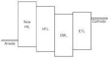
유기 발광 소자라 함은 도 1에서 보여지는 바와 같이 두 전극 사이에 삽입되어 있는 유기막에 전류를 인가시, 유기막에서 전자와 정공의 결합에 의하여 빛이 발생하는 장치를 말한다. 따라서 유기 발광 소자는 고화질, 빠른 응답 속도 및 광시야각의 특성을 갖는 경량 박형의 정보 표시 장치 구현을 가능하게 하는 장점을 갖는다. 이는 유기 발광 표시 소자 기술의 급격한 성장을 선도하는 원동력이 되었고, 현재 유기 발광 소자는 모바일 폰 뿐 아니라 기타 고품위의 정보 표시 장치에까지 그 응용 영역이 확장되고 있다. As shown in FIG. 1, an organic light emitting diode refers to a device in which light is generated by a combination of electrons and holes in an organic film when a current is applied to an organic film inserted between two electrodes. Therefore, the organic light emitting diode has an advantage of enabling a lightweight, thin information display device having high quality, fast response speed, and wide viewing angle. This has been a driving force for the rapid growth of the organic light emitting display technology, and the application area of the organic light emitting device is expanding not only to mobile phones but also to other high quality information display devices.
이러한 유기 발광 소자의 급성장은 학술적 측면 뿐 아니라, 산업 기술 측면에서 TFT-LCD와 같은 기타 정보 표시 소자와의 경쟁이 불가피하게 되었고, 기존의 유기 발광 소자는 양적, 질적 성장을 저해하는 가장 큰 요인으로 남아 있는 소자의 효율, 수명 향상 및 소비 전력 절감이라는 기술적 한계를 극복해야 하는 난국에 직면해 있다.The rapid growth of the organic light emitting device is inevitably competing with other information display devices such as TFT-LCD in terms of industrial technology as well as the academic aspect, and the existing organic light emitting device is the biggest factor that inhibits quantitative and qualitative growth. The technical challenges of remaining efficiency, longer life and lower power consumption are faced with the challenge.
상기 종래 기술의 문제점을 해결하기 위하여 본 발명이 이루고자 하는 기술적 과제는 우수한 전기적 특성을 갖는 적색, 녹색, 청색, 흰색 등의 모든 칼라의 형광 및 인광 소자에 적합한 정공주입층 재료를 포함하는 유기막을 채용한 고효율, 저전압, 고휘도, 장수명의 유기 발광 소자를 제공하는 것이다.The technical problem to be achieved by the present invention to solve the problems of the prior art employs an organic film containing a hole injection layer material suitable for fluorescent and phosphorescent devices of all colors, such as red, green, blue, white, etc. having excellent electrical properties It is to provide an organic light emitting device having high efficiency, low voltage, high brightness and long life.
상기 기술적 과제를 이루기 위하여, 본 발명에서는 제1 전극; 제2 전극; 상기 제1 전극과 상기 제2 전극 사이에 위치한 발광층 및 상기 제1 전극과 상기 제2 전극 사이에 위치한 정공주입층을 포함하는 유기 발광 소자로서, 상기 정공주입층은, Mo, Li, Na, K, Rb, Cs, Be, Mg, Ca, Sr, Ba 및 B로 이루어진 군으로부터 선택된 원소 및 O, F, S, Cl, Se, Br 및 I로 이루어진 군으로부터 선택된 원소로 이루어진 제1 화합물 및 정공주입층 형성용 유기 화합물인 제2 화합물을 포함하는 것을 특징으로 하는 유기 발광 소자를 제공한다.In order to achieve the above technical problem, in the present invention a first electrode; Second electrode; An organic light emitting device comprising a light emitting layer positioned between the first electrode and the second electrode and a hole injection layer positioned between the first electrode and the second electrode, wherein the hole injection layer is formed of Mo, Li, Na, K And a first compound and a hole injection comprising an element selected from the group consisting of Rb, Cs, Be, Mg, Ca, Sr, Ba and B and an element selected from the group consisting of O, F, S, Cl, Se, Br and I It provides an organic light emitting device comprising a second compound which is an organic compound for forming a layer.
바람직하게는, 상기 제1 화합물 및 상기 제2 화합물의 혼합비가 1 : 1 내지 3 : 1이다.Preferably, the mixing ratio of the first compound and the second compound is from 1: 1 to 3: 1.
또한 바람직하게는, 상기 제1 화합물 및 제2 화합물을 포함하는 정공주입층 이외에 또 다른 정공주입층을 더 포함할 수 있다.Also preferably, in addition to the hole injection layer including the first compound and the second compound, another hole injection layer may be further included.
바람직하게는, 상기 제1 화합물 및 제2 화합물을 포함하는 정공주입층과 상기 제2 정공주입층의 두께의 비가 1 : 99 내지 1 : 9이다.Preferably, the ratio of the thickness of the hole injection layer containing the first compound and the second compound and the second hole injection layer is 1:99 to 1: 9.
본 발명에서의 정공주입층 재료는 우수한 전기적 특성을 가지며, 적색, 녹색, 청색, 흰색 등의 모든 칼라의 형광 및 인광 소자에 적합한 정공 주입 재료로서, 이를 이용하여 고효율, 저전압, 고휘도, 장수명의 유기 발광 소자를 제작할 수 있다.The hole injection layer material according to the present invention has excellent electrical properties, and is a hole injection material suitable for fluorescent and phosphorescent devices of all colors such as red, green, blue, white, etc. A light emitting element can be manufactured.
이하, 본 발명을 보다 상세하게 설명하기로 한다.Hereinafter, the present invention will be described in more detail.
본 발명은 제1 전극; 제2 전극; 상기 제1 전극과 상기 제2 전극 사이에 위치한 발광층; 및 상기 제1 전극과 상기 제2 전극 사이에 위치한 정공주입층을 포함하는 유기 발광 소자로서, 상기 정공주입층은 제1 화합물 및 제2 화합물을 포함하는데, 제1 화합물은, Mo, Li, Na, K, Rb, Cs, Be, Mg, Ca, Sr, Ba 및 B로 이루어진 군으로부터 선택된 원소와 O, F, S, Cl, Se, Br 및 I로 이루어진 군으로부터 선택된 원소로 이루어지고, 제2 화합물은 통상적으로 사용될 수 있는 정공주입층 형성용 유기 화합물이다.The present invention is a first electrode; Second electrode; A light emitting layer positioned between the first electrode and the second electrode; And a hole injection layer positioned between the first electrode and the second electrode, wherein the hole injection layer includes a first compound and a second compound, wherein the first compound is Mo, Li, Na , K, Rb, Cs, Be, Mg, Ca, Sr, Ba and B and an element selected from the group consisting of O, F, S, Cl, Se, Br and I, the second The compound is an organic compound for forming a hole injection layer that can be used conventionally.
상기 제1 화합물은 신규한 정공주입층 형성용 재료로서, 본 발명에 따른 유기 발광 소자는 상기 제1 화합물과 상기 제2 화합물의 혼합물을 포함하는 정공주입층을 구비한다.The first compound is a novel hole injection layer forming material, the organic light emitting device according to the present invention comprises a hole injection layer comprising a mixture of the first compound and the second compound.
바람직하게는, 상기 제1 화합물은 몰리브덴 산화물, 마그네슘 불화물, 마그네슘 산화물, 리튬 불화물, 소디윰불화물, 칼슘산화물, 세슘 불화물, 붕소 산화물, 스트론티윰산화물, 바륨산화물 등이다.Preferably, the first compound is molybdenum oxide, magnesium fluoride, magnesium oxide, lithium fluoride, sodium fluoride, calcium oxide, cesium fluoride, boron oxide, strontium oxide, barium oxide and the like.
상기 제2 화합물은 전술한 바와 같이 당업계에 공지된 정공주입층 형성용 유기 화합물이 사용될 수 있는 바, 그 예를 들면, 구리프탈로시아닌, 1,3,5-트리카바졸릴벤젠, 4,4'-비스카바졸릴비페닐, 폴리비닐카바졸, m-비스카바졸릴페닐, 4,4'-비스카바졸릴-2,2'-디메틸비페닐, 4,4',4"-트리(N-카바졸릴)트리페닐아민 (TCTA), 4,4',4"-트리스(3-메틸페닐아미노)트리페닐아민(m-MTDATA), 1,3,5-트리(2-카바졸릴페닐)벤젠, 1,3,5-트리스(2-카바졸릴-5-메톡시페닐)벤젠, 비스(4-카바졸릴페닐)실란, N,N'-비스(3-메틸페닐)-N,N'-디페닐-[1,1-비페닐]-4,4'디아민 (TPD), N,N'-디(나프탈렌-1-일)-N,N'-디페닐 벤지딘 (α-NPD), N,N'-디페닐-N,N'-비스(1-나프틸)-(1,1'-비페닐)-4,4'-디아민 (NPB), 폴리(9,9-디옥틸플루오렌-co-N-(4-부틸페닐)디페닐아민) (TFB), 폴리(9,9-디옥틸플루오렌-co-비스-N,N-페닐-1,4-페닐렌디아민 (PFB) 등을 들 수 있다.As the second compound, as described above, an organic compound for forming a hole injection layer known in the art may be used, for example, copper phthalocyanine, 1,3,5-tricarbazolylbenzene, 4,4 ′. -Biscarbazolylbiphenyl, polyvinylcarbazole, m-biscarbazolylphenyl, 4,4'-biscarbazolyl-2,2'-dimethylbiphenyl, 4,4 ', 4 "-tri (N-carba Zolyl) triphenylamine (TCTA), 4,4 ', 4 "-tris (3-methylphenylamino) triphenylamine (m-MTDATA), 1,3,5-tri (2-carbazolylphenyl) benzene, 1 , 3,5-tris (2-carbazolyl-5-methoxyphenyl) benzene, bis (4-carbazolylphenyl) silane, N, N'-bis (3-methylphenyl) -N, N'-diphenyl- [1,1-biphenyl] -4,4'diamine (TPD), N, N'-di (naphthalen-1-yl) -N, N'-diphenyl benzidine (α-NPD), N, N ' -Diphenyl-N, N'-bis (1-naphthyl)-(1,1'-biphenyl) -4,4'-diamine (NPB), poly (9,9-dioctylfluorene-co- N- (4-butylphenyl) diphenylamine) (TFB), poly (9,9-dioctylfluorene-co-bis-N, N-phenyl-1,4-phenylenediamine (PF B) etc. are mentioned.
바람직하게는, 상기 제1 화합물 및 상기 제2 화합물의 혼합비는 1 : 1 내지 3 : 1이다. 제1 화합물 및 제2 화합물의 혼합비가 1 : 1 미만으로 상대적으로 제1 화합물의 함량비가 낮고 제2 화합물의 함량비가 높을 경우, 주입전압이 증가하는 문제점이 있고, 3 : 1 초과하여 상대적으로 제1 화합물의 함량비가 훨씬 높고 제2 화합물의 함량비가 작을 경우, 전도특성이 급격이 증가하여 누설전류를 일으키는 문제점이 있다.Preferably, the mixing ratio of the first compound and the second compound is from 1: 1 to 3: 1. When the mixing ratio of the first compound and the second compound is less than 1: 1, the content ratio of the first compound is low and the content ratio of the second compound is high, there is a problem that the injection voltage is increased, and the ratio is more than 3: 1. When the content ratio of the first compound is much higher and the content ratio of the second compound is smaller, there is a problem in that the conduction characteristic increases rapidly and causes a leakage current.
일반적으로 정공 주입 장벽을 줄이기 위해 사용되는 물질들은 순수 유기 베이스의 물질로 사용되며, 이 경우 전극과 유기 물질 간의 에너지 갭을 최대한 줄이는 목적으로 설계되어 진다. 하지만, 본 발명에서의 제1 화합물을 전극 계면에 사 용하게 되면, Mo, Li, Na, K, Rb, Cs, Be, Mg, Ca, Sr, Ba 및 B로 이루어진 군으로부터 선택된 원소의 금속 특성을 이용할 수 있으며, 그 경우 접촉 저항을 낮추어 반도체 화합물에서 사용되는 전극 계면의 특성인 옴 접촉 (Ohmic contact)에 가까운 특성을 얻을 수 있고, 제 2화합물의 전기음성도에 따라 다이폴 특성을 가지거나, 전하 전달을 통한 Charge transfer complex (C.T. complex) 을 형성하여 전기전도도를 증가시킬 수 있다.In general, the materials used to reduce the hole injection barrier are used as the material of the pure organic base, and in this case, it is designed to minimize the energy gap between the electrode and the organic material. However, when the first compound of the present invention is used at the electrode interface, the metal properties of the element selected from the group consisting of Mo, Li, Na, K, Rb, Cs, Be, Mg, Ca, Sr, Ba and B In this case, the contact resistance may be lowered to obtain a property close to ohmic contact, which is a property of the electrode interface used in the semiconductor compound, and may have a dipole characteristic according to the electronegativity of the second compound, Charge transfer complex (CT complex) can be formed through charge transfer to increase electrical conductivity.
그 결과, 본 발명에 따른 상기와 같은 정공주입층을 구비하는 유기 발광 소자는 디지털 구동 (정전압 구동)시 수명 저하가 최소화되고, 전류 효율이 극대화되는 잇점을 갖는다.As a result, the organic light emitting device having the above-described hole injection layer according to the present invention has the advantage of minimizing the reduction in life during digital driving (constant voltage driving) and maximizing current efficiency.
도 2a는 상기와 같은 본 발명의 일 구현예에 따른 유기 발광 소자의 층들의 HOMO 레벨 및 LUMO 레벨의 차이를 개략적으로 도시한 에너지밴드 다이어그램이다.FIG. 2A is an energy band diagram schematically illustrating a difference between a HOMO level and a LUMO level of layers of an organic light emitting diode according to an embodiment of the present invention.
이러한 구조에 의한 본 발명에 따른 유기 발광 소자는 전하 주입 장벽을 낮출 수 있고, 또한 계면의 접촉 저항을 줄여서 구동시 수명이 더욱 증가할 수 있다.The organic light emitting device according to the present invention having such a structure can lower the charge injection barrier, and further reduce the contact resistance of the interface to further increase the service life during driving.
바람직하게는, 본 발명에 따른 유기 발광 소자는 상기 제1 화합물 및 제2 화합물을 포함하는 정공주입층을 제1 정공주입층이라고 하면, 제1 정공주입층 이외에 또 다른 제2 정공주입층을 더 포함한다.Preferably, in the organic light emitting device according to the present invention, when the hole injection layer including the first compound and the second compound is the first hole injection layer, another second hole injection layer is added in addition to the first hole injection layer. Include.
상기 제2 정공주입층은 통상적으로 사용될 수 있는 정공주입층 형성용 유기 화합물을 사용하여 형성할 수 있다. 이러한 정공주입층 형성용 유기 화합물의 예를 들면, 구리프탈로시아닌, 1,3,5-트리카바졸릴벤젠, 4,4'-비스카바졸릴비페닐, 폴리비닐카바졸, m-비스카바졸릴페닐, 4,4'-비스카바졸릴-2,2'-디메틸비페닐, 4,4',4"-트리(N-카바졸릴)트리페닐아민 (TCTA), 4,4',4"-트리스(3-메틸페닐아미노)트리페닐아민(m-MTDATA), 1,3,5-트리(2-카바졸릴페닐)벤젠, 1,3,5-트리스(2-카바졸릴-5-메톡시페닐)벤젠, 비스(4-카바졸릴페닐)실란, N,N'-비스(3-메틸페닐)-N,N'-디페닐-[1,1-비페닐]-4,4'디아민 (TPD), N,N'-디(나프탈렌-1-일)-N,N'-디페닐 벤지딘 (α-NPD), N,N'-디페닐-N,N'-비스(1-나프틸)-(1,1'-비페닐)-4,4'-디아민 (NPB), 폴리(9,9-디옥틸플루오렌-co-N-(4-부틸페닐)디페닐아민) (TFB), 폴리(9,9-디옥틸플루오렌-co-비스-N,N-페닐-1,4-페닐렌디아민 (PFB) 등을 들 수 있고, 이들 화합물로 이루어진 군으로부터 선택된 하나 이상으로 제2 정공주입층을 형성할 수 있다.The second hole injection layer may be formed using an organic compound for forming a hole injection layer that can be used conventionally. Examples of such an organic compound for hole injection layer formation include copper phthalocyanine, 1,3,5-tricarbazolylbenzene, 4,4'-biscarbazolylbiphenyl, polyvinylcarbazole, m-biscarbazolylphenyl, 4,4'-biscarbazolyl-2,2'-dimethylbiphenyl, 4,4 ', 4 "-tri (N-carbazolyl) triphenylamine (TCTA), 4,4', 4" -tris 3-methylphenylamino) triphenylamine (m-MTDATA), 1,3,5-tri (2-carbazolylphenyl) benzene, 1,3,5-tris (2-carbazolyl-5-methoxyphenyl) benzene , Bis (4-carbazolylphenyl) silane, N, N'-bis (3-methylphenyl) -N, N'-diphenyl- [1,1-biphenyl] -4,4'diamine (TPD), N , N'-di (naphthalen-1-yl) -N, N'-diphenyl benzidine (α-NPD), N, N'-diphenyl-N, N'-bis (1-naphthyl)-(1 , 1'-biphenyl) -4,4'-diamine (NPB), poly (9,9-dioctylfluorene-co-N- (4-butylphenyl) diphenylamine) (TFB), poly (9 , 9-dioctylfluorene-co-bis-N, N-phenyl-1,4-phenylenediamine (PFB) and the like, and one selected from the group consisting of these compounds As described above, the second hole injection layer can be formed.
상기와 같이 본 발명의 유기 발광 소자에서 정공주입층을 제1 정공주입층 및 제2 정공주입층의 2층으로 형성되는 경우 상기와 같은 효과가 더욱 뚜렷하게 개선된다. 제1 정공주입층에 제2 정공주입층이 있게 되면 제1 정공주입층의 주입 장벽을 낮추어 주는 효과가 제 2 정공주입층에 의해 더욱 큰 변화를 가지도록 해준다. 이러한 이유는 제 1정공주입층의 장벽 감소는 그 다음 층의 에너지레벨 (HOMO)에 의해 결정되어 지기 때문이다.As described above, when the hole injection layer is formed of two layers of the first hole injection layer and the second hole injection layer in the organic light emitting device of the present invention, the above effects are more clearly improved. When the second hole injection layer is included in the first hole injection layer, the effect of lowering the injection barrier of the first hole injection layer allows for a greater change by the second hole injection layer. This is because the barrier reduction of the first hole injection layer is determined by the energy level (HOMO) of the next layer.
더욱 바람직하게는, 상기 제1 정공주입층과 상기 제2 정공주입층의 두께의 비가 1 : 99 내지 1 : 9이다. 제1 정공주입층과 제2 정공주입층의 두께의 비가 1 : 99 미만으로서 제1 정공주입층의 두께가 제2 정공주입층에 대하여 상대적으로 너무 얇게 되면 주입전압이 증가하는 문제점이 있고 , 1 : 9를 초과하여 제1 정공주입층의 두께가 제2 정공주입츠에 대하여 비교적 두꺼워지면 전도특성이 급격이 증가하여 누설전류를 일으키는 문제점이 있다.More preferably, the ratio of the thickness of the first hole injection layer and the second hole injection layer is 1:99 to 1: 9. When the ratio of the thickness of the first hole injection layer and the second hole injection layer is less than 1:99, when the thickness of the first hole injection layer becomes too thin with respect to the second hole injection layer, there is a problem that the injection voltage increases. : When the thickness of the first hole injection layer is greater than 9 and relatively thick with respect to the second hole injection, there is a problem in that the conduction characteristic increases rapidly and causes a leakage current.
도 2b는 상기와 같은 본 발명의 다른 구현예에 따른 유기 발광 소자로서 정공주입층이 2층으로 형성되는 경우의 각 층들의 HOMO 레벨 및 LUMO 레벨의 차이를 개략적으로 도시한 에너지밴드 다이어그램이다.FIG. 2B is an energy band diagram schematically illustrating a difference between HOMO level and LUMO level of each layer when the hole injection layer is formed of two layers as an organic light emitting diode according to another embodiment of the present invention.
상기 제1 화합물은 공지된 다양한 방법을 이용하여 제조가능하며, 이는 당업자에게 용이하게 인식가능하다.The first compound can be prepared using various known methods, which can be easily recognized by those skilled in the art.
본 발명을 따르는 유기 발광 소자의 구조는 매우 다양하다.The structure of the organic light emitting device according to the present invention is very diverse.
본 발명의 유기 발광 소자는 도 1a 내지 도 1c에 도시된 애노드(Anode), 홀주입층(HIL), 홀수송층(HTL), 발광층(EML), 전자수송층(ETL), 전자주입층(EIL), 캐소드(Cathode) 구조의 유기 발광 소자 뿐만 아니라, 다양한 구조의 유기 발광 소자의 구조가 가능하며, 필요에 따라 한층 또는 2층의 중간층을 더 형성하는 것도 가능하다.The organic light emitting device of the present invention includes an anode, a hole injection layer (HIL), a hole transport layer (HTL), an emission layer (EML), an electron transport layer (ETL), and an electron injection layer (EIL) shown in FIGS. 1A to 1C. In addition to the organic light emitting device having a cathode structure, the organic light emitting device having various structures is possible, and it is also possible to further form one or two intermediate layers as necessary.
이하, 본 발명을 따르는 유기 발광 소자의 제조 방법을 도 1a 내지 도 1c에 도시된 유기 발광 소자를 참조하여, 살펴보기로 한다.Hereinafter, a method of manufacturing an organic light emitting device according to the present invention will be described with reference to the organic light emitting device shown in FIGS. 1A to 1C.
먼저 기판 상부에 높은 일함수를 갖는 제1 전극용 물질을 증착법 또는 스퍼터링법에 의해 형성하여 제1 전극을 형성한다. 상기 제1 전극은 애노드 (Anode)일 수 있다. 여기에서 기판으로는 통상적인 유기 발광 소자에서 사용되는 기판을 사용하는데 기계적 강도, 열적 안정성, 투명성, 표면 평활성, 취급용이성 및 방수성이 우수한 유기기판 또는 투명 플라스틱 기판이 바람직하다. 그리고, 제1 전극용 물질로는 투명하고 전도성이 우수한 산화인듐주석 (ITO), 산화인듐아연 (IZO), 산 화주석 (SnO2), 산화아연 (ZnO) 등을 사용한다.First, a first electrode material having a high work function on the substrate is formed by vapor deposition or sputtering to form a first electrode. The first electrode may be an anode. Herein, a substrate used in a conventional organic light emitting device is used, and an organic substrate or a transparent plastic substrate having excellent mechanical strength, thermal stability, transparency, surface smoothness, ease of handling, and waterproofness is preferable. As the material for the first electrode, transparent indium tin oxide (ITO), indium zinc oxide (IZO), tin oxide (SnO2 ), zinc oxide (ZnO), and the like are used.
다음으로, 상기 제1 전극 상부에 진공증착법, 스핀코팅법, 캐스트법, LB법 등과 같은 다양한 방법을 이용하여 정공주입층 (HIL)을 형성할 수 있다. 예를 들면, 상기 정공주입층 물질인 제1 화합물 및 제2 화합물을 공증착할 수 있다.Next, a hole injection layer HIL may be formed on the first electrode by using various methods such as vacuum deposition, spin coating, casting, and LB. For example, the first compound and the second compound, which are the hole injection layer material, may be co-deposited.
진공증착법에 의해 정공주입층을 형성하는 경우, 그 증착 조건은 정공주입층의 재료로서 사용하는 화합물, 목적으로 하는 정공주입층의 구조 및 열적 특성 등에 따라 다르지만, 일반적으로 증착온도 50 내지 500℃, 진공도 10-7 내지 10-3torr, 증착속도 0.01 내지 100Å/sec, 막 두께는 통상 10Å 내지 5㎛ 범위에서 적절히 선택하는 것이 바람직하다.When the hole injection layer is formed by vacuum deposition, the deposition conditions vary depending on the compound used as the material of the hole injection layer, the structure and thermal properties of the hole injection layer as desired, and the deposition temperature is generally 50 to 500 ° C., It is preferable that a vacuum degree of 10−7 to 10−3 torr, a deposition rate of 0.01 to 100 μs / sec, and a film thickness are appropriately selected in the range of usually 10 μs to 5 μm.
상기 정공수송층 물질은 정공수송층에 사용되고 있는 공지의 물질로부터 임의의 것을 선택하여 사용할 수 있다. 예를 들면, N-페닐카르바졸, 폴리비닐카르바졸 등의 카르바졸 유도체, N,N'-비스(3-메틸페닐)-N,N'-디페닐-[1,1-비페닐]-4,4'-디아민(TPD), N,N'-디(나프탈렌-1-일)-N,N'-디페닐 벤지딘(α-NPD) 등의 방향족 축합환을 가지는 통상적인 아민 유도체 등이 사용된다.The hole transport layer material may be selected from any of known materials used in the hole transport layer. For example, carbazole derivatives such as N-phenylcarbazole and polyvinylcarbazole, N, N'-bis (3-methylphenyl) -N, N'-diphenyl- [1,1-biphenyl] -4 Conventional amine derivatives having aromatic condensed rings such as 4'-diamine (TPD), N, N'-di (naphthalen-1-yl) -N, N'-diphenyl benzidine (? -NPD), and the like are used. do.
상기 정공주입층 및 정공수송층 상부로는 각 컬러별 발광층을 형성할 수 있다. 상기 발광층 재료는 특별히 제한되지 않으며 공지의 재료, 공지의 호스트 재료 및 도펀트 재료 중에서 임의로 선택된 물질을 발광층 재료로 사용할 수 있다.The light emitting layer for each color may be formed on the hole injection layer and the hole transport layer. The light emitting layer material is not particularly limited and a material arbitrarily selected from known materials, known host materials, and dopant materials may be used as the light emitting layer material.
적색 발광층에는 예를 들면, DCM1, DCM2, Eu(thenoyltrifluoroacetone)3 (Eu(TTA)3, 부틸-6-(1,1,7,7-테트라메틸 줄로리딜-9-에닐)-4H-피란){butyl-6- (1,1,7,7,-tetramethyljulolidyl-9-enyl)-4H-pyran: DCJTB}등이 사용될 수 있다. 한편, Alq3에 DCJTB와 같은 도펀트를 도핑하거나, Alq3와 루브렌을 공증착하고 도펀트를 도핑하여 형성할 수도 있으며, 4,4'-N,N'-디카바졸-비페닐(4,4'-N-N'- dicarbazole-biphenyl)(CBP)에 BTPIr 또는 RD 61과 같은 도펀트를 도핑할 수도 있는 등, 다양한 변형예가 가능하다.The red light-emitting layer includes, for example, DCM1, DCM2, Eu (thenoyltrifluoroacetone) 3 (Eu (TTA) 3, butyl-6- (1,1,7,7-tetramethyl zulolidil-9-enyl) -4H-pyran ) {butyl-6- (1,1,7,7, -tetramethyljulolidyl-9-enyl) -4H-pyran: DCJTB} And the like can be used. Alternatively, Alq3 may be formed by doping a dopant such as DCJTB, or by co-depositing Alq3 and rubrene and doping the dopant, 4,4'-N, N'-dicarbazole-biphenyl (4,4'-N Various modifications are possible, such as doping of -N'- dicarbazole-biphenyl) (CBP) with a dopant such as BTPIr or RD 61.
녹색 발광층에는 예를 들면, 쿠마린 6(Coumarin 6), C545T, 퀴나크리돈(Quinacridone), Ir(ppy)3 등이 사용될 수 있다. 한편, CBP에 Ir(ppy)3를 도펀트로 사용하거나, 호스트로서 Alq3에 도펀트로서 쿠마린계 물질을 사용할 수 있는 등, 다양한 변형예가 가능하다. 상기 쿠마린계 도펀트의 구체적인 예로서 C314S, C343S, C7, C7S, C6, C6S, C314T, C545T가 있다.For example, coumarin 6, C545T, quinacridone, Ir (ppy)3, etc. may be used as the green light emitting layer. On the other hand, various modifications are possible, such as using Ir (ppy) 3 as a dopant for CBP or coumarin-based material as a dopant for
청색 발광층에는 예를 들면, 옥사디아졸 다이머 염료(oxadiazole dimer dyes(Bis-DAPOXP)), 스피로 화합물(spiro compounds)(Spiro-DPVBi, Spiro-6P), 트리아릴아민 화합물(triarylamine compounds), 비스(스티릴)아민(bis(styryl) amine)(DPVBi, DSA), 화합물(A)Flrpic, CzTT, Anthracene, TPB, PPCP, DST, TPA, OXD-4, BBOT, AZM-Zn, 나프탈렌 모이어티를 함유하고 있는 방향족 탄화수소 화합물인 BH-013X (이데미츠사) 등이 다양하게 사용될 수 있다. 한편, IDE140(상품명, 이데미쯔사 제품)에 도펀트로서 IDE105(상품명, 이데미쯔사 제품)를 사용할 수 있는 등, 다양한 변형예가 가능하다.The blue light emitting layer may include, for example, oxadiazole dimer dyes (Bis-DAPOXP), spiro compounds (Spiro-DPVBi, Spiro-6P), triarylamine compounds, and bis ( Bis (styryl) amine (DPVBi, DSA), compound (A) Flrpic, CzTT, Anthracene, TPB, PPCP, DST, TPA, OXD-4, BBOT, AZM-Zn, naphthalene moiety BH-013X (Idemitsu Co., Ltd.), which is an aromatic hydrocarbon compound, can be used in various ways. On the other hand, various modifications are possible, for example, IDE105 (trade name, manufactured by Idemitsu Corporation) can be used as the dopant for IDE140 (trade name, manufactured by Idemitsu Corporation).
상기 발광층의 두께는 200Å 내지 500Å, 바람직하게는 300Å 내지 400Å인 것이 바람직하다. 한편, R, G, B 영역의 각각의 발광층들의 두께는 서로 동일하거나, 상이할 수 있다. 만약 발광층의 두께가 200Å 미만인 경우에는 수명이 감소하고, 500Å을 초과하는 경우에는 구동전압 상승폭이 높아져서 바람직하지 못하다.The thickness of the light emitting layer is 200 kPa to 500 kPa, preferably 300 kPa to 400 kPa. Meanwhile, the thicknesses of the light emitting layers in the R, G, and B regions may be the same or different from each other. If the thickness of the light emitting layer is less than 200 kW, the lifetime is reduced, and if the thickness of the light emitting layer is more than 500 kW, the driving voltage rise is high, which is not preferable.
발광층은 진공증착법, 스핀코팅법, 캐스트법, LB법 등과 같은 공지된 다양한 방법을 이용하여, 형성할 수 있으며, 진공증착법 및 스핀코팅법에 의하여 발광층을 형성하는 경우, 그 증착조건 및 코팅조건은 사용하는 화합물에 따라 다르지만, 일반적으로 정공주입층의 형성과 거의 동일한 조건범위 중에서 선택된다.The light emitting layer can be formed using a variety of known methods such as vacuum deposition, spin coating, casting, LB method, and the like, and when the light emitting layer is formed by vacuum deposition or spin coating, the deposition conditions and coating conditions are Although it depends on the compound to be used, it is generally selected from the range of conditions substantially the same as formation of a hole injection layer.
상기 발광층 위에 정공 억제용 물질을 진공 증착, 또는 스핀 코팅하여 정공 억제층 (미도시)을 선택적으로 형성할 수 있다. 이 때 사용하는 정공 억제층용 물질은 특별히 제한되지는 않으나 전자 수송 능력을 가지면서 발광 화합물 보다 높은 이온화 퍼텐셜을 가져야 하며 대표적으로 bis(2-methyl-8-quinolato)- (p-phenylphenolato)-aluminum (Balq), bathocuproine(BCP), tris(N-aryl benzimidazole)(TPBI)등이 사용된다.A hole suppression layer (not shown) may be selectively formed by vacuum deposition or spin coating a material for suppressing holes on the light emitting layer. The material for the hole suppression layer used at this time is not particularly limited, but should have ionization potential higher than that of the light emitting compound with electron transporting ability. Balq), bathocuproine (BCP), tris (N-aryl benzimidazole) (TPBI), and the like.
정공억제층의 두께는 30Å 내지 60Å, 바람직하게는 40Å 내지 50Å인 것이 바람직하다. 정공억제층의 두께가 30Å 미만인 경우에는 정공 억제 특성을 잘 구현하지 못하고, 50Å를 초과하는 경우에는 구동전압이 상승될 수 있는 문제점이 있기 때문이다.The thickness of the hole suppression layer is 30 kPa to 60 kPa, preferably 40 kPa to 50 kPa. This is because when the hole suppression layer has a thickness of less than 30 kV, hole suppression characteristics may not be well implemented, and when the hole suppression layer exceeds 50 kV, the driving voltage may increase.
정공억제층은 진공증착법, 스핀코팅법, 캐스트법, LB법 등과 같은 공지된 다양한 방법을 이용하여, 형성할 수 있으며, 진공증착법 및 스핀코팅법에 의하여 정공 억제층을 형성하는 경우, 그 증착조건 및 코팅조건은 사용하는 화합물에 따라 다르지만, 일반적으로 정공주입층의 형성과 거의 동일한 조건범위 중에서 선택된다.The hole suppression layer may be formed using various known methods such as vacuum deposition, spin coating, casting, LB, and the like. In the case of forming the hole suppression layer by vacuum deposition and spin coating, the deposition conditions may be used. And coating conditions vary depending on the compound used, but is generally selected from the range of conditions almost the same as the formation of the hole injection layer.
상기 발광층 또는 정공 억제층 상부에 전자 수송 물질을 진공 증착 또는 스핀 코팅하여 전자 수송층을 선택적으로 형성한다. 전자 수송 물질은 특별히 제한되지는 않으며 Alq3 등을 이용할 수 있다.An electron transport layer is optionally formed by vacuum deposition or spin coating an electron transport material on the light emitting layer or the hole suppression layer. The electron transporting material is not particularly limited and may be
상기 전자수송층의 두께는 100Å 내지 400Å, 바람직하게는 250Å 내지 350Å일 수 있다. 상기 전자수송층의 두께가 100Å 미만인 경우에는 전자 수송 속도가 과도하여 전하균형이 깨질 수 있으며, 400Å를 초과하는 경우에는 구동전압이 상승될 수 있다는 문제점이 있기 때문이다.The electron transport layer may have a thickness of 100 kPa to 400 kPa, preferably 250 kPa to 350 kPa. This is because when the thickness of the electron transport layer is less than 100 kV, the charge transport may be broken due to excessive electron transport speed. When the electron transport layer exceeds 400 kV, the driving voltage may increase.
전자수송층은 진공증착법, 스핀코팅법, 캐스트법, LB법 등과 같은 공지된 다양한 방법을 이용하여, 형성할 수 있으며, 진공증착법 및 스핀코팅법에 의하여 전자수송층을 형성하는 경우, 그 증착조건 및 코팅조건은 사용하는 화합물에 따라 다르지만, 일반적으로 정공주입층의 형성과 거의 동일한 조건범위 중에서 선택된다.The electron transport layer can be formed using various known methods such as vacuum deposition, spin coating, casting, LB, etc., and when the electron transport layer is formed by vacuum deposition and spin coating, its deposition conditions and coating The conditions vary depending on the compound used, but are generally selected from the ranges of conditions almost the same as the formation of the hole injection layer.
상기 발광층, 정공억제층 또는 전자수송층 상부에 전자주입층을 진공 증착법 또는 스핀 코팅법을 이용하여 형성될 수 있다. 상기 전자주입층 형성 재료로서는 BaF2, LiF, NaCl, CsF, Li2O, BaO, Liq 등의 물질을 이용할 수 있으나, 이에 한정되는 것은 아니다.An electron injection layer may be formed on the emission layer, the hole suppression layer, or the electron transport layer by using a vacuum deposition method or a spin coating method. The electron injection layer forming material may be a material such as BaF2 , LiF, NaCl, CsF, Li2 O, BaO, Liq, but is not limited thereto.
상기 전자주입층의 두께는 2Å 내지 10Å, 바람직하게는 2Å 내지 5Å일 수 있다. 이 중, 2Å 내지 4Å가 특히 적합한 두께이다. 상기 전자주입층의 두께가 2Å 미만인 경우에는 효과적인 전자주입층으로서 역할을 못할 수 있고, 상기 전자 주입층의 두께가 10Å 초과하는 경우에는 구동전압이 높아질 수 있다는 문제점이 있기 때문이다.The electron injection layer may have a thickness of 2 kPa to 10 kPa, preferably 2 kPa to 5 kPa. Among these, 2 GPa-4 GPa are especially suitable thickness. This is because when the thickness of the electron injection layer is less than 2 kV, the electron injection layer may not serve as an effective electron injection layer, and when the thickness of the electron injection layer exceeds 10 kW, the driving voltage may increase.
상기 전자주입층은 진공증착법, 스핀코팅법, 캐스트법, LB법 등과 같은 공지된 다양한 방법을 이용하여, 형성할 수 있으며, 진공증착법 및 스핀코팅법에 의하여 전자주입층을 형성하는 경우, 그 증착조건 및 코팅조건은 사용하는 화합물에 따라 다르지만, 일반적으로 정공주입층의 형성과 거의 동일한 조건범위 중에서 선택된다.The electron injection layer may be formed using a variety of known methods such as vacuum deposition, spin coating, casting, LB, etc., and when the electron injection layer is formed by vacuum deposition and spin coating, the deposition is performed. Conditions and coating conditions vary depending on the compound used, but are generally selected from the range of conditions almost the same as the formation of the hole injection layer.
이어서, 상기 전자주입층 상부에 제2전극용 물질을 증착하여 제2전극을 형성함으로써 유기 발광 소자가 완성된다.Subsequently, an organic light emitting device is completed by depositing a second electrode material on the electron injection layer to form a second electrode.
상기 제2전극용 물질로는 도전성이 우수한 투명한 금속 산화물인 산화인듐주석(ITO), 산화인듐아연(IZO), 산화주석(SnO2), 산화아연(ZnO)등이 사용될 수 있다. 또는, 리튬(Li), 마그네슘(Mg), 알루미늄(Al), 알루미늄-리튬(Al-Li), 칼슘(Ca), 마그네슘-인듐(Mg-In), 마그네슘-은(Mg-Ag), 칼슘(Ca)-알루미늄(Al) 등을 박막으로 형성함으로써 반사형 전극, 반투명 전극, 또는 투명 전극으로 다양하게 형성할 수 있다. 상기 제2전극을 이루는 물질은 상기 예시된 금속 및 금속의 조합에 한정되는 것은 아님은 물론이다.As the material for the second electrode, indium tin oxide (ITO), indium zinc oxide (IZO), tin oxide (SnO2 ), zinc oxide (ZnO), and the like, which are transparent metal oxides having excellent conductivity, may be used. Alternatively, lithium (Li), magnesium (Mg), aluminum (Al), aluminum-lithium (Al-Li), calcium (Ca), magnesium-indium (Mg-In), magnesium-silver (Mg-Ag), calcium By forming (Ca) -aluminum (Al) as a thin film, it can be variously formed as a reflective electrode, a translucent electrode, or a transparent electrode. Of course, the material forming the second electrode is not limited to the above-described metal and metal combination.
상기 제1전극 및 제2전극은 각각 애노드 및 캐소드로서의 역할을 할 수 있으며, 그 반대도 물론 가능하다.The first electrode and the second electrode may serve as an anode and a cathode, respectively, and vice versa.
이하에서, 상기 본 발명을 따르는 실시예를 구체적으로 예시하지만, 본 발명 이 하기 실시예로 한정되는 것은 아니다.Hereinafter, the embodiment according to the present invention is specifically illustrated, but the present invention is not limited to the following examples.
실시예Example
애노드는 코닝(corning) 15Ω/cm2(1200Å) ITO 유리 기판을 50mm × 50mm × 0.7mm크기로 잘라서 이소프로필 알코올과 순수를 이용하여 각 5분 동안 초음파 세정한 후, 30분 동안 자외선을 조사하고 오존에 노출시켜 세정하고 진공증착장치에 이 유리기판을 설치하였다.The anode was cut into corning 15Ω / cm2 (1200Å) ITO glass substrates of 50mm × 50mm × 0.7mm size, ultrasonically cleaned with isopropyl alcohol and pure water for 5 minutes, and then irradiated with ultraviolet rays for 30 minutes. The glass substrate was installed in a vacuum deposition apparatus by washing with exposure to ozone.
상기 기판 상부에 우선 제1 정공주입층으로서 (산화몰리브덴과 NPB를 공증착하여 50Å 두께로 형성하였다. 이어서 상기 제1 정공주입층 상부에 TCTA를 이용하여 제2 정공주입층을 형성하였다.Molybdenum oxide and NPB were co-deposited on the substrate as a first hole injection layer (50 μm thick). A second hole injection layer was formed on the first hole injection layer using TCTA.
이어서 정공 수송성 화합물로서 4,4'-비스[N-(1-나프틸)-N- 페닐아미노]비페닐 (이하, NPB)을 300Å의 두께로 진공증착하여 정공수송층을 형성하였다.Subsequently, 4,4'-bis [N- (1-naphthyl) -N-phenylamino] biphenyl (hereinafter referred to as NPB) was vacuum deposited to a thickness of 300 kPa as a hole transporting compound to form a hole transport layer.
상기 정공수송층 상부에 공지의 불루 형광 발광체인 DPVBi를 증착하여 200Å의 두께로 발광층을 형성하였다.A well-known fluorescence light-emitting phosphor DPVBi was deposited on the hole transport layer to form a light emitting layer having a thickness of 200 μs.
이어서 상기 발광층 상부에 전자수송층으로 Alq3를 300Å의 두께로 증착한 후, 이 전자수송층 상부에 할로겐화 알칼리금속인 전자주입층으로 LiF를 10Å의 두께로 증착하고, Al를 3000Å (음극 전극)의 두께로 진공 증착하여 LiF/Al 전극을 형성함으로써 유기 발광 소자를 제조하였다.Subsequently, Alq3 was deposited on the emission layer with an electron transport layer at a thickness of 300 GPa, LiF was deposited on the electron transport layer with an electron injection layer, which is a halogenated alkali metal, at a thickness of 10 GPa, and Al was deposited at a thickness of 3000 GPa (cathode electrode). The organic light emitting device was manufactured by vacuum deposition to form a LiF / Al electrode.
비교예Comparative example
정공주입층을 IDE406 (이데미츠사)을 이용하여 일 층으로 형성한 것을 제외하고는, 실시예 1과 동일하게 하여 유기 발광 소자를 제작했다.An organic light-emitting device was manufactured in the same manner as in Example 1, except that the hole injection layer was formed in one layer using IDE406 (Idemitsu Co., Ltd.).
평가예Evaluation example
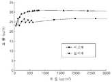
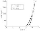
상기 실시예 및 비교예에 대하여 전류-전압 특성 및 휘도-전압을 평가하였다. 도 3 및 4는 각각에 대하여 그래프로 나타낸 것이다. 도 5는 시간에 따른 휘도 특성에 대한 평가 결과이다. 상기 효율 특성 평가에는 PR650 (키앤스社)를 사용하였고, 전류-전압 평가에는 keithly236을 사용하였다.The current-voltage characteristics and the luminance-voltage were evaluated for the above Examples and Comparative Examples. 3 and 4 are graphical representations of each. 5 is an evaluation result of the luminance characteristics over time. PR650 (Keyns, Inc.) was used for the efficiency characteristic evaluation, and keithly236 was used for the current-voltage evaluation.
본 발명에 의한 정공주입층 형성 재료로 사용한 결과, 전하의 주입 능력이 향상됨으로 인해 동일전류치에서 구동전압이 낮아졌으며, 전류효율 (Current Efficiency)값이 향상되었고 이에 따른 휘도값의 증가되었으며, 또한 수명 증가를 확인할 수 있었다.As a result of using the hole injection layer forming material according to the present invention, the driving voltage was lowered at the same current value due to the improved charge injection ability, the current efficiency value was improved and the luminance value was increased accordingly, and the lifetime was also increased. An increase could be confirmed.
도 1a 내지 1c는 본 발명의 구현예들에 따른 유기 발광 소자의 구조를 간략하게 나타낸 단면도이다.1A to 1C are cross-sectional views briefly illustrating a structure of an organic light emitting diode according to embodiments of the present invention.
도 2a는 본 발명의 다른 구현예에 따른 유기 발광 소자의 층들의 HOMO 레벨 및 LUMO 레벨의 차이를 개략적으로 도시한 에너지밴드 다이어그램이다.2A is an energy band diagram schematically illustrating a difference between a HOMO level and a LUMO level of layers of an organic light emitting diode according to another embodiment of the present invention.
도 2b는 본 발명의 또 다른 구현예에 따른 유기 발광 소자의 층들의 HOMO 레벨 및 LUMO 레벨의 차이를 개략적으로 도시한 에너지밴드 다이어그램이다.2B is an energy band diagram schematically illustrating a difference between a HOMO level and a LUMO level of layers of an organic light emitting diode according to another embodiment of the present invention.
도 3은 본 발명의 일 구현예 및 종래 유기 발광 소자의 효율 특성을 측정한 그래프이다.3 is a graph measuring efficiency characteristics of an embodiment of the present invention and a conventional organic light emitting device.
도 4는 본 발명의 일 구현예 및 종래 유기 발광 소자의 전압에 따른 휘도를 측정한 그래프이다.4 is a graph measuring luminance according to voltage of an embodiment of the present invention and a conventional organic light emitting diode.
도 5는 시간에 따른 휘도 특성을 측정하여 나타낸 그래프이다.5 is a graph illustrating measurement of luminance characteristics over time.
Claims (9)
Translated fromKoreanPriority Applications (5)
| Application Number | Priority Date | Filing Date | Title |
|---|---|---|---|
| KR1020070098380AKR100879476B1 (en) | 2007-09-28 | 2007-09-28 | Organic light emitting device |
| US12/133,802US20090085470A1 (en) | 2007-09-28 | 2008-06-05 | Organic light emitting device |
| EP08253107AEP2043174A1 (en) | 2007-09-28 | 2008-09-23 | Organic light emitting device |
| CNA2008101614096ACN101399317A (en) | 2007-09-28 | 2008-09-25 | organic light emitting device |
| JP2008249204AJP2009088525A (en) | 2007-09-28 | 2008-09-26 | Organic light emitting device |
Applications Claiming Priority (1)
| Application Number | Priority Date | Filing Date | Title |
|---|---|---|---|
| KR1020070098380AKR100879476B1 (en) | 2007-09-28 | 2007-09-28 | Organic light emitting device |
Publications (1)
| Publication Number | Publication Date |
|---|---|
| KR100879476B1true KR100879476B1 (en) | 2009-01-20 |
Family
ID=40139135
Family Applications (1)
| Application Number | Title | Priority Date | Filing Date |
|---|---|---|---|
| KR1020070098380AActiveKR100879476B1 (en) | 2007-09-28 | 2007-09-28 | Organic light emitting device |
Country Status (5)
| Country | Link |
|---|---|
| US (1) | US20090085470A1 (en) |
| EP (1) | EP2043174A1 (en) |
| JP (1) | JP2009088525A (en) |
| KR (1) | KR100879476B1 (en) |
| CN (1) | CN101399317A (en) |
Cited By (2)
| Publication number | Priority date | Publication date | Assignee | Title |
|---|---|---|---|---|
| KR20130040709A (en)* | 2011-10-14 | 2013-04-24 | 엘지디스플레이 주식회사 | Organic light emitting device and display panel using the same |
| US9165980B2 (en) | 2013-01-04 | 2015-10-20 | Samsung Display Co., Ltd. | Organic light-emitting device and of preparing the same |
Families Citing this family (8)
| Publication number | Priority date | Publication date | Assignee | Title |
|---|---|---|---|---|
| KR101135541B1 (en) | 2010-04-01 | 2012-04-13 | 삼성모바일디스플레이주식회사 | Organic light emitting diode device |
| JP5867681B2 (en)* | 2011-09-02 | 2016-02-24 | 国立大学法人群馬大学 | Oxygen sensor based on the ratio method |
| CN103050641B (en)* | 2011-10-14 | 2016-03-02 | 乐金显示有限公司 | The display panel of organic luminescent device and this device of use |
| CN103367644A (en)* | 2012-04-11 | 2013-10-23 | 海洋王照明科技股份有限公司 | Organic electroluminescent device and preparation method thereof |
| KR102083982B1 (en)* | 2013-10-29 | 2020-04-16 | 삼성디스플레이 주식회사 | Organic light emitting device and manufacturing method thereof |
| JP7421284B2 (en)* | 2019-08-09 | 2024-01-24 | JDI Design and Development 合同会社 | Display panel and display panel manufacturing method |
| KR102719790B1 (en)* | 2019-11-11 | 2024-10-22 | 삼성디스플레이 주식회사 | Display device |
| CN114586187A (en)* | 2020-09-28 | 2022-06-03 | 京东方科技集团股份有限公司 | Organic electroluminescent device and display device |
Citations (4)
| Publication number | Priority date | Publication date | Assignee | Title |
|---|---|---|---|---|
| JP2004355975A (en) | 2003-05-29 | 2004-12-16 | Sony Corp | Manufacturing method of display device |
| KR20060007899A (en)* | 2004-07-22 | 2006-01-26 | 삼성에스디아이 주식회사 | Organic electroluminescent device and manufacturing method thereof |
| KR20060042177A (en)* | 2004-03-01 | 2006-05-12 | 가부시끼가이샤 아이메스 | Organic light emitting diode |
| JP2006156344A (en) | 2004-09-24 | 2006-06-15 | Semiconductor Energy Lab Co Ltd | Light emitting device |
Family Cites Families (28)
| Publication number | Priority date | Publication date | Assignee | Title |
|---|---|---|---|---|
| JP4505067B2 (en)* | 1998-12-16 | 2010-07-14 | 淳二 城戸 | Organic electroluminescent device |
| US7306856B2 (en)* | 2000-07-17 | 2007-12-11 | Fujifilm Corporation | Light-emitting element and iridium complex |
| US7033680B2 (en)* | 2001-11-30 | 2006-04-25 | Sumitomo Chemical Company, Limited | Electroluminescent element |
| KR100501702B1 (en)* | 2003-03-13 | 2005-07-18 | 삼성에스디아이 주식회사 | Organic electroluminescent display device |
| JP3877692B2 (en)* | 2003-03-28 | 2007-02-07 | 三洋電機株式会社 | Organic electroluminescence device and method for manufacturing the same |
| KR100560778B1 (en)* | 2003-04-17 | 2006-03-13 | 삼성에스디아이 주식회사 | Organic electroluminescent display device |
| KR20050015902A (en)* | 2003-08-14 | 2005-02-21 | 엘지전자 주식회사 | Organic electroluminescence device and fabrication method of the same |
| JP3748110B1 (en)* | 2003-09-26 | 2006-02-22 | 株式会社半導体エネルギー研究所 | LIGHT EMITTING DEVICE AND ELECTRONIC DEVICE USING THE SAME |
| EP1722602A1 (en)* | 2004-03-05 | 2006-11-15 | Idemitsu Kosan Co., Ltd. | Organic electroluminescent device and organic electroluminescent display |
| US7195829B2 (en)* | 2004-03-30 | 2007-03-27 | Eastman Kodak Company | Organic element for electroluminescent devices |
| US20060008670A1 (en)* | 2004-07-06 | 2006-01-12 | Chun Lin | Organic light emitting materials and devices |
| JP4925569B2 (en)* | 2004-07-08 | 2012-04-25 | ローム株式会社 | Organic electroluminescent device |
| US7750560B2 (en)* | 2004-10-01 | 2010-07-06 | Semiconductor Energy Laboratory Co., Ltd. | Light-emitting-element |
| US7687986B2 (en)* | 2005-05-27 | 2010-03-30 | Fujifilm Corporation | Organic EL device having hole-injection layer doped with metallic oxide |
| US20060286405A1 (en)* | 2005-06-17 | 2006-12-21 | Eastman Kodak Company | Organic element for low voltage electroluminescent devices |
| US8017252B2 (en)* | 2005-06-22 | 2011-09-13 | Semiconductor Energy Laboratory Co., Ltd. | Light emitting device and electronic appliance using the same |
| KR100806812B1 (en)* | 2005-07-25 | 2008-02-25 | 엘지.필립스 엘시디 주식회사 | Organic EL element and its manufacturing method |
| KR20070036835A (en)* | 2005-09-30 | 2007-04-04 | 삼성전자주식회사 | Method for manufacturing an organic light emitting device comprising an inorganic buffer layer |
| US20070090756A1 (en)* | 2005-10-11 | 2007-04-26 | Fujifilm Corporation | Organic electroluminescent element |
| JP2007109868A (en)* | 2005-10-13 | 2007-04-26 | Sanyo Electric Co Ltd | Thin film transistor and organic electroluminescence display device |
| TWI299636B (en)* | 2005-12-01 | 2008-08-01 | Au Optronics Corp | Organic light emitting diode |
| US8454748B2 (en)* | 2005-12-27 | 2013-06-04 | Semiconductor Energy Laboratory Co., Ltd. | Method of calculating carrier mobility |
| US7968904B2 (en)* | 2006-02-06 | 2011-06-28 | Fujifilm Corporation | Organic electroluminescence device |
| US9112170B2 (en)* | 2006-03-21 | 2015-08-18 | Semiconductor Energy Laboratory Co., Ltd. | Light-emitting element, light-emitting device, and electronic device |
| US20090128024A1 (en)* | 2006-04-20 | 2009-05-21 | Kenichi Fukuoka | Organic light-emitting device |
| KR100922755B1 (en)* | 2007-12-28 | 2009-10-21 | 삼성모바일디스플레이주식회사 | Organic light emitting device |
| KR100894066B1 (en)* | 2007-12-28 | 2009-04-24 | 삼성모바일디스플레이 주식회사 | Organic light emitting device |
| KR100922760B1 (en)* | 2008-03-03 | 2009-10-21 | 삼성모바일디스플레이주식회사 | Organic light emitting device |
- 2007
- 2007-09-28KRKR1020070098380Apatent/KR100879476B1/enactiveActive
- 2008
- 2008-06-05USUS12/133,802patent/US20090085470A1/ennot_activeAbandoned
- 2008-09-23EPEP08253107Apatent/EP2043174A1/ennot_activeWithdrawn
- 2008-09-25CNCNA2008101614096Apatent/CN101399317A/enactivePending
- 2008-09-26JPJP2008249204Apatent/JP2009088525A/enactivePending
Patent Citations (4)
| Publication number | Priority date | Publication date | Assignee | Title |
|---|---|---|---|---|
| JP2004355975A (en) | 2003-05-29 | 2004-12-16 | Sony Corp | Manufacturing method of display device |
| KR20060042177A (en)* | 2004-03-01 | 2006-05-12 | 가부시끼가이샤 아이메스 | Organic light emitting diode |
| KR20060007899A (en)* | 2004-07-22 | 2006-01-26 | 삼성에스디아이 주식회사 | Organic electroluminescent device and manufacturing method thereof |
| JP2006156344A (en) | 2004-09-24 | 2006-06-15 | Semiconductor Energy Lab Co Ltd | Light emitting device |
Cited By (4)
| Publication number | Priority date | Publication date | Assignee | Title |
|---|---|---|---|---|
| KR20130040709A (en)* | 2011-10-14 | 2013-04-24 | 엘지디스플레이 주식회사 | Organic light emitting device and display panel using the same |
| KR102066074B1 (en)* | 2011-10-14 | 2020-01-14 | 엘지디스플레이 주식회사 | Organic light emitting device and display panel using the same |
| US9165980B2 (en) | 2013-01-04 | 2015-10-20 | Samsung Display Co., Ltd. | Organic light-emitting device and of preparing the same |
| USRE47578E1 (en) | 2013-01-04 | 2019-08-20 | Samsung Display Co., Ltd. | Organic light-emitting device and of preparing the same |
Also Published As
| Publication number | Publication date |
|---|---|
| EP2043174A1 (en) | 2009-04-01 |
| JP2009088525A (en) | 2009-04-23 |
| US20090085470A1 (en) | 2009-04-02 |
| CN101399317A (en) | 2009-04-01 |
Similar Documents
| Publication | Publication Date | Title |
|---|---|---|
| KR100918401B1 (en) | Organic light emitting device | |
| KR100922760B1 (en) | Organic light emitting device | |
| KR100922759B1 (en) | Organic light emitting device | |
| KR100879476B1 (en) | Organic light emitting device | |
| KR100922755B1 (en) | Organic light emitting device | |
| KR100670383B1 (en) | Organic light emitting device and flat panel display device having the same | |
| KR100894066B1 (en) | Organic light emitting device | |
| JP4722695B2 (en) | Organic light emitting device | |
| KR20090050369A (en) | Organic light emitting device | |
| KR100898075B1 (en) | Organic light emitting device | |
| KR20070087773A (en) | Organic light emitting device and flat panel display device having the same | |
| KR20090131550A (en) | Organic light emitting device | |
| KR100730221B1 (en) | Organic light emitting device and flat panel display device having the same | |
| KR100751366B1 (en) | White light-emitting organic light emitting diode and flat panel display device having the same | |
| KR100751357B1 (en) | Organic light emitting device and flat panel display device having the same | |
| KR100670369B1 (en) | Organic EL device and flat panel display device having the same | |
| KR101202344B1 (en) | An organic light emitting device and a flat display device comprising the same | |
| KR100741075B1 (en) | Flat panel display and manufacturing method thereof |
Legal Events
| Date | Code | Title | Description |
|---|---|---|---|
| A201 | Request for examination | ||
| PA0109 | Patent application | Patent event code:PA01091R01D Comment text:Patent Application Patent event date:20070928 | |
| PA0201 | Request for examination | ||
| E902 | Notification of reason for refusal | ||
| PE0902 | Notice of grounds for rejection | Comment text:Notification of reason for refusal Patent event date:20080627 Patent event code:PE09021S01D | |
| N231 | Notification of change of applicant | ||
| PN2301 | Change of applicant | Patent event date:20081120 Comment text:Notification of Change of Applicant Patent event code:PN23011R01D | |
| E701 | Decision to grant or registration of patent right | ||
| PE0701 | Decision of registration | Patent event code:PE07011S01D Comment text:Decision to Grant Registration Patent event date:20081229 | |
| GRNT | Written decision to grant | ||
| PR0701 | Registration of establishment | Comment text:Registration of Establishment Patent event date:20090113 Patent event code:PR07011E01D | |
| PR1002 | Payment of registration fee | Payment date:20090114 End annual number:3 Start annual number:1 | |
| PG1601 | Publication of registration | ||
| PR1001 | Payment of annual fee | Payment date:20111216 Start annual number:4 End annual number:4 | |
| FPAY | Annual fee payment | Payment date:20130102 Year of fee payment:5 | |
| PR1001 | Payment of annual fee | Payment date:20130102 Start annual number:5 End annual number:5 | |
| FPAY | Annual fee payment | Payment date:20140102 Year of fee payment:6 | |
| PR1001 | Payment of annual fee | Payment date:20140102 Start annual number:6 End annual number:6 | |
| FPAY | Annual fee payment | Payment date:20141231 Year of fee payment:7 | |
| PR1001 | Payment of annual fee | Payment date:20141231 Start annual number:7 End annual number:7 | |
| FPAY | Annual fee payment | Payment date:20151230 Year of fee payment:8 | |
| PR1001 | Payment of annual fee | Payment date:20151230 Start annual number:8 End annual number:8 | |
| FPAY | Annual fee payment | Payment date:20170102 Year of fee payment:9 | |
| PR1001 | Payment of annual fee | Payment date:20170102 Start annual number:9 End annual number:9 | |
| FPAY | Annual fee payment | Payment date:20180102 Year of fee payment:10 | |
| PR1001 | Payment of annual fee | Payment date:20180102 Start annual number:10 End annual number:10 | |
| FPAY | Annual fee payment | Payment date:20190102 Year of fee payment:11 | |
| PR1001 | Payment of annual fee | Payment date:20190102 Start annual number:11 End annual number:11 | |
| PR1001 | Payment of annual fee | Payment date:20210104 Start annual number:13 End annual number:13 | |
| PR1001 | Payment of annual fee | Payment date:20211228 Start annual number:14 End annual number:14 | |
| PR1001 | Payment of annual fee | Payment date:20221226 Start annual number:15 End annual number:15 |