KR100878790B1 - Active matrix image display device and image display method using same - Google Patents
Active matrix image display device and image display method using sameDownload PDFInfo
- Publication number
- KR100878790B1 KR100878790B1KR1020020053635AKR20020053635AKR100878790B1KR 100878790 B1KR100878790 B1KR 100878790B1KR 1020020053635 AKR1020020053635 AKR 1020020053635AKR 20020053635 AKR20020053635 AKR 20020053635AKR 100878790 B1KR100878790 B1KR 100878790B1
- Authority
- KR
- South Korea
- Prior art keywords
- pixel
- liquid crystal
- area
- substrate
- data
- Prior art date
- Legal status (The legal status is an assumption and is not a legal conclusion. Google has not performed a legal analysis and makes no representation as to the accuracy of the status listed.)
- Expired - Lifetime
Links
Images


Classifications
- G—PHYSICS
- G02—OPTICS
- G02F—OPTICAL DEVICES OR ARRANGEMENTS FOR THE CONTROL OF LIGHT BY MODIFICATION OF THE OPTICAL PROPERTIES OF THE MEDIA OF THE ELEMENTS INVOLVED THEREIN; NON-LINEAR OPTICS; FREQUENCY-CHANGING OF LIGHT; OPTICAL LOGIC ELEMENTS; OPTICAL ANALOGUE/DIGITAL CONVERTERS
- G02F1/00—Devices or arrangements for the control of the intensity, colour, phase, polarisation or direction of light arriving from an independent light source, e.g. switching, gating or modulating; Non-linear optics
- G02F1/01—Devices or arrangements for the control of the intensity, colour, phase, polarisation or direction of light arriving from an independent light source, e.g. switching, gating or modulating; Non-linear optics for the control of the intensity, phase, polarisation or colour
- G02F1/13—Devices or arrangements for the control of the intensity, colour, phase, polarisation or direction of light arriving from an independent light source, e.g. switching, gating or modulating; Non-linear optics for the control of the intensity, phase, polarisation or colour based on liquid crystals, e.g. single liquid crystal display cells
- G02F1/133—Constructional arrangements; Operation of liquid crystal cells; Circuit arrangements
- G02F1/136—Liquid crystal cells structurally associated with a semi-conducting layer or substrate, e.g. cells forming part of an integrated circuit
- G02F1/1362—Active matrix addressed cells
- G—PHYSICS
- G02—OPTICS
- G02F—OPTICAL DEVICES OR ARRANGEMENTS FOR THE CONTROL OF LIGHT BY MODIFICATION OF THE OPTICAL PROPERTIES OF THE MEDIA OF THE ELEMENTS INVOLVED THEREIN; NON-LINEAR OPTICS; FREQUENCY-CHANGING OF LIGHT; OPTICAL LOGIC ELEMENTS; OPTICAL ANALOGUE/DIGITAL CONVERTERS
- G02F1/00—Devices or arrangements for the control of the intensity, colour, phase, polarisation or direction of light arriving from an independent light source, e.g. switching, gating or modulating; Non-linear optics
- G02F1/01—Devices or arrangements for the control of the intensity, colour, phase, polarisation or direction of light arriving from an independent light source, e.g. switching, gating or modulating; Non-linear optics for the control of the intensity, phase, polarisation or colour
- G02F1/13—Devices or arrangements for the control of the intensity, colour, phase, polarisation or direction of light arriving from an independent light source, e.g. switching, gating or modulating; Non-linear optics for the control of the intensity, phase, polarisation or colour based on liquid crystals, e.g. single liquid crystal display cells
- G02F1/133—Constructional arrangements; Operation of liquid crystal cells; Circuit arrangements
- G02F1/1333—Constructional arrangements; Manufacturing methods
- G02F1/1335—Structural association of cells with optical devices, e.g. polarisers or reflectors
- G02F1/133509—Filters, e.g. light shielding masks
- G02F1/133514—Colour filters
- G—PHYSICS
- G02—OPTICS
- G02F—OPTICAL DEVICES OR ARRANGEMENTS FOR THE CONTROL OF LIGHT BY MODIFICATION OF THE OPTICAL PROPERTIES OF THE MEDIA OF THE ELEMENTS INVOLVED THEREIN; NON-LINEAR OPTICS; FREQUENCY-CHANGING OF LIGHT; OPTICAL LOGIC ELEMENTS; OPTICAL ANALOGUE/DIGITAL CONVERTERS
- G02F1/00—Devices or arrangements for the control of the intensity, colour, phase, polarisation or direction of light arriving from an independent light source, e.g. switching, gating or modulating; Non-linear optics
- G02F1/01—Devices or arrangements for the control of the intensity, colour, phase, polarisation or direction of light arriving from an independent light source, e.g. switching, gating or modulating; Non-linear optics for the control of the intensity, phase, polarisation or colour
- G02F1/13—Devices or arrangements for the control of the intensity, colour, phase, polarisation or direction of light arriving from an independent light source, e.g. switching, gating or modulating; Non-linear optics for the control of the intensity, phase, polarisation or colour based on liquid crystals, e.g. single liquid crystal display cells
- G02F1/133—Constructional arrangements; Operation of liquid crystal cells; Circuit arrangements
- G—PHYSICS
- G09—EDUCATION; CRYPTOGRAPHY; DISPLAY; ADVERTISING; SEALS
- G09G—ARRANGEMENTS OR CIRCUITS FOR CONTROL OF INDICATING DEVICES USING STATIC MEANS TO PRESENT VARIABLE INFORMATION
- G09G3/00—Control arrangements or circuits, of interest only in connection with visual indicators other than cathode-ray tubes
- G09G3/20—Control arrangements or circuits, of interest only in connection with visual indicators other than cathode-ray tubes for presentation of an assembly of a number of characters, e.g. a page, by composing the assembly by combination of individual elements arranged in a matrix no fixed position being assigned to or needed to be assigned to the individual characters or partial characters
- G09G3/34—Control arrangements or circuits, of interest only in connection with visual indicators other than cathode-ray tubes for presentation of an assembly of a number of characters, e.g. a page, by composing the assembly by combination of individual elements arranged in a matrix no fixed position being assigned to or needed to be assigned to the individual characters or partial characters by control of light from an independent source
- G09G3/36—Control arrangements or circuits, of interest only in connection with visual indicators other than cathode-ray tubes for presentation of an assembly of a number of characters, e.g. a page, by composing the assembly by combination of individual elements arranged in a matrix no fixed position being assigned to or needed to be assigned to the individual characters or partial characters by control of light from an independent source using liquid crystals
- G09G3/3611—Control of matrices with row and column drivers
- G09G3/3648—Control of matrices with row and column drivers using an active matrix
- G—PHYSICS
- G02—OPTICS
- G02F—OPTICAL DEVICES OR ARRANGEMENTS FOR THE CONTROL OF LIGHT BY MODIFICATION OF THE OPTICAL PROPERTIES OF THE MEDIA OF THE ELEMENTS INVOLVED THEREIN; NON-LINEAR OPTICS; FREQUENCY-CHANGING OF LIGHT; OPTICAL LOGIC ELEMENTS; OPTICAL ANALOGUE/DIGITAL CONVERTERS
- G02F1/00—Devices or arrangements for the control of the intensity, colour, phase, polarisation or direction of light arriving from an independent light source, e.g. switching, gating or modulating; Non-linear optics
- G02F1/01—Devices or arrangements for the control of the intensity, colour, phase, polarisation or direction of light arriving from an independent light source, e.g. switching, gating or modulating; Non-linear optics for the control of the intensity, phase, polarisation or colour
- G02F1/13—Devices or arrangements for the control of the intensity, colour, phase, polarisation or direction of light arriving from an independent light source, e.g. switching, gating or modulating; Non-linear optics for the control of the intensity, phase, polarisation or colour based on liquid crystals, e.g. single liquid crystal display cells
- G02F1/133—Constructional arrangements; Operation of liquid crystal cells; Circuit arrangements
- G02F1/1333—Constructional arrangements; Manufacturing methods
- G02F1/133388—Constructional arrangements; Manufacturing methods with constructional differences between the display region and the peripheral region
- G—PHYSICS
- G02—OPTICS
- G02F—OPTICAL DEVICES OR ARRANGEMENTS FOR THE CONTROL OF LIGHT BY MODIFICATION OF THE OPTICAL PROPERTIES OF THE MEDIA OF THE ELEMENTS INVOLVED THEREIN; NON-LINEAR OPTICS; FREQUENCY-CHANGING OF LIGHT; OPTICAL LOGIC ELEMENTS; OPTICAL ANALOGUE/DIGITAL CONVERTERS
- G02F1/00—Devices or arrangements for the control of the intensity, colour, phase, polarisation or direction of light arriving from an independent light source, e.g. switching, gating or modulating; Non-linear optics
- G02F1/01—Devices or arrangements for the control of the intensity, colour, phase, polarisation or direction of light arriving from an independent light source, e.g. switching, gating or modulating; Non-linear optics for the control of the intensity, phase, polarisation or colour
- G02F1/13—Devices or arrangements for the control of the intensity, colour, phase, polarisation or direction of light arriving from an independent light source, e.g. switching, gating or modulating; Non-linear optics for the control of the intensity, phase, polarisation or colour based on liquid crystals, e.g. single liquid crystal display cells
- G02F1/133—Constructional arrangements; Operation of liquid crystal cells; Circuit arrangements
- G02F1/136—Liquid crystal cells structurally associated with a semi-conducting layer or substrate, e.g. cells forming part of an integrated circuit
- G02F1/1362—Active matrix addressed cells
- G02F1/136286—Wiring, e.g. gate line, drain line
- G—PHYSICS
- G09—EDUCATION; CRYPTOGRAPHY; DISPLAY; ADVERTISING; SEALS
- G09G—ARRANGEMENTS OR CIRCUITS FOR CONTROL OF INDICATING DEVICES USING STATIC MEANS TO PRESENT VARIABLE INFORMATION
- G09G2310/00—Command of the display device
- G09G2310/02—Addressing, scanning or driving the display screen or processing steps related thereto
- G09G2310/0232—Special driving of display border areas
Landscapes
- Physics & Mathematics (AREA)
- Nonlinear Science (AREA)
- Chemical & Material Sciences (AREA)
- Crystallography & Structural Chemistry (AREA)
- General Physics & Mathematics (AREA)
- Engineering & Computer Science (AREA)
- Optics & Photonics (AREA)
- Mathematical Physics (AREA)
- Computer Hardware Design (AREA)
- Theoretical Computer Science (AREA)
- Microelectronics & Electronic Packaging (AREA)
- Control Of Indicators Other Than Cathode Ray Tubes (AREA)
- Liquid Crystal Display Device Control (AREA)
- Devices For Indicating Variable Information By Combining Individual Elements (AREA)
- Liquid Crystal (AREA)
Abstract
Translated fromKorean
Description
Translated fromKorean도 1은 본 발명의 바람직한 일실시예에 따른 테두리 라인을 표시하기 위한 액정 표시 장치의 개략도이다.1 is a schematic diagram of a liquid crystal display for displaying an edge line according to an exemplary embodiment of the present invention.
도 2는 도 1에 도시한 액정 표시 장치를 사용하여 액정 표시 패널에 테두리 라인이 디스플레이 되는 상태를 도면이다.FIG. 2 is a diagram illustrating a state in which an edge line is displayed on the liquid crystal display panel using the liquid crystal display shown in FIG. 1.
도 3은 도 1에 도시한 액정 표시 장치를 이용하여 테두리 라인을 표시하기 위하여 액정 표시 패널에 인가되는 R.G.B. 신호를 나타낸 도면이다.FIG. 3 is an R.G.B. applied to a liquid crystal display panel to display an edge line using the liquid crystal display shown in FIG. A diagram showing a signal.
도 4는 도 1에 도시한 액정 표시 장치를 이용하여 테두리 라인을 표시하기 위하여 소스 구동부를 통하여 액정 표시 패널에 인가되는 R.G.B. 신호를 나타낸 도면이다.FIG. 4 is an R.G.B. applied to a liquid crystal display panel through a source driver to display an edge line using the liquid crystal display shown in FIG. A diagram showing a signal.
도 5a 내지 도 5c는 본 발명에 따른 테두리 라인을 표시하기 위하여 액정 표시 패널의 테두리 라인에 상응하는 박막 트랜지스터의 등가 회로도이다.5A to 5C are equivalent circuit diagrams of a thin film transistor corresponding to a border line of a liquid crystal display panel in order to display a border line according to the present invention.
도 6a 내지 도 6c는 도 5a 내지 도 5c의 박막 트랜지스터를 구현한 액정 표시 패널의 단면도이다.6A through 6C are cross-sectional views of a liquid crystal display panel implementing the thin film transistors of FIGS. 5A through 5C.
도 7은 테두리 라인을 표시하기 위하여 액정 표시 패널에 색화소를 형성할 경우 본 발명의 바람직한 제1 실시예에 따른 색화소가 형성된 액정 표시 패널의 개략도이다.7 is a schematic diagram of a liquid crystal display panel in which a color pixel according to the first exemplary embodiment of the present invention is formed when color pixels are formed in the liquid crystal display panel to display edge lines.
도 8은 테두리 라인을 표시하기 위하여 액정 표시 패널에 색화소를 형성할 경우 본 발명의 바람직한 제2 실시예에 따른 색화소가 형성된 액정 표시 패널의 개략도이다.8 is a schematic diagram of a liquid crystal display panel in which a color pixel according to a second exemplary embodiment of the present invention is formed when color pixels are formed in the liquid crystal display panel to display edge lines.
도 9는 테두리 라인을 표시하기 위하여 액정 표시 패널에 색화소를 형성할 경우 본 발명의 바람직한 제3 실시예에 따른 색화소가 형성된 액정 표시 패널의 개략도이다.9 is a schematic diagram of a liquid crystal display panel in which a color pixel according to a third exemplary embodiment of the present invention is formed when color pixels are formed in the liquid crystal display panel to display an edge line.
도 10은 테두리 라인을 표시하기 위하여 액정 표시 패널에 색화소를 형성할 경우 본 발명의 바람직한 제4 실시예에 따른 색화소가 형성된 액정 표시 패널의 개략도이다.10 is a schematic view of a liquid crystal display panel in which a color pixel according to a fourth exemplary embodiment of the present invention is formed when color pixels are formed in the liquid crystal display panel to display edge lines.
도 11은 테두리 라인을 표시하기 위하여 액정 표시 패널에 색화소를 형성할 경우 본 발명의 바람직한 제5 실시예에 따른 색화소가 형성된 액정 표시 패널의 개략도이다.FIG. 11 is a schematic diagram of a liquid crystal display panel in which a color pixel according to a fifth exemplary embodiment of the present invention is formed when color pixels are formed in a liquid crystal display panel to display an edge line.
<도면의 주요부분에 대한 부호의 설명><Description of the symbols for the main parts of the drawings>
30 : 타이밍 제어부40 : 소스 구동부30: timing controller 40: source driver
50 : 게이트 구동부60 : 액정 표시 패널50: gate driver 60: liquid crystal display panel
102 : 소스 전극106: 게이트 전극102: source electrode 106: gate electrode
108 : 드레인 전극110 : 박막 트랜지스터 기판108: drain electrode 110: thin film transistor substrate
112 : 화소 전극114 : 박막 트랜지스터112
120 : 액정 층170 : 칼라 필터 기판120: liquid crystal layer 170: color filter substrate
174 : 색화소176 : 공통 전극
174: color pixel 176: common electrode
본 발명은 액티브 매트릭스 방식의 화상 표시 장치 및 이를 이용한 화상 표시 방법에 관한 것으로, 특히 테두리 라인 디스플레이 기능을 가지는 액티브 매트릭스 방식의 화상 표시 장치 및 이를 이용한 화상 표시 방법에 관한 것이다.The present invention relates to an active matrix image display device and an image display method using the same, and more particularly, to an active matrix image display device having an edge line display function and an image display method using the same.
종래의 대표적인 CRT방식의 디스플레이 장치에 비하여, 최근에는 얇고, 가벼우면서도 저소비전력의 특징을 가지는 액정 표시 장치, 유기 EL(Organic Electroluminescent) 디스플레이 장치, 플라즈마 디스플레이 패널(Plasma Display Panel) 등의 평판 패널형 전자 디스플레이 장치(FPD; Flat Panel Display) 대한 수요가 급격히 증가하고 있다. 이와 같은 수요에 적합한 평판 패널형 전자 디스플레이 장치에 대한 연구 개발이 진행되어 실용화되고 있다. 특히, 액정 표시 장치는 전 세계적으로 수요가 급증하고 있는 대표적인 디스플레이 장치이다.Compared to conventional CRT display devices, flat panel electronics such as liquid crystal displays, organic EL (Organic Electroluminescent) displays, and plasma display panels, which are thin, light, and low in power consumption, have recently been characterized. The demand for flat panel displays (FPDs) is rapidly increasing. Research and development on a flat panel type electronic display device suitable for such a demand has been progressed and put into practical use. In particular, the liquid crystal display is a representative display device that demand is increasing worldwide.
액정 표시 장치는 구동방식의 차이에 따라 스위칭 소자 및 TN액정을 이용한 액티브 매트릭스(Active matrix)표시방식과 STN 액정을 이용한 패시브 매트릭스(passive matrix)표시 방식으로 구분할 수 있다.The liquid crystal display may be classified into an active matrix display method using a switching element and a TN liquid crystal and a passive matrix display method using an STN liquid crystal according to a difference in driving method.
액티브 매트릭스 표시 방식은 스위칭 소자인 트랜지스터를 이용하여 구동하 는 방식으로서, 상기와 같은 스위칭 소자를 구동하기 위하여 별도의 구동 회로가 필요하다. 액티브 매트릭스 표시 방식은 액정 표시 장치 및 유기 EL 등에 적용될 수 있다. 반면에 패시브 매트릭스 표시방식에서는 스위칭 소자인 트랜지스터를 사용하지 않기 때문에 이와 관련한 복잡한 회로를 필요로 하지 않는다.The active matrix display method is a method of driving using a transistor which is a switching element, and a separate driving circuit is required to drive the switching element as described above. The active matrix display method can be applied to a liquid crystal display device and an organic EL. On the other hand, the passive matrix display method does not use a transistor, which is a switching element, and thus does not require a complicated circuit.
이와 같은 액티브 매트릭스 표시 방법을 사용하는 디스플레이 장치에 있어서, 표시 영역(display area)에는 문자, 숫자 외에 정지 화상, 동영상 등의 화상 데이터가 디스플레이 된다. 최근에는 표시 영역에 화상 데이터 등을 디스플레이 할 경우 깔끔한 화면 처리 효과와 액자와 같은 분위기를 연출할 수 있는 테두리 라인을 함께 디스플레이 하고자 하는 요구가 있다.In a display device using such an active matrix display method, image data such as still images, moving images, and the like, in addition to letters and numbers are displayed in a display area. Recently, when displaying image data and the like on the display area, there is a demand for displaying a neat screen processing effect and a border line that can create a frame-like atmosphere.
액티브 매트릭스 방식을 이용하여 소정의 색깔을 가지는 테두리 라인을 디스플레이 하기 위해서는 별도의 테두리 라인 신호를 발생하기 위한 구동 회로가 부가되거나 기존의 액티브 매트릭스 구동 회로를 변경해야만 하는 문제점이 있었다.In order to display a border line having a predetermined color by using an active matrix method, there is a problem in that a driving circuit for generating a separate border line signal is added or an existing active matrix driving circuit must be changed.
본 발명의 제1 목적은 이와 같은 종래 기술의 문제점을 해결하기 위하여 액티브 매트릭스 구동 방식의 화면 표시 장치에 있어서, 별도의 부가회로나 기존의 액티브 매트릭스 구동 회로를 변경하지 않고도 사용자가 직접 원하는 색깔을 설정하여 소정 색깔의 테두리 라인을 디스플레이 할 수 있는 액티브 매트릭스 방식의 화면 표시 장치를 제공함에 있다.In order to solve the problems of the related art, the first object of the present invention is to set a color directly desired by a user without changing an additional circuit or an existing active matrix driving circuit in an active matrix driving screen display device. The present invention provides an active matrix screen display device capable of displaying a border line of a predetermined color.
또한, 본 발명의 제2 목적은 사용자가 직접 원하는 색깔을 설정하여 소정 색깔의 테두리 라인을 디스플레이 할 수 있는 화면 표시 장치의 화상 디스플레이 방 법을 제공함에 있다.
In addition, a second object of the present invention is to provide an image display method of a screen display device that can display a border line of a predetermined color by setting a desired color directly.
상기한 본 발명의 제1 목적을 달성하기 위하여 본 발명은 제1 기판과, 상기 제1 기판과 대향하도록 배치되는 제2 기판과, 화상이 디스플레이 되는 표시 영역 중 테두리를 나타내는 제1 영역에 상응하는 상기 제2 기판의 상면에 형성된 제1 색화소와, 상기 표시 영역 중 상기 제1 영역을 제외한 제2 영역에 상응하는 상기 제2 기판의 상면에 형성된 제2 색화소와, 상기 1 영역 내에 포함되고, 상기 제1 기판과 상기 제2 기판 사이에 개재되며 화상을 디스플레이 할 경우 무전계가 형성되어 광이 전부 투과되도록 하는 제1 액정과, 상기 2 영역 내에 포함되고, 상기 제1 기판과 상기 제2 기판 사이에 개재되는 제2 액정을 포함하는 액정 표시 장치를 제공한다.In order to achieve the first object of the present invention, the present invention corresponds to a first substrate, a second substrate disposed to face the first substrate, and a first region representing an edge of a display region in which an image is displayed. A first color pixel formed on an upper surface of the second substrate, a second color pixel formed on an upper surface of the second substrate corresponding to a second area except the first area of the display area, and included in the first area A first liquid crystal interposed between the first substrate and the second substrate and configured to form an electromagnetic field so that all of the light passes through the first substrate and the second substrate, and included in the two regions; Provided is a liquid crystal display device including a second liquid crystal interposed therebetween.
또한, 상기 제1 목적을 달성하기 위하여 본 발명은 복수의 행과 열로 이루어진 표시 영역 중 상측 테두리 라인을 나타내는 제1 테두리 영역의 각 화소에 대한 색 정보를 포함하는 제1 더미 라인 데이터, 상기 제1 테두리 영역에 대향하는 하측 테두리 라인을 나타내는 제2 테두리 영역의 각 화소에 대한 색 정보를 포함하는 제2 더미 라인 데이터, 좌측 테두리 라인을 나타내는 제3 테두리 영역의 각 화소에 대한 색 정보를 포함하는 제1 더미 픽셀 데이터 및 우측 테두리 라인을 나타내는 제4 테두리 영역의 각 화소에 대한 색 정보를 포함하는 제2 더미 픽셀 데이터를 발생시키고, 상기 표시 영역 중 상기 상하좌우 테두리 라인을 제외한 영역의 각 화소 에 대한 색 정보를 포함하는 제1 표시 영역 데이터를 입력받아 상기 제1 표시 영역 데이터에 상기 제1 및 제2 더미 픽셀 데이터를 부가한 제2 표시 영역 데이터를 발생시키고, 상기 제1 더미 데이터, 제2 표시 영역 데이터 및 제2 더미 라인 데이터가 상기 표시 영역의 각각의 행에 순차적으로 디스플레이 되도록 하는 제1 제어 신호를 발생시키는 타이밍 제어부와, 상기 타이밍 제어부로부터 제공되는 상기 제1 제어 신호를 근거로 상기 제1 및 제2 테두리 영역으로 각각 상기 제1 더미 라인 데이터 및 제2 더미 라인 데이터를 디스플레이 하도록 제어하는 제1 더미 라인 구동 신호 및 제2 더미 라인 구동 신호를 발생시키고, 상기 제1 제어 신호를 근거로 상기 표시 영역 중 상기 제1 및 제2 테두리 영역을 제외한 나머지 영역에 상기 제2 표시 영역 데이터를 행단위로 디스플레이 하도록 제어하는 복수의 제2 제어 신호를 발생시키는 제1 구동부와, 상기 타이밍 제어부로부터 상기 제1 더미 라인 데이터, 상기 제2 표시 영역 데이터 및 제2 더미 라인 데이터를 입력받고, 상기 제1 더미 라인 구동 신호, 복수의 제2 제어 신호 및 제2 더미 라인 구동 신호에 상응하여 상기 제1 더미 라인 데이터, 제2 표시 영역 데이터 및 제2 더미 라인 데이터를 상기 표시 영역에 디스플레이 되도록 하는 제2 구동부를 포함하는 능동 매트릭스 구동 방식 화면 표시 장치를 제공한다.In addition, in order to achieve the first object, the present invention provides first dummy line data including color information for each pixel of a first edge region representing an upper edge line among a display region including a plurality of rows and columns, and the first dummy line data. Second dummy line data including color information of each pixel of the second border area representing the lower border line opposite to the border area, and second color line data including color information of each pixel of the third border area representing the left border line. Generating second dummy pixel data including first dummy pixel data and color information of each pixel of the fourth border region representing the right edge line, and generating the second dummy pixel data including the first dummy pixel data and the The first and second display area data including color information is input to the first display area data. A first control signal for generating second display area data to which dummy pixel data is added and for causing the first dummy data, the second display area data, and the second dummy line data to be sequentially displayed in each row of the display area; And a first control unit configured to display the first dummy line data and the second dummy line data in the first and second edge regions, respectively, based on the timing control unit generating the first control signal and the first control signal provided from the timing control unit. A dummy line driving signal and a second dummy line driving signal are generated, and the second display area data is displayed in units of rows on the remaining areas of the display area except the first and second edge areas based on the first control signal. A first driver for generating a plurality of second control signals that are controlled to The first dummy line data, the second display area data, and the second dummy line data may be input and correspond to the first dummy line driving signal, a plurality of second control signals, and a second dummy line driving signal. Provided is an active matrix driving screen display device including a second driver configured to display dummy line data, second display area data, and second dummy line data on the display area.
상기 제2 목적을 달성하기 위하여 본 발명은 화상이 디스플레이 되는 표시 영역 중 테두리를 나타내는 제1 영역 내의 무전계가 형성된 액정 층으로 제1 광을 입사시키는 단계와, 상기 제1 광을 상기 무전계가 형성된 액정 층을 투과하여 상기 제1 영역 내에 형성된 제1 색화소 층으로 입사시키는 단계와, 상기 제1 색화소 층 으로 입사된 제2 광이 상기 제1 색화소 층을 거치면서 상기 제1 색화소 층에 상응하는 색으로 디스플레이 되도록 하여 상기 제1 영역에 테두리 라인을 형성하는 단계와, 상기 표시 영역 중 상기 제1 영역을 제외한 제2 영역 내의 액정 층으로 제3 광을 입사시키는 단계와, 상기 제3 광을 상기 제2 영역내의 액정 층을 투과하여 상기 제1 영역 내에 형성된 제2 색화소 층으로 입사시키는 단계와, 상기 제2 색화소 층으로 입사된 제4 광이 상기 제2 색화소 층을 거치면서 상기 제2 색화소 층에 상응하는 색으로 상기 제2 영역에 디스플레이 되도록 하는 단계를 포함하는 화상 디스플레이 방법을 제공한다.According to an aspect of the present invention, there is provided a light emitting method comprising: injecting a first light into a liquid crystal layer in which an electromagnetic field is formed in a first area representing an edge of a display area in which an image is displayed; Passing through the layer and entering the first pixel layer formed in the first region, and the second light incident on the first pixel layer passes through the first pixel layer and into the first pixel layer. Forming a border line in the first area by displaying the corresponding color, injecting a third light into a liquid crystal layer in a second area of the display area other than the first area; Is transmitted through the liquid crystal layer in the second region to be incident on the second color layer formed in the first region, and the fourth light incident on the second pixel layer is While it is passing through the second color pixel layer to provide an image display method comprising the steps of: such that the display on the second area with a second color corresponding to the color pixel layer.
또한, 상기 제2 목적을 달성하기 위하여 본 발명은 복수의 행과 열의 픽셀들로 이루어진 표시 영역 중 제1 테두리 영역의 각 화소에 대한 색 정보를 포함하는 제1 더미 라인 데이터를 발생시키는 단계와, 상기 제1 테두리 영역에 대향하는 제2 테두리 영역의 각 화소에 대한 색 정보를 포함하는 제2 더미 라인 데이터를 발생시키는 단계와, 상기 제1 테두리 영역에 수직하고 제1 폭을 가지는 제3 테두리 영역 중 상기 제3 테두리 영역을 구성하는 각각의 행의 각 화소에 대한 색 정보를 포함하는 제1 더미 픽셀 데이터를 발생시키는 단계와, 상기 제3 테두리 영역에 대향하고 제2 폭을 가지는 제4 테두리 영역 중 상기 제4 테두리 영역을 구성하는 각각의 행의 각 화소에 대한 색 정보를 포함한 제2 더미 픽셀 데이터를 발생시키는 단계와, 상기 표시 영역 중 테두리 영역을 제외한 제1 표시 영역의 각 화소에 대한 색 정보를 포함하는 제1 표시 영역 데이터를 입력받아 상기 제1 표시 영역 데이터에 상기 제1 더미 픽셀 데이터를 부가하여 제2 표시 영역 데이터를 발생시키는 단계 와, 상기 제2 표시 영역 데이터에 상기 제2 더미 픽셀 데이터를 부가하여 제3 표시영역 데이터를 발생시키는 단계와, 상기 제1 더미 라인 데이터, 상기 제2 표시 영역 데이터 및 제2 더미 라인 데이터를 상기 표시 영역에 각각의 행 단위로 순차적으로 디스플레이 시키는 단계를 포함하는 화면 표시 장치의 화상 디스플레이 방법을 제공한다.In addition, in order to achieve the second object of the present invention, generating the first dummy line data including the color information for each pixel of the first edge region of the display area consisting of a plurality of rows and columns of pixels; Generating second dummy line data including color information for each pixel of the second border area opposite the first border area, and a third border area perpendicular to the first border area and having a first width; Generating first dummy pixel data including color information of each pixel of each row constituting the third border area, and a fourth border area facing the third border area and having a second width; Generating second dummy pixel data including color information of each pixel of each row constituting the fourth edge region of the display frame; Generating first display area data by receiving first display area data including color information of each pixel of the first display area except for the area, and adding the first dummy pixel data to the first display area data; And generating second display area data by adding the second dummy pixel data to the second display area data, and generating the first dummy line data, the second display area data, and the second dummy line data. Provided is an image display method of a screen display device comprising the step of sequentially displaying the display area in each row unit.
따라서, 상기와 같은 액정 표시 패널의 구동 방법을 이용함으로써 액티브 매트릭스 방식의 화면 표시 장치에 대하여 사용자가 직접 원하는 색깔을 설정하여 소정 색깔의 테두리 라인을 디스플레이 할 수 있다.Therefore, by using the driving method of the liquid crystal display panel as described above, the user may directly set a desired color for the active matrix display device and display a border line of a predetermined color.
또한, 노멀리 화이트 모드(normally white mode)하에서 테두리 라인에 상응하는 부분에 다양한 패턴의 색화소 층을 형성함으로써 액티브 매트릭스 방식의 화면 표시 장치에 대하여 다양한 색깔의 테두리 라인을 디스플레이할 수 있다.In addition, various color border lines may be displayed on an active matrix display device by forming a color layer of various patterns in a portion corresponding to the border line in a normally white mode.
또한, 테두리 라인을 디스플레이 함으로써 표시 영역의 외곽 테두리와 실제 영상 이미지간에 명확한 구분을 주어 액자와 같은 분위기를 액티브 매트릭스 구동 방식의 화면 표시 장치에서 구현할 수 있다.
In addition, by displaying a border line, a distinction between an outer border of a display area and an actual video image may be provided to implement an atmosphere such as a frame in an active matrix driving screen display device.
이하, 첨부한 도면을 참조하여, 본 발명의 일 실시예를 통해 본 발명을 보다 상세하게 설명하고자 한다.Hereinafter, with reference to the accompanying drawings, it will be described in detail the present invention through an embodiment of the present invention.
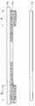
도 1은 본 발명의 바람직한 일실시예에 따른 테두리 라인을 표시하기 위한 액정 표시 장치의 개략도이다.1 is a schematic diagram of a liquid crystal display for displaying an edge line according to an exemplary embodiment of the present invention.
도 1을 참조하면, 본 발명의 바람직한 일실시예에 따른 테두리 라인을 표시 하기 위한 액정 표시 장치는 중앙 처리 장치(CPU)(10), 그래픽 제어부(20), 타이밍 제어부(30), 소스 구동부(40), 게이트 구동부(50) 및 LCD 패널(60)로 구성된다.Referring to FIG. 1, a liquid crystal display for displaying a border line according to an exemplary embodiment of the present invention includes a central processing unit (CPU) 10, a
예를 들어 중앙 처리 장치(10)로부터 입력된 제1 R.G.B. 신호는 그래픽 제어부(20) 및 타이밍 제어부(30)를 거치면서 테두리 라인 정보가 부가된 후 소스 구동부(40)에서 복수개의 데이터 라인(D1, D2, ..., Dm)을 통하여 액정 표시 패널(60)에 적절한 타이밍에 인가된다.For example, the first R.G.B. inputted from the
그래픽 제어부(20)는 중앙 처리 장치(10)로부터 제1 R.G.B. 신호를 입력받아 상기 제2 R.G.B. 신호, Vsync, Hsync, DE(Data Enable) 및 Mclk(Main clock)을 발생시켜 타이밍 제어부(30)에 제공한다. 제2 R.G.B. 신호는 제1 R.G.B. 신호와 동일한 색상 정보를 가진 R.G.B. 신호이다. Vsync는 입력된 R.G.B 신호를 근거로 디스플레이시 한 개의 프레임(frame)을 구별하기 위한 수직 동기 신호이고, Hsync는 각 프레임의 라인을 구별하기 위한 수평 동기 신호이다. DE는 화상 데이터가 출력되는 구간 동안만 하이(high) 레벨 상태를 유지하도록 하는 신호이고, Mclk는 메인 클럭 신호이다.The
타이밍 제어부(30)는 그래픽 제어부(20)로부터 제2 R.G.B. 신호, Hsync, Vsync, DE 및 Mclk 신호를 입력받아 이를 근거로 소스 구동부(40) 구동용 신호(LOAD, Hstart, 테두리 라인 정보를 포함한 R.G.B. 신호)와 게이트 구동부(50) 구동용 신호(게이트 clk, Vstart)를 출력한다.The
타이밍 제어부(30)는 예를 들어 표시 영역 중 첫째줄과 마지막 줄에 상응하는 테두리 라인을 나타내는 제1 더미 라인 신호 및 제2 더미 라인 신호를 발생시킨 다. 또한, 타이밍 제어부(30)는 입력된 제2 R.G.B. 신호에 예를 들어 표시 영역 중 좌측 및 우측 테두리 라인을 나타내는 데이터를 부가하여 테두리 라인 정보를 포함한 R.G.B 신호를 생성한다. 예를 들어, 상기 테두리 라인 데이터는 표시 영역의 각 테두리 라인에 대한 RGB 칼라 값을 가질 수 있다.The
Hstart는 타이밍 제어부(30)로부터 입력되는 테두리 라인 정보를 포함한 R.G.B. 신호등의 소스 구동부(40) 내로의 입력 시작을 나타내는 신호이다. LOAD 신호는 상기 소스 구동부(40)로 입력된 제1 더미 라인 신호, 제2 더미 라인 신호 및 테두리 라인 정보를 포함한 R.G.B. 신호가 소스 구동부(40)에서 아날로그 신호로 변환된 후 변환된 아날로그 신호를 액정 표시 패널(60)에 인가할 것을 명하는 신호이다.Hstart is an R.G.B. containing border line information input from the
LOAD 신호에 의해 제1 더미 라인 신호, 제2 더미 라인 신호 및 테두리 라인 정보를 포함한 R.G.B. 신호가 타이밍 제어부(30)의 제어하에 액정 표시 패널로 인가된다.R.G.B. including the first dummy line signal, the second dummy line signal and the edge line information by the LOAD signal. The signal is applied to the liquid crystal display panel under the control of the
소스 구동부(40)는 타이밍 제어부(30)로부터 입력된 소스 구동부(40) 구동용 신호(LOAD, Hstart, 테두리 라인 정보를 포함한 R.G.B. 신호)를 근거로 액정 표시 패널(60) 내의 액정을 구동시키는 데이터 라인 구동 신호 D1, D2, ..., Dm을 액정 표시 패널(60)의 데이터 라인에 각각 출력한다.The
게이트 구동부(50)는 타이밍 제어부(30)로부터 제공되는 게이트 구동부(50) 구동용 신호(게이트 clk, Vstart)를 근거로 액정 표시 패널(60) 내 박막 트랜지스터의 게이트 단자의 턴 온/턴 오프를 제어하기 위한 제1 더미 라인 구동 신호, 게 이트 라인 구동 신호 G1, G2, ..., Gn 및 제2 더미 라인 구동 신호를 액정 표시 패널(60)의 게이트 라인에 각각 출력한다. 게이트 clk는 제1 더미 라인 구동 신호, 복수의 게이트 라인 구동 신호 및 제2 더미 라인 구동 신호가 각각의 게이트 라인에 순차적으로 인가되도록 하는 클럭 신호이다. 이하, 제1 더미 라인 구동 신호, 복수의 게이트 라인 구동 신호 및 제2 더미 라인 구동 신호를 총괄하여 게이트 구동 신호라고도 한다. 예를 들어 사각 표시 영역을 가진 액정 표시 패널의 경우, 제1 및 제2 더미 라인 구동 신호는 상측, 하측 테두리 라인에 상응하는 액정 표시 패널(60)의 박막 트랜지스터들의 게이트 라인을 구동하기 위한 것이다.The gate driver 50 turns on / off the gate terminal of the thin film transistor in the liquid
Vstart 신호는 게이트 구동부(50)에서 액정 표시 패널(60) 내의 게이트 라인으로 입력되는 상기 게이트 구동 신호의 시작 시점을 나타내는 신호이다.The Vstart signal is a signal indicating a start time of the gate driving signal input from the gate driver 50 to the gate line in the liquid
LCD 패널(60)은 복수개의 게이트 라인(도시하지 않음), 상기 게이트 라인과 교차하는 복수 개의 데이터 라인(도시하지 않음), 박막 트랜지스터(도 5a, 도 6a 등 참조), 액정 커패시터(Clc, 도 5a 등 참조) 및 저장 커패시터(Cst)로 이루어진다.The
박막 트랜지스터는 상기 게이터 라인 및 데이터 라인으로 둘러싸인 영역에 매트릭스 형태로 배열되어 각각의 게이트 라인 및 데이터 라인에 연결된다. 액정 커패시터는 상기 박막 트랜지스터의 턴 온(turn on) 동작에 따라 상기 데이터 라인 구동 신호의 전압에 상응하여 광을 투과시킨다. 저장 커패시터는 박막 트랜지스터의 턴 온 시 데이터 라인 구동 신호의 전압을 축적하고, 박막 트랜지스터의 턴 오프(turn off)시 축적된 데이터 라인 구동 신호(D1, D2, ..., Dm)를 상기 액정 커패 시터에 인가한다.The thin film transistor is arranged in a matrix form in an area surrounded by the gator line and the data line, and is connected to each gate line and the data line. The liquid crystal capacitor transmits light corresponding to the voltage of the data line driving signal according to a turn on operation of the thin film transistor. The storage capacitor accumulates the voltage of the data line driving signal when the thin film transistor is turned on, and stores the data line driving signals D1, D2,..., Dm that are accumulated when the thin film transistor is turned off. Applied to the sheeter.
상기 설명한 테두리 라인을 디스플레이하기 위한 액정 표시 장치의 구동 회로는 액정 표시 장치에 한하여 적용되는 것은 아니고 약간의 변형을 통해 유기 EL(electroluminescent display) 등의 평판 패널 디스플레이 장치에도 그대로 적용이 가능하다.The driving circuit of the liquid crystal display device for displaying the edge lines described above is not limited to the liquid crystal display device but can be applied to a flat panel display device such as an organic electroluminescent display (EL) through a slight modification.
도 2는 도 1에 도시한 액정 표시 장치를 사용하여 액정 표시 패널에 테두리 라인이 디스플레이 되는 상태를 나타낸다.FIG. 2 illustrates a state in which an edge line is displayed on the liquid crystal display panel using the liquid crystal display shown in FIG. 1.
도 2를 참조하면, 액정 표시 패널(60)의 표시 영역(200)은 크게 테두리 라인들로 이루어지는 제1 영역과 상기 표시 영역(200) 중 테두리 라인을 제외한 제2 영역으로 나뉘어진다. 제1 영역은 표시 영역(200) 중 위쪽 테두리 라인을 나타내는 제1 테두리 영역(254a), 표시 영역(200)의 아래쪽 테두리 라인을 나타내는 제2 테두리 영역(254b), 표시 영역(200)의 좌측 테두리 라인을 나타내는 제3 테두리 영역(256-1, 256-2, ..., 256-n; 이하 256 이라고 한다) 및 표시 영역(200)의 우측 테두리 라인을 나타내는 제4 테두리 영역(258-1, 258-2, ..., 258-n; 이하 258 이라고 한다)으로 이루어진다.Referring to FIG. 2, the
제1 테두리 영역(254a)의 두께는 최소 1 픽셀(pixel) 이상이며, 사용자에 의해 상기 제1 테두리 영역(254a)의 두께가 자유롭게 설정할 수 있다. 즉, LCD 모듈의 세트 외부 일단에 제1 테두리 영역의 두께를 설정하도록 소정의 버튼을 장착할 수도 있고, LCD 디스플레이 화면상의 일단에 소정의 아이콘을 구비시키고 사용자가 아이콘을 누르는 경우에 원하는 두께를 지정하도록 할 수도 있다. 제2 내지 제4 테 두리 영역의 두께도 제1 테두리 영역과 동일한 두께를 가지거나 서로 다른 두께를 가지도록 조절이 가능하다.The thickness of the
상기 표시 영역(200) 중 테두리 라인을 제외한 제2 영역은 예를 들어, n 개의 라인으로 이루어진다.The second area of the
도 3은 도 1에 도시한 액정 표시 장치를 이용하여 테두리 라인을 표시하기 위하여 액정 표시 패널에 인가되는 R.G.B. 신호를 나타낸다.FIG. 3 is an R.G.B. applied to a liquid crystal display panel to display an edge line using the liquid crystal display shown in FIG. Indicates a signal.
도 3을 참조하면, 타이밍 제어부(30)에서 도 2에 도시된 표시 영역(200)의 제2 영역 중 첫 번째 라인, 두 번째 라인, ... , n 번째 라인에 디스플레이 되는 화상 데이터를 나타내는 첫 번째 라인 R.G.B. 신호(352-1), 두 번째 라인 R.G.B. 신호(352-2), ..., n 번째 라인 R.G.B. 신호(352-n)를 입력받는다. 여기서의 화상 데이터란 표시 영역에 디스플레이 되는 데이터 중 테두리 라인을 제외한 데이터를 나타낸다.Referring to FIG. 3, the
타이밍 제어부(30)에서는 제1 테두리 영역(254a)에 테두리 라인을 디스플레이 하기 위한 제1 더미 라인 신호 및 제2 테두리 영역(254b)에 테두리 라인을 디스플레이 하기 위한 제2 더미 라인 신호를 발생시킨다.The
또한, 타이밍 제어부(30)에서는 제3 테두리 영역(256)에 테두리 라인을 디스플레이 하기 위한 더미 픽셀 신호, 즉 첫 번째 라인 더미 픽셀 신호(356-1), 두 번째 라인 더미 픽셀 신호(356-2), ..., n 번째 라인 더미 픽셀 신호(356-n)(이하 제1 더미 픽셀 신호(356)이라고 한다)들을 상기 첫 번째 라인 R.G.B. 신호(352-1), 두 번째 라인 R.G.B. 신호(352-2), ..., n 번째 라인 R.G.B. 신호(352-n)의 일단에 각각 부가한다.In addition, the
또한, 타이밍 제어부(30)에서는 제4 테두리 영역(258)에 테두리 라인을 디스플레이 하기 위한 더미 픽셀 신호, 즉 첫 번째 라인 더미 픽셀 신호(358-1), 두 번째 라인 더미 픽셀 신호(358-2), ..., n 번째 라인 더미 픽셀 신호(358-n)(이하 제1 더미 픽셀 신호(358)이라고 한다)들을 상기 첫 번째 라인 R.G.B. 신호(352-1), 두 번째 라인 R.G.B. 신호(352-2), ..., n 번째 라인 R.G.B. 신호(352-n)의 타단에 각각 부가한다.In addition, the
즉, 타이밍 제어부(30)에서 상기 첫 번째 라인 R.G.B. 신호(352-1), 두 번째 라인 R.G.B. 신호(352-2), ..., n 번째 라인 R.G.B. 신호(352-n)에 테두리 라인을 표시하기 위한 제1 및 제2 더미 라인 신호, 복수의 더미 픽셀 신호를 부가시킴으로서 액정 표시 패널(60)에 테두리 라인을 디스플레이 할 수 있다.That is, the first line R.G.B. Signal 352-1, second line R.G.B. Signal 352-2, ..., n-th line R.G.B. The edge lines may be displayed on the liquid
이하, 소스 구동부(40)를 통하여 테두리 라인을 디스플레이하기 위하여 액정 표시 패널(60)로 화상 데이터가 인가되는 과정에 대해 설명한다.Hereinafter, a process of applying image data to the liquid
도 4는 도 1에 도시한 액정 표시 장치를 이용하여 테두리 라인을 표시하기 위하여 소스 구동부를 통하여 액정 표시 패널에 인가되는 R.G.B. 신호를 나타낸다.FIG. 4 is an R.G.B. applied to a liquid crystal display panel through a source driver to display an edge line using the liquid crystal display shown in FIG. Indicates a signal.
도 4를 참조하면, 먼저 게이트 구동부(50)로부터 제1 더미 라인 구동 신호가 액정 표시 패널(60)의 첫 번째 (row) 행에 속하는 각 게이트 라인에 인가되면, 첫 번째 행에 속하는 m 개의 데이터 라인에 각각 데이터 라인 구동 신호 D1, D2, ..., Dm의 첫 번째 행에 속하는 신호인 354-a-1, 354-a-2, 354-a-3, ..., 354-a-(m-2), 354-a-(m-1), 354-a-m이 출력된다. 그 결과, 도 2에 도시된 표시 영역(200)에 제1 테두리 라인이 디스플레이 된다.Referring to FIG. 4, when the first dummy line driving signal is first applied to each gate line belonging to the first row of the liquid
그 다음, 첫 번째 게이트 라인 구동 신호 G1이 액정 표시 패널(60)의 두번째 행에 속하는 각 게이트 라인에 인가되면, 두번째 행에 속하는 m 개의 데이터 라인에 각각 데이터 라인 구동 신호 D1, D2, ..., Dm의 두 번째 행에 속하는 신호인 356-1-1, 356-1-2, ..., 356-1-(m-1), 356-1-m이 출력된다. 그 결과, 도 2에 도시된 표시 영역(200)의 두 번째 행에 제3 및 제4 테두리 라인의 일부와 첫 번째 라인 R.G.B. 신호(352-1)가 디스플레이 된다.Then, when the first gate line driving signal G1 is applied to each gate line belonging to the second row of the liquid
두번째 게이트 라인 구동 신호 G2가 액정 표시 패널(60)의 세번째 행에 속하는 각 게이트 라인에 인가되면, 세번째 행에 속하는 m 개의 데이터 라인에 각각 데이터 라인 구동 신호 D1, D2, ..., Dm의 세번째 행에 속하는 신호인 356-2-1, 356-2-2, ..., 356-2-(m-1), 356-2-m이 출력된다. 그 결과, 도 2에 도시된 표시 영역(200)의 세번째 행에 제3 및 제4 테두리 라인의 일부와 두번째 라인 R.G.B. 신호(352-2)가 디스플레이 된다.When the second gate line driving signal G2 is applied to each gate line belonging to the third row of the liquid
이상과 같은 방법으로 네 번째 행, 다섯 번째 행, ..., n-2 번째 행까지 디스플레이가 수행된다. 그 다음, n 번째 게이트 라인 구동 신호 Gn가 액정 표시 패널(60)의 n+1 번째 행에 속하는 각 게이트 라인에 인가되면, n+1 번째 행에 속하는 m 개의 데이터 라인에 각각 데이터 라인 구동 신호 D1, D2, ..., Dm의 n+1 번째 행에 속하는 신호인 356-n-1, 356-n-2, ..., 356-n-(m-1), 356-n-m이 출력된다. 그 결과, 도 2에 도시된 표시 영역(200)의 n+1 번째 행에 제3 및 제4 테두리 라인의 일부와 n번째 라인 R.G.B. 신호(352-n)가 디스플레이 된다.In the same manner as described above, the display is performed up to the fourth row, the fifth row, ..., n-2th row. Then, when the n-th gate line driving signal Gn is applied to each gate line belonging to the n + 1th row of the liquid
마지막으로, 제2 더미 라인 구동 신호가 액정 표시 패널(60)의 n+2 번째 행에 속하는 각 게이트 라인에 인가되면, n=2 번째 행에 속하는 m 개의 데이터 라인에 각각 데이터 라인 구동 신호 D1, D2, ..., Dm의 n+2 번째 행에 속하는 신호인 354-b-1, 354-b-2, 354-b-3, ..., 354-b-(m-2), 354-b-(m-1), 354-b-m이 출력된다. 그 결과, 도 2에 도시된 표시 영역(200)에 제2 테두리 라인이 디스플레이 된다. 이상은 액정 표시 패널(60) 구동 회로 중 타이밍 제어부(30)의 더미 라인 신호 및 더미 픽셀 신호등의 제어 신호를 이용하여 테두리 라인을 구하는 방법을 설명하였다. 이 경우는 타이밍 제어부(30)에서 별도로 더미 라인 신호 및 더미 픽셀 신호등을 발생시켜야 한다.Finally, when the second dummy line driving signal is applied to each gate line belonging to the n + 2th row of the liquid
이하에서는 액정 표시 패널(60)의 칼라 필터와 노멀리 화이트(normally white) 모드에서의 액정을 이용하여 테두리 라인을 구현하는 방법을 설명한다.Hereinafter, a method of implementing the edge line using the color filter of the liquid
노멀리 화이트(normally white) 모드란 액정 표시 패널(60)의 박막 트랜지스터 기판과 칼라 필터 기판 사이에 개재된 액정 층으로 입사된 빛이 전부 투과되는 상태를 말한다. 노멀리 화이트(normally white) 모드를 구현하기 위해서는 액정층에 전계가 인가되지 않도록 함으로써 액정층을 통하여 모든 빛이 투과되도록 한다. 즉, 액정층에 무전계(無電界)를 형성한다.The normally white mode refers to a state in which all light incident on the liquid crystal layer interposed between the thin film transistor substrate and the color filter substrate of the liquid
액정 표시 패널(60)의 테두리에 영역에 해당되는 칼라 필터 기판 부분에 색화소를 형성하고 노멀리 화이트(normally white) 상태에서 테두리 영역에 해당되는 화소 전극(pixel electrode) 들에는 신호가 인가되지 않도록 함으로써 소정의 색을 가지는 테두리 라인을 구현할 수 있다.Color pixels are formed on a portion of the color filter substrate corresponding to the area of the edge of the liquid
테두리 영역에 해당되는 픽셀(pixel)들에는 신호가 인가되지 않도록 하는 방 법으로는 테두리 라인에 상응하는 박막 트랜지스터 기판 부분에 박막 트랜지스터를 형성하지 않는 방법, 테두리 라인에 상응하는 박막 트랜지스터 기판 부분에 형성된 박막 트랜지스터와 화소 전극간의 전기적 연결을 차단하는 방법 등이 있다.As a method of preventing a signal from being applied to pixels corresponding to the edge area, a method of not forming a thin film transistor in a portion of a thin film transistor substrate corresponding to the edge line, or a portion of the thin film transistor substrate portion corresponding to the edge line And a method of blocking electrical connection between the thin film transistor and the pixel electrode.
테두리 영역에 해당되는 부분에 픽셀 불량이 발생할 경우 상기 불량 픽셀들은 노멀리 화이트 모드가 형성될 수 있다. 즉, 사진 식각 공정에서 발생되는 이물질에 의해 패턴이 형성되지 않거나, 이물질에 의해 콘택부간의 연결이 안 되는 경우 등에는 박막 트랜지스터의 소스 전극으로부터 픽셀로 신호가 인가되지 않게 된다. 본 발명에서는 이러한 픽셀 불량 현상을 테두리 라인을 구현하는데 이용할 수 있다. 즉, 테두리 라인에 해당되는 픽셀부에 픽셀 불량 현상이 발생할 경우에도 테두리 라인을 구현하는데는 아무런 문제가 없으므로 공정 불량 발생에 대해 강하게 된다.When a pixel defect occurs in a portion corresponding to an edge region, the defective pixels may be normally white mode. That is, when the pattern is not formed by the foreign material generated in the photolithography process or when the contact between the contact parts is not formed by the foreign material, the signal is not applied to the pixel from the source electrode of the thin film transistor. In the present invention, such a pixel defect phenomenon may be used to implement a border line. That is, even when the pixel defect phenomenon occurs in the pixel portion corresponding to the border line, there is no problem in implementing the border line.
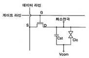
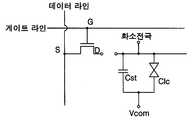
도 5a 내지 도 5c는 본 발명에 따른 테두리 라인을 표시하기 위하여 액정 표시 패널의 테두리 라인에 상응하는 박막 트랜지스터의 등가 회로도이고, 도 6a 내지 도 6c는 도 5a 내지 도 5c의 박막 트랜지스터를 구현한 액정 표시 패널의 단면도이다. 특히 도 6a 내지 6c는 게이트(top gate) 방식의 박막 트랜지스터를 나타낸 것이다.5A to 5C are equivalent circuit diagrams of thin film transistors corresponding to edge lines of a liquid crystal display panel to display edge lines according to the present invention, and FIGS. 6A to 6C are liquid crystals implementing the thin film transistors of FIGS. 5A to 5C. It is sectional drawing of a display panel. In particular, FIGS. 6A to 6C illustrate a thin film transistor of a top gate type.
도 5a 및 6a를 참조하면, 액정 표시 패널(60)에 형성된 게이트 라인은 박막 트랜지스터의 게이트 단자에 연결되고, 데이터 라인은 박막 트랜지스터의 소스 단자에 연결된다.5A and 6A, a gate line formed in the liquid
액정 층(120)은 화소 전극(112)과 전기적으로 연결된 박막 트랜지스터의 드 레인(Drain) 전극(108)에 일단이 연결되고, 타단이 칼라 필터 기판(170)의 공통 전극(176)에 연결되어 액정 커패시터(Clc)를 형성한다. 액정 커패시터는 상기 박막 트랜지스터의 턴 온(turn on) 동작에 따라 상기 드레인 전극(108)을 통해 입력되는 데이터 라인 구동 신호의 전압에 상응하여 액정 층(120)에 입사된 광을 투과시킨다.The
저장 커패시터(Cst)는 액정 커패시터에 병렬로 연결되며, 박막 트랜지스터의 턴 온 시 데이터 라인 구동 신호의 전압을 축적하여 박막 트랜지스터의 턴 오프(turn off)시 축적된 데이터 라인 구동 신호(D1, D2, ..., Dm)를 상기 액정 커패시터에 인가한다.The storage capacitor Cst is connected in parallel to the liquid crystal capacitor and accumulates the voltage of the data line driving signal when the thin film transistor is turned on, and thus the data line driving signals D1, D2, ..., Dm) is applied to the liquid crystal capacitor.
도 6a에 도시된 바와 같이, 박막 트랜지스터 기판(110)에는 채널층(104)의 상부에 게이트 전극(106)이 형성되고, 게이트 전극(106) 위에 드레인 전극(108)과 소스 전극(102)이 형성된다. 소스 전극(102)은 채널층(104)을 통하여 드레인 전극(108)과 전기적으로 연결된다. 드레인 전극(108)이 형성된 후, 화소 전극(112)이 형성되며, 화소 전극(112)은 드레인 전극(108)과 일부분이 전기적으로 연결된다.As shown in FIG. 6A, a
칼라 필터 기판(170)에는 투명 기판(172) 상에 상기 화소 전극(112)에 대향하도록 색화소(174)가 형성되고, 색화소(174) 상에 공통 전극(176)이 형성된다. 소스 구동부(40)를 통하여 입력된 데이터 라인 구동 신호는 소오스 전극(102), 드레인 전극(108)을 거쳐 화소 전극(112)에 인가된다. 공통 전극(176)에 소정의 전압이 인가된 상태에서 액정 층(120) 내의 각각의 액정 분자는 상기 공통 전극(176)과 화소 전극(112)간에 형성된 전계의 방향에 따라 재배열된다. 상기 전계의 세기에 따라 액정 분자의 재배열의 정도가 변하여 액정을 투과하는 광의 양이 달라지며, 액정 층(120)을 통과한 광은 색화소(174)를 통과하면서 상기 색화소(174)의 R.G.B. 값에 상응하는 색을 나타낸다.A
테두리 영역에 해당되는 픽셀(pixel)들에 신호가 인가되지 않도록 하는 방법 중 하나는 테두리 라인에 상응하는 픽셀에 속하는 박막 트랜지스터(114)와 화소 전극(112) 간의 전기적 연결을 차단하는 것이다.One method of preventing a signal from being applied to pixels corresponding to the edge area is to cut off an electrical connection between the
첫 번째 방법으로 테두리 영역에 상응하는 픽셀에 속하는 박막 트랜지스터(114)의 게이트 단자를 게이트 라인과 연결하지 않고 그라운드와 연결하여 항상 박막 트랜지스터(114)를 턴 오프 상태로 유지하도록 하여 데이터 라인을 통하여 입력되는 화상 데이터가 화소 전극(112)으로 전달되지 않도록 한다. 또한, 화소 전극(112)과 공통 전극(176)을 전기적으로 연결시켜 전위차가 0이 되도록 하여 노멀리 화이트 모드를 유지하면 액정을 통과한 광이 칼라 필터 기판(170)에 형성된 색화소(174)를 거치면서 테두리 라인에 소정의 색이 구현된다.In the first method, the gate terminal of the
두 번째 방법은 도 5b에 도시한 바와 같이, 화소 전극(112)과 공통 전극(176)간에 전위차를 0으로 유지하고, 테두리 라인에 상응하는 픽셀에 속하는 박막 트랜지스터(114)의 드레인 단자를 오픈(open)시키는 것이다. 그 결과, 데이터 라인을 통하여 입력되는 화상 데이터가 화소 전극(112)으로 전달되지 않게 되어 노멀리 화이트 모드에서 액정을 투과한 광이 칼라 필터 기판(170)에 형성된 색화소(174)를 거치면서 테두리 라인에 소정의 색이 구현된다.The second method maintains the potential difference between the
이러한 드레인 단자를 오픈 시킨 경우의 액정 표시 패널(60)의 단면도를 나타낸 것이 도 6b이다.6B is a cross-sectional view of the liquid
도 6b를 참조하면, 드레인 단자를 오픈시키기 위해 드레인 전극(108)이 화소 전극(112)이 서로 접촉되지 않도록 형성한다.Referring to FIG. 6B, the
세 번째 방법은 도 5c에 도시한 바와 같이, 화소 전극(112)과 공통 전극(176)간에 전위차를 0으로 유지하고, 테두리 라인에 상응하는 픽셀에 속하는 박막 트랜지스터(114)를 박막 트랜지스터 기판(110)에 형성하지 않는 것이다. 그 결과, 데이터 라인을 통하여 입력되는 화상 데이터가 화소 전극(112)으로 전달되지 않게 되어 노멀리 화이트 모드에서 액정을 투과한 광이 칼라 필터 기판(170)에 형성된 색화소(174)를 거치면서 테두리 라인에 소정의 색이 구현된다.In the third method, as shown in FIG. 5C, the potential difference between the
이러한 박막 트랜지스터(114)를 제거한 경우의 액정 표시 패널(60)의 단면도를 나타낸 것이 도 6c이다. 한편, 박막 트랜지스터(114) 뿐만 아니라 화소 전극(112) 자체도 제거하여 박막 트랜지스터 기판(110)에 형성하지 않을 수도 있다.6C is a cross-sectional view of the liquid
네번째 방법은 별도의 마스크를 사용하여 칼라 필터 기판(170) 중 테두리 영역에 상응하는 부분에 형성된 공통 전극(176) 부분을 제거하는 것이다. 이와 같이 테두리 영역에 상응하는 액정 층의 양단에 전계가 인가되지 않도록 함으로써 테두리 라인에 소정의 색을 디스플레이 할 수 있다.The fourth method is to remove the portion of the
도 7은 테두리 라인을 표시하기 위하여 액정 표시 패널에 색화소를 형성할 경우 본 발명의 바람직한 제1 실시예에 따른 색화소가 형성된 액정 표시 패널의 개 략도이다.7 is a schematic diagram of a liquid crystal display panel in which a color pixel according to the first exemplary embodiment of the present invention is formed when color pixels are formed in the liquid crystal display panel to display an edge line.
도 7을 참조하면, 청색(blue)의 테두리 라인을 형성하기 위한 색화소(B)가 칼라 필터 기판(170)의 테두리 영역에 상응하는 부분인 B1, B1'에 형성된다. 도 7과 같이 1개 층의 색화소를 사용하여 원하는 색깔의 테두리를 디스플레이 할 수 있다.Referring to FIG. 7, a color pixel B for forming a blue border line is formed in B1 and B1 ′, which are portions corresponding to the edge region of the
즉, 위에서 상술한 방법에 따라 노멀리 화이트 모드에서 테두리 영역에 해당되는 픽셀(pixel)들에 신호가 인가되지 않도록 하면, 테두리 라인에 상응하는 부분의 액정을 투과한 광이 색화소(B)를 거치면서 청색의 테두리 라인이 디스플레이 된다.That is, when the signal is not applied to the pixels corresponding to the edge area in the normally white mode according to the above-described method, the light passing through the liquid crystal of the portion corresponding to the edge line is colored with the color pixel B. FIG. As you go through, a blue border line is displayed.
도 7은 테두리 라인을 표시하기 위하여 액정 표시 패널에 색화소를 형성할 경우 본 발명의 바람직한 제1 실시예에 따른 색화소가 형성된 액정 표시 패널의 개략도이다.7 is a schematic diagram of a liquid crystal display panel in which a color pixel according to the first exemplary embodiment of the present invention is formed when color pixels are formed in the liquid crystal display panel to display edge lines.
도 8은 테두리 라인을 표시하기 위하여 액정 표시 패널에 색화소를 형성할 경우 본 발명의 바람직한 제2 실시예에 따른 색화소가 형성된 액정 표시 패널의 개략도이고, 도 9는 테두리 라인을 표시하기 위하여 액정 표시 패널에 색화소를 형성할 경우 본 발명의 바람직한 제3 실시예에 따른 색화소가 형성된 액정 표시 패널의 개략도이다.8 is a schematic diagram of a liquid crystal display panel in which a color pixel is formed according to a second exemplary embodiment of the present invention when a color pixel is formed in a liquid crystal display panel to display an edge line, and FIG. 9 is a liquid crystal display to display an edge line. When the color pixels are formed in the display panel, a schematic view of the liquid crystal display panel in which the color pixels according to the third exemplary embodiment of the present invention are formed is shown.
도 8 및 도 9를 참조하면, 소정 색깔의 테두리 라인을 형성하기 위하여 R, G, B의 색화소 층이 칼라 필터 기판(170)의 테두리 영역에 상응하는 부분인 B1, B1'에 형성된다.8 and 9, in order to form a border line of a predetermined color, a color layer of R, G, and B is formed on B1 and B1 ′, which are portions corresponding to the border region of the
도 8은 레드(R), 그린(G), 블루(B)가 교대로 배치된 1개 층의 색화소를 사용하여 흰색의 테두리를 디스플레이 하는 경우를 나타낸다.FIG. 8 shows a case where a white border is displayed using one layer of color pixels in which red (R), green (G), and blue (B) are alternately arranged.
한편, 도 9와 같이 각각의 색화소 층의 두께 T1, T2, T3은 서로 다를 수도 있고, 또는 서로 같을 수도 있다. 즉, 도 9와 같이 색화소의 두께를 조절하여 원하는 색깔의 테두리 라인을 형성할 수도 있다. 스핀 코딩(spin coating) 또는 슬릿 코터(slit coater)를 이용한 코팅시 색화소의 코팅 두께를 다르게 하거나 슬릿 마스크를 사용한 슬릿 노광 등의 방법을 통하여 색화소의 두께를 조절할 수 있다.Meanwhile, as illustrated in FIG. 9, the thicknesses T1, T2, and T3 of each color layer may be different from each other, or may be the same as each other. That is, as shown in FIG. 9, the thickness of the color pixel may be adjusted to form a border line of a desired color. The thickness of the color pixel may be controlled by a method such as changing the coating thickness of the color pixel when coating by spin coating or a slit coater or by using a slit mask using a slit mask.
즉, 위에서 상술한 방법에 따라 노멀리 화이트 모드에서 테두리 영역에 해당되는 픽셀(pixel)들에 신호가 인가되지 않도록 하면, 테두리 라인에 상응하는 부분의 액정을 투과한 광이 R, G, B의 색화소를 거치면서 흰색 또는 흰색 외의 다른 색깔의 테두리 라인이 디스플레이 된다.That is, when the signal is not applied to the pixels corresponding to the edge region in the normally white mode according to the above-described method, the light transmitted through the liquid crystal of the portion corresponding to the edge line is R, G, B. As you go through the color pixels, a border line of white or any other color other than white is displayed.
도 10은 테두리 라인을 표시하기 위하여 액정 표시 패널에 색화소를 형성할 경우 본 발명의 바람직한 제4 실시예에 따른 색화소가 형성된 액정 표시 패널의 개략도이다.10 is a schematic view of a liquid crystal display panel in which a color pixel according to a fourth exemplary embodiment of the present invention is formed when color pixels are formed in the liquid crystal display panel to display edge lines.
도 10을 참조하면, 소정 색깔의 테두리 라인을 형성하기 위하여 R, B의 2개 층의 색화소 층이 칼라 필터 기판(170)의 테두리 영역에 상응하는 부분인 B1, B1'에 형성된다. 즉, 도 10은 2개 층의 색화소를 사용하여 소정 색깔의 테두리를 디스플레이 하는 경우를 나타낸다.Referring to FIG. 10, two color pixel layers of R and B are formed in B1 and B1 ′ corresponding to the edge region of the
2개 층의 색화소를 사용하는 경우에도 각각의 색화소 층의 두께는 동일하거나 서로 다르게 할 수 있다.Even when two color pixels are used, the thickness of each color layer may be the same or different.
도 11은 테두리 라인을 표시하기 위하여 액정 표시 패널에 색화소를 형성할 경우 본 발명의 바람직한 제5 실시예에 따른 색화소가 형성된 액정 표시 패널의 개략도이다.FIG. 11 is a schematic diagram of a liquid crystal display panel in which a color pixel according to a fifth exemplary embodiment of the present invention is formed when color pixels are formed in a liquid crystal display panel to display an edge line.
도 11을 참조하면, 2가지 색깔의 테두리 라인을 형성하기 위하여 3개 층의 색화소 층이 칼라 필터 기판(170)의 테두리 영역에 상응하는 부분인 B1, B1'에 형성된다. 즉, 도 11은 3개 층의 색화소를 사용하여 2가지 색깔의 테두리를 디스플레이 하는 경우를 나타낸다. 이 때, 각각의 색화소 층의 두께는 동일하거나 서로 다르게 할 수 있다. 도 11에 의하면 적색(R)과 각 색화소 층의 두께를 조절함으로써 적색이외의 소정의 색깔을 가지는 2가지 색깔의 테두리 라인의 디스플레이가 가능하다. 이 외에도 2가지 색깔의 테두리 라인은 1개 층의 색화소 층을 형성하여 구현할 수도 있고, 2개 층의 색화소 층을 형성하여 구현할 수도 있다.Referring to FIG. 11, three layers of color pixels are formed in B1 and B1 ′, which correspond to edge regions of the
본 발명에 따르는 테두리 라인을 디스플레이 하는 방법의 기본적인 기술적 사상은 액정 표시 장치에 한하여 적용되는 것은 아니고, 유기 EL(electroluminescent display), 플라즈마 디스플레이 패널(Plasma Display Panel), FED(Field Emission display) 등의 기타 평판 패널 디스플레이 장치에도 적용이 가능하다.The basic technical idea of the method for displaying the edge line according to the present invention is not limited to a liquid crystal display device, but may be applied to an organic electroluminescent display (EL), a plasma display panel, a field emission display, and the like. It is also applicable to flat panel display devices.
실시예를 참조하여 설명하였지만, 해당 기술 분야의 숙련된 당업자는 하기의 특허 청구의 범위에 기재된 본 발명의 사상 및 영역으로부터 벗어나지 않는 범위 내에서 본 발명을 다양하게 수정 및 변경시킬 수 있음을 이해할 수 있을 것이다.
Although described with reference to the examples, those skilled in the art can understand that the present invention can be variously modified and changed without departing from the spirit and scope of the invention described in the claims below. There will be.
이상, 설명한 바와 같이 본 발명에서는 액정 표시 패널의 구동 방법을 이용함으로써 액티브 매트릭스 방식의 화면 표시 장치에 대하여 사용자가 직접 원하는 색깔을 설정하여 소정 색깔의 테두리 라인을 디스플레이 할 수 있다.As described above, in the present invention, by using the driving method of the liquid crystal display panel, the user may directly set a desired color for the active matrix display device and display a border line of a predetermined color.
또한, 노멀리 화이트 모드(normally white mode)하에서 테두리 라인에 상응하는 부분에 다양한 패턴의 색화소 층을 형성함으로써 액티브 매트릭스 방식의 화면 표시 장치에 대하여 다양한 색깔의 테두리 라인을 디스플레이할 수 있다.In addition, various color border lines may be displayed on an active matrix display device by forming a color layer of various patterns in a portion corresponding to the border line in a normally white mode.
또한, 기존의 박막 트랜지스터 제조 공정에서 테두리 라인에 해당되는 픽셀부에 픽셀 불량 현상이 발생할 경우에도 소정 색깔의 테두리 라인을 구현할 수 있는 효과가 있다.In addition, in the conventional thin film transistor manufacturing process, even when a pixel defect occurs in the pixel portion corresponding to the edge line, the edge line of a predetermined color may be realized.
또한, 테두리 라인을 디스플레이 함으로써 표시 영역의 외곽 테두리와 실제 영상 이미지간에 명확한 구분을 주어 액자와 같은 분위기를 액티브 매트릭스 구동 방식의 화면 표시 장치에서 구현할 수 있다.
In addition, by displaying a border line, a distinction between an outer border of a display area and an actual video image may be provided to implement an atmosphere such as a frame in an active matrix driving screen display device.
Claims (24)
Translated fromKoreanPriority Applications (10)
| Application Number | Priority Date | Filing Date | Title |
|---|---|---|---|
| KR1020020053635AKR100878790B1 (en) | 2002-09-05 | 2002-09-05 | Active matrix image display device and image display method using same |
| AU2003253464AAU2003253464A1 (en) | 2002-09-05 | 2003-08-26 | Active matrix driving display device and image displaying method using the same |
| CNB038208628ACN100476533C (en) | 2002-09-05 | 2003-08-26 | Active matrix drive display and image display method using same |
| PCT/KR2003/001719WO2004023191A2 (en) | 2002-09-05 | 2003-08-26 | Active matrix driving display device and image displaying method using the same |
| US10/526,689US7894021B2 (en) | 2002-09-05 | 2003-08-26 | Active matrix driving display device and image displaying method using the same wherein a thin film transistor corresponding to a border area is turned off |
| TW092124587ATWI425483B (en) | 2002-09-05 | 2003-09-05 | Active matrix driving display device and image displaying method using the same |
| TW102133627ATWI460710B (en) | 2002-09-05 | 2003-09-05 | Active matrix driving display device and image displaying method using the same |
| US13/016,416US8218112B2 (en) | 2002-09-05 | 2011-01-28 | Active matrix driving display device and image displaying method using the same |
| US13/474,762US8947609B2 (en) | 2002-09-05 | 2012-05-18 | Active matrix driving display device and image displaying method using the same |
| US14/610,209US9454050B2 (en) | 2002-09-05 | 2015-01-30 | Active matrix driving display device and image displaying method using the same |
Applications Claiming Priority (1)
| Application Number | Priority Date | Filing Date | Title |
|---|---|---|---|
| KR1020020053635AKR100878790B1 (en) | 2002-09-05 | 2002-09-05 | Active matrix image display device and image display method using same |
Publications (2)
| Publication Number | Publication Date |
|---|---|
| KR20040022359A KR20040022359A (en) | 2004-03-12 |
| KR100878790B1true KR100878790B1 (en) | 2009-01-14 |
Family
ID=31973665
Family Applications (1)
| Application Number | Title | Priority Date | Filing Date |
|---|---|---|---|
| KR1020020053635AExpired - LifetimeKR100878790B1 (en) | 2002-09-05 | 2002-09-05 | Active matrix image display device and image display method using same |
Country Status (6)
| Country | Link |
|---|---|
| US (4) | US7894021B2 (en) |
| KR (1) | KR100878790B1 (en) |
| CN (1) | CN100476533C (en) |
| AU (1) | AU2003253464A1 (en) |
| TW (2) | TWI460710B (en) |
| WO (1) | WO2004023191A2 (en) |
Families Citing this family (20)
| Publication number | Priority date | Publication date | Assignee | Title |
|---|---|---|---|---|
| KR101158868B1 (en)* | 2005-06-29 | 2012-06-25 | 엘지디스플레이 주식회사 | Liquid Crystal Display capable of adjusting each brightness level in plural divided areas and method for driving the same |
| TWI326379B (en)* | 2005-09-20 | 2010-06-21 | Au Optronics Corp | A double-sided liquid crystal display |
| KR100761296B1 (en) | 2006-03-17 | 2007-09-27 | 엘지전자 주식회사 | Light emitting device and method for driving same |
| KR100740133B1 (en)* | 2006-07-31 | 2007-07-16 | 삼성에스디아이 주식회사 | Light emitting display |
| KR101543280B1 (en)* | 2009-02-16 | 2015-08-11 | 삼성디스플레이 주식회사 | Display panel and display apparatus having the display panel |
| US8456586B2 (en) | 2009-06-11 | 2013-06-04 | Apple Inc. | Portable computer display structures |
| US8408780B2 (en) | 2009-11-03 | 2013-04-02 | Apple Inc. | Portable computer housing with integral display |
| US8743309B2 (en) | 2009-11-10 | 2014-06-03 | Apple Inc. | Methods for fabricating display structures |
| US8467177B2 (en) | 2010-10-29 | 2013-06-18 | Apple Inc. | Displays with polarizer windows and opaque masking layers for electronic devices |
| US9143668B2 (en) | 2010-10-29 | 2015-09-22 | Apple Inc. | Camera lens structures and display structures for electronic devices |
| KR101749161B1 (en)* | 2010-12-29 | 2017-06-21 | 삼성디스플레이 주식회사 | Display panel and display device having the same |
| JP6004560B2 (en)* | 2011-10-06 | 2016-10-12 | 株式会社ジャパンディスプレイ | Display device |
| US9488891B2 (en)* | 2013-04-22 | 2016-11-08 | National University Of Singapore | Thin-surface liquid crystal based voltage sensor |
| KR102305456B1 (en)* | 2014-12-02 | 2021-09-28 | 삼성디스플레이 주식회사 | Display apparatus and method of driving the same |
| CN105741748B (en)* | 2016-03-04 | 2019-05-14 | 京东方科技集团股份有限公司 | A kind of display panel, display equipment and production method |
| KR102449200B1 (en)* | 2017-07-04 | 2022-09-30 | 삼성디스플레이 주식회사 | Display device including clock wiring |
| US11637919B2 (en) | 2019-12-03 | 2023-04-25 | Apple Inc. | Handheld electronic device |
| US11838432B2 (en) | 2019-12-03 | 2023-12-05 | Apple Inc. | Handheld electronic device |
| US12003657B2 (en) | 2021-03-02 | 2024-06-04 | Apple Inc. | Handheld electronic device |
| US12267449B2 (en) | 2022-03-03 | 2025-04-01 | Apple Inc. | Handheld electronic device |
Citations (2)
| Publication number | Priority date | Publication date | Assignee | Title |
|---|---|---|---|---|
| JPH10187099A (en)* | 1996-12-24 | 1998-07-14 | Casio Comput Co Ltd | LCD drive method |
| EP1022604A2 (en)* | 1992-02-27 | 2000-07-26 | Canon Kabushiki Kaisha | Liquid crystal display device |
Family Cites Families (18)
| Publication number | Priority date | Publication date | Assignee | Title |
|---|---|---|---|---|
| JPS576882A (en)* | 1980-06-16 | 1982-01-13 | Hitachi Ltd | Liquid crystal display element |
| US4917471A (en)* | 1986-08-30 | 1990-04-17 | Canon Kabushiki Kaisha | Liquid crystal device |
| US5365357A (en)* | 1988-04-21 | 1994-11-15 | Asahi Glass Company Ltd. | Color liquid crystal display having color filters and light blocking layers in the periphery |
| KR960014823B1 (en)* | 1991-03-15 | 1996-10-21 | 가부시기가이샤 히다찌세이사구쇼 | LCD Display |
| JP3299869B2 (en)* | 1995-09-27 | 2002-07-08 | シャープ株式会社 | Liquid crystal display device and manufacturing method thereof |
| US5907379A (en)* | 1996-10-21 | 1999-05-25 | Samsung Electronics Co., Ltd. | In-plane switching liquid crystal display having high aperture ratio |
| TW520457B (en)* | 1997-09-30 | 2003-02-11 | Toshiba Corp | Display panel and position adjusting method for the display panel |
| GB9825314D0 (en)* | 1998-11-20 | 1999-01-13 | Koninkl Philips Electronics Nv | Active matrix liquid crystal display devices |
| WO2001057838A1 (en)* | 2000-01-31 | 2001-08-09 | Seiko Epson Corporation | Electrooptic device and driving method thereof |
| JP3652997B2 (en)* | 2000-06-14 | 2005-05-25 | Nec液晶テクノロジー株式会社 | Liquid crystal material and liquid crystal display device |
| JP3516441B2 (en)* | 2000-07-10 | 2004-04-05 | インターナショナル・ビジネス・マシーンズ・コーポレーション | Active matrix substrate, display device, and method of manufacturing active matrix substrate |
| KR100604271B1 (en)* | 2000-10-16 | 2006-07-24 | 엘지.필립스 엘시디 주식회사 | Liquid crystal display |
| US6961029B1 (en)* | 2000-11-08 | 2005-11-01 | Palm, Inc. | Pixel border for improved viewability of a display device |
| KR100729762B1 (en)* | 2000-11-14 | 2007-06-20 | 삼성전자주식회사 | Liquid crystal display with improved side contrast ratio and side color reproducibility |
| JP3698208B2 (en)* | 2001-12-06 | 2005-09-21 | セイコーエプソン株式会社 | Electro-optical device and electronic apparatus |
| JP2003295207A (en)* | 2002-03-29 | 2003-10-15 | Nec Lcd Technologies Ltd | In-plane switching type active matrix liquid crystal display |
| JP4036081B2 (en)* | 2002-11-12 | 2008-01-23 | セイコーエプソン株式会社 | Electro-optical panel and manufacturing method thereof |
| JP3800184B2 (en)* | 2003-02-04 | 2006-07-26 | セイコーエプソン株式会社 | Electro-optical device and electronic apparatus |
- 2002
- 2002-09-05KRKR1020020053635Apatent/KR100878790B1/ennot_activeExpired - Lifetime
- 2003
- 2003-08-26WOPCT/KR2003/001719patent/WO2004023191A2/ennot_activeCeased
- 2003-08-26CNCNB038208628Apatent/CN100476533C/ennot_activeExpired - Lifetime
- 2003-08-26USUS10/526,689patent/US7894021B2/enactiveActive
- 2003-08-26AUAU2003253464Apatent/AU2003253464A1/ennot_activeAbandoned
- 2003-09-05TWTW102133627Apatent/TWI460710B/ennot_activeIP Right Cessation
- 2003-09-05TWTW092124587Apatent/TWI425483B/ennot_activeIP Right Cessation
- 2011
- 2011-01-28USUS13/016,416patent/US8218112B2/ennot_activeExpired - Fee Related
- 2012
- 2012-05-18USUS13/474,762patent/US8947609B2/ennot_activeExpired - Lifetime
- 2015
- 2015-01-30USUS14/610,209patent/US9454050B2/ennot_activeExpired - Fee Related
Patent Citations (3)
| Publication number | Priority date | Publication date | Assignee | Title |
|---|---|---|---|---|
| EP1022604A2 (en)* | 1992-02-27 | 2000-07-26 | Canon Kabushiki Kaisha | Liquid crystal display device |
| EP1022604B1 (en)* | 1992-02-27 | 2003-09-03 | Canon Kabushiki Kaisha | Liquid crystal display device |
| JPH10187099A (en)* | 1996-12-24 | 1998-07-14 | Casio Comput Co Ltd | LCD drive method |
Also Published As
| Publication number | Publication date |
|---|---|
| US20060050205A1 (en) | 2006-03-09 |
| US20110134376A1 (en) | 2011-06-09 |
| CN1678950A (en) | 2005-10-05 |
| TWI460710B (en) | 2014-11-11 |
| US9454050B2 (en) | 2016-09-27 |
| KR20040022359A (en) | 2004-03-12 |
| US20150138468A1 (en) | 2015-05-21 |
| TW201403578A (en) | 2014-01-16 |
| TWI425483B (en) | 2014-02-01 |
| US20120229530A1 (en) | 2012-09-13 |
| WO2004023191A2 (en) | 2004-03-18 |
| AU2003253464A8 (en) | 2004-03-29 |
| US7894021B2 (en) | 2011-02-22 |
| WO2004023191A3 (en) | 2004-06-24 |
| TW200409079A (en) | 2004-06-01 |
| CN100476533C (en) | 2009-04-08 |
| US8218112B2 (en) | 2012-07-10 |
| AU2003253464A1 (en) | 2004-03-29 |
| US8947609B2 (en) | 2015-02-03 |
Similar Documents
| Publication | Publication Date | Title |
|---|---|---|
| KR100878790B1 (en) | Active matrix image display device and image display method using same | |
| US10229645B2 (en) | Display device and electronic apparatus | |
| KR101005654B1 (en) | Display device | |
| US20110001910A1 (en) | Liquid crystal display device | |
| US8482686B2 (en) | Displays with minimized crosstalk | |
| CN100405605C (en) | Active Device Matrix Substrate | |
| KR20090091028A (en) | Electro-optical devices and electronic devices | |
| WO2016131224A1 (en) | Display device and drive method thereof | |
| KR20120004119A (en) | LCD Display | |
| JP4491632B2 (en) | Driving method of liquid crystal display device | |
| CN107275288A (en) | The preparation method and TFT substrate of TFT substrate | |
| KR20090002629A (en) | LCD panel | |
| US8488075B2 (en) | Active matrix substrate, display panel, display device, and electronic apparatus | |
| JP2003075869A (en) | Flat display device | |
| US7518686B2 (en) | Liquid crystal display | |
| JPH05224235A (en) | Active matrix type liquid crystal display device | |
| JPH06138489A (en) | Liquid crystal display device | |
| KR20080089135A (en) | Liquid crystal display panel, manufacturing method and driving apparatus thereof | |
| US12174501B2 (en) | Liquid crystal display device | |
| KR101110056B1 (en) | Liquid crystal display device and display device | |
| KR20040009901A (en) | Upper substrate, and liquid crystal display having the same and method for manufacturing thereof | |
| KR101050859B1 (en) | Drive part of LCD | |
| JP2003202582A (en) | Liquid crystal display device | |
| JP2009042378A (en) | Liquid crystal display device | |
| KR20090048745A (en) | Liquid crystal pixels, panels and displays including them |
Legal Events
| Date | Code | Title | Description |
|---|---|---|---|
| PA0109 | Patent application | Patent event code:PA01091R01D Comment text:Patent Application Patent event date:20020905 | |
| PG1501 | Laying open of application | ||
| A201 | Request for examination | ||
| PA0201 | Request for examination | Patent event code:PA02012R01D Patent event date:20070822 Comment text:Request for Examination of Application Patent event code:PA02011R01I Patent event date:20020905 Comment text:Patent Application | |
| E902 | Notification of reason for refusal | ||
| PE0902 | Notice of grounds for rejection | Comment text:Notification of reason for refusal Patent event date:20080711 Patent event code:PE09021S01D | |
| E701 | Decision to grant or registration of patent right | ||
| PE0701 | Decision of registration | Patent event code:PE07011S01D Comment text:Decision to Grant Registration Patent event date:20090105 | |
| GRNT | Written decision to grant | ||
| PR0701 | Registration of establishment | Comment text:Registration of Establishment Patent event date:20090108 Patent event code:PR07011E01D | |
| PR1002 | Payment of registration fee | Payment date:20090109 End annual number:3 Start annual number:1 | |
| PG1601 | Publication of registration | ||
| PR1001 | Payment of annual fee | Payment date:20111214 Start annual number:4 End annual number:4 | |
| FPAY | Annual fee payment | Payment date:20121214 Year of fee payment:5 | |
| PR1001 | Payment of annual fee | Payment date:20121214 Start annual number:5 End annual number:5 | |
| FPAY | Annual fee payment | Payment date:20140102 Year of fee payment:6 | |
| PR1001 | Payment of annual fee | Payment date:20140102 Start annual number:6 End annual number:6 | |
| FPAY | Annual fee payment | Payment date:20141231 Year of fee payment:7 | |
| PR1001 | Payment of annual fee | Payment date:20141231 Start annual number:7 End annual number:7 | |
| FPAY | Annual fee payment | Payment date:20151230 Year of fee payment:8 | |
| PR1001 | Payment of annual fee | Payment date:20151230 Start annual number:8 End annual number:8 | |
| FPAY | Annual fee payment | Payment date:20170102 Year of fee payment:9 | |
| PR1001 | Payment of annual fee | Payment date:20170102 Start annual number:9 End annual number:9 | |
| FPAY | Annual fee payment | Payment date:20180102 Year of fee payment:10 | |
| PR1001 | Payment of annual fee | Payment date:20180102 Start annual number:10 End annual number:10 | |
| FPAY | Annual fee payment | Payment date:20190102 Year of fee payment:11 | |
| PR1001 | Payment of annual fee | Payment date:20190102 Start annual number:11 End annual number:11 | |
| FPAY | Annual fee payment | Payment date:20200109 Year of fee payment:12 | |
| PR1001 | Payment of annual fee | Payment date:20200109 Start annual number:12 End annual number:12 | |
| PR1001 | Payment of annual fee | Payment date:20201228 Start annual number:13 End annual number:13 | |
| PR1001 | Payment of annual fee | Payment date:20211227 Start annual number:14 End annual number:14 | |
| PC1801 | Expiration of term | Termination date:20230305 Termination category:Expiration of duration |