KR100878454B1 - Stacked microphone with signal processing block and method for manufacturing same - Google Patents
Stacked microphone with signal processing block and method for manufacturing sameDownload PDFInfo
- Publication number
- KR100878454B1 KR100878454B1KR1020080018083AKR20080018083AKR100878454B1KR 100878454 B1KR100878454 B1KR 100878454B1KR 1020080018083 AKR1020080018083 AKR 1020080018083AKR 20080018083 AKR20080018083 AKR 20080018083AKR 100878454 B1KR100878454 B1KR 100878454B1
- Authority
- KR
- South Korea
- Prior art keywords
- signal processing
- processing block
- microphone
- signal
- metal layer
- Prior art date
- Legal status (The legal status is an assumption and is not a legal conclusion. Google has not performed a legal analysis and makes no representation as to the accuracy of the status listed.)
- Expired - Fee Related
Links
Images


Classifications
- H—ELECTRICITY
- H04—ELECTRIC COMMUNICATION TECHNIQUE
- H04R—LOUDSPEAKERS, MICROPHONES, GRAMOPHONE PICK-UPS OR LIKE ACOUSTIC ELECTROMECHANICAL TRANSDUCERS; DEAF-AID SETS; PUBLIC ADDRESS SYSTEMS
- H04R19/00—Electrostatic transducers
- H04R19/04—Microphones
- H—ELECTRICITY
- H04—ELECTRIC COMMUNICATION TECHNIQUE
- H04R—LOUDSPEAKERS, MICROPHONES, GRAMOPHONE PICK-UPS OR LIKE ACOUSTIC ELECTROMECHANICAL TRANSDUCERS; DEAF-AID SETS; PUBLIC ADDRESS SYSTEMS
- H04R19/00—Electrostatic transducers
- H04R19/005—Electrostatic transducers using semiconductor materials
- H—ELECTRICITY
- H04—ELECTRIC COMMUNICATION TECHNIQUE
- H04R—LOUDSPEAKERS, MICROPHONES, GRAMOPHONE PICK-UPS OR LIKE ACOUSTIC ELECTROMECHANICAL TRANSDUCERS; DEAF-AID SETS; PUBLIC ADDRESS SYSTEMS
- H04R1/00—Details of transducers, loudspeakers or microphones
- H04R1/02—Casings; Cabinets ; Supports therefor; Mountings therein
- H04R1/04—Structural association of microphone with electric circuitry therefor
- H—ELECTRICITY
- H04—ELECTRIC COMMUNICATION TECHNIQUE
- H04R—LOUDSPEAKERS, MICROPHONES, GRAMOPHONE PICK-UPS OR LIKE ACOUSTIC ELECTROMECHANICAL TRANSDUCERS; DEAF-AID SETS; PUBLIC ADDRESS SYSTEMS
- H04R31/00—Apparatus or processes specially adapted for the manufacture of transducers or diaphragms therefor
Landscapes
- Engineering & Computer Science (AREA)
- Physics & Mathematics (AREA)
- Acoustics & Sound (AREA)
- Signal Processing (AREA)
- Manufacturing & Machinery (AREA)
- Pressure Sensors (AREA)
- Electrostatic, Electromagnetic, Magneto- Strictive, And Variable-Resistance Transducers (AREA)
Abstract
Translated fromKoreanDescription
Translated fromKorean본 발명은 마이크로폰 및 그 제조방법에 관한 것으로, 보다 상세하게는 CMOS 공정에 의해 신호처리블록이 형성된 반도체 기판의 상부에 마이크로폰이 적층되어 있는 신호처리블록을 구비하는 적층형 마이크로폰 및 그 제조 방법에 관한 것이다.The present invention relates to a microphone and a method of manufacturing the same, and more particularly, to a stacked microphone including a signal processing block in which microphones are stacked on an upper portion of a semiconductor substrate on which a signal processing block is formed by a CMOS process. .
마이크로폰은 외부의 음성신호를 전기신호로 변환하는 장치로서 핸드폰, MP3, 전화기 등의 통신기기와 보청기 등의 의료기기 또는 소형화된 다기능 스마트 센서에 내장되거나 소형 정밀 기기 등에 주로 사용되고 있다. 오늘날 이러한 마이크로폰이 실장되는 음향기기 또는 정보통신기기 등의 소형화가 가속화됨에 따라 마이크로폰의 초소형화가 더욱 요구되고 있는 실정이다.The microphone is a device that converts an external voice signal into an electrical signal, and is mainly used in communication devices such as mobile phones, MP3s, telephones, medical devices such as hearing aids, or miniaturized multifunctional smart sensors, or small precision devices. Today, as the miniaturization of such a sound device or information communication device in which the microphone is mounted is accelerated, the miniaturization of the microphone is further required.
일반적으로 소형 마이크로폰은 크게 저항형, 압전형 및 콘덴서형으로 나눌 수 있으며 주로 콘덴서형이 사용된다. 상기 콘덴서형은 부피가 작고, 민감도가 높으며, 주파수 특성이 우수한 마이크로폰 중의 하나로써 콘덴서의 한 극은 고정되어 있고 다른 한 극은 진동판의 역할을 한다. 따라서, 외부 압력에 의해 진동판이 진동하게 되면 고정된 극과의 간격이 변하는 동시에 정전 용량이 변화하는 특성을 이 용하여 마이크로폰으로 사용한다.In general, small microphones can be largely divided into resistance type, piezoelectric type, and condenser type, and condenser type is mainly used. The condenser type is one of the microphones with small volume, high sensitivity, and excellent frequency characteristics, and one pole of the capacitor is fixed and the other pole serves as a diaphragm. Therefore, when the diaphragm vibrates due to external pressure, the distance from the fixed pole is changed and the capacitance is used as a microphone.
최근 마이크로 전자 기계 시스템(Micro Electro Mechanical Sysems:이하 'MEMS'라 한다) 공정을 이용한 초소형 마이크로폰을 제작하는 여러 방법이 제안되었으며, MEMS공정을 이용한 초소형 마이크로폰은 일반적으로 실리콘 기판을 사용하여 제작된다.Recently, various methods of manufacturing micro microphones using the Micro Electro Mechanical Sysems (hereinafter referred to as 'MEMS') process have been proposed, and micro microphones using the MEMS process are generally manufactured using a silicon substrate.
종래의 실리콘 기판을 사용하는 콘덴서형 마이크로폰은 실리콘 기판의 상부에 저압화학기상증착(Low Pressure Chemical Vapor Deposition:LPCVD) 공정을 사용하여 다결정 실리콘이나 실리콘 질화물, 실리콘 산화물 등을 성장시켜 극판을 설치하는 방법을 사용한다. 따라서 고온의 공정이 필요하므로 CMOS 공정에 의해 이미 회로가 형성된 기판은 사용할 수 없다는 문제가 있다.In the conventional condenser-type microphone using a silicon substrate, a method of installing a pole plate by growing polycrystalline silicon, silicon nitride, silicon oxide, etc. using a low pressure chemical vapor deposition (LPCVD) process on the silicon substrate Use Therefore, since a high temperature process is required, the board | substrate with which the circuit was already formed by the CMOS process cannot be used.
본 발명이 해결하고자 하는 기술적 과제는 CMOS공정에 의하여 신호처리블록이 형성된 기판의 상부에 적층형으로 마이크로폰이 형성된 신호처리블록을 구비하는 적층형 마이크로폰을 제공하는데 있다.SUMMARY OF THE INVENTION The present invention has been made in an effort to provide a stacked microphone having a signal processing block in which microphones are stacked on a substrate on which a signal processing block is formed by a CMOS process.
본 발명이 해결하고자 하는 또 다른 기술적 과제는 CMOS공정에 의하여 신호처리블록이 형성된 기판의 상부에 적층형으로 형성된 마이크로폰을 제조하는 방법을 제공하는데 있다.Another technical problem to be solved by the present invention is to provide a method for manufacturing a microphone formed in a stacked form on top of a substrate on which a signal processing block is formed by a CMOS process.
상기 기술적 과제를 이루기 위한 본 발명에 따른 신호처리블록을 구비하는 적층형 마이크로폰은 반도체 기판에 CMOS 공정을 통해 형성된 신호처리블록; 및 상기 반도체 기판의 상부에 적층되어 형성된 마이크로폰을 구비하는 것을 특징으로 한다.A stacked microphone including a signal processing block according to the present invention for achieving the technical problem is a signal processing block formed through a CMOS process on a semiconductor substrate; And microphones stacked on top of the semiconductor substrate.
상기 다른 기술적 과제를 이루기 위한 본 발명에 따른 신호처리블록을 구비하는 적층형 마이크로폰의 제조방법은, (a) 반도체 기판 상에 CMOS 공정을 통해 신호처리블록을 제조하고 상기 반도체 기판의 표면에 제1금속층과 입출력패드를 형성하는 단계; (b) 상기 제1금속층의 상부에 포토레지스터층을 형성하는 단계; (c) 상기 포토레지스터층이 형성된 상기 반도체 기판의 상부에 제2금속층을 형성하는 단계; 및 (d) 전기적 절연을 위해 상기 포토레지스터층의 상부에 형성된 상기 제2금속층과 상기 입출력 패드의 상부에 형성된 상기 제2금속층을 분리하는 단계;를 구비하는 것을 특징으로 한다.According to another aspect of the present invention, there is provided a method of manufacturing a stacked microphone including a signal processing block according to the present invention, which comprises: (a) manufacturing a signal processing block through a CMOS process on a semiconductor substrate and forming a first metal layer on a surface of the semiconductor substrate; Forming an input / output pad; (b) forming a photoresist layer on top of the first metal layer; (c) forming a second metal layer on the semiconductor substrate on which the photoresist layer is formed; And (d) separating the second metal layer formed on the photoresist layer and the second metal layer formed on the input / output pad for electrical insulation.
상기 다른 기술적 과제를 이루기 위한 본 발명에 따른 신호처리블록을 구비하는 적층형 마이크로폰의 제조방법은, (a) 반도체 기판 상에 CMOS 공정을 통해 신호처리블록을 제조하고 상기 반도체 기판의 표면에 제1금속층과 입출력패드를 형성하는 단계; (b) 상기 제1금속층의 상부에 포토레지스터층을 형성하는 단계; (c) 상기 포토레지스터층이 형성된 상기 반도체 기판의 상부에 제2금속층을 형성하는 단계; (d) 전기적 절연을 위해 상기 포토레지스터층의 상부에 형성된 상기 제2금속층과 상기 입출력 패드의 상부에 형성된 상기 제2금속층을 분리하고 상기 포토레지스터층의 상부에 형성된 상기 제2금속층에 복수의 음향홀을 형성하는 단계; 및 (e) 상기 복수의 음향홀을 통해 상기 포토레지스터층을 에칭하여 제거하는 단계;를 구 비하는 것을 특징으로 한다.According to another aspect of the present invention, there is provided a method of manufacturing a stacked microphone including a signal processing block according to the present invention, which comprises: (a) manufacturing a signal processing block through a CMOS process on a semiconductor substrate and forming a first metal layer on a surface of the semiconductor substrate; Forming an input / output pad; (b) forming a photoresist layer on top of the first metal layer; (c) forming a second metal layer on the semiconductor substrate on which the photoresist layer is formed; (d) separating the second metal layer formed on the photoresist layer and the second metal layer formed on the input / output pad for electrical insulation, and a plurality of acoustics on the second metal layer formed on the photoresist layer; Forming a hole; And (e) etching and removing the photoresist layer through the plurality of sound holes.
상기 다른 기술적 과제를 이루기 위한 본 발명에 따른 신호처리블록을 구비하는 적층형 마이크로폰의 제조방법은, (a) 반도체 기판 상에 CMOS 공정을 통해 신호처리블록을 제조하고 상기 반도체 기판의 표면에 제1금속층과 입출력패드를 형성하는 단계; (b) 상기 제1금속층의 상부에 포토레지스터층을 형성하는 단계; (c) 상기 포토레지스터층이 형성된 상기 반도체 기판의 상부에 제2금속층을 형성하는 단계; (d) 전기적 절연을 위해 상기 포토레지스터층의 상부에 형성된 상기 제2금속층과 상기 입출력 패드의 상부에 형성된 상기 제2금속층을 분리하고, 상기 포토레지스터층의 상부에 형성된 상기 제2금속층에 복수의 음향홀을 형성하고, 상기 제2금속층이 형성된 상기 반도체 기판의 상부에 금속의 전기도금을 위한 접착층을 형성하는 단계; (e) 도금방지 포토레지스터층을 형성하고 상기 도금방지용 포토레지스터층이 형성되지 아니한 부분을 전기도금하여 금속도금층을 형성하는 단계; 및 (f) 상기 도금방지용 포토레지스터층을 에칭하여 제거하는 단계;를 구비하는 것을 특징으로 한다.According to another aspect of the present invention, there is provided a method of manufacturing a stacked microphone including a signal processing block according to the present invention, which comprises: (a) manufacturing a signal processing block through a CMOS process on a semiconductor substrate and forming a first metal layer on a surface of the semiconductor substrate; Forming an input / output pad; (b) forming a photoresist layer on top of the first metal layer; (c) forming a second metal layer on the semiconductor substrate on which the photoresist layer is formed; (d) separating the second metal layer formed on the photoresist layer and the second metal layer formed on the input / output pad for electrical insulation, and a plurality of second metal layers formed on the photoresist layer. Forming an acoustic hole and forming an adhesive layer for electroplating metal on the semiconductor substrate on which the second metal layer is formed; (e) forming an anti-plating photoresist layer and electroplating a portion where the anti-plating photoresist layer is not formed to form a metal plating layer; And (f) etching and removing the plating preventing photoresist layer.
본 발명에 따른 신호처리블록을 구비하는 적층형 마이크로폰 및 그 제조방법에 의하면 진동판의 진동에 의하여 적층형 마이크로폰에서 발생된 신호가 하부에 위치하는 신호처리블록에서 필요한 형태로 가공되어 출력되므로, 마이크로폰과 신호처리장치가 별도로 있는 경우에 비하여 외부의 잡음에 강하며, 별도의 신호처리장치 없이 원하는 형태의 신호로 출력할 수 있으며, 마이크로폰을 제작하는데 있어 서 CMOS의 공정을 사용함으로써 제작비용이 낮으며 소형으로 제작이 가능하다는 장점이 있다.According to the stacked microphone having a signal processing block according to the present invention and a method of manufacturing the same, the signal generated from the stacked microphone due to the vibration of the diaphragm is processed and outputted into a required shape in a signal processing block located below the microphone and signal processing. It is more resistant to external noise than a separate device, and can be output as a desired signal without a separate signal processing device, and the manufacturing cost is low and small by using CMOS process to manufacture a microphone. This has the advantage of being possible.
이하에서는 본 발명의 구체적인 실시 예를 첨부된 도면을 참조하여 상세히 설명하도록 한다.Hereinafter, specific embodiments of the present invention will be described in detail with reference to the accompanying drawings.
도 1은 본 발명에 따른 신호처리블록(signal process block)을 구비하는 적층형 마이크로폰의 구성을 나타내는 도면이다.1 is a view showing the configuration of a stacked microphone having a signal process block according to the present invention.
도 1을 참조하면 본 발명에 따른 신호처리블록을 구비하는 적층형 마이크로폰(100)은 실리콘 재질의 반도체 기판(110) 상에 CMOS 공정을 사용하여 형성된 신호처리블록(120)과 상기 신호처리블록(120)에 적층 구조로 형성된 마이크로폰(130)을 구비한다.Referring to FIG. 1, a
상기 신호처리블록(120)은 보통의 CMOS의 공정을 사용하여 형성되므로 복수의 트랜지스터와 실리콘 게이트로 구성되며, 상기 신호처리블록(120)이 형성된 반도체 기판(110)의 표면은 금속라인(metal ine)과 실리콘산화물및 실리콘질화물 등으로된 보호막층(passivation layer, 150)등으로 구성된다.Since the
상기의 CMOS공정을 사용한 신호처리블록(120)의 상부에 적층형의 마이크로폰(130)이 구성되며, 입출력을 위한 패드(140)가 설치된다.A stacked
도 2 내지 도 4는 도 1에 도시된 본 발명에 따른 신호처리블록을 구비하는 적층형 마이크로폰의 회로의 구성도이다.2 to 4 is a block diagram of a circuit of a stacked microphone having a signal processing block according to the present invention shown in FIG.
도 2에 도시된 바와 같이 적층형의 마이크로폰(130)은 신호처리블록(120)에 전기적으로 연결되며, 신호처리블록(120)은 신호를 증폭하기 위한 증폭기(121)와 아날로그신호를 디지털 신호로 변환하기위한 아날로그디지털 변환기(ADC, 122), 디지털 신호를 처리하기 위한 디지털 신호처리기(Digital Signal Processor:DSP, 123) 및 상기 증폭기(121), 아날로그디지털 변환기(122) 및 디지털 신호처리기(123)의 동작을 제어하는 제어부(124)를 구비한다.As shown in FIG. 2, the
도 3에 도시된 바와 같이 신호처리블록(120)은 필요에 따라 증폭기(121)나 아날로그필터(analog filter, 125) 및 제어부(124) 등으로 만 구성될 수 있으며, 도 4에 도시된 바와 같이 펄스폭변조(Pulse width modulation:PWM)등의 변조회로(modulation, 126)를 더 구비할 수도 있다.As shown in FIG. 3, the
도 5는 본 발명의 일 실시예에 따른 신호처리블록을 구비하는 적층형 마이크로폰의 단면도이다.5 is a cross-sectional view of a stacked microphone having a signal processing block according to an embodiment of the present invention.
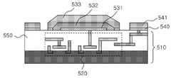
도 5를 참조하면 본 발명의 일 실시예에 따른 신호처리블록을 구비하는 적층형 마이크로폰에서 CMOS공정으로 신호처리블록(520)이 제작된 반도체 기판(510)의 표면은 제1금속층(531)과 외부 입출력패드(540) 및 보호막층(passivation layer, 550)으로 이루어진다Referring to FIG. 5, in a stacked microphone including a signal processing block according to an embodiment of the present invention, a surface of the
이때 상기 제1금속층(531)은 마이크로폰의 하부전극으로 사용되며 상기 제1금속층(531) 상부에 포토레지스터층(532)이 형성되어 있다. 이때 필요에 따라 상기 포토레지스터층(532)은 적당한 온도를 가하여 리플로우(reflow)과정을 거쳐 형성될 수 있다. 상기 포토레지스터층(532) 상부에는 제2금속층(533)이 형성되어 있다.In this case, the
상기 포토레지스터층(532) 상부에 형성된 제2금속층(533)과 입출력패드(540) 의 상부에 형성된 제2금속층(541)은 전기적 절연을 위해 분리되어 있다.The
상기 포토레지스터층(532)과 상기 제2금속층(533)은 마이크로폰의 진동판을 구성하고 이러한 진동판의 진동에 대한 특성은 포토레지스터층(532)의 특성에 의하여 주로 결정된다. 따라서 포토레지스터층(532)의 물리적 특성을 변화시키기 위하여 PR의 경화 과정 등을 거칠 수 있다.The
도 6 및 도 7은 본 발명의 다른 일 실시예에 따른 신호처리블록을 구비하는 적층형 마이크로폰의 단면도이다.6 and 7 are cross-sectional views of stacked microphones having a signal processing block according to another embodiment of the present invention.
도 6을 참조하면 본 발명의 다른 일 실시예에 따른 신호처리블록을 구비하는 적층형 마이크로폰에서 상기 제2금속층(533)에 복수의 음향홀(534)이 형성되어 있음을 알 수 있다.Referring to FIG. 6, it can be seen that a plurality of
또한 상기 포토레지스터층(532)은 상기 복수의 음향홀(534)을 통한 에칭에 의해 제거되어 상기 제1금속층(531)과 상기 제2금속층(533) 사이가 비어있는 구조를 이룬다.In addition, the
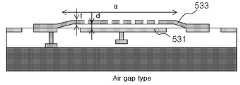
도 6에 도시된 본 발명의 다른 일 실시예에 따른 신호처리블록을 구비하는 적층형 마이크로폰에서는 상기 제2금속층(533)만이 진동판의 기능을 한다.In the stacked microphone including the signal processing block according to another embodiment of the present invention shown in FIG. 6, only the
상기 본 발명의 다른 일 실시예에 따른 신호처리블록을 구비하는 적층형 마이크로폰의 진동은 진동판을 형성하는 상기 제2금속층(533)의 물리적 특성(탄성계수, 내부응력 등)과 상기 제2금속층(533)의 두께(t), 진동판의 지름(a)등에 의하여 결정되며, 전기적 특성(정전용량)은 진동판의 면적 및 상기 제1금속층(531)과 상기 제2금속층(533) 사이의 거리(d)에 의하여 결정된다. 따라서 증착되는 상기 제2금속 층(533)의 두께는 위의 특성들을 고려하여 선택될 수 있다.Vibration of the stacked microphone having the signal processing block according to another embodiment of the present invention is the physical characteristics (elastic coefficient, internal stress, etc.) and the
도 8은 본 발명의 일 실시예에 따른 신호처리블록을 구비하는 적층형 마이크로폰의 진동판의 평면도이고, 도 9는 본 발명의 일 실시예에 따른 신호처리블록을 구비하는 적층형 마이크로폰의 진동판의 측면도이다.8 is a plan view of a diaphragm of a stacked microphone including a signal processing block according to an embodiment of the present invention, and FIG. 9 is a side view of a diaphragm of a stacked microphone including a signal processing block according to an embodiment of the present invention.
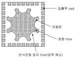
도 8을 참조하면, 진동판은 원형 또는 다각형의 형상을 갖고 복수의 음향홀을 가진다. 상기 진동판의 둘레에는 복수의 반사진동 방지홀이 형성되어 있다.Referring to FIG. 8, the diaphragm has a circular or polygonal shape and has a plurality of sound holes. A plurality of reflection vibration prevention holes are formed around the diaphragm.
음향홀은 제작과정에서 내부에 있게 되는 포토레지스터층을 제거하는데 사용되며, 진동판의 주파수특성을 균일하게 만드는 용도로 사용된다. 상기의 형태로 제작되는 진동판의 측면은 도 9에 도시된 바와 같다.Acoustic holes are used to remove the photoresist layer inside the fabrication process and to make the frequency characteristics of the diaphragm uniform. Sides of the diaphragm produced in the above form is as shown in FIG.
진동판은 진동판 고정 패드에 연결되며, 진동판 고정 패드는 다른 전극에 연결된다. 상기 진동판에 음향진동이 입사하는 경우 진동판은 진동하며, 진동판의 진동에 의해 발생한 반사 진동은 측면의 반사 진동 방지 홀을 통하여 외부로 유출된다. 따라서 내부구조에 의한 공진이 억제된다. 또한 진동판에 고주파의 잡음진동이 입사하는 경우 음향홀(hole)에 의하여 고주파 진동이 억제된다.The diaphragm is connected to the diaphragm fixing pad, and the diaphragm fixing pad is connected to the other electrode. When the acoustic vibration is incident on the diaphragm, the diaphragm vibrates, and the reflected vibration generated by the vibration of the diaphragm flows out through the anti-reflection vibration holes on the side surface. Therefore, resonance due to the internal structure is suppressed. In addition, when a high frequency noise vibration is incident on the diaphragm, the high frequency vibration is suppressed by a sound hole.
도 10은 본 발명의 또 다른 일 실시예에 따른 신호처리블록을 구비하는 적층형 마이크로폰의 단면도이다.10 is a cross-sectional view of a stacked microphone having a signal processing block according to another embodiment of the present invention.
도 10에 도시된 본 발명의 또 다른 일 실시예에 따른 신호처리블록을 구비하는 적층형 마이크로폰은 상기 제2금속층(533)의 상부에 금속도금층(535)을 더 구비하고 있다. 상기 제2금속층(533)에 형성된 복수의 음향홀(534)은 상기 금속도금층(535)에 연통되어 있으며, 상기 금속도금층은 주로 금(Au) 또는 크롬(Cr) 재질의 금속을 전기도금 하여 형성된다.The stacked microphone including the signal processing block according to another exemplary embodiment of the present invention illustrated in FIG. 10 further includes a
도 11은 도 5에 도시된 본 발명의 일 실시예에 따른 신호처리블록을 구비하는 적층형 마이크로폰의 제조 공정을 나타내는 도면이다.FIG. 11 is a view illustrating a manufacturing process of a stacked microphone having a signal processing block according to an embodiment of the present invention shown in FIG. 5.
도 11에 도시된 바와 같이 본 발명의 일 실시예에 따른 신호처리블록을 구비하는 적층형 마이크로폰의 제조 공정은, (a) 반도체 기판(510) 상에 CMOS 공정을 통해 신호처리블록(520)을 제조하고 상기 반도체 기판의 표면에 제1금속층(531)과 입출력패드(540)를 형성하는 단계; (b) 상기 제1금속층의 상부에 포토레지스터층(532)을 형성하는 단계; (c) 필요에 따라 상기 포토레지스터층을 리플로우(reflow)하는 단계; (d) 상기 포토레지스터층이 형성된 상기 반도체 기판의 상부에 제2금속층(533)을 형성하는 단계; (e) 전기적 절연을 위해 상기 포토레지스터층의 상부에 형성된 상기 제2금속층(533)과 상기 입출력 패드(540)의 상부에 형성된 상기 제2금속층(541)을 분리하는 단계;를 구비한다.As shown in FIG. 11, in the manufacturing process of the stacked microphone including the signal processing block according to the exemplary embodiment of the present invention, (a) the
이러한 방법에 의해 형성된 진동판은 제2금속층(533)과 포토레지스터층(532)으로 구성되므로 진동에 대한 특성은 포토레지스터층의 특성에 의해 주로 결정된다.Since the diaphragm formed by this method consists of the
도 12는 도 6에 도시된 본 발명의 다른 일 실시예에 따른 신호처리블록을 구비하는 적층형 마이크로폰의 제조 공정을 나타내는 도면이다.FIG. 12 is a view illustrating a manufacturing process of a stacked microphone having a signal processing block according to another embodiment of the present invention shown in FIG. 6.
도 12에 도시된 바와 같이 본 발명의 다른 일 실시예에 따른 신호처리블록을 구비하는 적층형 마이크로폰의 제조 공정은, (a) 반도체 기판(510) 상에 CMOS 공정을 통해 신호처리블록(520)을 제조하고 상기 반도체 기판의 표면에 제1금속층(531) 과 입출력패드(540)를 형성하는 단계; (b) 상기 제1금속층(531)의 상부에 포토레지스터층(532)을 형성하는 단계; (c) 필요에 따라 상기 포토레지스터층을 리플로우(reflow)하는 단계; (d) 상기 포토레지스터층이 형성된 상기 반도체 기판의 상부에 제2금속층(533)을 형성하는 단계; (e) 전기적 절연을 위해 상기 포토레지스터층의 상부에 형성된 상기 제2금속층(533)과 상기 입출력 패드(540)의 상부에 형성된 상기 제2금속층(541)을 분리하고 상기 포토레지스터층의 상부에 형성된 상기 제2금속층(533)에 복수의 음향홀(534)을 형성하는 단계; (f) 상기 복수의 음향홀(534)을 통해 상기 포토레지스터층(532)을 에칭하여 제거하는 단계;를 구비한다.As shown in FIG. 12, a manufacturing method of a stacked microphone including a signal processing block according to another exemplary embodiment of the present invention includes (a) performing a
도 12를 참고하면 제2금속층(533)을 형성하는 (d)단계까지는 도 11에 도시된 제조 공정과 동일하다. 이후 (e)전기적 절연을 위해 상기 포토레지스터층(532)의 상부에 형성된 상기 제2금속층(533)과 상기 입출력 패드(540)의 상부에 형성된 상기 제2금속층(541)을 분리하는 단계에서 진동판에 음향홀(534)을 형성하고 이후 에칭에 의해 포토레지스터층(532)을 제거함으로써 제1금속층(531)과 제2금속층(533) 사이가 비어있는 구조를 형성할 수 있다.Referring to FIG. 12, the process up to (d) of forming the
도 13은 도 10에 도시된 본 발명의 또 다른 일 실시예에 따른 신호처리블록을 구비하는 적층형 마이크로폰의 제조 공정을 나타내는 도면이다.FIG. 13 is a view illustrating a manufacturing process of a stacked microphone having a signal processing block according to another embodiment of the present invention shown in FIG. 10.
도 13에 도시된 바와 같이 본 발명의 또 다른 일 실시예에 따른 신호처리블록을 구비하는 적층형 마이크로폰의 제조 공정은, (a) 반도체 기판(510) 상에 CMOS 공정을 통해 신호처리블록(520)을 제조하고 상기 반도체 기판의 표면에 제1금속층(531)과 입출력패드(540)를 형성하는 단계; (b) 상기 제1금속층(531)의 상부에 포토레지스터층(532)을 형성하는 단계; (c) 필요에 따라 상기 포토레지스터층을 리플로우(reflow)하는 단계; (d) 상기 포토레지스터층이 형성된 상기 반도체 기판의 상부에 제2금속층(533)을 형성하는 단계; (e) 전기적 절연을 위해 상기 포토레지스터층의 상부에 형성된 상기 제2금속층(533)과 상기 입출력 패드(540)의 상부에 형성된 상기 제2금속층(541)을 분리하고 상기 포토레지스터층의 상부에 형성된 상기 제2금속층(533)에 복수의 음향홀(534)을 형성하고 상기 제2금속층이 형성된 상기 반도체 기판의 상부에 금속의 전기도금을 위한 접착층(561)을 형성하는 단계; (f) 도금방지 포토레지스터층을 형성하고 상기 도금방지용 포토레지스터층(563)이 형성되지 아니한 부분을 전기도금하여 금속도금층(562)을 형성하는 단계 및 (g)상기 도금방지용 포토레지스터층(563)을 에칭하여 제거하는 단계;를 구비한다.As shown in FIG. 13, a manufacturing method of a stacked microphone including a signal processing block according to another embodiment of the present invention includes (a) a
이러한 방법에 의한 진동판은 제2금속층(533)과 금속도금층(562)으로 구성되며 증착과 도금을 병행하여 제작할 수 있다.The diaphragm according to this method is composed of the
이상으로, 본 발명은 도면에 도시된 실시예를 참고로 설명되었으나 이는 예시적인 것에 불과하며, 본 기술 분야의 통상의 지식을 가진 자라면 이로부터 다양한 변형 및 균등한 타 실시예가 가능하다는 점을 이해할 것이다. 따라서, 본 발명의 진정한 기술적 보호 범위는 첨부된 등록청구범위의 기술적 사상에 의해 정해져야 할 것이다.As described above, the present invention has been described with reference to the embodiments illustrated in the drawings, which are merely exemplary, and it should be understood by those skilled in the art that various modifications and equivalent other embodiments are possible. will be. Therefore, the true technical protection scope of the present invention will be defined by the technical spirit of the appended claims.
도 1은 본 발명의 실시 예에 따른 신호처리블록을 구비하는 적층형 마이크로폰의 구성을 나타내는 도면이다.1 is a view showing the configuration of a stacked microphone having a signal processing block according to an embodiment of the present invention.
도 2는 본 발명의 일 실시예에 따른 신호처리블록을 구비하는 적층형 마이크로폰의 회로의 구성도이다.2 is a block diagram of a circuit of a stacked microphone having a signal processing block according to an embodiment of the present invention.
도 3은 본 발명의 다른 일 실시예에 따른 신호처리블록을 구비하는 적층형 마이크로폰의 회로의 구성도이다.3 is a block diagram of a circuit of a stacked microphone having a signal processing block according to another embodiment of the present invention.
도 4는 본 발명의 또 다른 일 실시예에 따른 신호처리블록을 구비하는 적층형 마이크로폰의 회로의 구성도이다.4 is a block diagram of a circuit of a stacked microphone having a signal processing block according to another embodiment of the present invention.
도 5는 본 발명의 일 실시예에 따른 신호처리블록을 구비하는 적층형 마이크로폰의 단면도이다.5 is a cross-sectional view of a stacked microphone having a signal processing block according to an embodiment of the present invention.
도 6은 본 발명의 다른 일 실시예에 따른 신호처리블록을 구비하는 적층형 마이크로폰의 단면도이다.6 is a cross-sectional view of a stacked microphone having a signal processing block according to another embodiment of the present invention.
도 7은 본 발명의 다른 일 실시예에 따른 신호처리블록을 구비하는 적층형 마이크로폰의 단면도이다.7 is a cross-sectional view of a stacked microphone having a signal processing block according to another embodiment of the present invention.
도 8은 본 발명의 일 실시예에 따른 신호처리블록을 구비하는 적층형 마이크로폰의 진동판의 평면도이다.8 is a plan view of a diaphragm of a stacked microphone having a signal processing block according to an embodiment of the present invention.
도 9는 본 발명의 일 실시예에 따른 신호처리블록을 구비하는 적층형 마이크로폰의 진동판의 측면도이다.9 is a side view of a diaphragm of a stacked microphone having a signal processing block according to an embodiment of the present invention.
도 10은 본 발명의 또 다른 일 실시예에 따른 신호처리블록을 구비하는 적층형 마이크로폰의 단면도이다.10 is a cross-sectional view of a stacked microphone having a signal processing block according to another embodiment of the present invention.
도 11은 도 5에 도시된 본 발명의 일 실시예에 따른 신호처리블록을 구비하는 적층형 마이크로폰의 제조 공정을 나타내는 도면이다.FIG. 11 is a view illustrating a manufacturing process of a stacked microphone having a signal processing block according to an embodiment of the present invention shown in FIG. 5.
도 12는 도 6에 도시된 본 발명의 다른 일 실시예에 따른 신호처리블록을 구비하는 적층형 마이크로폰의 제조 공정을 나타내는 도면이다.FIG. 12 is a view illustrating a manufacturing process of a stacked microphone having a signal processing block according to another embodiment of the present invention shown in FIG. 6.
도 13은 도 10에 도시된 본 발명의 또 다른 일 실시예에 따른 신호처리블록을 구비하는 적층형 마이크로폰의 제조 공정을 나타내는 도면이다.FIG. 13 is a view illustrating a manufacturing process of a stacked microphone having a signal processing block according to another embodiment of the present invention shown in FIG. 10.
Claims (16)
Translated fromKoreanPriority Applications (2)
| Application Number | Priority Date | Filing Date | Title |
|---|---|---|---|
| KR1020080018083AKR100878454B1 (en) | 2008-02-28 | 2008-02-28 | Stacked microphone with signal processing block and method for manufacturing same |
| PCT/KR2009/000695WO2009107940A2 (en) | 2008-02-28 | 2009-02-13 | Stacked microphone with signal processing block and method for manufacturing same |
Applications Claiming Priority (1)
| Application Number | Priority Date | Filing Date | Title |
|---|---|---|---|
| KR1020080018083AKR100878454B1 (en) | 2008-02-28 | 2008-02-28 | Stacked microphone with signal processing block and method for manufacturing same |
Publications (1)
| Publication Number | Publication Date |
|---|---|
| KR100878454B1true KR100878454B1 (en) | 2009-01-13 |
Family
ID=40482589
Family Applications (1)
| Application Number | Title | Priority Date | Filing Date |
|---|---|---|---|
| KR1020080018083AExpired - Fee RelatedKR100878454B1 (en) | 2008-02-28 | 2008-02-28 | Stacked microphone with signal processing block and method for manufacturing same |
Country Status (2)
| Country | Link |
|---|---|
| KR (1) | KR100878454B1 (en) |
| WO (1) | WO2009107940A2 (en) |
Families Citing this family (7)
| Publication number | Priority date | Publication date | Assignee | Title |
|---|---|---|---|---|
| US9533873B2 (en) | 2013-02-05 | 2017-01-03 | Butterfly Network, Inc. | CMOS ultrasonic transducers and related apparatus and methods |
| EP4122609B1 (en) | 2013-03-15 | 2024-11-06 | BFLY Operations, Inc. | Complementary metal oxide semiconductor (cmos) ultrasonic transducers and methods for forming the same |
| AU2015247484B2 (en) | 2014-04-18 | 2020-05-14 | Butterfly Network, Inc. | Ultrasonic transducers in complementary metal oxide semiconductor (CMOS) wafers and related apparatus and methods |
| US9067779B1 (en) | 2014-07-14 | 2015-06-30 | Butterfly Network, Inc. | Microfabricated ultrasonic transducers and related apparatus and methods |
| US9987661B2 (en) | 2015-12-02 | 2018-06-05 | Butterfly Network, Inc. | Biasing of capacitive micromachined ultrasonic transducers (CMUTs) and related apparatus and methods |
| US10196261B2 (en) | 2017-03-08 | 2019-02-05 | Butterfly Network, Inc. | Microfabricated ultrasonic transducers and related apparatus and methods |
| WO2018236956A1 (en) | 2017-06-21 | 2018-12-27 | Butterfly Network, Inc. | MICROFABRICATED ULTRASONIC TRANSDUCER HAVING INDIVIDUAL CELLS HAVING ELECTRICALLY ISOLATED ELECTRODE SECTIONS |
Citations (5)
| Publication number | Priority date | Publication date | Assignee | Title |
|---|---|---|---|---|
| KR100409273B1 (en)* | 2001-07-07 | 2003-12-11 | 주식회사 비에스이 | A chip microphone |
| KR20040046544A (en)* | 2002-11-27 | 2004-06-05 | 전자부품연구원 | Method for manufacturing acoustic transducer |
| JP2004223708A (en) | 2003-01-23 | 2004-08-12 | Akustica Inc | Multi-metal layer mems structure and process to manufacture it |
| KR100506820B1 (en) | 2002-12-31 | 2005-08-10 | 전자부품연구원 | Method for manufacturing acoustic transducer |
| KR20080006579A (en)* | 2006-01-11 | 2008-01-16 | 오스트리아마이크로시스템즈 아게 | MEMS sensor and manufacturing method |
Family Cites Families (3)
| Publication number | Priority date | Publication date | Assignee | Title |
|---|---|---|---|---|
| US5573679A (en)* | 1995-06-19 | 1996-11-12 | Alberta Microelectronic Centre | Fabrication of a surface micromachined capacitive microphone using a dry-etch process |
| KR100512960B1 (en)* | 2002-09-26 | 2005-09-07 | 삼성전자주식회사 | Flexible MEMS transducer and its manufacturing method, and flexible MEMS wireless microphone |
| KR100765149B1 (en)* | 2005-10-05 | 2007-10-15 | 전자부품연구원 | Ultra-small acoustic sensing device and manufacturing method thereof |
- 2008
- 2008-02-28KRKR1020080018083Apatent/KR100878454B1/ennot_activeExpired - Fee Related
- 2009
- 2009-02-13WOPCT/KR2009/000695patent/WO2009107940A2/enactiveApplication Filing
Patent Citations (5)
| Publication number | Priority date | Publication date | Assignee | Title |
|---|---|---|---|---|
| KR100409273B1 (en)* | 2001-07-07 | 2003-12-11 | 주식회사 비에스이 | A chip microphone |
| KR20040046544A (en)* | 2002-11-27 | 2004-06-05 | 전자부품연구원 | Method for manufacturing acoustic transducer |
| KR100506820B1 (en) | 2002-12-31 | 2005-08-10 | 전자부품연구원 | Method for manufacturing acoustic transducer |
| JP2004223708A (en) | 2003-01-23 | 2004-08-12 | Akustica Inc | Multi-metal layer mems structure and process to manufacture it |
| KR20080006579A (en)* | 2006-01-11 | 2008-01-16 | 오스트리아마이크로시스템즈 아게 | MEMS sensor and manufacturing method |
Also Published As
| Publication number | Publication date |
|---|---|
| WO2009107940A3 (en) | 2009-11-26 |
| WO2009107940A2 (en) | 2009-09-03 |
Similar Documents
| Publication | Publication Date | Title |
|---|---|---|
| US11197103B2 (en) | MEMS devices and processes | |
| KR100878454B1 (en) | Stacked microphone with signal processing block and method for manufacturing same | |
| KR100931575B1 (en) | Piezoelectric element micro speaker using MEMS and its manufacturing method | |
| EP1931173B1 (en) | Condenser microphone having flexure hinge diaphragm and method of manufacturing the same | |
| EP2663093B1 (en) | Sound transducer and microphone using same | |
| US8509462B2 (en) | Piezoelectric micro speaker including annular ring-shaped vibrating membranes and method of manufacturing the piezoelectric micro speaker | |
| US7856804B2 (en) | MEMS process and device | |
| US8526642B2 (en) | Piezoelectric micro speaker including weight attached to vibrating membrane and method of manufacturing the same | |
| KR101807064B1 (en) | Microphone system and manufacturign the same | |
| US8401220B2 (en) | Piezoelectric micro speaker with curved lead wires and method of manufacturing the same | |
| KR101758017B1 (en) | Piezo mems microphone and thereof manufacturing method | |
| US10313799B2 (en) | Microphone and method for manufacturing the same | |
| JP2019517750A (en) | MEMS microphone and method for preparing the same | |
| KR20080052222A (en) | Condenser microphone with flexible spring type diaphragm and its manufacturing method | |
| WO2007010421A2 (en) | Mems microphone and package | |
| JP5097603B2 (en) | Microphone unit | |
| KR101938584B1 (en) | Mems microphone | |
| US8687827B2 (en) | Micro-electro-mechanical system microphone chip with expanded back chamber | |
| JP2008211466A (en) | Microphone package, microphone mounted body, microphone device | |
| KR20090119268A (en) | Silicon condenser microphone and method of manufacturing silicon chip used therein | |
| KR102297885B1 (en) | MEMS microphone having sound inflow structure | |
| KR101460205B1 (en) | Mems microphone having sound-pass member | |
| US20250126386A1 (en) | MEMS microphone | |
| KR20230133807A (en) | Durability reinforced mems microphone and manufacturing method thereof | |
| JP2004147152A (en) | Acoustic sensor and method of manufacturing the same |
Legal Events
| Date | Code | Title | Description |
|---|---|---|---|
| A201 | Request for examination | ||
| PA0109 | Patent application | St.27 status event code:A-0-1-A10-A12-nap-PA0109 | |
| PA0201 | Request for examination | St.27 status event code:A-1-2-D10-D11-exm-PA0201 | |
| A302 | Request for accelerated examination | ||
| PA0302 | Request for accelerated examination | St.27 status event code:A-1-2-D10-D17-exm-PA0302 St.27 status event code:A-1-2-D10-D16-exm-PA0302 | |
| D13-X000 | Search requested | St.27 status event code:A-1-2-D10-D13-srh-X000 | |
| D14-X000 | Search report completed | St.27 status event code:A-1-2-D10-D14-srh-X000 | |
| E902 | Notification of reason for refusal | ||
| PE0902 | Notice of grounds for rejection | St.27 status event code:A-1-2-D10-D21-exm-PE0902 | |
| E601 | Decision to refuse application | ||
| PE0601 | Decision on rejection of patent | St.27 status event code:N-2-6-B10-B15-exm-PE0601 | |
| AMND | Amendment | ||
| E13-X000 | Pre-grant limitation requested | St.27 status event code:A-2-3-E10-E13-lim-X000 | |
| J201 | Request for trial against refusal decision | ||
| P11-X000 | Amendment of application requested | St.27 status event code:A-2-2-P10-P11-nap-X000 | |
| P13-X000 | Application amended | St.27 status event code:A-2-2-P10-P13-nap-X000 | |
| PJ0201 | Trial against decision of rejection | St.27 status event code:A-3-3-V10-V11-apl-PJ0201 | |
| PB0901 | Examination by re-examination before a trial | St.27 status event code:A-6-3-E10-E12-rex-PB0901 | |
| E902 | Notification of reason for refusal | ||
| PE0902 | Notice of grounds for rejection | St.27 status event code:A-1-2-D10-D21-exm-PE0902 | |
| P11-X000 | Amendment of application requested | St.27 status event code:A-2-2-P10-P11-nap-X000 | |
| P13-X000 | Application amended | St.27 status event code:A-2-2-P10-P13-nap-X000 | |
| B701 | Decision to grant | ||
| PB0701 | Decision of registration after re-examination before a trial | St.27 status event code:A-3-4-F10-F13-rex-PB0701 | |
| GRNT | Written decision to grant | ||
| PR0701 | Registration of establishment | St.27 status event code:A-2-4-F10-F11-exm-PR0701 | |
| PR1002 | Payment of registration fee | St.27 status event code:A-2-2-U10-U11-oth-PR1002 Fee payment year number:1 | |
| PG1601 | Publication of registration | St.27 status event code:A-4-4-Q10-Q13-nap-PG1601 | |
| R18-X000 | Changes to party contact information recorded | St.27 status event code:A-5-5-R10-R18-oth-X000 | |
| R18-X000 | Changes to party contact information recorded | St.27 status event code:A-5-5-R10-R18-oth-X000 | |
| PR1001 | Payment of annual fee | St.27 status event code:A-4-4-U10-U11-oth-PR1001 Fee payment year number:4 | |
| FPAY | Annual fee payment | Payment date:20130131 Year of fee payment:5 | |
| PR1001 | Payment of annual fee | St.27 status event code:A-4-4-U10-U11-oth-PR1001 Fee payment year number:5 | |
| PN2301 | Change of applicant | St.27 status event code:A-5-5-R10-R13-asn-PN2301 St.27 status event code:A-5-5-R10-R11-asn-PN2301 | |
| FPAY | Annual fee payment | Payment date:20140106 Year of fee payment:6 | |
| PR1001 | Payment of annual fee | St.27 status event code:A-4-4-U10-U11-oth-PR1001 Fee payment year number:6 | |
| PN2301 | Change of applicant | St.27 status event code:A-5-5-R10-R13-asn-PN2301 St.27 status event code:A-5-5-R10-R11-asn-PN2301 | |
| R18-X000 | Changes to party contact information recorded | St.27 status event code:A-5-5-R10-R18-oth-X000 | |
| FPAY | Annual fee payment | Payment date:20150106 Year of fee payment:7 | |
| PR1001 | Payment of annual fee | St.27 status event code:A-4-4-U10-U11-oth-PR1001 Fee payment year number:7 | |
| FPAY | Annual fee payment | Payment date:20151221 Year of fee payment:8 | |
| PR1001 | Payment of annual fee | St.27 status event code:A-4-4-U10-U11-oth-PR1001 Fee payment year number:8 | |
| LAPS | Lapse due to unpaid annual fee | ||
| PC1903 | Unpaid annual fee | St.27 status event code:A-4-4-U10-U13-oth-PC1903 Not in force date:20170108 Payment event data comment text:Termination Category : DEFAULT_OF_REGISTRATION_FEE | |
| PC1903 | Unpaid annual fee | St.27 status event code:N-4-6-H10-H13-oth-PC1903 Ip right cessation event data comment text:Termination Category : DEFAULT_OF_REGISTRATION_FEE Not in force date:20170108 |