KR100877551B1 - Semiconductor package having electromagnetic shielding function, manufacturing method and jig - Google Patents
Semiconductor package having electromagnetic shielding function, manufacturing method and jigDownload PDFInfo
- Publication number
- KR100877551B1 KR100877551B1KR1020080050975AKR20080050975AKR100877551B1KR 100877551 B1KR100877551 B1KR 100877551B1KR 1020080050975 AKR1020080050975 AKR 1020080050975AKR 20080050975 AKR20080050975 AKR 20080050975AKR 100877551 B1KR100877551 B1KR 100877551B1
- Authority
- KR
- South Korea
- Prior art keywords
- semiconductor package
- sputtering
- shielding film
- semiconductor
- electromagnetic shielding
- Prior art date
- Legal status (The legal status is an assumption and is not a legal conclusion. Google has not performed a legal analysis and makes no representation as to the accuracy of the status listed.)
- Expired - Fee Related
Links
Images


Classifications
- H—ELECTRICITY
- H01—ELECTRIC ELEMENTS
- H01L—SEMICONDUCTOR DEVICES NOT COVERED BY CLASS H10
- H01L23/00—Details of semiconductor or other solid state devices
- H01L23/02—Containers; Seals
- H01L23/06—Containers; Seals characterised by the material of the container or its electrical properties
- H—ELECTRICITY
- H01—ELECTRIC ELEMENTS
- H01L—SEMICONDUCTOR DEVICES NOT COVERED BY CLASS H10
- H01L23/00—Details of semiconductor or other solid state devices
- H01L23/552—Protection against radiation, e.g. light or electromagnetic waves
- H—ELECTRICITY
- H01—ELECTRIC ELEMENTS
- H01L—SEMICONDUCTOR DEVICES NOT COVERED BY CLASS H10
- H01L24/00—Arrangements for connecting or disconnecting semiconductor or solid-state bodies; Methods or apparatus related thereto
- H01L24/93—Batch processes
- H01L24/95—Batch processes at chip-level, i.e. with connecting carried out on a plurality of singulated devices, i.e. on diced chips
- H01L24/97—Batch processes at chip-level, i.e. with connecting carried out on a plurality of singulated devices, i.e. on diced chips the devices being connected to a common substrate, e.g. interposer, said common substrate being separable into individual assemblies after connecting
- H—ELECTRICITY
- H01—ELECTRIC ELEMENTS
- H01L—SEMICONDUCTOR DEVICES NOT COVERED BY CLASS H10
- H01L2224/00—Indexing scheme for arrangements for connecting or disconnecting semiconductor or solid-state bodies and methods related thereto as covered by H01L24/00
- H01L2224/01—Means for bonding being attached to, or being formed on, the surface to be connected, e.g. chip-to-package, die-attach, "first-level" interconnects; Manufacturing methods related thereto
- H01L2224/42—Wire connectors; Manufacturing methods related thereto
- H01L2224/44—Structure, shape, material or disposition of the wire connectors prior to the connecting process
- H01L2224/45—Structure, shape, material or disposition of the wire connectors prior to the connecting process of an individual wire connector
- H01L2224/45001—Core members of the connector
- H01L2224/45099—Material
- H01L2224/451—Material with a principal constituent of the material being a metal or a metalloid, e.g. boron (B), silicon (Si), germanium (Ge), arsenic (As), antimony (Sb), tellurium (Te) and polonium (Po), and alloys thereof
- H01L2224/45117—Material with a principal constituent of the material being a metal or a metalloid, e.g. boron (B), silicon (Si), germanium (Ge), arsenic (As), antimony (Sb), tellurium (Te) and polonium (Po), and alloys thereof the principal constituent melting at a temperature of greater than or equal to 400°C and less than 950°C
- H01L2224/45124—Aluminium (Al) as principal constituent
- H—ELECTRICITY
- H01—ELECTRIC ELEMENTS
- H01L—SEMICONDUCTOR DEVICES NOT COVERED BY CLASS H10
- H01L2224/00—Indexing scheme for arrangements for connecting or disconnecting semiconductor or solid-state bodies and methods related thereto as covered by H01L24/00
- H01L2224/01—Means for bonding being attached to, or being formed on, the surface to be connected, e.g. chip-to-package, die-attach, "first-level" interconnects; Manufacturing methods related thereto
- H01L2224/42—Wire connectors; Manufacturing methods related thereto
- H01L2224/44—Structure, shape, material or disposition of the wire connectors prior to the connecting process
- H01L2224/45—Structure, shape, material or disposition of the wire connectors prior to the connecting process of an individual wire connector
- H01L2224/45001—Core members of the connector
- H01L2224/45099—Material
- H01L2224/451—Material with a principal constituent of the material being a metal or a metalloid, e.g. boron (B), silicon (Si), germanium (Ge), arsenic (As), antimony (Sb), tellurium (Te) and polonium (Po), and alloys thereof
- H01L2224/45138—Material with a principal constituent of the material being a metal or a metalloid, e.g. boron (B), silicon (Si), germanium (Ge), arsenic (As), antimony (Sb), tellurium (Te) and polonium (Po), and alloys thereof the principal constituent melting at a temperature of greater than or equal to 950°C and less than 1550°C
- H01L2224/45144—Gold (Au) as principal constituent
- H—ELECTRICITY
- H01—ELECTRIC ELEMENTS
- H01L—SEMICONDUCTOR DEVICES NOT COVERED BY CLASS H10
- H01L2224/00—Indexing scheme for arrangements for connecting or disconnecting semiconductor or solid-state bodies and methods related thereto as covered by H01L24/00
- H01L2224/01—Means for bonding being attached to, or being formed on, the surface to be connected, e.g. chip-to-package, die-attach, "first-level" interconnects; Manufacturing methods related thereto
- H01L2224/42—Wire connectors; Manufacturing methods related thereto
- H01L2224/47—Structure, shape, material or disposition of the wire connectors after the connecting process
- H01L2224/48—Structure, shape, material or disposition of the wire connectors after the connecting process of an individual wire connector
- H01L2224/4805—Shape
- H01L2224/4809—Loop shape
- H01L2224/48091—Arched
- H—ELECTRICITY
- H01—ELECTRIC ELEMENTS
- H01L—SEMICONDUCTOR DEVICES NOT COVERED BY CLASS H10
- H01L2224/00—Indexing scheme for arrangements for connecting or disconnecting semiconductor or solid-state bodies and methods related thereto as covered by H01L24/00
- H01L2224/01—Means for bonding being attached to, or being formed on, the surface to be connected, e.g. chip-to-package, die-attach, "first-level" interconnects; Manufacturing methods related thereto
- H01L2224/42—Wire connectors; Manufacturing methods related thereto
- H01L2224/47—Structure, shape, material or disposition of the wire connectors after the connecting process
- H01L2224/48—Structure, shape, material or disposition of the wire connectors after the connecting process of an individual wire connector
- H01L2224/481—Disposition
- H01L2224/48151—Connecting between a semiconductor or solid-state body and an item not being a semiconductor or solid-state body, e.g. chip-to-substrate, chip-to-passive
- H01L2224/48221—Connecting between a semiconductor or solid-state body and an item not being a semiconductor or solid-state body, e.g. chip-to-substrate, chip-to-passive the body and the item being stacked
- H01L2224/48225—Connecting between a semiconductor or solid-state body and an item not being a semiconductor or solid-state body, e.g. chip-to-substrate, chip-to-passive the body and the item being stacked the item being non-metallic, e.g. insulating substrate with or without metallisation
- H01L2224/48227—Connecting between a semiconductor or solid-state body and an item not being a semiconductor or solid-state body, e.g. chip-to-substrate, chip-to-passive the body and the item being stacked the item being non-metallic, e.g. insulating substrate with or without metallisation connecting the wire to a bond pad of the item
- H—ELECTRICITY
- H01—ELECTRIC ELEMENTS
- H01L—SEMICONDUCTOR DEVICES NOT COVERED BY CLASS H10
- H01L2224/00—Indexing scheme for arrangements for connecting or disconnecting semiconductor or solid-state bodies and methods related thereto as covered by H01L24/00
- H01L2224/93—Batch processes
- H01L2224/95—Batch processes at chip-level, i.e. with connecting carried out on a plurality of singulated devices, i.e. on diced chips
- H01L2224/97—Batch processes at chip-level, i.e. with connecting carried out on a plurality of singulated devices, i.e. on diced chips the devices being connected to a common substrate, e.g. interposer, said common substrate being separable into individual assemblies after connecting
- H—ELECTRICITY
- H01—ELECTRIC ELEMENTS
- H01L—SEMICONDUCTOR DEVICES NOT COVERED BY CLASS H10
- H01L24/00—Arrangements for connecting or disconnecting semiconductor or solid-state bodies; Methods or apparatus related thereto
- H01L24/01—Means for bonding being attached to, or being formed on, the surface to be connected, e.g. chip-to-package, die-attach, "first-level" interconnects; Manufacturing methods related thereto
- H01L24/42—Wire connectors; Manufacturing methods related thereto
- H01L24/44—Structure, shape, material or disposition of the wire connectors prior to the connecting process
- H01L24/45—Structure, shape, material or disposition of the wire connectors prior to the connecting process of an individual wire connector
- H—ELECTRICITY
- H01—ELECTRIC ELEMENTS
- H01L—SEMICONDUCTOR DEVICES NOT COVERED BY CLASS H10
- H01L24/00—Arrangements for connecting or disconnecting semiconductor or solid-state bodies; Methods or apparatus related thereto
- H01L24/01—Means for bonding being attached to, or being formed on, the surface to be connected, e.g. chip-to-package, die-attach, "first-level" interconnects; Manufacturing methods related thereto
- H01L24/42—Wire connectors; Manufacturing methods related thereto
- H01L24/47—Structure, shape, material or disposition of the wire connectors after the connecting process
- H01L24/48—Structure, shape, material or disposition of the wire connectors after the connecting process of an individual wire connector
- H—ELECTRICITY
- H01—ELECTRIC ELEMENTS
- H01L—SEMICONDUCTOR DEVICES NOT COVERED BY CLASS H10
- H01L2924/00—Indexing scheme for arrangements or methods for connecting or disconnecting semiconductor or solid-state bodies as covered by H01L24/00
- H01L2924/01—Chemical elements
- H01L2924/01004—Beryllium [Be]
- H—ELECTRICITY
- H01—ELECTRIC ELEMENTS
- H01L—SEMICONDUCTOR DEVICES NOT COVERED BY CLASS H10
- H01L2924/00—Indexing scheme for arrangements or methods for connecting or disconnecting semiconductor or solid-state bodies as covered by H01L24/00
- H01L2924/01—Chemical elements
- H01L2924/01006—Carbon [C]
- H—ELECTRICITY
- H01—ELECTRIC ELEMENTS
- H01L—SEMICONDUCTOR DEVICES NOT COVERED BY CLASS H10
- H01L2924/00—Indexing scheme for arrangements or methods for connecting or disconnecting semiconductor or solid-state bodies as covered by H01L24/00
- H01L2924/01—Chemical elements
- H01L2924/01013—Aluminum [Al]
- H—ELECTRICITY
- H01—ELECTRIC ELEMENTS
- H01L—SEMICONDUCTOR DEVICES NOT COVERED BY CLASS H10
- H01L2924/00—Indexing scheme for arrangements or methods for connecting or disconnecting semiconductor or solid-state bodies as covered by H01L24/00
- H01L2924/01—Chemical elements
- H01L2924/01018—Argon [Ar]
- H—ELECTRICITY
- H01—ELECTRIC ELEMENTS
- H01L—SEMICONDUCTOR DEVICES NOT COVERED BY CLASS H10
- H01L2924/00—Indexing scheme for arrangements or methods for connecting or disconnecting semiconductor or solid-state bodies as covered by H01L24/00
- H01L2924/01—Chemical elements
- H01L2924/01027—Cobalt [Co]
- H—ELECTRICITY
- H01—ELECTRIC ELEMENTS
- H01L—SEMICONDUCTOR DEVICES NOT COVERED BY CLASS H10
- H01L2924/00—Indexing scheme for arrangements or methods for connecting or disconnecting semiconductor or solid-state bodies as covered by H01L24/00
- H01L2924/01—Chemical elements
- H01L2924/01028—Nickel [Ni]
- H—ELECTRICITY
- H01—ELECTRIC ELEMENTS
- H01L—SEMICONDUCTOR DEVICES NOT COVERED BY CLASS H10
- H01L2924/00—Indexing scheme for arrangements or methods for connecting or disconnecting semiconductor or solid-state bodies as covered by H01L24/00
- H01L2924/01—Chemical elements
- H01L2924/01029—Copper [Cu]
- H—ELECTRICITY
- H01—ELECTRIC ELEMENTS
- H01L—SEMICONDUCTOR DEVICES NOT COVERED BY CLASS H10
- H01L2924/00—Indexing scheme for arrangements or methods for connecting or disconnecting semiconductor or solid-state bodies as covered by H01L24/00
- H01L2924/01—Chemical elements
- H01L2924/01033—Arsenic [As]
- H—ELECTRICITY
- H01—ELECTRIC ELEMENTS
- H01L—SEMICONDUCTOR DEVICES NOT COVERED BY CLASS H10
- H01L2924/00—Indexing scheme for arrangements or methods for connecting or disconnecting semiconductor or solid-state bodies as covered by H01L24/00
- H01L2924/01—Chemical elements
- H01L2924/01047—Silver [Ag]
- H—ELECTRICITY
- H01—ELECTRIC ELEMENTS
- H01L—SEMICONDUCTOR DEVICES NOT COVERED BY CLASS H10
- H01L2924/00—Indexing scheme for arrangements or methods for connecting or disconnecting semiconductor or solid-state bodies as covered by H01L24/00
- H01L2924/01—Chemical elements
- H01L2924/0105—Tin [Sn]
- H—ELECTRICITY
- H01—ELECTRIC ELEMENTS
- H01L—SEMICONDUCTOR DEVICES NOT COVERED BY CLASS H10
- H01L2924/00—Indexing scheme for arrangements or methods for connecting or disconnecting semiconductor or solid-state bodies as covered by H01L24/00
- H01L2924/01—Chemical elements
- H01L2924/01078—Platinum [Pt]
- H—ELECTRICITY
- H01—ELECTRIC ELEMENTS
- H01L—SEMICONDUCTOR DEVICES NOT COVERED BY CLASS H10
- H01L2924/00—Indexing scheme for arrangements or methods for connecting or disconnecting semiconductor or solid-state bodies as covered by H01L24/00
- H01L2924/01—Chemical elements
- H01L2924/01079—Gold [Au]
- H—ELECTRICITY
- H01—ELECTRIC ELEMENTS
- H01L—SEMICONDUCTOR DEVICES NOT COVERED BY CLASS H10
- H01L2924/00—Indexing scheme for arrangements or methods for connecting or disconnecting semiconductor or solid-state bodies as covered by H01L24/00
- H01L2924/01—Chemical elements
- H01L2924/01082—Lead [Pb]
- H—ELECTRICITY
- H01—ELECTRIC ELEMENTS
- H01L—SEMICONDUCTOR DEVICES NOT COVERED BY CLASS H10
- H01L2924/00—Indexing scheme for arrangements or methods for connecting or disconnecting semiconductor or solid-state bodies as covered by H01L24/00
- H01L2924/10—Details of semiconductor or other solid state devices to be connected
- H01L2924/11—Device type
- H01L2924/12—Passive devices, e.g. 2 terminal devices
- H01L2924/1204—Optical Diode
- H01L2924/12042—LASER
- H—ELECTRICITY
- H01—ELECTRIC ELEMENTS
- H01L—SEMICONDUCTOR DEVICES NOT COVERED BY CLASS H10
- H01L2924/00—Indexing scheme for arrangements or methods for connecting or disconnecting semiconductor or solid-state bodies as covered by H01L24/00
- H01L2924/10—Details of semiconductor or other solid state devices to be connected
- H01L2924/146—Mixed devices
- H01L2924/1461—MEMS
- H—ELECTRICITY
- H01—ELECTRIC ELEMENTS
- H01L—SEMICONDUCTOR DEVICES NOT COVERED BY CLASS H10
- H01L2924/00—Indexing scheme for arrangements or methods for connecting or disconnecting semiconductor or solid-state bodies as covered by H01L24/00
- H01L2924/15—Details of package parts other than the semiconductor or other solid state devices to be connected
- H01L2924/161—Cap
- H01L2924/1615—Shape
- H01L2924/16152—Cap comprising a cavity for hosting the device, e.g. U-shaped cap
- H—ELECTRICITY
- H01—ELECTRIC ELEMENTS
- H01L—SEMICONDUCTOR DEVICES NOT COVERED BY CLASS H10
- H01L2924/00—Indexing scheme for arrangements or methods for connecting or disconnecting semiconductor or solid-state bodies as covered by H01L24/00
- H01L2924/30—Technical effects
- H01L2924/301—Electrical effects
- H01L2924/30105—Capacitance
- H—ELECTRICITY
- H01—ELECTRIC ELEMENTS
- H01L—SEMICONDUCTOR DEVICES NOT COVERED BY CLASS H10
- H01L2924/00—Indexing scheme for arrangements or methods for connecting or disconnecting semiconductor or solid-state bodies as covered by H01L24/00
- H01L2924/30—Technical effects
- H01L2924/301—Electrical effects
- H01L2924/3025—Electromagnetic shielding
Landscapes
- Power Engineering (AREA)
- Engineering & Computer Science (AREA)
- Computer Hardware Design (AREA)
- Microelectronics & Electronic Packaging (AREA)
- Physics & Mathematics (AREA)
- Condensed Matter Physics & Semiconductors (AREA)
- General Physics & Mathematics (AREA)
- Health & Medical Sciences (AREA)
- Electromagnetism (AREA)
- Toxicology (AREA)
- Shielding Devices Or Components To Electric Or Magnetic Fields (AREA)
- Structures Or Materials For Encapsulating Or Coating Semiconductor Devices Or Solid State Devices (AREA)
- Physical Vapour Deposition (AREA)
Abstract
Translated fromKoreanDescription
Translated fromKorean본 발명은 전자파 차폐 기능을 갖는 반도체 패키지 및 그 제조방법에 관한 것으로서, 보다 상세하게는, 반도체 패키지의 표면에 스퍼터링 방법으로 니켈합금을 코팅함으로써, 전자파를 차폐할 수 있도록 하는 전자파 차폐 기능을 갖는 반도체 패키지 및 그 제조방법에 관한 것이다.BACKGROUND OF THE
반도체가 개발된 이후, 반도체는 가전기기, 산업기기, 의료기기 등 다양한 전자제품에 채용되어 기기의 소형화, 경량화, 다기능화되고 있으며, 기기의 디지털화 또한 급속히 추진되고 있다.Since the development of semiconductors, semiconductors have been adopted for various electronic products such as home appliances, industrial devices, and medical devices, and have been miniaturized, lightweight, and multifunctional, and digitalization of devices is also rapidly being promoted.
일반적으로 반도체 소자는 마이크로 프로세서의 속도에 따라 50MHz 내지 3GHz의 전자기파를 방출하며, 최근 고속 마이크로프로세서의 개발과 고속 네트워킹 및 스위칭 용량이 급속히 증가함에 따라, 전자기파의 방출량이 증가하고 있다. 즉, 기기의 디지털화에 따라 점점 더 많은 양의 전자기파가 방출되고 있으며, 이러한 전자기파는 타 기기의 동작을 방해하는 EMI(Electromagnetic Interference)나 RFI(Radio Frequency Interference)로 작용하게 된다. 예를 들어, EMI 나 RFI에 의해, 자동설비 시스템이나 항공기 등의 첨단장비가 오작동하거나 작동이 정지되는 등의 문제가 발생하고 있다. 이러한 오작동이나 작동 정지는 막대한 재산피해를 발생시킬 수 있으며, 심지어는 인명피해도 발생시킬 수 있다.In general, semiconductor devices emit electromagnetic waves of 50 MHz to 3 GHz depending on the speed of the microprocessor. Recently, with the development of high speed microprocessors and the rapid growth of high speed networking and switching capacity, the amount of electromagnetic waves is increasing. That is, with the digitization of devices, more and more electromagnetic waves are emitted, and these electromagnetic waves act as electromagnetic interference (EMI) or radio frequency interference (RFI) that interferes with the operation of other devices. For example, due to EMI or RFI, problems such as malfunctioning or stopping of high-tech equipment such as automatic equipment systems or aircrafts are occurring. Such malfunctions or stoppages can cause enormous property damage, even to life.
이에 따라, 반도체 소자의 EMI나 RFI를 차폐하기 위한 제안들이 있어왔다. 예를 들어, 미국 특허공개 US 7,109,410 에는 반도체 소자의 전자기파를 차폐하기 위해 금속 커버를 제작하여 반도체 소자에 장착시키고 있다. 그런데, 이렇게 금속 커버를 별도로 제작할 경우, 부품 수 증가에 따라 원가가 상승하고, 금속 커버를 장착시키기 위한 공정이 증가되므로 부품이 조립작업이 번거로워진다는 단점이 있다.Accordingly, there have been proposals for shielding EMI or RFI of semiconductor devices. For example, US Patent Publication US 7,109,410 manufactures and mounts a metal cover to a semiconductor device to shield electromagnetic waves of the semiconductor device. However, when the metal cover is manufactured separately, the cost increases as the number of parts increases, and the process for mounting the metal cover is increased, which makes it difficult to assemble the parts.
한편, 반도체 소자의 표면에 무전해 도금이나 스프레이 방식을 이용하여 도금하는 방법도 제안되어 있으나, 무전해 도금의 경우, 반도체 소자를 에칭 용액 또는 화학적 침전조에 침지시켜야 하므로 침지가 불가능한 패키지의 경우에는 도금 자체가 불가능하며, 스프레이 방식의 경우 도포 효율이 떨어지고 두께가 두껍고 불균일하여 박막을 형성하는데는 적합하지 않다.On the other hand, a method of plating the surface of the semiconductor device using an electroless plating or spray method is also proposed, but in the case of the electroless plating, the semiconductor device must be immersed in an etching solution or a chemical precipitation tank, and thus plating is impossible in a package that cannot be immersed. It is not possible by itself, and the spray method is not suitable for forming a thin film because of poor coating efficiency, thick and uneven thickness.
이에 따라, 반도체 소자의 표면에 박막의 전자파 차폐막을 간편한 방법으로 코팅할 수 있으며, 모든 종류의 반도체 소자에 적용가능한 전자파 차폐막 형성방법을 모색하여야 할 것이다.Accordingly, the electromagnetic wave shielding film of the thin film may be coated on the surface of the semiconductor device by a simple method, and a method of forming an electromagnetic shielding film applicable to all kinds of semiconductor devices should be sought.
본 발명의 목적은, 간편한 방법으로 반도체 패키지의 전자파를 차폐할 수 있도록 함으로써, 원가를 절감하고 모든 반도체 패키지에 적용가능한 전자파 차폐 기능을 갖는 반도체 패키지 및 그 제조방법을 제공하는 것이다.SUMMARY OF THE INVENTION An object of the present invention is to provide a semiconductor package having a function of shielding electromagnetic waves and applicable to all semiconductor packages, and a method of manufacturing the same, by reducing the electromagnetic wave of the semiconductor package by a simple method.
상기한 바와 같은 목적을 달성하기 위한 본 발명에 의한 전자파 차폐 기능을 갖는 반도체 패키지 제조방법은, 반도체 칩을 제조하는 반도체 제조 단계; 상기 칩을 서브스트레이트에 접합시키는 본딩 단계; 상기 칩의 표면에 몰드를 씌워 반도체 패키지를 제작하는 몰딩 단계; 및, 플라즈마 스퍼터링 장치를 이용하여 니켈이 포함된 금속을 상기 반도체 패키지의 표면에 코팅하여 전자파 차폐막을 형성하는 스퍼터링 단계;를 포함하는 것을 특징으로 한다.A semiconductor package manufacturing method having an electromagnetic shielding function according to the present invention for achieving the above object, the semiconductor manufacturing step of manufacturing a semiconductor chip; Bonding the chip to a substrate; Forming a semiconductor package by covering a surface of the chip with a mold; And a sputtering step of forming an electromagnetic shielding film by coating a metal containing nickel on the surface of the semiconductor package by using a plasma sputtering device.
상기 스퍼터링 단계에서 사용하는 타겟은 니켈과 은의 합금 또는 니켈과 구리의 합금인 것이 바람직하다.The target used in the sputtering step is preferably an alloy of nickel and silver or an alloy of nickel and copper.
상기 스퍼터링 단계는 진공도가 2.0 내지 3.0*10-3 Torr인 스퍼터링 챔버에 100 내지 150 sccm의 반응가스를 주입하여 20 내지 30분 동안 스퍼터링을 수행할 수 있다.The sputtering step may be performed by sputtering for 20 to 30 minutes by injecting a reaction gas of 100 to 150 sccm into the sputtering chamber having a vacuum degree of 2.0 to 3.0 * 10-3 Torr.
상기 스퍼터링 단계에서 코팅된 전자파 차폐막의 두께는, 4000 내지 8000 Å일 수 있다.The thickness of the electromagnetic shielding film coated in the sputtering step may be 4000 to 8000 kPa.
상기 각 반도체 패키지 사이가 일정 폭만큼 함몰되도록 일부 절단하는 제1싱귤레이션 단계; 상기 각 반도체 패키지를 상호 분리할 수 있도록 풀 컷으로 절단하는 제2싱귤레이션 단계;를 더 포함하며, 상기 스퍼터링 단계는, 상기 제1싱귤레이션 공정이 실행된 이후, 상기 제2싱귤레이션 공정의 전 또는 후에 시행될 수 있다.A first singulation step of partially cutting the semiconductor packages to be recessed by a predetermined width; And a second singulation step of cutting each semiconductor package into a full cut so that the semiconductor packages can be separated from each other. The sputtering step includes: after the first singulation process is performed, before the second singulation process. Or later.
상기 스퍼터링 단계의 전에, 상기 반도체 패키지의 표면 중 전자파 차폐막의 코팅을 필요로 하지 아니하는 영역을 차단하는 마스킹 단계를 더 포함하며; 상기 마스킹 단계에서는 마스크, 또는 상기 반도체 패키지를 상기 플라즈마 스퍼터링 장치에 수용하기 위한 지그를 사용하여 상기 영역을 차단할 수 있다.A masking step of blocking a region of the surface of the semiconductor package that does not require coating of the electromagnetic wave shielding film before the sputtering step; In the masking step, the region may be blocked by using a mask or a jig for accommodating the semiconductor package in the plasma sputtering apparatus.
한편, 상기 목적은, 인쇄회로기판; 상기 인쇄회로기판위에 안착된 반도체 칩; 및, 상기 칩을 감싸며, 표면의 적어도 일부분에 플라즈마 스퍼터링 장치에 의해 니켈이 포함된 금속으로 전자파 차폐막이 코팅된 몰드;를 포함하는 것을 특징으로 하는 전자파가 차폐되는 반도체 패키지에 의해서도 달성될 수 있다.On the other hand, the object is a printed circuit board; A semiconductor chip seated on the printed circuit board; And a mold surrounding the chip and having an electromagnetic shielding film coated with a metal containing nickel on at least a portion of a surface thereof by a plasma sputtering device. The semiconductor package may be shielded by electromagnetic waves.
상기 전자파 차폐막은 외부로 노출된 접지단자까지 연장되어 형성될 수 있다.The electromagnetic shielding film may extend to the ground terminal exposed to the outside.
반도체 패키지의 스퍼터링 코팅시, 상기 반도체 패키지의 일부가 노출되도록 수용하는 지그공과, 상기 지그공의 일측에 상기 반도체 패키지의 접지단자에 이르는 영역이 노출되도록 함몰된 접지홈이 형성될 수 있다.In the sputtering coating of the semiconductor package, a jig hole for accommodating a portion of the semiconductor package is exposed, and a ground groove recessed to expose an area reaching the ground terminal of the semiconductor package is exposed at one side of the jig hole.
본 발명에 의한 전자파 차폐 기능을 갖는 반도체 패키지 및 그 제조방법에 따르면, 반도체 패키지의 몰드 표면에 스퍼터링 방법을 이용하여 니켈과 은 또는 구리 합금으로 형성된 전자파 차폐막을 코팅함으로써, 전자파를 차폐할 수 있다. 따라서, 반도체 패키지에서 방출된 전자파에 의해 타 기기나 소자의 작동에 영향을 주어 오류가 발생하는 것을 방지할 수 있다. 또한, LGA와 같은 SIP 모듈 패키지, Punch QFN 패키지, 또는 Sawn QFN 패키지와 같은 반도체 패키지의 경우에도 전자파 차폐막의 코팅이 가능하므로, 전자파 차폐막을 다양한 반도체 패키지에 형성할 수 있다.According to the semiconductor package having the electromagnetic wave shielding function and the manufacturing method thereof according to the present invention, the electromagnetic wave can be shielded by coating the electromagnetic wave shielding film formed of nickel and silver or copper alloy using the sputtering method on the mold surface of the semiconductor package. Therefore, it is possible to prevent the occurrence of an error by affecting the operation of other devices or devices by the electromagnetic waves emitted from the semiconductor package. In addition, in the case of a SIP module package such as LGA, a Punch QFN package, or a semiconductor package such as a Sawn QFN package, the electromagnetic shielding film may be coated, and thus the electromagnetic shielding film may be formed in various semiconductor packages.
이와 같은 본 발명을 첨부도면에 의거하여 더욱 상세히 설명하면 다음과 같다.The present invention will be described in more detail based on the accompanying drawings as follows.
하기에서 본 발명을 설명함에 있어 관련된 공지 기능 또는 구성에 대한 구체적인 설명이 본 발명의 요지를 불필요하게 흐릴 수 있다고 판단되는 경우에는 그 상세한 설명을 생략할 것이다. 그리고 후술하는 용어들은 본 발명에서의 기능을 고려하여 정의된 용어들로서, 이는 사용자, 운용자의 의도 또는 관례 등에 따라 달라질 수 있으며, 이에 따라 각 용어의 의미는 본 명세서 전반에 걸친 내용을 토대로 해석되어야 할 것이다.In the following description of the present invention, detailed descriptions of well-known functions or configurations will be omitted if it is determined that the detailed description of the present invention may unnecessarily obscure the subject matter of the present invention. And the following terms are terms defined in consideration of functions in the present invention, which may vary according to the intention or custom of the user, operator, etc. Accordingly, the meaning of each term should be interpreted based on the contents throughout the present specification. will be.
도 1은 본 발명에 따른 전자파 차폐 기능을 갖는 반도체 모듈 패키지의 측단면도, 도 2는 도 1의 반도체 모듈 패키지의 제조공정도이다.1 is a side cross-sectional view of a semiconductor module package having an electromagnetic shielding function according to the present invention, Figure 2 is a manufacturing process diagram of the semiconductor module package of FIG.
본 SIP(System In Package) 모듈 패키지(10)는, 인쇄회로기판(15), 칩(14), 몰드(13)를 포함하며, 몰드(13)의 표면에 전자파를 차폐하기 위한 전자파 차폐막(11)이 코팅되어 있다. 이러한 SIP 모듈 패키지(10)의 하나로 반도체 패키지의 밑바닥에 칩 전극을 어레이 형태로 형성한 LGA(land grid array) 패키지(30)가 있다.The SIP (System In Package)
본 SIP 모듈 패키지(10)를 제조하는 공정은, 도 2에 도시된 바와 같이, 웨이퍼 쏘우(Saw)(S200), 부품표면실장(SMT:surface mount technology)(S210), 다이 본딩(Die Bonding)(S220), 와이어 본딩(S230), 몰딩(S240), 레이저 마킹(S250), 제1싱귤레이션(S260), 스퍼터링(S270), 제2싱귤레이션(S280)으로 이루어진다.The process of manufacturing the
웨이퍼 쏘우(S200)은, 웨이퍼상의 수많은 칩들을 분리하기 위해 다이아몬드 톱을 사용하여 웨이퍼를 절단하는 공정이며, 부품표면실장 공정(S210)은 인쇄회로기판(15)의 표면에 직접 실장할 수 있는 표면실장부품(SMC: surface mounted components)을 전자 회로에 부착시키는 공정이고, 다이 본딩(S220)은 칩(14)을 서브스트레이트(Substrate)에 접착시키는 공정이다. 와이어 본딩 공정(S230)은 칩(14) 상의 본딩 패드(Bonding Pad)와 리드 프레임을 금 또는 알루미늄 와이어(16)로 접합시켜주는 공정이다. 몰딩(S240)은 화학수지로 칩(14)과 금 또는 알루미늄 와이어를 밀봉해주는 공정이다.The wafer saw S200 is a process of cutting a wafer using a diamond saw to separate a large number of chips on the wafer, and the component surface mounting process S210 is a surface that can be directly mounted on the surface of the printed
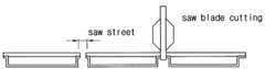
레이저 마킹 공정(S250)을 통해 필요한 글자들을 몰딩의 표면에 표시하고, 제1싱귤레이션 공정(S260)을 통해 각 반도체 모듈 패키지(10)를 하프 컷(Half cut)한다. 제1싱귤레이션 공정(S260)은, 하나의 스트립에 다수의 반도체 모듈 패키지(10)가 제조되기 때문에, 각 반도체 모듈 패키지(10)의 측면에 전자파 차폐막(11)을 코팅하기 위해서 반도체 모듈 패키지(10)의 측면을 노출하기 위해 수행된다.Necessary characters are displayed on the surface of the molding through a laser marking process (S250), and each
제1싱귤레이션 공정(S260)을 통해 도 3a에 도시된 바와 같이, 각 반도체 모듈 패키지(10) 사이가 함몰되어 각 반도체 모듈 패키지(10)의 측면이 형성된다. 그런 다음, 전자파 차폐막(11)이 형성되는 스퍼터링 공정(S270)이 수행되어 각 반도체 모듈 패키지(10)의 표면에, 도 3b에 도시된 바와 같이, 전자파 차폐막(11)이 코팅된다. 전자파 차폐막(11)이 코팅된 각 반도체 모듈 패키지(10)는, 제2싱귤레이션 공정(S280)을 통해 풀 컷(Full cut)되어 상호 분리된다. 한편, 스퍼터링 공정(S270)은 제2싱귤레이션 공정(S280)에 의해 모듈 패키지(10)가 풀 컷된 다음 수행될 수도 있다.As shown in FIG. 3A through the first singulation process S260, side surfaces of each
스퍼터링 공정(S270)에서 플라즈마 스퍼터링 장치를 이용하여 반도체 모듈 패키지(10)의 표면에 전자파 차폐막(11)을 코팅하는 공정을 일 실시예를 들어 상세히 살펴보면 다음과 같다.The process of coating the
제1싱귤레이션 공정(S260)을 통해 하프 컷된 반도체 모듈 패키지(10)와 타겟금속을 스퍼터링 챔버에 장착시키고, 코팅이 불필요한 PCB 뒷면을 차단한 후, 플라즈마 가스를 스퍼터링 챔버에 일정 압력으로 채운 다음, 전원을 공급하여 반도체 모듈 패키지(10)의 노출된 표면에 금속이 증착되도록 한다.After mounting the half-cut
본 실시예에 따른 스퍼터링 공정(S270)은 마그네트론 스퍼터링 시스템을 이용하여 수행되었으며, 스퍼터링 챔버의 진공도는 2.0 내지 3.0*10-3 Torr, 바람직하게는 2.5*10-3 Torr 이고, 반응가스로는 99.99%의 아르곤(Ar)을 100 내지 150 sccm 사용하였다. 이때, 반응가스의 양은 125sccm 이 바람직하다. 타겟금속으로는 니 켈과 은의 합금으로서, 니켈 90%, 은 10%를 사용하였으며, 니켈과 구리의 합금을 사용할 수 있음은 물론이다. 스퍼터링 코팅시간은 20분, 25분, 30분으로 가변하여, EMI의 발생량을 측정하였다.The sputtering process (S270) according to the present embodiment was performed using a magnetron sputtering system, the vacuum degree of the sputtering chamber is 2.0 to 3.0 * 10-3 Torr, preferably 2.5 * 10-3 Torr, 99.99% as a reaction gas Argon (Ar) of 100 to 150 sccm was used. At this time, the amount of the reaction gas is preferably 125sccm. As the target metal, nickel and silver were used as the alloy of nickel and 90% of nickel and 10% of silver. Of course, an alloy of nickel and copper may be used. Sputtering coating time was varied by 20 minutes, 25 minutes, 30 minutes, the amount of EMI was measured.
도 4에는 각각 스퍼터링 코팅시간을 20분, 25분, 30분으로 한 경우 EMI 테스트 결과를 보인 그래프이다.Figure 4 is a graph showing the EMI test results when the sputtering coating time to 20 minutes, 25 minutes, 30 minutes respectively.
그래프에서 Cell #1은 20분 동안 스퍼터링한 경우, Cell #2는 25분동안 스퍼터링한 경우, Cell #3는 30분 동안 스퍼터링한 경우, No-shield는 전자파 차폐막(11)을 형성하지 아니한 경우를 나타내며, 20분 내지 30분 동안 스퍼터링할 경우 4000 내지 8000 Å 두께의 전자파 차폐막(11)이 코팅되는 것으로 나타났다.In the graph,
그래프에 도시된 바와 같이, 전자파 차폐막(11)을 코팅한 경우, 전자파 차폐막(11)을 코팅하지 아니한 경우보다 EMI가 감소되었음을 알 수 있다. 특히, 일반적으로 유무선 통신에 사용되는 주파수대역인 700MHz 내지 1.3GHz 대역에서 스퍼터링하지 아니한 경우에 비해서 40 내지 60 dB의 EMI가 감소되었음을 알 수 있다.As shown in the graph, when the
또한, Cell #1 내지 Cell #3 중 스퍼터링 코팅시간이 25분인 경우 가장 EMI 감소효과가 높은 것으로 나타났으며, 이때, 전자파 차폐막(11)의 두께는 대략 7000 내지 8000 Å으로 측정되었다.In addition, when the sputtering coating time of the
한편, 스퍼터링 공정 후, 단일층으로 형성한 전자파 차폐막(11)의 밀착력을 시험한 결과, 우수한 밀착력을 나타내었다.On the other hand, after the sputtering process, the adhesive force of the electromagnetic
도 5는 본 발명의 스퍼터링 방법을 통해 전자파 차폐막을 코팅한 경우와 전자파 차폐막을 형성하지 아니한 경우 각각의 EMI 테스트 결과를 보인 그래프이다.FIG. 5 is a graph showing EMI test results when the electromagnetic shielding film is coated and the electromagnetic shielding film is not formed through the sputtering method of the present invention.
Sputtering은 스퍼터링으로 전자파 차폐막(11)을 형성한 경우, No shield는 코팅하지 아니한 경우를 각각 나타낸다. 여기서, 스퍼터링으로 전자파 차폐막(11)을 형성한 경우는, 스퍼터링 코팅시간을 25분으로 하여 실험한 도 4의 Cell #2의 EMI 테스트 결과를 사용하였다.Sputtering shows the case where the
도시된 바와 같이, 스퍼터링으로 전자파 차폐막(11)을 형성한 경우, 전자파 차폐막(11)을 형성하지 아니한 경우보다 월등히 EMI가 작음을 알 수 있다. 특히 700MHz 내지 1.3GHz 에서 그 감소 정도가 크며, 도금과 스퍼터링 각각의 EMI는 유사하게 나타났다.As shown, when the
즉, 스퍼터링에 의해 전자파 차폐막(11)을 형성할 경우, 전자파를 충분히 차폐할 수 있음을 알 수 있다.That is, when the
도 6은 본 발명에 따른 전자파 차폐 기능을 갖는 Punch QFN 패키지의 평면도, 도 7은 도 6의 Punch QFN 패키지의 측면도, 도 8은 도 6의 Punch QFN 패키지의 제조공정도이다.6 is a plan view of a Punch QFN package having an electromagnetic shielding function according to the present invention, FIG. 7 is a side view of the Punch QFN package of FIG. 6, and FIG. 8 is a manufacturing process diagram of the Punch QFN package of FIG.
본 Punch QFN(Quad Flat No-lead) 패키지(20)는, 도 1의 반도체 모듈 패키지(10)와 마찬가지로, 몰드(23)의 표면에 전자파 차폐를 위한 전자파 차폐막(21)이 형성되어 있다.In the Punch QFN (Quad Flat No-lead)
이러한 QFN 패키지(20)를 제작하는 공정은, 웨이퍼 쏘우(S800), 다이 본딩(S810), 와이어 본딩(S820), 몰딩(S830), 레이저 마킹(S840), Tin 도금(S850), 스퍼터링(S860), 싱귤레이션 공정(S870)을 포함한다.The process of manufacturing such a
Punch QFN 패키지(20)는 절단 과정 후 각 패키지가 별도로 몰딩되므로, 모듈 패키지(10)에서의 하프 컷 공정이 생략된다. 웨이퍼 쏘우(S800), 다이 본딩(S810), 와이어 본딩(S820), 몰딩(S830), 레이저 마킹(S840), 싱귤레이션 공정(S870)은, 상술한 모듈 패키지(10)에서 설명하였으므로, 반복되는 설명은 생략하기로 한다.Since the
Punch QFN 패키지(20)의 경우, SIP 모듈 패키지(10)와 마찬가지로, 스퍼터링 챔버에 수용되어 상술한 스퍼터링 방법에 의해 전자파 차폐막(21)이 몰드(23)의 노출된 표면에 코팅된다. 스퍼터링 공정(S860)은 싱귤레이션 공정(S870) 전에 수행될 수도 있고, 싱귤레이션 공정(S870) 후에 수행될 수도 있음은 물론이다.In the case of the
이렇게 전자파 차폐막(21)을 코팅할 때, Punch QFN 패키지(20)의 경우 리드(29)들이 외부로 노출되어 있으므로, 리드(29)에는 전자파 차폐막(21)이 코팅되지 않도록 해야 하며, 접지단자는 전자파 차폐막(21) 코팅이 되도록 하여야 한다. 이를 위해, 마스크나 별도로 디자인된 지그(Jig)를 사용하여 리드(29)를 차단하여 전자파 차폐막(21)이 형성되지 않도록 하는 동시에 접지단자까지 전자파 차폐막(21) 코팅되도록 하여 접지부(28)를 형성하도록 한다.When coating the
전자파 차폐막(21)의 코팅이 싱귤레이션 공정 전에 수행될 경우, 지그(50)는, 도 9a에 도시된 바와 같이, 상부 지그와 하부 지그로 이루어지며, 상부 지그와 하부 지그 각각에는 각 Punch QFN 패키지(20)가 스트립 상태로 장착되는 다수의 지그공(51)이 형성되어 있다. 지그공(51)은 Punch QFN 패키지(20)의 각 측면에 접하게 된다. 이러한 각 지그공(51)에는 각 Punch QFN 패키지(20)의 접지부(28)가 형성되도록 접지부(28)에 대응되는 영역에 접지홈(53)이 함몰형성되어 있다.When coating of the
즉, 접지부(28)에 대향되는 지그공 영역을 원하는 접지부(28)의 형상에 대응되도록 함몰형성하여 Punch QFN 패키지(20)의 측면에서 접지부(28)에 해당되는 영역만이 전자파 차폐막(21)이 코팅되도록 할 수 있다. 이때, 접지부(28)의 형상은 Punch QFN 패키지(20)의 종류마다 상이할 수 있으므로, 접지부(28)의 형상에 따라 접지홈(53)의 형상을 달리 형성할 수 있다.That is, the jig hole region facing the
이러한 지그(50)를 이용하여, 도 10a 및 도 10b에 도시된 바와 같이, 몰드(13)의 정면과, 측면 중 접지단자로 연결된 접지부(28)만이 전자파 차폐막(11)으로 코팅된 Punch QFN 패키지(20)를 제작할 수 있다.Using this
한편, 모듈 패키지(10)의 경우, 접지부(18)가 PCB의 측면을 따라 형성되어 있고, 스퍼터링시 접지부(18)에 전자파 차폐막(12)이 코팅되기 때문에 별도의 마스크나 지그의 변형이 필요치 아니하다.On the other hand, in the case of the
도 11은 본 발명에 따른 전자파 차폐 기능을 갖는 Saw QFN 패키지형 MEMS의 평면도, 도 12는 도 11의 Saw QFN 패키지형 MEMS의 측면도, 도 13은 도 11의 Saw QFN 패키지형 MEMS의 제조공정도이다.11 is a plan view of a Saw QFN packaged MEMS having an electromagnetic shielding function according to the present invention, FIG. 12 is a side view of the Saw QFN packaged MEMS of FIG. 11, and FIG. 13 is a manufacturing process diagram of the Saw QFN packaged MEMS of FIG.
본 Saw QFN 패키지형 MEMS(30)는, 측면과 배면에 복수의 리드가 노출되어 있으며, 일측면에는 접지리드(34)가 노출되어 있다. 본 Saw QFN 패키지형 MEMS(30)는, 타입에 따라, 몰드(33)의 노출된 표면 전체가 전자파 차폐막이 코팅되어 있을 수도 있고, 도 11에 도시된 바와 같이, 일부 영역(37)을 제외한 몰드(33)의 표면에 전자파 차폐막(회색으로 표시된 영역)이 코팅될 수도 있다. 여기서, 일부 영역(37)에는 센서 등 MEMS 소자가 장착되어 있을 수 있다.In this Saw QFN packaged
이러한 Saw QFN 패키지형 MEMS(30)의 측면에서 접지리드가 노출된 측면에는, 도 12에 도시된 바와 같이, 접지리드(34) 영역까지 전자파 차폐막이 코팅된다.On the side of the Saw QFN packaged
본 Saw QFN 패키지형 MEMS(30)를 제조하는 공정은, 웨이퍼 쏘우(S1300), 다이 본딩(S1310), 와이어 본딩(S1320), 몰딩(S1330), 레이저 마킹(S1340), 도금(S1350), 제1싱귤레이션(S1360), 스퍼터링 공정(S1370), 제2싱귤레이션(S1380)을 포함한다. 여기서, 웨이퍼 쏘우(S1300), 다이 본딩(S1310), 와이어 본딩(S1320), 몰딩(S1330), 레이저 마킹(S1340), 제1싱귤레이션 공정(S1360), 제2싱귤레이션(1380)은, 상술하였으므로 반복되는 설명은 생략하기로 한다.The process for manufacturing the present Saw QFN packaged
본 Saw QFN 패키지형 MEMS(30)의 경우, 전자파 차폐막(11)을 코팅하는 스퍼터링 공정(S1370)은, 제2싱귤레이션 공정(S1380)의 전후에 모두 가능하며, 리드(35)와, 몰드(33) 일부 영역에 전자파 차폐막이 코팅되는 것을 방지하기 위해, Punch QFN 패키지(20)와 마찬가지로, 마스크 또는 지그를 이용한다. 이때, 마스크나 지그의 형상은 Saw QFN 패키지형 MEMS(30)에 맞게 디자인되어야 한다.In the case of the present Saw QFN packaged
이와 같이, 본 발명에 따르면, 모듈 패키지(10), Punch QFN 패키지(20), Saw QFN 패키지형 MEMS(30) 등의 반도체 패키지의 몰드(13,23,33) 표면에 스퍼터링 방법을 이용하여 니켈과 은 또는 구리 합금으로 형성된 전자파 차폐막(11,21)을 코팅함으로써, 전자파를 차폐할 수 있다. 따라서, 반도체 패키지에서 방출된 전자파를 차폐할 수 있으므로, 반도체 패키지에서 방출된 전자파에 의해 타 기기나 소자의 작동에 영향을 주어 오류가 발생하는 것을 방지할 수 있다. 또한, 구조적인 특징을 이유로, 기존에 도금방법을 사용할 경우 전자파 차폐막(11)의 코팅이 곤란했던 Punch QFN 패키지(20)나 Saw QFN 패키지형 MEMS(30)의 경우에도, 스퍼터링 방법을 이용해서는 전자파 차폐막(11)의 코팅이 가능하므로, 전자파 차폐막(11)을 다양한 반도체 패키지에 형성할 수 있다.As described above, according to the present invention, nickel is formed on the surfaces of the
한편, 상술한 실시예에서는 모듈 패키지(10), Punch QFN 패키지(20), Saw QFN 패키지형 MEMS(30)에 대해서만 설명하고 있으나, 다른 종류의 패키지에도 상술한 스퍼터링을 이용한 전자파 차폐막(11) 코팅방법을 적용할 수 있음은 물론이다.Meanwhile, in the above-described embodiment, only the
도 1은 본 발명에 따른 전자파 차폐 기능을 갖는 반도체 SIP 모듈 패키지의 측단면도,1 is a side cross-sectional view of a semiconductor SIP module package having an electromagnetic shielding function according to the present invention;
도 2는 도 1의 반도체 SIP 모듈 패키지의 제조공정도,2 is a manufacturing process diagram of the semiconductor SIP module package of FIG.
도 3a는 제1싱귤레이션 공정을 나타낸 모듈 패키지의 계략적 단면도,3A is a schematic cross-sectional view of a module package illustrating a first singulation process;
도 3b는 스퍼터링 공정에 의해 전자파 차폐막이 코팅된 상태를 나타낸 모듈 패키지의 계략적 단면도,3B is a schematic cross-sectional view of a module package showing a state in which an electromagnetic shielding film is coated by a sputtering process;
도 3c는 제2싱귤레이션 공정을 나타낸 모듈 패키지의 계략적 단면도,3C is a schematic cross-sectional view of a module package illustrating a second singulation process;
도 4에는 각각 스퍼터링 코팅시간을 20분, 25분, 30분으로 한 경우 EMI 테스트 결과를 보인 그래프,4 is a graph showing EMI test results when the sputtering coating time was set to 20 minutes, 25 minutes, and 30 minutes, respectively.
도 5는 본 발명의 스퍼터링 방법을 통해 전자파 차폐막을 코팅한 경우와 코팅하지 아니한 경우 각각의 EMI 테스트 결과를 보인 그래프,5 is a graph showing the results of EMI test when the electromagnetic shielding film is coated and not coated through the sputtering method of the present invention;
도 6은 본 발명에 따른 전자파 차폐 기능을 갖는 Punch QFN 패키지의 평면도,6 is a plan view of a Punch QFN package having an electromagnetic shielding function according to the present invention,
도 7은 도 6의 Punch QFN 패키지의 측면도,7 is a side view of the Punch QFN package of FIG. 6, FIG.
도 8은 도 6의 Punch QFN 패키지의 제조공정도,8 is a manufacturing process diagram of the Punch QFN package of FIG.
도 9a는 지그의 사진,9a is a picture of jig,
도 9b는 지그공 영역의 확대 사진,9b is an enlarged photograph of a jig-ball area,
도 10a 및 도 10b는, 몰드의 정면과, 측면 중 접지부만이 전자파 차폐막으로 코팅된 Punch QFN 패키지의 사진,10A and 10B are photographs of a Punch QFN package in which only the ground portion of the front and side surfaces of the mold is coated with an electromagnetic shielding film,
도 11은 본 발명에 따른 전자파 차폐 기능을 갖는 Saw QFN 패키지형 MEMS의 평면도,11 is a plan view of a Saw QFN packaged MEMS having an electromagnetic shielding function according to the present invention,
도 12는 도 11의 Saw QFN 패키지형 MEMS의 측면도,12 is a side view of the Saw QFN packaged MEMS of FIG. 11;
도 13은 도 11의 Saw QFN 패키지형 MEMS의 제조공정도이다.FIG. 13 is a manufacturing process diagram of the Saw QFN packaged MEMS of FIG. 11.
<도면의 주요부분에 대한 부호의 설명><Description of the code | symbol about the principal part of drawing>
10 : 모듈 패키지 11 : 전자파 차폐막10
13 : 몰드 14 : 칩13: mold 14: chip
15 : 인쇄회로기판 20 : QFN 패키지15: printed circuit board 20: QFN package
21 : 전자파 차폐막 28 : 접지부21: electromagnetic shielding film 28: ground portion
30 : Saw QFN 패키지형 MEMS 31 : 전자파 차폐막30: Saw QFN packaged MEMS 31: electromagnetic shielding film
Claims (9)
Translated fromKoreanPriority Applications (6)
| Application Number | Priority Date | Filing Date | Title |
|---|---|---|---|
| KR1020080050975AKR100877551B1 (en) | 2008-05-30 | 2008-05-30 | Semiconductor package having electromagnetic shielding function, manufacturing method and jig |
| TW098117760ATW201003882A (en) | 2008-05-30 | 2009-05-27 | Semiconductor packages having electromagnetic interference-shielding function, manufacturing method thereof and jig |
| EP10075644AEP2270842A3 (en) | 2008-05-30 | 2009-05-29 | Semiconductor packages having electromagnetic interference-shielding function, manufacturing method thereof and jig |
| JP2009131525AJP4833319B2 (en) | 2008-05-30 | 2009-05-29 | Manufacturing method of semiconductor package having electromagnetic wave shielding function |
| US12/474,375US7964938B2 (en) | 2008-05-30 | 2009-05-29 | Semiconductor packages having electromagnetic interference-shielding function, manufacturing method thereof and jig |
| EP09251440AEP2133916A3 (en) | 2008-05-30 | 2009-05-29 | Semiconductor packages having electromagnetic interference-shielding function, manufacturing method thereof and jig |
Applications Claiming Priority (1)
| Application Number | Priority Date | Filing Date | Title |
|---|---|---|---|
| KR1020080050975AKR100877551B1 (en) | 2008-05-30 | 2008-05-30 | Semiconductor package having electromagnetic shielding function, manufacturing method and jig |
Publications (1)
| Publication Number | Publication Date |
|---|---|
| KR100877551B1true KR100877551B1 (en) | 2009-01-07 |
Family
ID=40482315
Family Applications (1)
| Application Number | Title | Priority Date | Filing Date |
|---|---|---|---|
| KR1020080050975AExpired - Fee RelatedKR100877551B1 (en) | 2008-05-30 | 2008-05-30 | Semiconductor package having electromagnetic shielding function, manufacturing method and jig |
Country Status (5)
| Country | Link |
|---|---|
| US (1) | US7964938B2 (en) |
| EP (2) | EP2133916A3 (en) |
| JP (1) | JP4833319B2 (en) |
| KR (1) | KR100877551B1 (en) |
| TW (1) | TW201003882A (en) |
Cited By (10)
| Publication number | Priority date | Publication date | Assignee | Title |
|---|---|---|---|---|
| US8736032B2 (en) | 2011-05-30 | 2014-05-27 | Samsung Electronics Co., Ltd. | Semiconductor device, semiconductor package, and electronic device |
| KR101479251B1 (en)* | 2014-08-07 | 2015-01-05 | (주) 씨앤아이테크놀로지 | Sputtering Apparatus for EMI shielding of Semiconductor Packages and In-line Sputtering Deposition System Having the Same |
| KR101604582B1 (en) | 2015-08-24 | 2016-03-17 | (주) 에스에스피 | a device for coating semiconductor packages |
| KR20160031920A (en) | 2014-09-15 | 2016-03-23 | (주) 에스에스피 | Method of semiconductor package formed with electromagnetic interference shield and apparatus for the same |
| US9508624B2 (en) | 2011-09-30 | 2016-11-29 | Samsung Electro-Mechanics Co., Ltd. | Semiconductor package and method of manufacturing the same |
| KR20170138604A (en) | 2016-06-07 | 2017-12-18 | 주식회사 네패스 | Semiconductor package and method of manufacturing the same |
| WO2019117384A1 (en)* | 2017-12-14 | 2019-06-20 | 엘티메탈 주식회사 | Sputtering target for electromagnetic shielding, and method for producing same |
| KR20190091799A (en) | 2018-01-29 | 2019-08-07 | 주식회사 네패스 | Semiconductor package and method of manufacturing the same |
| US10381312B2 (en) | 2016-05-13 | 2019-08-13 | Nepes Co., Ltd. | Semiconductor package and method of manufacturing the same |
| US11647615B2 (en) | 2020-07-01 | 2023-05-09 | Samsung Electro-Mechanics Co., Ltd. | Electronic device package and manufacturing method thereof |
Families Citing this family (36)
| Publication number | Priority date | Publication date | Assignee | Title |
|---|---|---|---|---|
| JP4985185B2 (en)* | 2007-07-27 | 2012-07-25 | 富士ゼロックス株式会社 | Recording material cutting apparatus and recording material cutting processing apparatus using the same |
| KR101046254B1 (en) | 2010-02-05 | 2011-07-04 | 앰코 테크놀로지 코리아 주식회사 | Semiconductor package having electromagnetic shielding means and manufacturing method thereof |
| TWI404187B (en)* | 2010-02-12 | 2013-08-01 | 矽品精密工業股份有限公司 | Quad flat non leaded package structure capable of preventing electromagnetic interference and method for forming the same |
| US9386734B2 (en) | 2010-08-05 | 2016-07-05 | Epcos Ag | Method for producing a plurality of electronic devices |
| US8084300B1 (en)* | 2010-11-24 | 2011-12-27 | Unisem (Mauritius) Holdings Limited | RF shielding for a singulated laminate semiconductor device package |
| JP5480923B2 (en)* | 2011-05-13 | 2014-04-23 | シャープ株式会社 | Semiconductor module manufacturing method and semiconductor module |
| CN103576602A (en)* | 2012-07-31 | 2014-02-12 | 昆山福冈电子有限公司 | Manufacturing process of special EMI vacuum splattering jig |
| TWI497680B (en)* | 2013-03-01 | 2015-08-21 | Advanced Semiconductor Eng | Semiconductor package device and manufacaturing method thereof |
| JP6199724B2 (en)* | 2013-12-13 | 2017-09-20 | 東芝メモリ株式会社 | Manufacturing method of semiconductor device |
| JP6219155B2 (en)* | 2013-12-13 | 2017-10-25 | 東芝メモリ株式会社 | Manufacturing method of semiconductor device |
| JP6190264B2 (en)* | 2013-12-13 | 2017-08-30 | 東芝メモリ株式会社 | Semiconductor manufacturing equipment |
| US9736925B2 (en) | 2014-01-31 | 2017-08-15 | Stmicroelectronics S.R.L. | Packaged semiconductor device having a shielding against electromagnetic interference and manufacturing process thereof |
| JP2015231027A (en)* | 2014-06-06 | 2015-12-21 | 住友電気工業株式会社 | Semiconductor device |
| CN107002227B (en)* | 2014-08-13 | 2019-09-24 | 洛克系统私人有限公司 | For processing the device and method of the IC unit through sputtering |
| US9337154B2 (en)* | 2014-08-28 | 2016-05-10 | Taiwan Semiconductor Manufacturing Company Ltd. | Semiconductor device and method of manufacturing the same |
| US9502364B2 (en)* | 2014-08-28 | 2016-11-22 | Taiwan Semiconductor Manufacturing Company Limited | Semiconductor package and method of forming the same |
| US9478443B2 (en) | 2014-08-28 | 2016-10-25 | Taiwan Semiconductor Manufacturing Company Limited | Semiconductor package and method of forming the same |
| US10573768B2 (en) | 2014-09-25 | 2020-02-25 | Drexel University | Physical forms of MXene materials exhibiting novel electrical and optical characteristics |
| US10396039B2 (en) | 2014-12-09 | 2019-08-27 | Mitsubishi Electric Corporation | Semiconductor package |
| JP6313250B2 (en)* | 2015-03-11 | 2018-04-18 | 東芝メモリ株式会社 | Semiconductor manufacturing equipment |
| CN111662560B (en) | 2015-04-20 | 2022-08-19 | 德雷塞尔大学 | Having nominal cell composition M' 2 M” n X n+1 Two-dimensional ordered double transition metal carbide of |
| CN106783713A (en)* | 2015-11-20 | 2017-05-31 | 环维电子(上海)有限公司 | The manufacture of SIP modules, pick-up method and equipment and EMI electromagnetic shielding layer manufacturing methods |
| KR102497577B1 (en) | 2015-12-18 | 2023-02-10 | 삼성전자주식회사 | A method of manufacturing semiconductor package |
| CN105568222B (en)* | 2016-03-02 | 2018-07-27 | 黄玉春 | Vacuum-coated piece and its manufacturing method |
| US9999121B2 (en) | 2016-04-25 | 2018-06-12 | Laird Technologies, Inc. | Board level shields with virtual grounding capability |
| US9907169B1 (en) | 2016-08-30 | 2018-02-27 | Avago Technologies General Ip (Singapore) Pte. Ltd. | Printed circuit board (PCB) and PCB assembly having an encapsulating mold material on a bottom surface thereof and methods for molding an encapsulating mold material on a bottom surface of a PCB |
| CN106319425A (en)* | 2016-09-27 | 2017-01-11 | 昆山维嘉益材料科技有限公司 | EMI automatic sputtering coating technology |
| JP7039224B2 (en)* | 2016-10-13 | 2022-03-22 | 芝浦メカトロニクス株式会社 | Electronic component manufacturing equipment and electronic component manufacturing method |
| US10008454B1 (en) | 2017-04-20 | 2018-06-26 | Nxp B.V. | Wafer level package with EMI shielding |
| JP6974960B2 (en) | 2017-04-21 | 2021-12-01 | 株式会社ディスコ | Manufacturing method of semiconductor package |
| CN107367288B (en)* | 2017-07-27 | 2023-11-21 | 宁波中车时代传感技术有限公司 | Preparation method of miniature fluxgate sensor |
| US11278862B2 (en) | 2017-08-01 | 2022-03-22 | Drexel University | Mxene sorbent for removal of small molecules from dialysate |
| JP7075791B2 (en)* | 2018-03-20 | 2022-05-26 | 株式会社ディスコ | Semiconductor package manufacturing method |
| US11038267B2 (en)* | 2018-07-31 | 2021-06-15 | Skyworks Solutions, Inc. | Apparatus and methods for electromagnetic shielding using an outer cobalt layer |
| CN114657528B (en)* | 2020-12-22 | 2023-12-05 | 江苏长电科技股份有限公司 | Temporary carrier plate for coating QFN package and QFN package coating method |
| PH12022050172A1 (en) | 2021-05-31 | 2023-02-20 | Inari Tech Sdn Bhd | A system, process and a jig for forming conformal emi shield on package-level electronics or a portion thereof |
Citations (3)
| Publication number | Priority date | Publication date | Assignee | Title |
|---|---|---|---|---|
| JP2001284498A (en)* | 2000-04-04 | 2001-10-12 | Tokin Corp | Resin molded body |
| JP2005051031A (en)* | 2003-07-28 | 2005-02-24 | Rohm Co Ltd | Semiconductor module |
| JP2007059846A (en)* | 2005-08-26 | 2007-03-08 | Matsushita Electric Works Ltd | Projecting and recessed multilayer circuit board module and its production process |
Family Cites Families (22)
| Publication number | Priority date | Publication date | Assignee | Title |
|---|---|---|---|---|
| JPH01115145A (en)* | 1987-10-28 | 1989-05-08 | Mitsubishi Electric Corp | Resin-encapsulated integrated circuit |
| US5079835A (en)* | 1990-10-12 | 1992-01-14 | Atmel Corporation | Method of forming a carrierless surface mounted integrated circuit die |
| JPH06177311A (en)* | 1992-12-02 | 1994-06-24 | Toshiba Corp | Resin molding type semiconductor device |
| US5355016A (en)* | 1993-05-03 | 1994-10-11 | Motorola, Inc. | Shielded EPROM package |
| JP3684239B2 (en)* | 1995-01-10 | 2005-08-17 | 株式会社 日立製作所 | Low EMI electronic equipment |
| JP2001234327A (en)* | 2000-02-18 | 2001-08-31 | Murata Mfg Co Ltd | Jig for sputtering |
| JP3718131B2 (en)* | 2001-03-16 | 2005-11-16 | 松下電器産業株式会社 | High frequency module and manufacturing method thereof |
| DE10136743B4 (en)* | 2001-07-27 | 2013-02-14 | Epcos Ag | Method for the hermetic encapsulation of a component |
| JP2003204017A (en)* | 2002-01-09 | 2003-07-18 | Sony Corp | Electronic component and method for manufacturing the same |
| JP2004140134A (en)* | 2002-10-17 | 2004-05-13 | Toshiba Corp | Hybrid semiconductor device |
| JP2004259773A (en)* | 2003-02-24 | 2004-09-16 | Koa Corp | Method for manufacturing chip resistor |
| JP4020874B2 (en)* | 2003-03-13 | 2007-12-12 | 三洋電機株式会社 | Semiconductor device and manufacturing method thereof |
| US7187060B2 (en)* | 2003-03-13 | 2007-03-06 | Sanyo Electric Co., Ltd. | Semiconductor device with shield |
| WO2004093505A2 (en) | 2003-04-15 | 2004-10-28 | Wavezero, Inc. | Emi shielding for electronic component packaging |
| JP4316319B2 (en)* | 2003-07-11 | 2009-08-19 | 富士通メディアデバイス株式会社 | Electronic components |
| US7306975B2 (en)* | 2005-07-01 | 2007-12-11 | Texas Instruments Incorporated | Semiconductor wafer cutting blade and method |
| KR100737098B1 (en)* | 2006-03-16 | 2007-07-06 | 엘지이노텍 주식회사 | Electromagnetic shielding device and manufacturing process |
| US20080067650A1 (en)* | 2006-09-15 | 2008-03-20 | Hong Kong Applied Science and Technology Research Institute Company Limited | Electronic component package with EMI shielding |
| US8138024B2 (en)* | 2008-02-26 | 2012-03-20 | Stats Chippac Ltd. | Package system for shielding semiconductor dies from electromagnetic interference |
| US7906371B2 (en)* | 2008-05-28 | 2011-03-15 | Stats Chippac, Ltd. | Semiconductor device and method of forming holes in substrate to interconnect top shield and ground shield |
| US7772046B2 (en)* | 2008-06-04 | 2010-08-10 | Stats Chippac, Ltd. | Semiconductor device having electrical devices mounted to IPD structure and method for shielding electromagnetic interference |
| US8143098B2 (en)* | 2009-03-25 | 2012-03-27 | Stats Chippac Ltd. | Integrated circuit packaging system with interposer and method of manufacture thereof |
- 2008
- 2008-05-30KRKR1020080050975Apatent/KR100877551B1/ennot_activeExpired - Fee Related
- 2009
- 2009-05-27TWTW098117760Apatent/TW201003882A/enunknown
- 2009-05-29USUS12/474,375patent/US7964938B2/ennot_activeExpired - Fee Related
- 2009-05-29EPEP09251440Apatent/EP2133916A3/ennot_activeWithdrawn
- 2009-05-29JPJP2009131525Apatent/JP4833319B2/ennot_activeExpired - Fee Related
- 2009-05-29EPEP10075644Apatent/EP2270842A3/ennot_activeWithdrawn
Patent Citations (3)
| Publication number | Priority date | Publication date | Assignee | Title |
|---|---|---|---|---|
| JP2001284498A (en)* | 2000-04-04 | 2001-10-12 | Tokin Corp | Resin molded body |
| JP2005051031A (en)* | 2003-07-28 | 2005-02-24 | Rohm Co Ltd | Semiconductor module |
| JP2007059846A (en)* | 2005-08-26 | 2007-03-08 | Matsushita Electric Works Ltd | Projecting and recessed multilayer circuit board module and its production process |
Cited By (13)
| Publication number | Priority date | Publication date | Assignee | Title |
|---|---|---|---|---|
| US9496226B2 (en) | 2011-05-30 | 2016-11-15 | Samsung Electronics Co., Ltd. | Semiconductor device, semiconductor package, and electronic device |
| US8736032B2 (en) | 2011-05-30 | 2014-05-27 | Samsung Electronics Co., Ltd. | Semiconductor device, semiconductor package, and electronic device |
| US9793223B2 (en) | 2011-09-30 | 2017-10-17 | Samsung Electro-Mechanics Co., Ltd. | Semiconductor package and method of manufacturing the same |
| US9508624B2 (en) | 2011-09-30 | 2016-11-29 | Samsung Electro-Mechanics Co., Ltd. | Semiconductor package and method of manufacturing the same |
| KR101479251B1 (en)* | 2014-08-07 | 2015-01-05 | (주) 씨앤아이테크놀로지 | Sputtering Apparatus for EMI shielding of Semiconductor Packages and In-line Sputtering Deposition System Having the Same |
| KR20160031920A (en) | 2014-09-15 | 2016-03-23 | (주) 에스에스피 | Method of semiconductor package formed with electromagnetic interference shield and apparatus for the same |
| KR101640773B1 (en)* | 2014-09-15 | 2016-07-19 | (주) 에스에스피 | Method of semiconductor package formed with electromagnetic interference shield and apparatus for the same |
| KR101604582B1 (en) | 2015-08-24 | 2016-03-17 | (주) 에스에스피 | a device for coating semiconductor packages |
| US10381312B2 (en) | 2016-05-13 | 2019-08-13 | Nepes Co., Ltd. | Semiconductor package and method of manufacturing the same |
| KR20170138604A (en) | 2016-06-07 | 2017-12-18 | 주식회사 네패스 | Semiconductor package and method of manufacturing the same |
| WO2019117384A1 (en)* | 2017-12-14 | 2019-06-20 | 엘티메탈 주식회사 | Sputtering target for electromagnetic shielding, and method for producing same |
| KR20190091799A (en) | 2018-01-29 | 2019-08-07 | 주식회사 네패스 | Semiconductor package and method of manufacturing the same |
| US11647615B2 (en) | 2020-07-01 | 2023-05-09 | Samsung Electro-Mechanics Co., Ltd. | Electronic device package and manufacturing method thereof |
Also Published As
| Publication number | Publication date |
|---|---|
| TW201003882A (en) | 2010-01-16 |
| EP2133916A2 (en) | 2009-12-16 |
| EP2270842A3 (en) | 2011-04-27 |
| US7964938B2 (en) | 2011-06-21 |
| EP2270842A2 (en) | 2011-01-05 |
| JP2009290217A (en) | 2009-12-10 |
| JP4833319B2 (en) | 2011-12-07 |
| EP2133916A3 (en) | 2010-03-03 |
| US20090294930A1 (en) | 2009-12-03 |
Similar Documents
| Publication | Publication Date | Title |
|---|---|---|
| KR100877551B1 (en) | Semiconductor package having electromagnetic shielding function, manufacturing method and jig | |
| US10074614B2 (en) | EMI/RFI shielding for semiconductor device packages | |
| US9137934B2 (en) | Compartmentalized shielding of selected components | |
| US11058038B2 (en) | Electromagnetic shields for sub-modules | |
| US7626247B2 (en) | Electronic package with integral electromagnetic radiation shield and methods related thereto | |
| US7081661B2 (en) | High-frequency module and method for manufacturing the same | |
| US7342303B1 (en) | Semiconductor device having RF shielding and method therefor | |
| US8969136B2 (en) | Integrated circuit packaging system for electromagnetic interference shielding and method of manufacture thereof | |
| US8053872B1 (en) | Integrated shield for a no-lead semiconductor device package | |
| US8614120B2 (en) | Semiconductor chip package and method of making same | |
| US20060231944A1 (en) | Thermally enhanced semiconductor package and fabrication method thereof | |
| EP1179844A2 (en) | Semiconductor packaging | |
| US9922937B2 (en) | Self-shielded die having electromagnetic shielding on die surfaces | |
| US11990424B2 (en) | Selective EMI shielding using preformed mask | |
| US9974181B2 (en) | Module with external shield and back-spill barrier for protecting contact pads | |
| US20190341352A1 (en) | Tapered corner package for emi shield | |
| US12431457B2 (en) | Electromagnetic shields with bonding wires for sub-modules | |
| US20090243012A1 (en) | Electromagnetic interference shield structures for semiconductor components | |
| WO2008078898A1 (en) | High frequency module and manufacturing method thereof |
Legal Events
| Date | Code | Title | Description |
|---|---|---|---|
| A201 | Request for examination | ||
| PA0109 | Patent application | St.27 status event code:A-0-1-A10-A12-nap-PA0109 | |
| PA0201 | Request for examination | St.27 status event code:A-1-2-D10-D11-exm-PA0201 | |
| A302 | Request for accelerated examination | ||
| PA0302 | Request for accelerated examination | St.27 status event code:A-1-2-D10-D17-exm-PA0302 St.27 status event code:A-1-2-D10-D16-exm-PA0302 | |
| E902 | Notification of reason for refusal | ||
| PE0902 | Notice of grounds for rejection | St.27 status event code:A-1-2-D10-D21-exm-PE0902 | |
| E13-X000 | Pre-grant limitation requested | St.27 status event code:A-2-3-E10-E13-lim-X000 | |
| P11-X000 | Amendment of application requested | St.27 status event code:A-2-2-P10-P11-nap-X000 | |
| P13-X000 | Application amended | St.27 status event code:A-2-2-P10-P13-nap-X000 | |
| E701 | Decision to grant or registration of patent right | ||
| PE0701 | Decision of registration | St.27 status event code:A-1-2-D10-D22-exm-PE0701 | |
| GRNT | Written decision to grant | ||
| PR0701 | Registration of establishment | St.27 status event code:A-2-4-F10-F11-exm-PR0701 | |
| PR1002 | Payment of registration fee | St.27 status event code:A-2-2-U10-U11-oth-PR1002 Fee payment year number:1 | |
| PG1601 | Publication of registration | St.27 status event code:A-4-4-Q10-Q13-nap-PG1601 | |
| PR1001 | Payment of annual fee | St.27 status event code:A-4-4-U10-U11-oth-PR1001 Fee payment year number:4 | |
| FPAY | Annual fee payment | Payment date:20121226 Year of fee payment:5 | |
| PR1001 | Payment of annual fee | St.27 status event code:A-4-4-U10-U11-oth-PR1001 Fee payment year number:5 | |
| FPAY | Annual fee payment | Payment date:20131227 Year of fee payment:6 | |
| PR1001 | Payment of annual fee | St.27 status event code:A-4-4-U10-U11-oth-PR1001 Fee payment year number:6 | |
| FPAY | Annual fee payment | Payment date:20141223 Year of fee payment:7 | |
| PR1001 | Payment of annual fee | St.27 status event code:A-4-4-U10-U11-oth-PR1001 Fee payment year number:7 | |
| FPAY | Annual fee payment | Payment date:20151228 Year of fee payment:8 | |
| PR1001 | Payment of annual fee | St.27 status event code:A-4-4-U10-U11-oth-PR1001 Fee payment year number:8 | |
| FPAY | Annual fee payment | Payment date:20161227 Year of fee payment:9 | |
| PR1001 | Payment of annual fee | St.27 status event code:A-4-4-U10-U11-oth-PR1001 Fee payment year number:9 | |
| FPAY | Annual fee payment | Payment date:20180102 Year of fee payment:10 | |
| PR1001 | Payment of annual fee | St.27 status event code:A-4-4-U10-U11-oth-PR1001 Fee payment year number:10 | |
| PR1001 | Payment of annual fee | St.27 status event code:A-4-4-U10-U11-oth-PR1001 Fee payment year number:11 | |
| FPAY | Annual fee payment | Payment date:20191224 Year of fee payment:12 | |
| PR1001 | Payment of annual fee | St.27 status event code:A-4-4-U10-U11-oth-PR1001 Fee payment year number:12 | |
| PR1001 | Payment of annual fee | St.27 status event code:A-4-4-U10-U11-oth-PR1001 Fee payment year number:13 | |
| PC1903 | Unpaid annual fee | St.27 status event code:A-4-4-U10-U13-oth-PC1903 Not in force date:20211231 Payment event data comment text:Termination Category : DEFAULT_OF_REGISTRATION_FEE | |
| PC1903 | Unpaid annual fee | St.27 status event code:N-4-6-H10-H13-oth-PC1903 Ip right cessation event data comment text:Termination Category : DEFAULT_OF_REGISTRATION_FEE Not in force date:20211231 |