KR100875539B1 - Programmable memory system - Google Patents
Programmable memory systemDownload PDFInfo
- Publication number
- KR100875539B1 KR100875539B1KR1020070005252AKR20070005252AKR100875539B1KR 100875539 B1KR100875539 B1KR 100875539B1KR 1020070005252 AKR1020070005252 AKR 1020070005252AKR 20070005252 AKR20070005252 AKR 20070005252AKR 100875539 B1KR100875539 B1KR 100875539B1
- Authority
- KR
- South Korea
- Prior art keywords
- memory
- mlc
- program
- flash memory
- data
- Prior art date
- Legal status (The legal status is an assumption and is not a legal conclusion. Google has not performed a legal analysis and makes no representation as to the accuracy of the status listed.)
- Expired - Fee Related
Links
Images


Classifications
- A—HUMAN NECESSITIES
- A47—FURNITURE; DOMESTIC ARTICLES OR APPLIANCES; COFFEE MILLS; SPICE MILLS; SUCTION CLEANERS IN GENERAL
- A47C—CHAIRS; SOFAS; BEDS
- A47C1/00—Chairs adapted for special purposes
- A47C1/12—Theatre, auditorium or similar chairs
- G—PHYSICS
- G11—INFORMATION STORAGE
- G11C—STATIC STORES
- G11C11/00—Digital stores characterised by the use of particular electric or magnetic storage elements; Storage elements therefor
- G11C11/56—Digital stores characterised by the use of particular electric or magnetic storage elements; Storage elements therefor using storage elements with more than two stable states represented by steps, e.g. of voltage, current, phase, frequency
- G11C11/5621—Digital stores characterised by the use of particular electric or magnetic storage elements; Storage elements therefor using storage elements with more than two stable states represented by steps, e.g. of voltage, current, phase, frequency using charge storage in a floating gate
- G11C11/5628—Programming or writing circuits; Data input circuits
- A—HUMAN NECESSITIES
- A47—FURNITURE; DOMESTIC ARTICLES OR APPLIANCES; COFFEE MILLS; SPICE MILLS; SUCTION CLEANERS IN GENERAL
- A47C—CHAIRS; SOFAS; BEDS
- A47C4/00—Foldable, collapsible or dismountable chairs
- A47C4/04—Folding chairs with inflexible seats
- A47C4/045—Folding chairs with inflexible seats foldable side to side only
- A—HUMAN NECESSITIES
- A47—FURNITURE; DOMESTIC ARTICLES OR APPLIANCES; COFFEE MILLS; SPICE MILLS; SUCTION CLEANERS IN GENERAL
- A47C—CHAIRS; SOFAS; BEDS
- A47C7/00—Parts, details, or accessories of chairs or stools
- A47C7/02—Seat parts
- A47C7/021—Detachable or loose seat cushions
- A47C7/0213—Detachable or loose seat cushions detachably secured to seats, e.g. by ties or hook and loop straps
- A—HUMAN NECESSITIES
- A47—FURNITURE; DOMESTIC ARTICLES OR APPLIANCES; COFFEE MILLS; SPICE MILLS; SUCTION CLEANERS IN GENERAL
- A47C—CHAIRS; SOFAS; BEDS
- A47C7/00—Parts, details, or accessories of chairs or stools
- A47C7/36—Supports for the head or the back
- A47C7/40—Supports for the head or the back for the back
- A47C7/42—Supports for the head or the back for the back of detachable or loose type
- A47C7/425—Supplementary back-rests to be positioned on a back-rest or the like
- G—PHYSICS
- G11—INFORMATION STORAGE
- G11C—STATIC STORES
- G11C2211/00—Indexing scheme relating to digital stores characterized by the use of particular electric or magnetic storage elements; Storage elements therefor
- G11C2211/56—Indexing scheme relating to G11C11/56 and sub-groups for features not covered by these groups
- G11C2211/564—Miscellaneous aspects
- G11C2211/5641—Multilevel memory having cells with different number of storage levels
Landscapes
- Engineering & Computer Science (AREA)
- Computer Hardware Design (AREA)
- Health & Medical Sciences (AREA)
- Dentistry (AREA)
- General Health & Medical Sciences (AREA)
- Read Only Memory (AREA)
Abstract
Translated fromKoreanDescription
Translated fromKorean도 1은 종래의 메모리 시스템을 보여주는 블록도이다.1 is a block diagram illustrating a conventional memory system.
도 2 및 도 3은 하나의 메모리 셀에 멀티 비트 데이터가 프로그램되는 과정을 보여주는 다이어그램이다.2 and 3 are diagrams illustrating a process in which multi-bit data is programmed in one memory cell.
도 4는 본 발명에 따른 메모리 시스템의 제 1 실시 예를 보여주는 블록도이다.4 is a block diagram illustrating a first embodiment of a memory system according to the present invention.
도 5는 도 4에 도시된 MLC 모드 선택기의 실시 예를 보여주는 개념도이다.FIG. 5 is a conceptual diagram illustrating an embodiment of an MLC mode selector shown in FIG. 4.
도 6은 도 4에 도시된 MLC 모드 선택기의 다른 실시 예를 보여주는 도면이다.FIG. 6 is a diagram illustrating another embodiment of the MLC mode selector shown in FIG. 4.
도 7은 본 발명에 따른 메모리 시스템의 제 2 실시 예를 보여주는 블록도이다.7 is a block diagram illustrating a second embodiment of a memory system according to the present invention.
도 8은 본 발명에 따른 메모리 시스템의 제 3 실시 예를 보여주는 블록도이다.8 is a block diagram illustrating a third embodiment of the memory system according to the present invention.
*도면의 주요 부분에 대한 부호 설명** Description of symbols on the main parts of the drawings *
100, 200, 300, 400; 메모리 시스템100, 200, 300, 400; Memory system
110, 210, 310, 410; 호스트110, 210, 310, 410; Host
120, 220, 320, 420; 메모리 컨트롤러120, 220, 320, 420; Memory controller
130, 230, 330, 430; 플래시 메모리130, 230, 330, 430; Flash memory
본 발명은 메모리 시스템에 관한 것으로, 특히, 사용자가 프로그램 방식을 선택할 수 있는 메모리 시스템에 관한 것이다.The present invention relates to a memory system, and more particularly, to a memory system in which a user can select a program method.
최근 들어 비휘발성 메모리를 사용하는 장치들이 증가하고 있다. 예를 들면, MP3 플레이어, 디지털 카메라(Digital Camera), 휴대전화(Mobile Phone), 캠코더, 플래시 카드(flash card), 및 SSD(Solid State Disk) 등은 저장장치로 비휘발성 메모리를 사용하고 있다.In recent years, devices using nonvolatile memory have increased. For example, MP3 players, digital cameras, mobile phones, camcorders, flash cards, and solid state disks (SSDs) use nonvolatile memory as storage devices.
저장장치로 비휘발성 메모리를 사용하는 장치들이 증가하면서, 비휘발성 메모리의 용량도 급속히 증가하고 있다. 메모리 용량을 증가시키는 방법들 중 하나는 하나의 메모리 셀(cell)에 다수의 비트들을 저장하는 방식인 이른바 멀티 레벨 셀(MLC: Multi Level Cell) 방식이다.As the number of devices using nonvolatile memory as a storage device increases, the capacity of the nonvolatile memory also increases rapidly. One of the methods of increasing memory capacity is a so-called multi-level cell (MLC) method in which a plurality of bits are stored in one memory cell.
도 1은 종래의 메모리 시스템을 보여주는 도면이다. 도 1을 참조하면, 종래의 메모리 시스템(100)은 호스트(110), 메모리 컨트롤러(120), 그리고 플래시 메모리(130)를 구비한다.1 is a diagram illustrating a conventional memory system. Referring to FIG. 1, a
메모리 컨트롤러(120)는 버퍼 메모리(121)를 포함한다. 플래시 메모리(130)는 셀 어레이(131) 및 페이지 버퍼(132)를 포함한다. 도 1에 도시되어 있지 않지 만, 플래시 메모리(130)에는 디코더(decoder), 데이터 버퍼(data buffer), 그리고 제어 유닛(control unit)이 포함되어 있다.The
메모리 컨트롤러(120)는 호스트(110)로부터 입력되는 데이터(Data)와 쓰기 커맨드(Write Command)를 입력받고, 데이터(Data)가 셀 어레이(131)에 쓰이도록 플래시 메모리(130)를 제어한다. 또한, 메모리 컨트롤러(120)는 호스트(110)로부터 입력되는 읽기 커맨드(Read Command)에 따라, 셀 어레이(131)에 저장되어 있는 데이터가 읽혀지도록 플래시 메모리(130)를 제어한다.The
버퍼 메모리(121)는 플래시 메모리(130)에 쓰일 데이터 또는 플래시 메모리(130)로부터 읽은 데이터를 임시로 저장한다. 버퍼 메모리(121)는 메모리 컨트롤러(120)의 제어에 의해 임시적 저장된 데이터를 호스트(110) 또는 플래시 메모리(130)로 전송한다.The
플래시 메모리(130)의 셀 어레이(131)는 복수의 메모리 셀(Cell)로 구성된다. 메모리 셀은 비 휘발성(Nonvolatile)으로서, 데이터를 저장한 후 전원이 꺼져도 데이터가 지워지지 않는다. 페이지 버퍼(132)는 셀 어레이(131)의 선택된 페이지(page)에 쓰일 데이터 또는 선택된 페이지로부터 읽은 데이터를 저장하는 버퍼이다.The
한편, 플래시 메모리(130)의 메모리 셀은 저장할 수 있는 데이터 비트 수에 따라 싱글 레벨 셀(SLC; Single Level Cell) 및 멀티 레벨 셀(MLC; Multi Level Cell)로 구분된다. 싱글 레벨 셀(SLC)은 한 비트 데이터(single bit data)를 저장하고, 멀티 레벨 셀(MLC)은 멀티 비트 데이터(multi bit data)를 저장할 수 있다.Meanwhile, memory cells of the
먼저, 하나의 메모리 셀에 하나의 비트가 저장되는 싱글 레벨 셀(SLC: Single Level Cell)을 살펴본다. 싱글 레벨 셀(SLC)은 문턱 전압의 분포에 따라 2개의 상태(state)를 갖는다. 메모리 셀은 프로그램 후에, 데이터 '1'을 저장하거나 데이터 '0'을 저장한다. 여기에서, 데이터 '1'을 저장하는 메모리 셀은 소거 상태(erase state)에 있다고 하며, 데이터 '0'을 저장하는 메모리 셀은 프로그램 상태(program state)에 있다고 한다. 소거 상태의 셀은 온 셀(on cell), 프로그램 상태의 셀은 오프 셀(off cell)이라고도 한다.First, a single level cell (SLC) in which one bit is stored in one memory cell will be described. The single level cell SLC has two states according to the distribution of threshold voltages. The memory cell stores data '1' or data '0' after the program. Here, the memory cell storing the data '1' is said to be in an erase state, and the memory cell storing the data '0' is said to be in a program state. A cell in an erased state is also called an on cell, and a cell in a programmed state is also called an off cell.
플래시 메모리(130)는 페이지 단위로 프로그램 동작을 수행한다. 메모리 컨트롤러(120)는 프로그램 동작 시, 내부의 버퍼 메모리(121)를 사용하여 페이지 단위로 데이터를 플래시 메모리(130)로 전송한다.The
페이지 버퍼(132)는 버퍼 메모리(121)로부터 로드(load)된 데이터를 임시로 저장하며, 로드된 데이터를 선택된 페이지에 동시에 프로그램한다. 프로그램을 마친 다음에는, 데이터가 정확하게 프로그램되었는지를 검증하기 위한 프로그램 검증 동작이 수행된다.The
프로그램 검증 결과, 프로그램 폐일(fail)이 발생하면 프로그램 전압을 증가해 가면서 다시 프로그램 동작 및 프로그램 검증 동작을 수행한다. 이런 방식으로 한 페이지 분량의 데이터에 대한 프로그램을 완료한 다음에, 다음 데이터(next data)를 수신하여 프로그램 동작을 수행한다.As a result of the program verification, if a program fail occurs, the program operation and the program verification operation are performed again while increasing the program voltage. In this way, after the program for one page of data is completed, the next data (next data) is received to perform a program operation.
다음으로, 하나의 메모리 셀에 멀티 비트 데이터(multi bit data)가 저장되는 멀티 레벨 셀(MLC; Multi Level Cell)을 살펴본다. 도 2는 하나의 메모리 셀에 하위 비트(LSB: Least Significant Bit)와 상위 비트(MSB: Most Significant Bit), 즉 2 비트 데이터가 프로그램되는 과정을 보여준다.Next, a multi-level cell (MLC) in which multi bit data is stored in one memory cell will be described. FIG. 2 shows a process in which a least significant bit (LSB) and a most significant bit (MSB), that is, two bit data, are programmed in one memory cell.
도 2를 참조하면, 메모리 셀은 문턱 전압 분포에 따라 4개의 상태(11, 01, 10, 00) 중 어느 하나를 갖도록 프로그램된다. 먼저, 하위 비트(LSB)가 프로그램되는 과정은 위에서 설명한 싱글 레벨 셀(SLC)과 동일하다. 11 상태를 갖는 메모리 셀은 하위 비트(LSB) 데이터에 따라 점선으로 도시된 상태(A)를 갖도록 프로그램된다.Referring to FIG. 2, a memory cell is programmed to have one of four
다음으로, 메모리 컨트롤러(120)는 상위 비트(MSB)를 프로그램하기 위해 버퍼 메모리(121) 내에 있는 한 페이지 분량의 데이터를 플래시 메모리(130)로 전송한다. 도 2를 참조하면, 점선 상태(A)를 갖는 메모리 셀은 상위 비트(MSB)에 따라 00 상태를 갖도록 프로그램(program1) 되거나, 10 상태를 갖도록 프로그램(program2) 된다. 한편, 11 상태를 갖는 메모리 셀은 상위 비트(MSB)에 따라 11 상태를 유지하거나, 01 상태를 갖도록 프로그램(program3) 된다.Next, the
다시 도 1을 참조하면, 메모리 시스템(100)은 위와 같은 방법을 사용하여, 멀티 비트 데이터를 플래시 메모리(130)의 셀 어레이(131)에 프로그램한다. 즉, 하위 비트(LSB)를 먼저 프로그램하고, 하위 비트(LSB)가 프로그램되어 있는 메모리 셀에 상위 비트(MSB)를 프로그램한다.Referring back to FIG. 1, the
멀티 레벨 셀(MLC)은 메모리 칩의 면적당 저장 용량을 증가시킬 수 있다. 그러나 메모리 칩의 저장 용량은 증가하지만, 프로그램 또는 읽기 속도는 싱글 레벨 셀(SLC) 기술에 비해 떨어진다. 예를 들면, 싱글 레벨 셀(SLC)의 경우에는 프로그 램 속도가 200μm이지만, 멀티 레벨 셀(MLC)의 경우에는 800μm이다.Multi-level cells (MLC) can increase the storage capacity per area of the memory chip. However, while the storage capacity of memory chips increases, program or read speeds are inferior to single-level cell (SLC) technology. For example, in the case of a single-level cell (SLC), the program speed is 200 m, but in the case of a multi-level cell (MLC) it is 800 m.
또한, 멀티 레벨 셀(MLC)은 싱글 레벨 셀(SLC)에 비해 에러가 발생할 가능성이 높다. 즉, 프로그램 동작 시에, 하위 비트(LSB)를 프로그램하는 과정에서는 에러가 발생하지 않았음에도 불구하고, 상위 비트(MSB)를 프로그램하는 과정에서 에러가 발생할 수 있다. 이러한 경우에 하위 비트(LSB) 데이터가 원치않게 손실될 수 있다. 특히, 보안(security) 등과 같이 중요한 데이터는 확실성을 보장되어야 하는데, MLC 방식으로 프로그램하다가 데이터를 잃을 수도 있다.In addition, the multi-level cell (MLC) is more likely to cause an error than the single-level cell (SLC). That is, in the program operation, although an error does not occur in the process of programming the lower bit LSB, an error may occur in the process of programming the upper bit MSB. In this case, the lower bit (LSB) data may be undesirably lost. In particular, important data such as security should be guaranteed for certainty, and data may be lost while programming in an MLC manner.
일반적으로 사용자(user)는 플래시 메모리의 모든 저장 용량을 사용하지 않는다. 예를 들어, MLC 플래시 메모리의 저장 용량이 8기가(G; Giga)라고 할 때, 사용자는 8G를 모두 사용하지 않고 대략 1G를 사용한다. 이와 같이 플래시 메모리의 저장 용량이 여유 있는 경우에도, MLC 방식으로 프로그램 또는 읽기 동작을 수행하면, 동작 속도가 느려서 비효율적이고 중요 데이터를 잃을 수도 있다.In general, users do not use all the storage capacity of flash memory. For example, when the storage capacity of MLC flash memory is 8 Gigabyte, the user uses approximately 1G instead of all 8G. Even when the storage capacity of the flash memory is large as described above, if the program or read operation is performed by the MLC method, the operation speed may be slow and inefficient and important data may be lost.
본 발명은 상술한 기술적 과제를 해결하기 위해 제안된 것으로, 본 발명의 목적은 사용자의 선택에 따라 SLC 방식 또는 MLC 방식으로 동작하는 메모리 시스템을 제공하는 데 있다.The present invention has been proposed to solve the above technical problem, and an object of the present invention is to provide a memory system that operates in the SLC method or MLC method according to the user's selection.
본 발명에 따른 메모리 시스템은 하나의 메모리 셀에 멀티 비트 데이터를 저장하는 플래시 메모리; 사용자(user)의 선택에 응답하여, 상기 플래시 메모리의 메모리 셀에 싱글 비트 데이터를 저장할지(이하, SLC, 방식이라 함) 또는 멀티 비트 데이터를 저장할지(이하, MLC 방식이라 함)를 결정하기 위한 모드 신호를 발생하는 MLC 모드 선택기; 및 상기 MLC 모드 선택기의 모드 신호에 응답하여 상기 플래시 메모리의 프로그램 방식(SLC 방식 또는 MLC 방식)을 제어하는 메모리 컨트롤러를 포함한다. 여기에서, 상기 플래시 메모리는 프로그램 동작 시에 상기 프로그램 방식(SLC 방식 또는 MLC 방식)에 대한 정보를 저장한다.A memory system according to the present invention includes a flash memory for storing multi-bit data in one memory cell; In response to the user's selection, determining whether to store single bit data (hereinafter referred to as SLC) or multi-bit data (hereinafter referred to as MLC method) in a memory cell of the flash memory. An MLC mode selector for generating a mode signal for the device; And a memory controller controlling a program method (SLC method or MLC method) of the flash memory in response to a mode signal of the MLC mode selector. Here, the flash memory stores information on the program method (SLC method or MLC method) during a program operation.
실시 예로서, 상기 플래시 메모리는 상기 프로그램 방식을 셀 어레이 내에 저장한다. 상기 플래시 메모리의 셀 어레이는 데이터 필드와 스페어 필드로 구분된다. 이때 상기 플래시 메모리의 프로그램 방식은 스페어 필드에 저장될 수 있다. 또한, 상기 플래시 메모리의 셀 어레이는 복수의 메모리 블록을 포함한다. 이때 상기 플래시 메모리의 프로그램 방식은 상기 복수의 메모리 블록 중 어느 하나에 저장될 수 있다.In an embodiment, the flash memory stores the program scheme in a cell array. The cell array of the flash memory is divided into a data field and a spare field. In this case, the program method of the flash memory may be stored in the spare field. In addition, the cell array of the flash memory includes a plurality of memory blocks. In this case, the program method of the flash memory may be stored in any one of the plurality of memory blocks.
다른 실시 예로서, 상기 플래시 메모리 및 상기 메모리 컨트롤러는 하나의 메모리 카드 내에 집적된다. 상기 MLC 모드 선택기는 상기 메모리 카드의 외부에 설치된다. 상기 MLC 모드 선택기는 상기 메모리 카드의 외부에 버튼 타입 또는 스위치 타입으로 설치될 수 있다.In another embodiment, the flash memory and the memory controller are integrated in one memory card. The MLC mode selector is installed outside of the memory card. The MLC mode selector may be installed in a button type or a switch type outside the memory card.
또 다른 실시 예로서, 상기 메모리 컨트롤러는 상기 모드 신호(MOD)에 응답하여 상기 플래시 메모리의 프로그램 동작을 제어하기 위한 제어 유닛; 및 상기 플래시 메모리에 프로그램될 데이터 또는 상기 플래시 메모리로부터 읽은 데이터를 저장하기 위한 버퍼 메모리를 포함한다. 상기 플래시 메모리는 낸드 플래시 메모리인 것을 특징으로 한다.In another embodiment, the memory controller may include a control unit for controlling a program operation of the flash memory in response to the mode signal MOD; And a buffer memory for storing data to be programmed in the flash memory or data read from the flash memory. The flash memory is characterized in that the NAND flash memory.
본 발명에 따른 메모리 시스템의 다른 일면은 하나의 메모리 셀에 멀티 비트 데이터를 저장하는 플래시 메모리; 사용자의 선택에 응답하여, 상기 플래시 메모리의 메모리 셀에 싱글 비트 데이터를 저장할지(이하, SLC, 방식이라 함) 또는 멀티 비트 데이터를 저장할지(이하, MLC 방식이라 함)를 결정하기 위한 모드 신호를 발생하는 MLC 모드 선택기; 및 상기 MLC 모드 선택기의 모드 신호에 응답하여 상기 플래시 메모리의 프로그램 방식(SLC 방식 또는 MLC 방식)을 제어하는 메모리 컨트롤러를 포함한다. 여기에서, 상기 메모리 컨트롤러는 프로그램 동작 시에 상기 프로그램 방식(SLC 방식 또는 MLC 방식)에 대한 정보를 저장한다.Another aspect of the memory system according to the present invention includes a flash memory for storing multi-bit data in one memory cell; In response to a user's selection, a mode signal for determining whether to store single bit data (hereinafter, referred to as SLC) or multi-bit data (hereinafter referred to as MLC) in a memory cell of the flash memory. An MLC mode selector for generating a; And a memory controller controlling a program method (SLC method or MLC method) of the flash memory in response to a mode signal of the MLC mode selector. Here, the memory controller stores information on the program method (SLC method or MLC method) during a program operation.
실시 예로서, 상기 플래시 메모리 및 상기 메모리 컨트롤러는 하나의 메모리 카드 내에 집적된다. 상기 MLC 모드 선택기는 상기 메모리 카드의 외부에 설치된다. 상기 MLC 모드 선택기는 상기 메모리 카드의 외부에 버튼 타입 또는 스위치 타입으로 설치될 수 있다.In an embodiment, the flash memory and the memory controller are integrated in one memory card. The MLC mode selector is installed outside of the memory card. The MLC mode selector may be installed in a button type or a switch type outside the memory card.
다른 실시 예로서, 상기 메모리 컨트롤러는 상기 모드 신호(MOD)에 응답하여 상기 플래시 메모리의 프로그램 동작을 제어하기 위한 제어 유닛; 및 상기 플래시 메모리에 프로그램될 데이터 또는 상기 플래시 메모리로부터 읽은 데이터를 저장하기 위한 버퍼 메모리를 포함한다. 상기 제어 유닛은 상기 프로그램 방식을 저장하기 위한 MLC 모드 저장장치를 포함한다. 상기 메모리 컨트롤러는 읽기 동작 시에, 상기 MLC 모드 저장장치에 저장된 프로그램 방식에 따라 읽기 동작을 수행한다. 상기 MLC 모드 레지스터는 EEPROM인 것을 특징으로 한다.In another embodiment, the memory controller may include a control unit for controlling a program operation of the flash memory in response to the mode signal MOD; And a buffer memory for storing data to be programmed in the flash memory or data read from the flash memory. The control unit includes an MLC mode storage device for storing the program method. The memory controller performs a read operation according to a program method stored in the MLC mode storage device during a read operation. The MLC mode register is characterized in that the EEPROM.
본 발명과 본 발명의 동작상의 이점 및 본 발명의 실시에 의하여 달성되는 목적을 충분히 이행하기 위해서는 본 발명의 바람직한 실시 예를 예시하는 첨부 도면 및 첨부 도면에 기재된 내용을 참조하여야만 한다. 이하, 첨부된 도면을 참조하여 본 발명의 바람직한 실시 예를 설명함으로써, 본 발명을 상세히 설명한다.In order to fully implement the present invention, the operational advantages of the present invention, and the objects achieved by the practice of the present invention, reference should be made to the accompanying drawings which illustrate preferred embodiments of the present invention and the contents described in the accompanying drawings. Hereinafter, exemplary embodiments of the present invention will be described in detail with reference to the accompanying drawings.
도 4는 본 발명에 따른 메모리 시스템의 제 1 실시 예를 보여주는 블록도이다. 도 4를 참조하면, 본 발명에 따른 메모리 시스템(200)은 MLC 모드 선택기(210), 메모리 컨트롤러(220), 그리고 플래시 메모리(230)를 포함한다. 여기에서, 플래시 메모리(230)는 하나의 메모리 셀에 멀티 비트 데이터를 저장할 수 있다.4 is a block diagram illustrating a first embodiment of a memory system according to the present invention. Referring to FIG. 4, the
도 4에서, 메모리 컨트롤러(220) 및 플래시 메모리(230)는 하나의 메모리 카드 내에 포함될 수 있다. 이러한 메모리 카드에는 MMC(Multi_Media Card), SD 카드, XD 카드, CF 카드, SIM 카드 등이 포함된다. 또한, 이러한 메모리 카드는 컴퓨터, 노트북, 디지털 카메라, 휴대폰, MP3 플레이어, PMP 등과 같은 호스트(도시되지 않음)에 접속되어 사용된다.In FIG. 4, the
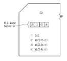
MLC 모드 선택기(210)는 플래시 메모리(230)의 동작 방식(SLC 방식 또는 MLC 방식)을 선택한다. MLC 모드 선택기(210)는 도 5에 도시된 바와 같이 메모리 카드의 외부에 설치될 수도 있고, 도 6에 도시된 바와 같이 컴퓨터에 연결된 마우스 또는 키보드일 수도 있다.The
도 5를 참조하면, SD 카드는 카드 외부에 MLC 모드 선택기를 갖는다. MLC 모드 선택기는 버튼 형식으로 구현될 수도 있고, 쓰기 방지기(Write Protector)와 같이 스위치 형식으로 구현될 수도 있다. 도 5에서는 버튼 형식으로 구현된 MLC 모드 선택기를 보여주고 있다.Referring to Figure 5, the SD card has an MLC mode selector outside the card. The MLC mode selector may be implemented in the form of a button, or may be implemented in the form of a switch, such as a write protector. 5 shows an MLC mode selector implemented in a button form.
예를 들면, 1번 버튼을 누르면 SLC 방식으로 동작하고, 2번 버튼을 누르면 2비트 MLC 방식으로 동작하고, 3번 버튼을 누르면 3비트 MLC 방식으로 동작하고, 4번 버튼을 누르면 4비트 MLC 방식으로 동작한다. 한편, 도 5는 예로서 SD 카드를 보여주고 있지만, 본 발명은 그 이외의 다른 카드(예를 들면, MMC, xD 카드 등)에도 동일하게 적용될 수 있다.For example,
도 6을 참조하면, 어느 파일(06175937)을 이동식 저장 매체(예를 들면, SD 카드)에 복사하고 할 때, 사용자는 마우스나 키보드 등의 입력 장치를 사용하여 이동식 저장매체의 프로그램 방식을 선택할 수 있다.Referring to FIG. 6, when a file (06175937) is copied to a removable storage medium (for example, an SD card), a user may select a program method of the removable storage medium by using an input device such as a mouse or a keyboard. have.
다시 도 4를 참조하면, 사용자(user)는 MLC 모드 선택기(210)를 사용하여, 플래시 메모리(230)의 SLC 방식 또는 MLC 방식을 선택할 수 있다. MLC 방식에는 하나의 메모리 셀이 2비트를 저장할 수 있는 2비트 MLC 방식, 3비트를 저장할 수 있는 3비트 MLC 방식, 그리고 4비트를 저장할 수 있는 4비트 MLC 방식 등이 있다.Referring back to FIG. 4, the user may select the SLC method or the MLC method of the
MLC 모드 선택기(210)는 사용자(user)의 동작 방식 선택에 응답하여, 모드 신호(MOD)를 발생한다. 모드 신호(MOD)는 제어 유닛(221)으로 제공된다. 제어 유닛(221)은 모드 신호(MOD)에 따라, 플래시 메모리(230)가 SLC 방식 또는 MLC 방식으로 동작하도록 한다.The
메모리 컨트롤러(220)는 플래시 메모리(230)의 제반 동작(예를 들면, 쓰기 또는 읽기 동작)을 제어한다. 도 4를 참조하면, 메모리 컨트롤러(220)는 제어 유닛(221) 및 버퍼 메모리(222)를 포함한다. 제어 유닛(221)은 입력된 커맨드에 따라 버퍼 메모리(222) 및 플래시 메모리(230)를 제어한다. 한편, 제어 유닛(221)은 MLC 모드 선택기(210)로부터 모드 신호(MOD)를 입력받고, 플래시 메모리(230)의 프로그램 방식을 제어한다.The
버퍼 메모리(222)는 플래시 메모리(230)에 쓰일 데이터 또는 플래시 메모리(230)로부터 읽은 데이터를 임시로 저장하는 데 사용된다. 버퍼 메모리(222)에 저장된 데이터는 제어 유닛(221)의 제어에 의해 플래시 메모리(230) 또는 호스트(도시되지 않음)로 전송된다. 버퍼 메모리(222)는 랜덤 액세스 메모리(RAM), 예를 들면, SRAM이나 DRAM 등으로 구현될 수 있다.The
계속해서 도 4를 참조하면, 플래시 메모리(230)는 셀 어레이(231), 디코더(232), 페이지 버퍼(233), 비트 라인 선택 회로(234), 데이터 버퍼(235), 그리고 제어 유닛(236)을 구비한다. 도 4에서는 예로서 낸드 플래시 메모리가 도시되어 있다.4, the
셀 어레이(231)는 복수의 메모리 블록(도시되지 않음)으로 구성된다. 각각의 메모리 블록은 복수의 페이지(예를 들면, 32 pages, 64 pages)로 구성되며, 각각의 페이지는 하나의 워드 라인(WL)을 공유하는 복수의 메모리 셀(예를 들면, 512B, 2KB)로 구성된다. 낸드 플래시 메모리의 경우에, 소거 동작은 메모리 블록 단위로 수행되며, 읽기 및 쓰기 동작은 페이지 단위로 수행된다.The
도 2 및 도 3을 참조하면, 하나의 메모리 셀에 2비트 데이터를 저장하는 경우에, 각각의 메모리 셀은 문턱 전압 분포에 따라 4개의 상태(state) 또는 레벨(level)을 갖는다. 이하에서는 하나의 멀티 레벨 셀에 2비트 데이터가 저장되는 경우에 대해 설명한다. 그러나 본 발명은 하나의 멀티 레벨 셀에 2비트 이상의 데이터(예를 들면, 3비트 또는 4비트)가 저장되는 경우에 대해서도 동일하게 적용될 수 있다.2 and 3, in the case of storing 2-bit data in one memory cell, each memory cell has four states or levels according to threshold voltage distributions. Hereinafter, a case where 2-bit data is stored in one multi-level cell will be described. However, the present invention can be equally applied to a case in which two or more bits of data (for example, three bits or four bits) are stored in one multi-level cell.
한편, 각각의 페이지는 모드 신호(MOD)에 따라 SLC 방식 또는 MLC 방식으로 동작한다. 이때 하나의 페이지 내의 메모리 셀들은 모드 신호(MOD)에 따라 싱글 비트 데이터를 저장하거나, 멀티 비트 데이터(예를 들면, 2비트)를 저장하게 된다. 하나의 페이지는 MLC 모드 셀을 포함한다. 도 4에서, 선택 페이지(page0)에는 하나의 MLC 모드 셀(흑색으로 표시됨)이 포함되어 있다. MLC 모드 셀은 선택 페이지(page0)의 프로그램 방식, 즉 SLC 방식 또는 MLC 방식에 대한 정보를 저장한다.Meanwhile, each page operates in the SLC method or the MLC method according to the mode signal MOD. In this case, the memory cells in one page may store single bit data or multi bit data (for example, 2 bits) according to the mode signal MOD. One page includes an MLC mode cell. In FIG. 4, the selection page page0 includes one MLC mode cell (shown in black). The MLC mode cell stores information about a program method of the selection page page0, that is, an SLC method or an MLC method.
일반적으로 셀 어레이(231)는 데이터 필드(data field)와 스페어 필드(spare field)로 구분된다. 하나의 페이지 사이즈가 528B라고 할 때, 512B는 데이터 필드에 해당하고, 16B는 스페어 필드에 해당한다. MLC 모드 셀은 스페어 필드에 포함된다. 플래시 메모리(230)는 프로그램 동작 시에, 선택 페이지(page0)의 프로그램 방식을 스페어 필드 내의 MLC 모드 셀에 저장한다. 플래시 메모리(230)는 읽기 동작 시에, MLC 모드 셀에 저장된 프로그램 방식에 따라 SLC 방식 또는 MLC 방식으로 읽기 동작을 수행한다.In general, the
디코더(232)는 워드 라인(WL0~WLn)을 통해 셀 어레이(231)와 연결되며, 제어 유닛(236)에 의해 제어된다. 디코더(232)는 메모리 컨트롤러(220)로부터 어드레스(ADDR)를 입력받고, 하나의 워드 라인(예를 들면, WL0)을 선택하거나, 비트 라인(BL)을 선택하도록 선택 신호(Yi)를 발생한다. 페이지 버퍼(233)는 비트 라 인(BL0~BLm)을 통해 셀 어레이(231)와 연결된다.The
페이지 버퍼(233)는 버퍼 메모리(222)로부터 로드(load)된 데이터를 저장한다. 페이지 버퍼(233)에는 한 페이지 분량의 데이터가 로드되며, 로드된 데이터는 프로그램 동작 시에 선택 페이지(예를 들면, page0)에 동시에 프로그램된다. 반대로, 페이지 버퍼(233)는 읽기 동작 시에 선택 페이지(page0)로부터 데이터를 읽고, 읽은 데이터를 임시로 저장한다. 페이지 버퍼(233)에 저장된 데이터는 읽기 인에이블 신호(nRE, 도시되지 않음)에 응답하여 버퍼 메모리(222)로 전송된다.The
비트 라인 선택회로(234)는 선택 신호(Yi)에 응답하여 비트 라인을 선택하기 위한 회로이다. 데이터 버퍼(235)는 메모리 컨트롤러(220)와 플래시 메모리(230) 사이의 데이터 전송에 사용되는 입출력용 버퍼이다. 제어 유닛(236)은 메모리 컨트롤러(220)로부터 제어 신호를 입력받고, 플래시 메모리(230)의 내부 동작을 제어하기 위한 회로이다.The bit
본 발명의 제 1 실시 예에 따른 메모리 시스템(200)은 MLC 모드 선택기(210)를 구비한다. MLC 모드 선택기(210)는 사용자(user)의 선택에 응답하여, 모드 신호(MOD)를 발생한다. 제어 유닛(221)은 모드 신호(MOD)에 따라 플래시 메모리(230)가 SLC 방식 또는 MLC 방식으로 프로그램되도록 한다. 플래시 메모리(230)는 프로그램 동작 시에 선택 페이지(page0)의 스페어 필드에 프로그램 방식(SLC 방식 또는 MLC 방식)을 저장하고, 읽기 동작 시에 저장된 방식에 따라 읽기 동작을 수행한다.The
본 발명은 사용자의 선택에 따라 SLC 방식 또는 MLC 방식으로 데이터를 저장할 수 있다. 본 발명에 의하면, 사용자는 데이터의 크기(size) 또는 보안 성(security) 등에 따라 프로그램 속도를 빠르게 할 수 있을 뿐만 아니라 데이터 에러를 줄일 수 있다.The present invention can store data in the SLC method or the MLC method according to a user's selection. According to the present invention, the user can not only increase the program speed according to the size or security of the data, but also reduce the data error.
도 7은 본 발명에 따른 메모리 시스템의 제 2 실시 예를 보여주는 블록도이다. 도 7을 참조하면, 본 발명에 따른 메모리 시스템(300)은 MLC 모드 선택기(310), 메모리 컨트롤러(320), 그리고 플래시 메모리(330)를 포함한다. 메모리 컨트롤러(320)는 제어 유닛(321) 및 버퍼 메모리(322)를 포함한다. 이들 구성 요소들에 동작 설명은 도 4에서 설명한 바와 같다.7 is a block diagram illustrating a second embodiment of a memory system according to the present invention. Referring to FIG. 7, the
도 7을 참조하면, 셀 어레이(231)는 복수의 메모리 블록(BLK0~BLKn, BLKn')으로 구성된다. 각각의 메모리 블록은 복수의 페이지(도시되지 않음)로 구성된다. 각각의 페이지는 모드 신호(MOD)에 따라 SLC 방식 또는 MLC 방식으로 동작한다. 이때 하나의 페이지 내의 메모리 셀들은 모드 신호(MOD)에 따라 싱글 비트 데이터를 저장하거나, 멀티 비트 데이터(예를 들면, 2비트)를 저장한다.Referring to FIG. 7, the
복수의 메모리 블록 중 하나(BLKn')는 MLC 모드 셀을 포함한다. 플래시 메모리(330)의 프로그램 방식은 각 페이지의 스페어 필드에 저장되지 않고, 특정 메모리 블록(BLKn')에 저장된다. 즉, 플래시 메모리(330)는 선택 페이지(도 4 참조, page0)의 프로그램 방식(SLC 방식 또는 MLC 방식)에 대한 모든 정보를 특정 메모리 블록(BLKn')에 저장한다. 그리고 플래시 메모리(330)는 읽기 동작 시에, 특정 메모리 블록(BLKn')에 저장된 프로그램 방식에 따라 SLC 방식 또는 MLC 방식으로 읽기 동작을 수행한다.One of the plurality of memory blocks BLKn 'includes an MLC mode cell. The program method of the
도 8은 본 발명에 따른 메모리 시스템의 제 3 실시 예를 보여주는 블록도이 다. 도 8을 참조하면, 본 발명에 따른 메모리 시스템(400)은 MLC 모드 선택기(410), 메모리 컨트롤러(420), 그리고 플래시 메모리(430)를 포함한다. 메모리 컨트롤러(420)는 제어 유닛(421) 및 버퍼 메모리(422)를 포함한다.8 is a block diagram illustrating a third embodiment of a memory system according to the present invention. Referring to FIG. 8, a
도 8을 참조하면, 제어 유닛(421)은 MLC 모드 저장장치(425)를 포함한다. MLC 모드 저장장치(425)는 플래시 메모리(430)의 프로그램 방식(SLC 방식 또는 MLC 방식)을 저장한다. 즉, 메모리 컨트롤러(420)는 선택 페이지(page0)의 프로그램 방식(SLC 방식 또는 MLC 방식)에 대한 정보를 제어 유닛(421) 내의 MLC 모드 저장장치(425)에 저장한다. 그리고 메모리 컨트롤러(420)는 읽기 동작 시에, MLC 모드 저장장치(425)에 저장된 프로그램 방식에 따라 SLC 방식 또는 MLC 방식으로 플래시 메모리(430)의 읽기 동작을 수행한다. MLC 모드 저장장치(425)는 레지스터, EEPROM 등으로 구현될 수 있다.Referring to FIG. 8, the
이상에서 살펴 본 바와 같이, 본 발명은 사용자의 선택에 따라 플래시 메모리의 프로그램 방식을 결정한다. 본 발명에 의하면, 사용자는 데이터의 특성(사이즈나 중요도 등)에 따라, SLC 방식을 선택함으로 프로그램 속도를 빠르게 할 수 있을 뿐만 아니라 데이터 에러를 줄일 수 있고, MLC 방식을 선택함으로 데이터 용량을 증가할 수 있다.As described above, the present invention determines a program method of a flash memory according to a user's selection. According to the present invention, according to the characteristics of the data (size, importance, etc.), the user can not only increase the program speed by selecting the SLC method but also reduce the data error, and increase the data capacity by selecting the MLC method. Can be.
본 발명은 도면에 도시된 일 실시 예를 참고로 설명되었으나, 이는 예시적인 것에 불과하며, 본 기술 분야의 통상의 지식을 가진 자라면 이로부터 다양한 변형 및 균등한 타 실시 예가 가능하다는 점을 이해할 것이다. 따라서, 본 발명의 진정한 기술적 보호 범위는 첨부된 등록청구범위의 기술적 사항에 의해 정해져야 할 것 이다.Although the present invention has been described with reference to one embodiment shown in the drawings, this is merely exemplary and will be understood by those skilled in the art that various modifications and equivalent other embodiments are possible. . Therefore, the true technical protection scope of the present invention will be defined by the technical details of the appended claims.
본 발명에 따른 메모리 시스템에 의하면, 사용자는 플래시 메모리의 프로그램 방식을 손쉽게 선택할 수 있다. 사용자는 데이터의 특성(사이즈나 중요도 등)에 따라, SLC 방식을 선택함으로 프로그램 속도를 빠르게 할 수 있을 뿐만 아니라 데이터 에러를 줄일 수 있고, MLC 방식을 선택함으로 데이터 용량을 증가할 수 있다.According to the memory system according to the present invention, the user can easily select a program method of the flash memory. The user can not only increase the program speed by selecting the SLC method according to the characteristics of the data (size, importance, etc.), but also reduce the data error, and increase the data capacity by selecting the MLC method.
Claims (21)
Translated fromKoreanPriority Applications (3)
| Application Number | Priority Date | Filing Date | Title |
|---|---|---|---|
| KR1020070005252AKR100875539B1 (en) | 2007-01-17 | 2007-01-17 | Programmable memory system |
| US11/838,348US20080172520A1 (en) | 2007-01-17 | 2007-08-14 | Nonvolatile memory devices including multiple user-selectable program modes and related methods of operation |
| CNA2008100951459ACN101266835A (en) | 2007-01-17 | 2008-01-17 | Non-volatile memory device including multiple user-selectable programming modes and related method |
Applications Claiming Priority (1)
| Application Number | Priority Date | Filing Date | Title |
|---|---|---|---|
| KR1020070005252AKR100875539B1 (en) | 2007-01-17 | 2007-01-17 | Programmable memory system |
Publications (2)
| Publication Number | Publication Date |
|---|---|
| KR20080067834A KR20080067834A (en) | 2008-07-22 |
| KR100875539B1true KR100875539B1 (en) | 2008-12-26 |
Family
ID=39618643
Family Applications (1)
| Application Number | Title | Priority Date | Filing Date |
|---|---|---|---|
| KR1020070005252AExpired - Fee RelatedKR100875539B1 (en) | 2007-01-17 | 2007-01-17 | Programmable memory system |
Country Status (3)
| Country | Link |
|---|---|
| US (1) | US20080172520A1 (en) |
| KR (1) | KR100875539B1 (en) |
| CN (1) | CN101266835A (en) |
Cited By (5)
| Publication number | Priority date | Publication date | Assignee | Title |
|---|---|---|---|---|
| KR101044015B1 (en) | 2009-04-08 | 2011-06-24 | 주식회사 하이닉스반도체 | How Nonvolatile Memory Devices Work |
| KR20170017036A (en)* | 2015-08-04 | 2017-02-15 | 에스케이하이닉스 주식회사 | Data storage device and operating method thereof |
| US9728264B2 (en) | 2015-02-27 | 2017-08-08 | SK Hynix Inc. | Nonvolatile memory device, operating method thereof, and data storage device including the same |
| US9959938B2 (en) | 2015-03-31 | 2018-05-01 | SK Hynix Inc. | Semiconductor memory device outputting status fail signal and operating method thereof |
| US11853601B2 (en) | 2021-01-26 | 2023-12-26 | SK Hynix Inc. | Nonvolatile memory device supporting protection mode and memory system including the same |
Families Citing this family (49)
| Publication number | Priority date | Publication date | Assignee | Title |
|---|---|---|---|---|
| US7269708B2 (en)* | 2004-04-20 | 2007-09-11 | Rambus Inc. | Memory controller for non-homogenous memory system |
| US7852654B2 (en)* | 2006-12-28 | 2010-12-14 | Hynix Semiconductor Inc. | Semiconductor memory device, and multi-chip package and method of operating the same |
| US8429358B2 (en) | 2007-08-14 | 2013-04-23 | Samsung Electronics Co., Ltd. | Method and data storage device for processing commands |
| TWI416524B (en)* | 2008-06-25 | 2013-11-21 | Silicon Motion Inc | Memory device and data storing method |
| US8250247B2 (en) | 2008-08-06 | 2012-08-21 | Sandisk Il Ltd. | Storage device for mounting to a host |
| US8266503B2 (en) | 2009-03-13 | 2012-09-11 | Fusion-Io | Apparatus, system, and method for using multi-level cell storage in a single-level cell mode |
| US8261158B2 (en) | 2009-03-13 | 2012-09-04 | Fusion-Io, Inc. | Apparatus, system, and method for using multi-level cell solid-state storage as single level cell solid-state storage |
| US8135903B1 (en)* | 2009-10-30 | 2012-03-13 | Western Digital Technologies, Inc. | Non-volatile semiconductor memory compressing data to improve performance |
| WO2011058390A1 (en)* | 2009-11-11 | 2011-05-19 | Nokia Corporation | Method and apparatus for information storing |
| US8850128B2 (en)* | 2009-12-23 | 2014-09-30 | HGST Netherlands B.V. | Implementing data storage and dual port, dual-element storage device |
| US8854882B2 (en) | 2010-01-27 | 2014-10-07 | Intelligent Intellectual Property Holdings 2 Llc | Configuring storage cells |
| US8661184B2 (en) | 2010-01-27 | 2014-02-25 | Fusion-Io, Inc. | Managing non-volatile media |
| US9245653B2 (en) | 2010-03-15 | 2016-01-26 | Intelligent Intellectual Property Holdings 2 Llc | Reduced level cell mode for non-volatile memory |
| JP5066241B2 (en)* | 2010-09-24 | 2012-11-07 | 株式会社東芝 | Memory system |
| KR101800444B1 (en) | 2011-03-28 | 2017-12-20 | 삼성전자주식회사 | Control method of nonvolatile memory and memory system including the same |
| JP2013025845A (en)* | 2011-07-21 | 2013-02-04 | Toshiba Information Systems (Japan) Corp | Nonvolatile semiconductor memory device |
| KR101813182B1 (en) | 2011-11-16 | 2017-12-29 | 삼성전자주식회사 | Multi-valued logic device having nonvolatile memory device |
| KR101895605B1 (en) | 2011-11-21 | 2018-10-25 | 삼성전자주식회사 | Flash memory device and program method thereof |
| KR101391352B1 (en)* | 2011-12-19 | 2014-05-07 | 삼성전자주식회사 | Memory system and programming method thereof |
| US9348741B1 (en) | 2011-12-19 | 2016-05-24 | Western Digital Technologies, Inc. | Systems and methods for handling write data access requests in data storage devices |
| US20130339603A1 (en)* | 2011-12-23 | 2013-12-19 | Feng Zhu | Method, apparatus and system for determining access to a memory array |
| US8804452B2 (en) | 2012-07-31 | 2014-08-12 | Micron Technology, Inc. | Data interleaving module |
| KR20140033964A (en)* | 2012-09-11 | 2014-03-19 | 삼성전자주식회사 | Device and method for saving data in terminal |
| KR20140035769A (en)* | 2012-09-14 | 2014-03-24 | 삼성전자주식회사 | Methods and devices of processing continuous shooting image data |
| US8995184B2 (en) | 2012-12-06 | 2015-03-31 | Sandisk Technologies Inc. | Adaptive operation of multi level cell memory |
| US8954655B2 (en)* | 2013-01-14 | 2015-02-10 | Western Digital Technologies, Inc. | Systems and methods of configuring a mode of operation in a solid-state memory |
| KR102053953B1 (en)* | 2013-02-04 | 2019-12-11 | 삼성전자주식회사 | Memory system comprising nonvolatile memory device and program method thereof |
| CN104217762B (en)* | 2013-05-31 | 2017-11-24 | 慧荣科技股份有限公司 | Data storage device and error correction method and data reading method thereof |
| KR102070667B1 (en)* | 2013-08-26 | 2020-01-29 | 삼성전자주식회사 | Method of operating a nonvolatile memory device |
| US10008250B2 (en)* | 2015-03-27 | 2018-06-26 | Intel Corporation | Single level cell write buffering for multiple level cell non-volatile memory |
| US10096355B2 (en)* | 2015-09-01 | 2018-10-09 | Sandisk Technologies Llc | Dynamic management of programming states to improve endurance |
| US9530491B1 (en)* | 2015-11-16 | 2016-12-27 | Sandisk Technologies Llc | System and method for direct write to MLC memory |
| TWI603193B (en)* | 2016-03-31 | 2017-10-21 | 慧榮科技股份有限公司 | Data storage device and data maintenance method thereof |
| KR20190064033A (en)* | 2017-11-30 | 2019-06-10 | 에스케이하이닉스 주식회사 | Memory controller, memory system having the same and operating method thereof |
| US20200004446A1 (en)* | 2018-06-29 | 2020-01-02 | David Aaron Palmer | Multi-level cell data load optimization |
| CN109491592B (en)* | 2018-09-20 | 2022-11-15 | 中山市江波龙电子有限公司 | Storage device, data writing method thereof and storage device |
| KR20200052150A (en)* | 2018-11-06 | 2020-05-14 | 에스케이하이닉스 주식회사 | Memory system and operating method thereof |
| CN111240578B (en)* | 2018-11-28 | 2023-10-10 | 深圳市江波龙电子股份有限公司 | Multi-bit storage device and electronic equipment |
| CN111241028B (en)* | 2018-11-28 | 2025-09-30 | 杭州知存算力科技有限公司 | A digital-analog hybrid storage and computing integrated chip and computing device |
| CN109979508A (en)* | 2019-03-15 | 2019-07-05 | 合肥沛睿微电子股份有限公司 | Ssd apparatus and relevant solid state hard disk control circuit |
| KR102743222B1 (en) | 2019-06-12 | 2024-12-17 | 삼성전자 주식회사 | Electronic device and method of utilizing storage space thereof |
| KR102817611B1 (en)* | 2019-08-02 | 2025-06-11 | 삼성전자주식회사 | Memory device including a plurality of buffer area for supporting fast write and fast read and storage device including the same |
| US11188261B2 (en) | 2019-11-18 | 2021-11-30 | International Business Machines Corporation | Memory controllers for solid-state storage devices |
| US11314427B2 (en)* | 2020-08-21 | 2022-04-26 | Micron Technology, Inc. | Memory device with enhanced data reliability capabilities |
| DE102020123220A1 (en)* | 2020-09-04 | 2022-03-10 | Harman Becker Automotive Systems Gmbh | Storage system, method of operating the same |
| KR20220066601A (en) | 2020-11-16 | 2022-05-24 | 삼성전자주식회사 | Storage device, electronic system including the same storage device and the mehod of operating the same storage device |
| KR20230027957A (en)* | 2021-08-20 | 2023-02-28 | 삼성전자주식회사 | Storage system including host and storage device and operation method thereof |
| US11966626B2 (en)* | 2022-05-13 | 2024-04-23 | Western Digital Technologies, Inc. | Hybrid terabytes written (TBW) storage systems |
| US12254931B2 (en)* | 2022-06-21 | 2025-03-18 | SanDisk Technologies, Inc. | Three-bit-per-cell programming using a four-bit-per-cell programming algorithm |
Citations (2)
| Publication number | Priority date | Publication date | Assignee | Title |
|---|---|---|---|---|
| WO1995034074A1 (en) | 1994-06-02 | 1995-12-14 | Intel Corporation | Dynamic single to multiple bit per cell memory |
| US20050223158A1 (en)* | 2004-04-05 | 2005-10-06 | Sun-Teck See | Flash memory system with a high-speed flash controller |
Family Cites Families (6)
| Publication number | Priority date | Publication date | Assignee | Title |
|---|---|---|---|---|
| US4287570A (en)* | 1979-06-01 | 1981-09-01 | Intel Corporation | Multiple bit read-only memory cell and its sense amplifier |
| US4388702A (en)* | 1981-08-21 | 1983-06-14 | Mostek Corporation | Multi-bit read only memory circuit |
| US5515317A (en)* | 1994-06-02 | 1996-05-07 | Intel Corporation | Addressing modes for a dynamic single bit per cell to multiple bit per cell memory |
| US5594691A (en)* | 1995-02-15 | 1997-01-14 | Intel Corporation | Address transition detection sensing interface for flash memory having multi-bit cells |
| KR100634458B1 (en)* | 2005-07-04 | 2006-10-16 | 삼성전자주식회사 | Flash memory device that performs multi-bit and single-bit program operations with a single page buffer structure |
| KR100732628B1 (en)* | 2005-07-28 | 2007-06-27 | 삼성전자주식회사 | Flash memory device for storing multi-bit data and single-bit data |
- 2007
- 2007-01-17KRKR1020070005252Apatent/KR100875539B1/ennot_activeExpired - Fee Related
- 2007-08-14USUS11/838,348patent/US20080172520A1/ennot_activeAbandoned
- 2008
- 2008-01-17CNCNA2008100951459Apatent/CN101266835A/enactivePending
Patent Citations (2)
| Publication number | Priority date | Publication date | Assignee | Title |
|---|---|---|---|---|
| WO1995034074A1 (en) | 1994-06-02 | 1995-12-14 | Intel Corporation | Dynamic single to multiple bit per cell memory |
| US20050223158A1 (en)* | 2004-04-05 | 2005-10-06 | Sun-Teck See | Flash memory system with a high-speed flash controller |
Cited By (6)
| Publication number | Priority date | Publication date | Assignee | Title |
|---|---|---|---|---|
| KR101044015B1 (en) | 2009-04-08 | 2011-06-24 | 주식회사 하이닉스반도체 | How Nonvolatile Memory Devices Work |
| US9728264B2 (en) | 2015-02-27 | 2017-08-08 | SK Hynix Inc. | Nonvolatile memory device, operating method thereof, and data storage device including the same |
| US9959938B2 (en) | 2015-03-31 | 2018-05-01 | SK Hynix Inc. | Semiconductor memory device outputting status fail signal and operating method thereof |
| KR20170017036A (en)* | 2015-08-04 | 2017-02-15 | 에스케이하이닉스 주식회사 | Data storage device and operating method thereof |
| KR102356523B1 (en)* | 2015-08-04 | 2022-02-03 | 에스케이하이닉스 주식회사 | Data storage device and operating method thereof |
| US11853601B2 (en) | 2021-01-26 | 2023-12-26 | SK Hynix Inc. | Nonvolatile memory device supporting protection mode and memory system including the same |
Also Published As
| Publication number | Publication date |
|---|---|
| US20080172520A1 (en) | 2008-07-17 |
| CN101266835A (en) | 2008-09-17 |
| KR20080067834A (en) | 2008-07-22 |
Similar Documents
| Publication | Publication Date | Title |
|---|---|---|
| KR100875539B1 (en) | Programmable memory system | |
| KR100878479B1 (en) | Memory system that determines program method based on data information | |
| KR100894809B1 (en) | Memory system and its program method | |
| KR100823170B1 (en) | Memory systems and memory cards that use bad blocks in single-level cell mode | |
| US8966163B2 (en) | Non-volatile memory device and method for programming the same | |
| CN103765392B (en) | Wear Leveling of Memory Devices | |
| KR100902008B1 (en) | Memory system including flash memory to store multi-bit data in memory cells | |
| US8082382B2 (en) | Memory device with user configurable density/performance | |
| KR102789095B1 (en) | Storage device and operating method thereof | |
| KR102025251B1 (en) | Nonvolatile memory device and program method | |
| US10902924B2 (en) | Memory system varying pass voltage based on erase count of target memory block and operating method thereof | |
| US7974139B2 (en) | Non-volatile memory generating different read voltages | |
| US8751735B2 (en) | Protection against data corruption for multi-level memory cell (MLC) flash memory | |
| KR20100058166A (en) | Nonvolatile memory device and memory system thereof | |
| KR20120076787A (en) | Method of programming a nonvolatile memory device | |
| KR20110051780A (en) | How to Program Nonvolatile Memory Devices | |
| CN112420109A (en) | Non-volatile memory devices and storage systems | |
| US20250259681A1 (en) | Memory programming using consecutive coarse-fine programming operations of threshold voltage distributions | |
| US20110205792A1 (en) | Memory device reference cell programming method and apparatus | |
| KR102844713B1 (en) | Memory device and operating method thereof | |
| US9728264B2 (en) | Nonvolatile memory device, operating method thereof, and data storage device including the same | |
| US20160322087A1 (en) | Data storage device and operating method thereof | |
| KR20170080759A (en) | Nonvolatile memory device and data storage device including the same | |
| KR102863487B1 (en) | Memory device and operating method thereof | |
| US20160062688A1 (en) | Flash memory device, flash memory system, and operating method |
Legal Events
| Date | Code | Title | Description |
|---|---|---|---|
| A201 | Request for examination | ||
| PA0109 | Patent application | St.27 status event code:A-0-1-A10-A12-nap-PA0109 | |
| PA0201 | Request for examination | St.27 status event code:A-1-2-D10-D11-exm-PA0201 | |
| D13-X000 | Search requested | St.27 status event code:A-1-2-D10-D13-srh-X000 | |
| D14-X000 | Search report completed | St.27 status event code:A-1-2-D10-D14-srh-X000 | |
| E902 | Notification of reason for refusal | ||
| PE0902 | Notice of grounds for rejection | St.27 status event code:A-1-2-D10-D21-exm-PE0902 | |
| P11-X000 | Amendment of application requested | St.27 status event code:A-2-2-P10-P11-nap-X000 | |
| P13-X000 | Application amended | St.27 status event code:A-2-2-P10-P13-nap-X000 | |
| PG1501 | Laying open of application | St.27 status event code:A-1-1-Q10-Q12-nap-PG1501 | |
| E701 | Decision to grant or registration of patent right | ||
| PE0701 | Decision of registration | St.27 status event code:A-1-2-D10-D22-exm-PE0701 | |
| GRNT | Written decision to grant | ||
| PR0701 | Registration of establishment | St.27 status event code:A-2-4-F10-F11-exm-PR0701 | |
| PR1002 | Payment of registration fee | St.27 status event code:A-2-2-U10-U11-oth-PR1002 Fee payment year number:1 | |
| PG1601 | Publication of registration | St.27 status event code:A-4-4-Q10-Q13-nap-PG1601 | |
| PR1001 | Payment of annual fee | St.27 status event code:A-4-4-U10-U11-oth-PR1001 Fee payment year number:4 | |
| R18-X000 | Changes to party contact information recorded | St.27 status event code:A-5-5-R10-R18-oth-X000 | |
| FPAY | Annual fee payment | Payment date:20121130 Year of fee payment:5 | |
| PR1001 | Payment of annual fee | St.27 status event code:A-4-4-U10-U11-oth-PR1001 Fee payment year number:5 | |
| FPAY | Annual fee payment | Payment date:20131129 Year of fee payment:6 | |
| PR1001 | Payment of annual fee | St.27 status event code:A-4-4-U10-U11-oth-PR1001 Fee payment year number:6 | |
| LAPS | Lapse due to unpaid annual fee | ||
| PC1903 | Unpaid annual fee | St.27 status event code:A-4-4-U10-U13-oth-PC1903 Not in force date:20141217 Payment event data comment text:Termination Category : DEFAULT_OF_REGISTRATION_FEE | |
| PC1903 | Unpaid annual fee | St.27 status event code:N-4-6-H10-H13-oth-PC1903 Ip right cessation event data comment text:Termination Category : DEFAULT_OF_REGISTRATION_FEE Not in force date:20141217 |