KR100874662B1 - Continuous vapor deposition system - Google Patents
Continuous vapor deposition systemDownload PDFInfo
- Publication number
- KR100874662B1 KR100874662B1KR1020020028781AKR20020028781AKR100874662B1KR 100874662 B1KR100874662 B1KR 100874662B1KR 1020020028781 AKR1020020028781 AKR 1020020028781AKR 20020028781 AKR20020028781 AKR 20020028781AKR 100874662 B1KR100874662 B1KR 100874662B1
- Authority
- KR
- South Korea
- Prior art keywords
- vapor deposition
- substrate
- containers
- continuous
- container
- Prior art date
- Legal status (The legal status is an assumption and is not a legal conclusion. Google has not performed a legal analysis and makes no representation as to the accuracy of the status listed.)
- Expired - Lifetime
Links
Images


Classifications
- C—CHEMISTRY; METALLURGY
- C23—COATING METALLIC MATERIAL; COATING MATERIAL WITH METALLIC MATERIAL; CHEMICAL SURFACE TREATMENT; DIFFUSION TREATMENT OF METALLIC MATERIAL; COATING BY VACUUM EVAPORATION, BY SPUTTERING, BY ION IMPLANTATION OR BY CHEMICAL VAPOUR DEPOSITION, IN GENERAL; INHIBITING CORROSION OF METALLIC MATERIAL OR INCRUSTATION IN GENERAL
- C23C—COATING METALLIC MATERIAL; COATING MATERIAL WITH METALLIC MATERIAL; SURFACE TREATMENT OF METALLIC MATERIAL BY DIFFUSION INTO THE SURFACE, BY CHEMICAL CONVERSION OR SUBSTITUTION; COATING BY VACUUM EVAPORATION, BY SPUTTERING, BY ION IMPLANTATION OR BY CHEMICAL VAPOUR DEPOSITION, IN GENERAL
- C23C14/00—Coating by vacuum evaporation, by sputtering or by ion implantation of the coating forming material
- C23C14/22—Coating by vacuum evaporation, by sputtering or by ion implantation of the coating forming material characterised by the process of coating
- C23C14/56—Apparatus specially adapted for continuous coating; Arrangements for maintaining the vacuum, e.g. vacuum locks
- C23C14/568—Transferring the substrates through a series of coating stations
- C—CHEMISTRY; METALLURGY
- C23—COATING METALLIC MATERIAL; COATING MATERIAL WITH METALLIC MATERIAL; CHEMICAL SURFACE TREATMENT; DIFFUSION TREATMENT OF METALLIC MATERIAL; COATING BY VACUUM EVAPORATION, BY SPUTTERING, BY ION IMPLANTATION OR BY CHEMICAL VAPOUR DEPOSITION, IN GENERAL; INHIBITING CORROSION OF METALLIC MATERIAL OR INCRUSTATION IN GENERAL
- C23C—COATING METALLIC MATERIAL; COATING MATERIAL WITH METALLIC MATERIAL; SURFACE TREATMENT OF METALLIC MATERIAL BY DIFFUSION INTO THE SURFACE, BY CHEMICAL CONVERSION OR SUBSTITUTION; COATING BY VACUUM EVAPORATION, BY SPUTTERING, BY ION IMPLANTATION OR BY CHEMICAL VAPOUR DEPOSITION, IN GENERAL
- C23C14/00—Coating by vacuum evaporation, by sputtering or by ion implantation of the coating forming material
- C23C14/06—Coating by vacuum evaporation, by sputtering or by ion implantation of the coating forming material characterised by the coating material
- C23C14/12—Organic material
- C—CHEMISTRY; METALLURGY
- C23—COATING METALLIC MATERIAL; COATING MATERIAL WITH METALLIC MATERIAL; CHEMICAL SURFACE TREATMENT; DIFFUSION TREATMENT OF METALLIC MATERIAL; COATING BY VACUUM EVAPORATION, BY SPUTTERING, BY ION IMPLANTATION OR BY CHEMICAL VAPOUR DEPOSITION, IN GENERAL; INHIBITING CORROSION OF METALLIC MATERIAL OR INCRUSTATION IN GENERAL
- C23C—COATING METALLIC MATERIAL; COATING MATERIAL WITH METALLIC MATERIAL; SURFACE TREATMENT OF METALLIC MATERIAL BY DIFFUSION INTO THE SURFACE, BY CHEMICAL CONVERSION OR SUBSTITUTION; COATING BY VACUUM EVAPORATION, BY SPUTTERING, BY ION IMPLANTATION OR BY CHEMICAL VAPOUR DEPOSITION, IN GENERAL
- C23C14/00—Coating by vacuum evaporation, by sputtering or by ion implantation of the coating forming material
- C23C14/22—Coating by vacuum evaporation, by sputtering or by ion implantation of the coating forming material characterised by the process of coating
- C23C14/24—Vacuum evaporation
- C23C14/243—Crucibles for source material
- H—ELECTRICITY
- H10—SEMICONDUCTOR DEVICES; ELECTRIC SOLID-STATE DEVICES NOT OTHERWISE PROVIDED FOR
- H10K—ORGANIC ELECTRIC SOLID-STATE DEVICES
- H10K71/00—Manufacture or treatment specially adapted for the organic devices covered by this subclass
- H10K71/10—Deposition of organic active material
- H10K71/16—Deposition of organic active material using physical vapour deposition [PVD], e.g. vacuum deposition or sputtering
- H10K71/164—Deposition of organic active material using physical vapour deposition [PVD], e.g. vacuum deposition or sputtering using vacuum deposition
- H—ELECTRICITY
- H10—SEMICONDUCTOR DEVICES; ELECTRIC SOLID-STATE DEVICES NOT OTHERWISE PROVIDED FOR
- H10K—ORGANIC ELECTRIC SOLID-STATE DEVICES
- H10K50/00—Organic light-emitting devices
- H10K50/10—OLEDs or polymer light-emitting diodes [PLED]
- H10K50/11—OLEDs or polymer light-emitting diodes [PLED] characterised by the electroluminescent [EL] layers
- H—ELECTRICITY
- H10—SEMICONDUCTOR DEVICES; ELECTRIC SOLID-STATE DEVICES NOT OTHERWISE PROVIDED FOR
- H10K—ORGANIC ELECTRIC SOLID-STATE DEVICES
- H10K85/00—Organic materials used in the body or electrodes of devices covered by this subclass
- H10K85/60—Organic compounds having low molecular weight
- H—ELECTRICITY
- H10—SEMICONDUCTOR DEVICES; ELECTRIC SOLID-STATE DEVICES NOT OTHERWISE PROVIDED FOR
- H10K—ORGANIC ELECTRIC SOLID-STATE DEVICES
- H10K85/00—Organic materials used in the body or electrodes of devices covered by this subclass
- H10K85/60—Organic compounds having low molecular weight
- H10K85/615—Polycyclic condensed aromatic hydrocarbons, e.g. anthracene
- H—ELECTRICITY
- H10—SEMICONDUCTOR DEVICES; ELECTRIC SOLID-STATE DEVICES NOT OTHERWISE PROVIDED FOR
- H10K—ORGANIC ELECTRIC SOLID-STATE DEVICES
- H10K85/00—Organic materials used in the body or electrodes of devices covered by this subclass
- H10K85/60—Organic compounds having low molecular weight
- H10K85/631—Amine compounds having at least two aryl rest on at least one amine-nitrogen atom, e.g. triphenylamine
Landscapes
- Chemical & Material Sciences (AREA)
- Engineering & Computer Science (AREA)
- Chemical Kinetics & Catalysis (AREA)
- Materials Engineering (AREA)
- Mechanical Engineering (AREA)
- Metallurgy (AREA)
- Organic Chemistry (AREA)
- Manufacturing & Machinery (AREA)
- Physical Vapour Deposition (AREA)
- Electroluminescent Light Sources (AREA)
Abstract
Translated fromKoreanDescription
Translated fromKorean본 발명은 아래에 첨부된 도면들을 참조하여 상세하게 설명될 것이다.The invention will be described in detail with reference to the accompanying drawings below.
도 1은 본 발명에 의한 연속기상증착시스템의 실시예의 전체적인 측면도,1 is an overall side view of an embodiment of a continuous vapor deposition system according to the present invention;
도 2는 도 1에서 보여진 연속기상증착시스템의 기본적인 부분을 나타낸 사시도,Figure 2 is a perspective view showing the basic part of the continuous vapor deposition system shown in FIG.
도 3은 기판들의 반송을 위한 반송 장치의 기본적인 부분의 부분단면도,3 is a partial cross-sectional view of a basic part of a conveying apparatus for conveying substrates;
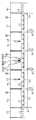
도 4a,4b 및 4c는 도 1에서 보여진 연속기상증착시스템에 제공된 크루서블의 예들과, 거기에 형성된 격벽들의 구조적 예들을 나타낸 평면도들,4A, 4B and 4C are plan views showing examples of crucibles provided in the continuous vapor deposition system shown in FIG. 1 and structural examples of partition walls formed therein;
도 5는 도 4a에서 보여진 크루서블의 사시도,Figure 5 is a perspective view of the crucible shown in Figure 4a,
도 6은 도 4a에서 VI-VI라인을 따라서 취해진 도 4a에서 보여진 크루서블의 단면도, 및6 is a cross-sectional view of the crucible shown in FIG. 4A taken along line VI-VI in FIG. 4A, and
도 7은 크루서블의 경사진 종단면도.7 is an inclined longitudinal sectional view of the crucible;
<도면의 주요부분에 대한 부호의 설명><Description of the symbols for the main parts of the drawings>
1 : 연속기상증착시스템10 : 기판홀더1: continuous vapor deposition system 10: substrate holder
10a:사각개구 11 : 반송롤러10a: square opening 11: conveying roller
19 : 게이트20 : 유리기판19: gate 20: glass substrate
20a : 기상증착영역 21 : 크루서블20a: vapor deposition area 21: crucible
22 : 기상증착재료23 : 열선22: vapor deposition material 23: hot wire
24 : 수직판26 : 원호홈24: vertical plate 26: arc groove
27 : 나사못28 : 더블도어셔트27: screw 28: double door shutter
28a : 피벗29 : 수냉식재킷28a: pivot 29: water-cooled jacket
본 발명은 다른 기상증착재료들이 기판 위에서 얇은 층들을 연속형성하기에 적당한 연속기상증착장치에 관한 것이다. 또한 본 발명은 기상증착장치와 기상증착방법에 관한 것이다.The present invention relates to a continuous vapor deposition apparatus in which other vapor deposition materials are suitable for continuously forming thin layers on a substrate. The present invention also relates to a vapor deposition apparatus and a vapor deposition method.
대표적인 유기EL소자는 일반적으로 ITO(Indium tin oxide)유리기판 위에 진공증착에 의해서 연속적으로 형성된 정공수송층, 발광층, 전자수송층 및 전극층을 가지고 있다. 유리기판 위에 그러한 연속층들을 형성하기 위한 종래의 연속기상증착장치에는, 유리기판 위에 다른 기상증착재료들을 증착시키기 위한 복수개의 진공증착실(기판저장실과 예비처리실을 포함한다)은 중앙의 진공운송로봇실에 대하여 방사형으로 배치되어 있고, 그 결과 유리기판은 유리기판 위에 다른 재료들의 얇은 층들을 형성하기 위한 중앙의 진공운송로봇실의 로봇 장치를 통하여 복수의 진공증착실들 중에서 하나의 실로부터 다른 실으로 연속적으로 통과한다.Representative organic EL devices generally have a hole transport layer, a light emitting layer, an electron transport layer and an electrode layer continuously formed by vacuum deposition on an indium tin oxide (ITO) glass substrate. In a conventional continuous vapor deposition apparatus for forming such continuous layers on a glass substrate, a plurality of vacuum deposition chambers (including a substrate storage chamber and a pretreatment chamber) for depositing different vapor deposition materials on the glass substrate have a central vacuum transport robot. Radially with respect to the chamber, with the result that the glass substrate is separated from one of the plurality of vacuum deposition chambers via a robotic device of a central vacuum transport robot chamber for forming thin layers of different materials on the glass substrate. Pass continuously.
그러한 종래의 연속기상증착장치에서, 기판은 중앙의 진공운송로봇실를 통하 여 복수개의 진공증착실들 사이에서 하나의 챔버로부터 다른 실로 옮길 필요가 있고, 이는 시간을 소모하고 비효율적인 작업이다. 게다가, 기상증착재료들은 진공증착실들이 중앙의 진공운송로봇실 주위에 단순히 배열되어 있는 종래 장치의 기본적인 구조 때문에 과도하게 낭비된다. 명확히 말하면, 그러한 종래의 연속기상증착장치에서, 다른 기상증착재료들과 기판은 각각 진공증착실안의 하부 및 상부영역들 에 배열되어 있고, 자신의 축에 대해 자전하고 기판의 한 면 위에 다른 기상증착재료들의 층들을 실질적으로 고른 층두께로 전체적으로 형성하기 위해 기판이 중앙의 진공운송로봇실의 축 주위로 공전하는 동안에 다른 기상증착재료들은 증발되도록(혹은 승화되도록) 가열된다. 그러나, 기상증착재료들의 과도한 낭비는, 층들의 평평함이 크루스블이나 보트로부터 모든 방향에서 위쪽으로 넓게 확산되며 각각이 근사적으로 점증발원으로 간주되는 증발 분자들의 일부를 기판위에 증착하는 것에 의해서만 보장되기 때문에 피할 수 없다. 다시 말하면 기상증착재료들의 과도한 낭비는 증발된 분자들의 대부분이 기상증착실의 내벽 위에 증착되고 단지 증발된 분자들의 몇 퍼센트만이 실제로 기판 위에 증착되기 때문에 피할 수 없다. 유기EL소자들의 생산에 사용되는 약간의 기상증착재료들은 과도하게 비싼데 예를 들어 그램당 수 만엔 정도이다. 따라서, 기상증착재료들의 과도한 낭비는 생산비의 실질적인 증가를 야기시킨다.In such conventional continuous vapor deposition apparatus, the substrate needs to be moved from one chamber to another between a plurality of vacuum deposition chambers through a central vacuum transport robot chamber, which is a time consuming and inefficient operation. In addition, vapor deposition materials are excessively wasted due to the basic structure of the conventional apparatus in which the vacuum deposition chambers are simply arranged around a central vacuum transport robot chamber. To clarify, in such conventional continuous vapor deposition apparatus, different vapor deposition materials and substrates are arranged in the lower and upper regions of the vacuum deposition chamber, respectively, rotating about their axis and other vapor deposition on one side of the substrate. Other vapor deposition materials are heated to evaporate (or sublime) while the substrate revolves around the axis of the central vacuum transport robot chamber to form layers of materials substantially at substantially even layer thickness. However, excessive waste of vapor deposition materials is ensured only by depositing on the substrate a portion of the evaporation molecules, the flatness of the layers spreading wide in all directions upwards from the crumbble or boat, each of which is considered to be an evaporation source. Because it is inevitable. In other words, excessive waste of vapor deposition materials is inevitable because most of the vaporized molecules are deposited on the inner wall of the vapor deposition chamber and only a few percent of the vaporized molecules are actually deposited on the substrate. Some vapor deposition materials used in the production of organic EL devices are excessively expensive, for example tens of thousands of grams per gram. Therefore, excessive waste of vapor deposition materials causes a substantial increase in production costs.
하나의 유기EL소자에 있어서, 주 재료와 적어도 하나의 도펀트재료는 유기발광층의 발광색을 결정하기 위하여 특정한 비율(예를 들면, 100:1 혹은 100:0.5)로 기판위에 일반적으로 함께 증착된다. 그러나, 종래의 유기EL소자에 있어서, 그러한 다른 재료들 대부분은 낭비되고, 나아가 시간당 특정 비율을 유지하기도 어렵게 된다.In one organic EL element, the main material and at least one dopant material are generally deposited together on the substrate in a specific ratio (e.g., 100: 1 or 100: 0.5) to determine the emission color of the organic light emitting layer. However, in the conventional organic EL device, most of such other materials are wasted, and it is also difficult to maintain a specific ratio per hour.
본 발명은 상술한 문제를 감안하여 고안되었고, 그에 따라서 시간적 효율성과 기상증착재료의 최소한의 낭비로, 연속적으로 기판위에 기상증착재료들의 층을 형성하는 것을 가능하게 하는 기상증착장치를 제공한다.SUMMARY OF THE INVENTION The present invention has been devised in view of the above problems, and thus provides a vapor deposition apparatus which makes it possible to continuously form a layer of vapor deposition materials on a substrate with time efficiency and minimal waste of vapor deposition material.
본 발명은 또한 기판 위에 다른 기상증착재료를 함께 증착하여 특정한 비율에서 그것의 최소한의 변동으로 다른 기상증착재료들의 층들을 형성할 수 있게 하는 기상증착장치를 제공한다.The present invention also provides a vapor deposition apparatus that enables the deposition of other vapor deposition materials together on a substrate to form layers of other vapor deposition materials with its minimal variation at a certain rate.
예를 들면, 본 발명의 한 관점에서, 적어도 하나의 기상증착재료가 가열되고 진공에서 증발되어 기판의 증착되는 영역(이후로 "기상증착영역")위에 증착되는 연속기상증착장치가 제공된다. 이 연속기상증착장치는 기판이 놓인 수평면에 평행하게 운송방향으로 기판을 운송하는 운송기, 운송방향에 일직선으로 놓인 복수개의 기상증착실, 복수개의 기상증착실들 각각에서 기판이 놓인 수평면 아래에 위치한 적어도 하나의 컨테이너, 및 컨테이너를 위해 제공된 가열기를 포함한다.For example, in one aspect of the present invention, there is provided a continuous vapor deposition apparatus in which at least one vapor deposition material is heated and evaporated in vacuo to be deposited over a deposited region of a substrate (hereinafter referred to as a "vapor deposition region"). The continuous vapor deposition apparatus includes a vehicle for transporting a substrate in a transport direction parallel to a horizontal plane on which the substrate is placed, a plurality of vapor deposition chambers arranged in a straight line in the transport direction, and at least below the horizontal plane on which the substrate is placed in each of the plurality of vapor deposition chambers. One container, and a heater provided for the container.
기판의 기상증착영역은 아래로 향하고 있고 운송기의 아래면을 통하여 노출되어 있다. 기상증착실들의 각각은 기판이 운송방향으로 운송되는 공간을 포함한다. 컨테이너는 기상증착재료를 포함하고 그것의 너비는 운송방향에 직각인 방향에서 기상증착영역을 커버한다.The vapor deposition region of the substrate faces downward and is exposed through the underside of the vehicle. Each of the vapor deposition chambers includes a space in which the substrate is transported in the transport direction. The container contains vapor deposition material and its width covers the vapor deposition region in a direction perpendicular to the direction of transport.
기상증착재료를 담기 위한 복수개의 컨테이너들은 복수개의 기상증착실들 중의 적어도 하나에 위치할 수 있다. 복수개의 컨테이너들의 상단개구들은, 복수개의 컨테이너로부터 올라간 각각의 증발된 재료들이 기판의 기상증착영역위의 공통영역에 공증착되도록 운송방향에 대해 직각방향으로 뻗어 있다. The plurality of containers for containing the vapor deposition material may be located in at least one of the plurality of vapor deposition chambers. The top openings of the plurality of containers extend at right angles to the transport direction such that each evaporated material raised from the plurality of containers co-deposits into a common area on the vapor deposition region of the substrate.
복수 개의 컨테이너들 중의 적어도 하나에는 공통영역을 형성하기 위해서 다른 컨테이너들에 대하여 소망하는 각도로 조절할 수 있게 경사져 있다.At least one of the plurality of containers is inclined to be adjustable at a desired angle with respect to other containers to form a common area.
본 발명의 다른 관점에 따르면, 적어도 하나의 기상증착재료가 가열되고, 진공에서 증발되어 기판위의 가상증착영역 위에 증착되는 기상증착장치가 제공된다.According to another aspect of the present invention, there is provided a vapor deposition apparatus in which at least one vapor deposition material is heated, evaporated in vacuo, and deposited on a virtual deposition region on a substrate.
운송기는 기판이 놓인 수평면에 대해 평행한 운송방향으로 기상증착실로 기판을 운송하고, 그 동안에 기상증착영역은 아래를 향해 운송기의 아래면을 통하여노출된다. 컨테이너는 기판이 놓인 수평면 아래에 제공되고 기상증착재료를 포함한다. 컨테이너의 너비는 운송방향에 수직한 방향에서 기상증착영역을 커버한다. 가열기는 기상증착재료의 가열을 위해 컨테이너에 제공된다.The conveyer transports the substrate into the vapor deposition chamber in a transport direction parallel to the horizontal plane on which the substrate is placed, during which the vapor deposition region is exposed through the underside of the conveyer downwards. The container is provided below the horizontal plane on which the substrate is placed and contains vapor deposition material. The width of the container covers the vapor deposition zone in a direction perpendicular to the transport direction. The heater is provided to the container for heating the vapor deposition material.
본 발명의 또 다른 관점에 따르면, 기상증착장치는 독립적인 공증착장치로서 사용될 수 있다. 본 발명의 이러한 면에서, 기상증착실에 제공된 복수개의 컨데이너들은, 복수개의 컨테이너들로부터 올려진 각각의 기상증착재료들이 기판의 기상증착영역 위의 공통영역에 공증착되도록 배열된다. 게다가, 복수개의 컨테이너들 중의 적어도 하나에는 기판의 기상증착영역에서 상기 공통영역을 형성하기 위해서 다른 컨테이너들에 대해서 소망하는 각도로 조절할 수 있게 경사져 있다.According to another aspect of the present invention, the vapor deposition apparatus may be used as an independent co-deposition apparatus. In this aspect of the present invention, the plurality of containers provided in the vapor deposition chamber are arranged such that respective vapor deposition materials raised from the plurality of containers are co-deposited in a common area above the vapor deposition region of the substrate. In addition, at least one of the plurality of containers is inclined so as to be adjustable at a desired angle with respect to other containers to form the common area in the vapor deposition region of the substrate.
컨테이너에 관해서는, 컨테이너의 깊이는 거기에 들어있고 증발되는 기상증착재료가 컨테이너의 깊이방향에서 기판의 기상증착영역 쪽으로 올라갈 수 있도록 결정된다. 이러한 배열에 따르면, 굴뚝효과로 인한 기상증착재료분자들의 지향성을 이용함으로써 기상증착재료가 기판의 기상증착영역으로 증발된다. 그러나, 종래 기술에서는 기상증착영역 위에 평평한 층을 형성하려고 시도할 때, 기상증착재료를 포함하기 위한 컨테이너(크루서블)가 굴뚝효과를 가지도록 설계되는 것은 바람직하지 않다는 것을 알 수 있다.As for the container, the depth of the container is determined so that the vapor deposition material contained therein and evaporated can rise in the vapor deposition region of the substrate in the depth direction of the container. According to this arrangement, the vapor deposition material is evaporated to the vapor deposition region of the substrate by utilizing the directivity of the vapor deposition material molecules due to the chimney effect. However, it can be seen that in the prior art, when attempting to form a flat layer over the vapor deposition region, it is not desirable that the container (crusable) for containing the vapor deposition material is designed to have a chimney effect.
게다가, 컨테이너가 운송방향에 대해 수직한 방향에서 전 기상증착영역을 커버하도록 설계된다면, 단독형 컨테이너나 분리형 컨테이너와 같이 어떤 형태의 컨테이너도 이용될 수 있다.In addition, if the container is designed to cover the entire vapor deposition area in a direction perpendicular to the direction of transport, any type of container, such as a stand alone container or a separate container, may be used.
단독형 컨테이너가 사용되는 경우, 운송방향에 대해 수직한 방향으로 기다란 사각박스의 형상을 가진 컨테이너가 바람직하다. 다시 말하면, 설명처럼 형성된 크루서블은 운송방향에 수직한 방향에서 기상증착영역을 크루서블의 최소길이로써 커버할 수 있다.When a single container is used, a container having a shape of a rectangular box elongated in a direction perpendicular to the transport direction is preferable. In other words, the crucible formed as described can cover the vapor deposition region in the direction perpendicular to the transport direction with the minimum length of the crucible.
더욱이, 기상증착재료를 일정하게 가열하기 위해서는 크루서블의 내부공간이 복수개의 격벽들에 의해서 구획되는 것이 바람직하다. 보다 명확하게는, 기상증착재료의 층이 기상증착영역 위에 균일하게 형성되도록 격벽들을 운송방향에 경사진 방향으로 서로 평행하게 뻗는다. 한편, 그 격벽들이 운송방향에 대해 평행하게 뻗는다면, 열이 기상증착재료에 균일하게 가해질 수 있다는 상황에서도, 격벽들 바로 위의 기상증착재료분자들의 밀도는 굴뚝효과 때문에 희박해진다. 복수개의 격벽들은 운송방향에 대해 수직한 방향으로 배열된 복수의 컨테이너들에 상당한다는 것과 기상증착재료가 제공되는 컨테이너가 복수의 컨테이너들로 분리될 수 있다는 것도 이해된다.Further, in order to constantly heat the vapor deposition material, it is preferable that the internal space of the crucible is partitioned by a plurality of partitions. More specifically, the partitions extend parallel to each other in a direction inclined to the transport direction so that the layer of vapor deposition material is formed uniformly above the vapor deposition region. On the other hand, if the partitions extend parallel to the direction of transport, even in the situation where heat can be applied evenly to the vapor deposition material, the density of the vapor deposition material molecules directly above the partitions becomes thin due to the chimney effect. It is understood that the plurality of partitions correspond to a plurality of containers arranged in a direction perpendicular to the transport direction, and that a container provided with vapor deposition material can be separated into a plurality of containers.
추가적인 관점으로서의 본 발명은 적어도 하나의 기상증착재료가 가열되고 진공에서 증발되어 기판의 기상증착영역위에 증착 기상증착방법에 적용될 수 있다. 이 기상증착방법은 다음 단계를 포함한다:As a further aspect of the present invention, at least one vapor deposition material may be heated and evaporated in vacuo to be applied to the deposition vapor deposition method over a vapor deposition region of a substrate. This vapor deposition method includes the following steps:
기상증착영역은 아래로 향하고 운송기의 아래면에 있는 개구를 통하여 노출되면서, 기판이 놓인 수평면에 평행한 운송방향에서 적어도 하나의 기상증착실의 내부공간으로 기판을 운송하는 단계;Transporting the substrate into the interior space of the at least one vapor deposition chamber in a transport direction parallel to the horizontal plane on which the substrate is placed, with the vapor deposition region facing down and exposed through an opening in the underside of the vehicle;
기상증착실의 내부공간에서, 기상증착재료를 포함하며 기상증착실의 내부 공간에 있고 운송방향에 수직한 방향으로 기상증착영역을 커버하는 너비를 가진 적어도 하나의 컨테이너 위에 기판을 위치시키는 단계; 및Positioning the substrate on at least one container in the interior space of the vapor deposition chamber, the substrate comprising a vapor deposition material and having a width in the interior space of the vapor deposition chamber and covering the vapor deposition region in a direction perpendicular to the transport direction; And
기상증착영역 위의 기상증착재료를 증발시키기 위해 컨테이너를 가열하는 단계.Heating the container to evaporate the vapor deposition material above the vapor deposition zone.
상술한 기상증착방법에 있어서, 복수개의 기상증착실들은 증착되는 기판이 운송되는 운송방향에 제공될 수 있다. 컨테이너는 기상증착실 각각에 위치하고, 가열기는 거기에 포함된 기상증착재료를 증발시키기 위해 기상증착실들의 각각에 형성될 수 있다.In the above vapor deposition method, a plurality of vapor deposition chambers may be provided in a transport direction in which a substrate to be deposited is transported. A container is located in each of the vapor deposition chambers, and a heater may be formed in each of the vapor deposition chambers to evaporate the vapor deposition material contained therein.
상술한 기상증착방법에 있어서, 복수의 컨테이너들은 기상증착실에 제공될 수 있다. 각각의 컨테이너들에는 다른 기상증착재료들이 제공된다. 각 컨테이너는 다른 기상증착재료들이 증발될 수 있도록 독립적으로 가열된다.In the above vapor deposition method, a plurality of containers may be provided in the vapor deposition chamber. Each container is provided with different vapor deposition materials. Each container is heated independently to allow other vapor deposition materials to evaporate.
본 발명에 따른 연속기상증착장치, 기상증착장치 또는 기상증착방법에 사용되는 기상증착재료들은 그것들이 가열 작용을 통해서 증발될 수 있기만 하면 어떤 기상증착재료도 될 수 있다. 그런 기상증착재료는, 예를 들면, 유기EL소자, 유기태양전지나 유기FET(field effect transistor)의 층들의 형성을 위해 사용된 어떠한 기능성유기막층형성재료일 수 있다. 또한 그러한 기상증착재료들은 예를 들면, 철, 혹은 산화물(oxide), 질화물(nitride), 탄화물(carbide)이나 할로겐화물(halogenide)과 같은 어떤 공지의 무기합성재료일 수 있다. 유기EL소자의 발광층이나 전자수송층의 전형적인 유기재료들은 트리스(8-히드록시퀴놀린) 알루미늄 착화합물(보통 "Alq3"라 함)을 포함한다. 유기EL소자의 정공수송층의 대표적인 유기물질들은 N,N'-디페닐-N,N'-비스(3-메틸페닐)-1,1'-디페닐-4,4'-디아민(보통 "TPD"라 함)과 같은 아릴라민 화합물을 포함한다.The vapor deposition materials used in the continuous vapor deposition apparatus, the vapor deposition apparatus or the vapor deposition method according to the present invention may be any vapor deposition material as long as they can be evaporated through a heating action. Such vapor deposition material may be, for example, any functional organic film layer forming material used for forming layers of an organic EL element, an organic solar cell or an organic field effect transistor (FET). Such vapor deposition materials may also be any known inorganic synthetic materials such as, for example, iron or oxides, nitrides, carbides or halides. Typical organic materials of the light emitting layer or the electron transporting layer of the organic EL device include tris (8-hydroxyquinoline) aluminum complex compound (commonly referred to as "Alq3 "). Representative organic materials of the hole transport layer of the organic EL device are N, N'-diphenyl-N, N'-bis (3-methylphenyl) -1,1'-diphenyl-4,4'-diamine (usually "TPD"). Ararylamine compounds).
한편, 유기EL소자로 사용되는 전형적인 무기재료들은 할로겐화금속(metal halide)과 같은 무기합성물들을 포함하고, 또한 주로 전극을 위한 재료로서 사용되는 알루미늄, 마그네슘 및 은을 포함한다. 본 발명은 기상증착재료에 관한 것이 아니고, 따라서, 유기EL소자의 층들의 형성을 위해 사용되는 유기 또는 무기물질의 다른 예들이 여기서는 개시되지 않았다는 것을 알아야 한다.On the other hand, typical inorganic materials used for organic EL devices include inorganic compounds such as metal halides, and also include aluminum, magnesium and silver mainly used as materials for electrodes. It is to be understood that the present invention does not relate to vapor deposition materials and therefore that other examples of organic or inorganic materials used for the formation of the layers of the organic EL element are not disclosed herein.
<실시예><Example>
도 1은 본 발명에 따른 연속기상증착시스템의 실시예를 보여주고 있다. 연속기상증착시스템(1)은 복수개의 기판홀더(10)와 도 1에서 보듯이 기판홀더(10)를 오른쪽에서 왼쪽으로 운반하는 운송롤러(11)을 구비한다. 복수개의 기판홀더(10)와 복수개의 운송롤러(11)가 운송기를 구성한다. 복수개의 운송롤러들(11)은 모터(미도시)에 의해서 구동된다. 연속기상증착시스템(1)는 기판홀더들(10)의 운송방향(도 1에서 보여진 좌향수평방향; 이후에는 "운송방향"으로서 고려됨)으로, 도 1에서 보듯이 오른쪽에서 왼쪽의 순서로, 준비스테이지(12), 예비진공실(13), 제1기상증착실(14), 제2기상증착실(공증착실)(15), 제3기상증착실(16), 예비방출실(17) 및 방출스테이지(18)를 구비한다. 각 챔버(13 내지 17)는 반송방향으로 운송되는 기판홀더(10)가 통과하는 공간(운송공간)을 포함하고, 챔버안의 진공이 대응하는 게이트(19)에 의해 다른 챔버들에 독립적으로 제어될 수 있도록 구획되어 있다. 즉, 연속기상증착시스템은 각 챔버들(13내지 17)의 각각을 위한 진공펌프(P)를 가지고 있어, 각 챔버(13 내지 17)내의 진공의 정도가 대응된 진공펌프(P)로 제어될 수 있다. 각 게이트(19)는 운송방향으로 이전의 챔버(혹은 스테이지)에서 다음 챔버(혹은 스테이지)로 기판홀더(10)를 운송하는 동안에만 열도록 제어될 수 있다. 다르게는, 각 게이트(19)는, 기판홀더(10)에 의해서 고정된 기판들(도 1에서는 보이지 않음)이 대량 생산을 위해 연속적으로 운송된다면, 모든 시간에서 열려진 채로 남을 수 있다. 종래의 기술은 각 챔버들(13 내지 17)의 구성과 작동을 위해서 사용되었다. 연속기상증착시스템은 바람직하게는 청정실에 마련된다.1 shows an embodiment of a continuous vapor deposition system according to the present invention. The continuous
도 2 및 3에서 보듯이, 각 기판홀더(10)에는 그것의 중심에 사각 개구(10a)가 마련되어 있고, 또 그것의 바닥 위에 운송방향으로 서로 평행하게 뻗어 있는 한 쌍의 V 홈들(10b)이 마련된다. 도 3에서 보듯이, 유리기판(20)은 개구(10a)를 통하 여 기판홀더(10)의 아래쪽으로 열려있는(노출된) 유리기판(20)의 기상증착되는 하나의 영역(20a)(이후로 "기상증착영역")을 가지게끔 기판홀더(10)에 올려져 있다. 기상증착영역(20a)은 개구(10a)에 의해서 운송방향으로 길이 X를 가지고 운송방향과 직각방향으로 너비 Y를 가지는 사각지역으로 규정된다. 하나의 유리기판(20)이 설명되는 실시예에서 하나의 기판홀더(10)위에 올려져 있지만, 하나 이상의 유리기판(20)이 유리기판(20)의 크기에 따라 하나의 기판홀더(10)위에 올려질 수 있다. 2 and 3, each
따라서, 운송롤러(11)들이 구동될 때, 기상증착영역(20a)이 개구(10a)를 통하여 대응된 기판홀더(10)의 아래면으로 노출되는 유리 기판(20)은, 그 사이에 놓인 챔버들(13, 14, 15 및 17)을 통하여 순차적으로 준비스테이지(12)로부터 방출스테이지(18)로 운송된다.Therefore, when the
기상증착영역(20a)의 크기가 새도우마스크(보이지 않는)에 의해서 규정되는 것이 필요하다면, 새도우마스크는 기판홀더(10)와 일체로 형성될 수 있다.If the size of the
도 1에서 보인 예시적인 실시예에서, 연속기상증착시스템은 기판홀더(10)들이 놓인 수평면 아래의 제1 및 제3증착실들(14 및 16)의 각각에, 컨테이너(크루서블)(21)를 포함하고 있다. 연속기상증착시스템은, 제2기상증착실(공증착실)(15)에, 세 개의 크루서블들(21)(21A, 21B 및 21C)을 포함한다. 이러한 다섯 개의 크루서블들(21)은 기본적으로 같은 구조를 가지고 있으며, 각 크루서블(21)은 운송방향에 대해 수직한 방향으로 기다란 사각박스의 형상이다. 설명한 것처럼 크루서블(21)을 형성하는 것은, 기상증착영역(20a)이 운송방향에 수직한 방향에서 크루서블(21)의 최소 길이(너비)로 커버될 수 있기 때문에 이점이 있다. 다시 말하면, 크루서블(21)이 위의 이점을 가지도록 설계되는 한, 그것의 형상이나 배향과 같은 크루서블(21)의 다른 요소들은 약간의 자유도를 가지게 된다.In the exemplary embodiment shown in FIG. 1, the continuous vapor deposition system has a container (crusable) 21 in each of the first and
각 크루서블(21)은 운송방향에 수직한 방향에서 그것의 내부길이(21Y)(도 2, 4a 및 6참조)가 기상증착영역(20a)의 너비(Y)보다 약간 크게 되도록 설계된다. 즉, 내부길이(21Y)는 크루서블(21)이 운송방향에 대해 수직한방향에서 기상증착영역(20a)(너비 Y)을 완전하게 덮도록 결정된다.Each
게다가, 각 크루서블(21)의 깊이(21Z)(도 6 및 7 참조)는, 가열에 의해 증착되도록 크루서블(21)에 포함돼 있는 기상증착재료(22)가 크루서블(21)내의 깊이(21Z)방향에서 효율적으로 기상영역쪽으로 올라갈 수 있도록 결정된다. 다시 말하면, 이 배열은 증착재료(22)에 굴뚝효과(chimney effect)를 얻게 한다. 마찬가지로, 굴뚝효과를 얻기 위해서 크루서블(21)내에 포함된 기상증착재료(22)의 양은 작게 설정된다. 각 크루서블(21)의 내부너비(21X)는 바람직하게는 기상증착영역(20a)위에 형성된 층이 운송방향으로 평탄하지 않게 되지 않도록 내부길이(21Y) 및 깊이(21Z)의 각각보다 작도록 결정된다.In addition, the
각 크루서블(21)의 내부공간은 복수개의 격벽들(21P)로써 나눠진다. 도 4a, 4b 및 4c는 각 크루서블(21)의 내부공간을 구획하는 방법의 다른 예들을 보여준다. 격벽들(21P)은 크루서블(21)내에 있는 기상증착재료(22)에 균일하게 열을 가하여 기상증착재료(22)를 일정하게 증착시키기 위해 각 크루서블(21)내에 형성된다. 격벽들(21P)은 서로 평행하게 뻗어 있지만 운송방향으로 평행하게 뻗어 있지는 않다. 즉, 격벽들(21P)은 운송방향에 대해 경사진 방향으로 서로 평행하게 뻗어 있다. 이 격벽들(21P)의 경사진 배열은, 기상증착영역(20a)위의 각 지점이 각 크루서블(21)의 적어도 하나의 격벽을 지나 그곳으로부터 올라간 증발된 재료가 기상증착영역(20a)위에 확실하게 증착되도록 할 수 있기 때문에, 기상증착영역(20a)위에 기상증착재료의 층을 균일하게 형성하는 데 이롭다. 그러므로, 격벽들(21P)의 경사각과 그것들 사이의 간격은 기상증착재료의 층이 균일하게 형성되도록 결정된다. 각 크루서블(21)은, 그것의 격벽들(21P)과 함께, 바람직하게는 탄소와 같은 고열전도재(예를 들면, 적어도 1W/m*K의 열전도도를 가진 재료)로 만들어진다.The inner space of each
각 크루서블(21)에 포함된 기상증착재료(22)는 각 크루서블(21)내의 격벽들 사이에 동일하게 분배되도록 정교하게 계량된다. 기상증착재료(22)가 각 크루서블(21)내의 격벽들 사이에 동일하게 분배되지 않는다면, 각 구획으로부터 증발된 기상증착재료의 분자들의 밀도는, 증발된 기상증착재료(22)의 온도 분포가 운송방향의 수직한 방향 즉, 내부길이(21Y)의 방향에서 고르게 되더라도, 시간이 가면 평탄하게되지 않는다. 이것은 전체 기상증착영역(20a)에서 기상증착재료층의 균일성을 보장하는 것을 어렵게 만든다. 도 2 및 7에서 보듯이, 연속기상증착시스템은 각 크루서블(21)주위로 가열장치로서 소용되는 약간의 필라멘트(열선)를 구비한다. 각 크루서블(21)의 온도는 필라멘트(23)에 인가되는 전류를 조절함으로서 제어될 수 있다.The
제1및 제3기상증착실(14 및 16)에 있는 두 크루서블들(21)의 각각은 한 쌍의 정지된 수직판(24)에 그것들 사이에 수직하게 유지되게 고정돼 있다. 명확히 말하면, 각 크루서블(21)의 중심면이 깊이(21Z)방향으로 크루서블(21)의 내부너비(21X)의 중심을 통과하는 면으로서 정의된다면, 두 크루서블들(21)의 각각은 중심면이 수평방향으로 운송되는 유리기판들(20)의 기상증착영역(20a)에 수직한 방향으로 뻗어 있도록 대응되는 두 수직판들(24)의 쌍에 고정되어 있다. 한편, 제 2기상증착실(15)(공증착실)에 제공된 나머지 세 개의 크루서블들(21)(21A, 21B 및 21C)을 고려하면, 세 개의 크루서블들(21)(21A, 21B 및 21C)로부터 올라간 각각의 증발된 재료들이 각 유리기판(20)의 기상증착영역(20a)위의 공통영역에 함께 증착 되도록, 세 개의 크루서블들(21)(21A, 21B 및 21C)의 각각의 사각형상단개구들은 운송방향에 수직한 방향으로 뻗어 있다. 특히, 중앙의 크루서블(21B)은 제1 및 제3기상증착실들(14 및 16)에 제공된 두 크루서블(21) 각각의 그것과 비슷한 방법으로 한 쌍의 정지된 수직판(24)(24B)에서 그것들 사이에 수직으로 유지되게 고정되어 있는 반면에, 다른 두 크루서블(21)(21A 및 21C)은 운송방향에 수직한 방향으로 뻗어 있는 샤프트(25)에 대해 회전할 수 있도록 한 쌍의 정지된 수직판들(24)(24A 혹은 24B)사이에 고정되어 있어, 중앙 크루서블(21B)과 관련해서 두 크루서블(21A 및 21C) 각각의 경사각은 샤프트(25)에 대해 조절 가능하다. 크루서블(21A)을 지지하는 두 개의 정지된 수직판(24A)중의 하나는 관련된 샤프트(25)에 주위에 뻗어 있는 원호홈(26)을 구비하고, 크루서블(21A)은 원호홈(26)을 통과하여 크루서블속에 나사식으로 고정되는 고정나사못(27)을 구비하고 있다(도 1 및 7 참조). 비슷하게, 크루서블(21C)을 지지하는 두 개의 정지된 수직판(24C)중의 하나는 관련된 샤프트(25)주위로 뻗어 있는 원호홈(26)을 구비하고 있고, 반면에 크루서블(21C)은 원호홈(26)을 통과하여 크루서블(21C)에 나사식으로 고정되는 고정나사못(27)을 구비한다 (도 1 및 7 참조). 따라서, 두 크루서블(21A 및 21C)의 각도조절구조들은 각 유리기판(20)의 기상증착영역(20a)의 공통영역 위에 세 개의 크루서블들(21A,21B 및 21C)로부터 올라간 각각의 증발된 재료들을 공증착하는 것을 가능하게 만든다. 실제로, 중앙 크루서블(21B)에 대해서 두 개의 크루서블들(21A 및 21C)의 개별 각도들은, 바람직하게는 두 크루서블들(21A 및 21C) 각각의 중심면이 주어진 유리기판(20)의 기상증착영역(20a)위의 일직선에 선 중앙 크루서블(21B)의 중심면과 교차하도록 조절된다. 중앙 크루서블(21B)에 대해서 두 개의 크루서블들(21A 및 21C)의 이상적인 각도는 실험에 의해서 쉽게 결정될 수 있다.Each of the two
도 7에서 보듯이, 연속기상증착시스템은 각 크루서블(21)의 상부에 크루서블(21)의 상부를 열고 닫기 위한 더블도어셔트(28)를 포함하고 있고, 그리고/또는 각 크루서블(21)의 주위에 수냉식 재킷(29)을 포함 한다. 더블도어셔트(28)와 수냉식재킷(29)은 도 7에서 보여진다. 더블도어셔트(28)는 크루서블(21)의 상부를 열고 닫기 위해 대응하는 추축(28a)에 각각 피벗된 한 쌍의 셔트플레이트를 구비한다. 예를 들면, 더블도어셔트(28)는 관련된 크루서블(21)(기상증착재료(22))의 온도가 기설정된 온도에 도달할 때, 그리고 유리기판(20)이 관련된 크루서블(21)위에 위치되도록 운송된 때 열리고, 셔트(28)는 다른 모든 시간에 닫힌다. 수냉식 재킷(29)은 패널(29a)과 크루서블(21)사이에 기 설정된 틈을 가지고서 크루서블(21)을 둘러싸는 패널(29a)을 구비하며, 또 패널(29a)의 내부표면위에는 크루서블(21)의 온도가 상승할 때 시스템(1)의 주변 요소들에 대한 크루서블(21)로부터의 열의 방사효과를 최소화하기 위해 냉각수가 돌아다니는 냉각 튜브(29b)를 구비한다. 수냉식 재킷(29)은 관련된 크루서블(21)(기상증착재료(22))의 온도를 제어하기 위한 온도제어기로서 사용하기 위해 필라멘트(23)와 함께 사용될 수 있다. 시장에서 입수할 수 있는 막두께인식모니터와 제어기는, 크루서블(21)위에 위치한 유리기판(20)의 기상증착영역(20a)과 겹치지 않기 위해서 각 크루서블(21)의 상부 끝에 제공될 수 있다. 이러한 배열 때문에, 필라멘트(23)에 인가된 전류의 값은 막두께검출모니터와 이것을 위한 제어기에 의해서 제어될 수 있고, 그 결과 소망의 휘망하는 축적 속도가 기상증착영역(20a)위에 기상증착재료(22)의 증착하는 공정 동안 축적속도를 모니터링 함으로써 얻어진다.As shown in FIG. 7, the continuous vapor deposition system includes a
상술한 구조를 가진 연속기상증착시스템은 아래의 방식으로 적색광을 발산하는 유기전계발광 소자들을 생산하기 위한 시스템으로서 사용될 수 있다.The continuous vapor deposition system having the above-described structure can be used as a system for producing organic electroluminescent elements emitting red light in the following manner.
만들어진 투명전극(ITO는 양극으로 소용)이 그 위에 미리 형성되어 있는 ITO 유리기판들이 유리기판들(20)로 사용되며;ITO glass substrates on which a transparent electrode (ITO is used as an anode) made in advance are used as the
유기EL소자의 정공수송층의 재료로서 소용되는 TPD가 제 1기상증착실(14)의 크루서블(21)에 제공되며;TPD, which serves as a material for the hole transport layer of the organic EL element, is provided in the
발광층의 주 재료로서 사용되는 Alq3제2기상증착실(15)의 중앙 크루서블(21)에 제공되며;A
노랑색용을 위한 도펀트로서 소용되는 루브렌(rubrene)이 제 2기상증착실(15)의 크루서블(21)에 제공되며; 그리고Rubrene serving as a dopant for yellow color is provided in the
적색용을 위한 도펀트로서 소용되는 DCM2가 제 2기상증착실(15)의 크루서블(21)에 제공된다.DCM2, which serves as a dopant for red color, is provided in the
적색광 발광 재료로서 소용되는 DCM2가 광을 효율적으로 방출하게 할 목적으로, 루브렌은 주재료로서 소용되는 Alq3로부터 발생된 여기에너지를 DCM2로 부드럽게 전송하기 위한 보조도펀트로서 사용된 한다. 이 때, 제2기상증착실(공증착실)에 있는 크루서블들(21A, 21B 및 21C)의 온도는, 각 크루서블들(21A, 21B 및 21C)에 각각 들어있는 앞서 말한 루브렌, Alq3 및 DCM2가 각 유리기판(20)의 기상증착영역(20a)위에 소망하는 혼합비로 함께 증착되기 위해 증발되도록 서로 독립적으로 제어된다. 전자 운송층으로서 소용되는 Alq3는 제3기상증착실(16)의 크루서블(21)에 제공된다.In order to make DCM2, which serves as a red light emitting material, efficiently emit light, rubrene is used as an auxiliary dopant for smoothly transferring excitation energy generated from Alq3, which is used as a main material, to DCM2. At this time, the temperatures of the
이러한 기상증착재료들이 다섯 개의 크루서블(21)에 포함된 후에, 층을 형성하는 작업(기상증착작업)은 아래의 방식으로 수행된다.After these vapor deposition materials are included in the five
맨 처음에, 각 예비진공실(13), 제1내지 제3기상증착실들(14, 15 및 16) 및 예비방출실(17)의 각각은 기 설정된 진공도에 비워지고 개개의 크루서블은 미리 기 설정된 온도로 가열된다. 이 상태에서, 기판홀더들(10)위에 올려진 각 유리기판들(20)은 올라간 증발된 재료(TPD)가 기상증착영역(20a)위에 증착되어 정공수송층을 형성하도록 우선적으로 제 1기상증착실(14)로 옮겨진다.Initially, each of the
이어서, 정공수송층이 그 위에 형성된 유리기판(20)은 제2기상증착실로 옮겨 져 그로부터 올라온 세 개의 증발된 재료들(루브렌, Alq3 및 DCM2)이 기상증착영역(20a)에 공증착되어 정공수송층위에 발광층을 형성한다. 크루서블(21B)로부터의 기상증착재료의 축적속도 및 크루서블(21C)로부터의 기상증착재료의 축적속도에 대한 크루서블(21)로부터 기상증착재료의 축척속도의 비(공증착비)는 크루서블들(21A, 21B 및 21C)의 가열온도들을 제어함으로써 정교하게 제어될 수 있어 관련된 막두께검출모니터에 의해 모니터된 각 크루서블(21A, 21B 및 21C)로부터의 기상증착재료의 축적속도는 희망하는 속도가 된다.Subsequently, the
또한, 발광층이 형성된 유리기판(20)은 제3기상증착실(16)로 옮겨져 그로부터 올라간 증발된 재료는 기상증착영역(20a)위에 증착되어 전자수송층을 형성한다. 음극으로서 소용되는 전극층과 같은 다른 층들이 각 유리기판(20)위에 형성될 필요가 있다면, 연속기상증착시스템은 단지 하나 혹은 그 이상의 추가적인 기상증착실을 부가하는 것이 필요할 뿐이다.In addition, the
유리기판(20)이 직선모양으로 운송되면서 다른 기상증착재료들의 얇은 층들이 각 유리기판(20)위에 균일하게 공증착되는 본 실시예의 연속기상증착시스템(1)에서, 층두께의 제어는 앞서 언급한 막두께검출모니터에 의해서 검출된 축적속도와 유리기판(20)의 운송속도를 제어함으로써 달성될 수 있다. 이 경우, 층 두께는 유리기판들(20)이 크루서블(21)위에서 왕복운동하도록 의도적으로 유리기판(20)을 앞뒤로 움직임으로써 그리고 유리기판들(20)의 왕복운동의 횟수와 운동속도를 조절함으로써 제어될 수 있다. 이러한 제어는 크루서블들(21)의 꼭대기에 제공된 더블도 어셔트(28)를 사용한 층두께제어와 조합될 수 있다.In the continuous
복수개의 진공증착실들의 중앙에 위치한 중앙의 진공운송로봇실의 로봇장치를 통하여 복수개의 진공증착실 간에 하나의 챔버로부터 다른 챔버로 기판들이 연속적으로 수송되는 종래의 연속기상증착시스템과 달리, 상술한 층형성방법은 다음의 특징을 가진다:Unlike the conventional continuous vapor deposition system in which substrates are continuously transported from one chamber to another chamber between a plurality of vacuum deposition chambers through a robot apparatus of a central vacuum transport robot chamber located at the center of the plurality of vacuum deposition chambers, The layer formation method has the following characteristics:
(1) 기상증착재료들의 층들은 유리기판들(20)이 운송방향으로 운송면서 각 유리기판(20)의 기상증착영역(20a)위에 연속적으로 형성될 수 있고;(1) layers of vapor deposition materials may be formed continuously on the
(2) 각 기상증착재료의 층은, 각각의 완전한 층이 기상증착영역(20a)의 너비(Y)방향(도 2참조)으로 각 유리기판(20)의 기상증착영역(20a)위에 동시에 형성될 수 있기 때문에, 큰 기상증착영역위에서 쉽게 형성될 수 있고;(2) The layers of each vapor deposition material, each complete layer is formed simultaneously on the
(3) 다른 기상증착재료들은 주어진 정확한 비(공증착비)로 다른 기상증착재료들의 층을 형성하기 위해 각 유리기판(20)의 기상증착영역(20a)위에 완전하게 공증착되도록 증발될 수 있고; 그리고(3) Other vapor deposition materials may be evaporated to be completely co-deposited on the
(4) 각 기상증착재료의 층은 기상증착재료의 최소한의 낭비로 각 유리기판(20)의 기상증착영역(20a)위에 형성될 수 있다.(4) A layer of each vapor deposition material may be formed on the
비록 연속기상증착시스템의 상술한 실시예가 복수개의 기상증착실(14, 15 및 16)을 구비하더라도, 제1및 제3기상증착실들(14 및 16)중의 하나에 대응하는 하나의 기상증착실만을 포함하는 기상증착시스템으로 이루어지는 것도 가능하다. 이러한 기상증착시스템에 따르면, 기상증착재료는 기상증착재료의 최소한의 낭비로 각 유리기판(20)의 기상증착영역(20a)위에 증착될 수 있다. 더구나, 제2기상증착실(공 증착실)(15)에 대응하는 하나의 기상증착실만을 포함하는 기상증착시스템으로 이루어지는 것도 가능하다. 이러한 기상증착시스템에 따르면, 다른 기상증착재료들은 공증착비가 정확하게 제어될 수 있으면서 공증착재료들의 최소한의 낭비로 각 유리기판(20)의 기상증착영역(20a)위에 공증착될 수 있다.Although the above-described embodiment of the continuous vapor deposition system includes a plurality of
연속기상증착시스템의 위에서 예시된 실시예에서 ITO 유리기판 위에 다른 유기재료들을 증착하여 ITO 유리기판 위에 정공수송층, 발광층 및 전자수송층은 순차적으로 형성하는 방법이 논의되었다. 음극층은 완성품으로서의 유기EL소자를 제공하기 위해 전극운송층위에 형성될 필요가 있다. 음극층의 재료가 증착된 유리기판의 기상증착영역은 정공수송층, 발광층 및 전자수송층의 유기물질들이 증착된 그것과 일치하지 않기 때문에, 일반적인 경우 유기물질들이 증착된 유리기판의 기상증착영역이 섀도우마스크(혹은 섀도우마스크의 기능과 유리기판이 올려진 기판홀드의 기능을 가지는 부재)에 의해서 규정된다. 섀도우마스크나 이중기능부재를 배치, 제거, 교체 및/또는 포지션닝을 위한 메커니즘은 이 기술분야에서 알려진 것이고, 본 발명의 목적과 관련이 없다. 따라서 전자수송층위에 음극층을 형성하는 공정은 여기서 논의되지 않았다. 음극층은, 음극층의 재료가 증착된 위에서 유리기판의 기상증착영역이 규정된 후에, 유리기판위에 다른 층을 형성하는 상술한 방식과 비슷한 방식으로 전자수송층 위에 형성될 수 있다. 비록 각 크루서블(21)의 내부공간이 운송방향에 경사진 방향으로 뻗어 있는 복수개의 격벽들(21P)에 의해서 구획되었지만, 본 발명은 이 특정한 배열로만 한정되지 않는다. 즉, 복수개의 크루서블들은 운송방향에 수직한 방향으로 배열될 수 있다.In the above-described embodiment of the continuous vapor deposition system, a method of sequentially forming the hole transport layer, the light emitting layer, and the electron transport layer on the ITO glass substrate by depositing other organic materials on the ITO glass substrate has been discussed. The cathode layer needs to be formed on the electrode transport layer to provide an organic EL element as a finished product. The vapor deposition region of the glass substrate on which the material of the cathode layer is deposited does not coincide with that of the organic materials of the hole transport layer, the light emitting layer, and the electron transport layer, so in general, the vapor deposition region of the glass substrate on which the organic materials are deposited is a shadow mask. (Or a member having a function of a shadow mask and a substrate hold on which a glass substrate is placed). Mechanisms for placing, removing, replacing and / or positioning shadowmasks or dual function members are known in the art and are not relevant to the object of the present invention. Therefore, the process of forming the cathode layer on the electron transport layer is not discussed here. The cathode layer may be formed on the electron transport layer in a manner similar to that described above, after the vapor deposition region of the glass substrate is defined on which the material of the cathode layer is deposited, to form another layer on the glass substrate. Although the internal space of each
전술한 바로부터 알 수 있듯이, 본 발명에 따르면, 효율성있게 그리고 기상증착재료들의 최소한의 낭비로 기판위에 기상증착재료들의 층들을 순차적으로 형성할 수 있게 하는 기상증착시스템이 완성된다. 게다가, 기상증착재료의 최소한의 낭비로 기판위에 기상증착재료의 층을 형성할 수 있게 하는 기상증착시스템이 완성된다. 이와 더불어 기판위에 다른 기상증측재료들을 공증착하여 기상증착재료들의 최소한의 낭비로 특정 비율로 다른 기상증착재료의 층들을 기판위에 형성할 수 있게 하는 기상증착시스템도 완성된다.As can be seen from the foregoing, according to the present invention, a vapor deposition system is completed which enables to sequentially form layers of vapor deposition materials on a substrate efficiently and with minimal waste of vapor deposition materials. In addition, a vapor deposition system is completed that allows the formation of a layer of vapor deposition material on a substrate with minimal waste of vapor deposition material. In addition, a vapor deposition system is also completed that allows other vapor deposition materials to be co-deposited on a substrate to form layers of other vapor deposition materials on the substrate at a specific rate with minimal waste of vapor deposition materials.
발명의 주장하는 정신과 범위 내에서 이루어지는 변형과 같은 분명한 변화가 여기서 서술한 본 발명의 특정 실시예에서 만들어질지 모른다. 여기에 포함된 모든 사항은 예가 되는 것이며 본 발명의 범위를 한정하지 않는다는 것을 지적한다.Obvious changes, such as modifications made within the spirit and scope of the invention as claimed, may be made in the specific embodiments of the invention described herein. It is pointed out that all matters contained herein are examples and do not limit the scope of the present invention.
전술한 바로부터 알 수 있듯이, 본 발명에 따르면, 효율성있게 그리고 기상증착재료들의 최소한의 낭비로 기판위에 기상증착재료들의 층들을 순차적으로 형성할 수 있게 하는 기상증착시스템이 완성된다. 게다가, 기상증착재료의 최소한의 낭비로 기판위에 기상증착재료의 층을 형성할 수 있게 하는 기상증착시스템이 완성된다. 이와 더불어 기판위에 다른 기상증측재료들을 공증착하여 기상증착재료들의 최소한의 낭비로 특정 비율로 다른 기상증착재료의 층들을 기판위에 형성할 수 있게 하는 기상증착시스템도 완성된다.As can be seen from the foregoing, according to the present invention, a vapor deposition system is completed which enables to sequentially form layers of vapor deposition materials on a substrate efficiently and with minimal waste of vapor deposition materials. In addition, a vapor deposition system is completed that allows the formation of a layer of vapor deposition material on a substrate with minimal waste of vapor deposition material. In addition, a vapor deposition system is also completed that allows other vapor deposition materials to be co-deposited on a substrate to form layers of other vapor deposition materials on the substrate at a specific rate with minimal waste of vapor deposition materials.
Claims (27)
Translated fromKoreanApplications Claiming Priority (2)
| Application Number | Priority Date | Filing Date | Title |
|---|---|---|---|
| JP2001153367AJP4704605B2 (en) | 2001-05-23 | 2001-05-23 | Continuous vapor deposition apparatus, vapor deposition apparatus and vapor deposition method |
| JPJP-P-2001-00153367 | 2001-05-23 |
Publications (2)
| Publication Number | Publication Date |
|---|---|
| KR20020090156A KR20020090156A (en) | 2002-11-30 |
| KR100874662B1true KR100874662B1 (en) | 2008-12-17 |
Family
ID=18997894
Family Applications (1)
| Application Number | Title | Priority Date | Filing Date |
|---|---|---|---|
| KR1020020028781AExpired - LifetimeKR100874662B1 (en) | 2001-05-23 | 2002-05-23 | Continuous vapor deposition system |
Country Status (5)
| Country | Link |
|---|---|
| US (2) | US7429300B2 (en) |
| EP (1) | EP1260605B1 (en) |
| JP (1) | JP4704605B2 (en) |
| KR (1) | KR100874662B1 (en) |
| TW (1) | TWI261627B (en) |
Cited By (1)
| Publication number | Priority date | Publication date | Assignee | Title |
|---|---|---|---|---|
| WO2010120535A3 (en)* | 2009-03-31 | 2011-02-10 | Soladigm, Inc. | Fabrication of low defectivity electrochromic devices |
Families Citing this family (118)
| Publication number | Priority date | Publication date | Assignee | Title |
|---|---|---|---|---|
| TW490714B (en) | 1999-12-27 | 2002-06-11 | Semiconductor Energy Lab | Film formation apparatus and method for forming a film |
| US8382902B2 (en)* | 2000-04-12 | 2013-02-26 | Seagate Technology Llc | Single disc vapor lubrication |
| US20020011205A1 (en) | 2000-05-02 | 2002-01-31 | Shunpei Yamazaki | Film-forming apparatus, method of cleaning the same, and method of manufacturing a light-emitting device |
| US7517551B2 (en)* | 2000-05-12 | 2009-04-14 | Semiconductor Energy Laboratory Co., Ltd. | Method of manufacturing a light-emitting device |
| US7309269B2 (en) | 2002-04-15 | 2007-12-18 | Semiconductor Energy Laboratory Co., Ltd. | Method of fabricating light-emitting device and apparatus for manufacturing light-emitting device |
| US8900366B2 (en)* | 2002-04-15 | 2014-12-02 | Samsung Display Co., Ltd. | Apparatus for depositing a multilayer coating on discrete sheets |
| US6943066B2 (en)* | 2002-06-05 | 2005-09-13 | Advantech Global, Ltd | Active matrix backplane for controlling controlled elements and method of manufacture thereof |
| DE60305246T2 (en)* | 2002-07-19 | 2006-09-14 | Lg Electronics Inc. | Thermal PVD coating source for organic electroluminescent layers |
| US20040040504A1 (en)* | 2002-08-01 | 2004-03-04 | Semiconductor Energy Laboratory Co., Ltd. | Manufacturing apparatus |
| US20040123804A1 (en)* | 2002-09-20 | 2004-07-01 | Semiconductor Energy Laboratory Co., Ltd. | Fabrication system and manufacturing method of light emitting device |
| US7132016B2 (en)* | 2002-09-26 | 2006-11-07 | Advantech Global, Ltd | System for and method of manufacturing a large-area backplane by use of a small-area shadow mask |
| JP2004227814A (en)* | 2003-01-20 | 2004-08-12 | Korai Kagi Kofun Yugenkoshi | Organic light emitting device and its manufacturing method |
| US7211461B2 (en)* | 2003-02-14 | 2007-05-01 | Semiconductor Energy Laboratory Co., Ltd. | Manufacturing apparatus |
| DE10312641B4 (en)* | 2003-03-21 | 2009-11-12 | Fraunhofer-Gesellschaft zur Förderung der angewandten Forschung e.V. | Method and device for producing an OLED display |
| JP4463492B2 (en)* | 2003-04-10 | 2010-05-19 | 株式会社半導体エネルギー研究所 | Manufacturing equipment |
| JP4493926B2 (en)* | 2003-04-25 | 2010-06-30 | 株式会社半導体エネルギー研究所 | Manufacturing equipment |
| JP4447256B2 (en)* | 2003-06-27 | 2010-04-07 | 株式会社半導体エネルギー研究所 | Method for manufacturing light emitting device |
| JP2005050747A (en)* | 2003-07-31 | 2005-02-24 | Ulvac Japan Ltd | Vapor deposition source, film forming device and film forming method |
| US7153180B2 (en)* | 2003-11-13 | 2006-12-26 | Eastman Kodak Company | Continuous manufacture of flat panel light emitting devices |
| US7232588B2 (en)* | 2004-02-23 | 2007-06-19 | Eastman Kodak Company | Device and method for vaporizing temperature sensitive materials |
| ATE360180T1 (en)* | 2004-03-15 | 2007-05-15 | Applied Materials Gmbh & Co Kg | VACUUM TREATMENT SYSTEM WITH TRANSPORTABLE MAINTENANCE VALVE |
| JP2005285576A (en)* | 2004-03-30 | 2005-10-13 | Mitsubishi-Hitachi Metals Machinery Inc | Manufacturing device of in-line type organic electroluminescent element |
| JP4393402B2 (en)* | 2004-04-22 | 2010-01-06 | キヤノン株式会社 | Organic electronic device manufacturing method and manufacturing apparatus |
| US20050244580A1 (en)* | 2004-04-30 | 2005-11-03 | Eastman Kodak Company | Deposition apparatus for temperature sensitive materials |
| JP4455937B2 (en)* | 2004-06-01 | 2010-04-21 | 東北パイオニア株式会社 | Deposition source, vacuum film formation apparatus, organic EL panel manufacturing method |
| JP2006225757A (en)* | 2005-01-21 | 2006-08-31 | Mitsubishi Heavy Ind Ltd | Vacuum vapor deposition apparatus |
| US7918940B2 (en) | 2005-02-07 | 2011-04-05 | Semes Co., Ltd. | Apparatus for processing substrate |
| KR100671673B1 (en)* | 2005-03-09 | 2007-01-19 | 삼성에스디아이 주식회사 | Multiple vacuum deposition apparatus and control method |
| US7271111B2 (en)* | 2005-06-08 | 2007-09-18 | Advantech Global, Ltd | Shadow mask deposition of materials using reconfigurable shadow masks |
| JP5568729B2 (en)* | 2005-09-06 | 2014-08-13 | 国立大学法人東北大学 | Film forming apparatus and film forming method |
| JP5044223B2 (en)* | 2007-01-10 | 2012-10-10 | パナソニック株式会社 | Vacuum deposition equipment |
| KR100927621B1 (en)* | 2007-03-22 | 2009-11-20 | 삼성에스디아이 주식회사 | Apparatus for depositing a protective film layer, and a deposition method using the same |
| CN101646802B (en)* | 2007-03-30 | 2011-08-03 | 东京毅力科创株式会社 | Evaporation source unit, vapor deposition device, and temperature adjustment device for vapor deposition source unit |
| JP5081516B2 (en)* | 2007-07-12 | 2012-11-28 | 株式会社ジャパンディスプレイイースト | Vapor deposition method and vapor deposition apparatus |
| JP5046882B2 (en) | 2007-11-21 | 2012-10-10 | 三菱重工業株式会社 | In-line deposition system |
| EP2231895B1 (en)* | 2007-12-21 | 2017-10-18 | Advanced Galvanisation AG | Method and devices for controlling a vapour flow in vacuum evaporation |
| US20090176010A1 (en)* | 2008-01-04 | 2009-07-09 | M Zwick Lucy | Method of manufacturing organic light emitting display |
| US9353436B2 (en)* | 2008-03-05 | 2016-05-31 | Applied Materials, Inc. | Coating apparatus with rotation module |
| US20090255467A1 (en)* | 2008-04-15 | 2009-10-15 | Global Solar Energy, Inc. | Apparatus and methods for manufacturing thin-film solar cells |
| WO2009134041A2 (en)* | 2008-04-29 | 2009-11-05 | Sunic System. Ltd. | Evaporator and vacuum deposition apparatus having the same |
| US9782949B2 (en) | 2008-05-30 | 2017-10-10 | Corning Incorporated | Glass laminated articles and layered articles |
| CN102112646A (en)* | 2008-08-05 | 2011-06-29 | 株式会社爱发科 | Vacuum treatment apparatus and vacuum treatment method |
| US20100116208A1 (en)* | 2008-11-13 | 2010-05-13 | Applied Materials, Inc. | Ampoule and delivery system for solid precursors |
| JP5431901B2 (en)* | 2008-12-26 | 2014-03-05 | キヤノンアネルバ株式会社 | Inline vacuum processing apparatus, control method for inline vacuum processing apparatus, and method for manufacturing information recording medium |
| EP2230703A3 (en) | 2009-03-18 | 2012-05-02 | Semiconductor Energy Laboratory Co., Ltd. | Manufacturing apparatus and manufacturing method of lighting device |
| JP5620146B2 (en) | 2009-05-22 | 2014-11-05 | 三星ディスプレイ株式會社Samsung Display Co.,Ltd. | Thin film deposition equipment |
| TWI475124B (en)* | 2009-05-22 | 2015-03-01 | Samsung Display Co Ltd | Thin film deposition apparatus |
| KR101074792B1 (en)* | 2009-06-12 | 2011-10-19 | 삼성모바일디스플레이주식회사 | Thin film deposition apparatus |
| KR101117719B1 (en) | 2009-06-24 | 2012-03-08 | 삼성모바일디스플레이주식회사 | Apparatus for thin layer deposition |
| JP4831841B2 (en)* | 2009-07-10 | 2011-12-07 | 三菱重工業株式会社 | Vacuum deposition apparatus and method |
| KR20110014442A (en) | 2009-08-05 | 2011-02-11 | 삼성모바일디스플레이주식회사 | Thin film deposition apparatus and manufacturing method of organic light emitting display device using the same |
| JP5328726B2 (en)* | 2009-08-25 | 2013-10-30 | 三星ディスプレイ株式會社 | Thin film deposition apparatus and organic light emitting display device manufacturing method using the same |
| JP5611718B2 (en)* | 2009-08-27 | 2014-10-22 | 三星ディスプレイ株式會社Samsung Display Co.,Ltd. | Thin film deposition apparatus and organic light emitting display device manufacturing method using the same |
| JP5677785B2 (en)* | 2009-08-27 | 2015-02-25 | 三星ディスプレイ株式會社Samsung Display Co.,Ltd. | Thin film deposition apparatus and organic light emitting display device manufacturing method using the same |
| US20110052795A1 (en)* | 2009-09-01 | 2011-03-03 | Samsung Mobile Display Co., Ltd. | Thin film deposition apparatus and method of manufacturing organic light-emitting display device by using the same |
| JP5484478B2 (en)* | 2009-10-05 | 2014-05-07 | 東京エレクトロン株式会社 | Film forming apparatus and film forming head |
| US8876975B2 (en) | 2009-10-19 | 2014-11-04 | Samsung Display Co., Ltd. | Thin film deposition apparatus |
| US8481355B2 (en) | 2009-12-15 | 2013-07-09 | Primestar Solar, Inc. | Modular system and process for continuous deposition of a thin film layer on a substrate |
| US8247255B2 (en) | 2009-12-15 | 2012-08-21 | PrimeStar, Inc. | Modular system and process for continuous deposition of a thin film layer on a substrate |
| KR101084184B1 (en) | 2010-01-11 | 2011-11-17 | 삼성모바일디스플레이주식회사 | Thin film deposition apparatus |
| US20110262625A1 (en)* | 2010-01-11 | 2011-10-27 | Hyun-Sook Park | Thin film deposition apparatus |
| KR101174875B1 (en)* | 2010-01-14 | 2012-08-17 | 삼성디스플레이 주식회사 | Apparatus for thin layer deposition, method for manufacturing of organic light emitting display apparatus using the same, and organic light emitting display apparatus manufactured by the method |
| KR101193186B1 (en) | 2010-02-01 | 2012-10-19 | 삼성디스플레이 주식회사 | Apparatus for thin layer deposition, method for manufacturing of organic light emitting display apparatus using the same, and organic light emitting display apparatus manufactured by the method |
| KR101156441B1 (en)* | 2010-03-11 | 2012-06-18 | 삼성모바일디스플레이주식회사 | Apparatus for thin layer deposition |
| KR101202348B1 (en) | 2010-04-06 | 2012-11-16 | 삼성디스플레이 주식회사 | Apparatus for thin layer deposition and method for manufacturing of organic light emitting display apparatus using the same |
| US8894458B2 (en) | 2010-04-28 | 2014-11-25 | Samsung Display Co., Ltd. | Thin film deposition apparatus, method of manufacturing organic light-emitting display device by using the apparatus, and organic light-emitting display device manufactured by using the method |
| KR101801351B1 (en)* | 2010-04-28 | 2017-11-27 | 삼성디스플레이 주식회사 | Apparatus for thin layer deposition and method for manufacturing of organic light emitting display apparatus using the same and organic light emitting display apparatus using the same |
| US20120000426A1 (en)* | 2010-06-30 | 2012-01-05 | Primestar Solar, Inc. | Integrated gearbox and rotary feedthrough system for a vacuum chamber structure |
| KR101223723B1 (en) | 2010-07-07 | 2013-01-18 | 삼성디스플레이 주식회사 | Apparatus for thin layer deposition, method for manufacturing of organic light emitting display apparatus using the same, and organic light emitting display apparatus manufactured by the method |
| KR101738531B1 (en) | 2010-10-22 | 2017-05-23 | 삼성디스플레이 주식회사 | Method for manufacturing of organic light emitting display apparatus, and organic light emitting display apparatus manufactured by the method |
| KR101723506B1 (en) | 2010-10-22 | 2017-04-19 | 삼성디스플레이 주식회사 | Apparatus for organic layer deposition and method for manufacturing of organic light emitting display apparatus using the same |
| KR20120045865A (en) | 2010-11-01 | 2012-05-09 | 삼성모바일디스플레이주식회사 | Apparatus for organic layer deposition |
| KR20180002912A (en)* | 2010-12-01 | 2018-01-08 | 어플라이드 머티어리얼스, 인코포레이티드 | Evaporation unit and vacuum coating apparatus |
| KR20120065789A (en) | 2010-12-13 | 2012-06-21 | 삼성모바일디스플레이주식회사 | Apparatus for organic layer deposition |
| WO2012086480A1 (en)* | 2010-12-21 | 2012-06-28 | シャープ株式会社 | Vapor deposition device, vapor deposition method, and method of manufacturing organic electroluminescent display device |
| KR101760897B1 (en) | 2011-01-12 | 2017-07-25 | 삼성디스플레이 주식회사 | Deposition source and apparatus for organic layer deposition having the same |
| JP5565327B2 (en)* | 2011-01-24 | 2014-08-06 | コニカミノルタ株式会社 | Vapor deposition equipment |
| US9722212B2 (en) | 2011-02-14 | 2017-08-01 | Semiconductor Energy Laboratory Co., Ltd. | Lighting device, light-emitting device, and manufacturing method and manufacturing apparatus thereof |
| DE202011110836U1 (en)* | 2011-02-21 | 2016-09-02 | Ctf Solar Gmbh | Device for coating substrates |
| WO2012132842A1 (en) | 2011-03-31 | 2012-10-04 | パナソニック株式会社 | Organic electroluminescent element |
| KR101852517B1 (en) | 2011-05-25 | 2018-04-27 | 삼성디스플레이 주식회사 | Apparatus for organic layer deposition and method for manufacturing of organic light emitting display apparatus using the same |
| KR101840654B1 (en) | 2011-05-25 | 2018-03-22 | 삼성디스플레이 주식회사 | Apparatus for organic layer deposition and method for manufacturing of organic light emitting display apparatus using the same |
| KR101857249B1 (en) | 2011-05-27 | 2018-05-14 | 삼성디스플레이 주식회사 | Patterning slit sheet assembly, apparatus for organic layer deposition, method for manufacturing organic light emitting display apparatus and organic light emitting display apparatus |
| KR101826068B1 (en) | 2011-07-04 | 2018-02-07 | 삼성디스플레이 주식회사 | Apparatus for thin layer deposition |
| KR20130004830A (en) | 2011-07-04 | 2013-01-14 | 삼성디스플레이 주식회사 | Apparatus for thin layer deposition and method for manufacturing of organic light emitting display apparatus using the same |
| TWI458843B (en) | 2011-10-06 | 2014-11-01 | Ind Tech Res Inst | Evaporation apparatus and method of forminf organic film |
| JP2013108137A (en)* | 2011-11-21 | 2013-06-06 | Panasonic Corp | Inline vapor-deposition apparatus |
| CN104011588B (en) | 2011-12-12 | 2021-06-22 | 唯景公司 | Thin Film Devices and Manufacturing |
| WO2013096436A1 (en)* | 2011-12-22 | 2013-06-27 | First Solar, Inc. | Photovoltaic substrate cleaning system and method |
| JP2013174668A (en)* | 2012-02-23 | 2013-09-05 | Asahi Glass Co Ltd | Production apparatus and production method for fluorine-containing organic silicon compound thin film |
| JP5853804B2 (en)* | 2012-03-23 | 2016-02-09 | 東洋紡株式会社 | Vacuum deposition equipment |
| KR102104688B1 (en)* | 2012-04-19 | 2020-05-29 | 인테벡, 인코포레이티드 | Dual-mask arrangement for solar cell fabrication |
| US10062600B2 (en) | 2012-04-26 | 2018-08-28 | Intevac, Inc. | System and method for bi-facial processing of substrates |
| CN104582863B (en) | 2012-04-26 | 2016-09-21 | 因特瓦克公司 | System structure for vacuum processing |
| KR102015872B1 (en) | 2012-06-22 | 2019-10-22 | 삼성디스플레이 주식회사 | Apparatus for organic layer deposition, method for manufacturing of organic light emitting display apparatus using the same, and organic light emitting display apparatus manufactured by the method |
| KR102048051B1 (en)* | 2012-09-04 | 2019-11-25 | 삼성디스플레이 주식회사 | Mask assembly for testing deposition condition and deposition apparatus having the same |
| JP6008731B2 (en) | 2012-12-18 | 2016-10-19 | キヤノントッキ株式会社 | Deposition equipment |
| KR102081284B1 (en) | 2013-04-18 | 2020-02-26 | 삼성디스플레이 주식회사 | Deposition apparatus, method for manufacturing organic light emitting display apparatus using the same, and organic light emitting display apparatus manufactured by the same |
| CN104213094A (en)* | 2013-06-04 | 2014-12-17 | 金弼 | Vacuum coating device |
| US20150040970A1 (en)* | 2013-08-06 | 2015-02-12 | First Solar, Inc. | Vacuum Deposition System For Solar Cell Production And Method Of Manufacturing |
| KR20150071318A (en)* | 2013-12-18 | 2015-06-26 | 삼성디스플레이 주식회사 | Method for manufaturing of organic light emitting diode display |
| JP6358446B2 (en)* | 2014-03-11 | 2018-07-18 | 株式会社Joled | Vapor deposition apparatus and control method thereof, vapor deposition method using vapor deposition apparatus, and device manufacturing method |
| US20170229647A1 (en) | 2014-05-05 | 2017-08-10 | Okinawa Institute Of Science And Technology School Corporation | System and method for fabricating perovskite film for solar cell applications |
| CN103981505B (en)* | 2014-05-06 | 2016-04-13 | 京东方科技集团股份有限公司 | a monitoring device |
| TWI547584B (en)* | 2014-07-31 | 2016-09-01 | Vapor deposition treatment equipment and evaporation treatment method | |
| CN106688088B (en) | 2014-08-05 | 2020-01-10 | 因特瓦克公司 | Implantation mask and alignment |
| KR20160030004A (en)* | 2014-09-05 | 2016-03-16 | 삼성디스플레이 주식회사 | Deposition apparatus and thin film deposition METHOD OF ORGANIC LIGHT EMITTING DIODE DISPLAY USING THE SAME |
| CN104726827B (en)* | 2015-04-10 | 2017-07-25 | 京东方科技集团股份有限公司 | An evaporation device |
| MY190445A (en)* | 2015-08-21 | 2022-04-21 | Flisom Ag | Homogeneous linear evaporation source |
| JP6020704B2 (en)* | 2015-12-04 | 2016-11-02 | 東洋紡株式会社 | Method for producing vapor deposition film using vacuum vapor deposition apparatus |
| CN107254673B (en) | 2017-06-12 | 2019-07-19 | 京东方科技集团股份有限公司 | Evaporation system and evaporation method of evaporation system |
| CN108265267B (en)* | 2018-03-26 | 2020-01-21 | 京东方科技集团股份有限公司 | Linear evaporation source and evaporation device |
| DE102018113528B4 (en)* | 2018-06-06 | 2022-07-28 | Cvt Gmbh & Co. Kg | evaporator body |
| US10952576B2 (en) | 2018-10-17 | 2021-03-23 | Liberty Hardware Mfg. Corp. | Adjustable bathroom handrail assembly |
| JP6586216B1 (en)* | 2018-11-22 | 2019-10-02 | 長州産業株式会社 | Vapor deposition apparatus and vapor deposition method |
| CN111312932A (en)* | 2018-12-11 | 2020-06-19 | 机光科技股份有限公司 | Continuous mass production equipment of organic optoelectronic components and manufacturing method of organic optoelectronic components |
| TWI692897B (en)* | 2018-12-11 | 2020-05-01 | 機光科技股份有限公司 | In-line system for mass production of organic optoelectronic device and manufacturing method using the same |
| KR102823803B1 (en)* | 2019-09-03 | 2025-06-24 | 삼성디스플레이 주식회사 | Deposition apparatus |
Citations (3)
| Publication number | Priority date | Publication date | Assignee | Title |
|---|---|---|---|---|
| KR19980045854A (en)* | 1996-12-11 | 1998-09-15 | 문정환 | Exhaust Pressure Control Device for Vertical Diffusion Furnace for Semiconductor Wafer Fabrication |
| US6179923B1 (en)* | 1997-08-22 | 2001-01-30 | Fuji Electric Co., Ltd. | Deposition apparatus for an organic thin-film light-emitting element |
| WO2001031081A1 (en)* | 1999-10-22 | 2001-05-03 | Kurt J. Lesker Company | Method and apparatus for coating a substrate in a vacuum |
Family Cites Families (19)
| Publication number | Priority date | Publication date | Assignee | Title |
|---|---|---|---|---|
| US2962538A (en)* | 1958-01-30 | 1960-11-29 | Continental Can Co | Vaporizing heater for vacuum deposition and method of employing the same |
| US3647197A (en)* | 1970-04-27 | 1972-03-07 | Ford Motor Co | Vacuum deposition |
| US4016310A (en)* | 1975-04-23 | 1977-04-05 | Xerox Corporation | Coater hardware and method for obtaining uniform photoconductive layers on a xerographic photoreceptor |
| US4596721A (en)* | 1981-12-30 | 1986-06-24 | Stauffer Chemical Company | Vacuum evaporating films of alkali metal polyphosphide |
| US4584206A (en)* | 1984-07-30 | 1986-04-22 | Ppg Industries, Inc. | Chemical vapor deposition of a reflective film on the bottom surface of a float glass ribbon |
| US4897290A (en)* | 1986-09-26 | 1990-01-30 | Konishiroku Photo Industry Co., Ltd. | Method for manufacturing the substrate for liquid crystal display |
| US5042423A (en)* | 1988-12-20 | 1991-08-27 | Texas Instruments Incorporated | Semiconductor wafer carrier design |
| JPH04167969A (en)* | 1990-10-26 | 1992-06-16 | Showa Alum Corp | How to evaporate brazing flux |
| US5227203A (en)* | 1992-02-24 | 1993-07-13 | Nkk Corporation | Ion-plating method and apparatus therefor |
| JP3463693B2 (en)* | 1992-10-29 | 2003-11-05 | 石川島播磨重工業株式会社 | Vacuum evaporation equipment for continuous strips |
| JP3482969B2 (en)* | 1993-01-19 | 2004-01-06 | 石川島播磨重工業株式会社 | Continuous vacuum deposition equipment |
| JP3407281B2 (en)* | 1993-04-09 | 2003-05-19 | 石川島播磨重工業株式会社 | Continuous vacuum deposition equipment |
| US5703436A (en)* | 1994-12-13 | 1997-12-30 | The Trustees Of Princeton University | Transparent contacts for organic devices |
| KR100218690B1 (en)* | 1996-11-07 | 1999-09-01 | 정선종 | Laser deposition device for thin oxide |
| JP2845856B2 (en)* | 1997-03-10 | 1999-01-13 | 出光興産株式会社 | Method for manufacturing organic electroluminescence device |
| JP3704883B2 (en)* | 1997-05-01 | 2005-10-12 | コニカミノルタホールディングス株式会社 | Organic electroluminescent device and method for manufacturing the same |
| EP0987700B1 (en)* | 1997-05-08 | 2004-08-25 | Matsushita Electric Industrial Co., Ltd. | Device and method for manufacturing an optical recording medium |
| JP3839587B2 (en)* | 1998-07-07 | 2006-11-01 | 株式会社アルバック | Organic thin film material container, vapor deposition apparatus, organic thin film manufacturing method |
| US6537607B1 (en)* | 1999-12-17 | 2003-03-25 | Texas Instruments Incorporated | Selective deposition of emissive layer in electroluminescent displays |
- 2001
- 2001-05-23JPJP2001153367Apatent/JP4704605B2/ennot_activeExpired - Lifetime
- 2002
- 2002-05-21TWTW091110680Apatent/TWI261627B/ennot_activeIP Right Cessation
- 2002-05-22USUS10/152,697patent/US7429300B2/ennot_activeExpired - Lifetime
- 2002-05-23EPEP02011347Apatent/EP1260605B1/ennot_activeExpired - Lifetime
- 2002-05-23KRKR1020020028781Apatent/KR100874662B1/ennot_activeExpired - Lifetime
- 2008
- 2008-08-07USUS12/187,592patent/US7785663B2/ennot_activeExpired - Lifetime
Patent Citations (3)
| Publication number | Priority date | Publication date | Assignee | Title |
|---|---|---|---|---|
| KR19980045854A (en)* | 1996-12-11 | 1998-09-15 | 문정환 | Exhaust Pressure Control Device for Vertical Diffusion Furnace for Semiconductor Wafer Fabrication |
| US6179923B1 (en)* | 1997-08-22 | 2001-01-30 | Fuji Electric Co., Ltd. | Deposition apparatus for an organic thin-film light-emitting element |
| WO2001031081A1 (en)* | 1999-10-22 | 2001-05-03 | Kurt J. Lesker Company | Method and apparatus for coating a substrate in a vacuum |
Cited By (5)
| Publication number | Priority date | Publication date | Assignee | Title |
|---|---|---|---|---|
| WO2010120535A3 (en)* | 2009-03-31 | 2011-02-10 | Soladigm, Inc. | Fabrication of low defectivity electrochromic devices |
| US9664974B2 (en) | 2009-03-31 | 2017-05-30 | View, Inc. | Fabrication of low defectivity electrochromic devices |
| US9904138B2 (en) | 2009-03-31 | 2018-02-27 | View, Inc. | Fabrication of low defectivity electrochromic devices |
| US11947232B2 (en) | 2009-03-31 | 2024-04-02 | View, Inc. | Fabrication of low defectivity electrochromic devices |
| US12242163B2 (en) | 2009-03-31 | 2025-03-04 | View, Inc. | Fabrication of low defectivity electrochromic devices |
Also Published As
| Publication number | Publication date |
|---|---|
| US20080299296A1 (en) | 2008-12-04 |
| US7429300B2 (en) | 2008-09-30 |
| EP1260605B1 (en) | 2012-07-18 |
| JP2002348659A (en) | 2002-12-04 |
| TWI261627B (en) | 2006-09-11 |
| US7785663B2 (en) | 2010-08-31 |
| US20020179013A1 (en) | 2002-12-05 |
| KR20020090156A (en) | 2002-11-30 |
| JP4704605B2 (en) | 2011-06-15 |
| EP1260605A1 (en) | 2002-11-27 |
Similar Documents
| Publication | Publication Date | Title |
|---|---|---|
| KR100874662B1 (en) | Continuous vapor deposition system | |
| JP2003077662A (en) | Method and device for manufacturing organic electroluminescent element | |
| KR100823508B1 (en) | Evaporation source and deposition apparatus having same | |
| US6830626B1 (en) | Method and apparatus for coating a substrate in a vacuum | |
| EP2190264A1 (en) | Evaporation apparatus | |
| KR100645719B1 (en) | Deposition source for material deposition and deposition apparatus having same | |
| JP2007186787A (en) | Evaporation crucible, thin film forming apparatus including the same, and display device manufacturing method | |
| JP2005044592A (en) | Vapor deposition mask, film formation method using the vapor deposition mask, and film formation apparatus using the vapor deposition mask | |
| WO2001031081A1 (en) | Method and apparatus for coating a substrate in a vacuum | |
| JP4156885B2 (en) | Thin film forming equipment | |
| JP3742567B2 (en) | Vacuum deposition apparatus and vacuum deposition method | |
| JP2006200040A (en) | Heating vessel support and vapor deposition apparatus equipped with the same | |
| US20040007183A1 (en) | Apparatus and method for the formation of thin films | |
| JP2003301255A (en) | Molecular beam source cell for depositing thin film and method for thin film deposition | |
| JP2003317948A (en) | Evaporation source and thin film formation device using the same | |
| KR20150072726A (en) | Apparatus of deposition | |
| JP2003253433A (en) | Thin film deposition apparatus | |
| JP4156891B2 (en) | Thin film forming equipment | |
| KR20030067146A (en) | Heating crucible of deposit apparatus | |
| KR102141853B1 (en) | Deposition apparatus for multiple evaporation | |
| JP4737746B2 (en) | Thin film forming method and apparatus | |
| KR100761084B1 (en) | Evaporation Source and Vacuum Evaporator Using the Same | |
| KR102733478B1 (en) | Lateral type vacuum effusion cell and method for fabricating organic light emitting display device using the same | |
| KR100629476B1 (en) | Deposition material heating device | |
| KR102365900B1 (en) | Deposition apparatus |
Legal Events
| Date | Code | Title | Description |
|---|---|---|---|
| PA0109 | Patent application | Patent event code:PA01091R01D Comment text:Patent Application Patent event date:20020523 | |
| PG1501 | Laying open of application | ||
| A201 | Request for examination | ||
| PA0201 | Request for examination | Patent event code:PA02012R01D Patent event date:20070222 Comment text:Request for Examination of Application Patent event code:PA02011R01I Patent event date:20020523 Comment text:Patent Application | |
| E902 | Notification of reason for refusal | ||
| PE0902 | Notice of grounds for rejection | Comment text:Notification of reason for refusal Patent event date:20080304 Patent event code:PE09021S01D | |
| N231 | Notification of change of applicant | ||
| PN2301 | Change of applicant | Patent event date:20080515 Comment text:Notification of Change of Applicant Patent event code:PN23011R01D | |
| E701 | Decision to grant or registration of patent right | ||
| PE0701 | Decision of registration | Patent event code:PE07011S01D Comment text:Decision to Grant Registration Patent event date:20080925 | |
| GRNT | Written decision to grant | ||
| PR0701 | Registration of establishment | Comment text:Registration of Establishment Patent event date:20081211 Patent event code:PR07011E01D | |
| PR1002 | Payment of registration fee | Payment date:20081212 End annual number:3 Start annual number:1 | |
| PG1601 | Publication of registration | ||
| PR1001 | Payment of annual fee | Payment date:20110915 Start annual number:4 End annual number:4 | |
| FPAY | Annual fee payment | Payment date:20121114 Year of fee payment:5 | |
| PR1001 | Payment of annual fee | Payment date:20121114 Start annual number:5 End annual number:5 | |
| FPAY | Annual fee payment | Payment date:20131112 Year of fee payment:6 | |
| PR1001 | Payment of annual fee | Payment date:20131112 Start annual number:6 End annual number:6 | |
| FPAY | Annual fee payment | Payment date:20141114 Year of fee payment:7 | |
| PR1001 | Payment of annual fee | Payment date:20141114 Start annual number:7 End annual number:7 | |
| FPAY | Annual fee payment | Payment date:20150904 Year of fee payment:8 | |
| PR1001 | Payment of annual fee | Payment date:20150904 Start annual number:8 End annual number:8 | |
| FPAY | Annual fee payment | Payment date:20160829 Year of fee payment:9 | |
| PR1001 | Payment of annual fee | Payment date:20160829 Start annual number:9 End annual number:9 | |
| FPAY | Annual fee payment | Payment date:20170907 Year of fee payment:10 | |
| PR1001 | Payment of annual fee | Payment date:20170907 Start annual number:10 End annual number:10 | |
| FPAY | Annual fee payment | Payment date:20180828 Year of fee payment:11 | |
| PR1001 | Payment of annual fee | Payment date:20180828 Start annual number:11 End annual number:11 | |
| FPAY | Annual fee payment | Payment date:20191210 Year of fee payment:12 | |
| PR1001 | Payment of annual fee | Payment date:20191210 Start annual number:12 End annual number:12 | |
| PR1001 | Payment of annual fee | Payment date:20201210 Start annual number:13 End annual number:13 | |
| PR1001 | Payment of annual fee | Payment date:20210831 Start annual number:14 End annual number:14 | |
| PC1801 | Expiration of term | Termination date:20221123 Termination category:Expiration of duration |