KR100871709B1 - Chip stack package and manufacturing method thereof - Google Patents
Chip stack package and manufacturing method thereofDownload PDFInfo
- Publication number
- KR100871709B1 KR100871709B1KR1020070035176AKR20070035176AKR100871709B1KR 100871709 B1KR100871709 B1KR 100871709B1KR 1020070035176 AKR1020070035176 AKR 1020070035176AKR 20070035176 AKR20070035176 AKR 20070035176AKR 100871709 B1KR100871709 B1KR 100871709B1
- Authority
- KR
- South Korea
- Prior art keywords
- chip
- pads
- semiconductor chip
- semiconductor
- substrate
- Prior art date
- Legal status (The legal status is an assumption and is not a legal conclusion. Google has not performed a legal analysis and makes no representation as to the accuracy of the status listed.)
- Active
Links
Images


Classifications
- H—ELECTRICITY
- H01—ELECTRIC ELEMENTS
- H01L—SEMICONDUCTOR DEVICES NOT COVERED BY CLASS H10
- H01L23/00—Details of semiconductor or other solid state devices
- H01L23/52—Arrangements for conducting electric current within the device in operation from one component to another, i.e. interconnections, e.g. wires, lead frames
- H01L23/522—Arrangements for conducting electric current within the device in operation from one component to another, i.e. interconnections, e.g. wires, lead frames including external interconnections consisting of a multilayer structure of conductive and insulating layers inseparably formed on the semiconductor body
- H01L23/525—Arrangements for conducting electric current within the device in operation from one component to another, i.e. interconnections, e.g. wires, lead frames including external interconnections consisting of a multilayer structure of conductive and insulating layers inseparably formed on the semiconductor body with adaptable interconnections
- H—ELECTRICITY
- H01—ELECTRIC ELEMENTS
- H01L—SEMICONDUCTOR DEVICES NOT COVERED BY CLASS H10
- H01L23/00—Details of semiconductor or other solid state devices
- H01L23/12—Mountings, e.g. non-detachable insulating substrates
- H—ELECTRICITY
- H01—ELECTRIC ELEMENTS
- H01L—SEMICONDUCTOR DEVICES NOT COVERED BY CLASS H10
- H01L23/00—Details of semiconductor or other solid state devices
- H01L23/28—Encapsulations, e.g. encapsulating layers, coatings, e.g. for protection
- H01L23/31—Encapsulations, e.g. encapsulating layers, coatings, e.g. for protection characterised by the arrangement or shape
- H01L23/3107—Encapsulations, e.g. encapsulating layers, coatings, e.g. for protection characterised by the arrangement or shape the device being completely enclosed
- H01L23/3121—Encapsulations, e.g. encapsulating layers, coatings, e.g. for protection characterised by the arrangement or shape the device being completely enclosed a substrate forming part of the encapsulation
- H01L23/3128—Encapsulations, e.g. encapsulating layers, coatings, e.g. for protection characterised by the arrangement or shape the device being completely enclosed a substrate forming part of the encapsulation the substrate having spherical bumps for external connection
- H—ELECTRICITY
- H01—ELECTRIC ELEMENTS
- H01L—SEMICONDUCTOR DEVICES NOT COVERED BY CLASS H10
- H01L25/00—Assemblies consisting of a plurality of semiconductor or other solid state devices
- H01L25/03—Assemblies consisting of a plurality of semiconductor or other solid state devices all the devices being of a type provided for in a single subclass of subclasses H10B, H10D, H10F, H10H, H10K or H10N, e.g. assemblies of rectifier diodes
- H01L25/04—Assemblies consisting of a plurality of semiconductor or other solid state devices all the devices being of a type provided for in a single subclass of subclasses H10B, H10D, H10F, H10H, H10K or H10N, e.g. assemblies of rectifier diodes the devices not having separate containers
- H01L25/065—Assemblies consisting of a plurality of semiconductor or other solid state devices all the devices being of a type provided for in a single subclass of subclasses H10B, H10D, H10F, H10H, H10K or H10N, e.g. assemblies of rectifier diodes the devices not having separate containers the devices being of a type provided for in group H10D89/00
- H01L25/0657—Stacked arrangements of devices
- H—ELECTRICITY
- H01—ELECTRIC ELEMENTS
- H01L—SEMICONDUCTOR DEVICES NOT COVERED BY CLASS H10
- H01L2224/00—Indexing scheme for arrangements for connecting or disconnecting semiconductor or solid-state bodies and methods related thereto as covered by H01L24/00
- H01L2224/01—Means for bonding being attached to, or being formed on, the surface to be connected, e.g. chip-to-package, die-attach, "first-level" interconnects; Manufacturing methods related thereto
- H01L2224/02—Bonding areas; Manufacturing methods related thereto
- H01L2224/04—Structure, shape, material or disposition of the bonding areas prior to the connecting process
- H01L2224/05—Structure, shape, material or disposition of the bonding areas prior to the connecting process of an individual bonding area
- H01L2224/0554—External layer
- H01L2224/0555—Shape
- H01L2224/05552—Shape in top view
- H01L2224/05554—Shape in top view being square
- H—ELECTRICITY
- H01—ELECTRIC ELEMENTS
- H01L—SEMICONDUCTOR DEVICES NOT COVERED BY CLASS H10
- H01L2224/00—Indexing scheme for arrangements for connecting or disconnecting semiconductor or solid-state bodies and methods related thereto as covered by H01L24/00
- H01L2224/01—Means for bonding being attached to, or being formed on, the surface to be connected, e.g. chip-to-package, die-attach, "first-level" interconnects; Manufacturing methods related thereto
- H01L2224/26—Layer connectors, e.g. plate connectors, solder or adhesive layers; Manufacturing methods related thereto
- H01L2224/31—Structure, shape, material or disposition of the layer connectors after the connecting process
- H01L2224/32—Structure, shape, material or disposition of the layer connectors after the connecting process of an individual layer connector
- H01L2224/321—Disposition
- H01L2224/32135—Disposition the layer connector connecting between different semiconductor or solid-state bodies, i.e. chip-to-chip
- H01L2224/32145—Disposition the layer connector connecting between different semiconductor or solid-state bodies, i.e. chip-to-chip the bodies being stacked
- H—ELECTRICITY
- H01—ELECTRIC ELEMENTS
- H01L—SEMICONDUCTOR DEVICES NOT COVERED BY CLASS H10
- H01L2224/00—Indexing scheme for arrangements for connecting or disconnecting semiconductor or solid-state bodies and methods related thereto as covered by H01L24/00
- H01L2224/01—Means for bonding being attached to, or being formed on, the surface to be connected, e.g. chip-to-package, die-attach, "first-level" interconnects; Manufacturing methods related thereto
- H01L2224/26—Layer connectors, e.g. plate connectors, solder or adhesive layers; Manufacturing methods related thereto
- H01L2224/31—Structure, shape, material or disposition of the layer connectors after the connecting process
- H01L2224/32—Structure, shape, material or disposition of the layer connectors after the connecting process of an individual layer connector
- H01L2224/321—Disposition
- H01L2224/32151—Disposition the layer connector connecting between a semiconductor or solid-state body and an item not being a semiconductor or solid-state body, e.g. chip-to-substrate, chip-to-passive
- H01L2224/32221—Disposition the layer connector connecting between a semiconductor or solid-state body and an item not being a semiconductor or solid-state body, e.g. chip-to-substrate, chip-to-passive the body and the item being stacked
- H01L2224/32225—Disposition the layer connector connecting between a semiconductor or solid-state body and an item not being a semiconductor or solid-state body, e.g. chip-to-substrate, chip-to-passive the body and the item being stacked the item being non-metallic, e.g. insulating substrate with or without metallisation
- H—ELECTRICITY
- H01—ELECTRIC ELEMENTS
- H01L—SEMICONDUCTOR DEVICES NOT COVERED BY CLASS H10
- H01L2224/00—Indexing scheme for arrangements for connecting or disconnecting semiconductor or solid-state bodies and methods related thereto as covered by H01L24/00
- H01L2224/01—Means for bonding being attached to, or being formed on, the surface to be connected, e.g. chip-to-package, die-attach, "first-level" interconnects; Manufacturing methods related thereto
- H01L2224/42—Wire connectors; Manufacturing methods related thereto
- H01L2224/44—Structure, shape, material or disposition of the wire connectors prior to the connecting process
- H01L2224/45—Structure, shape, material or disposition of the wire connectors prior to the connecting process of an individual wire connector
- H01L2224/45001—Core members of the connector
- H01L2224/45099—Material
- H01L2224/451—Material with a principal constituent of the material being a metal or a metalloid, e.g. boron (B), silicon (Si), germanium (Ge), arsenic (As), antimony (Sb), tellurium (Te) and polonium (Po), and alloys thereof
- H01L2224/45138—Material with a principal constituent of the material being a metal or a metalloid, e.g. boron (B), silicon (Si), germanium (Ge), arsenic (As), antimony (Sb), tellurium (Te) and polonium (Po), and alloys thereof the principal constituent melting at a temperature of greater than or equal to 950°C and less than 1550°C
- H01L2224/45139—Silver (Ag) as principal constituent
- H—ELECTRICITY
- H01—ELECTRIC ELEMENTS
- H01L—SEMICONDUCTOR DEVICES NOT COVERED BY CLASS H10
- H01L2224/00—Indexing scheme for arrangements for connecting or disconnecting semiconductor or solid-state bodies and methods related thereto as covered by H01L24/00
- H01L2224/01—Means for bonding being attached to, or being formed on, the surface to be connected, e.g. chip-to-package, die-attach, "first-level" interconnects; Manufacturing methods related thereto
- H01L2224/42—Wire connectors; Manufacturing methods related thereto
- H01L2224/47—Structure, shape, material or disposition of the wire connectors after the connecting process
- H01L2224/48—Structure, shape, material or disposition of the wire connectors after the connecting process of an individual wire connector
- H01L2224/4805—Shape
- H01L2224/4809—Loop shape
- H01L2224/48091—Arched
- H—ELECTRICITY
- H01—ELECTRIC ELEMENTS
- H01L—SEMICONDUCTOR DEVICES NOT COVERED BY CLASS H10
- H01L2224/00—Indexing scheme for arrangements for connecting or disconnecting semiconductor or solid-state bodies and methods related thereto as covered by H01L24/00
- H01L2224/01—Means for bonding being attached to, or being formed on, the surface to be connected, e.g. chip-to-package, die-attach, "first-level" interconnects; Manufacturing methods related thereto
- H01L2224/42—Wire connectors; Manufacturing methods related thereto
- H01L2224/47—Structure, shape, material or disposition of the wire connectors after the connecting process
- H01L2224/48—Structure, shape, material or disposition of the wire connectors after the connecting process of an individual wire connector
- H01L2224/481—Disposition
- H01L2224/48151—Connecting between a semiconductor or solid-state body and an item not being a semiconductor or solid-state body, e.g. chip-to-substrate, chip-to-passive
- H01L2224/48221—Connecting between a semiconductor or solid-state body and an item not being a semiconductor or solid-state body, e.g. chip-to-substrate, chip-to-passive the body and the item being stacked
- H01L2224/48225—Connecting between a semiconductor or solid-state body and an item not being a semiconductor or solid-state body, e.g. chip-to-substrate, chip-to-passive the body and the item being stacked the item being non-metallic, e.g. insulating substrate with or without metallisation
- H01L2224/48227—Connecting between a semiconductor or solid-state body and an item not being a semiconductor or solid-state body, e.g. chip-to-substrate, chip-to-passive the body and the item being stacked the item being non-metallic, e.g. insulating substrate with or without metallisation connecting the wire to a bond pad of the item
- H—ELECTRICITY
- H01—ELECTRIC ELEMENTS
- H01L—SEMICONDUCTOR DEVICES NOT COVERED BY CLASS H10
- H01L2224/00—Indexing scheme for arrangements for connecting or disconnecting semiconductor or solid-state bodies and methods related thereto as covered by H01L24/00
- H01L2224/73—Means for bonding being of different types provided for in two or more of groups H01L2224/10, H01L2224/18, H01L2224/26, H01L2224/34, H01L2224/42, H01L2224/50, H01L2224/63, H01L2224/71
- H01L2224/732—Location after the connecting process
- H01L2224/73251—Location after the connecting process on different surfaces
- H01L2224/73265—Layer and wire connectors
- H—ELECTRICITY
- H01—ELECTRIC ELEMENTS
- H01L—SEMICONDUCTOR DEVICES NOT COVERED BY CLASS H10
- H01L2225/00—Details relating to assemblies covered by the group H01L25/00 but not provided for in its subgroups
- H01L2225/03—All the devices being of a type provided for in the same main group of the same subclass of class H10, e.g. assemblies of rectifier diodes
- H01L2225/04—All the devices being of a type provided for in the same main group of the same subclass of class H10, e.g. assemblies of rectifier diodes the devices not having separate containers
- H01L2225/065—All the devices being of a type provided for in the same main group of the same subclass of class H10
- H01L2225/06503—Stacked arrangements of devices
- H01L2225/0651—Wire or wire-like electrical connections from device to substrate
- H—ELECTRICITY
- H01—ELECTRIC ELEMENTS
- H01L—SEMICONDUCTOR DEVICES NOT COVERED BY CLASS H10
- H01L2225/00—Details relating to assemblies covered by the group H01L25/00 but not provided for in its subgroups
- H01L2225/03—All the devices being of a type provided for in the same main group of the same subclass of class H10, e.g. assemblies of rectifier diodes
- H01L2225/04—All the devices being of a type provided for in the same main group of the same subclass of class H10, e.g. assemblies of rectifier diodes the devices not having separate containers
- H01L2225/065—All the devices being of a type provided for in the same main group of the same subclass of class H10
- H01L2225/06503—Stacked arrangements of devices
- H01L2225/06517—Bump or bump-like direct electrical connections from device to substrate
- H—ELECTRICITY
- H01—ELECTRIC ELEMENTS
- H01L—SEMICONDUCTOR DEVICES NOT COVERED BY CLASS H10
- H01L2225/00—Details relating to assemblies covered by the group H01L25/00 but not provided for in its subgroups
- H01L2225/03—All the devices being of a type provided for in the same main group of the same subclass of class H10, e.g. assemblies of rectifier diodes
- H01L2225/04—All the devices being of a type provided for in the same main group of the same subclass of class H10, e.g. assemblies of rectifier diodes the devices not having separate containers
- H01L2225/065—All the devices being of a type provided for in the same main group of the same subclass of class H10
- H01L2225/06503—Stacked arrangements of devices
- H01L2225/06527—Special adaptation of electrical connections, e.g. rewiring, engineering changes, pressure contacts, layout
- H—ELECTRICITY
- H01—ELECTRIC ELEMENTS
- H01L—SEMICONDUCTOR DEVICES NOT COVERED BY CLASS H10
- H01L24/00—Arrangements for connecting or disconnecting semiconductor or solid-state bodies; Methods or apparatus related thereto
- H01L24/01—Means for bonding being attached to, or being formed on, the surface to be connected, e.g. chip-to-package, die-attach, "first-level" interconnects; Manufacturing methods related thereto
- H01L24/42—Wire connectors; Manufacturing methods related thereto
- H01L24/44—Structure, shape, material or disposition of the wire connectors prior to the connecting process
- H01L24/45—Structure, shape, material or disposition of the wire connectors prior to the connecting process of an individual wire connector
- H—ELECTRICITY
- H01—ELECTRIC ELEMENTS
- H01L—SEMICONDUCTOR DEVICES NOT COVERED BY CLASS H10
- H01L24/00—Arrangements for connecting or disconnecting semiconductor or solid-state bodies; Methods or apparatus related thereto
- H01L24/01—Means for bonding being attached to, or being formed on, the surface to be connected, e.g. chip-to-package, die-attach, "first-level" interconnects; Manufacturing methods related thereto
- H01L24/42—Wire connectors; Manufacturing methods related thereto
- H01L24/47—Structure, shape, material or disposition of the wire connectors after the connecting process
- H01L24/48—Structure, shape, material or disposition of the wire connectors after the connecting process of an individual wire connector
- H—ELECTRICITY
- H01—ELECTRIC ELEMENTS
- H01L—SEMICONDUCTOR DEVICES NOT COVERED BY CLASS H10
- H01L24/00—Arrangements for connecting or disconnecting semiconductor or solid-state bodies; Methods or apparatus related thereto
- H01L24/73—Means for bonding being of different types provided for in two or more of groups H01L24/10, H01L24/18, H01L24/26, H01L24/34, H01L24/42, H01L24/50, H01L24/63, H01L24/71
- H—ELECTRICITY
- H01—ELECTRIC ELEMENTS
- H01L—SEMICONDUCTOR DEVICES NOT COVERED BY CLASS H10
- H01L2924/00—Indexing scheme for arrangements or methods for connecting or disconnecting semiconductor or solid-state bodies as covered by H01L24/00
- H01L2924/0001—Technical content checked by a classifier
- H01L2924/00011—Not relevant to the scope of the group, the symbol of which is combined with the symbol of this group
- H—ELECTRICITY
- H01—ELECTRIC ELEMENTS
- H01L—SEMICONDUCTOR DEVICES NOT COVERED BY CLASS H10
- H01L2924/00—Indexing scheme for arrangements or methods for connecting or disconnecting semiconductor or solid-state bodies as covered by H01L24/00
- H01L2924/0001—Technical content checked by a classifier
- H01L2924/00014—Technical content checked by a classifier the subject-matter covered by the group, the symbol of which is combined with the symbol of this group, being disclosed without further technical details
- H—ELECTRICITY
- H01—ELECTRIC ELEMENTS
- H01L—SEMICONDUCTOR DEVICES NOT COVERED BY CLASS H10
- H01L2924/00—Indexing scheme for arrangements or methods for connecting or disconnecting semiconductor or solid-state bodies as covered by H01L24/00
- H01L2924/013—Alloys
- H01L2924/0132—Binary Alloys
- H01L2924/01322—Eutectic Alloys, i.e. obtained by a liquid transforming into two solid phases
- H—ELECTRICITY
- H01—ELECTRIC ELEMENTS
- H01L—SEMICONDUCTOR DEVICES NOT COVERED BY CLASS H10
- H01L2924/00—Indexing scheme for arrangements or methods for connecting or disconnecting semiconductor or solid-state bodies as covered by H01L24/00
- H01L2924/10—Details of semiconductor or other solid state devices to be connected
- H01L2924/1015—Shape
- H01L2924/1016—Shape being a cuboid
- H01L2924/10161—Shape being a cuboid with a rectangular active surface
- H—ELECTRICITY
- H01—ELECTRIC ELEMENTS
- H01L—SEMICONDUCTOR DEVICES NOT COVERED BY CLASS H10
- H01L2924/00—Indexing scheme for arrangements or methods for connecting or disconnecting semiconductor or solid-state bodies as covered by H01L24/00
- H01L2924/15—Details of package parts other than the semiconductor or other solid state devices to be connected
- H01L2924/151—Die mounting substrate
- H01L2924/153—Connection portion
- H01L2924/1531—Connection portion the connection portion being formed only on the surface of the substrate opposite to the die mounting surface
- H01L2924/15311—Connection portion the connection portion being formed only on the surface of the substrate opposite to the die mounting surface being a ball array, e.g. BGA
- H—ELECTRICITY
- H01—ELECTRIC ELEMENTS
- H01L—SEMICONDUCTOR DEVICES NOT COVERED BY CLASS H10
- H01L2924/00—Indexing scheme for arrangements or methods for connecting or disconnecting semiconductor or solid-state bodies as covered by H01L24/00
- H01L2924/15—Details of package parts other than the semiconductor or other solid state devices to be connected
- H01L2924/181—Encapsulation
Landscapes
- Engineering & Computer Science (AREA)
- Microelectronics & Electronic Packaging (AREA)
- Power Engineering (AREA)
- Physics & Mathematics (AREA)
- Condensed Matter Physics & Semiconductors (AREA)
- General Physics & Mathematics (AREA)
- Computer Hardware Design (AREA)
- Wire Bonding (AREA)
- Production Of Multi-Layered Print Wiring Board (AREA)
Abstract
Translated fromKoreanDescription
Translated fromKorean도 1은 종래의 칩 스택 패키지의 단면도이다.1 is a cross-sectional view of a conventional chip stack package.
도 2는 본 발명의 일 실시예에 따른 칩 스택 패키지의 단면도이다.2 is a cross-sectional view of a chip stack package according to an embodiment of the present invention.
도 3a 및 도 3b는 도 2의 칩 스택 패키지의 제1반도체 칩과 제2반도체 칩의 단면도이다.3A and 3B are cross-sectional views of a first semiconductor chip and a second semiconductor chip of the chip stack package of FIG. 2.
도 4a 및 도 4b는 도 2의 칩 스택 패키지의 제조방법을 설명하기 위한 평면도 및 단면도이다.4A and 4B are plan and cross-sectional views illustrating a method of manufacturing the chip stack package of FIG. 2.
도 5a 및 도 5b는 도 2의 칩 스택 패키지의 제조방법을 설명하기 위한 평면도 및 단면도이다.5A and 5B are plan and cross-sectional views illustrating a method of manufacturing the chip stack package of FIG. 2.
도 6a 및 도 6b는 도 2의 칩 스택 패키지의 제조방법을 설명하기 위한 평면도 및 단면도이다.6A and 6B are plan and cross-sectional views illustrating a method of manufacturing the chip stack package of FIG. 2.
도 7은 본 발명의 다른 실시예에 따른 칩 스택 패키지의 단면도이다.7 is a cross-sectional view of a chip stack package according to another embodiment of the present invention.
도 8은 본 발명의 또 다른 실시예에 따른 칩 스택 패키지의 단면도이다.8 is a cross-sectional view of a chip stack package according to another embodiment of the present invention.
본 발명은 반도체 패키지에 관한 것으로서, 보다 구체적으로는 패키지 두께가 감소된 칩 스택 패키지 및 그 제조방법에 관한 것이다.The present invention relates to a semiconductor package, and more particularly, to a chip stack package having a reduced package thickness and a method of manufacturing the same.
최근 디지털 산업의 급속한 발전으로 휴대용 PC 나 휴대용 전화와 같은 전자제품의 소형화 및 다기능화가 요구되고, 전자제품에 적용되는 반도체 제품도 점점 소형화, 경량화 및 고용량화가 요구되고 있다. 반도체 제품의 고용량화를 위해 단위 반도체 소자의 집적도를 증가시켜야 한다. 단위 반도체 소자의 집적도를 증가시키기 위하여, 다수의 반도체 칩을 수직하게 적층하여 인쇄회로기판상에 실장하여 하나의 단위 반도체 칩 패키지로 구현하는 칩 스택 패키지가 제안되었다.Recently, due to the rapid development of the digital industry, miniaturization and multifunctionalization of electronic products such as portable PCs and portable telephones are required, and semiconductor products applied to electronic products are increasingly required to be miniaturized, lightweight, and high capacity. In order to increase the capacity of semiconductor products, the degree of integration of unit semiconductor devices must be increased. In order to increase the degree of integration of a unit semiconductor device, a chip stack package has been proposed in which a plurality of semiconductor chips are vertically stacked and mounted on a printed circuit board to be implemented as a single unit semiconductor chip package.
도 1은 종래의 칩 스택 패키지의 단면도이다. 도 1을 참조하면, 칩 스택 패키지(100)는 기판(110)을 포함한다. 상기 기판(110)은 제1면에 배열된 제1회로패턴들(111)과 제2면에 배열된 제2회로패턴들(113)을 구비한다. 상기 제2회로패턴들(113)에는 외부 접속단자(120)가 배열된다. 상기 기판(110)의 제1면상에는 단위 반도체 칩(160)이 실장된다. 상기 단위 반도체 칩(160)은 제1반도체 칩(140)과 제2반도체 칩(150)을 포함한다. 상기 제1반도체 칩(140)은 접착제(130)를 통해 상기 기판(110)의 상기 제1면상에 실장되고, 상기 제2반도체 칩(150)은 접착제(135)를 통해 상기 제1반도체 칩(140)상에 적층된다.1 is a cross-sectional view of a conventional chip stack package. Referring to FIG. 1, the
상기 제1반도체 칩(140)과 상기 제2반도체 칩(150)은 스크라이브 영역에 의해 한정되는 칩 영역들에 각각 집적되고, 소잉공정을 통해 스크라이브 영역내의 스크라이브 라인을 따라 절단되어 동일한 다이 사이즈를 갖는다. 상기 제1반도체 칩(140)은 그의 활성면의 에지부분에 배열된 제1패드들(143)을 구비한다. 상기 제2 반도체 칩(150)은 그의 활성면의 에지부분에 배열된 제2패드들(153)을 구비한다. 상기 제1반도체 칩(140)의 제1패드들(143)은 제1와이어(170)를 통해 상기 기판(110)의 제1회로패턴들(111)에 전기적으로 연결된다. 상기 제2반도체 칩(150)의 패드들(153)은 제2와이어(175)를 통해 상기 기판(110)의 제1회로패턴들(111)에 전기적으로 연결된다. 상기 제1 및 제2반도체 칩(140, 150) 및 상기 제1 및 제2와이어들(170, 175)은 봉지부(180)에 의해 피복되어 외부환경으로부터 보호된다.The
상기 칩 스택 패키지(100)를 제조하기 위해서는, 상기 기판(110)상에 상기 제1반도체 칩(140)을 상기 제1접착제(130)를 이용하여 부착시키고, 1차 와이어 본딩공정을 수행하여 상기 제1와이어들(170)을 통해 상기 제1반도체 칩(140)의 제1패드들(143)과 상기 기판(110)의 상기 제1회로 패턴들(111)을 전기적으로 연결시켜 준다. 이어서, 상기 제2반도체 칩(150)을 상기 제2접착제(135)를 통해 상기 제1반도체 칩(140)상에 부착시키고, 상기 제2반도체 칩(150)의 제2패드들(153)과 상기 제1회로 패턴들(111)을 2차 와이어 본딩공정을 수행하여 상기 제2와이어들(175)을 통해 전기적으로 연결시켜 주었다.In order to manufacture the
상기 반도체 패키지(100)는 상기 제1와이어들(170)의 루프로 인해 상기 제1 및 제2반도체 칩(140, 150)간의 간격을 일정하게 유지시켜 주어야 한다. 그러므로, 상기 제1 및 제2반도체 칩(140, 150)간의 상기 제2접착제(135)의 두께(t1)가 증가하게 되어 패키지 두께가 증가하게 된다. 반도체 패키지의 두께를 감소시켜 주기 위하여, 봉지부의 몰딩재의 두께를 감소시켜 주거나, 웨이퍼를 그라인딩하거나 또는 와어이 본딩방법을 변경하여 주었다. 그러나, 이러한 방법은 패키지의 휨(warpage) 현상을 유발하거나 패키지의 핸들링의 어려움으로 공정상 어려움을 초래하게 된다.The
또한, 상기 제1반도체 칩(140)을 상기 기판(110)상에 부착시킨 다음 1차 와이어 본딩공정을 수행하고, 상기 제2반도체 칩(150)을 상기 제1반도체 칩(140)상에 부착시킨 다음 2차 와이어 본딩공정을 수행하여야 하므로, 패키지 제조공정이 복잡해지게 된다. 이러한 문제는 상기 기판(110)상에 적층되는 반도체 칩의 수가 증가함에 따라 더욱더 심각해진다.In addition, after attaching the
따라서, 본 발명이 이루고자 하는 기술적 과제는 스크라이브 라인에 재배선공정을 통해 패드를 배열하여 서로 다른 크기를 갖는 반도체 칩을 적층시켜 줌으로써, 패키지의 두께를 감소시켜 줄 수 있는 칩 스택 패키지 및 그 제조방법을 제공하는 것이다.Accordingly, a technical problem of the present invention is to stack a semiconductor chip having different sizes by arranging pads on a scribe line through a redistribution process, thereby reducing a thickness of a package and a method of manufacturing the chip stack package. To provide.
상기한 본 발명의 기술적 과제를 달성하기 위하여, 본 발명의 일 견지에 따른 칩 스택 패키지를 제공한다. 기판의 일면에 다수의 회로 패턴들이 배열되고, 단위 반도체칩이 실장된다. 상기 단위 반도체 칩은 상기 기판의 일면상에 순차 적층되고, 그의 활성면에 각각 다수의 패드들을 구비하는 다수의 반도체 칩을 구비한다. 상기 단위 반도체 칩의 반도체 칩들은 서로 다른 다이 사이즈를 갖는다. 상기 반도체 칩들중 하나의 반도체 칩은 제1칩 영역에 배열되는 다수의 제1패드들을 구비하고, 나머지 반도체 칩들은 스크라이브 영역에 의해 한정되는 제2칩 영역을 벗 어나 상기 스크라이브 영역에 배열되는 다수의 제2패드들을 각각 구비한다. 상기 단위 반도체 칩의 상기 반도체 칩들과 상기 기판의 상기 회로 패턴들은 다수의 연결부재를 통해 전기적으로 연결된다. 상기 단위 반도체 칩과 상기 연결부재들은 봉지부에 의해 피복된다.In order to achieve the above technical problem of the present invention, there is provided a chip stack package according to an aspect of the present invention. A plurality of circuit patterns are arranged on one surface of the substrate, and the unit semiconductor chip is mounted. The unit semiconductor chip is sequentially stacked on one surface of the substrate, and has a plurality of semiconductor chips each having a plurality of pads on its active surface. The semiconductor chips of the unit semiconductor chip have different die sizes. One semiconductor chip of the semiconductor chips has a plurality of first pads arranged in a first chip region, and the remaining semiconductor chips are arranged in the scribe region but deviate from the second chip region defined by the scribe region. Each of the second pads is provided. The semiconductor chips of the unit semiconductor chip and the circuit patterns of the substrate are electrically connected through a plurality of connection members. The unit semiconductor chip and the connection members are covered by an encapsulation portion.
상기 연결 부재들은 와이어들을 포함할 수 있다. 상기 반도체 칩들은 상기 활성면이 위쪽을 향하도록 상기 기판의 상기 일면에 적층될 수 있다. 상기 반도체 칩들은 상기 기판에 근접할수록 큰 다이 사이즈를 가질 수 있다. 상기 하나의 반도체 칩은 상기 기판에서 가장 멀리 배치될 수 있다. 상기 반도체 칩들은 듀얼 다이 패키지 구조를 가질 수 있다. 상기 제1패드들은 상기 제1칩 영역의 중앙부에 배열된 제1칩 패드들, 상기 제1칩 영역의 에지부분에 배열되는 제1재배선 패드들 및 상기 제1칩 영역에 배열되어, 상기 제1칩 패드들과 상기 제1재배선 패드들을 전기적으로 연결시켜 주기 위한 제1재배선 라인들을 포함할 수 있다. 상기 제2패드들은 상기 제2칩 영역의 중앙부에 배열되는 제2칩 패드들, 상기 스크라이브 라인에 배열되는 제2재배선 패드들 및 상기 제2칩 영역으로부터 상기 스크라이브 영역까지 연장되어, 상기 제2칩 패드들과 상기 제2재배선 패드들을 전기적으로 연결시켜 주기 위한 제2재배선 라인들을 포함할 수 있다.The connecting members may comprise wires. The semiconductor chips may be stacked on the one surface of the substrate such that the active surface faces upward. The semiconductor chips may have a larger die size as they get closer to the substrate. The one semiconductor chip may be disposed farthest from the substrate. The semiconductor chips may have a dual die package structure. The first pads are arranged in the first chip pads arranged at the center of the first chip area, the first rewiring pads arranged in the edge portion of the first chip area, and the first chip area. The first chip wiring lines may include first rewiring lines for electrically connecting the first chip pads to the first rewiring pads. The second pads may include second chip pads arranged in a central portion of the second chip area, second rewiring pads arranged in the scribe line, and extend from the second chip area to the scribe area. And second rewiring lines for electrically connecting chip pads to the second rewiring pads.
한편, 상기 연결 부재들은 솔더 볼들을 포함할 수 있다. 상기 반도체 칩들은 상기 활성면이 상기 기판의 상기 일면과 마주보도록 상기 기판의 상기 일면에 적층될 수 있다. 상기 반도체 칩들은 상기 기판에 근접할수록 작은 다이 사이즈를 가질 수 있다. 상기 하나의 반도체 칩은 상기 기판에 가장 가까이 배치될 수 있다.Meanwhile, the connection members may include solder balls. The semiconductor chips may be stacked on the one surface of the substrate such that the active surface faces the one surface of the substrate. The semiconductor chips may have a smaller die size as they get closer to the substrate. The one semiconductor chip may be disposed closest to the substrate.
또한, 본 발명의 다른 견지에 따르면, 칩 스택 패키지의 제조방법을 제공한다. 먼저, 제1반도체 칩이 제조될 제1칩 영역과 제2반도체 칩이 제조될 제2칩 영역 그리고 상기 제1 및 제2칩 영역을 한정하는 스크라이브 영역을 구비하는 웨이퍼를 제공한다. 상기 제1칩 영역의 중앙부에 제1칩 패드들을 배열하고, 상기 제2칩 영역의 중앙부에 제2칩 패드들을 배열한다. 재배선 공정을 수행하여, 상기 제1칩 영역에 인접한 스크라이브 영역에 제1재배선 라인들을 통해 상기 제1칩 패드들에 연결되는 제1재배선 패드들을 형성하고, 상기 제2칩 영역의 에지부분에 제2재배선 라인들을 통해 상기 제2칩 패드들에 연결되는 제2재배선 패드들을 형성한다. 상기 스크라이브 영역내의 스크라이브 라인을 따라 상기 웨이퍼를 절단하여 상기 제1반도체 칩과 상기 제2반도체 칩을 제조한다. 상기 제1반도체 칩의 상기 제1재배선 패드들과 상기 제2반도체 칩의 상기 제2재배선 패드들이 기판의 일면에 배열된 회로패턴들과 전기적으로 연결되도록 상기 기판의 상기 일면에 상기 제1 및 제2반도체 칩들을 실장시켜 준다. 상기 제1반도체 칩과 상기 제2반도체 칩을 봉지부로 피복시켜 준다.In addition, according to another aspect of the present invention, a method of manufacturing a chip stack package is provided. First, a wafer having a first chip region where a first semiconductor chip is to be manufactured, a second chip region where a second semiconductor chip is to be manufactured, and a scribe region defining the first and second chip regions are provided. First chip pads are arranged in the center of the first chip area, and second chip pads are arranged in the center of the second chip area. Performing a redistribution process to form first redistribution pads connected to the first chip pads through first redistribution lines in a scribe area adjacent to the first chip area, and an edge portion of the second chip area; Forming second rewiring pads connected to the second chip pads through second rewiring lines. The first semiconductor chip and the second semiconductor chip are manufactured by cutting the wafer along a scribe line in the scribe area. The first rewiring pads of the first semiconductor chip and the second rewiring pads of the second semiconductor chip are electrically connected to the one surface of the substrate so as to be electrically connected to circuit patterns arranged on one surface of the substrate. And second semiconductor chips. The first semiconductor chip and the second semiconductor chip are covered with an encapsulation portion.
상기 제1반도체 칩의 상기 제1재배선 패드들과 상기 제2반도체 칩의 상기 제2재배선 패드들은 상기 기판의 상기 회로패턴들과 와이어 본딩공정을 통해 전기적으로 연결될 수 있다. 상기 제1반도체 칩이 상기 기판상에 제1접착제를 통해 부착되고, 상기 제2반도체 칩이 제2접착제를 통해 상기 제1반도체 칩상에 부착될 수 있다.The first rewiring pads of the first semiconductor chip and the second rewiring pads of the second semiconductor chip may be electrically connected to the circuit patterns of the substrate through a wire bonding process. The first semiconductor chip may be attached onto the substrate via a first adhesive, and the second semiconductor chip may be attached onto the first semiconductor chip through a second adhesive.
상기 제1반도체 칩의 상기 제1재배선 패드들과 상기 제2반도체 칩의 상기 제 2재배선 패드들은 상기 기판의 상기 회로패턴들과 페이스-투-페이스 본딩 공정을 통해 전기적으로 연결될 수 있다. 상기 제조방법은 상기 제1재배선 패드들과 상기 제2재배선 패드들을 형성하는 단계와 상기 웨이퍼를 절단하는 단계사이에, 상기 제1재배선 패드들상에 제1접속단자들을 배열하고, 상기 제2재배선 패드들상에 제2접속단자들을 배열하는 단계를 더 포함할 수 있다. 상기 제2반도체 칩이 상기 기판의 상기 일면상에 적층되어 제2재배선 패드들과 상기 회로 패턴들이 상기 제2접속 단자를 통해 전기적으로 연결되고, 상기 제1반도체 칩이 상기 제2반도체칩상에 적층되어 상기 제1재배선 패드들과 상기 회로 패턴들이 상기 제1접속 단자들을 통해 전기적으로 연결될 수 있다.The first rewiring pads of the first semiconductor chip and the second rewiring pads of the second semiconductor chip may be electrically connected to the circuit patterns of the substrate through a face-to-face bonding process. The manufacturing method includes arranging first connection terminals on the first wiring pads, between forming the first wiring pads and the second wiring pads and cutting the wafer. The method may further include arranging second connection terminals on second rewiring pads. The second semiconductor chip is stacked on the one surface of the substrate so that second wiring pads and the circuit patterns are electrically connected through the second connection terminal, and the first semiconductor chip is formed on the second semiconductor chip. The first rewiring pads and the circuit patterns may be electrically connected to each other through the first connection terminals.
이하 첨부한 도면에 의거하여 본 발명의 바람직한 실시예를 설명하도록 한다. 그러나, 본 발명의 실시예들은 여러 가지 다른 형태로 변형될 수 있으며, 본 발명의 범위가 아래에서 상술하는 실시예들로 인해 한정되어지는 것으로 해석되어져서는 안 된다. 본 발명의 실시예들은 당업계에서 평균적인 지식을 가진 자에게 본 발명을 보다 완전하게 설명하기 위해서 제공되어지는 것이다. 따라서, 도면에서의 요소의 형상 등은 보다 명확한 설명을 강조하기 위해서 과장되어진 것이며, 도면상에서 동일한 부호로 표시된 요소는 동일한 요소를 의미한다.Hereinafter, exemplary embodiments of the present invention will be described with reference to the accompanying drawings. However, embodiments of the present invention may be modified in many different forms, and the scope of the present invention should not be construed as being limited by the embodiments described below. Embodiments of the present invention are provided to more completely explain the present invention to those skilled in the art. Accordingly, the shape and the like of the elements in the drawings are exaggerated to emphasize a more clear description, and the elements denoted by the same reference numerals in the drawings means the same elements.
도 2는 본 발명의 일 실시예에 따른 칩 스택 패키지의 단면도를 도시한 것이다. 도 3a 및 도 3b는 도 2의 칩 스택 패키지의 제1반도체 칩과 제2반도체 칩의 단면도를 도시한 것이다. 도 2, 도 3a 및 도 3b를 참조하면, 칩 스택 패키지(200)는 기판(210)과 단위 반도체 칩(260)을 포함한다. 상기 기판(210)은 인쇄회로기 판(PCB)을 포함할 수 있다. 상기 기판(210)은 제1면에 배열된 제1회로 패턴들(211)과 제2면에 배열된 제2회로 패턴들(213)을 구비한다. 상기 기판(210)은 상기 제1회로 패턴(211)과 상기 제2회로 패턴(213)을 전기적으로 연결시켜 주기 위한 회로배선(미도시)을 더 포함할 수 있다. 상기 제2회로 패턴들(213)에는 각각 외부와의 전기적 연결을 위한 다수의 외부 접속단자(220)가 더 배열될 수 있다. 상기 외부 접속단자(220)는 솔더 볼을 포함할 수 있다.2 illustrates a cross-sectional view of a chip stack package according to an embodiment of the present invention. 3A and 3B illustrate cross-sectional views of a first semiconductor chip and a second semiconductor chip of the chip stack package of FIG. 2. 2, 3A, and 3B, the
상기 기판(210)의 제1면상에는 단위 반도체 칩(260)이 장착된다. 상기 단위 반도체 칩(260)은 다수의 반도체 칩, 예를 들어 제1반도체 칩(240)과 제2반도체 칩(250)이 적층된다. 상기 제1반도체 칩(240)과 상기 제2반도체 칩(250)의 활성면이 위 쪽으로 배열되도록 상기 기판(210)의 상기 제1면상에 적층된다. 상기 제1반도체 칩(240)은 제1접착제(230)를 통해 상기 기판(210)상에 실장되고, 상기 제2반도체 칩(250)은 접착제(235)를 통해 상기 제1반도체 칩(240)상에 적층된다. 여기에서, 상기 반도체 칩의 활성면이라 하면 반도체 제조공정에 의해 각종 반도체 소자(미도시)가 집적된 면을 의미한다.The
상기 제1반도체 칩(240)은 상기 제2반도체 칩(250)보다 큰 다이 사이즈를 갖는다. 상기 제1반도체 칩(240)은 제1패드들(243)을 구비하고, 상기 제2반도체 칩(250)은 제2패드들(253)을 구비한다. 상기 제1반도체 칩(240)의 제1패드들(243)은 상기 제2반도체 칩(250)의 측면으로부터 돌출되는 부분상에 배열된다. 상기 제1반도체 칩(240)의 제1패드들(243)은 제1와이어(270)에 의해 상기 기판(210)의 제1회로 패턴들(211)과 전기적으로 연결되고, 상기 제2반도체 칩(250)의 제2패드 들(253)은 제2와이어(275)를 통해 각각 상기 기판(210)의 제1회로 패턴들(211)에 전기적으로 연결된다.The
단위 반도체 칩(260)은 다이 사이즈가 작을수록 상기 기판(210)의 상기 제1면으로부터 멀리 떨어져 배열되도록 적층되므로, 상기 제1와이어(270)의 루프에 관계없이 상기 제1반도체 칩(240)상에 상기 제2반도체 칩(250)을 적층할 수 있으므로, 제2접착제(235)의 두께(t2)를 가능한 한 얇게 할 수 있다. 상기 제1 및 제2반도체 칩(240, 250) 및 상기 제1 및 제2와이어들(270, 275)은 에폭시 몰딩 수지 등과 같은 봉지부(280)에 의해 외부환경으로부터 보호된다.Since the
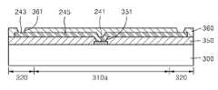
상기 제1반도체 칩(240)과 상기 제2반도체칩(250)은 듀얼 다이 패키지(DDP) 구조를 갖는다. 상기 제1패드들(243)은 상기 제1반도체 칩(240)의 양측 에지부에 재배선 공정을 통해 배열된다. 도 3a를 참조하면, 반도체 웨이퍼(300)의 제1칩 영역(310a)의 중앙부에 상기 제1칩 패드(241)가 배열되고, 상기 제1칩 패드(241)의 일부분을 노출시키는 제1개구부(351)를 구비하는 제1절연막(350)이 상기 웨이퍼(300)상에 형성된다. 상기 제1개구부(351)를 통해 상기 제1칩패드(241)에 전기적으로 연결되는 제1재배선 라인(245)이 상기 제1절연막(350)상에 상기 제1칩 영역(310a)으로부터 스크라이브 라인(320)까지 연장 형성된다. 상기 제1절연막(350)과 상기 제1재배선 라인(245)상에 제2절연막(360)을 형성한다. 상기 스크라이브 영역(320)의 제1재배선 라인(245)의 일부분은 상기 제2절연막(360)의 제3개구부(361)에 노출되어 제1패드(243)로 작용한다.The
상기 제2패드들(253)은 상기 제2반도체 칩(250)의 양측 에지부에 재배선 공 정을 통해 배열된다. 도 3b를 참조하면, 반도체 웨이퍼(300)의 제2칩 영역(310b)의 중앙부에 다수의 제2칩 패드(251)가 배열된다. 상기 웨이퍼(300)상에 상기 제2칩 패드(251)의 일부분을 노출시키는 제2개구부(353)를 구비하는 제1절연막(350)이 형성된다. 상기 제2개구부(353)를 통해 상기 제1칩 패드(251)에 전기적으로 연결되는 제2재배선 라인(255)이 상기 제2칩 영역(310b)의 상기 제1절연막(350)상에 형성된다. 상기 제1절연막(350)과 상기 제2재배선 라인(255)상에 제2절연막(360)을 형성한다. 제2재배선 라인(255)의 일부분은 상기 제2절연막(360)의 제4개구부(363)에 노출되어 제2패드(253)로 작용한다.The
도 4a 내지 도 6a는 도 2의 칩 스택 패키지의 제조방법을 설명하기 위한 평면도이다. 도 4b 내지 도 6b는 도 2의 칩 스택 패키지의 제조방법을 설명하기 위한 단면도이다. 도 4b 내지 도 6b는 각각 도 4a 내지 도 6a의 B-B 선에 따른 단면도이다.4A through 6A are plan views illustrating a method of manufacturing the chip stack package of FIG. 2. 4B to 6B are cross-sectional views illustrating a method of manufacturing the chip stack package of FIG. 2. 4B to 6B are cross-sectional views taken along line B-B of FIGS. 4A to 6A, respectively.
도 4a 및 도 4b를 참조하면, 반도체 웨이퍼(300)를 마련한다. 반도체 소자가 집적되는 다수의 칩 영역들(310a, 310b)과 상기 칩 영역들(310a, 310b)을 한정하는 스크라이브 영역(320)을 구비한다. 상기 제1반도체 칩들(240)이 집적될 상기 제1칩영역들(310a)과 상기 제2반도체 칩들(250)이 집적될 상기 제2칩 영역들(310b)은 교대로 배열된다. 상기 제1 및 제2칩 영역(310a, 310b)상에 반도체 소자(미도시)를 반도체 제조공정을 통해 집적하고, 상기 제1칩 영역(310a)의 중앙부에 나란하게 일렬로 배열되는 다수의 제1칩 패드들(241)과 제2칩 영역(310b)의 중앙부에 나란하게 일렬로 배열되는 다수의 제2칩 패드들(251)를 형성한다. 상기 제1칩 패드들(241)과 상기 제2칩 패드들(251)은 반도체 소자를 외부와 전기적으로 연결하는 패드로서, 예를 들어 알루미늄 패드를 포함할 수 있다.4A and 4B, a
도 5a 및 도 5b를 참조하면, 상기 제1칩 패드들(241)과 상기 제2칩 패드들(251)을 포함한 상기 웨이퍼(300)상에 제1절연막(350)을 형성한다. 상기 제1절연막(350)은 패시베이션막을 포함할 수 있다. 상기 제1절연막(350)은 SiO2, Si3N4, PSG(phospho silicate glass) 등을 포함할 수 있다. 상기 제1절연막(350)의 일부분을 식각하여, 상기 제1칩 패드들(241)을 노출시키는 제1개구부들(351)과 상기 제2칩 패드들(251)을 노출시키는 제2개구부들(353)을 각각 형성한다. 상기 제1절연막(350)상에 폴리머 계열의 절연물질을 포함하는 층간 절연막을 더 형성할 수 있다.5A and 5B, a first insulating
상기 제1절연막(350)상에 재배선 공정을 통해 제1재배선 라인들(245)와 제2재배선 라인들(255)을 형성한다. 상기 제1재배선 라인들(245)은 상기 제1칩 영역(310a)으로부터 상기 스크라이브 라인(320)까지 연장되도록 상기 제1절연막(350)상에 형성되어, 상기 제1개구부들(351)을 통해 상기 제1칩 패드들(241)에 연결되어진다. 상기 제2재배선 라인들(255)은 상기 제2칩 영역(310b)의 상기 제1절연막(350)상에 형성되어, 상기 제2개구부들(353)을 통해 상기 제2칩 패드들(251)에 연결되어진다. 상기 제1 및 제2재배선 라인들(245, 255)은 Cu와 같은 금속을 포함할 수 있다. 또한, 상기 제1 및 제2재배선 라인들(245, 255)은 Ti/Cu/Ni을 포함할 수도 있다.
상기 제1 및 제2재배선층들(245, 255)을 포함한 상기 제1절연막(350)상에 제 2절연막(360)을 형성한다. 상기 제2절연막(360)은 층간 절연막, 예를 들어 폴리머 계열의 절연막을 포함할 수 있다. 상기 제2절연막(360)은 상기 제1재배선 라인들(245)의 일부분들을 노출시켜 주는 제3개구부들(361)과 상기 제2재배선 라인들(255)의 일부분들을 노출시켜 주는 제4개구부들(363)을 구비한다. 상기 제3개구부들(361)은 상기 스크라이브 영역(320)에 배열된 상기 제1재배선 라인들(245)의 일부분들을 노출시켜 주도록 형성되고, 상기 제4개구부들(363)은 상기 제2칩 영역(310b)에 배열된 상기 제2재배선 라인들(255)의 일부분들을 노출시켜 주도록 형성된다. 상기 제3개구부들(361)에 의해 노출되는 제1재배선 라인들(245)의 일부분들은 제1패드들(243)으로 작용하고, 상기 제4개구부들(363)에 의해 노출되는 제2재배선 라인들(255)의 일부분들은 제2패드들(253)로 작용한다. 상기 제1패드들(243)은 상기 제1칩 영역(310a)을 벗어나 상기 스크라이브 라인(320)에 배열되고, 상기 제2패드들(253)은 상기 제2칩 영역(310b)에 배열된다.A second insulating
도 6a 및 도 6b를 참조하면, 상기 웨이퍼(300)를 상기 스크라이브 영역(320)내의 스크라이브 라인(340)을 따라 절단하여 제1반도체 칩(240)과 상기 제2반도체 칩(250)을 제조한다. 상기 제1반도체 칩(240)과 상기 제2반도체 칩(250)은 서로 다른 크기를 갖는다. 이어서, 다이 사이즈가 큰 상기 제1반도체 칩(240)을 제1접착제(230)를 통해 상기 기판(210)에 실장하고, 다이 사이즈가 작은 상기 제2반도체 칩(250)을 상기 제1반도체 칩(240)의 상기 제1칩 영역(310a)에 대응시켜 제2접착제(235)를 통해 실장한다. 이어서, 한번의 와이어 본딩공정을 수행하여, 상기 제1반도체 칩(240)의 상기 제1패드들(243)과 상기 기판(210)의 상기 제1회로 패턴 들(111)을 제1와이어(270)로 전기적으로 연결하고, 상기 제2반도체 칩(250)의 상기 제2패드들(253)과 상기 기판(210)의 상기 제1회로 패턴들(111)을 제2와이어(275)로 전기적으로 연결한다. 이어서, 몰딩공정을 수행하여 상기 제1 및 제2반도체 칩들(240, 250)과 상기 제1 및 제2와이어들(270, 275)을 봉지부(280)로 피복시켜 준다.6A and 6B, the
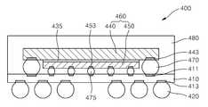
도 7은 본 발명의 다른 실시예에 따른 칩 스택 패키지의 단면도를 도시한 것이다. 도 7을 참조하면, 칩 스택 패키지(400)는 기판(410)과 상기 기판(410)상에 실장된 단위 반도체 칩(460)을 포함한다. 상기 단위 반도체 칩(460)은 다수의 반도체 칩, 예를 들어 제1반도체 칩(440)과 제2반도체 칩(450)이 적층된다. 상기 제1반도체 칩(440)과 상기 제2반도체 칩(450)의 활성면이 상기 기판(410)의 제1면과 마주보도록 적층된다. 이때, 다이 사이즈가 작은 제2반도체 칩(450)상에 다이 사이즈가 큰 제1반도체 칩(440)이 상기 접착제(435)를 통해 부착된다.7 illustrates a cross-sectional view of a chip stack package according to another embodiment of the present invention. Referring to FIG. 7, the
상기 제1반도체 칩(440)의 제1패드들(443)과 상기 기판(410)의 제1회로 패턴들(411)이 제1솔더 볼들(470)을 통해 전기적으로 연결되고, 상기 제2반도체 칩(450)의 제2패드들(453)과 상기 기판(410)의 상기 제1회로 패턴들(411)은 제2솔더 볼들(475)을 통해 전기적으로 연결된다. 상기 기판(410)의 제2면에 다수의 제2회로 패턴들(413)이 배열되고, 상기 제2회로 패턴들(413)에는 외부와의 접속을 위한 다수의 외부 접속단자들(420)이 각각 배열된다. 상기 제1 및 제2반도체 칩(440, 450)과 상기 제1 및 제2솔더 볼들(470, 475)은 봉지부(480)에 피복되어 보호된다.
칩 스택 패키지(400)은 도 4a 내지 도 6a 그리고 도 4b 내지 도 6b의 제조방법과 같은 방법으로 제조된다. 다만, 도 5a 및 도 5b의 재배선 공정후 상기 제1패드들(443)과 상기 제2패드들(453)의 상면에 상기 제1솔더 볼들(470)과 상기 제2솔더 볼들(475)을 각각 부착시켜 주는 공정이 더 추가될 수 있다. 상기 제1반도체 칩(440)과 상기 제2반도체 칩(450)으로 절단한 후, 상기 기판(410)의 상기 제1회로 패턴들(111)과 상기 제1반도체 칩(440)의 상기 제1솔더 볼들(470) 및 상기 제2반도체 칩(450)의 상기 제2솔더 볼들(475)은 와이어 본딩공정없이 페이스-투-페이스 본딩된다.The
도 8은 본 발명의 또 다른 실시예에 따른 칩 스택 패키지의 단면도이다. 도 7을 참조하면, 칩 스택 패키지(500)는 단위 반도체 칩(560)으로 다수의 반도체 칩, 예를 들어 4개의 반도체 칩(540, 545, 550, 555)이 적층된 구조를 갖는다. 상기 제1 내지 제4반도체 칩들(540, 545, 550, 555)이 제1 내지 제4접착제들(530, 533, 535, 537)을 통해 상기 기판(510)상에 실장되고, 상기 제1 내지 제4반도체 칩들(540, 545, 550, 555)의 제1 내지 제4패드들(543, 547, 553, 557)은 제1 내지 제4와이어들(570, 573, 575, 577)을 통해 상기 기판(510)의 제1면에 배열된 제1회로 패턴들(511)과 전기적으로 연결된다. 상기 기판(510)은 제2면에 배열된 제2회로 패턴들(513)과 상기 제2회로 패턴들(513)에 부착된 외부 접속단자들(520)을 더 포함한다. 상기 제1 내지 제4반도체 칩들(540, 545, 550, 555)과 상기 제1 내지 제4와이어들(570, 573, 575, 577)은 봉지부(580)에 의해 피복되어 보호된다.8 is a cross-sectional view of a chip stack package according to another embodiment of the present invention. Referring to FIG. 7, the
상기 칩 스택 패키지(500)는 도 4a 내지 도 6a 및 도 4b 내지 도 6b에 도시 된 제조방법과 동일한 방법으로 제조된다. 다만, 최상층에 배열되는 제4반도체 칩(555)의 상기 제4패드들(557)은 제4칩영역(도 4a의 310b 에 대응함)에 배열되고, 상기 제1 내지 제3반도체 칩(540, 545, 550)의 상기 제1 내지 제3패드들(543, 547, 553)은 제1 내지 제3칩영역(도 4a의 310a 대응함)을 벗어나 스크라이브 영역(도 4a의 320에 대응함)에 배열되도록 단위 반도체 칩(560)을 제조한다. 이때, 상기 제1내지 제3반도체 칩(540, 545, 550)의 크기가 서로 상이하므로, 상기 제1 내지 제3패드들(543, 547, 553)이 순차적으로 상기 제1칩 영역(310a)으로부터 멀어지도록 상기 스크라이브 라인(320)에 배열한다.The
이상에서 자세히 설명한 바와 같이, 본 발명의 칩 스택 패키지 및 그 제조방법에 따르면, 추가 공정없이 스크라이브 영역에 패드를 재배치하여 서로 다른 크기를 갖는 반도체 칩을 순차적으로 적층시켜 줌으로써 와이어 루프에 무관하게 와이어 본딩이 가능하게 할 수 있으며, 이에 따라 패키지 두께를 감소시켜 줄 수 있다. 또한, 한번의 와이어 본딩공정을 통해 반도체 칩과 기판을 전기적으로 연결시켜 줄 수 있으므로, 공정을 단순화할 수 있다.As described in detail above, according to the chip stack package of the present invention and a method of manufacturing the same, wire bonding is performed regardless of the wire loop by sequentially stacking semiconductor chips having different sizes by repositioning pads in a scribe area without an additional process. This can be enabled, thereby reducing the package thickness. In addition, since the semiconductor chip and the substrate may be electrically connected through a single wire bonding process, the process may be simplified.
이상 본 발명을 바람직한 실시예를 들어 상세하게 설명하였으나, 본 발명은 상기 실시예에 한정되지 않고, 본 발명의 기술적 사상의 범위 내에서 당 분야에서 통상의 지식을 가진 자에 의하여 여러가지 변형이 가능하다.Although the present invention has been described in detail with reference to preferred embodiments, the present invention is not limited to the above embodiments, and various modifications may be made by those skilled in the art within the scope of the technical idea of the present invention. .
Claims (20)
Translated fromKoreanPriority Applications (2)
| Application Number | Priority Date | Filing Date | Title |
|---|---|---|---|
| KR1020070035176AKR100871709B1 (en) | 2007-04-10 | 2007-04-10 | Chip stack package and manufacturing method thereof |
| US12/100,359US7948089B2 (en) | 2007-04-10 | 2008-04-09 | Chip stack package and method of fabricating the same |
Applications Claiming Priority (1)
| Application Number | Priority Date | Filing Date | Title |
|---|---|---|---|
| KR1020070035176AKR100871709B1 (en) | 2007-04-10 | 2007-04-10 | Chip stack package and manufacturing method thereof |
Publications (2)
| Publication Number | Publication Date |
|---|---|
| KR20080091980A KR20080091980A (en) | 2008-10-15 |
| KR100871709B1true KR100871709B1 (en) | 2008-12-08 |
Family
ID=39852973
Family Applications (1)
| Application Number | Title | Priority Date | Filing Date |
|---|---|---|---|
| KR1020070035176AActiveKR100871709B1 (en) | 2007-04-10 | 2007-04-10 | Chip stack package and manufacturing method thereof |
Country Status (2)
| Country | Link |
|---|---|
| US (1) | US7948089B2 (en) |
| KR (1) | KR100871709B1 (en) |
Families Citing this family (18)
| Publication number | Priority date | Publication date | Assignee | Title |
|---|---|---|---|---|
| WO2009035849A2 (en) | 2007-09-10 | 2009-03-19 | Vertical Circuits, Inc. | Semiconductor die mount by conformal die coating |
| CN101999167B (en) | 2008-03-12 | 2013-07-17 | 伊文萨思公司 | Support mounted electrically interconnected die assembly |
| US9153517B2 (en) | 2008-05-20 | 2015-10-06 | Invensas Corporation | Electrical connector between die pad and z-interconnect for stacked die assemblies |
| US8743561B2 (en) | 2009-08-26 | 2014-06-03 | Taiwan Semiconductor Manufacturing Company, Ltd. | Wafer-level molded structure for package assembly |
| WO2011056668A2 (en) | 2009-10-27 | 2011-05-12 | Vertical Circuits, Inc. | Selective die electrical insulation additive process |
| KR101695846B1 (en)* | 2010-03-02 | 2017-01-16 | 삼성전자 주식회사 | Stacked semiconductor packages |
| KR101185860B1 (en)* | 2010-12-17 | 2012-09-25 | 에스케이하이닉스 주식회사 | Semiconductor chip and semiconductor package having the same |
| KR102387541B1 (en)* | 2015-03-25 | 2022-04-18 | 삼성전자주식회사 | Semiconductor chip, and flip chip package and wafer level package including the same |
| KR101691099B1 (en)* | 2015-04-30 | 2016-12-29 | 하나 마이크론(주) | Fan-out package, Package-On-Package and manufacturing method thereof |
| US9871019B2 (en) | 2015-07-17 | 2018-01-16 | Invensas Corporation | Flipped die stack assemblies with leadframe interconnects |
| US9490195B1 (en) | 2015-07-17 | 2016-11-08 | Invensas Corporation | Wafer-level flipped die stacks with leadframes or metal foil interconnects |
| US9825002B2 (en) | 2015-07-17 | 2017-11-21 | Invensas Corporation | Flipped die stack |
| US9508691B1 (en) | 2015-12-16 | 2016-11-29 | Invensas Corporation | Flipped die stacks with multiple rows of leadframe interconnects |
| US10566310B2 (en) | 2016-04-11 | 2020-02-18 | Invensas Corporation | Microelectronic packages having stacked die and wire bond interconnects |
| US9595511B1 (en) | 2016-05-12 | 2017-03-14 | Invensas Corporation | Microelectronic packages and assemblies with improved flyby signaling operation |
| KR102538175B1 (en) | 2016-06-20 | 2023-06-01 | 삼성전자주식회사 | Semiconductor package |
| US10204884B2 (en)* | 2016-06-29 | 2019-02-12 | Intel Corporation | Multichip packaging for dice of different sizes |
| US9728524B1 (en) | 2016-06-30 | 2017-08-08 | Invensas Corporation | Enhanced density assembly having microelectronic packages mounted at substantial angle to board |
Citations (1)
| Publication number | Priority date | Publication date | Assignee | Title |
|---|---|---|---|---|
| KR20020047746A (en)* | 2000-12-14 | 2002-06-22 | 마이클 디. 오브라이언 | wire bonding method and semiconductor package using it |
Family Cites Families (5)
| Publication number | Priority date | Publication date | Assignee | Title |
|---|---|---|---|---|
| US6250192B1 (en)* | 1996-11-12 | 2001-06-26 | Micron Technology, Inc. | Method for sawing wafers employing multiple indexing techniques for multiple die dimensions |
| JP3916854B2 (en)* | 2000-06-28 | 2007-05-23 | シャープ株式会社 | Wiring board, semiconductor device, and package stack semiconductor device |
| JP2003163327A (en) | 2001-11-29 | 2003-06-06 | Sony Corp | Semiconductor chip, semiconductor wafer and dicing method thereof, and stacked semiconductor device |
| KR100537892B1 (en) | 2003-08-26 | 2005-12-21 | 삼성전자주식회사 | Chip stack package and manufacturing method thereof |
| US7326592B2 (en)* | 2005-04-04 | 2008-02-05 | Infineon Technologies Ag | Stacked die package |
- 2007
- 2007-04-10KRKR1020070035176Apatent/KR100871709B1/enactiveActive
- 2008
- 2008-04-09USUS12/100,359patent/US7948089B2/enactiveActive
Patent Citations (1)
| Publication number | Priority date | Publication date | Assignee | Title |
|---|---|---|---|---|
| KR20020047746A (en)* | 2000-12-14 | 2002-06-22 | 마이클 디. 오브라이언 | wire bonding method and semiconductor package using it |
Also Published As
| Publication number | Publication date |
|---|---|
| KR20080091980A (en) | 2008-10-15 |
| US7948089B2 (en) | 2011-05-24 |
| US20080251939A1 (en) | 2008-10-16 |
Similar Documents
| Publication | Publication Date | Title |
|---|---|---|
| KR100871709B1 (en) | Chip stack package and manufacturing method thereof | |
| US10734367B2 (en) | Semiconductor package and method of fabricating the same | |
| US6818998B2 (en) | Stacked chip package having upper chip provided with trenches and method of manufacturing the same | |
| US10032705B2 (en) | Semiconductor package and manufacturing method thereof | |
| KR101494413B1 (en) | Support frame, and method of manufacturing semiconductor package using the same | |
| JP2009044110A (en) | Semiconductor device and its manufacturing method | |
| KR102736227B1 (en) | Circuit board and semiconductor package | |
| KR101964389B1 (en) | Integrated circuit packaging system with vertical interconnects and method of manufacture thereof | |
| US11961775B2 (en) | Semiconductor devices and related methods | |
| TWI654727B (en) | Chip packaging method | |
| CN107403785B (en) | Electronic package and manufacturing method thereof | |
| TWI594382B (en) | Electronic package and method of manufacture | |
| US20220352059A1 (en) | Semiconductor package and manufacturing method thereof | |
| KR100890073B1 (en) | Vertically Stacked Semiconductor Devices and Manufacturing Method Thereof | |
| US9299650B1 (en) | Integrated circuit packaging system with single metal layer interposer and method of manufacture thereof | |
| KR20140115597A (en) | Semiconductor package, semiconductor package unit, and method of manufacturing semiconductor package | |
| KR20200139088A (en) | Semiconductor devices and related methods | |
| CN113257775A (en) | Semiconductor device package and method of manufacturing the same | |
| KR101345035B1 (en) | Semiconductor package and fabricating method thereof | |
| TW202029448A (en) | Electronic package and package substrate thereof and method for manufacturing same | |
| KR20040102414A (en) | semiconductor package | |
| TWI897644B (en) | Semiconductor devices and related methods | |
| TWI818719B (en) | Carrier structure | |
| KR20010073946A (en) | Semiconductor device and manufacturing method of the same with dimple type side pad | |
| WO2014103855A1 (en) | Semiconductor device and manufacturing method therefor |
Legal Events
| Date | Code | Title | Description |
|---|---|---|---|
| A201 | Request for examination | ||
| PA0109 | Patent application | Patent event code:PA01091R01D Comment text:Patent Application Patent event date:20070410 | |
| PA0201 | Request for examination | ||
| E902 | Notification of reason for refusal | ||
| PE0902 | Notice of grounds for rejection | Comment text:Notification of reason for refusal Patent event date:20080325 Patent event code:PE09021S01D | |
| E701 | Decision to grant or registration of patent right | ||
| PE0701 | Decision of registration | Patent event code:PE07011S01D Comment text:Decision to Grant Registration Patent event date:20080930 | |
| PG1501 | Laying open of application | ||
| GRNT | Written decision to grant | ||
| PR0701 | Registration of establishment | Comment text:Registration of Establishment Patent event date:20081126 Patent event code:PR07011E01D | |
| PR1002 | Payment of registration fee | Payment date:20081127 End annual number:3 Start annual number:1 | |
| PG1601 | Publication of registration | ||
| PR1001 | Payment of annual fee | Payment date:20111101 Start annual number:4 End annual number:4 | |
| FPAY | Annual fee payment | Payment date:20121031 Year of fee payment:5 | |
| PR1001 | Payment of annual fee | Payment date:20121031 Start annual number:5 End annual number:5 | |
| FPAY | Annual fee payment | Payment date:20131031 Year of fee payment:6 | |
| PR1001 | Payment of annual fee | Payment date:20131031 Start annual number:6 End annual number:6 | |
| FPAY | Annual fee payment | Payment date:20141031 Year of fee payment:7 | |
| PR1001 | Payment of annual fee | Payment date:20141031 Start annual number:7 End annual number:7 | |
| FPAY | Annual fee payment | Payment date:20151030 Year of fee payment:8 | |
| PR1001 | Payment of annual fee | Payment date:20151030 Start annual number:8 End annual number:8 | |
| FPAY | Annual fee payment | Payment date:20181031 Year of fee payment:11 | |
| PR1001 | Payment of annual fee | Payment date:20181031 Start annual number:11 End annual number:11 | |
| FPAY | Annual fee payment | Payment date:20191031 Year of fee payment:12 | |
| PR1001 | Payment of annual fee | Payment date:20191031 Start annual number:12 End annual number:12 | |
| PR1001 | Payment of annual fee | Payment date:20201030 Start annual number:13 End annual number:13 | |
| PR1001 | Payment of annual fee | Payment date:20211027 Start annual number:14 End annual number:14 | |
| PR1001 | Payment of annual fee | Payment date:20221026 Start annual number:15 End annual number:15 | |
| PR1001 | Payment of annual fee | Payment date:20231026 Start annual number:16 End annual number:16 | |
| PR1001 | Payment of annual fee | Payment date:20241024 Start annual number:17 End annual number:17 |