KR100871016B1 - Illumination apparatus, exposure apparatus having the same, and device manufacturing method - Google Patents
Illumination apparatus, exposure apparatus having the same, and device manufacturing methodDownload PDFInfo
- Publication number
- KR100871016B1 KR100871016B1KR1020070029097AKR20070029097AKR100871016B1KR 100871016 B1KR100871016 B1KR 100871016B1KR 1020070029097 AKR1020070029097 AKR 1020070029097AKR 20070029097 AKR20070029097 AKR 20070029097AKR 100871016 B1KR100871016 B1KR 100871016B1
- Authority
- KR
- South Korea
- Prior art keywords
- light
- polarization
- phase plate
- optical system
- phase
- Prior art date
- Legal status (The legal status is an assumption and is not a legal conclusion. Google has not performed a legal analysis and makes no representation as to the accuracy of the status listed.)
- Expired - Fee Related
Links
Images


Classifications
- G—PHYSICS
- G03—PHOTOGRAPHY; CINEMATOGRAPHY; ANALOGOUS TECHNIQUES USING WAVES OTHER THAN OPTICAL WAVES; ELECTROGRAPHY; HOLOGRAPHY
- G03B—APPARATUS OR ARRANGEMENTS FOR TAKING PHOTOGRAPHS OR FOR PROJECTING OR VIEWING THEM; APPARATUS OR ARRANGEMENTS EMPLOYING ANALOGOUS TECHNIQUES USING WAVES OTHER THAN OPTICAL WAVES; ACCESSORIES THEREFOR
- G03B27/00—Photographic printing apparatus
- G03B27/32—Projection printing apparatus, e.g. enlarger, copying camera
- G03B27/52—Details
- G03B27/54—Lamp housings; Illuminating means
- G—PHYSICS
- G03—PHOTOGRAPHY; CINEMATOGRAPHY; ANALOGOUS TECHNIQUES USING WAVES OTHER THAN OPTICAL WAVES; ELECTROGRAPHY; HOLOGRAPHY
- G03F—PHOTOMECHANICAL PRODUCTION OF TEXTURED OR PATTERNED SURFACES, e.g. FOR PRINTING, FOR PROCESSING OF SEMICONDUCTOR DEVICES; MATERIALS THEREFOR; ORIGINALS THEREFOR; APPARATUS SPECIALLY ADAPTED THEREFOR
- G03F7/00—Photomechanical, e.g. photolithographic, production of textured or patterned surfaces, e.g. printing surfaces; Materials therefor, e.g. comprising photoresists; Apparatus specially adapted therefor
- G03F7/70—Microphotolithographic exposure; Apparatus therefor
- G03F7/70058—Mask illumination systems
- G03F7/70191—Optical correction elements, filters or phase plates for controlling intensity, wavelength, polarisation, phase or the like
- G—PHYSICS
- G03—PHOTOGRAPHY; CINEMATOGRAPHY; ANALOGOUS TECHNIQUES USING WAVES OTHER THAN OPTICAL WAVES; ELECTROGRAPHY; HOLOGRAPHY
- G03F—PHOTOMECHANICAL PRODUCTION OF TEXTURED OR PATTERNED SURFACES, e.g. FOR PRINTING, FOR PROCESSING OF SEMICONDUCTOR DEVICES; MATERIALS THEREFOR; ORIGINALS THEREFOR; APPARATUS SPECIALLY ADAPTED THEREFOR
- G03F7/00—Photomechanical, e.g. photolithographic, production of textured or patterned surfaces, e.g. printing surfaces; Materials therefor, e.g. comprising photoresists; Apparatus specially adapted therefor
- G03F7/70—Microphotolithographic exposure; Apparatus therefor
- G03F7/70483—Information management; Active and passive control; Testing; Wafer monitoring, e.g. pattern monitoring
- G03F7/7055—Exposure light control in all parts of the microlithographic apparatus, e.g. pulse length control or light interruption
- G03F7/70566—Polarisation control
Landscapes
- Physics & Mathematics (AREA)
- General Physics & Mathematics (AREA)
- Exposure And Positioning Against Photoresist Photosensitive Materials (AREA)
- Exposure Of Semiconductors, Excluding Electron Or Ion Beam Exposure (AREA)
Abstract
Translated fromKorean

Description
Translated fromKorean도 1은 본 발명의 일 측면에 의한 노광장치의 구성을 나타낸 개략 단면도;1 is a schematic cross-sectional view showing the configuration of an exposure apparatus according to an aspect of the present invention;
도 2는 도 1에 나타낸 노광장치의 편향계의 하나의 예시적인 구성을 나타낸 개략 단면도;FIG. 2 is a schematic cross-sectional view showing one exemplary configuration of the deflectometer of the exposure apparatus shown in FIG. 1; FIG.
도 3A 및 도 3B는 도 1에 나타낸 조명 광학계에 있어서의 위상판의 개략 단면도 및 개략 정면도;3A and 3B are schematic sectional views and a schematic front view of a phase plate in the illumination optical system shown in FIG. 1;
도 4A 내지 도 4C는 x-편광이 입사했을 경우에, 위상판의 진상축 방향(위치)과 사출되는 광의 편광 상태와의 관계를 나타낸 도면;4A to 4C are diagrams showing the relationship between the fast axis direction (position) of the phase plate and the polarization state of the emitted light when x-polarized light is incident;
도 5는 위상판의 두께와 편광도와의 관계를 설명하기 위한 도면;5 is a diagram for explaining a relationship between a thickness of a phase plate and a polarization degree;
도 6은 도 5에 나타낸 위상판의 두께와 편광도와의 관계를 나타낸 도면;FIG. 6 is a view showing a relationship between a thickness and a polarization degree of the phase plate shown in FIG. 5; FIG.
도 7은 도 1에 나타낸 노광장치에 이용할 수 있는 위상판의 두께와 입사각과의 관계를 나타낸 그래프;FIG. 7 is a graph showing the relationship between the thickness and the incident angle of the phase plate which can be used in the exposure apparatus shown in FIG. 1; FIG.
도 8은 위상판의 유리재로서 사파이어를 사용했을 경우에, 도 1에 나타낸 노광장치에 이용할 수 있는 위상판의 두께와 입사각과의 관계를 나타낸 그래프;8 is a graph showing the relationship between the thickness of the phase plate and the incident angle which can be used in the exposure apparatus shown in FIG. 1 when sapphire is used as the glass material of the phase plate;
도 9는 도 1에 나타낸 노광장치의 광정형화 유닛의 구성의 일례를 나타낸 개 략 단면도;9 is a schematic cross-sectional view showing an example of the configuration of a light shaping unit of the exposure apparatus shown in FIG. 1;
도 10A 및 도 10B는 도 1에 나타낸 노광장치의 위상판의 하나의 예시적인 구성을 나타낸 개략 정면도;10A and 10B are schematic front views showing one exemplary configuration of a phase plate of the exposure apparatus shown in FIG. 1;
도 11A 및 도 11B는 도 1에 나타낸 노광장치의 위상판의 하나의 예시적인 구성을 나타낸 개략 정면도;11A and 11B are schematic front views showing one exemplary configuration of the phase plate of the exposure apparatus shown in FIG. 1;
도 12A 내지 도 12C는 도 1에 나타낸 노광장치에 있어서, 유효 광원 형성 유닛보다 후단의 유리재의 복굴절을 변화시켰을 때의 콘트라스트, 좌우 선폭("CD": Critical Dimention)차, 축상축외(axial-off-axial) CD차 등의 각종 특성의 변화를 나타낸 그래프;12A to 12C show contrast, left and right line width ("CD") differences, and axial-off when the birefringence of the glass material at the rear end of the effective light source forming unit is changed in the exposure apparatus shown in FIG. -axial) a graph showing changes in various characteristics such as a CD difference;
도 13은 형석의 진성 복굴절을 설명하기 위한 도면;13 is a view for explaining the intrinsic birefringence of fluorspar;
도 14A 및 도 14B는 형석의 회전 방향을 최적화하고 있지 않은 경우의 진성 복굴절에 의한 편광 시프트를 설명하기 위한 도면;14A and 14B are views for explaining polarization shift due to intrinsic birefringence when the rotation direction of fluorite is not optimized;
도 15A 및 도 15B는 형석의 회전 방향을 최적화하고 있는 경우의 진성 복굴절에 의한 편광 시프트를 설명하기 위한 도면;15A and 15B are views for explaining polarization shift due to intrinsic birefringence when the rotational direction of fluorite is optimized;
도 16A 및 도 16B는 형석에 경사각 오차가 발생했을 경우의 경사각 오차와 편광 시프트량과의 상관을 설명하기 위한 도면;16A and 16B are diagrams for explaining the correlation between the tilt angle error and the amount of polarization shift when the tilt angle error occurs in the fluorite;
도 17A 및 도 17B는 형석에 회전각 오차가 발생했을 경우의 회전각 오차와 편광 시프트량과의 상관을 설명하기 위한 도면;17A and 17B are diagrams for explaining a correlation between a rotation angle error and a polarization shift amount when a rotation angle error occurs in fluorite;
도 18A 및 도 18B는 협대역 고반사(NBHR) 코팅 또는 광대역 고반사(BBHR) 코팅의 입사각과 위상차와의 관계를 나타낸 그래프;18A and 18B are graphs showing the relationship between the angle of incidence and phase difference of a narrow band high reflection (NBHR) coating or a wide band high reflection (BBHR) coating;
도 19A 및 도 19B는 협대역 고반사(NBHR) 코팅 또는 광대역 고반사(BBHR) 코팅의 각 편광 방향에 대한 편광 붕괴를 나타낸 도면;19A and 19B show polarization decay for each polarization direction of a narrowband high reflection (NBHR) coating or a broadband high reflection (BBHR) coating;
도 20은 투과막의 입사각과 위상차와의 관계를 나타낸 그래프;20 is a graph showing a relationship between an incident angle and a phase difference of a permeable membrane;
도 21은 투과막의 각 편광 방향(x-편광, y-편광, 45°편광 및 -45°편광에 대한 동공 내의 편광 시프트를, 웨이퍼 면 위의 상점(0, 0), (13, 0) 및 (13, 4.5)에서 추정한 결과를 나타낸 도면;FIG. 21 shows the polarization shift in the pupil for each polarization direction (x-polarized, y-polarized, 45 ° polarized and -45 ° polarized) of the transmissive membrane, store (0, 0), (13, 0) on the wafer surface and Fig. 13 shows the result of estimation in (13, 4.5);
도 22는 편광도 및 편광 시프트량의 정의를 설명하기 위한 도면;22 is a diagram for explaining definition of polarization degree and polarization shift amount;
도 23은 디바이스의 제조를 설명하기 위한 순서도;23 is a flow chart for explaining the manufacture of the device;
도 24는 도 23에 나타낸 스텝 4의 상세한 순서도.24 is a detailed flowchart of
<도면의 주요부분에 대한 부호의 설명><Description of the symbols for the main parts of the drawings>
1: 노광장치10: 조명장치1: exposure apparatus 10: lighting apparatus
12: 광원20: 레티클12: light source 20: reticle
30: 투영 광학계40: 웨이퍼30: projection optical system 40: wafer
45: 웨이퍼 스테이지60: 제어기45: wafer stage 60: controller
70, 80: 검출기100: 조명 광학계70, 80: detector 100: illumination optical system
114, 122, 159: 위상판124: 편광 해소판114, 122, 159: Phase plate 124: Polarization canceling plate
155: σ형상 보정 기구155: σ shape correction mechanism
본 발명은 조명 광학계 및 노광장치에 관한 것이다.The present invention relates to an illumination optical system and an exposure apparatus.
포토리소그래피 기술을 이용해서 반도체소자를 제조할 때에, 레티클의 회로 패턴을 투영 광학계를 통해서 웨이퍼 등에 투영해서 회로 패턴을 전사하는 투영 노광장치가 종래부터 사용되고 있다.When manufacturing a semiconductor device using photolithography technology, the projection exposure apparatus which transfers a circuit pattern by projecting the circuit pattern of a reticle through a projection optical system etc. is conventionally used.
근래에는 반도체소자의 미세화 요구에 수반해서, 노광 파장의 절반 이하의 크기의 패턴을 노광하는 또는 고해상을 달성하는 노광장치도 개발되어 있다. 고해상도는 일반적으로 단파장 및/또는 높은 개구수(NA)를 지닌 투영 광학계를 이용함으로써 달성된다. 투영 광학계의 고NA화는 상면의 수선과 입사광의 진행 방향이 이루는 각이 커지는 것을 의미하고 있어, 고 NA 결상으로 불린다.In recent years, with the demand for miniaturization of semiconductor devices, exposure apparatuses for exposing a pattern having a size smaller than half of an exposure wavelength or achieving high resolution have also been developed. High resolution is generally achieved by using projection optics with short wavelengths and / or high numerical aperture (NA). Higher NA of the projection optical system means that the angle formed by the repair line on the image plane and the traveling direction of the incident light becomes larger, which is called high NA imaging.
그러나, 고 NA 결상으로 노광했을 경우, 노광광의 편광이 문제가 된다. 예를 들면, 라인과 스페이스가 반복되고 있는 소위 라인-앤드-스페이스("L&S") 패턴을 노광하는 경우를 고려한다. L&S 패턴은 평면파 2 광속 간섭에 의해서 노광된다. 2 광속의 입사 방향 벡터를 포함하는 면을 입사 평면으로 하고, 이 입사 평면에 수직인 편광을 s-편광, 입사 평면에 평행한 편광을 p-편광으로 한다. 2 광속의 입사 방향 벡터가 서로 이루는 각이 90°인 경우, s-편광은 간섭하므로 L&S 패턴에 따른 광강도 분포가 상 면 위에 형성된다. 한편, p-편광은 간섭하지 않으므로(간섭의 효과가 소거되므로) 광강도 분포는 일정하게 되어, L&S 패턴에 따른 광강도 분포가 상 면 위에 형성되는 일은 없다. s-편광과 p-편광이 혼재하고 있으면, s-편광뿐일 때보다 콘트라스트가 나쁜 광강도 분포가 상 면 위에 형성되고, p-편광의 비율이 커지면 상 면 위의 광강도 분포의 콘트라스트가 저하하여, 최종적 으로는 패턴이 형성되지 않게 된다.However, when exposing with high NA imaging, polarization of exposure light becomes a problem. For example, consider the case of exposing a so-called line-and-space ("L & S") pattern in which lines and spaces are repeated. The L & S pattern is exposed by plane wave two light beam interference. The plane containing the incidence direction vector of two light beams is made into the incidence plane, s-polarized light is perpendicular to the incidence plane and p-polarized light is parallel to the incidence plane. When the angle between the incidence vectors of the two light beams is 90 °, the s-polarized light interferes, and thus the light intensity distribution according to the L & S pattern is formed on the image plane. On the other hand, since p-polarized light does not interfere (the effect of interference is canceled), the light intensity distribution becomes constant, and the light intensity distribution according to the L & S pattern is not formed on the upper surface. When s-polarized light and p-polarized light are mixed, a light intensity distribution having a lower contrast than that of s-polarized light is formed on the upper surface, and as the ratio of p-polarized light increases, the contrast of the light intensity distribution on the upper surface is lowered. As a result, a pattern is not finally formed.
이 때문에, 노광광의 편광을 제어할 필요가 있어, 기초 실험 등도 행해지고 있다. 또한, 노광광의 편광 제어는 일반적으로는 조명 광학계의 동공면 및/또는 투영 광학계의 동공면에서 행해진다. 조명 광학계의 동공면에서 편광 제어된 노광광은 조명 광학계의 동공면 이후의 광학계를 개입시켜 레티클을 조명하고, 더욱, 투영 광학계에 의해서 집광되어 상 면 위에 결상된다. 편광 제어된 노광광은 충분한 콘트라스트의 광강도 분포를 상 면 위에 형성할 수 있어 보다 미세한 패턴을 노광하는 것이 가능해진다. 예를 들면, 광원으로부터의 광의 편광 상태를 바람직한 편광 상태로 제어하는 위상판을 지녀, 바람직한 편광 상태의 광으로 레티클을 조명함으로써 고해상을 달성하는 노광장치가 제안되어 있다(국제 공개 제 2004/051717호 공보 참조).For this reason, it is necessary to control the polarization of exposure light, and the basic experiment etc. are also performed. In addition, polarization control of exposure light is generally performed in the pupil plane of an illumination optical system, and / or the pupil plane of a projection optical system. The exposure light polarized in the pupil plane of the illumination optical system illuminates the reticle through the optical system after the pupil plane of the illumination optical system, and is further condensed by the projection optical system and formed on the image plane. The polarization-controlled exposure light can form a light intensity distribution of sufficient contrast on the image surface, thereby making it possible to expose a finer pattern. For example, an exposure apparatus has been proposed which has a phase plate for controlling the polarization state of light from a light source to a desired polarization state and achieves high resolution by illuminating the reticle with light of a preferred polarization state (International Publication 2004/051717). Publication).
그렇지만, 조명 광학계나 투영 광학계 등의 실제의 노광 광학계는 이상적인 편광 상태를 악화시키는 여러 요인을 지닌다. 이들 요인은 광원으로부터의 광의 편광 상태의 악화, 노광 광학계에 이용되는 석영이나 형석 등의 유리재가 가진 진성 복굴절("IBR"), 기계적 억제에 의해서 발생하는 응력 복굴절 및 반사 방지막이나 반사막 등의 광학막의 위상 특성을 포함한다. 또, 고 NA화가 진행됨에 따라서, 각도 분포를 가지는 광에 대한 위상판의 위상 오차도 상기 요인의 큰 비중을 차지하고 있다. 이들 요인에 의해서, 광원으로부터의 광이 이상적인 것에 가까운 직선 편광이어도, 웨이퍼면 위에서는 각 광선의 편광 상태가 시프트되게 된다.However, actual exposure optical systems such as illumination optical systems and projection optical systems have various factors that deteriorate the ideal polarization state. These factors include deterioration of the polarization state of light from a light source, intrinsic birefringence ("IBR") of glass materials such as quartz and fluorite used in the exposure optical system, stress birefringence caused by mechanical inhibition, and optical films such as antireflection films and reflective films. Includes phase characteristics. In addition, as the high NA progresses, the phase error of the phase plate with respect to the light having an angular distribution also occupies a large proportion of the above factors. By these factors, even if the light from the light source is linearly polarized light close to the ideal, the polarization state of each light beam is shifted on the wafer surface.
그래서, 웨이퍼 면 위에 있어서 바람직한 편광 상태를 얻기 위해서는 상술한 요인을 가능한 한 낮게 유지할 필요가 있다. 그렇지만, 상기 공보에는 위상판의 위상 오차에 대한 구체적인 대책이 제안되어 있지 않다. 즉, 상기 공보에서는 편광을 제어하는 위상판의 두께가 두꺼운 경우, 각도 분포를 가지는 광을 바람직한 편광 상태로 제어할 수 없다.Therefore, in order to obtain a desirable polarization state on the wafer surface, it is necessary to keep the above factors as low as possible. However, the above publication does not propose specific measures for the phase error of the phase plate. That is, in the above publication, when the thickness of the phase plate for controlling polarization is thick, the light having the angular distribution cannot be controlled in the preferred polarization state.
본 발명은 피조명면에 있어서의 편광 상태를 바람직한 상태로 유지할 수 있고, 각도 분포를 가지는 광의 편광 상태를 정밀하게 제어할 수 있는 조명 광학계에 관한 것이다.This invention relates to the illumination optical system which can maintain the polarization state in a to-be-illuminated surface to a preferable state, and can precisely control the polarization state of the light which has an angle distribution.
광원으로부터의 광을 이용해서 피조명면을 조명하는 조명 광학계는 상기 광의 편광 상태를 변경하는 편광 변환부를 구비하고, 상기 편광 변환부는 제 1 위상판과 제 2 위상판을 포함하되, 상기 제 1 위상판은 상기 편광 변환부에 입사하는 광속의 입사각 θ를 이용해서 하기 식을 만족하도록 결정된 두께 d를 가지고, 상기 제 2 위상판은 상기 제 1 위상판 또는 제 2 위상판을 통과하는 광의, 서로 수직인 주축 방향으로 진동하는 직선편광성분 간에 소정의 위상차가 얻어지도록 결정된 두께의 차이 분만큼 상기 제 1위상판의 두께와는 다른 두께를 가지는 것을 특징으로 한다:An illumination optical system for illuminating an illuminated surface using light from a light source includes a polarization converting portion for changing a polarization state of the light, and the polarization converting portion includes a first phase plate and a second phase plate, wherein the first phase The plate has a thickness d determined to satisfy the following equation using the incident angle θ of the light beam incident on the polarization converting portion, and the second phase plate is perpendicular to each other of the light passing through the first phase plate or the second phase plate. It is characterized by having a thickness different from the thickness of the first phase plate by the difference in the thickness determined so as to obtain a predetermined phase difference between the linearly polarized light components oscillating in the principal axis direction:

(식 중, λ는 상기 광의 파장이고, Δn은 제 1 위상판의 복굴절률임).(Wherein λ is the wavelength of the light and Δn is the birefringence of the first phase plate).
본 발명의 또 다른 목적 또는 그 외의 특징은 첨부 도면을 참조해서 이하에 설명되는 바람직한 실시예에 의해 명백해질 것이다.Further objects or other features of the present invention will become apparent from the preferred embodiments described below with reference to the accompanying drawings.
이하에, 본 발명의 실시형태를 첨부 도면에 따라 상세히 설명할 것이다.EMBODIMENT OF THE INVENTION Below, embodiment of this invention is described in detail according to an accompanying drawing.
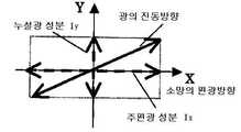
우선, 본 출원에서는 편광 조명의 성능의 지표로서 편광도의 양을 정의한다. 도 22는 편광도 및 편광 시프트량(polarization shift amount)의 정의를 설명하기 위한 도면이다. 도 22는 바람직한 편광 방향인 X축 방향으로부터 시프트된 전장 벡터 진동면을 가진 광을 나타내고 있다. 도 22에 있어서, 바람직한 편광 방향인 X축 방향으로 진동하는 전장 벡터를 가진 (주편광)광의 성분의 강도를 Ix, 바람직한 편광 방향인 X축 방향에 대해서 직교하는 Y축 방향으로 진동하는 전장 벡터를 가진 (누설)광의 성분의 강도를 Iy라 한다. 이 경우, 편광도를 Ix/(Ix+Iy)라고 정의한다. 또, 편광도가 시프트된 양, 즉 편광 시프트량을 (1-Ix/(Ix+Iy))라고 정의한다. 편광도가 큰 경우 또는 편광 시프트량이 작은 경우에는 콘트라스트가 향상하여, 편광 조명의 효과를 충분히 제공할 수 있다. 한편, 편광도가 작은 경우 또는 편광 시프트량이 큰 경우에는 콘트라스트가 저하하여, 편광 조명의 효과가 작아진다.First, the present application defines the amount of polarization degree as an index of the performance of polarized light illumination. FIG. 22 is a diagram for explaining definition of polarization degree and polarization shift amount. Fig. 22 shows light having a full length vector oscillating plane shifted from the X-axis direction, which is a preferred polarization direction. In Fig. 22, the intensity of the component of the (major polarization) light having the full length vector oscillating in the X-axis direction, which is the preferred polarization direction, is Ix, and the full length vector oscillating in the Y-axis direction orthogonal to the X-axis direction, which is the preferred polarization direction, The intensity of the component of the excited (leak) light is called Iy. In this case, polarization degree is defined as Ix / (Ix + Iy). In addition, the quantity with which the polarization degree shifted, ie, the polarization shift amount, is defined as (1-Ix / (Ix + Iy)). When the degree of polarization is large or when the amount of polarization shift is small, the contrast can be improved to sufficiently provide the effect of polarized light illumination. On the other hand, when the degree of polarization is small or when the amount of polarization shift is large, contrast decreases, and the effect of polarized light becomes small.
이하, 첨부된 도면을 참조하면서, 본 발명의 일측면에 의한 노광장치에 대해 설명한다. 또, 각 도면에 있어서, 동일한 부재에 대해서는 동일한 참조 번호를 붙이고, 중복하는 설명은 생략한다. 여기서, 도 1은 본 발명의 노광장치(1)의 구성을 나타낸 개략 단면도이다.EMBODIMENT OF THE INVENTION Hereinafter, the exposure apparatus by one side of this invention is demonstrated, referring an accompanying drawing. In addition, in each figure, the same code | symbol is attached | subjected about the same member and the overlapping description is abbreviate | omitted. Here, FIG. 1 is a schematic sectional drawing which shows the structure of the
노광장치(1)는 스텝-앤드-스캔 방식 또는 스텝-앤드-리피트 방식을 이용해서, 레티클(20)의 회로 패턴을 기판으로서의 웨이퍼(40)에 노광하는 투영 노광장치이다. 이하, 본 실시형태에서는 스텝-앤드-스캔 방식을 설명한다.The
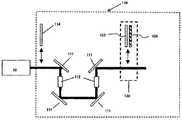
노광장치(1)는 도 1에 나타낸 바와 같이 조명장치(10); 레티클(20)을 탑재하는 레티클 스테이지; 투영 광학계(30); 웨이퍼(40)를 탑재하는 웨이퍼 스테이 지(45); 제어기(60); 및 검출기(70) 및 (80)를 포함한다.The
조명장치(10)는 전사될 회로 패턴을 지닌 피조명면으로서의 레티클(20)을 조명하고, 광원(12)과 조명 광학계(100)를 포함한다.The
광원(12)은 편광 조명에 있어서 95% 이상의 편광도를 갖는 레이저빔을 사출하는 것이 바람직하다. 따라서, 광원(12)은 파장 약 193 nm의 ArF 엑시머 레이저, 파장 약 248 nm의 KrF 엑시머 레이저를 사용한다. 단, 광원의 종류는 엑시머 레이저로 한정되지 않고, 파장 약 157 nm의 F2레이저를 사용할 수 있으며, 그 광원의 개수도 한정되지 않는다.The
조명 광학계(100)는 레티클(20)을 조명하기 위한 광학계이며, 렌즈, 미러, 광학 적분기 및 조리개를 포함한다. 본 실시형태의 조명 광학계(100)는 편향계(deflection system)(110), 광정형화 유닛(130), 광변환기(140), 결상 광학계(145), 집광광학계(160) 및 결상 광학계(170)를 포함한다. 또, 조명 광학계(100)는 파리의 눈렌즈(151), 조리개(152), 마스킹 블레이드(153), 필터 부재(154), σ형상 보정 기구(155) 및 위상판(159)을 더욱 포함한다.The illumination
도 2는 편향계(110)의 하나의 예시적인 구성을 나타낸 개략 단면도이다. 편향계(110)는 편향 미러(deflection mirror)(111), 원통형 렌즈(112), 위상판(114) 및 편광 조정 기구(120)를 포함한다. 편광 조정 기구(120)는 위상판(122), 편광 해소판(124) 및 개구판(도시 생략)을 포함하고, 광원(12)으로부터의 광의 광로(조명광학계(100)의 광로) 상에 이들을 선택적으로 배치한다.2 is a schematic cross-sectional view illustrating one exemplary configuration of the
편향계(110)에 있어서, 광원(12)으로부터 사출된 대략 편광광은 편향 미러(111)에 의해 편향되고, 원통형 렌즈(112)에 의해서 원 형상 또는 정방형 형상 등의 바람직한 형상 혹은 크기의 광으로 변경되어, 광정형화 유닛(130)에 도광된다.In the
편향계(110)는, 광축 시프트를 보정하기 위해서, 편향 미러(111)를 기울이거나 원통형 렌즈(112)를 편심시키도록 구성되어 있다. 본 실시형태의 편향계(110)는 입사광을 4번 편향시키는 구성이지만, 광원(12) 및 조명 광학계(100)의 배치에 따라, 다양한 편향 구성(편향 횟수나 편향 방법)을 적용할 수 있다.The
편향 미러(111)에 입사하는 광의 편광 상태는 편향 방법에 의해서 s-편광 또는 p-편광이 될 수 있다. 미러는 일반적으로 p-편광에 대한 반사율보다 s-편광에 대한 반사율이 높다. 그러므로, 미러에 입사하는 광 또는 미러에 반사되는 광을 s-편광으로 하면 조도와, 쓰루풋(throughput)이 향상한다고 하는 이점이 있다.The polarization state of the light incident on the
따라서, 본 실시형태는, 편향계(110)가 p-편광을 빈번하게 반사시키는 경우, 도 2에 나타낸 바와 같이, 광원(12)으로부터의 광이 입사하는 입사구에 위상판(114)을 배치하여, s-편광 반사가 많아지도록 한다. 또, 각 편향 미러에 s-편광이 입사하도록, 각 편향 미러 앞에 위상판을 배치해도 된다. 하지만, 위상판이 100%의 투과율을 소유하지 못하므로, 모든 편향 미러 앞에 위상판을 배치하는 것은 효과적이지 않다. 따라서, s-편광을 반사하는 편향 미러의 수가 많아지도록, 1개의 입사구에 위상판(114)을 배치하면 충분하다.Therefore, in this embodiment, when the
광정형화 유닛(130)에 입사하는 광의 편광 상태는 편향계(110)(위상판(114)) 에 의해서 조정된다. 또, 광정형화 유닛(130)에 입사하는 광의 편광 상태는 접선방향 편광이나 방사상 편광 등의 편광 조명의 종류에 따라 조정할 필요가 있다. 따라서, 편향계(110)는 편광 조정 기구(120)의 위상판(122)을 광로에 삽입할지 또는 해당 광로로부터 제거할지를 선택해서, 광정형화 유닛(130)에 입사하는 광의 편광 상태를 자유롭게 조정하도록 한다. 예를 들면, 위상판(122)으로서 λ/2판을 이용하여, 바람직한 편광 방향을 지닌 편광을 광정형화 유닛(130)에 입사시킨다. 또는, 위상판(122)으로서 λ/4판을 이용해도 된다.The polarization state of the light incident on the
또, 위상판(122)은 회전 가능하게 구성되어 편광도를 미세조정하는 데에도 이용된다. 후술하는 바와 같이, 검출부(70)가 간접적으로 노광량을 검출할 때, 2개의 편광 상태가 필요하다. 이러한 경우, 위상판(122)을 회전시킴으로써, 2개의 편광 상태를 형성할 수 있다. 또한, 랜덤 편광 조명의 경우에는 편향계(110)에 있어서 광원으로부터의 광의 광로 상에 편광 조정 기구(120)의 편광 해소판(124)을 배치한다(또는 위상판(122)을 편광 해소판(124)으로 교체한다).In addition, the
여기서, 조명장치(10)에 있어서의 위상판(114), (122) 및 (159)(이하, "본 실시형태의 위상판"이라고 칭함)의 구성에 대해 설명한다. 도 3A 및 도 3B는 본 실시형태의 위상판의 구성을 나타낸 도면으로, 도 3A는 본 실시형태의 위상판의 개략 단면도이며, 도 3B는 본 실시형태의 위상판의 개략 정면도이다.Here, the structure of the
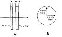
본 실시형태의 위상판은 도 3A에 나타낸 바와 같이 MgF2나 수정 등의 1축 결정으로 구성된 2개의 평판(PPa) 및 (PPb)을 포함하는 0차 위상판이지만, 1개의 평판 으로 구성된 n차 위상판을 이용해도 된다. 평판(PPa)의 두께와 평판(PPb)의 두께와의 사이에는 광을 수직으로 입사시켰을 때의 진상축(fast axis) 방향과 지상축(slow axis) 방향 간의 상대 위상차가 λ/2가 되도록 유리재 두께차 Δd가 있다. 본 실시형태에서는 평판(PPa)의 두께를 d, 평판(PPb)의 두께를 d+Δd로 설정하고 있다. (PPa) 및 (PPb)의 두께가 수 ㎛ 시프트되면, 위상차는 상당히 변화되어, 평판(PPa)과 평판(PPb) 간의 두께 차이인 유리재 두께차 Δd를 정확하게 형성할 필요가 있다. 도 3B는 도 3A에 나타낸 위상판을 조명 광학계의 광축 방향에서 본 도면이다. 도 3B에 있어서, 실선 화살표는 평판(PPa)의 진상축 방향을, 파선 화살표는 평판(PPb)의 진상축 방향을 나타내고 있다. 본 실시형태의 위상판은 평판(PPa)의 진상축과 평판(PPb)의 진상축 간의 각도를 90°로 유지한 상태로 배치된다.The phase plate of the present embodiment is a zero-order phase plate including two plates PPa and (PPb ) composed of uniaxial crystals such as MgF2 and quartz as shown in FIG. 3A, but is composed of one plate You may use an nth order phase plate. The relative phase difference between the fast axis direction and the slow axis direction when light is incident vertically between the thickness of the plate PPa and the thickness of the plate PPb is There is a glass thickness difference Δd. In this embodiment, the thickness of the flat plate PPa is set to d, and the thickness of the flat plate PPb is set to d + Δd. When the thicknesses of (PPa ) and (PPb ) are shifted by several micrometers, the phase difference is significantly changed, and it is necessary to accurately form the glass material thickness difference Δd which is the thickness difference between the plate PPa and the plate PPb . . 3B is a view of the phase plate shown in FIG. 3A seen in the optical axis direction of the illumination optical system. In FIG. 3B, the solid line arrow indicates the fast axis direction of the flat plate PPa , and the broken line arrow indicates the fast axis direction of the flat plate PPb . Phase plate of the present embodiment is disposed in a state of keeping the angle between the fast axes of the fast axis and the plate (PPb) of the plate (PPa) at 90 °.
도 4A 및 도 4B는, x-편광이 본 실시형태의 위상판에 입사했을 경우에, 위상판의 진상축 방향(위치)과 사출되는 광의 편광 상태와의 관계를 나타낸 도면이다. 도 4A에 나타낸 바와 같이, 입사 광의 편광 방향(x-편광)에 대해서 평판(PPa)의 진상축 방향이 0°로 되도록 위상판을 배치하면, x-편광이 사출된다. 한편, 도 4B에 나타낸 바와 같이, 입사 광의 편광 방향에 대해서 평판(PPa)의 진상축 방향이 45°로 되도록 위상판을 배치하면, y-편광이 사출된다. 또, 도 4C에 나타낸 바와 같이, 입사 광의 편광 방향에 대해서 평판(PPa)의 진상축 방향이 22.5°로 되도록 위상판을 배치하면, 45°편광이 사출된다.4A and 4B are diagrams showing the relationship between the fast-axis direction (position) of the phase plate and the polarization state of the emitted light when x-polarized light enters the phase plate of the present embodiment. As shown in Fig. 4A, when the phase plate is disposed so that the direction of the upward axis of the flat plate PPa becomes 0 ° with respect to the polarization direction (x-polarization) of the incident light, x-polarized light is emitted. On the other hand, as shown in FIG. 4B, whena phase plate is arrange | positioned so that the fast-axis direction of the flat plate PPa may be 45 degrees with respect to the polarization direction of incident light, y-polarization will be emitted. As shown in Fig. 4C, when the phase plate is arranged so that the fast axis direction of the flat plate PPa becomes 22.5 ° with respect to the polarization direction of the incident light, 45 ° polarized light is emitted.
특히, 고NA인 노광장치(1)에서는 평행광이 아니고, 소정의 각도 분포를 가지는 광이 위상판에 입사한다. 1축 결정으로 이루어진 2개의 평판으로 구성된 0차 위상판은 일반적으로 수직으로 입사하는 광(파장 λ(㎜))에 대해서, 소정의 위상차가 부여되도록, 2개의 위상판의 두께 d 및 d+Δd가 설정되어 있다. 단, 각도 θ로 광이 위상판에 입사했을 경우, 광이 위상판에 수직으로 입사했을 경우와 비교해서, 위상판으로의 광로 길이가 길어진다. 그 결과, 2개의 위상판을 통과한 후의 광은 이하의 수식 [1]로 표시되는 위상 오차 Δ를 포함해 버린다. 환언하면, 위상판은 각도 분포를 가지는 광에 대해서 소정의 위상차를 부여할 수 없다.In particular, in the

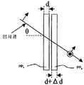
여기서, 도 5에 나타낸 바와 같이, 수정으로 이루어진 2개의 평판(PPa) 및 (PPb)으로 구성된 위상판(0차 1/2λ 파장판)을 상정한다. 또, 수정은 복굴절 유리재이며, 0.01364 ㎚/㎝의 복굴절량 Δn을 가진다. 또한, 도 5에 표시된 지면에 수직인 방향으로 전장 벡터가 진동하는 광의 강도를 Ix, 도 5의 지면에 평행한 방향으로 전장 벡터가 진동하는 광의 강도를 Iy라 할 때, 편광도를 Ix/(Ix+Iy)라고 정의한다.Here, as shown in Fig. 5, it is assumed the two flat plate made of a modified (PPa) and(b PP) phase plate (zero-
도 6은 도 5에 나타낸 위상판의 두께(또는 2개의 평판(PPa) 및 (PPb)의 두께 d(㎜) 및 d+Δd(㎜))와 편광도와의 관계를 나타낸다. 도 6에서는 가로축에 입사 광의 위상판에 대한 X방향의 입사각을, 세로축에 입사광의 위상판에 대한 Y방향의 입사각을 취하여, 편광도의 변화를 색의 농담으로 나타낸다. 덧붙여, X방향과 Y방향은 서로 수직이다. 도 6을 참조하면, 위상차 Δ는 입사각 θ 및 위상판의 두께에 의존하고, 입사각이 크면 클수록, 또, 위상판의 두께가 두꺼워지면 두꺼워질수록, 편광도의 변화가 큰 것을 알 수 있다.FIG. 6 shows the relationship between the thickness of the phase plate shown in FIG. 5 (or the thickness d (mm) and d + Δd (mm) of two flat plates PPa and PPb ) and the degree of polarization. In FIG. 6, the incident angle of the X direction with respect to the phase plate of incident light to a horizontal axis is taken, and the incident angle of the Y direction with respect to the phase plate of incident light to a vertical axis is taken, and the change of polarization degree is shown with the shade of color. In addition, the X direction and the Y direction are perpendicular to each other. Referring to FIG. 6, it can be seen that the phase difference Δ depends on the incident angle θ and the thickness of the phase plate, and the larger the angle of incidence and the thicker the thickness of the phase plate, the larger the change in polarization degree.
따라서, 본 실시형태의 위상판(복굴절량 Δn(㎚/㎜))은 입사광(파장 λ(㎚)를 지님)의 입사각 θ에 대해서, 이하의 수식 [2]를 만족하는 두께 d(㎜)를 가진다.Therefore, the phase plate (birefringence amount Δn (nm / mm)) of the present embodiment has a thickness d (mm) that satisfies the following formula [2] with respect to the incident angle θ of the incident light (having a wavelength λ (nm)). Have

도 6에 나타낸 원 안쪽의 영역 α는 수식 [2]를 만족시키는 영역이며, 95% 이상의 편광도를 만족시키는 조건이다.The region α inside the circle shown in FIG. 6 is a region that satisfies the formula [2], and is a condition that satisfies the degree of polarization of 95% or more.
도 7은 수식 [2]를 만족할 때의, 위상판의 두께와 입사각과의 관계를 나타낸 그래프이다. 본 실시형태는 유효 광원 형성 유닛에 입사하는 광의 편광 상태를 제어하는 위상판(114) 및 (122)과, 파리의 눈렌즈(151)에 입사하는 광의 편광 상태를 제어하는 위상판(159)을 가진다. 본 실시형태에서는 위상판(114) 및 (122)에 입사하는 광의 입사각 θ를 1°로 설정하고 있으므로, 위상판(114) 및 (122)의 두께는 11.6 ㎜ 이하로 유지되면 된다. 또, 위상판(159)에 입사하는 광의 입사각 θ는 3.0°이므로, 위상판(159)의 두께는 1.29 ㎜ 이하로 유지되면 된다. 덧붙여, 입사각 θ는 실제의 계측이나 광학계의 설계치로부터 산출될 수 있다.7 is a graph showing the relationship between the thickness of the phase plate and the incident angle when the expression [2] is satisfied. In this embodiment,
또, 본 실시형태에서 나타낸 위치 이외의 위치에 위상판을 배치하는 경우에서도, 위상판의 두께는 입사광의 입사각에 의해서 결정되는 두께와 동일 또는 그 이하의 두께로 하면 된다. 예를 들면, 유니포머(uniformer) 동공부, 혹은 조명 광학계 또는 투영 광학계의 동공면에 위상판을 배치하는 경우에도, 수식 [2]를 만족하는 한, 높은 편광 시프트를 발생시키는 일 없이 높은 편광도를 지닌 편광 조명이 가능해진다.Moreover, also when arrange | positioning a phase plate in positions other than the position shown by this embodiment, the thickness of a phase plate should just be thickness equal to or less than the thickness determined by the incident angle of incident light. For example, even when the phase plate is disposed in the uniform pupil part or in the pupil plane of the illumination optical system or the projection optical system, as long as the expression [2] is satisfied, a high polarization degree is not generated without generating a high polarization shift. With polarized light.
덧붙여, 수식 [1] 및 [2]로부터 알 수 있듯이, 위상판의 유리재의 복굴절량 Δn도 위상판의 두께를 결정하는 중요한 파라미터이다. 본 실시형태에서는 위상판의 유리재로서 복굴절량 Δn이 0.01367 ㎚/㎝인 수정을 이용하고 있지만, 그 이외의 유리재를 이용해도 된다. 예를 들면, 입사각이 더욱 큰 위치에 위상판을 배치하는 경우, 위상판의 두께가 얇아져서 그 제조가 곤란해질 것으로 여겨진다. 그 경우에는 위상판을 복굴절량이 작은 유리재로서 복굴절량 Δn이 0.008㎚/㎝인 사파이어를 이용해도 된다. 이것에 의해, 위상판의 두께의 허용 범위가 넓어져, 위상판의 제조가 용이해진다. 도 8은 위상판의 유리재로서 사파이어를 사용했을 경우, 수식 [2]를 만족할 때의 위상판의 두께와 입사각과의 관계를 나타낸 그래프이다. 도 7을 참조하면, 위상판의 유리재로서 수정을 사용했을 경우, 입사각 3°에서의 위상판의 두께의 허용 범위는 1.29(㎜)이다. 한편, 도 8을 참조하면, 위상판의 유리재로서 사파이어를 사용했을 경우, 입사각 3°에서의 위상판의 두께의 허용 범위는 2.2(㎜)이다. 즉, 위상판의 유리재로서 수정보다 사파이어를 이용하는 것이 위상판의 두께의 허용 범위가 넓어진다.In addition, as can be seen from equations [1] and [2], the birefringence amount Δn of the glass material of the phase plate is also an important parameter for determining the thickness of the phase plate. In this embodiment, although the birefringence amount (DELTA) n is 0.01367 nm / cm as a glass material of a phase plate, the glass material other than that may be used. For example, when arranging a phase plate in a position where an incident angle is larger, it is considered that the thickness of the phase plate becomes thin and manufacturing thereof becomes difficult. In that case, you may use sapphire whose birefringence amount (DELTA) n is 0.008 nm / cm as a glass material with a small birefringence amount. Thereby, the permissible range of the thickness of a phase plate becomes wide and manufacture of a phase plate becomes easy. 8 is a graph showing the relationship between the thickness of the phase plate and the incident angle when the sapphire is used as the glass material of the phase plate when the formula [2] is satisfied. Referring to FIG. 7, when the crystal is used as the glass material of the phase plate, the allowable range of the thickness of the phase plate at the incident angle of 3 ° is 1.29 (mm). On the other hand, referring to FIG. 8, when sapphire is used as a glass material of a phase plate, the permissible range of the thickness of a phase plate in incident angle of 3 degrees is 2.2 (mm). That is, the use of sapphire rather than quartz as the glass material of the phase plate widens the allowable range of the thickness of the phase plate.
또, 유리재의 내구성을 감안해서 위상판에 사용하는 유리재를 결정할 필요도 있다. 유리재의 내구성이 낮으면 복굴절량이 변화되어 버리므로, 정밀한 위상판을 구성할 수 없다. 예를 들면, 광강도가 강한 광이 입사하는 위상판은 내구성이 뛰어난 형석이나 MgF2로 만드는 것이 바람직하다.Moreover, in consideration of the durability of a glass material, it is also necessary to determine the glass material used for a phase plate. When the durability of the glass material is low, the birefringence amount is changed, so that a precise phase plate cannot be constituted. For example, it is preferable that the phase plate into which light with strong light intensity enters is made of fluorite or MgF2 which is excellent in durability.
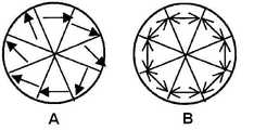
덧붙여, 위상판(159)은 파리의 눈렌즈(151) 앞에 배치되어, 유효 광원의 편광 상태를 바람직한 상태로 변경한다. 여기서, 유효 광원은 조명 광학계의 동공면에 있어서의 광강도 분포이며, 본 실시예에 있어서의 조명 광학계의 동공면은 파리의 눈렌즈(151)의 출사면이다. 도 10A 내지 도 11B는 위상판(159)의 예시적인 구성을 나타낸 개략 정면도이다. 도 10A 및 도 11A에서의 화살표는 위상판(159)의 진상축 방향이며, 도 10B 및 도 11B에서의 화살표는 편광 방향이다. 예를 들면, 위상판(159)이 유효 광원을 접선방향 편광으로 설정하는 경우, 입사 편광(x-편광)에 대해서, 도 10A에 나타낸 바와 같이, 8개의 위상판을 조합함으로써, 도 10B에 나타낸 팔각 접선방향 편광을 제공할 수 있다. 또, 크로스 폴(cross pole) 조명이 사각 접선방향 편광을 필요로 할 경우, 입사 편광(x-편광)에 대해서, 도 11A에 나타낸 바와 같이, 4개의 위상판을 조합함으로써, 도 11B에 나타낸 사각 접선방향 편광을 제공할 수 있다. 이와 같이, 위상판(159)은 본 실시예에서 개시된 것 이외의 조명 모드에 대해서도, 위상판의 조합을 통해서 유효 광원을 바람직한 편광 상태로 제공할 수 있다.In addition, the
상술한 것처럼, 위상판(159)에 입사하는 광의 입사각 θ는 3.0°이므로, 본 실시형태에서는 위상판(159)의 두께를 수식 [2]를 만족하도록 1.00(㎜)으로 설정하고 있다.As described above, since the incident angle θ of light incident on the
지금까지는 입사 편광이 x-편광이고, 위상판(159)이 접선방향 편광을 형성하는 것을 가정했지만, 입사 편광은 y-편광일 수도 있고, 방사상 편광(편광 방향이 방사상)이 형성될 수도 있다.So far, it has been assumed that the incident polarization is x-polarized light and the
도 1을 다시 참조하면, 광정형화 유닛(130)은 소정면(A면)에 있어서의 광의 형상이 원 형상, 고리형상(annular), 다중극 형상 등의 바람직한 형상을 갖도록 광원(12)으로부터의 광의 형상을 변환한다. 여기서 사용하는 A면은 유효 광원의 기본 형상을 형성하는 면이며, 그 기본 형상이 광변환기(140)에 의해서 변경된다. 또, 배율을 가변으로 하는 결상 광학계(145)에서 그 크기가 변경되어, 각 위치에 배치된 조리개(152) 등의 조리개 부재에 의해서 바람직한 유효 광원이 피조명 면 위에 형성된다.Referring back to FIG. 1, the
도 9는 광정형화 유닛(130)의 하나의 예시적인 구성을 나타낸 개략 단면도이다. 광정형화 유닛(130)은 파리의 눈렌즈, 내면 반사를 이용한 광학 파이프 또는 회절 광학 소자("DOE": diffraction optical element), 이들을 조합한 복수의 광학 적분기, 릴레이 광학계, 집광광학계 및 미러를 포함한다. 본 실시형태의 광정형화 유닛(130)은 광학 적분기(131) 및 (133); 광학계(132) 및 (135); 및 DOE(134a) 및 (134b)를 포함한다.9 is a schematic cross-sectional view showing one exemplary configuration of the
A면에 형성되는 패턴은 DOE(134a) 또는 (134b)의 푸리에 변환 패턴과 DOE(134a) 또는 (134b)에 입사하는 광의 각도 분포 사이의 소용돌이 형상 패턴이다. 덧붙여, 푸리에 변환 패턴이란 광을 수직, 또, NA=0으로 입사시켰을 때에 푸리에 변환면에 형성되는 패턴이다.The pattern formed on the A surface is a swirl pattern between the Fourier transform pattern of the
또, DOE(134a) 및 (134b)는 서로 교환 가능하게 구성된다. 예를 들면, DOE(134a) 및 (134b)를 교환함으로써, 원형상, 고리 형상, 다중극 형상 등의 다양한 분포를 A면 위에 형성할 수 있다. 또, DOE(134a) 및 (134b)는 4중극 등의 다중극에 있어서의 각 극의 영역의 강도가 다른 강도를 지니도록 하는 강도를 제공할 수도 있다.The
본 실시형태의 광정형화 유닛(130)은 유효 광원 형상을 형성하는 유닛으로서 DOE(134a) 및 (134b)를 이용하고 있지만, 프리즘 등의 편향 광학 부재를 이용해서 유효 광원을 형성해도 된다.Although the
광변환기(140)는 A면 근방에 배치되어 광정형화 유닛(130)에 의해서 기본 형상으로 변환된 광을 더욱 변경한다. 본 실시형태의 광변환기(140)는 원뿔형 광학 소자(142), 및 간격을 변경할 수 있는 원뿔형 광학 소자(144)를 가진다. 원뿔형 광학 소자(142)는 입사면이 오목형인 원뿔형 및 사출면이 볼록형인 원뿔형 광학 소자이며, 예를 들어, 고리 형상의 광을 A면에 형성한다. 또한, 광변환기(140)는 평행 평면판(도시 생략), 적당한 형상(예를 들면, 고리형상 개구, 4중극 개구, 원형 개구 등)의 조리개 부재, 사각뿔형 광학 소자, 지붕형 광학 소자, 배율을 변경하기 위한 확대/축소 빔 익스팬더(expander) 등을 가질 수 있다.The
광변환기(140)를 구성하는 복수의 광학 부재(본 실시형태에서는 원뿔형 광학 소자(142) 및 (144))는 교체 가능하게 광로 상에 배치될 수도 있고, 또는 복수의 광학 부재가 동시에 광축 상에 배치될 수도 있다. 또한, 광변환기(140)는 광로로부터 물러나 있을 수도 있다.A plurality of optical members (conical
파리의 눈렌즈(151)는 사출면 근방에 복수의 광원상(유효 광원)을 형성하여, 레티클(20)을 균일하게 조명한다. 복수의 광원상이 형성되는 B면 근방에는 개구경을 가변으로 하는 조리개(152)가 배치되어 있다. 단, 조리개(152)의 위치는 B면 근방으로 한정되지 않는다. 예를 들면, 조리개(152)는 광변환기(140)와 함께 터릿 등의 변환 수단에 의해서 선택적으로 A면에서의 광로에 삽입되어도 된다. 또, 조리개(152)는 파리의 눈렌즈(151)의 직전에 배치되어도 되고, 복수의 위치에 동시에 배치되어도 된다. 예를 들면, 방사 방향 또는 크기를 제한하는 방향으로 제한되는 일 없이, 사중극 등의 개구각만 변경 가능한 기구를 가지는 조리개를 광변환기(140)의 위치에 선택적으로 배치한다. 또한, 크기를 제한하는 홍채 조리개를 파리의 눈렌즈(151)의 직전에 배치함과 동시에, 선택적으로 고정 조리개를 B면에 배치한다. 이것에 의해, 바람직한 σ분포를 형성할 수 있다. 이와 같이, 상이한 기능을 분담한 복수의 조리개를 복수의 위치에 배치하고, 변경 또는 교체를 실시함으로써, 보다 다양한 σ조건을 실현할 수 있다.The fly's
조리개(152) 및 투영 광학계(30)의 개구 조리개(32)는 광학적으로 대략 공액인 위치에 배치된다. 파리의 눈렌즈(151) 및 조리개(152)에 의해서 형성되는 유효 광원의 개구 조리개(32)에 있어서의 형상이 웨이퍼(40) 위의 각 점에 있어서의 각도 분포에 대응한다.The
복수의 광원상으로부터의 광속 중 조리개(151)에 의해서 제한되지 않는 광은 집광광학계(160)를 개입시켜 마스킹 블레이드(153)의 면을 효율적으로 조명한다. 마스킹 블레이드(153)는 결상 광학계(170)를 개입시켜 레티클(20)의 면과 광학적으로 공액인 위치에 배치되어 레티클(20) 면 위에 있어서의 피조명 영역을 규정한다.Light that is not limited by the
본 실시형태의 집광광학계(160)는 렌즈(162) 및 (164)를 포함하고, 본 실시형태의 결상 광학계(170)는 렌즈(172) 및 (174)를 포함하지만, 이들에 있어서의 렌즈의 수는 한정되지 않는다.The light converging
집광광학계(160)에 있어서, 렌즈(162)와 (164) 사이에는 반투명경(166)이 배치되어 있다. 반투명경(166)은 입사하는 광을 반사광과 투과광으로 분할한다. 본 실시형태에서는 투과광은 레티클(20)을 조명하는 조명광으로서 사용하고, 반사광은 검출기(70)에서 노광량을 간접적으로 검출하기 위한 검출광으로서 사용한다. 덧붙여, 반투명경(166) 및 검출기(70)는 도 1에 나타낸 배치에 한정되지 않고, 광원(12)으로부터 마스킹 블레이드(153) 사이의 광로 중에 배치되어 있으면 된다.In the condensing
레티클(20)의 근방에는 레티클(20)과 투영 광학계(30) 사이에 광로에 대해서 삽입 및 인출되도록 검출기 (80)가 배치되어 있다. 상기 검출기(80)는 유효광원분포를 검출한다.In the vicinity of the
필터 부재(154)는 투과율 분포를 균일하게 하도록 배치된다. 환언하면, 필터 부재(154)는 투과막이나 반사막에 기인하는 투과율 분포의 불균일성을 소거시키는 투과율 분포를 가진다.The
σ형상 보정 기구(155)는 피조명면에 있어서의 σ분포를 이상적인 분포로 만든다. 특히, 편광 조명의 경우는 미러, 반투명경 및 반사 방지막에 기인하는 σ분포의 비대칭성이 발생하기 쉬워지기 때문에, σ형상 보정 기구(155)는 편광 상태의 변경에 따라 σ분포를 적절하게 조정한다.The sigma
유리재의 응력 복굴절은 상술한 것처럼 편광 시프트의 하나의 요인이며, 노광장치는 응력 복굴절을 낮게 유지하는 유리재를 이용할 필요가 있다. 그렇지만, 응력 복굴절을 낮게 유지하기 위해서는 특수한 제조 과정을 필요로 한다. 게다가, 제조에 장시간이 걸림과 동시에, 수율도 저하하므로, 유리재의 비용이 높아져 버린다. 따라서, 노광장치의 비용 저감과 바람직한 편광 상태를 확보하기 위해서, 모든 광학 소자에 대해서 낮은 응력 복굴절을 가진 유리재를 이용하는 것이 아니라, 배치하는 위치에 따라 유리재의 복굴절 규격을 바꾸는 것이 바람직하다.The stress birefringence of the glass material is one factor of the polarization shift as described above, and the exposure apparatus needs to use a glass material which keeps the stress birefringence low. However, maintaining a low stress birefringence requires a special manufacturing process. In addition, since the production takes a long time and the yield decreases, the cost of the glass material becomes high. Therefore, in order to reduce the cost of the exposure apparatus and to secure a preferable polarization state, it is preferable not to use a glass material having low stress birefringence for all the optical elements, but to change the birefringence standard of the glass material according to the arrangement position.
조명 광학계의 동공면보다 레티클(20) 측에 있어서의 편광 시프트는 유효 광원 내의 편광도 분포, 그리고 축상 광선과 축외 광선 간의 편광도의 편차를 일으킨다. 유효 광원내의 편광도 분포는 좌우 선폭(CD: Critical Dimention)차나 HV차를 발생시켜, 상 높이에서의 편광도의 차는 축상축외(axial-off-axial) CD차를 발생시킨다. 따라서, 조명 광학계의 동공면보다 레티클(20)에 가까운 유리재는 조명 광학계의 동공면보다 광원(12)에 가까운 유리재보다 복굴절량을 작게 할 필요가 있다.The polarization shift on the
도 12A는 조명 광학계의 동공면보다 레티클(20)에 가까운 유리재의 복굴절량을 변화시켰을 때의 콘트라스트의 변화를 나타낸 그래프이다. 도 12B는 조명 광 학계의 동공면보다 레티클(20)에 가까운 유리재의 복굴절량을 변화시켰을 때의 좌우 CD차의 변화를 나타낸 그래프이다. 도 12C는 조명 광학계의 동공면보다 레티클(20)에 가까운 유리재의 복굴절량을 변화시켰을 때의 축상축외 CD차를 나타낸 그래프이다. 또한, 도 12A 내지 도 12C는 조명 모드를 쌍극 조명으로 설정하고 있다. 도 12A 내지 도 12C를 참조하면, 복굴절량이 커짐에 따라, 콘트라스트, 좌우 CD차, 축상축외 CD차 등의 각 특성이 열화하고 있는 것을 알 수 있다. 이들 결과로부터, 조명 광학계의 동공면 뒤의 유리재의 복굴절량은 2(㎚/㎝) 이하를 유지하는 것이 바람직하다.12A is a graph showing a change in contrast when the birefringence amount of the glass material closer to the
한편, 조명 광학계의 동공면보다 광원(12)에 가까운 유리재의 복굴절량은 동공 전체면의 편광도를 일률적으로 저감시키지만, 유효 광원 내의 편광도 분포와, 축상 광선과 축외 광선 간의 편광도 편차에는 영향을 주지 않는다. 따라서, 조명 광학계의 동공면보다 광원(12)에 가까운 유리재는 콘트라스트의 저하를 일으킬 수 있지만, 좌우 CD차 및 축상축외 차의 열화에는 크게 영향을 주지 않기 때문에, 낮은 응력 복굴절을 지닌 유리재를 반드시 필요로 하지 않는다. 따라서, 조명 광학계의 동공면보다 광원(12)에 가까운 유리재의 복굴절량은 5(㎚/㎝) 이하이면 충분하다.On the other hand, the birefringence of the glass material closer to the
또한, 5(㎜) 이하의 두께의 유리재는 편광도의 시프트를 일으키는 일이 적고, 또 상 특성에 영향을 미치는 일이 적기 때문에, 위치에 관계없이 10(㎚/㎝) 이하의 복굴절량이면 충분하다.In addition, since a glass material having a thickness of 5 mm or less rarely causes a shift in polarization degree and rarely affects an image characteristic, a birefringence amount of 10 (nm / cm) or less is sufficient regardless of the position. .
또, 상술한 것처럼, 광강도가 강한 위치에 배치되는 유리재에는 뛰어난 내구 성을 가지는 형석이나 MgF2를 사용한다. 그렇지만, 형석 등의 불화물에는 IBR(진성 복굴절)이 존재하여, 그 영향으로 편광 시프트를 초래한다.As described above, fluorite or MgF2 having excellent durability is used for the glass material disposed at a position where the light intensity is strong. However, IBR (intrinsic birefringence) exists in fluorides, such as fluorite, and its influence causes a polarization shift.
도 13은 형석의 IBR에 의한 광의 전파 방향 의존성을 나타내고 있다. IBR은 <111>방향, <100>방향 및 이들과 등가인 방향으로 0이며, <110>방향 및 그것과 등가인 방향으로 최대가 된다. 따라서, IBR의 영향을 저감하기 위해서는 <111>방향 또는 <100>방향 혹은 그들의 등가 방향이 광축과 평행하도록, (111) 면 또는 (100) 면 혹은 그것과 등가인 면을 따라 자른 형석을 이용할 수 있다.Fig. 13 shows the dependence of the propagation direction of light on the IBR of fluorspar. IBR is 0 in the <111> direction, the <100> direction, and the direction equivalent to these, and becomes the largest in the <110> direction and the direction equivalent to it. Therefore, in order to reduce the influence of the IBR, the fluorite cut along the (111) plane or the (100) plane or the plane equivalent thereto can be used so that the <111> direction or the <100> direction or their equivalent direction is parallel to the optical axis. have.
단, 결정 방위(또는 결정축)를 <111>방향 또는 <100>방향에 가진 형석에 입사하는 광은 각도 분포를 가지고 있다. 따라서, 광은 <111>방향 또는 <100>방향으로부터 시프트되어, IBR의 영향을 받게 된다. 도 14A는 광축과 일치 혹은 평행한 결정 방위 <111>을 지닌 형석을 광의 입사 방향에서 본 도면이다. 도 14A에 나타낸 화살표는 <100>투영 벡터이며, 여기서, 형석의 모든 <100> 투영 벡터가 같은 위치를 지닌다. 도 14B는 조명 광학계 또는 투영 광학계의 동공면 내의 편광도를 나타낸 도면이다. 도 14B로부터 알 수 있는 바와 같이, IBR의 영향에 의해서 편광도가 국소적으로 시프트되고 있다. 이것은 IBR 분포가 같은 방향을 향하고 있으므로, 큰 IBR을 발생하는 위치가 각 유리재에서 일치하여, 유리재를 통과할 때마다 IBR의 영향을 크게 받는 몇몇 광속이 존재하기 때문이다.However, the light incident on the fluorite having the crystal orientation (or crystal axis) in the <111> direction or the <100> direction has an angular distribution. Therefore, the light is shifted from the <111> direction or the <100> direction, and is affected by the IBR. Fig. 14A is a view of fluorite having a crystal orientation <111> coincident with or parallel to the optical axis, as seen from the direction of incidence of light. The arrow shown in FIG. 14A is a <100> projection vector, where all <100> projection vectors of fluorite have the same position. 14B is a diagram showing the degree of polarization in the pupil plane of the illumination optical system or projection optical system. As can be seen from Fig. 14B, the polarization degree is locally shifted under the influence of the IBR. This is because the IBR distributions point in the same direction, so that the position where the large IBR is generated coincides in each glass material, so that there is some luminous flux that is greatly affected by the IBR each time it passes through the glass material.
따라서, 각 유리재가 IBR이 크게 발생하는 위치를 갖지 않도록 형석을 적절하게 회전시킬 경우, 이 영향을 회피할 수 있다. 도 15A는 광축과 일치 혹은 평 행한 결정 방위 <111>를 지닌 형석을 광의 입사 방향에서 본 도면이다. 도 15A에 표시된 화살표는 <100> 투영 벡터를 나타내며, 형석의 <100>투영 벡터가 상이한 경우를 나타내고 있다. 도 15B는 동공 내의 편광도를 도시하고 있다 도 15B로부터 알 수 있는 바와 같이, 동공 전체면에서 편광도가 시프트되지 않는다. 이와 같이, 형석의 회전 각도를 적절하게 조합함으로써, 편광 시프트를 저감시킬 수 있다.Therefore, this effect can be avoided when the fluorspar is appropriately rotated so that each glass member does not have a position where the IBR largely occurs. 15A is a view of fluorite having a crystal orientation <111> coincident with or parallel to the optical axis when viewed from the direction of incidence of light. Arrows shown in FIG. 15A indicate a <100> projection vector, and indicate a case where the <100> projection vector of fluorite is different. Fig. 15B shows the degree of polarization in the pupil. As can be seen from Fig. 15B, the degree of polarization does not shift in the entire pupil surface. Thus, polarization shift can be reduced by suitably combining the rotation angles of fluorite.
형석의 결정면 및 회전 각도를 최적화시켜도, 형석을 배치할 때의 경사각의 오차, 유리재를 자를 때의 각도 오차가 발생하여, 편광 시프트를 일으키는 것으로 생각된다. 편광 조명은 이러한 오차 요인도 가능한 한 작게 줄일 필요가 있다.Even if the crystal surface and the rotation angle of the fluorite are optimized, an error in the inclination angle when arranging the fluorite and an angular error when cutting the glass material are considered to cause polarization shift. Polarized illumination needs to reduce this error factor as small as possible.
도 16A는 형석의 결정 방위가 <111>방향 또는 <100>방향으로부터 경사지거나 또는 경사각 오차가 발생했을 경우를 나타내고 있다. 도 16A에 있어서, Θ는 <111>방향 또는 <100>방향에 대한 경사 각도이다. 도 16B는 경사각 오차에 대한 편광 시프트량을 나타낸 그래프이다. 도 16B로부터 알 수 있는 바와 같이, 경사각 Θ가 커짐에 따라서, 편광 시프트량도 증가한다. 도 16B로부터, 편광 조명 시에는 형석(유리재)의 경사각 오차를 ± 10° 이내로 유지하는 것이 바람직하다.FIG. 16A shows a case where the crystal orientation of the fluorite is inclined from the <111> direction or the <100> direction or an inclination angle error occurs. In FIG. 16A, Θ is an inclination angle with respect to the << 111> direction or the <100> direction. 16B is a graph showing the amount of polarization shift with respect to the tilt angle error. As can be seen from Fig. 16B, as the inclination angle Θ increases, the amount of polarization shift also increases. It is preferable from FIG. 16B to maintain the inclination angle error of fluorite (glass material) within +/- 10 degree at the time of polarized illumination.
또, 도 17A는 형석이 소정의 회전 각으로부터 시프트되거나 회전각 오차가 발생한 경우를 나타내고 있다. 도 17B는 회전각 오차에 대한 편광 시프트량을 나타내고 있다. 도 17B로부터 알 수 있는 바와 같이, 회전각 오차가 커짐에 따라서, 편광 시프트가 증가한다. 도 17B로부터, 편광 조명 시에는 회전각 오차를 ± 10°로 유지하는 것이 바람직하다.17A shows the case where the fluorite is shifted from a predetermined rotation angle or a rotation angle error occurs. 17B shows the amount of polarization shift with respect to the rotation angle error. As can be seen from Fig. 17B, as the rotation angle error becomes larger, the polarization shift increases. It is preferable from FIG. 17B to maintain the rotation angle error at +/- 10 degrees during polarized light illumination.
이하, 편광 조명에 필요한 반사막이나 투과막 등의 광학막의 특성에 대해 설명한다.Hereinafter, the characteristic of optical films, such as a reflective film and a transmission film which are necessary for polarized light illumination, is demonstrated.
조명 광학계의 동공면보다 레티클측에서는 미러에 입사하는 광의 입사각이 커지고, 이러한 미러 위의 반사막에 대한 s-편광과 p-편광 사이에 상당한 위상차가 생겨, 편광 시프트를 초래하게 된다. 따라서, 편광 조명에서는 미러에 입사하는 광의 최대 입사각을 45°± 10°이내로 유지하는 것이 바람직하다. 도 18A는 무편광 조명에 이용되는 산화막으로 이루어진 협대역 고반사 코팅("NBHR" 코팅: narrowband high-reflection coating)의 위상차의 각도 특성을 나타낸 그래프이다. 도 18B는 광대역의 입사각에서 위상차를 낮게 유지할 수 있는 Al층으로 이루어진 광대역 고반사 코팅("BBHR" 코팅: braodband high-reflection coating)의 위상차의 각도 특성을 나타낸 그래프이다.The angle of incidence of light incident on the mirror becomes larger on the reticle side than the pupil plane of the illumination optical system, and a significant phase difference occurs between s-polarized light and p-polarized light with respect to the reflective film on the mirror, resulting in a polarization shift. Therefore, in polarized light illumination, it is preferable to keep the maximum incidence angle of light incident on the mirror within 45 ° ± 10 °. 18A is a graph showing the angle characteristic of the phase difference of a narrowband high reflection coating ("NBHR" coating) consisting of an oxide film used for unpolarized illumination. 18B is a graph showing the angular characteristics of the phase difference of a broadband high reflection coating (“BBHR” coating: braodband high-reflection coating) composed of an Al layer capable of keeping the phase difference low at a wide angle of incidence of the broadband.
도 18A 및 도 18B를 참조하면, NBHR 코팅은 18°의 반사 위상차가 발생하고 있는 데 대해서, BBHR 코팅은 45° ± 10°의 입사각에 대해서 반사 위상차를 10°로 저감시키고 있다.18A and 18B, the NBHR coating has a reflection phase difference of 18 ° while the BBHR coating reduces the reflection phase difference to 10 ° for an incident angle of 45 ° ± 10 °.
도 19A는 x-편광, y-편광, 45°편광 및 -45°편광과 같은 NBHR 코팅의 각 편광 방향에 대한 동공 내의 편광 시프트의, 웨이퍼 면 위의 상점(0, 0), (13, 0) 및 (13, 4.5)에서 추정한 결과를 나타낸 도면이다. 도 19B는 x-편광, y-편광, 45°편광 및 -45°편광과 같은 BBHR 코팅의 각 편광 방향에 대한 동공 내의 편광 시프트의, 웨이퍼 면 위의 상점(0, 0), (13, 0) 및 (13, 4.5)에서 추정한 결과를 나타 낸 도면이다.FIG. 19A shows the shop (0, 0), (13, 0) on the wafer surface of the polarization shift in the pupil for each polarization direction of the NBHR coating, such as x-polarized, y-polarized, 45 ° polarized and -45 ° polarized. ) And (13, 4.5) show the result of estimation. 19B shows the shop (0, 0), (13, 0) on the wafer surface of the polarization shift in the pupil for each polarization direction of the BBHR coating, such as x-polarized, y-polarized, 45 ° polarized and -45 ° polarized. ) And (13, 4.5) show the result of estimation.
도 19A 및 도 19B로부터 알 수 있는 바와 같이, NBHR 코팅에서는 45°편광 및 -45°편광 양쪽에 대해서 편광이 상당히 시프트되고 있는 반면, BBHR 코팅에서는 각 편광 상태에서 편광 시프트량이 작다. 따라서, 조명 광학계의 동공면보다 레티클에 가까운 미러에 형성되는 반사막은 위상차를 ± 10°로 억제할 수 있는 동시에 알루미늄층을 포함하는 BBHR 코팅을 사용하는 것이 바람직하다.As can be seen from FIGS. 19A and 19B, the polarization shifts considerably for both 45 ° and −45 ° polarization in the NBHR coating, while the amount of polarization shift in each polarization state is small in the BBHR coating. Therefore, the reflective film formed on the mirror closer to the reticle than the pupil plane of the illumination optical system can suppress the phase difference to +/- 10 DEG and use a BBHR coating including an aluminum layer.
동공면보다 광원(12)에 가까운 조명 광학계는 편향 중에 광원(12)으로부터의 x-직선 편광을 유지한다. 단, 상술한 것처럼, 편광이 시프트될 수 있고, 또한, y-편광 성분이 발생할 수도 있다. x-편광 성분을 유지한 채로, y-편광 성분을 저감시켜, 시프트된 편광도를 회복하기 위해서는, s-편광에 대한 미러 반사율을 80% 이상으로 유지하는 것이 바람직하고, 또, p-편광에 대한 미러 반사율을 30% 이하로 유지하는 것이 바람직하다. 예를 들면, 95%의 편광도의 레이저광을 미러에 대해서 4번 반사시킨 경우를 가정한다. 여기서 상기 미러는 s-편광에 대한 반사율이 90%, p-편광에 대한 반사율이 30%인 반사 특성을 가지는 반사막을 갖는다. 이 경우, 편광도는 99.94%까지 회복될 수 있다. 또, 반사 방향에 따라서는 미러에 입사하는 광의 편광 상태가 y-편광 또는 p-편광일 수 있다. 이 경우, p-편광에 대한 미러 반사율은 80% 이상인 것이 바람직하고, s-편광에 대한 미러 반사율은 30%이하인 것이 바람직하다.The illumination optics closer to the
동공면보다 레티클에 가까운 조명 광학계는, 유효 광원을 형성하기 위해, 모든 편광 방향에 대해서 높은 반사율을 가지는 반사막을 필요로 한다. 따라서, s- 편광에 대한 미러 반사율은 90% 이상인 것이 바람직하고, p-편광에 대한 미러 반사율은 80% 이하인 것이 바람직하다.The illumination optical system closer to the reticle than the pupil plane requires a reflecting film having a high reflectance in all polarization directions in order to form an effective light source. Therefore, the mirror reflectance for s-polarized light is preferably 90% or more, and the mirror reflectance for p-polarized light is preferably 80% or less.
투과막의 s-편광 및 p-편광의 각각에 대한 반사율은 5% 이하로 구성하는 것이 바람직하다. 또, 투과막은 위상차를 3% 이내로 지니도록 구성하는 것이 바람직하다.It is preferable that the reflectance of each of the s-polarized light and the p-polarized light of the transmission membrane is 5% or less. In addition, the permeable membrane is preferably configured to have a phase difference within 3%.
도 20은 투과막의 위상차의 각도 특성을 나타낸 그래프이다. 도 20을 참조하면, 본 실시형태에서는 최대 입사각을 45°로, 최대 위상차를 3°로 설정하고 있다.20 is a graph showing the angle characteristic of the phase difference of the permeable membrane. 20, in this embodiment, the maximum incident angle is set to 45 degrees and the maximum phase difference is set to 3 degrees.
도 21은 투과막의 x-편광, y-편광, 45°편광 및 -45°편광 등의 각 편광 방향에 대한 동공 내의 편광 시프트를, 웨이퍼 면 위의 상점(0, 0), (13, 0) 및 (13, 4.5)에서 추정한 결과를 나타낸 도면이다. 도 21을 참조하면, 편광 시프트는 거의 발생하고 있지 않다.Fig. 21 shows the polarization shift in the pupil for each polarization direction such as x-polarized light, y-polarized light, 45 ° polarized light and -45 ° polarized light of the transmission membrane, on the wafer surface (0, 0), (13, 0) And (13, 4.5) show the result of estimation. Referring to FIG. 21, polarization shift hardly occurs.
다시, 도 1로 되돌아오면, 레티클(20)은 석영으로 이루어지고, 그 위에 전사되어야 할 회로 패턴을 갖고 있다. 레티클 스테이지(도시 생략)는 레티클(20)을 지지 및 구동한다.1, the
투영 광학계(30)는 레티클(20)의 패턴을 웨이퍼(40) 위에 투영하는 광학계이다. 이 투영 광학계(30)는 개구 조리개(32)를 가져, 임의의 개구수(NA)를 설정할 수 있다. 개구 조리개(32)는 웨이퍼(40)에 있어서의 결상 광의 NA를 결정하는 개구 직경을 가변으로 해서, 필요에 따라서 개구 직경이 변경된다. 본 실시형태의 간섭 인자 σ는 파리의 눈렌즈(151)에 의해 형성되는 복수의 광원의 개구 조리 개(32)의 위치에서의 상의 크기와 개구 조리개(32)의 개구 직경 간의 비율이다.The projection
B면(상부에 복수의 다광원이 형성되는 면)과 개구 조리개(32)는 서로 광학적으로 대략 공액이다. 실질적으로, B면에서의 분포가 웨이퍼(40)에 있어서의 σ분포 또는 유효 광원을 결정한다. 조리개(152)가 B면에 배치되어 있는 경우, σ분포는 조리개(152)에 의해서 제한되지 않는 분포이다. 조리개(152)가 B면에 배치되고, 또, 파리의 눈렌즈(151)가 충분히 미세한 렌즈(예를 들면, 1 방향으로 수십열 이상)로 구성된 경우, 실질적인 σ분포는 광정형화 유닛(130) 및 광변환기(140)를 개입시켜 형성된 파리의 눈렌즈(151)의 입사면에서의 분포이다.Surface B (surface in which a plurality of light sources are formed) and the
본 실시형태의 투영 광학계(30)는 복수의 렌즈(34) 및 (36)를 포함하는 굴절계이지만, 반사 굴절계(카타디옵트릭 광학계) 또는 반사계를 사용해도 된다. 최근 주목받고 있는 액침 리소그래피에서는 투영 광학계(30)의 최종 광학 소자와 웨이퍼(40) 사이에 순수 등의 액체를 채우고 있다. 이러한 소위 액침 노광장치에서는 고 NA로 노광하므로, 편광 제어의 효과가 특히 크다.The projection
본 실시형태의 기판은 웨이퍼이지만, 유리 기판이나 그 외의 기판을 넓게 포함한다. 웨이퍼(40)의 표면에는 포토레지스트가 도포되어 있다.Although the board | substrate of this embodiment is a wafer, it includes a glass substrate and other board | substrates widely. Photoresist is applied to the surface of the
웨이퍼 스테이지(45)는 웨이퍼 척(도시생략)을 개입시키고, 웨이퍼(40)를 지지한다. 웨이퍼 스테이지(45)는 당업계에 주지된 어떠한 구성도 적용할 수 있으므로, 여기에서는 그 설명은 생략한다.The
제어기(60)는 CPU 및 메모리를 구비하고, 노광장치(1)의 동작을 제어한다. 제어기(60)는 노광장치(1)의 각 구성 부재, 예를 들어, 조명장치(10), 레티클 스테 이지, 웨이퍼 스테이지(45), 검출기(70) 및 (80), 및 σ형상 보정 기구(155) 등과 제어 가능하게 접속한다.The
노광시, 광원(12)으로부터 발사된 광은 조명 광학계(100)를 개입시켜 레티클(20)을 조명한다. 레티클(20)의 패턴을 통과한 광은 투영 광학계(30)에 의해 웨이퍼(40)에 결상된다. 노광장치(1)는 복수의 위상판(114), (122) 및 (159)에 의해서 소망의 편광 상태를 형성할 수 있다. 또, 이러한 복수의 위상판은 수식 [2]를 만족하는 구성이므로, 웨이퍼(40) 면에서의 편광 상태를 바람직한 편광 상태의 80% 이상으로 유지할 수 있다. 또, 노광장치(1)에 있어서, 편광 시프트를 일으키는 유리재의 복굴절량 및 광학막의 특성도, 웨이퍼(40) 면에서의 편광 상태를 소망의 편광 상태의 80% 이상으로 유지할 수 있다. 환언하면, 노광장치(1)는 웨이퍼(40) 면에 있어서의 편광 상태를 소망의 상태로 유지할 수 있고, 특히, NA를 가지는 광에 대해서도 편광 상태를 정밀하게 제어할 수 있다. 이것에 의해, 노광장치(1)는 고해상도 및 고콘트라스트를 실현할 수 있어 높은 쓰루풋 및 경제적인 효율로 반도체 디바이스나 액정 표시 디바이스 등의 디바이스를 제조할 수 있다.Upon exposure, light emitted from the
다음에, 도 23 및 도 24를 참조해서, 상기 노광장치(1)를 이용한 디바이스 제조방법에 대해 설명한다. 도 23은 반도체 디바이스나 액정 표시 디바이스 등의 디바이스의 제조를 설명하기 위한 순서도이다. 여기서는 반도체 디바이스의 제조를 일례로서 설명한다. 스텝 1(회로설계)에서는 반도체 디바이스 회로를 설계한다. 스텝 2(레티클 제작)에서는 설계한 회로패턴을 지닌 레티클을 형성한다. 스텝 3(웨이퍼 제조)에서는 실리콘 등의 재료를 이용해서 웨이퍼를 제조한다. 스 텝 4(웨이퍼 프로세스)는 전(前)공정으로도 불리며, 레티클과 웨이퍼를 이용해서 포토리소그라피에 의해 웨이퍼 위에 실제의 회로를 형성한다. 스텝 5(조립)는 후공정으로도 불리며, 스텝 4에서 형성된 웨이퍼를 반도체칩으로 형성하는 공정이고, 어셈블리 공정(예를 들면, 다이싱, 본딩), 패키징 공정(칩밀봉) 등을 포함한다. 스텝 6(검사)에서는 스텝 5에서 작성된 반도체 디바이스의 확인시험, 내구성 시험 등의 각종 검사를 행한다. 이들 스텝을 통해서, 반도체 디바이스가 완성되어 출하된다(스텝 7).Next, with reference to FIG. 23 and FIG. 24, the device manufacturing method using the said
도 24는 상기 웨이퍼 프로세스의 상세한 순서도이다. 스텝 11(산화)에서는 웨이퍼 표면을 산화시킨다. 스텝 12(CVD)에서는 웨이퍼 표면에 절연막을 형성한다. 스텝 13(전극형성)에서는 웨이퍼 위에 전극을 증착법 등에 의해 형성한다. 스텝 14(이온주입)에서는 웨이퍼에 이온을 주입한다. 스텝 15(레지스트 처리)에서는 웨이퍼에 감광재를 도포한다. 스텝 16(노광)에서는 상기 노광방법을 이용해서 레티클의 회로 패턴을 웨이퍼에 노광한다. 스텝 17(현상)에서는 노광된 웨이퍼를 현상한다. 스텝 18(에칭)에서는 현상된 레지스트상 이외의 부분을 에칭한다. 스텝 19(레지스트 박리)에서는 에칭이 끝나 불필요하게 된 레지스트를 제거한다. 이들 스텝을 반복해서 행함으로써, 웨이퍼 위에 다층의 회로패턴을 형성한다.24 is a detailed flowchart of the wafer process. In step 11 (oxidation), the wafer surface is oxidized. In step 12 (CVD), an insulating film is formed on the wafer surface. In step 13 (electrode formation), an electrode is formed on the wafer by vapor deposition or the like. In step 14 (ion implantation), ions are implanted into the wafer. In step 15 (resist process), a photosensitive material is applied to the wafer. In step 16 (exposure), the circuit pattern of the reticle is exposed to the wafer using the above exposure method. In step 17 (development), the exposed wafer is developed. Step 18 (etching) etches parts other than the developed resist image. In step 19 (resist stripping), the resist which is not required after etching is removed. By repeating these steps, a multilayer circuit pattern is formed on the wafer.
이상, 본 발명에 의하면, 피조명면에 있어서의 편광 상태를 바람직한 상태로 유지할 수 있는, 즉, 각도 분포를 가지는 광에 대해서도 편광 상태를 정밀하게 제 어할 수 있는 조명 광학계를 제공하는 것이 가능하다.As mentioned above, according to this invention, it is possible to provide the illumination optical system which can maintain the polarization state in a to-be-lighted surface to a preferable state, ie, can control the polarization state precisely also with respect to the light which has an angular distribution.
2006년 3월 24일자로 출원된 일본 특허출원 제2006-083485호에 개시된 청구범위, 명세서, 도면 및 요약을 포함한 전체 내용은 참조로 전체로서 본 출원에 원용한다.The entire contents, including claims, specification, drawings and summaries disclosed in Japanese Patent Application No. 2006-083485, filed March 24, 2006, are incorporated herein by reference in their entirety.
본 발명의 정신과 범위를 일탈함이 없이 본 발명의 다수의 명백하게 광범위한 다른 실시형태를 실행할 수 있으므로, 본 발명은 이하의 특허청구범위에 규정된 것을 제외하고 그의 구체적인 실시형태로 한정되지 않는다.As many apparently widely different embodiments of the present invention can be made without departing from the spirit and scope thereof, it is to be understood that the invention is not limited to the specific embodiments thereof except as defined in the following claims.
Claims (11)
Translated fromKorean
Applications Claiming Priority (2)
| Application Number | Priority Date | Filing Date | Title |
|---|---|---|---|
| JP2006083485AJP2007258575A (en) | 2006-03-24 | 2006-03-24 | Illumination apparatus, exposure apparatus having the illumination apparatus, and device manufacturing method |
| JPJP-P-2006-00083485 | 2006-03-24 |
Publications (2)
| Publication Number | Publication Date |
|---|---|
| KR20070096936A KR20070096936A (en) | 2007-10-02 |
| KR100871016B1true KR100871016B1 (en) | 2008-11-27 |
Family
ID=38533010
Family Applications (1)
| Application Number | Title | Priority Date | Filing Date |
|---|---|---|---|
| KR1020070029097AExpired - Fee RelatedKR100871016B1 (en) | 2006-03-24 | 2007-03-26 | Illumination apparatus, exposure apparatus having the same, and device manufacturing method |
Country Status (4)
| Country | Link |
|---|---|
| US (1) | US20070222963A1 (en) |
| JP (1) | JP2007258575A (en) |
| KR (1) | KR100871016B1 (en) |
| TW (1) | TW200745726A (en) |
Families Citing this family (7)
| Publication number | Priority date | Publication date | Assignee | Title |
|---|---|---|---|---|
| JP5319766B2 (en)* | 2008-06-20 | 2013-10-16 | カール・ツァイス・エスエムティー・ゲーエムベーハー | Optical system of microlithography projection exposure apparatus and microlithography exposure method |
| JP5185727B2 (en)* | 2008-08-22 | 2013-04-17 | ギガフォトン株式会社 | Polarization purity control device and gas laser device having the same |
| JP5595015B2 (en)* | 2009-11-16 | 2014-09-24 | キヤノン株式会社 | Projection optical system, exposure apparatus, and device manufacturing method |
| DE102009055184B4 (en) | 2009-12-22 | 2011-11-10 | Carl Zeiss Smt Gmbh | Optical system, in particular a microlithographic projection exposure apparatus |
| JP2012191148A (en)* | 2011-03-14 | 2012-10-04 | Ricoh Co Ltd | Surface-emitting laser module, optical scanning device, and image forming device |
| WO2013042679A1 (en)* | 2011-09-19 | 2013-03-28 | 株式会社ニコン | Illuminating optical device, optical system unit, illumination method, and light exposure method and device |
| CN114047137B (en)* | 2021-09-28 | 2023-09-12 | 深圳市麓邦技术有限公司 | Polarization information conversion or duplication splicing method |
Citations (6)
| Publication number | Priority date | Publication date | Assignee | Title |
|---|---|---|---|---|
| JPH0587728A (en)* | 1991-08-23 | 1993-04-06 | Fuoto Device Kk | Polarized light analyzing method and ellipsometer using it |
| JPH07280649A (en)* | 1994-04-11 | 1995-10-27 | Sumitomo Metal Mining Co Ltd | Optical waveguide type polarization detector |
| JP2004145217A (en) | 2002-10-28 | 2004-05-20 | Sharp Corp | Projection type image display device |
| WO2005041277A1 (en) | 2003-10-28 | 2005-05-06 | Nikon Corporation | Lighting optical device and projection aligner |
| JP2005321562A (en) | 2004-05-07 | 2005-11-17 | Canon Inc | Polarization separating element and optical system having the same |
| US20060055834A1 (en) | 2002-12-03 | 2006-03-16 | Nikon Corporation | Illumination optical system, exposure apparatus, and exposure method |
Family Cites Families (5)
| Publication number | Priority date | Publication date | Assignee | Title |
|---|---|---|---|---|
| DE10124566A1 (en)* | 2001-05-15 | 2002-11-21 | Zeiss Carl | Optical imaging system with polarizing agents and quartz crystal plate therefor |
| JP2003090978A (en)* | 2001-09-17 | 2003-03-28 | Canon Inc | Illumination apparatus, exposure apparatus, and device manufacturing method |
| US7170574B2 (en)* | 2003-12-11 | 2007-01-30 | Jds Uniphase Corporation | Trim retarders incorporating negative birefringence |
| JP4776891B2 (en)* | 2004-04-23 | 2011-09-21 | キヤノン株式会社 | Illumination optical system, exposure apparatus, and device manufacturing method |
| US7548370B2 (en)* | 2004-06-29 | 2009-06-16 | Asml Holding N.V. | Layered structure for a tile wave plate assembly |
- 2006
- 2006-03-24JPJP2006083485Apatent/JP2007258575A/enactivePending
- 2007
- 2007-03-23USUS11/690,315patent/US20070222963A1/ennot_activeAbandoned
- 2007-03-26KRKR1020070029097Apatent/KR100871016B1/ennot_activeExpired - Fee Related
- 2007-03-26TWTW096110411Apatent/TW200745726A/enunknown
Patent Citations (6)
| Publication number | Priority date | Publication date | Assignee | Title |
|---|---|---|---|---|
| JPH0587728A (en)* | 1991-08-23 | 1993-04-06 | Fuoto Device Kk | Polarized light analyzing method and ellipsometer using it |
| JPH07280649A (en)* | 1994-04-11 | 1995-10-27 | Sumitomo Metal Mining Co Ltd | Optical waveguide type polarization detector |
| JP2004145217A (en) | 2002-10-28 | 2004-05-20 | Sharp Corp | Projection type image display device |
| US20060055834A1 (en) | 2002-12-03 | 2006-03-16 | Nikon Corporation | Illumination optical system, exposure apparatus, and exposure method |
| WO2005041277A1 (en) | 2003-10-28 | 2005-05-06 | Nikon Corporation | Lighting optical device and projection aligner |
| JP2005321562A (en) | 2004-05-07 | 2005-11-17 | Canon Inc | Polarization separating element and optical system having the same |
Also Published As
| Publication number | Publication date |
|---|---|
| TW200745726A (en) | 2007-12-16 |
| KR20070096936A (en) | 2007-10-02 |
| JP2007258575A (en) | 2007-10-04 |
| US20070222963A1 (en) | 2007-09-27 |
Similar Documents
| Publication | Publication Date | Title |
|---|---|---|
| EP1602981B1 (en) | Illumination optical system and exposure apparatus | |
| KR101737682B1 (en) | Illuminating optical apparatus, exposure apparatus, and device manufacturing method | |
| KR0137348B1 (en) | Refflection and refraction optical system and projection exposure apparatus using the same | |
| KR100856976B1 (en) | Exposure apparatus and device manufacturing method | |
| KR101083926B1 (en) | Exposure method, device manufacturing method, and illumination optical system | |
| KR100674045B1 (en) | Lighting device, exposure device and device manufacturing method | |
| KR100871016B1 (en) | Illumination apparatus, exposure apparatus having the same, and device manufacturing method | |
| US7602474B2 (en) | Exposure apparatus | |
| JP4095376B2 (en) | Exposure apparatus and method, and device manufacturing method | |
| US7955765B2 (en) | Adjustment method, exposure method, device manufacturing method, and exposure apparatus | |
| US8576378B2 (en) | Illumination optical system, exposure apparatus, and device manufacturing method | |
| US7126673B2 (en) | Illumination optical system and exposure apparatus having the same | |
| US20090040497A1 (en) | Exposure apparatus, adjusting method, exposure method, and device fabrication method | |
| JP3673731B2 (en) | Exposure apparatus and method | |
| JP2007189079A (en) | Illumination optical system, exposure apparatus having the illumination optical system, and device manufacturing method | |
| JP5225433B2 (en) | Illumination optical system and exposure apparatus | |
| JP2000091219A (en) | Position detecting apparatus and exposure apparatus using the same | |
| JP4581743B2 (en) | Illumination optical apparatus, exposure apparatus, and microdevice manufacturing method | |
| JP2009094350A (en) | Exposure apparatus and correction apparatus | |
| WO2005078778A1 (en) | Lighting optical device, polarization status detector,and exposure system and exposure method | |
| HK1130091B (en) | Exposure device of projector, exposure method and device manufacturing method |
Legal Events
| Date | Code | Title | Description |
|---|---|---|---|
| A201 | Request for examination | ||
| PA0109 | Patent application | St.27 status event code:A-0-1-A10-A12-nap-PA0109 | |
| PA0201 | Request for examination | St.27 status event code:A-1-2-D10-D11-exm-PA0201 | |
| D13-X000 | Search requested | St.27 status event code:A-1-2-D10-D13-srh-X000 | |
| PG1501 | Laying open of application | St.27 status event code:A-1-1-Q10-Q12-nap-PG1501 | |
| D14-X000 | Search report completed | St.27 status event code:A-1-2-D10-D14-srh-X000 | |
| E902 | Notification of reason for refusal | ||
| PE0902 | Notice of grounds for rejection | St.27 status event code:A-1-2-D10-D21-exm-PE0902 | |
| T11-X000 | Administrative time limit extension requested | St.27 status event code:U-3-3-T10-T11-oth-X000 | |
| E13-X000 | Pre-grant limitation requested | St.27 status event code:A-2-3-E10-E13-lim-X000 | |
| P11-X000 | Amendment of application requested | St.27 status event code:A-2-2-P10-P11-nap-X000 | |
| P13-X000 | Application amended | St.27 status event code:A-2-2-P10-P13-nap-X000 | |
| E701 | Decision to grant or registration of patent right | ||
| PE0701 | Decision of registration | St.27 status event code:A-1-2-D10-D22-exm-PE0701 | |
| R18-X000 | Changes to party contact information recorded | St.27 status event code:A-3-3-R10-R18-oth-X000 | |
| GRNT | Written decision to grant | ||
| PR0701 | Registration of establishment | St.27 status event code:A-2-4-F10-F11-exm-PR0701 | |
| PR1002 | Payment of registration fee | St.27 status event code:A-2-2-U10-U11-oth-PR1002 Fee payment year number:1 | |
| PG1601 | Publication of registration | St.27 status event code:A-4-4-Q10-Q13-nap-PG1601 | |
| R17-X000 | Change to representative recorded | St.27 status event code:A-5-5-R10-R17-oth-X000 | |
| R17-X000 | Change to representative recorded | St.27 status event code:A-5-5-R10-R17-oth-X000 | |
| PR1001 | Payment of annual fee | St.27 status event code:A-4-4-U10-U11-oth-PR1001 Fee payment year number:4 | |
| FPAY | Annual fee payment | Payment date:20121023 Year of fee payment:5 | |
| PR1001 | Payment of annual fee | St.27 status event code:A-4-4-U10-U11-oth-PR1001 Fee payment year number:5 | |
| FPAY | Annual fee payment | Payment date:20131029 Year of fee payment:6 | |
| PR1001 | Payment of annual fee | St.27 status event code:A-4-4-U10-U11-oth-PR1001 Fee payment year number:6 | |
| FPAY | Annual fee payment | Payment date:20141028 Year of fee payment:7 | |
| PR1001 | Payment of annual fee | St.27 status event code:A-4-4-U10-U11-oth-PR1001 Fee payment year number:7 | |
| FPAY | Annual fee payment | Payment date:20151023 Year of fee payment:8 | |
| PR1001 | Payment of annual fee | St.27 status event code:A-4-4-U10-U11-oth-PR1001 Fee payment year number:8 | |
| FPAY | Annual fee payment | Payment date:20161025 Year of fee payment:9 | |
| PR1001 | Payment of annual fee | St.27 status event code:A-4-4-U10-U11-oth-PR1001 Fee payment year number:9 | |
| FPAY | Annual fee payment | Payment date:20171025 Year of fee payment:10 | |
| PR1001 | Payment of annual fee | St.27 status event code:A-4-4-U10-U11-oth-PR1001 Fee payment year number:10 | |
| PR1001 | Payment of annual fee | St.27 status event code:A-4-4-U10-U11-oth-PR1001 Fee payment year number:11 | |
| PR1001 | Payment of annual fee | St.27 status event code:A-4-4-U10-U11-oth-PR1001 Fee payment year number:12 | |
| PR1001 | Payment of annual fee | St.27 status event code:A-4-4-U10-U11-oth-PR1001 Fee payment year number:13 | |
| PR1001 | Payment of annual fee | St.27 status event code:A-4-4-U10-U11-oth-PR1001 Fee payment year number:14 | |
| PR1001 | Payment of annual fee | St.27 status event code:A-4-4-U10-U11-oth-PR1001 Fee payment year number:15 | |
| PC1903 | Unpaid annual fee | St.27 status event code:A-4-4-U10-U13-oth-PC1903 Not in force date:20231122 Payment event data comment text:Termination Category : DEFAULT_OF_REGISTRATION_FEE | |
| PC1903 | Unpaid annual fee | St.27 status event code:N-4-6-H10-H13-oth-PC1903 Ip right cessation event data comment text:Termination Category : DEFAULT_OF_REGISTRATION_FEE Not in force date:20231122 |