KR100870660B1 - Liquid crystal display device and manufacturing method with improved adhesion of panel - Google Patents
Liquid crystal display device and manufacturing method with improved adhesion of panelDownload PDFInfo
- Publication number
- KR100870660B1 KR100870660B1KR1020010089306AKR20010089306AKR100870660B1KR 100870660 B1KR100870660 B1KR 100870660B1KR 1020010089306 AKR1020010089306 AKR 1020010089306AKR 20010089306 AKR20010089306 AKR 20010089306AKR 100870660 B1KR100870660 B1KR 100870660B1
- Authority
- KR
- South Korea
- Prior art keywords
- sealing
- protective layer
- insulating layer
- liquid crystal
- region
- Prior art date
- Legal status (The legal status is an assumption and is not a legal conclusion. Google has not performed a legal analysis and makes no representation as to the accuracy of the status listed.)
- Expired - Fee Related
Links
Images


Classifications
- G—PHYSICS
- G02—OPTICS
- G02F—OPTICAL DEVICES OR ARRANGEMENTS FOR THE CONTROL OF LIGHT BY MODIFICATION OF THE OPTICAL PROPERTIES OF THE MEDIA OF THE ELEMENTS INVOLVED THEREIN; NON-LINEAR OPTICS; FREQUENCY-CHANGING OF LIGHT; OPTICAL LOGIC ELEMENTS; OPTICAL ANALOGUE/DIGITAL CONVERTERS
- G02F1/00—Devices or arrangements for the control of the intensity, colour, phase, polarisation or direction of light arriving from an independent light source, e.g. switching, gating or modulating; Non-linear optics
- G02F1/01—Devices or arrangements for the control of the intensity, colour, phase, polarisation or direction of light arriving from an independent light source, e.g. switching, gating or modulating; Non-linear optics for the control of the intensity, phase, polarisation or colour
- G02F1/13—Devices or arrangements for the control of the intensity, colour, phase, polarisation or direction of light arriving from an independent light source, e.g. switching, gating or modulating; Non-linear optics for the control of the intensity, phase, polarisation or colour based on liquid crystals, e.g. single liquid crystal display cells
- G02F1/133—Constructional arrangements; Operation of liquid crystal cells; Circuit arrangements
- G02F1/1333—Constructional arrangements; Manufacturing methods
- G02F1/1339—Gaskets; Spacers; Sealing of cells
- G—PHYSICS
- G02—OPTICS
- G02F—OPTICAL DEVICES OR ARRANGEMENTS FOR THE CONTROL OF LIGHT BY MODIFICATION OF THE OPTICAL PROPERTIES OF THE MEDIA OF THE ELEMENTS INVOLVED THEREIN; NON-LINEAR OPTICS; FREQUENCY-CHANGING OF LIGHT; OPTICAL LOGIC ELEMENTS; OPTICAL ANALOGUE/DIGITAL CONVERTERS
- G02F1/00—Devices or arrangements for the control of the intensity, colour, phase, polarisation or direction of light arriving from an independent light source, e.g. switching, gating or modulating; Non-linear optics
- G02F1/01—Devices or arrangements for the control of the intensity, colour, phase, polarisation or direction of light arriving from an independent light source, e.g. switching, gating or modulating; Non-linear optics for the control of the intensity, phase, polarisation or colour
- G02F1/13—Devices or arrangements for the control of the intensity, colour, phase, polarisation or direction of light arriving from an independent light source, e.g. switching, gating or modulating; Non-linear optics for the control of the intensity, phase, polarisation or colour based on liquid crystals, e.g. single liquid crystal display cells
- G02F1/133—Constructional arrangements; Operation of liquid crystal cells; Circuit arrangements
- G02F1/136—Liquid crystal cells structurally associated with a semi-conducting layer or substrate, e.g. cells forming part of an integrated circuit
- G02F1/1362—Active matrix addressed cells
- G02F1/136227—Through-hole connection of the pixel electrode to the active element through an insulation layer
Landscapes
- Physics & Mathematics (AREA)
- Nonlinear Science (AREA)
- Mathematical Physics (AREA)
- Chemical & Material Sciences (AREA)
- Crystallography & Structural Chemistry (AREA)
- General Physics & Mathematics (AREA)
- Optics & Photonics (AREA)
- Liquid Crystal (AREA)
Abstract
Translated fromKoreanDescription
Translated fromKorean도 1은 일반적인 액정표시소자의 구조를 나타내는 평면도.1 is a plan view showing the structure of a general liquid crystal display device.
도 2는 종래 액정표시소자의 화소영역 및 실링영역의 구조를 나타내는 단면도.2 is a cross-sectional view showing the structure of a pixel region and a sealing region of a conventional liquid crystal display element.
도 3(a)은 종래 액정표시소자의 실링영역의 구조를 나타내는 평면도.3A is a plan view showing the structure of a sealing region of a conventional liquid crystal display device.
도 3(b)는 도 3(a)의 A-A'선 단면도.(B) is sectional drawing of the AA 'line | wire of (a).
도 4는 본 발명에 따른 액정표시소자의 실링영역의 구조를 나타내는 단면도.4 is a cross-sectional view showing a structure of a sealing region of a liquid crystal display device according to the present invention;
도 5는 본 발명에 따른 액정표시소자의 제조방법을 나타내는 도면.5 is a view showing a method of manufacturing a liquid crystal display device according to the present invention.
** 도면의 주요부분에 대한 부호의 설명 **** Explanation of symbols for main parts of drawings **
103 : 기판 122 : 실링재103: substrate 122: sealing material
124 : 금속배선 131 : 게이트전극124: metal wiring 131: gate electrode
132 : 게이트절연층 134 : 반도체층132: gate insulating layer 134: semiconductor layer
136 : 소스/드레인전극 137 : 유기보호층136: source / drain electrode 137: organic protective layer
138 : 화소전극 139 : 무기보호층138: pixel electrode 139: inorganic protective layer
161 : 컨택홀 162 : 개구161: contact hole 162: opening
170 : 마스크170: mask
본 발명은 액정표시소자에 관한 것으로, 특히 유기보호층이 형성된 액정표시소자의 실링영역의 유기보호층을 2단계 공정에 의해 넓은 영역을 제거하여 실링재와 무기보호층의 접촉면적을 최대화함으로서 실링재의 실링력을 향상시킨 액정패널의 합착력이 향상된 액정표시소자 및 그 제조방법에 관한 것이다.The present invention relates to a liquid crystal display device. In particular, the organic protective layer in the sealing region of the liquid crystal display device in which the organic protective layer is formed is removed by a two-step process to maximize the contact area between the sealing material and the inorganic protective layer. The present invention relates to a liquid crystal display device having improved bonding strength of a liquid crystal panel having improved sealing force, and a method of manufacturing the same.
액정표시소자(Liquid Crystal Display device)는 투과형 평판표시장치로서, 핸드폰(mobile phone), PDA, 노트북컴퓨터와 같은 각종 전자기기에 널리 적용되고 있다. 이러한 LCD는 경박단소화가 가능하고 고화질을 구현할 수 있다는 점에서 다른 평판표시장치에 비해 현재 많은 실용화가 이루어지고 있는 실정이다. 더욱이, 디지털TV나 고화질TV, 벽걸이용 TV에 대한 요구가 증가함에 따라 TV에 적용할 수 있는 대면적 LCD에 대한 연구가 더욱 활발히 이루어지고 있다.Liquid crystal display devices are transmissive flat panel displays, and are widely applied to various electronic devices such as mobile phones, PDAs, and notebook computers. Such LCDs are currently being practically used in comparison with other flat panel displays in that they can be made light and small and have high image quality. Moreover, as the demand for digital TVs, high-definition TVs, and wall-mounted TVs increases, studies on large-area LCDs applicable to TVs are being actively conducted.
일반적으로 LCD는 액정분자를 동작시키는 방법에 따라 몇 가지 방식으로 나누어질 수 있지만, 현재에는 반응속도가 빠르고 잔상이 적다는 점에서 주로 박막트랜지스터(Thin Film Transistor) LCD가 주로 사용되고 있다.In general, LCDs can be divided into several methods depending on how the liquid crystal molecules are operated, but nowadays, thin film transistor LCDs are mainly used in view of fast reaction speed and low afterimage.
도 1은 이러한 TFT LCD의 구조를 나타내는 평면도이다. 도면에 도시된 바와 같이, TFT LCD(1)는 하부기판(3)과 상부기판(5) 및 그 사이에 형성되는 액정층(17)으로 구성되어 있으며, 상기 하부기판(3)에는 종횡으로 배열되어 복수의 화소를 정의하는 게이트라인(11)과 데이터라인(13)이 배치되어 있다. 각각의 게이트라인(11) 과 데이터라인(13)은 하부기판(3)의 비표시영역에 형성된 패드(12,14)를 통해 외부의 구동소자(도면표시하지 않음)와 전기적으로 접속된다. 또한, 각각의 화소내에는 게이트라인(11)을 통해 주사신호가 인가됨에 따라 상기 TFT(15)가 스위칭되어 데이터라인(13)을 통해 입력되는 화상신호를 액정층(17)에 인가한다.1 is a plan view showing the structure of such a TFT LCD. As shown in the figure, the
상기 하부기판(3)과 상부기판(5)의 외곽부에는 실링재(22)가 도포된 실링영역(7)이 형성되어 상기 실링재(22)에 의해 상기 하부기판(3)과 하부기판(5)이 합착된다. 이때, 도면에 도시된 바와 같이, 실링영역(7)에는 광차단수단인 블랙매트릭스(black matrix;9)가 형성되어 상기 실링영역(7)으로 광이 투과하는 것을 방지한다. 상기 블랙매트릭스(9)는 상부기판(5)에 형성되는 것으로, 도면에는 실링영역(7)에만 도시되어 있지만, 실제로는 화소와 화소 사이 또는 TFT(15) 영역에 형성되어 LCD의 비표시영역으로 광이 투과하는 것을 방지하게 된다.In the outer portion of the
도면에서 도면부호 20은 하부기판(3)과 상부기판(5)이 합착된 후 그 사이로 액정을 주입하기 위한 액정주입구를 나타낸다. 상기 액정주입구(20)를 통해 액정이 주입된 후에는 상기 액정주입구(20)가 봉지재에 의해 봉지된다. 봉지재는 통상적으로 감광성 물질로 이루어져 있기 때문에, 액정주입구(20)의 내부에 봉지재를 충진한 후 자외선과 같은 광을 조사하여 경화시킨다.In the drawing,
도면에서 도면부호 24는 금속배선이다. 상기 금속배선(24)은 게이트라인(11) 및 데이터라인(13)을 기판 외곽부에 형성되어 외부의 구동회로와 접속되는 패드와 연결시키기 위한 것이다. 도면에서는 비록 구조를 간단하게 도시하기 위해서 상기 금속배선(24)을 액정주입구(20) 근처에만 도시하였지만, 실제 상기 금속배선(24)은 상기 실링영역(7) 전체에 걸쳐 형성되어 있어 있다.In the drawing,
이하에서 상기와 같이 구성된 TFT LCD를 도 2를 참조하여 더욱 자세히 설명한다. 도면에서는 설명의 편의를 위해, 실제 화상이 구현되는 화소영역과 기판을 실링하는 실링영역(도 1의 A-A'선을 따른 단면도)을 분리하여 도시하였다.Hereinafter, the TFT LCD configured as described above will be described in more detail with reference to FIG. 2. In the drawings, for convenience of description, the pixel area in which the actual image is implemented and the sealing area (a cross-sectional view along the line AA ′ of FIG. 1) for sealing the substrate are separated and illustrated.
도면에 도시된 바와 같이, 화소영역의 하부기판(3)에는 게이트전극(31)이 형성되어 있으며, 그 위에 기판(3) 전체에 걸쳐 게이트절연층(32)이 적층되어 있다. 상기 게이트절연층(32) 위에는 반도체층(34)이 형성되어 상기 게이트전극(31)에 주사신호가 인가됨에 따라 활성화되어 채널층(channel layer)를 형성하며, 그 위에 소스/드레인전극(36)이 형성되어 있다. 상기 소스/드레인전극(36)은 상기 반도체층(34)이 활성화됨에 따라 데이터라인(13)을 통해 데이터신호가 입력된다. 상기 소스/드레인전극(36) 위에는 무기물로 이루어진 무기보호층(39)이 형성되어 있다.As shown in the figure, a
무기보호층(39) 위에는 포토아크릴(photo acrly)이나 BCB(Benzocyclobutene)와 같은 저유전상수를 갖는 유기물로 이루어진 유기보호층(37)이 형성되어 있다. 이러한 유기보호층(37)을 형성함으로써 고개구율의 구현이 가능하게 되고 평탄한 표면을 갖는 액정표시소자를 제작할 수 있게 된다.On the inorganic
상기 유기보호층(37) 위에는 ITO(Indium Tin Oxide)와 같은 투명물질로 이루어진 화소전극(38)이 형성되어 무기보호층(39) 및 유기보호층(37)에 형성된 컨택홀(contact hole;61)을 통해 소스/드레인전극(36)에 접속된다.A contact hole formed in the inorganic
또한, 도면에는 도시하지 않았지만, 상기 유기보호층(37) 위에는 액정층(17) 의 액정분자를 배향하기 위한 배향막이 도포되어 있다.Although not shown in the figure, an alignment film for orienting liquid crystal molecules of the
상판(5)에는 광차단수단인 블랙매트릭스(9)와 컬러를 구현하는 컬러필터층(42)이 형성되어 있다. 도면에 도시된 바와 같이, 블랙매트릭스(9)는 Cr이나 CrOx 혹은 Cr/CrOx 등으로 이루어지며, 화소영역의 TFT영역, 게이트라인 근처, 데이터라인 근처 및 실링영역에 형성된다. 또한, 상기 블랙매트릭스(9)와 컬러필터층(42) 위에는 공통전극(도면 표시하지 않음)이 형성되어 TFT를 통해 신호가 입력됨에 따라 액정층(17)의 액정분자를 구동시키며, 그 위에 도면 표시하지 않은 배향막이 형성되어 액정분자를 배향한다.The
TFT가 형성된 하판(3)과 컬러필터층(42)이 형성된 상판(5) 사이에는 스페이서(spacer;50)가 산포되어 일정한 셀갭을 유지하고 상기 하판(3)과 상판(5)을 실링한 상태에서 액정을 주입하여 액정층(17)을 형성한다. 액정은 상기 액정주입구 영역을 통해 주입되며, 상기 액정의 주입 후 상기 액정주입구는 봉지재에 의해 봉지된다.A
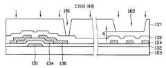
도 3은 실링재(22)에 의해 액정패널이 실링되는 실링영역을 자세히 나타내는 단면으로, 도 3(a)는 평면도이고 도 3(b)는 도 1 및 도 3(a)의 A-A'선 단면도이다.3 is a cross-sectional view showing in detail a sealing area in which a liquid crystal panel is sealed by the sealing
도면에 도시된 바와 같이, 게이트절연층(32) 위에 형성된 복수의 금속배선(24) 사이의 무기보호층(39)과 유기보호층(37)에는 개구(62)가 형성되어 있으며, 상기 실링영역(7)에 실링재(22)가 도포되는 경우 상기 개구(62)내에 실링재(22)가 충진되다. 상기와 같이 금속배선(24) 사이에 개구(62)를 형성하는 것은 다음과 같은 이유 때문이다.As shown in the drawing, an
상기 개구(62)가 형성되어 있지 않다고 가정하면, 유기보호층(37)이 형성된 액정표시소자에서는 액정패널을 합착, 실링하는 실링재(22)가 상기 유기보호층(37) 위에 직접 도포된다. 그런데, 포토아크릴이나 BCB 등의 유기물질과 실링재는 상호 부착력이 약하다는 것이 알려져 있다. 따라서, 상기 유기보호층(37)에 실링재(22)를 도포하여 액정패널을 합착하는 경우 약한 부착력에 의해 실링이 터지게 되어, 결국 액정패널에 주입된 액정이 외부로 누설되는 문제가 발생하게 된다. 반면에 SiNx와 같은 무기물질과 실링재 사이의 부착력은 상대적으로 양호하다고 알려져 있다. 따라서, 금속배선(24) 사이의 무기보호층(39)과 유기보호층(37)에 개구(62)를 형성하여 무기물질로 이루어진 게이트절연층(32)을 외부로 노출시킨 후 이 게이트절연층(32) 위에 실링재(22)를 충진하여 실링재(22)의 일부를 게이트절연층(32)에 직접 부착함으로서 액정패널의 합착력 강화를 도모한 것이다.Assuming that the
상기 실링영역(7)의 개구(62)는 도 2에 도시된 화소영역의 컨택홀(61)을 형성할 때 동시에 형성된다.The
그런데, 상기와 같이 금속배선(24) 사이의 무기보호층(39)과 유기보호층(37)에 개구(62)를 형성하여 액정패널의 접착력을 향상시키는 경우에도 문제는 발생한다. 일반적으로 실링재(22)에는 액정패널의 셀간격을 유지하기 위한 유리섬유(glass fiber)가 혼입되어 있다. 한편, 금속배선(24) 사이에 형성되는 개구(62)는 도면에 도시된 바와 같이 게이트절연층(32)쪽으로 갈수록 그 폭이 작아지게 되어 게이트절연층(32) 근방의 개구(62)의 폭은 매우 미세하게 된다. 이 미세한 개구(62)에 실링재(22)가 충진되는 경우 상기 유리섬유에 의해 상기 개구(62)가 막히게 되는데, 이 경우 충진되는 실링재(22)가 게이트절연층(32)까지 도달하지 않게 되어 실링재와 게이트절연층 사이의 접촉면적이 줄어 들게 되며, 그 결과 액정패널의 합착력이 오히려 저하되는 문제가 있었다.However, even when the
본 발명은 상기한 문제를 해결하기 위한 것으로, 액정표시소자의 실링영역에 형성된 유기보호층을 제거하여 실링재와 유기보호층 사이의 접촉면적을 최소화함과 동시에 실링재와 무기절연층 사이의 접촉면적을 최대화하여 패널의 접착력이 향상된 액정표시소자를 제공하는 것을 목적으로 한다.SUMMARY OF THE INVENTION The present invention has been made to solve the above-mentioned problem, and minimizes the contact area between the sealing material and the organic protective layer by removing the organic protective layer formed in the sealing region of the liquid crystal display device and at the same time reduces the contact area between the sealing material and the inorganic insulating layer. It is an object of the present invention to provide a liquid crystal display device in which the adhesion of the panel is maximized.
본 발명의 다른 목적은 절연층의 패터닝 공정을 2단계로 진행하여, 우선 화소영역의 무기절연층 패턴시 실링영역의 유기절연층의 일부를 제거한 후 화소영역의 유기절연층 패턴시 실링영역의 나머지 유기절연층을 제거하여 실링재가 충진되는 개구를 형성함으로써 패널의 합착력을 향상시킨 액정표시소자 제조방법을 제공하는 것이다.Another object of the present invention is to proceed with the patterning process of the insulating layer in two steps, first removing a part of the organic insulating layer of the sealing region when patterning the inorganic insulating layer of the pixel region, and then rest of the sealing region when patterning the organic insulating layer of the pixel region The present invention provides a method for manufacturing a liquid crystal display device in which the bonding force of the panel is improved by removing the organic insulating layer to form openings filled with the sealing material.
상기한 목적을 달성하기 위해, 본 발명에 따른 액정표시소자는 다수의 금속배선이 구비된 기판과, 상기 금속배선상에 형성된 제1절연층 및 제2절연층과, 상기 금속배선중 적어도 2개 이상에 걸쳐 상기 제2절연층에 형성된 실링용 홀과, 박막트랜지스터의 드레인전극이 노출되도록 제1절연층 및 제2절연층에 형성된 드레인컨택홀과, 상기 드레인컨택홀을 통해 드레인전극에 접속되는 화소전극과, 상기 실링용 홀에 형성된 실링재를 포함하여 구성된다.In order to achieve the above object, the liquid crystal display device according to the present invention is a substrate having a plurality of metal wiring, the first insulating layer and the second insulating layer formed on the metal wiring, and at least two of the metal wiring The sealing hole formed in the second insulating layer, the drain contact hole formed in the first insulating layer and the second insulating layer so as to expose the drain electrode of the thin film transistor, and the drain electrode are connected to the drain electrode through the drain contact hole. The pixel electrode and the sealing material formed in the said sealing hole are comprised.
상기 실링영역의 게이트절연층 위에는 박막트랜지스터의 화소전극시 형성된 금속배선이 복수개 형성되어 있으며, 상기 유기보호층은 포토아크릴 및 BCB(Benzocyclobutene)로 이루어진다.A plurality of metal wires formed at the pixel electrode of the thin film transistor are formed on the gate insulating layer of the sealing region, and the organic protective layer is made of photoacryl and BCB (benzoicbutene).
또한, 본 발명에 따른 액정표시소자 제조방법은 화소영역과 실링영역으로 이루어진 기판의 화소영역에 박막트랜지스터를 형성하고 기판 전체에 걸쳐서 무기층과 유기층을 형성하는 단계와, 상기 기판 위에 투과부가 박막트랜지스터에 정렬되고 회절부가 실링영역에 정렬된 회절마스크를 위치시킨 상태에서 광을 조사하여 유기층을 제거하는 단계와, 화소영역의 무기층을 제거하고 실링영역의 유기층을 제거하는 단계와, 화소영역의 유기보호층 위에 화소전극을 형성한 후 실링영역에 실링재를 도포하는 단계로 구성된다.In addition, the liquid crystal display device manufacturing method according to the present invention comprises the steps of forming a thin film transistor in the pixel region of the substrate consisting of a pixel region and a sealing region, and forming an inorganic layer and an organic layer over the entire substrate, the transmission portion on the substrate thin film transistor Irradiating light with the diffraction mask aligned with the diffraction portion aligned with the sealing region to remove the organic layer, removing the inorganic layer of the pixel region, and removing the organic layer of the sealing region, After forming the pixel electrode on the protective layer and applying a sealing material to the sealing region.
본 발명에서는 유기보호층이 형성된 액정패널의 합착력을 강화시키기 위해, 실링영역의 유기보호층을 제거하여 실링재와 유기보호층 사이의 접촉면적을 최소화하고 실링재와 무기보호층 사이의 접촉면적을 최대화한다. 유기보호층으로는 포토아크릴이나 BCB를 사용한다.In the present invention, in order to enhance the bonding strength of the liquid crystal panel formed with an organic protective layer, the organic protective layer of the sealing region is removed to minimize the contact area between the sealing material and the organic protective layer and maximize the contact area between the sealing material and the inorganic protective layer. do. Photoacryl or BCB is used as an organic protective layer.
무기보호층만이 형성되어 있던 종래의 액정표시소자에서는 화소전극이 상기 무기보호층 위에 형성되어 있기 때문에, 게이트라인(외부로부터의 주사신호를 게이트전극에 인가하는)과 화소전극 사이 및 데이터라인(외부로부터의 화상신호를 소스/드레인전극을 통해 화소전극에 인가하는)과 화소전극 사이에 일정한 간격을 유지하고 있어야만 한다. 만약, 상기 게이트라인이나 데이터라인이 보호층을 사이에 두고 화소전극의 일부와 겹치는 경우, 기생용량이 발생하게 되어 수직 크로스토 크(crosstalk)가 발생하게 된다. 이 크로스토크는 플리커(flicker)현상을 야기하게 되어 액정표시장치의 화질을 저하시키는 주요한 요인이 된다.In the conventional liquid crystal display device in which only the inorganic protective layer is formed, since the pixel electrode is formed on the inorganic protective layer, the gate line (applying a scan signal from the outside to the gate electrode) and the pixel electrode and the data line (external Must be maintained at a constant distance between the pixel electrode) and the image signal from the pixel electrode. If the gate line or the data line overlaps a part of the pixel electrode with a protective layer interposed therebetween, parasitic capacitance is generated and vertical crosstalk is generated. This crosstalk causes flicker, which is a major factor in degrading the image quality of the liquid crystal display.
반면에 유기보호층이 구비된 액정표시소자에서는 저유전상수의 유기물을 보호층으로 적층하기 때문에, 게이트라인이나 데이터라인이 화소전극과 겹치는 경우에도 기생용량이 거의 발생하지 않게 된다. 다시 말해서, 상기 유기보호층이 구비된 액정표시소자에서는 화소전극을 게이트라인이나 데이터라인과 겹치게 배치할 수 있기 때문에, 무기보호층이 형성된 액정표시소자에 비해 고개구율을 갖는 액정표시장치를 제작할 수 있게 된다. 또한, 이러한 유기보호층이 구비된 액정표시소자에서는 유기물질의 특성상 평탄한 표면을 갖는 층을 형성할 수 있다는 장점도 가진다.On the other hand, in the liquid crystal display device having the organic protective layer, since the organic material having the low dielectric constant is stacked as the protective layer, parasitic capacitance hardly occurs even when the gate line or the data line overlaps the pixel electrode. In other words, in the liquid crystal display device having the organic protective layer, since the pixel electrode may be disposed to overlap the gate line or the data line, the liquid crystal display device having a higher opening ratio may be manufactured than the liquid crystal display device having the inorganic protective layer. Will be. In addition, the liquid crystal display device having the organic protective layer also has an advantage of forming a layer having a flat surface in view of the characteristics of the organic material.
본 발명에서는 이러한 유기보호층을 구비한 액정표시소자의 실링영역에 형성된 유기보호층을 제거해서 실링재가 충진되는 개구를 형성하여 실링재와 무기보호층 사이의 접촉면적을 증가시킴으로써 액정패널의 합착력을 향상시킨다. 특히, 종래의 액정표시소자에서는 실링영역의 금속배선 사이의 유기보호층과 무기보호층을 제거하여 금속배선 사이에만 개구를 형성하는데 비해, 본 발명에서는 적어도 2개의 금속배선에 걸쳐 형성된 유기보호층, 바람직하게는 실링영역 전체의 유기보호층을 제거하여 더 넓은 개구를 형성하므로 더욱 효과적인 합착력 향상효과를 얻을 수 있게 된다.In the present invention, the organic protective layer formed in the sealing area of the liquid crystal display device having the organic protective layer is removed to form an opening filled with the sealing material, thereby increasing the contact area between the sealing material and the inorganic protective layer, thereby increasing the bonding strength of the liquid crystal panel. Improve. In particular, the conventional liquid crystal display device removes the organic protective layer and the inorganic protective layer between the metal wiring of the sealing region to form an opening only between the metal wiring, in the present invention, the organic protective layer formed over at least two metal wiring, Preferably, since the organic protective layer of the entire sealing region is removed to form a wider opening, a more effective adhesion improvement effect can be obtained.
상기와 같이, 종래에 실링영역의 금속배선 사이에만 개구를 형성하는 이유는 개구형성공정(즉, 보호층 패터닝공정)이 박막트랜지스터의 컨택홀 공정과 동시에 진행되기 때문이다. 즉, 박막트랜지스터의 컨택홀을 형성하기 위해서는 유기보호층과 무기보호층을 패터닝해야만 하므로, 실링영역에서도 이와 같이 유기보호층과 무기보호층이 패터닝된다. 그런데, 무기보호층이 패터닝되는 경우 실링영역의 개구에는 금속배선이 외부로 노출되어 실링재가 직접 상기 금속배선에 접촉하게 되는데, 실링재와 금속배선 사이의 나쁜 계면특성에 의해 접착력이 저하될 뿐만 아니라 소자특성에도 나쁜 영향을 미치게 된다.As described above, the reason why the opening is formed only between the metal wirings of the sealing region in the related art is that the opening forming process (ie, the protective layer patterning process) proceeds simultaneously with the contact hole process of the thin film transistor. That is, since the organic protective layer and the inorganic protective layer must be patterned in order to form the contact hole of the thin film transistor, the organic protective layer and the inorganic protective layer are also patterned in the sealing region. However, when the inorganic protective layer is patterned, the metal wiring is exposed to the outside of the opening of the sealing region so that the sealing material directly contacts the metal wiring, and the adhesive force is deteriorated due to the bad interface property between the sealing material and the metal wiring. It will also have a bad effect on the quality.
본 발명에서는 상기한 점을 감안하여 새로운 방법에 의해 실링영역에 개구를 형성한다. 물론 본 발명에서도 박막트랜지스터의 컨택홀 형성공정과 동시에 실링영역의 개구를 형성하지만, 컨택홀에는 유기보호층과 무기보호층이 모두 제거되는 반면에 실링영역에서는 단지 유기보호층만이 제거된다. 즉, 보호층의 패턴공정을 2단계로 나누어 제1단계에서는 박막트랜지스터에서 컨택홀을 형성하기 위해 유기보호층을 완전히 제거함과 동시에 실링영역에서는 유기보호층의 일부만을 제거하여 소정 두께의 유기보호층이 남아 있도록 하며, 제2단계에서는 박막트랜지스터의 무기보호층을 제거할 때 실링영역의 나머지 유기보호층을 제거함으로써 결국 실링영역의 개구에 무기보호층만을 노출시킬 수 있게 된다. 이때, 상기 무기보호층의 일부가 제거되는 경우에도 상기 실링재가 무기보호층에 직접 접촉하기 때문에, 무기보호층의 일부를 에칭할 수도 있다.In view of the above, the present invention forms an opening in the sealing region by a new method. Of course, in the present invention, the opening of the sealing region is formed at the same time as the contact hole forming process of the thin film transistor, but both the organic protective layer and the inorganic protective layer are removed from the contact hole, whereas only the organic protective layer is removed from the sealing region. That is, the patterning process of the protective layer is divided into two steps. In the first step, the organic protective layer is completely removed to form contact holes in the thin film transistor, and only a part of the organic protective layer is removed in the sealing region. In the second step, when the inorganic protective layer of the thin film transistor is removed, the remaining organic protective layer of the sealing region is removed, so that only the inorganic protective layer can be exposed to the opening of the sealing region. At this time, even when a part of the inorganic protective layer is removed, since the sealing material directly contacts the inorganic protective layer, a part of the inorganic protective layer may be etched.
이하, 첨부한 도면을 참조하여 본 발명에 따른 액정표시소자 및 그 제조방법을 더욱 상세히 설명한다.Hereinafter, a liquid crystal display device and a method of manufacturing the same according to the present invention will be described in detail with reference to the accompanying drawings.
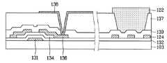
도 4에 본 발명에 따른 액정표시소자의 실링영역의 구조가 도시되어 있다. 도면에 도시된 바와 같이, 유리와 같은 투명한 기판(103) 상에는 절연층(132)이 적층되어 있으며, 그 위에 금속배선(124)이 형성되어 있다. 이 금속배선(124)은 데이터라인 또는 게이트라인이 연장되어 외부 접속용 패드에 연결된 것으로, 게이트라인이 연장된 경우에는 상기 금속배선(124)은 기판(103) 위에 형성된다. 상기 금속배선(124) 위에는 무기물질로 이루어진 무기보호층(139)이 형성되어 있고 그 위에 개구(162)가 형성된 유기보호층(137)이 형성되어 있다. 도면에 도시된 바와 같이, 상기 개구(162)는 적어도 2개의 금속배선(124)을 걸쳐, 바람직하게는 실링영역의 거의 전체에 걸쳐 형성되어, 상대적으로 넓은 면적의 무기보호층(139)이 외부로 노출된다. 상기 유기보호층(139) 위 및 개구(162)에는 실링재(122)가 도포되어 있다.4 illustrates a structure of a sealing region of the liquid crystal display device according to the present invention. As shown in the figure, an insulating
상기와 같이, 본 발명에서는 실링재(122)가 넓은 영역의 개구(162)에 충진되어 무기보호층(139)과 직접 접촉하는 면적을 최대로 하고 유기보호층(137)과 접촉하는 면적은 최소로 하기 때문에 접착력이 향상된다. 더욱이 상기 개구(162)의 폭은 실링재(122)에 포함되는 유리섬유보다는 훨씬 크기 때문에 유리섬유에 의해 개구가 막히는 현상을 방지할 수 있게 된다.As described above, in the present invention, the sealing
상기한 구조의 액정표시소자에서 금속층(124)은 박막트랜지스터의 소스/드레인전극(또는 데이터라인)과 동시에 형성되며, 개구는 박막트랜지스터의 컨택홀 형성과 동시에 이루어진다. 이하에서는 이러한 본 발명에 따른 액정표시소자의 제조방법을 구체적으로 설명한다.In the liquid crystal display device having the above structure, the
도 5는 본 발명에 따른 액정표시소자 제조방법을 나타내는 도면이다. 도면에서는 설명의 편의를 위해, 박막트랜지스터가 형성되는 화소영역과 실링영역로 구분하였으며, 상기 실링영역은 도 1의 A-A'선을 따라 절취된 단면으로 설명한다.5 is a view showing a method for manufacturing a liquid crystal display device according to the present invention. In the drawing, for convenience of description, the thin film transistor is divided into a pixel region and a sealing region, and the sealing region is described as a cross section taken along the line AA ′ of FIG. 1.
도 5(a)에 도시된 바와 같이, 우선 투명한 유리기판(103)상에 게이트전극(131)을 형성한 후 기판(103) 전체에 걸쳐서 게이트절연층(132)을 적층한다. 이어서, 화소영역의 게이트절연층(132) 위에 반도체층(134)을 형성하고 그 위에 소스/드레인전극(136)을 형성한다. 한편, 상기 소스/드레인전극(136)의 형성과 동시에 실링영역에는 복수의 금속층(124)이 형성된다. 이때 상기 금속층(124)을 게이트전극(131)과 동시에 기판(103)위에 형성할 수도 있다. 이후, 상기 기판(103) 전체에 걸쳐서 SiNx와 같은 무기물질을 적층하여 무기보호층(139)을 형성한 후 계속하여 포토아크릴이나 BCB와 같은 유기물질을 도포하여 유기보호층(137)을 형성한다.As shown in FIG. 5A, first, the
상기와 같이 박막트랜지스터가 형성된 기판(103)의 상부에 마스크(도면표시하지 않음)를 위치시킨 후 자외선과 같은 광을 조사한다. 상기 마스크는 회절마스크로서,도면에 도시된 바와 같이 조사되는 광을 차단하는 차단부와, 광을 투과시키는 투과부와, 복수의 슬릿으로 이루어져 조사되는 광을 회절시키는 회절부로 구성되어 있다. 투과부는 박막트랜지스터의 소스/드레인전극(136) 위에 위치하며 회절부는 실링영역에 위치한다. 회절부에서는 복수의 슬릿에 의해 광이 회절되어 투과부보다 작은 세기의 광이 실링영역의 유기보호층에 조사된다. 이때, 회절부에 의해 회절되는 광의 세기는 슬릿의 갯수 또는 슬릿의 간격에 따라 조절할 수 있다.As described above, after placing a mask (not shown) on the
상기와 같이 광이 조사된 유기보호층(137)에 현상액을 작용하면, 도 5(b)에 도시된 바와 같이 마스크(170)의 투과부(170b)에 해당하는 영역인 소스/드레인전극 위의 컨택홀 형성영역의 유기보호층(137)은 완전히 제거되어 무기보호층(139)이 외 부로 노출되는 반면에 회절부(170c)에 해당하는 영역인 실링영역의 유기보호층(137)은 그 일부만이 제거되어 무기보호층(139) 위에 일정 두께(a)의 유기보호층(137)이 남아 있게 된다.When the developer is applied to the organic
이후, 에천트가스를 이용한 드라이에칭에 의해 도 5(c)에 도시된 바와 같이 화소영역의 노출된 무기보호층(139)과 실링영역에 남아 있는 유기보호층(137)을 에칭하여 상기 소스/드레인전극(136) 위에 컨택홀(161)을 형성함과 동시에 실링영역의 유기보호층(137)에 개구(162)를 형성한다. 상기한 공정에 의해 컨택홀(161)의 하부에는 소스/드레인전극(136)이 외부로 노출되고 실링영역에서는 무기보호층(139)이 외부로 노출된다.Thereafter, as shown in FIG. 5 (c) by dry etching using an etchant gas, the exposed inorganic
이어서, 화소영역에 ITO와 같은 투명한 금속을 적층하여 컨택홀(161)을 통해 소스/드레인전극(136)과 접속되는 화소전극(138)을 형성하고 도면표시하지 않은 배향막을 형성한 후 도 5(d)에 도시된 바와 같이 실링영역에 실링재(122)를 도포한다. 이때, 실링영역에 도포된 실링재(122)는 무기보호층(139) 위에 형성된 개구(162)에 충진되어 무기보호층(139)에 직접 접촉하게 되며 유기보호층(137)과는 최소한의 면적만이 접촉하므로 실링재의 합착력이 저하되지 않는다. 상기와 같이 형성된 기판에 컬러필터가 형성된 기판을 위치시킨 상태에서 압력을 가하면 실링재에 의해 기판이 실링되어 액정표시소자가 완성된다.Subsequently, a transparent metal such as ITO is stacked on the pixel region to form a
상기한 바와 같이, 본 발명에서는 액정표시소자의 실링영역의 유기보호층을 대부분 제거하여 유기보호층과 실링재의 접착력 저하에 의해 액정패널의 실링이 파손되는 것을 방지한다. 이것을 위해, 본 발명에서는 회절마스크를 이용하여 박막트 랜지스트의 컨택홀 형성시 유기보호층만을 제거하였다. 이러한 본 발명은 어떠한 구조의 액정표시소자에도 적용될 수 있다. 기본적으로 액정표시소자는 구동소자가 형성된 제1기판과 컬러필터가 형성된 제2기판으로 구성되며, 이 제1기판 및 제2기판이 실링재에 의해 합착되고 그 사이에 액정이 주입됨으로써 완성되기 때문에, 실링영역의 실링재와 상기 실링재가 도포되는 층 사이의 합착력은 모든 종류의 액정표시소자에서 중요한 문제가 되고 있다. 본 발명은 이러한 문제를 해결한 것으로써, 모든 종류의 액정표시소자에 적용될 수 있을 것이다.As described above, in the present invention, most of the organic protective layer of the sealing region of the liquid crystal display device is removed to prevent the sealing of the liquid crystal panel from being damaged by the deterioration of the adhesive force between the organic protective layer and the sealing material. To this end, in the present invention, only the organic protective layer is removed when forming the contact hole of the thin film transistor using a diffraction mask. This invention can be applied to the liquid crystal display device of any structure. Basically, the liquid crystal display device is composed of a first substrate on which a driving element is formed and a second substrate on which a color filter is formed, and since the first and second substrates are joined by a sealing material and liquid crystal is injected therebetween, Bonding force between the sealing material of the sealing region and the layer on which the sealing material is applied is an important problem in all kinds of liquid crystal display devices. The present invention solves this problem, and can be applied to all kinds of liquid crystal display devices.
이러한 본 발명을 이용한 다른 실시예나 변형례는 본 발명의 기술분야에 속하는 사람에게는 자명한 것으로, 당연히 본 발명의 권리범위에 속해야만 할 것이다.Other embodiments or modifications using the present invention will be apparent to those of ordinary skill in the art and should naturally fall within the scope of the present invention.
본 발명은 상술한 바와 같이, 액정표시소자의 실링영역에 형성된 유기보호층을 회절마스크를 이용하여 박막트랜지스터의 컨택홀 형성시 2단계의 공정에 의해 제거한다. 따라서, 실링영역에 도포되는 실링재가 최대한의 넓은 면적으로 무기보호층에 접촉하고 유기보호층과는 최소한의 면적만이 접촉하므로 유기보호층과 실링재의 접착불량에 의한 액정패널의 접착력을 저하를 방지할 수 있게 된다. 이때, 유기보호층 하부에 형성되는 무기보호층은 제거되지 않게 되기 때문에, 상기 실링재가 금속배선과는 접촉하지 않게 되므로 더욱 향상된 접착력을 얻을 수 있게 된다.As described above, the organic protective layer formed in the sealing region of the liquid crystal display device is removed by a two-step process in forming the contact hole of the thin film transistor using a diffraction mask. Therefore, since the sealing material applied to the sealing area is in contact with the inorganic protective layer with the largest area and only the minimum area is in contact with the organic protective layer, the adhesive force of the liquid crystal panel is prevented from being lowered due to the poor adhesion between the organic protective layer and the sealing material. You can do it. In this case, since the inorganic protective layer formed under the organic protective layer is not removed, the sealing material does not come into contact with the metal wiring, and thus, more improved adhesion may be obtained.
Claims (9)
Translated fromKoreanPriority Applications (3)
| Application Number | Priority Date | Filing Date | Title |
|---|---|---|---|
| KR1020010089306AKR100870660B1 (en) | 2001-12-31 | 2001-12-31 | Liquid crystal display device and manufacturing method with improved adhesion of panel |
| US10/314,373US6859254B2 (en) | 2001-12-31 | 2002-12-09 | Liquid crystal display device and method for fabricating the same |
| US10/929,544US20050024581A1 (en) | 2001-12-31 | 2004-08-31 | Liquid crystal display device and method for fabricating the same |
Applications Claiming Priority (1)
| Application Number | Priority Date | Filing Date | Title |
|---|---|---|---|
| KR1020010089306AKR100870660B1 (en) | 2001-12-31 | 2001-12-31 | Liquid crystal display device and manufacturing method with improved adhesion of panel |
Publications (2)
| Publication Number | Publication Date |
|---|---|
| KR20030058772A KR20030058772A (en) | 2003-07-07 |
| KR100870660B1true KR100870660B1 (en) | 2008-11-26 |
Family
ID=19718039
Family Applications (1)
| Application Number | Title | Priority Date | Filing Date |
|---|---|---|---|
| KR1020010089306AExpired - Fee RelatedKR100870660B1 (en) | 2001-12-31 | 2001-12-31 | Liquid crystal display device and manufacturing method with improved adhesion of panel |
Country Status (2)
| Country | Link |
|---|---|
| US (2) | US6859254B2 (en) |
| KR (1) | KR100870660B1 (en) |
Families Citing this family (33)
| Publication number | Priority date | Publication date | Assignee | Title |
|---|---|---|---|---|
| JP2003347044A (en)* | 2002-05-30 | 2003-12-05 | Sanyo Electric Co Ltd | Organic el panel |
| TWI325983B (en)* | 2002-10-25 | 2010-06-11 | Au Optronics Corp | Liquid crystal displays |
| KR20040061292A (en)* | 2002-12-30 | 2004-07-07 | 엘지.필립스 엘시디 주식회사 | A method of fabricating liquid crystal display device |
| KR100972148B1 (en) | 2002-12-31 | 2010-07-23 | 엘지디스플레이 주식회사 | Liquid crystal display device characterized by the laminated structure under the seal pattern |
| EP1611636B1 (en)* | 2003-04-04 | 2008-12-03 | Hannah B. Zweidorff | A device for shielding electronic units including a transmitting/receiving equipment and especially for shielding mobile phones |
| KR100965139B1 (en)* | 2003-07-25 | 2010-06-23 | 삼성전자주식회사 | Array substrate, method for manufacturing same, liquid crystal display including the array substrate and method for manufacturing same |
| CN100357813C (en)* | 2003-10-22 | 2007-12-26 | 友达光电股份有限公司 | Display panel frame glue structure |
| KR101010113B1 (en)* | 2003-12-30 | 2011-01-24 | 엘지디스플레이 주식회사 | Transverse electric field mode liquid crystal display device with stable common voltage |
| KR101158903B1 (en)* | 2005-08-05 | 2012-06-25 | 삼성전자주식회사 | Substrate For Display Device, Method of Manufacturing The Same, And Display Device Having The Same |
| KR101272488B1 (en)* | 2005-10-18 | 2013-06-07 | 삼성디스플레이 주식회사 | Thin Transistor Substrate, Method Of Fabricating The Same, Liquid Crystal Display Having The Same And Method Of Fabricating Liquid Crystal Display Having The Same |
| EP1798237A1 (en)* | 2005-12-16 | 2007-06-20 | Pharmatex Italia Srl | Process for the purification of macrolide antibiotics |
| KR100702032B1 (en)* | 2006-03-07 | 2007-03-30 | 삼성전자주식회사 | High density probe array, storage device having the probe array and methods of manufacturing the same |
| KR101244898B1 (en) | 2006-06-28 | 2013-03-19 | 삼성디스플레이 주식회사 | Organic Thin Film Transistor Substrate And Fabricating Method Thereof |
| JP5178327B2 (en)* | 2007-08-22 | 2013-04-10 | 株式会社ジャパンディスプレイウェスト | LIQUID CRYSTAL DISPLAY PANEL, ELECTRONIC DEVICE HAVING LIQUID CRYSTAL DISPLAY PANEL, AND METHOD FOR PRODUCING LIQUID CRYSTAL DISPLAY |
| US8125602B2 (en)* | 2007-08-22 | 2012-02-28 | Sony Corporation | Liquid crystal display panel, electronic apparatus equipped with the same, and method for manufacturing liquid crystal display panel |
| KR20090100056A (en)* | 2008-03-19 | 2009-09-23 | 삼성전자주식회사 | Liquid Crystal Display and Manufacturing Method Thereof |
| KR100995071B1 (en)* | 2008-09-12 | 2010-11-18 | 삼성모바일디스플레이주식회사 | Organic light emitting display |
| CN101713882B (en)* | 2008-10-01 | 2013-07-17 | 株式会社日立显示器 | Liquid crystal display device |
| TWI406064B (en)* | 2010-12-31 | 2013-08-21 | Au Optronics Corp | Display panel |
| US20130135549A1 (en)* | 2011-11-29 | 2013-05-30 | Songxian Wen | Thin film transistor array substrate and liquid crystal display device and method for manufacturing the same |
| US20130308082A1 (en)* | 2012-05-17 | 2013-11-21 | Shenzhen China Star Optoelectronics Technology Co., Ltd. | Liquid Crystal Display Panel |
| KR102049732B1 (en)* | 2012-07-16 | 2019-11-29 | 엘지디스플레이 주식회사 | Liquid crystal display device |
| KR102117109B1 (en) | 2013-10-22 | 2020-06-01 | 삼성디스플레이 주식회사 | Organic light-emitting display apparatus |
| KR102118676B1 (en) | 2014-02-05 | 2020-06-04 | 삼성디스플레이 주식회사 | Organic light-emitting display apparatus |
| KR102205402B1 (en) | 2014-02-05 | 2021-01-21 | 삼성디스플레이 주식회사 | Organic light-emitting display apparatus |
| KR102430578B1 (en)* | 2015-11-30 | 2022-08-09 | 엘지디스플레이 주식회사 | Display Device and Method of Manufacturing the same |
| KR102375975B1 (en)* | 2017-04-28 | 2022-03-17 | 삼성디스플레이 주식회사 | Display device, organic light emitting display device and head mount display device |
| US10690787B2 (en) | 2018-07-16 | 2020-06-23 | Vieworks Co., Ltd. | Radiation imaging system |
| US10466370B1 (en)* | 2018-07-16 | 2019-11-05 | Vieworks Co., Ltd. | Radiation imaging system |
| CN111463220B (en)* | 2020-04-09 | 2022-11-25 | 深圳市华星光电半导体显示技术有限公司 | Array substrate and display device |
| TWI752508B (en)* | 2020-05-26 | 2022-01-11 | 群創光電股份有限公司 | Display device |
| CN113867053B (en)* | 2020-06-30 | 2023-05-16 | 京东方科技集团股份有限公司 | Display panel and preparation method thereof |
| CN113867025B (en) | 2021-09-23 | 2024-01-23 | 武汉华星光电技术有限公司 | Display panel and mobile terminal |
Citations (3)
| Publication number | Priority date | Publication date | Assignee | Title |
|---|---|---|---|---|
| JPH0933933A (en)* | 1995-07-24 | 1997-02-07 | Fujitsu Ltd | LCD display panel |
| KR19980080828A (en)* | 1997-03-27 | 1998-11-25 | 니시무로다이조 | LCD and its manufacturing method |
| KR20010105058A (en)* | 2000-05-18 | 2001-11-28 | 구본준, 론 위라하디락사 | Method for fabricating the array substrate for LCD and the same |
Family Cites Families (12)
| Publication number | Priority date | Publication date | Assignee | Title |
|---|---|---|---|---|
| JP2991407B2 (en)* | 1995-02-24 | 1999-12-20 | 日本電気株式会社 | Liquid crystal display device and method of manufacturing the same |
| US6372534B1 (en)* | 1995-06-06 | 2002-04-16 | Lg. Philips Lcd Co., Ltd | Method of making a TFT array with photo-imageable insulating layer over address lines |
| JP3299869B2 (en)* | 1995-09-27 | 2002-07-08 | シャープ株式会社 | Liquid crystal display device and manufacturing method thereof |
| US5953094A (en)* | 1997-04-04 | 1999-09-14 | Sanyo Electric Co., Ltd. | Liquid crystal display device |
| US6271907B1 (en)* | 1997-09-14 | 2001-08-07 | Canon Kabushiki Kaisha | Color liquid crystal device having injection port parallel to the stripe electrodes on the substrate with color filter and flattening film and the other substrate free from color filter and flattening film protruded |
| KR100293980B1 (en)* | 1997-12-31 | 2001-07-12 | 윤종용 | Liquid crystal display with drive circuits separated from the pixel area by the room |
| KR100379287B1 (en)* | 1999-06-25 | 2003-04-10 | 닛뽄덴끼 가부시끼가이샤 | Multi domain LCD device |
| KR100315208B1 (en)* | 1999-12-17 | 2001-11-26 | 구본준, 론 위라하디락사 | Liquid Crystal Display Device and Method of Fabricating the Same |
| JP2001312214A (en)* | 2000-04-27 | 2001-11-09 | Seiko Epson Corp | Manufacturing method of electro-optical device, pressure-sensitive adhesive curing device, electro-optical device, and electronic apparatus |
| JP4609679B2 (en)* | 2000-07-19 | 2011-01-12 | 日本電気株式会社 | Liquid crystal display |
| KR100466627B1 (en)* | 2001-02-27 | 2005-01-15 | 삼성에스디아이 주식회사 | Multi display device |
| KR100737895B1 (en)* | 2002-09-18 | 2007-07-10 | 삼성전자주식회사 | Reflective and reflective-transmissive liquid crystal display and manufacturing method thereof |
- 2001
- 2001-12-31KRKR1020010089306Apatent/KR100870660B1/ennot_activeExpired - Fee Related
- 2002
- 2002-12-09USUS10/314,373patent/US6859254B2/ennot_activeExpired - Lifetime
- 2004
- 2004-08-31USUS10/929,544patent/US20050024581A1/ennot_activeAbandoned
Patent Citations (3)
| Publication number | Priority date | Publication date | Assignee | Title |
|---|---|---|---|---|
| JPH0933933A (en)* | 1995-07-24 | 1997-02-07 | Fujitsu Ltd | LCD display panel |
| KR19980080828A (en)* | 1997-03-27 | 1998-11-25 | 니시무로다이조 | LCD and its manufacturing method |
| KR20010105058A (en)* | 2000-05-18 | 2001-11-28 | 구본준, 론 위라하디락사 | Method for fabricating the array substrate for LCD and the same |
Also Published As
| Publication number | Publication date |
|---|---|
| US20050024581A1 (en) | 2005-02-03 |
| US20030122983A1 (en) | 2003-07-03 |
| US6859254B2 (en) | 2005-02-22 |
| KR20030058772A (en) | 2003-07-07 |
Similar Documents
| Publication | Publication Date | Title |
|---|---|---|
| KR100870660B1 (en) | Liquid crystal display device and manufacturing method with improved adhesion of panel | |
| US20220308375A1 (en) | Liquid crystal display device | |
| US8284376B2 (en) | Method for manufacturing color filter on thin film transistor (COT) type liquid crystal display device having black matrix in region outside of pixel region | |
| US8068205B2 (en) | Method of fabricating a liquid crystal display device using gate and common links to link gate and common lines to gate and common pads | |
| US7446826B2 (en) | Display panel and method of manufacture | |
| KR20040042411A (en) | a panel for a liquid crystal display | |
| JP2004118200A (en) | Display panel for liquid crystal display device, method of manufacturing the same, and liquid crystal display device using the same | |
| JP2011017834A (en) | Liquid crystal display device | |
| KR20120014507A (en) | Liquid crystal display | |
| KR20060115464A (en) | LCD and its manufacturing method | |
| KR20080050822A (en) | LCD Display | |
| US6897099B2 (en) | Method for fabricating liquid crystal display panel | |
| KR100790352B1 (en) | Reflective and transflective liquid crystal display devices and manufacturing methods thereof | |
| JP2008139555A (en) | Liquid crystal display device and manufacturing method thereof | |
| US6967703B2 (en) | Liquid crystal display device and method thereof | |
| KR20040061292A (en) | A method of fabricating liquid crystal display device | |
| KR100656919B1 (en) | Liquid crystal display substrate and its manufacturing method | |
| JP3648337B2 (en) | Active matrix liquid crystal display device | |
| KR101366537B1 (en) | Array substrate in liquid crystal display device and Method for fabricating the same | |
| KR20050000447A (en) | liquid crystal display devices | |
| KR101097128B1 (en) | Method of fabricating the liquid crystal display device | |
| KR101096715B1 (en) | Liquid Crystal Display Device | |
| JP2001021915A (en) | Cf-on tft panel and production thereof | |
| KR20070008854A (en) | Liquid crystal display device and manufacturing method thereof | |
| KR20060134504A (en) | Display panel and display device having same |
Legal Events
| Date | Code | Title | Description |
|---|---|---|---|
| PA0109 | Patent application | St.27 status event code:A-0-1-A10-A12-nap-PA0109 | |
| PG1501 | Laying open of application | St.27 status event code:A-1-1-Q10-Q12-nap-PG1501 | |
| A201 | Request for examination | ||
| P11-X000 | Amendment of application requested | St.27 status event code:A-2-2-P10-P11-nap-X000 | |
| P13-X000 | Application amended | St.27 status event code:A-2-2-P10-P13-nap-X000 | |
| PA0201 | Request for examination | St.27 status event code:A-1-2-D10-D11-exm-PA0201 | |
| D13-X000 | Search requested | St.27 status event code:A-1-2-D10-D13-srh-X000 | |
| D14-X000 | Search report completed | St.27 status event code:A-1-2-D10-D14-srh-X000 | |
| E902 | Notification of reason for refusal | ||
| PE0902 | Notice of grounds for rejection | St.27 status event code:A-1-2-D10-D21-exm-PE0902 | |
| P11-X000 | Amendment of application requested | St.27 status event code:A-2-2-P10-P11-nap-X000 | |
| P13-X000 | Application amended | St.27 status event code:A-2-2-P10-P13-nap-X000 | |
| PN2301 | Change of applicant | St.27 status event code:A-3-3-R10-R13-asn-PN2301 St.27 status event code:A-3-3-R10-R11-asn-PN2301 | |
| E902 | Notification of reason for refusal | ||
| PE0902 | Notice of grounds for rejection | St.27 status event code:A-1-2-D10-D21-exm-PE0902 | |
| P11-X000 | Amendment of application requested | St.27 status event code:A-2-2-P10-P11-nap-X000 | |
| P13-X000 | Application amended | St.27 status event code:A-2-2-P10-P13-nap-X000 | |
| E701 | Decision to grant or registration of patent right | ||
| PE0701 | Decision of registration | St.27 status event code:A-1-2-D10-D22-exm-PE0701 | |
| GRNT | Written decision to grant | ||
| PR0701 | Registration of establishment | St.27 status event code:A-2-4-F10-F11-exm-PR0701 | |
| PR1002 | Payment of registration fee | St.27 status event code:A-2-2-U10-U11-oth-PR1002 Fee payment year number:1 | |
| PG1601 | Publication of registration | St.27 status event code:A-4-4-Q10-Q13-nap-PG1601 | |
| R18-X000 | Changes to party contact information recorded | St.27 status event code:A-5-5-R10-R18-oth-X000 | |
| PR1001 | Payment of annual fee | St.27 status event code:A-4-4-U10-U11-oth-PR1001 Fee payment year number:4 | |
| R18-X000 | Changes to party contact information recorded | St.27 status event code:A-5-5-R10-R18-oth-X000 | |
| R18-X000 | Changes to party contact information recorded | St.27 status event code:A-5-5-R10-R18-oth-X000 | |
| FPAY | Annual fee payment | Payment date:20120928 Year of fee payment:5 | |
| PR1001 | Payment of annual fee | St.27 status event code:A-4-4-U10-U11-oth-PR1001 Fee payment year number:5 | |
| FPAY | Annual fee payment | Payment date:20130930 Year of fee payment:6 | |
| PR1001 | Payment of annual fee | St.27 status event code:A-4-4-U10-U11-oth-PR1001 Fee payment year number:6 | |
| FPAY | Annual fee payment | Payment date:20141021 Year of fee payment:7 | |
| PR1001 | Payment of annual fee | St.27 status event code:A-4-4-U10-U11-oth-PR1001 Fee payment year number:7 | |
| FPAY | Annual fee payment | Payment date:20151028 Year of fee payment:8 | |
| PR1001 | Payment of annual fee | St.27 status event code:A-4-4-U10-U11-oth-PR1001 Fee payment year number:8 | |
| FPAY | Annual fee payment | Payment date:20161012 Year of fee payment:9 | |
| PR1001 | Payment of annual fee | St.27 status event code:A-4-4-U10-U11-oth-PR1001 Fee payment year number:9 | |
| FPAY | Annual fee payment | Payment date:20171016 Year of fee payment:10 | |
| PR1001 | Payment of annual fee | St.27 status event code:A-4-4-U10-U11-oth-PR1001 Fee payment year number:10 | |
| FPAY | Annual fee payment | Payment date:20181015 Year of fee payment:11 | |
| PR1001 | Payment of annual fee | St.27 status event code:A-4-4-U10-U11-oth-PR1001 Fee payment year number:11 | |
| FPAY | Annual fee payment | Payment date:20191015 Year of fee payment:12 | |
| PR1001 | Payment of annual fee | St.27 status event code:A-4-4-U10-U11-oth-PR1001 Fee payment year number:12 | |
| PC1903 | Unpaid annual fee | St.27 status event code:A-4-4-U10-U13-oth-PC1903 Not in force date:20201121 Payment event data comment text:Termination Category : DEFAULT_OF_REGISTRATION_FEE | |
| PC1903 | Unpaid annual fee | St.27 status event code:N-4-6-H10-H13-oth-PC1903 Ip right cessation event data comment text:Termination Category : DEFAULT_OF_REGISTRATION_FEE Not in force date:20201121 |