KR100870013B1 - Thin film transistor array substrate and manufacturing method thereof - Google Patents
Thin film transistor array substrate and manufacturing method thereofDownload PDFInfo
- Publication number
- KR100870013B1 KR100870013B1KR1020020050778AKR20020050778AKR100870013B1KR 100870013 B1KR100870013 B1KR 100870013B1KR 1020020050778 AKR1020020050778 AKR 1020020050778AKR 20020050778 AKR20020050778 AKR 20020050778AKR 100870013 B1KR100870013 B1KR 100870013B1
- Authority
- KR
- South Korea
- Prior art keywords
- gate
- line
- layer
- data
- electrode
- Prior art date
- Legal status (The legal status is an assumption and is not a legal conclusion. Google has not performed a legal analysis and makes no representation as to the accuracy of the status listed.)
- Expired - Fee Related
Links
Images


Classifications
- G—PHYSICS
- G02—OPTICS
- G02F—OPTICAL DEVICES OR ARRANGEMENTS FOR THE CONTROL OF LIGHT BY MODIFICATION OF THE OPTICAL PROPERTIES OF THE MEDIA OF THE ELEMENTS INVOLVED THEREIN; NON-LINEAR OPTICS; FREQUENCY-CHANGING OF LIGHT; OPTICAL LOGIC ELEMENTS; OPTICAL ANALOGUE/DIGITAL CONVERTERS
- G02F1/00—Devices or arrangements for the control of the intensity, colour, phase, polarisation or direction of light arriving from an independent light source, e.g. switching, gating or modulating; Non-linear optics
- G02F1/01—Devices or arrangements for the control of the intensity, colour, phase, polarisation or direction of light arriving from an independent light source, e.g. switching, gating or modulating; Non-linear optics for the control of the intensity, phase, polarisation or colour
- G02F1/13—Devices or arrangements for the control of the intensity, colour, phase, polarisation or direction of light arriving from an independent light source, e.g. switching, gating or modulating; Non-linear optics for the control of the intensity, phase, polarisation or colour based on liquid crystals, e.g. single liquid crystal display cells
- G02F1/133—Constructional arrangements; Operation of liquid crystal cells; Circuit arrangements
- G02F1/136—Liquid crystal cells structurally associated with a semi-conducting layer or substrate, e.g. cells forming part of an integrated circuit
- G02F1/1362—Active matrix addressed cells
- G02F1/136204—Arrangements to prevent high voltage or static electricity failures
- G—PHYSICS
- G02—OPTICS
- G02F—OPTICAL DEVICES OR ARRANGEMENTS FOR THE CONTROL OF LIGHT BY MODIFICATION OF THE OPTICAL PROPERTIES OF THE MEDIA OF THE ELEMENTS INVOLVED THEREIN; NON-LINEAR OPTICS; FREQUENCY-CHANGING OF LIGHT; OPTICAL LOGIC ELEMENTS; OPTICAL ANALOGUE/DIGITAL CONVERTERS
- G02F1/00—Devices or arrangements for the control of the intensity, colour, phase, polarisation or direction of light arriving from an independent light source, e.g. switching, gating or modulating; Non-linear optics
- G02F1/01—Devices or arrangements for the control of the intensity, colour, phase, polarisation or direction of light arriving from an independent light source, e.g. switching, gating or modulating; Non-linear optics for the control of the intensity, phase, polarisation or colour
- G02F1/13—Devices or arrangements for the control of the intensity, colour, phase, polarisation or direction of light arriving from an independent light source, e.g. switching, gating or modulating; Non-linear optics for the control of the intensity, phase, polarisation or colour based on liquid crystals, e.g. single liquid crystal display cells
- G02F1/133—Constructional arrangements; Operation of liquid crystal cells; Circuit arrangements
- G02F1/1333—Constructional arrangements; Manufacturing methods
- G02F1/1345—Conductors connecting electrodes to cell terminals
- H—ELECTRICITY
- H10—SEMICONDUCTOR DEVICES; ELECTRIC SOLID-STATE DEVICES NOT OTHERWISE PROVIDED FOR
- H10D—INORGANIC ELECTRIC SEMICONDUCTOR DEVICES
- H10D30/00—Field-effect transistors [FET]
- H10D30/01—Manufacture or treatment
- H10D30/021—Manufacture or treatment of FETs having insulated gates [IGFET]
- H10D30/031—Manufacture or treatment of FETs having insulated gates [IGFET] of thin-film transistors [TFT]
- H10D30/0312—Manufacture or treatment of FETs having insulated gates [IGFET] of thin-film transistors [TFT] characterised by the gate electrodes
- H10D30/0316—Manufacture or treatment of FETs having insulated gates [IGFET] of thin-film transistors [TFT] characterised by the gate electrodes of lateral bottom-gate TFTs comprising only a single gate
- H—ELECTRICITY
- H10—SEMICONDUCTOR DEVICES; ELECTRIC SOLID-STATE DEVICES NOT OTHERWISE PROVIDED FOR
- H10D—INORGANIC ELECTRIC SEMICONDUCTOR DEVICES
- H10D30/00—Field-effect transistors [FET]
- H10D30/01—Manufacture or treatment
- H10D30/021—Manufacture or treatment of FETs having insulated gates [IGFET]
- H10D30/031—Manufacture or treatment of FETs having insulated gates [IGFET] of thin-film transistors [TFT]
- H10D30/0321—Manufacture or treatment of FETs having insulated gates [IGFET] of thin-film transistors [TFT] comprising silicon, e.g. amorphous silicon or polysilicon
- H—ELECTRICITY
- H10—SEMICONDUCTOR DEVICES; ELECTRIC SOLID-STATE DEVICES NOT OTHERWISE PROVIDED FOR
- H10D—INORGANIC ELECTRIC SEMICONDUCTOR DEVICES
- H10D30/00—Field-effect transistors [FET]
- H10D30/60—Insulated-gate field-effect transistors [IGFET]
- H10D30/67—Thin-film transistors [TFT]
- H10D30/6729—Thin-film transistors [TFT] characterised by the electrodes
- H10D30/6737—Thin-film transistors [TFT] characterised by the electrodes characterised by the electrode materials
- H10D30/6739—Conductor-insulator-semiconductor electrodes
- H—ELECTRICITY
- H10—SEMICONDUCTOR DEVICES; ELECTRIC SOLID-STATE DEVICES NOT OTHERWISE PROVIDED FOR
- H10D—INORGANIC ELECTRIC SEMICONDUCTOR DEVICES
- H10D30/00—Field-effect transistors [FET]
- H10D30/60—Insulated-gate field-effect transistors [IGFET]
- H10D30/67—Thin-film transistors [TFT]
- H10D30/674—Thin-film transistors [TFT] characterised by the active materials
- H10D30/6741—Group IV materials, e.g. germanium or silicon carbide
- H10D30/6743—Silicon
- H—ELECTRICITY
- H10—SEMICONDUCTOR DEVICES; ELECTRIC SOLID-STATE DEVICES NOT OTHERWISE PROVIDED FOR
- H10D—INORGANIC ELECTRIC SEMICONDUCTOR DEVICES
- H10D86/00—Integrated devices formed in or on insulating or conducting substrates, e.g. formed in silicon-on-insulator [SOI] substrates or on stainless steel or glass substrates
- H10D86/01—Manufacture or treatment
- H10D86/021—Manufacture or treatment of multiple TFTs
- H10D86/0231—Manufacture or treatment of multiple TFTs using masks, e.g. half-tone masks
- H—ELECTRICITY
- H10—SEMICONDUCTOR DEVICES; ELECTRIC SOLID-STATE DEVICES NOT OTHERWISE PROVIDED FOR
- H10D—INORGANIC ELECTRIC SEMICONDUCTOR DEVICES
- H10D86/00—Integrated devices formed in or on insulating or conducting substrates, e.g. formed in silicon-on-insulator [SOI] substrates or on stainless steel or glass substrates
- H10D86/40—Integrated devices formed in or on insulating or conducting substrates, e.g. formed in silicon-on-insulator [SOI] substrates or on stainless steel or glass substrates characterised by multiple TFTs
- H10D86/441—Interconnections, e.g. scanning lines
- H—ELECTRICITY
- H10—SEMICONDUCTOR DEVICES; ELECTRIC SOLID-STATE DEVICES NOT OTHERWISE PROVIDED FOR
- H10D—INORGANIC ELECTRIC SEMICONDUCTOR DEVICES
- H10D86/00—Integrated devices formed in or on insulating or conducting substrates, e.g. formed in silicon-on-insulator [SOI] substrates or on stainless steel or glass substrates
- H10D86/40—Integrated devices formed in or on insulating or conducting substrates, e.g. formed in silicon-on-insulator [SOI] substrates or on stainless steel or glass substrates characterised by multiple TFTs
- H10D86/60—Integrated devices formed in or on insulating or conducting substrates, e.g. formed in silicon-on-insulator [SOI] substrates or on stainless steel or glass substrates characterised by multiple TFTs wherein the TFTs are in active matrices
- G—PHYSICS
- G02—OPTICS
- G02F—OPTICAL DEVICES OR ARRANGEMENTS FOR THE CONTROL OF LIGHT BY MODIFICATION OF THE OPTICAL PROPERTIES OF THE MEDIA OF THE ELEMENTS INVOLVED THEREIN; NON-LINEAR OPTICS; FREQUENCY-CHANGING OF LIGHT; OPTICAL LOGIC ELEMENTS; OPTICAL ANALOGUE/DIGITAL CONVERTERS
- G02F1/00—Devices or arrangements for the control of the intensity, colour, phase, polarisation or direction of light arriving from an independent light source, e.g. switching, gating or modulating; Non-linear optics
- G02F1/01—Devices or arrangements for the control of the intensity, colour, phase, polarisation or direction of light arriving from an independent light source, e.g. switching, gating or modulating; Non-linear optics for the control of the intensity, phase, polarisation or colour
- G02F1/13—Devices or arrangements for the control of the intensity, colour, phase, polarisation or direction of light arriving from an independent light source, e.g. switching, gating or modulating; Non-linear optics for the control of the intensity, phase, polarisation or colour based on liquid crystals, e.g. single liquid crystal display cells
- G02F1/133—Constructional arrangements; Operation of liquid crystal cells; Circuit arrangements
- G02F1/136—Liquid crystal cells structurally associated with a semi-conducting layer or substrate, e.g. cells forming part of an integrated circuit
- G02F1/1362—Active matrix addressed cells
- G02F1/136286—Wiring, e.g. gate line, drain line
- G02F1/13629—Multilayer wirings
Landscapes
- Physics & Mathematics (AREA)
- Nonlinear Science (AREA)
- Optics & Photonics (AREA)
- Crystallography & Structural Chemistry (AREA)
- Chemical & Material Sciences (AREA)
- General Physics & Mathematics (AREA)
- Mathematical Physics (AREA)
- Engineering & Computer Science (AREA)
- Microelectronics & Electronic Packaging (AREA)
- Liquid Crystal (AREA)
- Thin Film Transistor (AREA)
- Internal Circuitry In Semiconductor Integrated Circuit Devices (AREA)
- Semiconductor Integrated Circuits (AREA)
- Electrodes Of Semiconductors (AREA)
Abstract
Translated fromKoreanDescription
Translated fromKorean도 1은 본 발명의 실시예에 따른 액정 표시 장치용 박막 트랜지스터 어레이 기판의 구조를 개략적으로 도시한 배치도이고,1 is a layout view schematically illustrating a structure of a thin film transistor array substrate for a liquid crystal display according to an exemplary embodiment of the present invention.
도 2는 본 발명의 제1 실시예에 따른 액정 표시 장치용 박막 트랜지스터 기판의 구조를 구체적으로 도시한 배치도이고,2 is a layout view illustrating in detail a structure of a thin film transistor substrate for a liquid crystal display according to a first exemplary embodiment of the present invention.
도 3 및 도 4는 도 2에서 III-III' 및 IV-IV' 선을 따라 잘라 도시한 각각의 단면도이고,3 and 4 are cross-sectional views taken along line III-III 'and IV-IV' of FIG. 2, respectively.
도 5a, 6a, 7a 및 8a는 본 발명의 실시예에 따른 액정 표시 장치용 박막 트랜지스터 기판을 제조하는 중간 과정에서의 박막 트랜지스터 기판의 배치도이고,5A, 6A, 7A, and 8A are layout views of a thin film transistor substrate during an intermediate process of manufacturing a thin film transistor substrate for a liquid crystal display according to an exemplary embodiment of the present invention.
도 5b는 도 5a에서 Vb-Vb' 선을 따라 절단한 단면도이고,5B is a cross-sectional view taken along the line Vb-Vb ′ in FIG. 5A;
도 6b는 도 6a에서 VIb-VIb' 선을 따라 잘라 도시한 도면으로서 도 5b의 다음 단계를 도시한 단면도이고,FIG. 6B is a cross-sectional view taken along the line VIb-VIb ′ in FIG. 6A and is a cross-sectional view showing the next step in FIG. 5B;
도 7b는 도 7a에서 VIIb-VIIb' 선을 따라 잘라 도시한 도면으로서 도 6b의 다음 단계를 도시한 단면도이고,FIG. 7B is a cross-sectional view taken along the line VIIb-VIIb ′ in FIG. 7A and illustrating the next step in FIG. 6B;
도 8b는 도 8a에서 VIIIb-VIIIb' 선을 따라 잘라 도시한 도면으로서 도 7b의 다음 단계를 도시한 단면도이고,FIG. 8B is a cross-sectional view taken along the line VIIIb-VIIIb ′ in FIG. 8A and is a cross-sectional view showing the next step in FIG. 7B;
도 9는 본 발명의 제2 실시예에 따른 액정 표시 장치용 박막 트랜지스터 어레이 기판의 배치도이고,9 is a layout view of a thin film transistor array substrate for a liquid crystal display according to a second exemplary embodiment of the present invention.
도 10, 도 11 및 도 12는 도 9에 도시한 박막 트랜지스터 어레이 기판을 X-X', XI-XI' 선 및 XII-XII'선을 따라 잘라 도시한 단면도이고,10, 11, and 12 are cross-sectional views of the thin film transistor array substrate shown in FIG. 9 taken along the lines X-X ', XI-XI', and XII-XII ',
도 13a는 본 발명의 제2 실시예에 따라 제조하는 첫 단계에서의 박막 트랜지스터 어레이 기판의 배치도이고,13A is a layout view of a thin film transistor array substrate at a first stage of manufacture in accordance with a second embodiment of the present invention;
도 13b, 도 13c 및 도 13d는 각각 도 13a에서 XIIIb-XIIIb' 선, XIIIc-XIIIc' 선 및 XIIId-XIIId' 선을 따라 잘라 도시한 단면도이며,13B, 13C, and 13D are cross-sectional views taken along the lines XIIIb-XIIIb ', XIIIc-XIIIc', and XIIId-XIIId 'in FIG. 13A, respectively.
도 14a, 도 14b 및 도 14c는 각각 도 13a에서 XIIIb-XIIIb' 선, XIIIc-XIIIc' 선 및 XIIId-XIIId' 선을 따라 잘라 도시한 단면도로서, 도 13b, 도 13c 및 도 13d 다음 단계에서의 단면도이고,14A, 14B, and 14C are cross-sectional views taken along the lines XIIIb-XIIIb ', XIIIc-XIIIc', and XIIId-XIIId 'in FIG. 13A, respectively, in the next steps of FIGS. 13B, 13C, and 13D. Section,
도 15a는 도 14a, 도 14b 및 도 14c 다음 단계에서의 박막 트랜지스터 어레이 기판의 배치도이고,FIG. 15A is a layout view of a thin film transistor array substrate in the following steps of FIGS. 14A, 14B, and 14C;
도 15b, 도 15c 및 15d는 각각 도 15a에서 XVb-XVb' 선, XVc-XVc' 및 XVd-XVd' 선을 따라 잘라 도시한 단면도이며,15B, 15C, and 15D are cross-sectional views taken along the lines XVb-XVb ', XVc-XVc', and XVd-XVd ', respectively, in FIG. 15A;
도 16a, 도 17a, 도 18a와 도 16b, 17b, 18b와 도 16c, 도 17c, 도 18c는 각각 도 15a에서 XVb-XVb' 선, XVc-XVc' 선 및 XVd-XVd' 선을 따라 잘라 도시한 단면도로서 도 15b, 도 15c 및 15d의 다음 단계들을 공정 순서에 따라 도시한 것이고,16A, 17A, 18A, 16B, 17B, 18B, 16C, 17C, and 18C are cut along the XVb-XVb 'line, the XVc-XVc' line, and the XVd-XVd 'line in FIG. 15A, respectively. As a cross-sectional view the following steps of FIGS. 15B, 15C and 15D are shown in the process order,
도 19a는 도 18a 및 도 18b의 다음 단계에서의 박막 트랜지스터 어레이 기판의 배치도이고,19A is a layout view of a thin film transistor array substrate in the next step of FIGS. 18A and 18B;
도 19b 내지 19d는 각각 도 19a에서 XIXb-XIXb' 선, XIXc-XIXc' 선 및 XIXd-XIXd' 선을 따라 잘라 도시한 단면도이다.19B to 19D are cross-sectional views taken along the lines XIXb-XIXb ', XIXc-XIXc', and XIXd-XIXd ', respectively, in FIG. 19A.
본 발명은 박막 트랜지스터 어레이 기판 및 그 제조 방법에 관한 것으로서, 더욱 상세하게는 제조 공정시 발생하는 정전기를 방지하지 위한 정전기 보호 소자를 가지는 박막 트랜지스터 기판 및 그 제조 방법에 관한 것이다.The present invention relates to a thin film transistor array substrate and a method of manufacturing the same, and more particularly, to a thin film transistor substrate having an electrostatic protection device for preventing the static electricity generated during the manufacturing process.
액정 표시 장치는 현재 가장 널리 사용되고 있는 평판 표시 장치 중 하나로서, 전극이 형성되어 있는 두 장의 기판과 그 사이에 삽입되어 있는 액정층과 두 기판의 바깥쪽에 부착되어 있는 편광판으로 이루어져, 전극에 전압을 인가하여 액정층의 액정 분자들을 재배열시킴으로써 투과되는 빛의 양을 조절하는 표시 장치이다.The liquid crystal display is one of the most widely used flat panel display devices. It consists of two substrates on which electrodes are formed, a liquid crystal layer interposed therebetween, and a polarizing plate attached to the outside of the two substrates. The display device is applied to rearrange the liquid crystal molecules of the liquid crystal layer to control the amount of light transmitted.
이러한 액정 표시 장치를 제조하기 위해서는 마주하는 두 장의 절연 기판에는 동시에 여러 개의 액정 표시 장치용 액정 셀이 만들어진다. 여기서, 각각의 액정 셀은 화상이 표시되는 다수의 화소로 이루어지며 주사 신호 또는 영상 신호를 전달하기 위한 배선, 영상 신호를 제어하기 위한 박막 트랜지스터, 영상 신호가 전달되는 화소 전극 및 적, 녹, 청의 컬러 필터 등이 배치되어 있는 화면 표시부와 외부로부터 전기적인 신호가 전달되는 패드가 형성되어 있는 패드부와 제조 공정 중에 발생하는 정전기로부터 화면 표시부에 형성되어 있는 박막 트랜지스터와 같은 구동 소자가 파괴되는 것을 방지하기 위한 정전기 보호 소자가 형성되어 있는 주변부를 포함한다.In order to manufacture such a liquid crystal display, a plurality of liquid crystal cells for a liquid crystal display are simultaneously formed on two facing substrates. Here, each liquid crystal cell is composed of a plurality of pixels on which an image is displayed, a wiring for transmitting a scan signal or an image signal, a thin film transistor for controlling the image signal, a pixel electrode for transmitting the image signal, and red, green, blue Prevents the destruction of driving elements such as a thin film transistor formed in the screen display unit from the screen display unit on which the color filter and the like are disposed, the pad unit where the pads for transmitting electric signals from the outside are formed, and the static electricity generated during the manufacturing process. It includes a peripheral portion is formed an electrostatic protection element for.
이때, 정전기 보호 소자는 액정 표시 장치의 제조 공정 중에 화소 불량을 검사할 수 있는 구조로 배선을 형성하고, 이후의 제조 공정에서 발생하는 정전기를 보다 용이하게 방전시킬 수 있는 동시에 화면 표시부의 배선을 형성할 때 별도로 추가되는 공정 없이 만들 수 있는 것이 바람직하다.At this time, the static electricity protection element forms a wiring in a structure capable of inspecting pixel defects during the manufacturing process of the liquid crystal display, and can easily discharge the static electricity generated in the subsequent manufacturing process and at the same time form the wiring of the screen display unit. It is desirable to be able to make it without any additional process.
본 발명이 이루고자 하는 기술적 과제는 제조 공정시 발생하는 정전기를 보다 용이하게 방전시킬 수 있는 박막 트랜지스터 어레이 기판을 제공하는 것이다.The technical problem to be achieved by the present invention is to provide a thin film transistor array substrate that can more easily discharge the static electricity generated during the manufacturing process.
본 발명의 다른 기술적 과제는 추가되는 공정 없이 정전기 보호 소자를 만들 수 있는 박막 트랜지스터 어레이 기판의 제조 방법을 제공하는 것이다.Another technical problem of the present invention is to provide a method of manufacturing a thin film transistor array substrate capable of making an electrostatic protection device without an additional process.
본 발명에 따른 박막 트랜지스터 어레이 기판에는 다수의 신호선과 이들을 공통으로 연결하는 단락 선(shorting bar) 사이에 선 저항이 급격히 변하는 저항 단차부가 형성되어 있다.In the thin film transistor array substrate according to the present invention, a resistance step portion in which line resistance changes rapidly between a plurality of signal lines and a shorting bar connecting them in common is formed.
더욱 상세하게, 본 발명에 따른 박막 트랜지스터 기판에는, 절연 기판 위에 게이트선, 게이트선과 연결되어 있는 게이트 전극을 포함하는 게이트 배선이 형성되어 있으며, 게이트 절연막이 게이트 배선을 덮고 있다. 게이트 절연막 상부에는 반도체층이 형성되어 있으며, 그 상부에는 게이트선과 교차하는 데이터선, 데이터선에 연결되어 있는 소스 전극, 게이트 전극을 중심으로 소스 전극과 마주하는 드 레인 전극을 포함하는 데이터 배선이 형성되어 있다. 또한 기판의 상부에는 게이트선 또는 데이터선에 각각 연결되어 있으며, 서로 다른 선 저항을 가지는 저항 단차부를 가지는 저항 단차용 배선이 형성되어 있고, 드레인 전극과 연결되어 있는 화소 전극이 형성되어 있다.More specifically, in the thin film transistor substrate according to the present invention, a gate wiring including a gate line and a gate electrode connected to the gate line is formed on an insulating substrate, and a gate insulating film covers the gate wiring. A semiconductor layer is formed on the gate insulating layer, and a data line including a data line intersecting the gate line, a source electrode connected to the data line, and a drain electrode facing the source electrode centered on the gate electrode is formed thereon. It is. In addition, an upper portion of the substrate is connected to a gate line or a data line, and a resistance stepped wire having resistance stepped portions having different line resistances is formed, and a pixel electrode connected to the drain electrode is formed.
이때, 저항 단차용 배선은 하부막과 하부막보다 낮은 비저항을 가지는 상부막을 포함하며, 상부막의 일부가 제거되어 있는 것이 바람직하다.In this case, the resistance stepped wiring includes a lower layer and an upper layer having a lower specific resistance than the lower layer, and a portion of the upper layer is preferably removed.
데이터 배선과 화소 전극 사이에 보호막이 형성되어 있으며, 이러한 보호막은 저항 단차용 배선의 하부막을 드러내는 제1 접촉 구멍을 가지는 것이 바람직하다.A protective film is formed between the data wiring and the pixel electrode, and the protective film preferably has a first contact hole exposing the lower film of the resistance stepped wiring.
게이트 배선은 게이트선의 한쪽 끝에 연결되어 있는 게이트 패드를 포함하고, 데이터 배선은 데이터선의 한쪽 끝에 연결되어 있는 데이터 패드를 포함하고, 보호막은 게이트 패드 및 데이터 패드를 드러내는 제2 및 제3 접촉 구멍을 가지며, 화소 전극과 동일한 층에는 제2 및 제3 접촉 구멍을 통하여 게이트 패드 및 데이터 패드와 연결되어 있는 보조 게이트 패드 및 보조 데이터 패드가 더 형성될 수 있으며, 제1 접촉 구멍을 통화여 하부막과 접하고 있는 저항 단차용 도전막이 더 형성될 수 있다The gate wiring includes a gate pad connected to one end of the gate line, the data wiring includes a data pad connected to one end of the data line, and the passivation layer has second and third contact holes exposing the gate pad and the data pad. In addition, an auxiliary gate pad and an auxiliary data pad connected to the gate pad and the data pad through the second and third contact holes may be further formed on the same layer as the pixel electrode. The conductive stepped resistive film may be further formed.
이러한 본 발명에 따른 박막 트랜지스터 어레이 기판의 제조 방법에서는, 우선 기판 위에 제1 하부막과 제1 하부막보다 낮은 비저항을 가지는 제1 상부막을 적층하고 패터닝하여 게이트선 및 게이트 전극을 포함하는 게이트 배선과 제1 저항 단차용 연결선 및 게이트 단락선을 포함하는 제1 정전기 보호용 배선을 형성한다. 이어, 기판 위에 게이트 절연막을 적층하고, 게이트 절연막 상부에 반도체층을 형성한 다음, 제2 하부막과 제2 하부막보다 낮은 비저항을 가지는 제2 상부막을 적층하고 패터닝하여 데이터선, 소스 전극 및 드레인 전극을 포함하는 데이터 배선과 제2 저항 단차용 연결선 및 데이터 단락선을 포함하는 제2 정전기 보호용 배선을 형성한다. 이어, 제1 및 제2 저항 단차용 연결선의 상부막 일부를 제거하고, 드레인 전극과 연결되는 화소 전극을 형성한다.In the method of manufacturing a thin film transistor array substrate according to the present invention, first, a gate wiring including a gate line and a gate electrode is formed by stacking and patterning a first lower layer and a first upper layer having a lower resistivity than the first lower layer; A first static electricity protection wire including a first resistance step connection line and a gate short line is formed. Subsequently, a gate insulating film is stacked on the substrate, a semiconductor layer is formed on the gate insulating film, and a second lower film and a second upper film having a lower resistivity than the second lower film are stacked and patterned to form a data line, a source electrode, and a drain. The second electrostatic protection wiring including the data wiring including the electrode, the connection line for the second resistance step, and the data short circuit is formed. Subsequently, a portion of the upper layer of the first and second resistance step connection lines is removed, and a pixel electrode connected to the drain electrode is formed.
하부막은 크롬 또는 몰리브덴 또는 몰리브덴 합금으로 형성하고, 상부막은 알루미늄 또는 알루미늄 합금으로 형성할 수 있다.The lower layer may be formed of chromium or molybdenum or molybdenum alloy, and the upper layer may be formed of aluminum or aluminum alloy.
또한, 상부막을 제거하기 위해서는 데이터 배선과 화소 전극 사이에 보호막을 형성하고, 패터닝하여 제1 및 제2 저항 단차용 연결선을 드러내는 접촉 구멍을 형성한 다음, 접촉 구멍을 통하여 드러난 상부막을 식각하는 것이 바람직하다. 상부막은 알루미늄 식각액을 이용한 알루미늄 전면 식각 공정으로 제거한다.In addition, in order to remove the upper layer, it is preferable to form a protective layer between the data line and the pixel electrode, to form a contact hole to expose the first and second resistance step connection lines, and then to etch the upper layer exposed through the contact hole. Do. The upper layer is removed by an aluminum front etching process using an aluminum etchant.
첨부한 도면을 참고로 하여 본 발명의 실시예에 대하여 본 발명이 속하는 기술 분야에서 통상의 지식을 가진 자가 용이하게 실시할 수 있도록 상세히 설명한다. 그러나 본 발명은 여러 가지 상이한 형태로 구현될 수 있으며 여기에서 설명하는 실시예에 한정되지 않는다.DETAILED DESCRIPTION Embodiments of the present invention will be described in detail with reference to the accompanying drawings so that those skilled in the art may easily implement the present invention. As those skilled in the art would realize, the described embodiments may be modified in various different ways, all without departing from the spirit or scope of the present invention.
도면에서 여러 층 및 영역을 명확하게 표현하기 위하여 두께를 확대하여 나타내었다. 명세서 전체를 통하여 유사한 부분에 대해서는 동일한 도면 부호를 붙였다. 층, 막, 영역, 판 등의 부분이 다른 부분 "위에" 있다고 할 때, 이는 다른 부분 "바로 위에" 있는 경우뿐 아니라 그 중간에 또다른 부분이 있는 경우도 포함 한다. 반대로 어떤 부분이 다른 부분 "바로 위에" 있다고 할 때에는 중간에 다른 부분이 없는 것을 뜻한다.In the drawings, the thickness of layers, films, panels, regions, etc., are exaggerated for clarity. Like parts are designated by like reference numerals throughout the specification. When a part of a layer, film, region, plate, etc. is said to be "on" another part, this includes not only the other part being "right over" but also another part in the middle. On the contrary, when a part is "just above" another part, there is no other part in the middle.
이제 본 발명의 실시예에 따른 배선, 이를 포함하는 박막 트랜지스터 어레이 기판 및 그의 제조 방법에 대하여 도면을 참고로 하여 상세하게 설명한다.A wiring according to an embodiment of the present invention, a thin film transistor array substrate including the same, and a manufacturing method thereof will be described in detail with reference to the accompanying drawings.
그러면, 본 발명의 실시예에 따른 액정 표시 장치용 박막 트랜지스터 어레이 기판에 대하여 상세히 설명한다.Next, a thin film transistor array substrate for a liquid crystal display according to an exemplary embodiment of the present invention will be described in detail.
먼저, 도 1을 참조하여 본 발명의 실시예에 따른 액정 표시 장치용 박막 트랜지스터 어레이 기판의 구조에 대하여 설명하기로 한다.First, a structure of a thin film transistor array substrate for a liquid crystal display according to an exemplary embodiment of the present invention will be described with reference to FIG. 1.
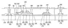
도 1은 본 발명의 실시예에 따른 박막 트랜지스터 어레이 기판의 구조를 개략적으로 도시한 배치도이다.1 is a layout view schematically illustrating a structure of a thin film transistor array substrate according to an exemplary embodiment of the present invention.
도 1에서 보는 바와 같이, 본 발명의 실시예에 따른 박막 트랜지스터 어레이 기판(100)에는 화상이 표시되는 다수의 화소가 매트릭스의 형태로 배열되어 있으며 주사 신호 또는 게이트 신호를 전달하는 게이트 배선(200)과 데이터 신호 또는 영상 신호를 전달하는 데이터 배선(700)과, 각각의 화소에 형성되어 있으며 투명한 도전 물질 또는 반사도를 가지는 도전 물질로 이루어진 화소 전극, 게이트 배선(200) 및 데이터 배선(700)과 전기적으로 연결되어 있으며 게이트 배선(200)의 주사 신호를 통하여 데이터 배선(700)을 경유하여 화소 전극에 전달되는 영상 신호를 제어하는 박막 트랜지스터 등이 배치되어 있는 화면 표시부(A)와 외부로부터의 주사 신호 또는 영상 신호를 게이트 배선(200) 또는 데이터 배선(700)으로 전달하는 게이트 패드 및 데이터 패드가 군집되어 형성되어 있는 게이트 및 데이터 패드 부(P)와 제조 공정 중에 발생하는 정전기를 방전시켜 화면 표시부에 형성되어 있는 박막 트랜지스터와 같은 소자가 파괴되는 것을 방지하기 위해 다수의 게이트 배선(200)과 데이터 배선(700)에 각각 연결되어 있는 저항 단차부(G)를 포함한다. 이때, 다수의 게이트 배선(200) 및 데이터 배선(700)은 게이트 및 데이터 패드부(P)와 저항 단차부(G)를 경유하여 게이트 단락선(128) 및 데이터 단락선(178)에 연결되어 있으며, 저항 단차부(G)와 게이트 단락선(128) 및 데이터 단락선(178)은 정전기 보호 소자에 속한다. 여기서, 저항 단차부(G)는 적어도 둘 이상이고 낮은 선 저항을 가지는 부분과 높은 선 저항을 가지는 부분을 포함하는 배선으로 이루어져 있으며, 제조 공정시에 정전기가 발생하는 경우 정전기는 게이트 및 데이터 단락선(128, 178)을 통하여 다수의 게이트 배선(200) 및 데이터 배선(700)으로 퍼지게 되는데, 게이트 배선(200) 및 데이터 배선(700)으로 흐르기 전에 저항 단차부(G)에서는 선 저항의 차이가 급격히 변화로 인하여 불꽃 방전(spark discharge)이 발생하며, 이러한 통하여 정전기는 방전된다.As shown in FIG. 1, in the thin film
다음은, 이러한 본 발명의 실시예에 따른 박막 트랜지스터 어레이 기판에서 화면 표시부, 저항 단차부 및 패드부에 대하여 도면을 참조하여 구체적으로 설명하기로 한다.Next, a screen display unit, a resistance step unit, and a pad unit in the thin film transistor array substrate according to the exemplary embodiment of the present invention will be described in detail with reference to the accompanying drawings.
먼저, 도 2 내지 도 4를 참고로 하여 본 발명의 제1 실시예에 따른 액정 표시 장치용 박막 트랜지스터 어레이 기판의 구조에 대하여 상세히 설명한다.First, the structure of the thin film transistor array substrate for a liquid crystal display according to the first embodiment of the present invention will be described in detail with reference to FIGS. 2 to 4.
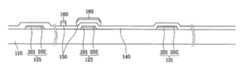
도 2는 본 발명의 제1 실시예에 따른 액정 표시 장치용 박막 트랜지스터 기판의 배치도이고, 도 3 및 도 4는 도 2에 도시한 박막 트랜지스터 어레이 기판을 III-III' 및 V-V' 선을 따라 잘라 도시한 각각의 단면도이다.2 is a layout view of a thin film transistor substrate for a liquid crystal display according to a first exemplary embodiment of the present invention, and FIGS. 3 and 4 are cut along the III-III 'and VV' lines of the thin film transistor array substrate shown in FIG. Each cross section is shown.
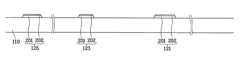
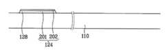
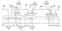
절연 기판(110) 위에는 높은 비저항을 가지는 몰리브덴 또는 몰리브덴 합금 또는 크롬 등으로 이루어진 하부막(201)과 하부막(201)보다 낮은 비저항을 가지는 은 또는 은 합금 또는 알루미늄 또는 알루미늄 합금 등으로 이루어진 상부막(202)을 포함하는 게이트 배선과 제1 정전기 보호용 배선이 테이퍼 구조로 형성되어 있다. 게이트 배선은 화면 표시부(A)에서 가로 방향으로 뻗어 있는 게이트선(121), 게이트선(121)의 끝에 연결되어 패드부(P)에 위치하며 외부로부터의 게이트 신호를 인가받아 게이트선(121)으로 전달하는 게이트 패드(125) 및 게이트선(121)에 연결되어 있으며 화면 표시부(A)에 위치하는 박막 트랜지스터의 게이트 전극(123)을 포함한다. 또한, 게이트 배선은 이후에 형성되는 화소 전극(190)과 연결되어 있는 유지 축전기용 도전체 패턴(177)과 중첩되어 화소의 전하 보존 능력을 향상시키는 유지 축전기를 이룬다. 제1 정전기 보호용 배선은 저항 단차부(G)에 형성되어 있으며 게이트선(121) 맞은편에서 게이트 패드(125)에 연결되어 있는 저항 단차용 연결선(124) 및 다수의 게이트선(121)을 저항 단차용 연결선(124)을 통하여 공통으로 연결하는 게이트 단락선(128)을 포함한다. 이때, 게이트 배선(121, 123, 125) 및 제1 정전기 보호용 배선(124, 128)은 30-70° 정도의 경사각을 가지는 테이퍼 구조로 형성되어 있다.On the insulating
기판(110) 위에는 질화 규소(SiNx) 따위로 이루어진 게이트 절연막(140)이 게이트 배선(121, 125, 123) 및 제1 정전기 보호용 배선(124, 128)을 덮고 있다.On the
게이트 전극(125)의 게이트 절연막(140) 상부에는 비정질 규소 등의 반도체로 이루어진 반도체층(150)이 형성되어 있으며, 반도체층(150)의 상부에는 실리사이드 또는 n형 불순물이 고농도로 도핑되어 있는 n+ 수소화 비정질 규소 따위의 물질로 만들어진 저항 접촉층(163, 165)이 각각 형성되어 있다.A
저항 접촉층(163, 165) 또는 게이트 절연막(140) 위에는 높은 비저항을 가지는 몰리브덴 또는 몰리브덴 합금 또는 크롬 등으로 이루어진 하부막(701)과 하부막(701)보다 낮은 비저항을 가지는 은 또는 은 합금 또는 알루미늄 또는 알루미늄 합금 등으로 이루어진 상부막(702)을 포함하는 데이터 배선과 제2 정전기 보호용 배선이 형성되어 있다. 데이터 배선은 화면 표시부(A)에서 세로 방향으로 뻗어 게이트선(121)과 교차하여 화소 영역을 정의하는 데이터선(171), 데이터선(171)에 연결되어 저항 접촉층(163)의 상부까지 연장되어 있는 소스 전극(173), 데이터선(171)의 한쪽 끝에 연결되어 패드부(P)에 있으며 외부로부터의 화상 신호를 인가받는 데이터 패드(179), 소스 전극(173)과 분리되어 있으며 게이트 전극(123)에 대하여 소스 전극(173)의 반대쪽 저항 접촉층(165) 상부에 형성되어 있는 드레인 전극(175)을 포함한다. 또한, 데이터 배선은 유지 용량을 향상시키기 위해 게이트선(121)과 중첩되어 있으며, 이후에 형성되는 화소 전극(190)과 전기적으로 연결되어 있는 유지 축전기용 도전체 패턴(177)을 포함할 수 있다. 제2 정전기 보호용 배선은 저항 단차부(G)에 형성되어 있으며 데이터선(111) 맞은편에서 데이터 패드(179)에 연결되어 있는 저항 단차용 연결선(174) 및 다수의 데이터선(171)을 저항 단차용 연결선(178)을 통하여 공통으로 연결하는 데이터 단락선(178)을 포함 한다.On the resistive contact layers 163 and 165 or the
데이터 배선(171, 173, 175, 177, 179), 제2 정전기 보호용 배선(174, 178) 및 이들이 가리지 않는 반도체층(150) 상부에는 평탄화 특성이 우수하며 감광성을 가지는 유기 물질 또는 a-Si:C:O:H 등을 포함하는 저유전율 절연 물질의 절연막을 포함하는 보호막(180)이 형성되어 있다. 여기서, 보호막(180)은 질화 규소로 이루어진 절연막을 더 포함할 수 있으며, 이러한 경우에 절연막은 유기 절연막의 하부에 위치하여 반도체층(150)을 직접 덮는 것이 바람직하다. 또한, 게이트 패드(125) 및 데이터 패드(179)가 위치하는 패드부(P)에서 유기 절연 물질은 완전히 제거하는 것이 바람직한데, 이러한 구조는 패드부에 게이트 패드(125) 및 데이터 패드(179)의 상부에 주사 신호 및 영상 신호를 각각 전달하기 위해 박막 트랜지스터 기판의 상부에 게이트 구동 집적 회로 및 데이터 구동 집적 회로를 직접 실장하는 COG(chip on glass) 방식의 액정 표시 장치에 적용할 때 특히 유리하다.On the
보호막(180)에는 드레인 전극(175), 유지 축전기용 도전체 패턴(177) 및 데이터 패드(179)를 각각 드러내는 접촉 구멍(185, 187, 189)이 형성되어 있으며, 게이트 절연막(140)과 함께 게이트 패드(125)를 드러내는 접촉 구멍(182)이 형성되어 있다. 또한, 보호막(180)에는 저항 단차용 연결선(124, 174)을 드러내는 접촉 구멍(184, 186)이 적어도 둘 이상 형성되어 있다. 이때, 접촉 구멍(184, 186)은 저항 단차용 연결선(124, 174)의 경계선이 드러내는 것이 바람직하며, 그렇지 않을 수도 있다. 여기서, 접촉 구멍(124, 174)을 통하여 통하여 드러난 저항 단차용 연결선(124, 174)에서는 낮은 비저항을 가지는 상부막(202, 702)이 제거되어 저항 단 차용 연결선(124, 174)의 다른 부분보다 접촉 구멍(184, 186)을 통하여 드러난 부분은 높은 선 저항을 가지게 된다. 따라서, 제조 공정시에 정전기가 발생하는 경우 정전기는 게이트 및 데이터 단락선(128, 178)을 통하여 다수의 게이트 배선(200) 및 데이터 배선(700)으로 퍼지게 되는데, 게이트 배선(200) 및 데이터 배선(700)으로 흐르기 전에 접촉 구멍(184, 186)에서 제거된 상부막(202, 702) 경계에서는 선 저항의 급격한 변화로 인하여 불꽃 방전(spark discharge)이 발생하며, 이러한 통하여 정전기는 방전된다. 여기서, 제조 공정시 불꽃 방전을 통하여 하부막(201, 701)은 단선될 수도 있다.In the
보호막(180) 상부에는 접촉 구멍(185)을 통하여 드레인 전극(175)과 전기적으로 연결되어 있고 화면 표시부(A)의 화소 영역에 위치하며, 투명한 도전 물질인 IZO(indium zinc oxide) 또는 ITO(indium tin oxide) 등으로 이루어진 화소 전극(190)이 형성되어 있다. 또한, 보호막(180) 위에는 접촉 구멍(182, 189)을 통하여 각각 게이트 패드(125) 및 데이터 패드(179)와 연결되어 있는 보조 게이트 패드(92) 및 보조 데이터 패드(97)가 패드부(P)에 형성되어 있다. 여기서, 보조 게이트 및 데이터 패드(92, 97)는 게이트 및 데이터 패드(125, 179)를 보호하기 위한 것이며, 필수적인 것은 아니다. 또한 보호막(180) 위에는 접촉 구멍(184, 186)을 통하여 저항 단차용 연결선(124, 174)에 접촉하는 저항 단차용 도전막(94, 96)이 형성되어 있다.An upper portion of the
이러한 본 발명의 제1 실시예에 따른 박막 트랜지스터 기판은 낮은 비저항을 가지는 배선을 포함하고 있어 대화면의 액정 표시 장치의 동작 특성을 향상시킬 수 있으며, 제1 및 제2 정전기 보호용 배선을 통하여 제조 공정시 발생하는 정전기를 용이하게 방전시킬 수 있는 효과가 있다.The thin film transistor substrate according to the first exemplary embodiment of the present invention includes a wiring having a low specific resistance, thereby improving operating characteristics of the liquid crystal display of the large screen, and during the manufacturing process through the first and second electrostatic protection wirings. There is an effect that can easily discharge the static electricity generated.
그러면, 도 5a 내지 도 8c 및 도 2 내지 도 4를 참조하여 본 발명의 실시예에 따른 박막 트랜지스터 어레이 기판의 제조 방법에 대하여 구체적으로 설명하기로 한다.Next, a method of manufacturing a thin film transistor array substrate according to an exemplary embodiment of the present invention will be described in detail with reference to FIGS. 5A to 8C and FIGS. 2 to 4.
먼저, 도 5a 내지 도 5c에 도시한 바와 같이, 유리 기판(110) 상부에 몰리브덴 또는 몰리브덴 합금 또는 크롬 등의 하부막(201)과 하부막(201)보다 낮은 비저항을 가지는 알루미늄 또는 알루미늄 합금 등의 상부막(202)을 차례로 적층하고, 마스크를 이용한 사진 식각 공정으로 상부막(202)과 하부막(201)을 함께 패터닝하여 게이트선(121), 게이트 전극(123) 및 게이트 패드(125)를 포함하는 게이트 배선과 게이트 단락선(128) 및 저항 단차용 연결선(14)을 포함하는 제1 정전기 보호용 배선을 테이퍼 구조로 형성한다.First, as shown in FIGS. 5A to 5C, the
다음, 도 6a 내지 도 6c에 도시한 바와 같이, 질화 규소로 이루어진 게이트 절연막(140), 비정질 규소로 이루어진 반도체층(150), 도핑된 비정질 규소층(160)의 삼층막을 연속하여 적층하고 마스크를 이용한 패터닝 공정으로 반도체층(150)과 도핑된 비정질 규소층(160)을 패터닝하여 게이트 전극(125)과 마주하는 게이트 절연막(140) 상부에 반도체층(150)과 저항 접촉층(160)을 형성한다.Next, as shown in FIGS. 6A to 6C, three layers of the
다음, 도 7a 내지 도 7b에 도시한 바와 같이, 몰리브덴 또는 몰리브덴 합금 또는 크롬 등의 하부막(701)과 하부막(701)보다 낮은 비저항을 가지는 알루미늄 또는 알루미늄 합금 등의 상부막(702)을 차례로 적층하고, 마스크를 이용한 사진 식 각 공정으로 상부막(702)과 하부막(701)을 함께 패터닝하여 게이트선(121)과 교차하는 데이터선(171), 데이터선(171)과 연결되어 게이트 전극(123) 상부까지 연장되어 있는 소스 전극(173), 데이터선(171)은 한쪽 끝에 연결되어 있는 데이터 패드(179), 소스 전극(173)과 분리되어 있으며 게이트 전극(123)을 중심으로 소스 전극(173)과 마주하는 드레인 전극(175) 및 유지 축전기용 도전체 패턴(177)을 포함하는 데이터 배선과 데이터 단락선(178) 및 저항 단차용 연결선(174)을 포함하는 제2 정전기 보호용 배선을 테이퍼 구조로 형성한다.Next, as shown in FIGS. 7A to 7B, the
이어, 데이터 배선(171, 173, 175, 177, 179)으로 가리지 않는 도핑된 비정질 규소층 패턴(160)을 식각하여 게이트 전극(123)을 중심으로 양쪽으로 분리시키는 한편, 양쪽의 도핑된 비정질 규소층(163, 165) 사이의 반도체층 패턴(150)을 노출시킨다. 이어, 노출된 반도체층(150)의 표면을 안정화시키기 위하여 산소 플라스마를 실시하는 것이 바람직하다.Next, the doped amorphous
다음으로, 도 9a 및 9b에서 보는 바와 같이, 질화 규소를 적층하거나 또는 평탄화 특성이 우수하며 감광성을 가지는 유기 물질을 기판(110)의 상부에 코팅(coating)하거나 PECVD(plasma enhanced chemical vapor deposition) 방법으로 a-Si:C:O 막 또는 a-Si:O:F 막 등의 저유전율 CVD막을 증착하여 보호막(180)을 형성한다. 이어, 마스크를 이용한 사진 식각 공정으로 게이트 절연막(140)과 함께 패터닝하여, 게이트 패드(125), 드레인 전극(175), 데이터 패드(179) 및 유지 축전기용 도전체 패턴(177)을 드러내는 접촉 구멍(182, 185, 189, 187)과 제1 및 제2 정전기 보호용 배선의 저항 단차용 연결선(174, 124)을 드러내는 접촉 구멍(184, 186)을 하나 이상 형성한다. 이어, 알루미늄 식각액을 이용한 알루미늄 전면 식각 공정을 통하여 접촉 구멍(182, 185, 189, 187, 174, 124)을 통하여 드러난 상부막(202, 702)을 제거한다. 이렇게, 접촉부에서 접촉 구멍(182, 185, 189, 187)을 통하여 드러난 게이트 패드(125), 드레인 전극(175), 데이터 패드(179) 및 유지 축전기용 도전체 패턴(177)의 상부막(202, 702)을 제거할 때, 저항 단차용 연결선(174, 124)을 드러내는 접촉 구멍(184, 186)을 통하여 드러난 상부막(202, 702)을 제거함으로써 추가되는 공정 없이 저항 단차용 연결선(174, 124)에 선 저항이 다른 두 부분을 형성할 수 있다.Next, as shown in FIGS. 9A and 9B, silicon nitride is deposited or an organic material having excellent planarization characteristics and a photosensitive property is coated on the
다음, 도 2 내지 도 4에서 보는 바와 같이, 투명 도전 물질을 증착하고 마스크를 이용한 사진 식각 공정으로 패터닝하여 접촉 구멍(187, 185)을 통하여 드레인 전극(175) 및 유지 축전기용 도전체 패턴(177)의 하부막(701)과 연결되는 화소 전극(190)과 접촉 구멍(182, 189)을 통하여 게이트 패드(125) 및 데이터 패드(179)의 하부막(201, 701)과 각각 연결되는 보조 게이트 패드(92) 및 보조 데이터 패드(97)를 각각 형성한다. 또한, 접촉 구멍(184, 186)을 통하여 드러난 저항 단차용 연결선(174, 124)의 하부막(201, 701)과 연결되는 저항 단차용 도전막(94, 96)을 형성한다.Next, as shown in FIGS. 2 to 4, a transparent conductive material is deposited and patterned by a photolithography process using a mask to form the
이후의 제조 공정에서 제1 및 제2 정전기 보호용 배선(124, 128, 174, 178)은 게이트 배선 및 데이터 배선의 단선 및 단락 또는 화소의 결합을 검사할 때 전기적인 신호를 인가하기 위한 배선으로 사용된다. 또한, 이후의 제조 공정시에 발생하는 정전기로부터 화면 표시부의 박막 트랜지스터가 손상되는 것을 방지하기 위 한 정전기 보호 소자로 사용되며, 방전시 제1 및 제2 정전기 보호용 배선(124, 128, 174, 178) 중 상부막(202, 702)이 제거된 부분에서 단선이 발생할 수 있다. 여기서, 박막 트랜지스터 어레이 기판과 이와 마주하는 대향 기판을 결합하여 액정 표시 장치를 완성한 다음에는 게이트 배선 및 데이터 배선으로부터 제1 및 제2 정전기 보호용 배선(124, 128, 174, 178)을 전기적으로 분리한다.In the subsequent manufacturing process, the first and second static
앞에서는 반도체층과 데이터 배선을 서로 다른 마스크를 이용한 사진 식각 공정으로 형성하는 제조 방법에 본 발명의 실시예를 적용하여 설명하였지만, 본 발명의 실시예는 제조 비용을 최소화하기 위하여 반도체층과 데이터 배선을 하나의 감광막 패턴을 이용한 사진 식각 공정으로 형성하는 액정 표시 장치용 박막 트랜지스터 어레이 기판의 제조 방법에서도 동일하게 적용할 수 있다. 이에 대하여 도면을 참조하여 상세하게 설명하기로 한다.In the above, the embodiment of the present invention has been described in the manufacturing method of forming the semiconductor layer and the data wiring by a photolithography process using different masks. However, the embodiment of the present invention provides the semiconductor layer and the data wiring in order to minimize manufacturing costs. The same applies to the method of manufacturing a thin film transistor array substrate for a liquid crystal display device, which is formed by a photolithography process using one photosensitive film pattern. This will be described in detail with reference to the drawings.
먼저, 도 9 내지 도 12를 참고로 하여 본 발명의 제2 실시예에 따른 액정 표시 장치용 박막 트랜지스터 기판의 단위 화소 구조에 대하여 상세히 설명한다.First, the unit pixel structure of the thin film transistor substrate for a liquid crystal display according to the second exemplary embodiment of the present invention will be described in detail with reference to FIGS. 9 to 12.
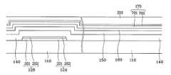
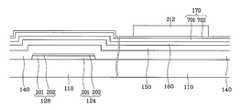
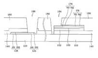
도 9는 본 발명의 제2 실시예에 따른 액정 표시 장치용 박막 트랜지스터 기판의 배치도이고, 도 10 내지 도 12는 각각 도 9에 도시한 박막 트랜지스터 기판을 X-X' 선, XI-XI' 선 및 XII-XII' 선을 따라 잘라 도시한 단면도이다.9 is a layout view of a thin film transistor substrate for a liquid crystal display according to a second exemplary embodiment of the present invention, and FIGS. 10 to 12 are lines XX ′, XI-XI ′, and XII of the thin film transistor substrate illustrated in FIG. 9, respectively. A cross-sectional view taken along the line -XII '.
먼저, 절연 기판(110) 위에 제1 실시예와 동일하게 하부막(201) 및 하부막 보다 낮은 비저항을 가지는 상부막(202)을 포함하며, 게이트선(121), 게이트 패드(125) 및 게이트 전극(123)을 포함하는 게이트 배선 및 게이트 단락선(128) 및 저항 단차용 연결선(124)을 포함하는 제1 정전기 보호용 배선이 테이퍼 구조로 형 성되어 있다. 그리고, 기판(110) 상부에는 게이트선(121)과 평행하며 상판의 공통 전극에 입력되는 공통 전극 전압 따위의 전압을 외부로부터 인가받는 유지 전극선(131) 및 유지 전극선(131)에 연결되어 있는 유지 전극(133)을 포함하는 유지 배선이 형성되어 있다. 유지 전극(133)은 후술할 화소 전극(190)과 연결된 유지 축전기용 도전체 패턴(177)과 중첩되어 화소의 전하 보존 능력을 향상시키는 유지 축전기를 이루며, 후술할 화소 전극(190)과 게이트선(121)의 중첩으로 발생하는 유지 용량이 충분할 경우 형성하지 않을 수도 있다. 이때, 게이트 배선(121, 123, 125), 유지 배선(131, 133) 및 제1 정전기 보호용 배선(124, 128)은 30-70° 정도의 경사각을 가지는 테이퍼 구조를 가진다.First, the
게이트 배선(121, 125, 123), 제1 정전기 보호용 배선(124, 128) 및 유지 배선(131, 133) 위에는 질화 규소(SiNx) 따위로 이루어진 게이트 절연막(140)이 형성되어 게이트 배선(121, 125, 123)과 제1 정전기 보호용 배선(124, 128)과 유지 배선(131, 133)을 덮고 있다.A
게이트 절연막(140) 위에는 다결정 규소 또는 비정질 규소 등으로 이루어진 반도체 패턴(152, 157)이 형성되어 있으며, 반도체 패턴(152, 157) 위에는 인(P) 따위의 n형 또는 p형 불순물로 고농도로 도핑되어 있는 비정질 규소 따위로 이루어진 저항성 접촉층(ohmic contact layer) 패턴 또는 중간층 패턴(163, 165, 167)이 형성되어 있다.The
저항성 접촉층 패턴(163, 165, 167) 위에는 제1 실시예와 동일하게 하부막(701)과 하부막(701)보다 낮은 비저항을 가지는 상부막(702)을 포함하는 데이터 배선과 제2 정전기 보호용 배선이 테이퍼 구조로 형성되어 있다. 데이터 배선은 세로 방향으로 형성되어 있는 데이터선(171), 데이터선(171)의 한쪽 끝에 연결되어 외부로부터의 화상 신호를 인가받는 데이터 패드(179), 그리고 데이터선(171)의 분지인 박막 트랜지스터의 소스 전극(173)으로 이루어진 데이터선부를 포함하며, 또한 데이터선부(171, 179, 173)와 분리되어 있으며 게이트 전극(123) 또는 박막 트랜지스터의 채널부(C)에 대하여 소스 전극(173)의 반대쪽에 위치하는 박막 트랜지스터의 드레인 전극(175)과 유지 전극(133) 위에 위치하고 있는 유지 축전기용 도전체 패턴(177)도 포함한다. 유지 배선(131, 133)을 형성하지 않을 경우 유지 축전기용 도전체 패턴(177) 또한 형성하지 않는다. 여기서, 유지 축전기용 도전체 패턴(177)이 드레인 전극(175)에 연결되어 있지만, 그렇지 않을 수도 있다. 제2 정전기 보호용 배선은 저항 단차부(G)에 형성되어 있으며 데이터선(111) 맞은편에서 데이터 패드(179)에 연결되어 있는 저항 단차용 연결선(174) 및 다수의 데이터선(171)을 저항 단차용 연결선(178)을 통하여 공통으로 연결하는 데이터 단락선(178)을 포함한다. 이때, 데이터 배선(171, 173, 175, 177, 179) 및 제2 정전기 보호용 배선(174, 178)은 30-80° 정도의 경사각을 가지는 테이퍼 구조를 가질 수 있으며, 접촉층 패턴(163, 165, 167)은 그 하부의 반도체 패턴(152, 157) 또한 그러하다.On the ohmic
접촉층 패턴(163, 165, 167)은 그 하부의 반도체 패턴(152, 157)과 그 상부의 데이터 배선(171, 173, 175, 177, 179)의 접촉 저항을 낮추어 주는 역할을 하 며, 데이터 배선(171, 173, 175, 177, 179) 및 제2 정전기 보호용 배선(174, 178)과 완전히 동일한 형태를 가진다. 즉, 데이터선부 중간층 패턴(163)은 데이터선부(171, 179, 173)와 동일하고, 드레인 전극용 중간층 패턴(163)은 드레인 전극(173)과 동일하며, 유지 축전기용 중간층 패턴(167)은 유지 축전기용 도전체 패턴(177)과 동일하다.The
한편, 반도체 패턴(152, 157)은 박막 트랜지스터의 채널부(C)를 제외하면 데이터 배선(171, 173, 175, 177, 179), 제2 정전기 보호용 배선(174, 178) 및 저항성 접촉층 패턴(163, 165, 167)과 동일한 모양을 하고 있다. 구체적으로는, 유지 축전기용 반도체 패턴(157)과 유지 축전기용 도전체 패턴(177) 및 유지 축전기용 접촉층 패턴(167)은 동일한 모양이지만, 박막 트랜지스터용 반도체 패턴(152)은 데이터 배선 및 접촉층 패턴의 나머지 부분과 약간 다르다. 즉, 박막 트랜지스터의 채널부(C)에서 데이터선부(171, 179, 173), 특히 소스 전극(173)과 드레인 전극(175)이 분리되어 있고 데이터선부 중간층(163)과 드레인 전극용 접촉층 패턴(165)도 분리되어 있으나, 박막 트랜지스터용 반도체 패턴(152)은 이곳에서 끊어지지 않고 연결되어 박막 트랜지스터의 채널을 생성한다.The
데이터 배선(171, 173, 175, 177, 179) 및 데이터 배선으로 가리지 않는 반도체층(152) 상부에는 질화 규소 또는 산화 규소로 이루어진 절연막 또는 낮은 유전율을 가지는 유기 물질로 이루어진 유기 절연막 또는 저유전율 CVD막을 포함하는 보호막(180)이 형성되어 있다.An insulating film made of silicon nitride or silicon oxide or an organic insulating film made of an organic material having a low dielectric constant or a low dielectric constant CVD film is disposed on the data wirings 171, 173, 175, 177, and 179 and the
보호막(180)은 데이터 패드(179) 및 유지 축전기용 도전체 패턴(177)을 드러 내는 접촉 구멍(189, 187)을 가지고 있으며, 또한 게이트 절연막(140)과 함께 게이트 패드(125)를 드러내는 접촉 구멍(182)을 가지고 있다. 또한, 제1 및 제2 정전기 보호용 배선(124, 128, 174, 178)의 저항 단타용 연결선(124, 174)을 드러내는 접촉 구멍(184, 186)을 가지고 있다. 제1 실시예와 동일하게 접촉 구멍(184, 186, 187, 189)에서는 상부막(202, 702)이 제거되어 하부막(201, 701)이 드러나 있다.The
보호막(180) 위에는 박막 트랜지스터로부터 화상 신호를 받아 상판의 전극과 함께 전기장을 생성하는 화소 전극(190)이 형성되어 있다. 화소 전극(190)은 IZO 또는 ITO 따위의 투명한 도전 물질로 이루어져 있으며 접촉 구멍(187)을 통하여 드레인 전극(175)과 연결되어 있는 유지 축전기용 도전체 패턴(177)과 물리적·전기적으로 연결되어 화상 신호를 전달받는다. 화소 전극(190)은 또한 이웃하는 게이트선(121) 및 데이터선(171)과 중첩되어 개구율을 높이고 있으나, 중첩되지 않을 수도 있다. 화소 전극(190)은 접촉 구멍(187)을 통하여 유지 축전기용 도전체 패턴(177)과도 연결되어 도전체 패턴(177)으로 화상 신호를 전달한다. 한편, 게이트 패드(125) 및 데이터 패드(179) 위에는 접촉 구멍(182, 189)을 통하여 각각 이들과 연결되는 보조 게이트 패드(92) 및 보조 데이터 패드(97)가 형성되어 있으며, 이들은 패드(125, 179)와 외부 회로 장치와의 접착성을 보완하고 패드를 보호하는 역할을 하는 것으로 필수적인 것은 아니며, 이들의 적용 여부는 선택적이다. 또한 보호막(180) 위에는 접촉 구멍(184, 186)을 통하여 저항 단차용 연결선(124, 174)에 접촉하는 저항 단차용 도전막(94, 96)이 형성되어 있다.A
그러면, 도 9 내지 도 12의 구조를 가지는 액정 표시 장치용 박막 트랜지스 터 어레이 기판을 제조하는 방법에 대하여 상세하게 도 9 내지 도 12와 도 13a 내지 도 19d를 참조하여 설명하기로 한다.Next, a method of manufacturing a thin film transistor array substrate for a liquid crystal display device having the structure of FIGS. 9 to 12 will be described with reference to FIGS. 9 to 12 and 13A to 19D.
먼저, 도 13a 내지 13d에 도시한 바와 같이, 제1 실시예와 동일하게 하부막(701)과 하부막(701)보다 낮은 비저항을 가지는 상부막(702)을 차례로 적층하고 마스크를 이용한 사진 식각 공정으로 패터닝하여 게이트선(121), 게이트 패드(125) 및 게이트 전극(123)을 포함하는 게이트 배선과 유지 전극선(131) 및 유지 전극(133)을 포함하는 유지 배선과 게이트 단락선(128) 및 저항 단차용 연결선(124)을 포함하는 제1 정전기 보호용 배선을 테이퍼 구조로 형성한다.First, as shown in FIGS. 13A to 13D, similarly to the first embodiment, the
다음, 도 14a 내지 14c에 도시한 바와 같이, 질화 규소로 이루어진 게이트 절연막(140), 도핑되지 않은 비정질 규소의 반도체층(150), 도핑된 비정질 규소의 중간층(160)을 화학 기상 증착법을 이용하여 각각 1,500 Å 내지 5,000 Å, 500 Å 내지 2,000 Å, 1400 Å 내지 600 Å의 두께로 연속 증착한다. 이어, 제1 실시예와 동일하게 하부막(701)과 하부막(701)보다 낮은 비저항을 가지는 상부막(702)을 포함하는 도전체층(170)을 스퍼터링 등의 방법으로 1,500 Å 내지 3,000 Å의 두께로 증착한 다음 그 위에 감광막(210)을 1 μm 내지 2 μm의 두께로 도포한다.Next, as shown in FIGS. 14A to 14C, the
그 후, 마스크를 통하여 감광막(210)에 빛을 조사한 후 현상하여 도 15b 내지 15d에 도시한 바와 같이, 감광막 패턴(212, 214)을 형성한다. 이때, 감광막 패턴(212, 214) 중에서 박막 트랜지스터의 채널부(C), 즉 소스 전극(173)과 드레인 전극(175) 사이에 위치한 제1 부분(214)은 배선부(A), 즉 데이터 배선(171, 173, 175, 177, 179) 및 제2 정전기 보호용 배선(174, 178)이 형성될 부분에 위치한 제2 부분(212)보다 두께가 작게 되도록 하며, 기타 부분(B)의 감광막은 모두 제거한다. 이 때, 채널부(C)에 남아 있는 감광막(214)의 두께와 데이터 배선부(A)에 남아 있는 감광막(212)의 두께의 비는 후에 후술할 식각 공정에서의 공정 조건에 따라 다르게 하여야 하되, 제1 부분(214)의 두께를 제2 부분(212)의 두께의 1/2 이하로 하는 것이 바람직하며, 예를 들면, 4,000 Å 이하인 것이 좋다.Thereafter, the
이와 같이, 위치에 따라 감광막의 두께를 달리하는 방법으로 여러 가지가 있을 수 있으며, A 영역의 빛 투과량을 조절하기 위하여 주로 슬릿(slit)이나 격자 형태의 패턴을 형성하거나 반투명막을 사용한다.As such, there may be various methods of varying the thickness of the photoresist layer according to the position. In order to control the light transmittance in the A region, a slit or lattice-shaped pattern is mainly formed or a translucent film is used.
이때, 슬릿 사이에 위치한 패턴의 선 폭이나 패턴 사이의 간격, 즉 슬릿의 폭은 노광시 사용하는 노광기의 분해능보다 작은 것이 바람직하며, 반투명막을 이용하는 경우에는 마스크를 제작할 때 투과율을 조절하기 위하여 다른 투과율을 가지는 박막을 이용하거나 두께가 다른 박막을 이용할 수 있다.In this case, the line width of the pattern located between the slits or the interval between the patterns, that is, the width of the slits, is preferably smaller than the resolution of the exposure machine used for exposure, and in the case of using a translucent film, the transmittance is different in order to control the transmittance when fabricating a mask. A thin film having a thickness or a thin film may be used.
이와 같은 마스크를 통하여 감광막에 빛을 조사하면 빛에 직접 노출되는 부분에서는 고분자들이 완전히 분해되며, 슬릿 패턴이나 반투명막이 형성되어 있는 부분에서는 빛의 조사량이 적으므로 고분자들은 완전 분해되지 않은 상태이며, 차광막으로 가려진 부분에서는 고분자가 거의 분해되지 않는다. 이어 감광막을 현상하면, 고분자 분자들이 분해되지 않은 부분만이 남고, 빛이 적게 조사된 중앙 부분에는 빛에 전혀 조사되지 않은 부분보다 얇은 두께의 감광막이 남길 수 있다. 이때, 노광 시간을 길게 하면 모든 분자들이 분해되므로 그렇게 되지 않도록 해야 한다.When the light is irradiated to the photosensitive film through such a mask, the polymers are completely decomposed at the part directly exposed to the light, and the polymers are not completely decomposed because the amount of light is small at the part where the slit pattern or the translucent film is formed. In the area covered by, the polymer is hardly decomposed. Subsequently, when the photoresist film is developed, only a portion where the polymer molecules are not decomposed is left, and a thin photoresist film may be left at a portion where the light is not irradiated at a portion less irradiated with light. In this case, if the exposure time is extended, all molecules are decomposed, so it should not be so.
이러한 얇은 두께의 감광막(214)은 리플로우가 가능한 물질로 이루어진 감광막을 이용하고 빛이 완전히 투과할 수 있는 부분과 빛이 완전히 투과할 수 없는 부분으로 나뉘어진 통상적인 마스크로 노광한 다음 현상하고 리플로우시켜 감광막이 잔류하지 않는 부분으로 감광막의 일부를 흘러내리도록 함으로써 형성할 수도 있다.The
이어, 감광막 패턴(214) 및 그 하부의 막들, 즉 도전체층(170), 중간층(160) 및 반도체층(150)에 대한 식각을 진행한다. 이때, 배선부(A)에는 데이터 배선과 제2 정전기 보호용 배선 및 그 하부의 막들이 그대로 남아 있고, 채널부(C)에는 반도체층만 남아 있어야 하며, 나머지 부분(B)에는 위의 3개 층(170, 160, 150)이 모두 제거되어 게이트 절연막(140)이 드러나야 한다.Subsequently, etching is performed on the
먼저, 도 16a 내지 16c에 도시한 것처럼, 기타 부분(B)의 노출되어 있는 도전체층(170)을 제거하여 그 하부의 중간층(160)을 노출시킨다. 이 과정에서는 건식 식각 또는 습식 식각 방법을 모두 사용할 수 있으며, 이때 도전체층(170)은 식각되고 감광막 패턴(212, 214)은 거의 식각되지 않는 조건하에서 행하는 것이 좋다. 그러나, 건식 식각의 경우 도전체층(170)만을 식각하고 감광막 패턴(212, 214)은 식각되지 않는 조건을 찾기가 어려우므로 감광막 패턴(212, 214)도 함께 식각되는 조건하에서 행할 수 있다. 이 경우에는 습식 식각의 경우보다 제1 부분(214)의 두께를 두껍게 하여 이 과정에서 제1 부분(214)이 제거되어 하부의 도전체층(170)이 드러나는 일이 생기지 않도록 한다.First, as shown in FIGS. 16A to 16C, the exposed
이렇게 하면, 도 16a 내지 도 16c에 나타낸 것처럼, 채널부(C) 및 데이터 배 선부(A)의 도전체층(176)과 유지 축전기용 도전체 패턴(177)만이 남고 기타 부분(B)의 도전체층(170)은 모두 제거되어 그 하부의 중간층(160)이 드러난다. 이때 남은 도전체 패턴(176, 177)은 소스 및 드레인 전극(173, 175)이 분리되지 않고 연결되어 있는 점을 제외하면 데이터 배선(171, 177, 173, 175, 179) 및 제2 정전기 보호용 배선(174, 178)의 형태와 동일하다. 또한 건식 식각을 사용한 경우 감광막 패턴(212, 214)도 어느 정도의 두께로 식각된다.In this way, as shown in FIGS. 16A to 16C, only the
이어, 도 17a 내지 17c에 도시한 바와 같이, 기타 부분(B)의 노출된 중간층(160) 및 그 하부의 반도체층(150)을 감광막의 제1 부분(214)과 함께 건식 식각 방법으로 동시에 제거한다. 이 때의 식각은 감광막 패턴(212, 214)과 중간층(160) 및 반도체층(150)(반도체층과 중간층은 식각 선택성이 거의 없음)이 동시에 식각되며 게이트 절연막(140)은 식각되지 않는 조건하에서 행하여야 하며, 특히 감광막 패턴(212, 214)과 반도체층(150)에 대한 식각비가 거의 동일한 조건으로 식각하는 것이 바람직하다. 예를 들어, SF6과 HCl의 혼합 기체나, SF6과 O2의 혼합 기체를 사용하면 거의 동일한 두께로 두 막을 식각할 수 있다. 감광막 패턴(212, 214)과 반도체층(150)에 대한 식각비가 동일한 경우 제1 부분(214)의 두께는 반도체층(150)과 중간층(160)의 두께를 합한 것과 같거나 그보다 작아야 한다.Then, as shown in FIGS. 17A to 17C, the exposed
이렇게 하면, 도 17a 내지 17c에 나타낸 바와 같이, 채널부(C)의 제1 부분(214)이 제거되어 소스/드레인용 도전체 패턴(176)이 드러나고, 기타 부분(B) 의 중간층(160) 및 반도체층(150)이 제거되어 그 하부의 게이트 절연막(140)이 드러난다. 한편, 데이터 배선부(A)의 제2 부분(212) 역시 식각되므로 두께가 얇아진다. 또한, 이 단계에서 반도체 패턴(152, 157)이 완성된다. 도면 부호 168과 167은 각각 소스/드레인용 도전체 패턴(176) 하부의 중간층 패턴과 유지 축전기용 도전체 패턴(177) 하부의 중간층 패턴을 가리킨다.This removes the
이어 애싱(ashing)을 통하여 채널부(C)의 소스/드레인용 도전체 패턴(178) 표면에 남아 있는 감광막 찌꺼기를 제거한다.Subsequently, ashing of the photoresist film remaining on the surface of the source /
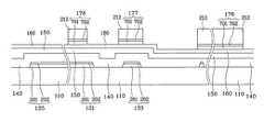
다음, 도 18a 내지 18b에 도시한 바와 같이 채널부(C)의 소스/드레인용 도전체 패턴(176) 및 그 하부의 소스/드레인용 중간층 패턴(168)을 식각하여 제거한다. 이 때, 식각은 소스/드레인용 도전체 패턴(176)과 중간층 패턴(168) 모두에 대하여 건식 식각만으로 진행할 수도 있으며, 소스/드레인용 도전체 패턴(176)에 대해서는 습식 식각으로, 중간층 패턴(168)에 대해서는 건식 식각으로 행할 수도 있다. 전자의 경우 소스/드레인용 도전체 패턴(176)과 중간층 패턴(168)의 식각 선택비가 큰 조건하에서 식각을 행하는 것이 바람직하며, 이는 식각 선택비가 크지 않을 경우 식각 종점을 찾기가 어려워 채널부(C)에 남는 반도체 패턴(152)의 두께를 조절하기가 쉽지 않기 때문이다. 중간층 패턴(168) 및 반도체 패턴(152)을 식각할 때 사용하는 식각 기체의 예로는 앞에서 언급한 CF4와 HCl의 혼합 기체나 CF4와 O2의 혼합 기체를 들 수 있으며, CF4와 O2를 사용하면 균일한 두께로 반도체 패턴(152)을 남길 수 있다. 이때, 도 18b에 도시한 것처럼 반도체 패턴(152)의 일부가 제거되 어 두께가 작아질 수도 있으며 감광막 패턴의 제2 부분(212)도 이때 어느 정도의 두께로 식각된다. 이때의 식각은 게이트 절연막(140)이 식각되지 않는 조건으로 행하여야 하며, 제2 부분(212)이 식각되어 그 하부의 데이터 배선(171, 173, 175, 177, 179) 및 제2 정전기 보호용 배선(174, 178)이 드러나는 일이 없도록 감광막 패턴이 두꺼운 것이 바람직함은 물론이다.Next, as illustrated in FIGS. 18A to 18B, the source /
이렇게 하면, 소스 전극(173)과 드레인 전극(175)이 분리되면서 데이터 배선(171, 173, 175, 177, 179) 및 제2 정전기 보호용 배선(174, 178)과 그 하부의 접촉층 패턴(163, 165, 167)이 완성된다.In this case, the
마지막으로 배선부(A)에 남아 있는 감광막 제2 부분(212)을 제거한다. 그러나, 제2 부분(212)의 제거는 채널부(C) 소스/드레인용 도전체 패턴(176)을 제거한 후 그 밑의 중간층 패턴(168)을 제거하기 전에 이루어질 수도 있다.Finally, the photosensitive film
앞에서 설명한 것처럼, 습식 식각과 건식 식각을 교대로 하거나 건식 식각만을 사용할 수 있다. 후자의 경우에는 한 종류의 식각만을 사용하므로 공정이 비교적 간편하지만, 알맞은 식각 조건을 찾기가 어렵다. 반면, 전자의 경우에는 식각 조건을 찾기가 비교적 쉬우나 공정이 후자에 비하여 번거로운 점이 있다.As mentioned earlier, wet and dry etching can be alternately used or only dry etching can be used. In the latter case, since only one type of etching is used, the process is relatively easy, but it is difficult to find a suitable etching condition. On the other hand, in the former case, the etching conditions are relatively easy to find, but the process is more cumbersome than the latter.
이와 같이 하여 데이터 배선(171, 173, 175, 177, 179) 및 제2 정전기 보호용 배선(174, 178)을 형성한 후, 도 19a 내지 19d에 도시한 바와 같이 제1 실시예와 같은 절연 물질을 적층하여 보호막(180)을 형성하고, 마스크를 이용하여 보호막(180)을 게이트 절연막(140)과 함께 식각하여 게이트 패드(125), 데이터 패드(179) 및 유지 축전기용 도전체 패턴(177)을 각각 드러내는 접촉 구멍(182, 189, 187) 및 적어도 하나 이상의 저항 단차용 연결선(124, 174)을 드러내는 접촉 구멍(184, 186)을 형성한다. 이어, 알루미늄 식각액을 이용한 알루미늄 전면 식각 공정을 통하여 접촉 구멍(184, 186, 187, 189)을 통하여 드러난 알루미늄 또는 알루미늄 합금의 상부막(202, 702)을 제거한다.After the data wirings 171, 173, 175, 177, and 179 and the second
이어, 도 9 내지 도 12에 도시한 바와 같이, 500 Å 내지 1,000 Å 두께의 IZO 또는 ITO를 증착하고 마스크를 사용하여 식각하여 드레인 전극(175) 및 유지 축전기용 도전체 패턴(177)과 연결된 화소 전극(190), 게이트 패드(125)와 연결된 보조 게이트 패드(92) 및 데이터 패드(179)와 연결된 보조 데이터 패드(97)를 형성하고, 접촉 구멍(184, 186)을 통하여 저항 단차용 연결선(124, 174)의 하부막(201, 701)과 접촉하는 저항 단차용 도전막(94, 96)을 형성한다.9 to 12, a pixel connected to the
이러한 본 발명의 제2 실시예에서는 제1 실시예에 따른 효과뿐만 아니라 데이터 배선(171, 173, 175, 177, 179)과 그 하부의 접촉층 패턴(163, 165, 167) 및 반도체 패턴(152, 157)을 하나의 마스크를 이용하여 형성하고 이 과정에서 소스 전극(173)과 드레인 전극(175)이 분리하여 제조 공정을 단순화할 수 있다.In the second embodiment of the present invention, the data wirings 171, 173, 175, 177, and 179, the
이상에서 본 발명의 바람직한 실시예에 대하여 상세하게 설명하였지만 본 발명의 권리범위는 이에 한정되는 것은 아니고 다음의 청구범위에서 정의하고 있는 본 발명의 기본 개념을 이용한 당업자의 여러 변형 및 개량 형태 또한 본 발명의 권리범위에 속하는 것이다.Although the preferred embodiments of the present invention have been described in detail above, the scope of the present invention is not limited thereto, and various modifications and improvements of those skilled in the art using the basic concepts of the present invention defined in the following claims are also provided. It belongs to the scope of rights.
이와 같이, 본 발명에서는 정전기 보호용 배선을 이용하여 제조 공정시에 발 생하는 정전기를 용이하게 방전시킬 수 있으며, 이러한 정전기 보호용 배선은 추가 공정 없이 박막 트랜지스터의 제조 공정에서 형성할 수 있다.As described above, in the present invention, the static electricity generated during the manufacturing process can be easily discharged by using the static electricity protecting wiring, and the static electricity protecting wiring can be formed in the manufacturing process of the thin film transistor without an additional process.
Claims (13)
Translated fromKoreanPriority Applications (6)
| Application Number | Priority Date | Filing Date | Title |
|---|---|---|---|
| KR1020020050778AKR100870013B1 (en) | 2002-08-27 | 2002-08-27 | Thin film transistor array substrate and manufacturing method thereof |
| US10/648,544US6927420B2 (en) | 2002-08-27 | 2003-08-26 | Thin film transistor array panel and manufacturing method thereof |
| JP2003302809AJP4662700B2 (en) | 2002-08-27 | 2003-08-27 | Thin film transistor array substrate and manufacturing method thereof |
| CNB031649815ACN100346218C (en) | 2002-08-27 | 2003-08-27 | Thin film transistor array panel and producing method thereof |
| TW092123613ATWI289718B (en) | 2002-08-27 | 2003-08-27 | Thin film transistor array panel and manufacturing method thereof |
| US11/167,497US7355206B2 (en) | 2002-08-27 | 2005-06-27 | Thin film transistor array panel and manufacturing method thereof |
Applications Claiming Priority (1)
| Application Number | Priority Date | Filing Date | Title |
|---|---|---|---|
| KR1020020050778AKR100870013B1 (en) | 2002-08-27 | 2002-08-27 | Thin film transistor array substrate and manufacturing method thereof |
Publications (2)
| Publication Number | Publication Date |
|---|---|
| KR20040018784A KR20040018784A (en) | 2004-03-04 |
| KR100870013B1true KR100870013B1 (en) | 2008-11-21 |
Family
ID=32064872
Family Applications (1)
| Application Number | Title | Priority Date | Filing Date |
|---|---|---|---|
| KR1020020050778AExpired - Fee RelatedKR100870013B1 (en) | 2002-08-27 | 2002-08-27 | Thin film transistor array substrate and manufacturing method thereof |
Country Status (5)
| Country | Link |
|---|---|
| US (2) | US6927420B2 (en) |
| JP (1) | JP4662700B2 (en) |
| KR (1) | KR100870013B1 (en) |
| CN (1) | CN100346218C (en) |
| TW (1) | TWI289718B (en) |
Cited By (1)
| Publication number | Priority date | Publication date | Assignee | Title |
|---|---|---|---|---|
| KR101210474B1 (en)* | 2011-10-21 | 2012-12-11 | 실리콘 디스플레이 (주) | Intensified sensor array for static electricity |
Families Citing this family (28)
| Publication number | Priority date | Publication date | Assignee | Title |
|---|---|---|---|---|
| JP4640690B2 (en)* | 2002-07-24 | 2011-03-02 | 日本電気株式会社 | Manufacturing method of active matrix organic EL display device |
| JP4574158B2 (en)* | 2003-10-28 | 2010-11-04 | 株式会社半導体エネルギー研究所 | Semiconductor display device and manufacturing method thereof |
| KR100575233B1 (en)* | 2003-11-04 | 2006-05-02 | 엘지.필립스 엘시디 주식회사 | Liquid Crystal Display Manufacturing Method |
| KR101090246B1 (en)* | 2003-12-10 | 2011-12-06 | 삼성전자주식회사 | Thin film transistor array panel |
| US7372513B2 (en)* | 2003-12-30 | 2008-05-13 | Lg.Philips Lcd Co., Ltd. | Liquid crystal display device and method for fabricating the same |
| KR100983586B1 (en)* | 2003-12-30 | 2010-09-28 | 엘지디스플레이 주식회사 | LCD and its manufacturing method |
| US7217591B2 (en)* | 2004-06-02 | 2007-05-15 | Perkinelmer, Inc. | Method and process intermediate for electrostatic discharge protection in flat panel imaging detectors |
| KR101046927B1 (en)* | 2004-09-03 | 2011-07-06 | 삼성전자주식회사 | Thin film transistor array panel |
| CN101044627B (en)* | 2004-09-15 | 2012-02-08 | 株式会社半导体能源研究所 | Semiconductor device |
| US7265003B2 (en)* | 2004-10-22 | 2007-09-04 | Hewlett-Packard Development Company, L.P. | Method of forming a transistor having a dual layer dielectric |
| KR101112549B1 (en)* | 2005-01-31 | 2012-06-12 | 삼성전자주식회사 | Thin film transistor array panel |
| KR20060114757A (en)* | 2005-05-02 | 2006-11-08 | 삼성전자주식회사 | Thin film transistor substrate |
| KR101189271B1 (en)* | 2005-07-12 | 2012-10-09 | 삼성디스플레이 주식회사 | Thin film transistor array panel and method for manufacturing the same |
| KR20070014715A (en)* | 2005-07-29 | 2007-02-01 | 삼성전자주식회사 | Array substrate with improved aperture ratio and manufacturing method thereof |
| KR101230305B1 (en)* | 2005-12-08 | 2013-02-06 | 삼성디스플레이 주식회사 | Thin film transistor array panel and method for manufacturing the same |
| KR101263196B1 (en) | 2006-01-02 | 2013-05-10 | 삼성디스플레이 주식회사 | Display substrate and method of manufacturing the same |
| KR101411660B1 (en)* | 2006-12-28 | 2014-06-27 | 엘지디스플레이 주식회사 | Electrostatic discharge device and organic electro-luminescence display device having it |
| JP5127234B2 (en)* | 2007-01-10 | 2013-01-23 | 株式会社ジャパンディスプレイウェスト | Semiconductor device, electro-optical device and electronic apparatus |
| CN101256297B (en)* | 2008-03-28 | 2010-06-23 | 昆山龙腾光电有限公司 | LCD device as well as array substrate and mother substrate thereof |
| KR101253497B1 (en)* | 2008-06-02 | 2013-04-11 | 엘지디스플레이 주식회사 | Method of fabricating array substrate for liquid crystal display device |
| JP5587592B2 (en)* | 2008-11-07 | 2014-09-10 | 株式会社半導体エネルギー研究所 | Semiconductor device |
| JP5587591B2 (en)* | 2008-11-07 | 2014-09-10 | 株式会社半導体エネルギー研究所 | Semiconductor device |
| US8716605B2 (en)* | 2010-10-22 | 2014-05-06 | Lg Display Co., Ltd. | Structure for shorting line connecting signal lines of flat panel display device |
| AU2013273135B2 (en) | 2012-06-04 | 2017-12-07 | Opko Biologics Ltd. | Pegylated OXM variants |
| CN103809318A (en)* | 2014-02-14 | 2014-05-21 | 京东方科技集团股份有限公司 | Method for manufacturing array substrate, array substrate and display device |
| CN104078469B (en)* | 2014-06-17 | 2017-01-25 | 京东方科技集团股份有限公司 | Array substrate, array substrate manufacturing method, display panel and display device |
| KR102235248B1 (en)* | 2014-10-20 | 2021-04-05 | 삼성디스플레이 주식회사 | Display device |
| KR102751928B1 (en) | 2022-11-02 | 2025-01-07 | 하복진 | Improved multi-purpose stir-frying device |
Citations (3)
| Publication number | Priority date | Publication date | Assignee | Title |
|---|---|---|---|---|
| KR19980017374A (en)* | 1996-08-30 | 1998-06-05 | 김광호 | Manufacturing Method of Antistatic Liquid Crystal Display |
| JP2001117112A (en)* | 1999-10-14 | 2001-04-27 | Fujitsu Ltd | Liquid crystal panel and manufacturing method thereof |
| KR20010055970A (en)* | 1999-12-13 | 2001-07-04 | 윤종용 | a thin film transistor array panel for a liquid crystal display having an electrostatic protection structure and a manufacturing method thereof |
Family Cites Families (19)
| Publication number | Priority date | Publication date | Assignee | Title |
|---|---|---|---|---|
| JP2764139B2 (en)* | 1989-10-20 | 1998-06-11 | ホシデン・フィリップス・ディスプレイ株式会社 | Active matrix liquid crystal display |
| US5235272A (en)* | 1991-06-17 | 1993-08-10 | Photon Dynamics, Inc. | Method and apparatus for automatically inspecting and repairing an active matrix LCD panel |
| JP3357699B2 (en)* | 1992-02-21 | 2002-12-16 | 株式会社東芝 | Liquid crystal display |
| JPH06186590A (en)* | 1992-12-21 | 1994-07-08 | Sharp Corp | Active matrix liquid crystal display panel |
| EP0842536B1 (en)* | 1995-07-31 | 2002-09-25 | iFire Technology Inc. | Semiconductor switch array with electrostatic discharge protection and method of fabricating |
| US6613650B1 (en)* | 1995-07-31 | 2003-09-02 | Hyundai Electronics America | Active matrix ESD protection and testing scheme |
| KR100242437B1 (en)* | 1996-08-07 | 2000-02-01 | 윤종용 | Liquid crystal module and its manufacturing method |
| KR100252308B1 (en)* | 1997-01-10 | 2000-04-15 | 구본준, 론 위라하디락사 | Thin film transistor array |
| AU6021198A (en)* | 1997-01-13 | 1998-08-03 | Image Quest Technologies, Inc. | Improved active matrix esd protection and testing scheme |
| KR100252309B1 (en)* | 1997-03-03 | 2000-04-15 | 구본준, 론 위라하디락사 | Thin transistor array metal line connection manufacturing method |
| JPH10339887A (en)* | 1997-06-09 | 1998-12-22 | Hitachi Ltd | Active matrix type liquid crystal display device |
| US6337722B1 (en)* | 1997-08-07 | 2002-01-08 | Lg.Philips Lcd Co., Ltd | Liquid crystal display panel having electrostatic discharge prevention circuitry |
| JP4516638B2 (en)* | 1997-10-14 | 2010-08-04 | 三星電子株式会社 | Substrate for liquid crystal display device, liquid crystal display device and method for manufacturing the same |
| KR100281058B1 (en)* | 1997-11-05 | 2001-02-01 | 구본준, 론 위라하디락사 | Liquid Crystal Display |
| US6441401B1 (en)* | 1999-03-19 | 2002-08-27 | Samsung Electronics Co., Ltd. | Thin film transistor array panel for liquid crystal display and method for repairing the same |
| KR100695299B1 (en)* | 2000-05-12 | 2007-03-14 | 삼성전자주식회사 | Thin film transistor substrate for liquid crystal display device and manufacturing method thereof |
| KR100709704B1 (en)* | 2000-05-12 | 2007-04-19 | 삼성전자주식회사 | Thin film transistor substrate for liquid crystal display device and manufacturing method thereof |
| KR100695303B1 (en)* | 2000-10-31 | 2007-03-14 | 삼성전자주식회사 | Control signal unit and manufacturing method thereof, liquid crystal display including the same and manufacturing method thereof |
| JP4718677B2 (en)* | 2000-12-06 | 2011-07-06 | 株式会社半導体エネルギー研究所 | Semiconductor device and manufacturing method thereof |
- 2002
- 2002-08-27KRKR1020020050778Apatent/KR100870013B1/ennot_activeExpired - Fee Related
- 2003
- 2003-08-26USUS10/648,544patent/US6927420B2/ennot_activeExpired - Fee Related
- 2003-08-27CNCNB031649815Apatent/CN100346218C/ennot_activeExpired - Fee Related
- 2003-08-27TWTW092123613Apatent/TWI289718B/ennot_activeIP Right Cessation
- 2003-08-27JPJP2003302809Apatent/JP4662700B2/ennot_activeExpired - Fee Related
- 2005
- 2005-06-27USUS11/167,497patent/US7355206B2/ennot_activeExpired - Fee Related
Patent Citations (3)
| Publication number | Priority date | Publication date | Assignee | Title |
|---|---|---|---|---|
| KR19980017374A (en)* | 1996-08-30 | 1998-06-05 | 김광호 | Manufacturing Method of Antistatic Liquid Crystal Display |
| JP2001117112A (en)* | 1999-10-14 | 2001-04-27 | Fujitsu Ltd | Liquid crystal panel and manufacturing method thereof |
| KR20010055970A (en)* | 1999-12-13 | 2001-07-04 | 윤종용 | a thin film transistor array panel for a liquid crystal display having an electrostatic protection structure and a manufacturing method thereof |
Cited By (3)
| Publication number | Priority date | Publication date | Assignee | Title |
|---|---|---|---|---|
| KR101210474B1 (en)* | 2011-10-21 | 2012-12-11 | 실리콘 디스플레이 (주) | Intensified sensor array for static electricity |
| WO2013058464A1 (en)* | 2011-10-21 | 2013-04-25 | Silicon Display Technology | Intensified sensor array for static electricity |
| US9811712B2 (en) | 2011-10-21 | 2017-11-07 | Silicon Display Technology | Intensified sensor array for static electricity |
Also Published As
| Publication number | Publication date |
|---|---|
| US6927420B2 (en) | 2005-08-09 |
| US7355206B2 (en) | 2008-04-08 |
| JP2004088113A (en) | 2004-03-18 |
| TW200500763A (en) | 2005-01-01 |
| CN100346218C (en) | 2007-10-31 |
| TWI289718B (en) | 2007-11-11 |
| CN1501153A (en) | 2004-06-02 |
| JP4662700B2 (en) | 2011-03-30 |
| US20040113149A1 (en) | 2004-06-17 |
| US20060011920A1 (en) | 2006-01-19 |
| KR20040018784A (en) | 2004-03-04 |
Similar Documents
| Publication | Publication Date | Title |
|---|---|---|
| KR100870013B1 (en) | Thin film transistor array substrate and manufacturing method thereof | |
| KR100980008B1 (en) | Wiring structure, thin film transistor substrate using same and manufacturing method thereof | |
| KR100905470B1 (en) | Thin film transistor array substrate | |
| KR100925458B1 (en) | Thin film transistor array panel and manufacturing method thereof | |
| KR20030016051A (en) | Thin film transistor array panel for a liquid crystal display and a manufacturing method thereof | |
| KR100878242B1 (en) | Thin film transistor array substrate and manufacturing method thereof | |
| KR100783702B1 (en) | Thin film transistor substrate and its manufacturing method | |
| KR20050028531A (en) | Thin film transistor substrate and method of manufacturing the same | |
| KR100623977B1 (en) | Manufacturing method of thin film transistor substrate for liquid crystal display device | |
| KR100333979B1 (en) | Methods for manufacturing thin film transistor panels for liquid crystal display | |
| KR20030055125A (en) | Thin film transistor array panel and method for manufacturing the panel | |
| KR100940566B1 (en) | Wiring Structure and Thin Film Transistor Board | |
| KR100750919B1 (en) | Thin film transistor substrate for liquid crystal display device and manufacturing method thereof | |
| KR100895309B1 (en) | Thin film transistor array substrate and its manufacturing method | |
| KR100870009B1 (en) | Contact portion of wiring, manufacturing method thereof, and thin film transistor array substrate including same and manufacturing method thereof | |
| KR100796746B1 (en) | Manufacturing method of thin film transistor substrate for liquid crystal display device | |
| KR100910566B1 (en) | Method of manufacturing thin film transistor array panel and mask therefor | |
| KR100729776B1 (en) | Thin film transistor substrate for liquid crystal display device and manufacturing method thereof | |
| KR100656913B1 (en) | Thin film transistor substrate and its manufacturing method | |
| KR100920352B1 (en) | Thin film transistor array panel | |
| KR20010017529A (en) | Thin film transistor substrate for liquid crystal display and manufacturing method thereof | |
| KR100777699B1 (en) | Thin film transistor substrate for liquid crystal display device and manufacturing method thereof | |
| KR20070073276A (en) | Manufacturing method of substrate for display device | |
| KR100816334B1 (en) | Thin film transistor substrate for liquid crystal display device and manufacturing method thereof | |
| KR101046920B1 (en) | Thin film transistor substrate and its manufacturing method |
Legal Events
| Date | Code | Title | Description |
|---|---|---|---|
| PA0109 | Patent application | St.27 status event code:A-0-1-A10-A12-nap-PA0109 | |
| R18-X000 | Changes to party contact information recorded | St.27 status event code:A-3-3-R10-R18-oth-X000 | |
| R18-X000 | Changes to party contact information recorded | St.27 status event code:A-3-3-R10-R18-oth-X000 | |
| P11-X000 | Amendment of application requested | St.27 status event code:A-2-2-P10-P11-nap-X000 | |
| P13-X000 | Application amended | St.27 status event code:A-2-2-P10-P13-nap-X000 | |
| R18-X000 | Changes to party contact information recorded | St.27 status event code:A-3-3-R10-R18-oth-X000 | |
| PG1501 | Laying open of application | St.27 status event code:A-1-1-Q10-Q12-nap-PG1501 | |
| PN2301 | Change of applicant | St.27 status event code:A-3-3-R10-R13-asn-PN2301 St.27 status event code:A-3-3-R10-R11-asn-PN2301 | |
| PN2301 | Change of applicant | St.27 status event code:A-3-3-R10-R13-asn-PN2301 St.27 status event code:A-3-3-R10-R11-asn-PN2301 | |
| R17-X000 | Change to representative recorded | St.27 status event code:A-3-3-R10-R17-oth-X000 | |
| A201 | Request for examination | ||
| PA0201 | Request for examination | St.27 status event code:A-1-2-D10-D11-exm-PA0201 | |
| D13-X000 | Search requested | St.27 status event code:A-1-2-D10-D13-srh-X000 | |
| D14-X000 | Search report completed | St.27 status event code:A-1-2-D10-D14-srh-X000 | |
| E902 | Notification of reason for refusal | ||
| PE0902 | Notice of grounds for rejection | St.27 status event code:A-1-2-D10-D21-exm-PE0902 | |
| P11-X000 | Amendment of application requested | St.27 status event code:A-2-2-P10-P11-nap-X000 | |
| P13-X000 | Application amended | St.27 status event code:A-2-2-P10-P13-nap-X000 | |
| E701 | Decision to grant or registration of patent right | ||
| PE0701 | Decision of registration | St.27 status event code:A-1-2-D10-D22-exm-PE0701 | |
| GRNT | Written decision to grant | ||
| PR0701 | Registration of establishment | St.27 status event code:A-2-4-F10-F11-exm-PR0701 | |
| PR1002 | Payment of registration fee | St.27 status event code:A-2-2-U10-U11-oth-PR1002 Fee payment year number:1 | |
| PG1601 | Publication of registration | St.27 status event code:A-4-4-Q10-Q13-nap-PG1601 | |
| PR1001 | Payment of annual fee | St.27 status event code:A-4-4-U10-U11-oth-PR1001 Fee payment year number:4 | |
| R18-X000 | Changes to party contact information recorded | St.27 status event code:A-5-5-R10-R18-oth-X000 | |
| PN2301 | Change of applicant | St.27 status event code:A-5-5-R10-R11-asn-PN2301 | |
| PN2301 | Change of applicant | St.27 status event code:A-5-5-R10-R14-asn-PN2301 | |
| FPAY | Annual fee payment | Payment date:20121115 Year of fee payment:5 | |
| PR1001 | Payment of annual fee | St.27 status event code:A-4-4-U10-U11-oth-PR1001 Fee payment year number:5 | |
| FPAY | Annual fee payment | Payment date:20131031 Year of fee payment:6 | |
| PR1001 | Payment of annual fee | St.27 status event code:A-4-4-U10-U11-oth-PR1001 Fee payment year number:6 | |
| FPAY | Annual fee payment | Payment date:20141030 Year of fee payment:7 | |
| PR1001 | Payment of annual fee | St.27 status event code:A-4-4-U10-U11-oth-PR1001 Fee payment year number:7 | |
| R18-X000 | Changes to party contact information recorded | St.27 status event code:A-5-5-R10-R18-oth-X000 | |
| FPAY | Annual fee payment | Payment date:20151030 Year of fee payment:8 | |
| PR1001 | Payment of annual fee | St.27 status event code:A-4-4-U10-U11-oth-PR1001 Fee payment year number:8 | |
| LAPS | Lapse due to unpaid annual fee | ||
| PC1903 | Unpaid annual fee | St.27 status event code:A-4-4-U10-U13-oth-PC1903 Not in force date:20161118 Payment event data comment text:Termination Category : DEFAULT_OF_REGISTRATION_FEE | |
| PC1903 | Unpaid annual fee | St.27 status event code:N-4-6-H10-H13-oth-PC1903 Ip right cessation event data comment text:Termination Category : DEFAULT_OF_REGISTRATION_FEE Not in force date:20161118 |