KR100869530B1 - LED package for backlight and backlight unit including same - Google Patents
LED package for backlight and backlight unit including sameDownload PDFInfo
- Publication number
- KR100869530B1 KR100869530B1KR1020070057822AKR20070057822AKR100869530B1KR 100869530 B1KR100869530 B1KR 100869530B1KR 1020070057822 AKR1020070057822 AKR 1020070057822AKR 20070057822 AKR20070057822 AKR 20070057822AKR 100869530 B1KR100869530 B1KR 100869530B1
- Authority
- KR
- South Korea
- Prior art keywords
- grooves
- led package
- pattern
- substrate
- light
- Prior art date
- Legal status (The legal status is an assumption and is not a legal conclusion. Google has not performed a legal analysis and makes no representation as to the accuracy of the status listed.)
- Expired - Fee Related
Links
Images


Landscapes
- Planar Illumination Modules (AREA)
- Led Device Packages (AREA)
Abstract
Translated fromKoreanDescription
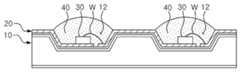
Translated fromKorean도 1은 본 발명의 일 실시예에 따른 백라이트용 LED 패키지를 도시한 단면도.1 is a cross-sectional view showing an LED package for a backlight according to an embodiment of the present invention.
도 2의 (a), (b) 및 (c)는 본 발명의 다른 실시예들에 따라 다양한 종류의 투광부재를 광 경로에 포함하는 LED 패키지를 도시한 단면도들.2A, 2B, and 3C are cross-sectional views illustrating LED packages including various types of light transmitting members in a light path according to other embodiments of the present invention.
도 3은 본 발명의 다른 실시예에 따라 투광부재가 생략되어 있는 LED 패키지를 도시한 단면도.3 is a cross-sectional view showing an LED package in which the light transmitting member is omitted in accordance with another embodiment of the present invention.
도 4는 본 발명의 다른 실시예에 따라 면광원을 제공하는 구조의 백라이트용 LED 패키지를 도시한 단면도.Figure 4 is a cross-sectional view showing an LED package for a backlight structure of providing a surface light source according to another embodiment of the present invention.
도 5는 본 발명의 또 다른 실시예에 따라 LED칩들이 투광부재의 측면에 인 접해 있는 백라이트용 LED 패키지를 도시한 단면도이다.FIG. 5 is a cross-sectional view illustrating a LED package for a backlight in which LED chips are adjacent to side surfaces of a light transmitting member according to another embodiment of the present invention.
<도면의 주요부분에 대한 부호설명><Code Description of Main Parts of Drawing>
10: 마운트기판 12: 홈10: mount substrate 12: groove
102: 베이스 기판 104: 투명 절연층102: base substrate 104: transparent insulating layer
106: 반사층 20: 도전성패턴층106: reflective layer 20: conductive pattern layer
22: 제 1 패턴전극 24: 제 2 패턴전극22: first pattern electrode 24: second pattern electrode
30: LED칩 40: 봉지재30: LED chip 40: encapsulant
50: 투광부재 52, 54: 프리즘패턴50:
본 발명은 LED 패키지에 관한 것으로서, 더욱 상세하게는, 마운트기판에 형성된 복수의 홈들 내에 수용된 복수의 LED칩들에 의해 확장된 광원을 제공할 수 있는 백라이트용 LED 패키지에 관한 것이다.The present invention relates to an LED package, and more particularly, to a LED package for a backlight that can provide a light source extended by a plurality of LED chips accommodated in a plurality of grooves formed in the mount substrate.
일반적으로, LED(Light Emitting Diode)는 전류 인가에 의한 p-n 반도체 접합(p-n junction)에 의해 전자와 정공이 만나 광을 발하는 소자로서, 통상, LED칩이 탑재된 패키지의 구조로 제작된다. LED칩이 실장된 채 패키지 구조로 제조된 발광 소자는 흔히, 'LED 패키지'라고 칭해지고 있다. 그리고, 그러한 LED 패키지는 외부로부터 전류를 인가받아 발광 동작하도록 구성된다.In general, an LED (Light Emitting Diode) is a device in which electrons and holes meet and emit light by a p-n semiconductor junction (p-n junction) by applying a current, and is generally manufactured in a package structure in which an LED chip is mounted. A light emitting device manufactured in a package structure with an LED chip mounted thereon is often referred to as an 'LED package'. In addition, such an LED package is configured to emit light by receiving a current from the outside.
위와 같은 LED 패키지는 LCD(Liquid Crystal Display)와 같은 디스플레이 장치의 백라이트 광원으로 이용될 수 있다. 그리고, LED 패키지는, 조명 객체에 백라이트 광원을 제공하는 방향에 따라, 수직 방향으로 광원을 제공하는 직상형과 측면 방향으로 광원을 제공하는 측면형 LED 패키지로 분류될 수 있다.The LED package may be used as a backlight light source of a display device such as an LCD (Liquid Crystal Display). The LED package may be classified into a direct type providing a light source in a vertical direction and a side type LED package providing a light source in a lateral direction according to a direction of providing a backlight light source to the lighting object.
통상, 하나의 LED 패키지는, 조명 객체에 대해 점광원을 제공하므로, 조명 객체 전반을 조명하는 것이 어렵다. 이에 따라, 선광원 또는 면광원의 제공을 위해서는, 복수의 LED 패키지들을 이용하는 것이 일반적이다. 그러나, 하나의 백라이트 광원 제공을 위해, 여러 부품으로 이루어진 복수의 LED 패키지를 이용하는 것은 경 제적이지 못하다는 문제점이 있다. 또한, 각각이 점광원인 복수의 LED 패키지를 선광원 또는 면광원을 제공하도록 정확하게 배열하는 것은 어려웠고 그 배열 공정 또한 번거롭다 복잡하다.Typically, one LED package provides a point light source for the illumination object, so it is difficult to illuminate the entire illumination object. Accordingly, in order to provide a linear light source or a surface light source, it is common to use a plurality of LED packages. However, there is a problem that it is not economical to use a plurality of LED packages composed of several components to provide one backlight light source. In addition, it is difficult to accurately arrange a plurality of LED packages, each of which is a point light source, to provide a line light source or a surface light source, and the arrangement process is cumbersome and complicated.
당해 기술분야에서는, 선광원 또는 면광원과 같이 확장된 백라이트 광원을 제공할 수 있는 단일 LED 패키지에 대한 요구가 있다. 이에 대해, 본 출원인은, 마운트기판 상에 LED칩이 실장되는 종래 LED 패키지를 개선하여, 확장된 백라이트 광원을 얻을 수 있는 백라이트용 LED 패키지를 개발하게 되었다.There is a need in the art for a single LED package that can provide an extended backlight light source, such as a linear or surface light source. On the other hand, the present applicant has improved the conventional LED package in which the LED chip is mounted on the mount substrate, thereby developing a LED package for backlight which can obtain an extended backlight light source.
본 발명은, 마운트기판에 형성된 복수의 홈들 내에 수용된 복수의 LED칩들에 의해, 확장된 백라이트 광원을 얻는 구조의 백라이트용 LED 패키지를 제공하는데 그 기술적 과제가 있다.The present invention provides a backlight LED package having a structure in which an extended backlight light source is obtained by a plurality of LED chips accommodated in a plurality of grooves formed in a mount substrate.
전술한 기술적 과제를 달성하기 위해, 본 발명에 따른 백라이트용 LED 패키지는, 복수의 홈들을 상부면에 갖는 마운트기판과; 상기 마운트기판의 상부면에 형성되며, 상기 홈들 각각의 내부에서 서로 이격된 제 1 및 제 2 패턴전극을 갖는 도전성패턴층과; 상기 홈들 내에 수용되며, 상기 제 1 패턴전극에 실장되고 상기 제 2 패턴전극과 전기 배선되는 복수의 LED칩들을 포함하되, 상기 제 1 패턴전극과 상기 제 2 패턴전극은 서로 이웃하는 상기 홈들 사이에서 연결되어, 상기 복수의 LED칩들을 직렬로 연결하도록 구성된다. 이때, 상기 마운트기판은, 복수의 홈들이 형성된 베이스 기판 상에 반사층과 투명 절연층이 차례로 적층 형성되어 이루어진 것이 바람직하다. 이때, 상기 베이스 기판은 실리콘 기판 또는 사파이어 기판인 것이 바람직하다. 그리고, 상기 베이스 기판은 실리콘 기판 또는 사파이어 기판으로부터 선택되며, 홈은 기판 두께, 베이스 기판의 두께보다 작은 깊이로 형성된다.In order to achieve the above technical problem, the LED package for a backlight according to the present invention, the mounting substrate having a plurality of grooves on the upper surface; A conductive pattern layer formed on an upper surface of the mount substrate and having first and second pattern electrodes spaced apart from each other in each of the grooves; And a plurality of LED chips accommodated in the grooves and mounted on the first pattern electrode and electrically connected to the second pattern electrode, wherein the first pattern electrode and the second pattern electrode are adjacent to each other between the grooves. Connected to the plurality of LED chips in series. In this case, the mount substrate is preferably formed by laminating a reflective layer and a transparent insulating layer on a base substrate on which a plurality of grooves are formed. In this case, the base substrate is preferably a silicon substrate or a sapphire substrate. The base substrate is selected from a silicon substrate or a sapphire substrate, and the groove is formed to a depth smaller than the thickness of the substrate and the thickness of the base substrate.
바람직하게는, 상기 백라이트용 LED 패키지는, 상기 도전성 패턴층이 형성된 상기 마운트기판의 상부면에 부착되어 상기 홈들 내의 LED칩들을 덮는 투광부재를 더 포함한다. 상기 투광부재의 상부면과 하부면 중 적어도 한 면에는 프리즘패턴이 형성된 것이 바람직하다. 더욱 바람직하게는, 상기 프리즘패턴은 상측으로의 광 방향성을 높이는 패턴 또는 광을 확산시키는 패턴일 수 있다. 또한, 상기 투광부재는 상기 여러 개소들에서 솔더링에 의해 부착될 수 있다.Preferably, the backlight LED package further includes a light transmitting member attached to an upper surface of the mount substrate on which the conductive pattern layer is formed to cover the LED chips in the grooves. It is preferable that a prism pattern is formed on at least one of an upper surface and a lower surface of the light transmitting member. More preferably, the prism pattern may be a pattern for increasing light direction to the upper side or a pattern for diffusing light. In addition, the light transmitting member may be attached by soldering at the various places.
바람직하게는, 상기 백라이트용 LED 패키지는, 상기 홈들 각각 내에 충전되어 형성된 투광성 봉지재들을 더 포함한다.Preferably, the LED package for backlight further comprises a transparent encapsulant formed in each of the grooves.
한편, 전술한 투광부재는 도광판인 것이 바람직하며, 상기 복수의 홈들 내에 위치한 LED칩들 각각은 상기 도광판의 측면에 인접해 있다. 또한, 상기 투광부재의 광입사면과 광출사면들 중 적어도 하나의 면에는 색 변환물질이 도포되어 있는 것이 바람직하다.
본 발명의 다른 측면에 따라, 도광판과 복수의 LDED칩들이 상기 도광판의 측면에 인접해 있는 하나의 LED 패키지를 포함하는 백라이트 유닛이 제공되며, 상기 백라이트 유닛의 LED 패키지는, 상부면에 복수의 홈들을 갖는 마운트기판과; 상기 마운트기판의 상부면에 형성되며, 상기 홈들 각각의 내부에서 서로 이격된 제 1 및 제 2 패턴전극을 갖는 도전성패턴층과; 상기 홈들 내에 수용되며, 상기 제 1 패턴전극에 실장되고 상기 제 2 패턴전극과 전기 배선되는 복수의 LED칩들을 포함하되,상기 제 1 패턴전극과 상기 제 2 패턴전극은 서로 이웃하는 상기 홈들 사이에서 연결되어, 상기 복수의 LED칩들을 직렬로 연결하며, 상기 마운트기판은, 기판 두께보다 작은 깊이로 복수의 홈들이 형성된 베이스 기판 상에 금속 반사층과 투명 절연층이 차례로 적층 형성되어 이루어지며, 상기 베이스 기판은 사파이어 기판과 실리콘 기판 중 어느 하나로부터 선택된다.On the other hand, the above-mentioned light transmitting member is preferably a light guide plate, each of the LED chips located in the plurality of grooves are adjacent to the side of the light guide plate. In addition, at least one of the light incident surface and the light exit surface of the light transmitting member is preferably coated with a color conversion material.
According to another aspect of the present invention, there is provided a backlight unit including a light guide plate and one LED package in which a plurality of LDED chips are adjacent to a side of the light guide plate, wherein the LED package of the backlight unit has a plurality of grooves on an upper surface thereof. A mount substrate having a frame; A conductive pattern layer formed on an upper surface of the mount substrate and having first and second pattern electrodes spaced apart from each other in each of the grooves; And a plurality of LED chips accommodated in the grooves and mounted on the first pattern electrode and electrically wired to the second pattern electrode, wherein the first pattern electrode and the second pattern electrode are adjacent to each other between the grooves. Are connected to connect the plurality of LED chips in series, and the mount substrate is formed by sequentially laminating a metal reflective layer and a transparent insulating layer on a base substrate on which a plurality of grooves are formed to a depth smaller than a substrate thickness. The substrate is selected from either a sapphire substrate or a silicon substrate.
이하, 첨부된 도면들을 참조하여 본 발명의 실시예들을 상세히 설명하기로 한다. 다음에 소개되는 실시예들은 당업자에게 본 발명의 사상이 충분히 전달될 수 있도록 하기 위해 예로서 제공되는 것이다. 따라서, 본 발명은 이하 설명되는 실시예들에 한정되지 않고 다른 형태로 구체화될 수도 있다. 그리고, 도면들에 있어서, 구성요소의 폭, 길이, 두께 등은 편의를 위하여 과장되어 표현될 수 있다. 명세서 전체에 걸쳐서 동일한 참조번호들은 동일한 구성요소들을 나타낸다.Hereinafter, embodiments of the present invention will be described in detail with reference to the accompanying drawings. The following embodiments are provided as examples to ensure that the spirit of the present invention can be fully conveyed to those skilled in the art. Accordingly, the present invention is not limited to the embodiments described below and may be embodied in other forms. And, in the drawings, the width, length, thickness, etc. of the components may be exaggerated for convenience. Like numbers refer to like elements throughout.
도 1은 본 발명의 일 실시예에 따른 LED 패키지를 도시한 단면도이다. 도 1에 도시된 LED 패키지(1)는 선광원 또는 면광원과 같은 확장 광원을 제공하는 백라이트용 LED 패키지로서, 이하에서는 그 구조에 대한 보다 구체적인 설명이 이루어진다.1 is a cross-sectional view showing an LED package according to an embodiment of the present invention. The
도 1을 참조하면, 상기 LED 패키지(1)는, 마운트기판(10), 도전성패턴층(20), 그리고, 복수의 LED칩(30)을 포함한다. 상기 마운트기판(10)은 복수의 홈(12)들을 포함하는 것이고, 상기 복수의 LED칩(30)은 상기 홈(12)들 각각에 수용되는 것들이며, 상기 도전성패턴층(20)은 상기 LED칩(30)들에 전류를 인가하기 위해 형성된 것이다.Referring to FIG. 1, the
본 실시예에서, 상기 마운트기판(10)은, 예를 들면, 실리콘 기판 또는 사파이어 기판 등과 같은 베이스 기판(102) 상에 금속 반사층(104)과 투명 절연층(106)이 차례대로 적층 형성된 것이다. 상기 베이스 기판(102)의 상부면에는 복수의 홈(12)들이 미리 형성되고, 상기 금속 반사층(104)과 투명 절연층(106)은 상기 홈(12)들이 형성되어 있는 베이스 기판(102) 상에 차례대로 형성되는 것들이다. 상기 투명 절연층(106)이 투명 소재로 이루어지므로, 광은 투명 절연층(106)을 거쳐 그 아래에 위치한 금속 반사층(104)에 도달한 후 금속 반사층(104)에 의해 상측으로 반사된다.In the present exemplary embodiment, the
본 실시예에서, 베이스 기판(102), 금속 반사층(104) 및 투명 절연층(106)이 하나의 마운트기판(10)을 이루므로, 이하 실시예의 설명에서, 상기 투명 절연층(106) 상에 형성되는 것들은 마운트기판(10) 상에 형성되는 것과 동일한 것으로 정의한다.In the present embodiment, since the
상기 도전성패턴층(20)은 제 1 패턴전극(22)과 제 2 패턴전극(24)을 포함하며, 인쇄기법을 이용하여 상기 마운트기판(10) 상에 형성될 수 있다. 그리고, 상기 도전성패턴층(20)은 금속 도금 또는 금속 증착 또는 기타 다른 금속 코팅 방식에 의해 상기 마운트기판(10) 상에 형성될 수 있다.The
상기 마운트기판(10)에 형성된 복수의 홈(12)들 각각의 내부에서, 상기 제 1 패턴전극(22)과 상기 제 2 패턴전극(24)은 서로 이격되어 있다. 그리고, 상기 홈(12)들 외부에서, 더욱 구체적으로는, 서로 이웃하는 두 홈(12, 12)들 사이에서, 상기 제 1 패턴전극(22)과 상기 제 2 패턴전극(24)은 서로 연결되어 있다. 상기 복수의 홈(12)들에 수용된 복수의 LED칩(30)들 각각은, 상기 홈(12)들 내에서 상기 제 1 패턴전극(22)에 실장된다. 상기 LED칩(30)들 각각은 동일 홈(12) 내에 위치한 제 2 패턴전극(24)과 본딩와이어(W)에 의해 전기 배선된다. 도시되어 있지는 않지만, 홈(12) 외측에 위치한 제 1 전극패턴(22)과 제 2 전극패턴(24) 각각은 외부 전원과 전기적으로 연결된다. In each of the plurality of
이웃하는 두 홈(12, 12)들 사이에서 제 1 패턴전극(22)과 제 2 패턴전극(24)이 서로 연결되고, 홈(12)들 내부에서 각 LED칩(30)이 제 1 패턴전극(22)에 실장된 채 제 2 패턴전극(24)과 전기 배선되는 전술한 LED 패키지의 구조에 의해, 상기 복수의 LED칩(30)들은 전기적으로 직렬 연결될 수 있다. 그리고, 점광원들을 제공하는 LED칩(30)들 각각이 모여 하나의 확장된 광원인 선광원 또는 면광원을 제공할 수 있는 것이다.The
홈(12)들 각각에 수용된 LED칩(30)들로부터 후방으로 방출되는 광들은 마운트기판(10)의 투명 절연층(106) 아래에 위치한 반사층(104)에 의해 큰 광손실 없이 상측으로 반사될 수 있다. 그리고, 상기 반사층(104)이 상기 홈(12)들 내에서 각 LED칩(30) 주변을 둘러싸는 구조를 이루며, 이는 LED칩(30)들로부터 나온 광들이 보다 용이하게 혼합되어 보다 균일한 확장 광원을 제공하는데 기여한다.Light emitted backwards from the LED chips 30 accommodated in each of the
상기 홈(12)들 내에는 예를 들면, 에폭시 또는 실리콘 수지와 같은 투광성 수지가 충전되어 형성된 봉지재(40)들이 마련될 수 있다. 상기 봉지재(40)들은 홈(12)들 내에 수용되어 상기 LED칩(30)들을 보호하는 역할과 렌즈로서의 역할을 할 수 있다. 또한, 상기 봉지재(40)들에는 광에 의해 여기되어 다른 파장의 광을 생성하는 형광체(또는, 색변환물질)가 함유될 수 있다. 이때, 수지로 이루어진 봉지재(40) 대신에 유리와 같은 재질의 렌즈부재가 상기 홈(12) 상단에 설치되는 것도 가능하다. 이때, 상기 봉지재(40) 또는 렌즈부재는 광의 지향각을 조절할 수 있는 형상으로 형성되는 것이 바람직하다.In the
한편, 상기 LED 패키지(1)는 상기 도전성패턴층(20)이 형성된 상기 마운트기판(10)에 부착되어 상기 홈(12)들 내에 수용된 상기 LED칩(30)들을 전체적으로 덮는 대략 판상의 투광부재(50)를 포함한다. 상기 투광부재(50)는 그 아래쪽에 위치한 LED 패키지(1)의 여러 부품들을 전체적으로 보호하는 역할과 함께 LED칩(30)들로부터 나온 광을 백라이트 광원에 적합한 광이 되도록 조절하는 역할을 한다. 본 실시예에서, 상기 투광부재(50)는 홈(12)들 외측의 여러 개소들에 마련된 솔더링 범프(501)에 의해 상기 마운트기판(10) 또는 그 위의 도전성패턴층(20)에 솔더링 방식으로 부착될 수 있다.The
본 실시예에서, 상기 투광부재(50)의 하부면 및 상부면 각각에는 제 1 및 제 2 프리즘패턴(52, 54)이 형성된다. 상기 제 1 및 제 2 프리즘패턴(52, 54)은 상측으로의 광 방향성(또는, 직진성)을 높이는 패턴이거나 또는 광을 확산시키는 패턴일 수 있다. 그리고, 상기 투광부재(50)는 LED 패키지와 함께 백라이트 광원에 반드시 요구되었던 도광판 및/또는 확산시트의 생략을 가능하게 해줄 수 있다. 이때, 제 1 프리즘패턴(52)과 제 2 프리즘패턴(54)의 배향이 직각을 이루거나 교차되는 경우, 투광부재(50)의 광의 방향성을 높이거나 광을 산란시키는 성능이 보다 향상될 수 있다.In the present embodiment, first and
위 실시예에서는, 상기 투광부재(50)의 상부면과 하부면 모두에 프리즘패턴(52, 54)들이 형성되지만, 도 2의 (a), (b) 및 (C)에 도시된 것과 같이, 투광부재(50) 하부면에만 프리즘패턴(52)을 형성하거나(도 2의 (a)), 투광부재(50) 상부면에만 프리즘패턴(54)을 형성하거나(도 2의 (b)), 투광부재(50)의 상, 하 양면 모두에서 프리즘패턴을 생략할 수도 있다(도 2의 (c)). 또한, 도 3에 도시된 것과 같이, 투광부재(50)를 생략하고, 봉지재(40)의 렌즈 형상 조절에 의해, 원하는 백라이트 광원을 얻는 것도 고려될 수 있다. 하지만, 균일한 선광원 또는 면광원을 얻기 위해서는, 투광부재(50)가 설치된 LED 패키지(1) 바람직하다. 도면에서, 상기 홈(12)들 내에는 봉지재(40)들이 형성되지만, 상기 투광부재(50)가 봉지재(40)들의 역할을 대신할 수도 있다.In the above embodiment, the
본 발명에 따른 LED 패키지(1)는 마운트기판(10) 상에 일열로 형성된 홈(12) 들 내에 LED칩(30)들이 위치되는 구조 또는 마운트기판(10) 상에 2열 이상으로 형성된 홈(12)들 내에 LED칩(30)들이 위치된 구조일 수 있다. 전자(前者)의 경우, 선광원을 얻는데 적합하며, 후자(後者)의 경우, 면광원을 얻는데 적합하다.The
도 4는 면광원을 얻는데 적합한 2열 이상의 홈들 및 그 홈들에 수용된 LED칩들을 포함하는 LED 패키지의 평면도이다. 도 4에서 봉지재(40)와 투광부재(50) 등의 구성요소는 도시의 편의를 위해 생략되었다.4 is a plan view of an LED package including two or more rows of grooves suitable for obtaining a surface light source and LED chips received in the grooves. In FIG. 4, components such as the
도 4에 도시된 것과 같이, 본 실시예의 LED 패키지(1)는 마운트기판(10)의 상면에 2행 2열로 배열된 4개의 홈(12)들이 형성된다. 그리고, 상기 마운트기판(10) 상에는 제 1 및 제 2 패턴전극(22, 24)을 포함한 채 전체적으로 "ㄷ"형의 패턴을 갖고 형성된 도전성패턴층(20)이 마련된다. 상기 4개의 홈(12)들 각각의 내부에는 상기 제 1 패턴전극(22)과 제 2 전극패턴(24)이 서로 이격된 채 위치하며, 서로 이웃하는 홈(12)들 사이에서 제 1 패턴전극(22)과 제 2 패턴전극(24)은 서로 연결되어 있다. 이때, 상기 제 1 및 제 2 패턴전극(22, 24)들은, 상기 2행 2열의 홈(12) 및 LED칩(30) 배열에 상응하게, 서로 횡으로 연결되는 부분과 서로 종으로 연결되는 부분을 포함한다.As shown in FIG. 4, the
도 5는 본 발명의 또 다른 실시예에 따른 LED 패키지(1)을 도시한다. 도 5를 참조하면, 투광부재(50)가 도광판의 구조 및 기능을 가지며, 마운트기판(10)의 홈들(12)들에 형성된 복수의 LED칩(30)들 각각은 투광부재(50), 즉 도광판의 측면에 인접해 있다. 일반적으로, 도광판은 LED 패키지와 별도의 구성요소로 알려져 있지만, 본 명세서에서는, 도광판 역할을 하는 투광부재(50)이 LED 패키지(1)의 한 구 성요소인 것으로 정의한다. 이때, LED칩(30)과 인접해 있는 상기 투광부재(50)의 측면이 광입사면이 되고, 그와 수직을 이루는 넓은 면이 광출사면이 된다. 상기 광입사면 또는 광출사면은 형광체와 같은 색변환물질이 도포되어 형성되는 것이 바람직하다. 또한, 상기 투광부재(50)의 측면은 복수의 솔더링 범프(501)에 의해 마운트 기판(10)의 상부면에 부착된다.5 shows an
위의 여러 실시예들을 통해 설명된 본 발명에 따른 백라이트용 LED 패키지는, 다수의 LED칩(30)들이 각각 수용된 다수의 홈(12)들을 포함하고 그 LED칩(30)들에 전류를 인가하기 위한 도전성패턴층(20)이 형성된 마운트기판(10)을 복수개로 절단하여 이루어지되, 그 절단된 마운트기판(10)의 홈(12)은 및 그 홈(12) 내에 수용된 LED칩(30)은 복수개로 이루어진다. 그리고, 복수의 LED칩(30)들은 앞에서 설명된 도전성패턴층(20)의 구조에 의해 직렬로 연결되어, 도전성패턴층(20)을 통해 복수의 LED칩(30)들에 전류가 인가될 때, 확장된 광원을 제공할 수 있게 된다.The LED package for a backlight according to the present invention described through the above various embodiments includes a plurality of
본 발명의 실시예에 의하면, 디스프플레이 장치에 백라이트 광원을 제공함에 있어서, 단일 LED 패키지로 선광원 또는 점광원과 같이 확장된 광원을 제공하는 것이 가능하며, 이는 종래기술의 문제점, 즉, 여러개의 LED 패키지들을 배열하여 선광원 도는 점광원을 제공하는데 따른 여러 번거로움 및 비용 손실을 줄여주는데 기여할 수 있다.According to an embodiment of the present invention, in providing a backlight light source to the display device, it is possible to provide an extended light source such as a line light source or a point light source in a single LED package, which is a problem of the prior art, that is, several By arranging the LED packages of LEDs, it can contribute to reducing the hassle and cost loss of providing source light or point light source.
Claims (12)
Translated fromKoreanPriority Applications (1)
| Application Number | Priority Date | Filing Date | Title |
|---|---|---|---|
| KR1020070057822AKR100869530B1 (en) | 2007-06-13 | 2007-06-13 | LED package for backlight and backlight unit including same |
Applications Claiming Priority (1)
| Application Number | Priority Date | Filing Date | Title |
|---|---|---|---|
| KR1020070057822AKR100869530B1 (en) | 2007-06-13 | 2007-06-13 | LED package for backlight and backlight unit including same |
Publications (1)
| Publication Number | Publication Date |
|---|---|
| KR100869530B1true KR100869530B1 (en) | 2008-11-19 |
Family
ID=40284493
Family Applications (1)
| Application Number | Title | Priority Date | Filing Date |
|---|---|---|---|
| KR1020070057822AExpired - Fee RelatedKR100869530B1 (en) | 2007-06-13 | 2007-06-13 | LED package for backlight and backlight unit including same |
Country Status (1)
| Country | Link |
|---|---|
| KR (1) | KR100869530B1 (en) |
Cited By (10)
| Publication number | Priority date | Publication date | Assignee | Title |
|---|---|---|---|---|
| KR100986571B1 (en) | 2010-02-04 | 2010-10-07 | 엘지이노텍 주식회사 | Package of light emitting device and method for fabricating the same |
| KR101028329B1 (en) | 2010-04-28 | 2011-04-12 | 엘지이노텍 주식회사 | Light emitting device package and its manufacturing method |
| KR20110078482A (en)* | 2009-12-31 | 2011-07-07 | 서울반도체 주식회사 | Multi chip LED package and its manufacturing method |
| KR101124254B1 (en) | 2010-02-22 | 2012-03-27 | (주)포인트엔지니어링 | Optical Element Device Substrate and the Optical Element Device thereby and fabricating method thereof |
| US8399904B2 (en) | 2010-08-09 | 2013-03-19 | Lg Innotek Co., Ltd. | Light emitting device and lighting system having the same |
| KR101384175B1 (en) | 2007-09-28 | 2014-04-18 | 삼성전자주식회사 | Backlight unit |
| US8931944B2 (en) | 2011-08-09 | 2015-01-13 | Samsung Display Co., Ltd. | Display apparatus and light source packages employed therein |
| KR101582509B1 (en) | 2015-08-04 | 2016-01-05 | 주식회사 반얀트리 | A Manufacturing Method For Back Light Unit Using Alignment Apparatus |
| CN111312741A (en)* | 2020-03-06 | 2020-06-19 | 佛山市国星半导体技术有限公司 | An integrated three-dimensional Micro LED and its manufacturing method |
| CN115224180A (en)* | 2022-07-22 | 2022-10-21 | 深圳康佳电子科技有限公司 | A MINI light panel backlight module |
Citations (3)
| Publication number | Priority date | Publication date | Assignee | Title |
|---|---|---|---|---|
| JPH0278102A (en)* | 1987-12-24 | 1990-03-19 | Mitsubishi Cable Ind Ltd | light emitting diode lighting equipment |
| US6715901B2 (en) | 2002-08-15 | 2004-04-06 | Shi-Hwa Huang | Image projector system having a light source that includes at least four light emitting diode modules |
| JP2006013426A (en)* | 2004-01-28 | 2006-01-12 | Kyocera Corp | Light emitting device and lighting apparatus |
- 2007
- 2007-06-13KRKR1020070057822Apatent/KR100869530B1/ennot_activeExpired - Fee Related
Patent Citations (3)
| Publication number | Priority date | Publication date | Assignee | Title |
|---|---|---|---|---|
| JPH0278102A (en)* | 1987-12-24 | 1990-03-19 | Mitsubishi Cable Ind Ltd | light emitting diode lighting equipment |
| US6715901B2 (en) | 2002-08-15 | 2004-04-06 | Shi-Hwa Huang | Image projector system having a light source that includes at least four light emitting diode modules |
| JP2006013426A (en)* | 2004-01-28 | 2006-01-12 | Kyocera Corp | Light emitting device and lighting apparatus |
Cited By (14)
| Publication number | Priority date | Publication date | Assignee | Title |
|---|---|---|---|---|
| KR101384175B1 (en) | 2007-09-28 | 2014-04-18 | 삼성전자주식회사 | Backlight unit |
| KR101644149B1 (en)* | 2009-12-31 | 2016-08-10 | 서울반도체 주식회사 | Multi-chip led package and method of manufacturing the same |
| KR20110078482A (en)* | 2009-12-31 | 2011-07-07 | 서울반도체 주식회사 | Multi chip LED package and its manufacturing method |
| KR100986571B1 (en) | 2010-02-04 | 2010-10-07 | 엘지이노텍 주식회사 | Package of light emitting device and method for fabricating the same |
| US8519418B2 (en) | 2010-02-04 | 2013-08-27 | Lg Innotek Co., Ltd. | Light emitting device package having dielectric pattern on reflective layer |
| KR101124254B1 (en) | 2010-02-22 | 2012-03-27 | (주)포인트엔지니어링 | Optical Element Device Substrate and the Optical Element Device thereby and fabricating method thereof |
| US8680552B2 (en) | 2010-04-28 | 2014-03-25 | Lg Innotek Co., Ltd. | Light emitting device package including light emitting diode, and lighting system having the same |
| KR101028329B1 (en) | 2010-04-28 | 2011-04-12 | 엘지이노텍 주식회사 | Light emitting device package and its manufacturing method |
| US8399904B2 (en) | 2010-08-09 | 2013-03-19 | Lg Innotek Co., Ltd. | Light emitting device and lighting system having the same |
| US8931944B2 (en) | 2011-08-09 | 2015-01-13 | Samsung Display Co., Ltd. | Display apparatus and light source packages employed therein |
| KR101582509B1 (en) | 2015-08-04 | 2016-01-05 | 주식회사 반얀트리 | A Manufacturing Method For Back Light Unit Using Alignment Apparatus |
| CN111312741A (en)* | 2020-03-06 | 2020-06-19 | 佛山市国星半导体技术有限公司 | An integrated three-dimensional Micro LED and its manufacturing method |
| CN111312741B (en)* | 2020-03-06 | 2024-05-17 | 佛山市国星半导体技术有限公司 | An integrated three-dimensional Micro LED and a manufacturing method thereof |
| CN115224180A (en)* | 2022-07-22 | 2022-10-21 | 深圳康佳电子科技有限公司 | A MINI light panel backlight module |
Similar Documents
| Publication | Publication Date | Title |
|---|---|---|
| KR100869530B1 (en) | LED package for backlight and backlight unit including same | |
| US7217004B2 (en) | Light emitting diode array module for providing backlight and backlight unit having the same | |
| KR100732267B1 (en) | Linear light source and production method therefor and surface emission device | |
| US9837392B2 (en) | LED lighting apparatus | |
| WO2012001938A1 (en) | Light emitting device, backlight unit, liquid crystal display device, and lighting device | |
| US20210200026A1 (en) | Light-emitting device and liquid crystal display device | |
| CN110970408B (en) | Light-emitting device | |
| CN112885943B (en) | Light emitting device and LED packaging | |
| KR20190139636A (en) | surface emitting micro LED module | |
| KR20200019514A (en) | Light emitting diode package and display device including the same | |
| KR101646262B1 (en) | Light emitting device package and light unit having the seme | |
| JP2009521802A (en) | LED light confinement element | |
| JP5851262B2 (en) | Linear light source device, surface light emitting device, and liquid crystal display device | |
| US11506933B2 (en) | Light-emitting module, method for manufacturing the same, and liquid-crystal display device | |
| CN110364608B (en) | Wafer-level linear light source light-emitting device | |
| JP2008277189A (en) | Linear light source device and manufacturing method thereof | |
| KR101827972B1 (en) | light emitting package and backlight module using the same | |
| KR102008286B1 (en) | Light emitting device and lighting unit using the same | |
| KR20120062512A (en) | Led pakage and array, lcd module having thereof | |
| KR20170052900A (en) | LIGHT-EMITTING apparatus WITH HIGH EFFICIENCY | |
| US10267489B2 (en) | Light-emitting apparatus | |
| KR102424364B1 (en) | Light emitting diode | |
| KR20190125076A (en) | flexible LED lighting apparatus | |
| KR20140064582A (en) | Side light emitting led package, lighting array module, and fabrication method therof | |
| JP7438326B2 (en) | Light emitting device, manufacturing method thereof, and planar light emitting device |
Legal Events
| Date | Code | Title | Description |
|---|---|---|---|
| A201 | Request for examination | ||
| PA0109 | Patent application | St.27 status event code:A-0-1-A10-A12-nap-PA0109 | |
| PA0201 | Request for examination | St.27 status event code:A-1-2-D10-D11-exm-PA0201 | |
| D13-X000 | Search requested | St.27 status event code:A-1-2-D10-D13-srh-X000 | |
| D14-X000 | Search report completed | St.27 status event code:A-1-2-D10-D14-srh-X000 | |
| E902 | Notification of reason for refusal | ||
| PE0902 | Notice of grounds for rejection | St.27 status event code:A-1-2-D10-D21-exm-PE0902 | |
| E13-X000 | Pre-grant limitation requested | St.27 status event code:A-2-3-E10-E13-lim-X000 | |
| P11-X000 | Amendment of application requested | St.27 status event code:A-2-2-P10-P11-nap-X000 | |
| P13-X000 | Application amended | St.27 status event code:A-2-2-P10-P13-nap-X000 | |
| E701 | Decision to grant or registration of patent right | ||
| PE0701 | Decision of registration | St.27 status event code:A-1-2-D10-D22-exm-PE0701 | |
| GRNT | Written decision to grant | ||
| PR0701 | Registration of establishment | St.27 status event code:A-2-4-F10-F11-exm-PR0701 | |
| PR1002 | Payment of registration fee | St.27 status event code:A-2-2-U10-U11-oth-PR1002 Fee payment year number:1 | |
| PG1601 | Publication of registration | St.27 status event code:A-4-4-Q10-Q13-nap-PG1601 | |
| P22-X000 | Classification modified | St.27 status event code:A-4-4-P10-P22-nap-X000 | |
| PR1001 | Payment of annual fee | St.27 status event code:A-4-4-U10-U11-oth-PR1001 Fee payment year number:4 | |
| FPAY | Annual fee payment | Payment date:20120917 Year of fee payment:5 | |
| PR1001 | Payment of annual fee | St.27 status event code:A-4-4-U10-U11-oth-PR1001 Fee payment year number:5 | |
| FPAY | Annual fee payment | Payment date:20130911 Year of fee payment:6 | |
| PR1001 | Payment of annual fee | St.27 status event code:A-4-4-U10-U11-oth-PR1001 Fee payment year number:6 | |
| FPAY | Annual fee payment | Payment date:20140912 Year of fee payment:7 | |
| PR1001 | Payment of annual fee | St.27 status event code:A-4-4-U10-U11-oth-PR1001 Fee payment year number:7 | |
| PN2301 | Change of applicant | St.27 status event code:A-5-5-R10-R13-asn-PN2301 St.27 status event code:A-5-5-R10-R11-asn-PN2301 | |
| FPAY | Annual fee payment | Payment date:20150902 Year of fee payment:8 | |
| PR1001 | Payment of annual fee | St.27 status event code:A-4-4-U10-U11-oth-PR1001 Fee payment year number:8 | |
| R18-X000 | Changes to party contact information recorded | St.27 status event code:A-5-5-R10-R18-oth-X000 | |
| FPAY | Annual fee payment | Payment date:20160907 Year of fee payment:9 | |
| PR1001 | Payment of annual fee | St.27 status event code:A-4-4-U10-U11-oth-PR1001 Fee payment year number:9 | |
| P22-X000 | Classification modified | St.27 status event code:A-4-4-P10-P22-nap-X000 | |
| PR1001 | Payment of annual fee | St.27 status event code:A-4-4-U10-U11-oth-PR1001 Fee payment year number:10 | |
| PR1001 | Payment of annual fee | St.27 status event code:A-4-4-U10-U11-oth-PR1001 Fee payment year number:11 | |
| PC1903 | Unpaid annual fee | St.27 status event code:A-4-4-U10-U13-oth-PC1903 Not in force date:20191114 Payment event data comment text:Termination Category : DEFAULT_OF_REGISTRATION_FEE | |
| PC1903 | Unpaid annual fee | St.27 status event code:N-4-6-H10-H13-oth-PC1903 Ip right cessation event data comment text:Termination Category : DEFAULT_OF_REGISTRATION_FEE Not in force date:20191114 | |
| P22-X000 | Classification modified | St.27 status event code:A-4-4-P10-P22-nap-X000 |