KR100868608B1 - Manufacturing method of semiconductor device - Google Patents
Manufacturing method of semiconductor deviceDownload PDFInfo
- Publication number
- KR100868608B1 KR100868608B1KR1020080059219AKR20080059219AKR100868608B1KR 100868608 B1KR100868608 B1KR 100868608B1KR 1020080059219 AKR1020080059219 AKR 1020080059219AKR 20080059219 AKR20080059219 AKR 20080059219AKR 100868608 B1KR100868608 B1KR 100868608B1
- Authority
- KR
- South Korea
- Prior art keywords
- semiconductor device
- substrate
- external electrode
- lead
- semiconductor element
- Prior art date
- Legal status (The legal status is an assumption and is not a legal conclusion. Google has not performed a legal analysis and makes no representation as to the accuracy of the status listed.)
- Expired - Fee Related
Links
Images


Classifications
- H—ELECTRICITY
- H01—ELECTRIC ELEMENTS
- H01L—SEMICONDUCTOR DEVICES NOT COVERED BY CLASS H10
- H01L24/00—Arrangements for connecting or disconnecting semiconductor or solid-state bodies; Methods or apparatus related thereto
- H01L24/01—Means for bonding being attached to, or being formed on, the surface to be connected, e.g. chip-to-package, die-attach, "first-level" interconnects; Manufacturing methods related thereto
- H01L24/26—Layer connectors, e.g. plate connectors, solder or adhesive layers; Manufacturing methods related thereto
- H01L24/31—Structure, shape, material or disposition of the layer connectors after the connecting process
- H01L24/32—Structure, shape, material or disposition of the layer connectors after the connecting process of an individual layer connector
- H—ELECTRICITY
- H01—ELECTRIC ELEMENTS
- H01L—SEMICONDUCTOR DEVICES NOT COVERED BY CLASS H10
- H01L23/00—Details of semiconductor or other solid state devices
- H01L23/28—Encapsulations, e.g. encapsulating layers, coatings, e.g. for protection
- H—ELECTRICITY
- H01—ELECTRIC ELEMENTS
- H01L—SEMICONDUCTOR DEVICES NOT COVERED BY CLASS H10
- H01L21/00—Processes or apparatus adapted for the manufacture or treatment of semiconductor or solid state devices or of parts thereof
- H01L21/02—Manufacture or treatment of semiconductor devices or of parts thereof
- H01L21/04—Manufacture or treatment of semiconductor devices or of parts thereof the devices having potential barriers, e.g. a PN junction, depletion layer or carrier concentration layer
- H01L21/48—Manufacture or treatment of parts, e.g. containers, prior to assembly of the devices, using processes not provided for in a single one of the groups H01L21/18 - H01L21/326 or H10D48/04 - H10D48/07
- H01L21/4814—Conductive parts
- H01L21/4821—Flat leads, e.g. lead frames with or without insulating supports
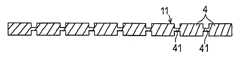
- H01L21/4828—Etching
- H01L21/4832—Etching a temporary substrate after encapsulation process to form leads
- H—ELECTRICITY
- H01—ELECTRIC ELEMENTS
- H01L—SEMICONDUCTOR DEVICES NOT COVERED BY CLASS H10
- H01L21/00—Processes or apparatus adapted for the manufacture or treatment of semiconductor or solid state devices or of parts thereof
- H01L21/02—Manufacture or treatment of semiconductor devices or of parts thereof
- H01L21/04—Manufacture or treatment of semiconductor devices or of parts thereof the devices having potential barriers, e.g. a PN junction, depletion layer or carrier concentration layer
- H01L21/50—Assembly of semiconductor devices using processes or apparatus not provided for in a single one of the groups H01L21/18 - H01L21/326 or H10D48/04 - H10D48/07 e.g. sealing of a cap to a base of a container
- H01L21/56—Encapsulations, e.g. encapsulation layers, coatings
- H01L21/561—Batch processing
- H—ELECTRICITY
- H01—ELECTRIC ELEMENTS
- H01L—SEMICONDUCTOR DEVICES NOT COVERED BY CLASS H10
- H01L23/00—Details of semiconductor or other solid state devices
- H01L23/28—Encapsulations, e.g. encapsulating layers, coatings, e.g. for protection
- H01L23/31—Encapsulations, e.g. encapsulating layers, coatings, e.g. for protection characterised by the arrangement or shape
- H01L23/3107—Encapsulations, e.g. encapsulating layers, coatings, e.g. for protection characterised by the arrangement or shape the device being completely enclosed
- H—ELECTRICITY
- H01—ELECTRIC ELEMENTS
- H01L—SEMICONDUCTOR DEVICES NOT COVERED BY CLASS H10
- H01L24/00—Arrangements for connecting or disconnecting semiconductor or solid-state bodies; Methods or apparatus related thereto
- H01L24/01—Means for bonding being attached to, or being formed on, the surface to be connected, e.g. chip-to-package, die-attach, "first-level" interconnects; Manufacturing methods related thereto
- H01L24/42—Wire connectors; Manufacturing methods related thereto
- H01L24/47—Structure, shape, material or disposition of the wire connectors after the connecting process
- H01L24/49—Structure, shape, material or disposition of the wire connectors after the connecting process of a plurality of wire connectors
- H—ELECTRICITY
- H01—ELECTRIC ELEMENTS
- H01L—SEMICONDUCTOR DEVICES NOT COVERED BY CLASS H10
- H01L24/00—Arrangements for connecting or disconnecting semiconductor or solid-state bodies; Methods or apparatus related thereto
- H01L24/93—Batch processes
- H01L24/95—Batch processes at chip-level, i.e. with connecting carried out on a plurality of singulated devices, i.e. on diced chips
- H01L24/97—Batch processes at chip-level, i.e. with connecting carried out on a plurality of singulated devices, i.e. on diced chips the devices being connected to a common substrate, e.g. interposer, said common substrate being separable into individual assemblies after connecting
- H—ELECTRICITY
- H01—ELECTRIC ELEMENTS
- H01L—SEMICONDUCTOR DEVICES NOT COVERED BY CLASS H10
- H01L2221/00—Processes or apparatus adapted for the manufacture or treatment of semiconductor or solid state devices or of parts thereof covered by H01L21/00
- H01L2221/67—Apparatus for handling semiconductor or electric solid state devices during manufacture or treatment thereof; Apparatus for handling wafers during manufacture or treatment of semiconductor or electric solid state devices or components; Apparatus not specifically provided for elsewhere
- H01L2221/683—Apparatus for handling semiconductor or electric solid state devices during manufacture or treatment thereof; Apparatus for handling wafers during manufacture or treatment of semiconductor or electric solid state devices or components; Apparatus not specifically provided for elsewhere for supporting or gripping
- H01L2221/68304—Apparatus for handling semiconductor or electric solid state devices during manufacture or treatment thereof; Apparatus for handling wafers during manufacture or treatment of semiconductor or electric solid state devices or components; Apparatus not specifically provided for elsewhere for supporting or gripping using temporarily an auxiliary support
- H01L2221/68377—Apparatus for handling semiconductor or electric solid state devices during manufacture or treatment thereof; Apparatus for handling wafers during manufacture or treatment of semiconductor or electric solid state devices or components; Apparatus not specifically provided for elsewhere for supporting or gripping using temporarily an auxiliary support with parts of the auxiliary support remaining in the finished device
- H—ELECTRICITY
- H01—ELECTRIC ELEMENTS
- H01L—SEMICONDUCTOR DEVICES NOT COVERED BY CLASS H10
- H01L2224/00—Indexing scheme for arrangements for connecting or disconnecting semiconductor or solid-state bodies and methods related thereto as covered by H01L24/00
- H01L2224/01—Means for bonding being attached to, or being formed on, the surface to be connected, e.g. chip-to-package, die-attach, "first-level" interconnects; Manufacturing methods related thereto
- H01L2224/02—Bonding areas; Manufacturing methods related thereto
- H01L2224/04—Structure, shape, material or disposition of the bonding areas prior to the connecting process
- H01L2224/05—Structure, shape, material or disposition of the bonding areas prior to the connecting process of an individual bonding area
- H01L2224/0554—External layer
- H01L2224/0555—Shape
- H01L2224/05552—Shape in top view
- H01L2224/05554—Shape in top view being square
- H—ELECTRICITY
- H01—ELECTRIC ELEMENTS
- H01L—SEMICONDUCTOR DEVICES NOT COVERED BY CLASS H10
- H01L2224/00—Indexing scheme for arrangements for connecting or disconnecting semiconductor or solid-state bodies and methods related thereto as covered by H01L24/00
- H01L2224/01—Means for bonding being attached to, or being formed on, the surface to be connected, e.g. chip-to-package, die-attach, "first-level" interconnects; Manufacturing methods related thereto
- H01L2224/26—Layer connectors, e.g. plate connectors, solder or adhesive layers; Manufacturing methods related thereto
- H01L2224/28—Structure, shape, material or disposition of the layer connectors prior to the connecting process
- H01L2224/29—Structure, shape, material or disposition of the layer connectors prior to the connecting process of an individual layer connector
- H01L2224/29001—Core members of the layer connector
- H01L2224/29005—Structure
- H01L2224/29007—Layer connector smaller than the underlying bonding area
- H—ELECTRICITY
- H01—ELECTRIC ELEMENTS
- H01L—SEMICONDUCTOR DEVICES NOT COVERED BY CLASS H10
- H01L2224/00—Indexing scheme for arrangements for connecting or disconnecting semiconductor or solid-state bodies and methods related thereto as covered by H01L24/00
- H01L2224/01—Means for bonding being attached to, or being formed on, the surface to be connected, e.g. chip-to-package, die-attach, "first-level" interconnects; Manufacturing methods related thereto
- H01L2224/26—Layer connectors, e.g. plate connectors, solder or adhesive layers; Manufacturing methods related thereto
- H01L2224/28—Structure, shape, material or disposition of the layer connectors prior to the connecting process
- H01L2224/29—Structure, shape, material or disposition of the layer connectors prior to the connecting process of an individual layer connector
- H01L2224/29001—Core members of the layer connector
- H01L2224/29099—Material
- H01L2224/291—Material with a principal constituent of the material being a metal or a metalloid, e.g. boron [B], silicon [Si], germanium [Ge], arsenic [As], antimony [Sb], tellurium [Te] and polonium [Po], and alloys thereof
- H01L2224/29101—Material with a principal constituent of the material being a metal or a metalloid, e.g. boron [B], silicon [Si], germanium [Ge], arsenic [As], antimony [Sb], tellurium [Te] and polonium [Po], and alloys thereof the principal constituent melting at a temperature of less than 400°C
- H01L2224/29111—Tin [Sn] as principal constituent
- H—ELECTRICITY
- H01—ELECTRIC ELEMENTS
- H01L—SEMICONDUCTOR DEVICES NOT COVERED BY CLASS H10
- H01L2224/00—Indexing scheme for arrangements for connecting or disconnecting semiconductor or solid-state bodies and methods related thereto as covered by H01L24/00
- H01L2224/01—Means for bonding being attached to, or being formed on, the surface to be connected, e.g. chip-to-package, die-attach, "first-level" interconnects; Manufacturing methods related thereto
- H01L2224/26—Layer connectors, e.g. plate connectors, solder or adhesive layers; Manufacturing methods related thereto
- H01L2224/28—Structure, shape, material or disposition of the layer connectors prior to the connecting process
- H01L2224/29—Structure, shape, material or disposition of the layer connectors prior to the connecting process of an individual layer connector
- H01L2224/29001—Core members of the layer connector
- H01L2224/29099—Material
- H01L2224/291—Material with a principal constituent of the material being a metal or a metalloid, e.g. boron [B], silicon [Si], germanium [Ge], arsenic [As], antimony [Sb], tellurium [Te] and polonium [Po], and alloys thereof
- H01L2224/29138—Material with a principal constituent of the material being a metal or a metalloid, e.g. boron [B], silicon [Si], germanium [Ge], arsenic [As], antimony [Sb], tellurium [Te] and polonium [Po], and alloys thereof the principal constituent melting at a temperature of greater than or equal to 950°C and less than 1550°C
- H01L2224/29139—Silver [Ag] as principal constituent
- H—ELECTRICITY
- H01—ELECTRIC ELEMENTS
- H01L—SEMICONDUCTOR DEVICES NOT COVERED BY CLASS H10
- H01L2224/00—Indexing scheme for arrangements for connecting or disconnecting semiconductor or solid-state bodies and methods related thereto as covered by H01L24/00
- H01L2224/01—Means for bonding being attached to, or being formed on, the surface to be connected, e.g. chip-to-package, die-attach, "first-level" interconnects; Manufacturing methods related thereto
- H01L2224/26—Layer connectors, e.g. plate connectors, solder or adhesive layers; Manufacturing methods related thereto
- H01L2224/31—Structure, shape, material or disposition of the layer connectors after the connecting process
- H01L2224/32—Structure, shape, material or disposition of the layer connectors after the connecting process of an individual layer connector
- H01L2224/3201—Structure
- H01L2224/32012—Structure relative to the bonding area, e.g. bond pad
- H01L2224/32014—Structure relative to the bonding area, e.g. bond pad the layer connector being smaller than the bonding area, e.g. bond pad
- H—ELECTRICITY
- H01—ELECTRIC ELEMENTS
- H01L—SEMICONDUCTOR DEVICES NOT COVERED BY CLASS H10
- H01L2224/00—Indexing scheme for arrangements for connecting or disconnecting semiconductor or solid-state bodies and methods related thereto as covered by H01L24/00
- H01L2224/01—Means for bonding being attached to, or being formed on, the surface to be connected, e.g. chip-to-package, die-attach, "first-level" interconnects; Manufacturing methods related thereto
- H01L2224/26—Layer connectors, e.g. plate connectors, solder or adhesive layers; Manufacturing methods related thereto
- H01L2224/31—Structure, shape, material or disposition of the layer connectors after the connecting process
- H01L2224/32—Structure, shape, material or disposition of the layer connectors after the connecting process of an individual layer connector
- H01L2224/321—Disposition
- H01L2224/32151—Disposition the layer connector connecting between a semiconductor or solid-state body and an item not being a semiconductor or solid-state body, e.g. chip-to-substrate, chip-to-passive
- H01L2224/32221—Disposition the layer connector connecting between a semiconductor or solid-state body and an item not being a semiconductor or solid-state body, e.g. chip-to-substrate, chip-to-passive the body and the item being stacked
- H01L2224/32245—Disposition the layer connector connecting between a semiconductor or solid-state body and an item not being a semiconductor or solid-state body, e.g. chip-to-substrate, chip-to-passive the body and the item being stacked the item being metallic
- H—ELECTRICITY
- H01—ELECTRIC ELEMENTS
- H01L—SEMICONDUCTOR DEVICES NOT COVERED BY CLASS H10
- H01L2224/00—Indexing scheme for arrangements for connecting or disconnecting semiconductor or solid-state bodies and methods related thereto as covered by H01L24/00
- H01L2224/01—Means for bonding being attached to, or being formed on, the surface to be connected, e.g. chip-to-package, die-attach, "first-level" interconnects; Manufacturing methods related thereto
- H01L2224/42—Wire connectors; Manufacturing methods related thereto
- H01L2224/44—Structure, shape, material or disposition of the wire connectors prior to the connecting process
- H01L2224/45—Structure, shape, material or disposition of the wire connectors prior to the connecting process of an individual wire connector
- H01L2224/45001—Core members of the connector
- H01L2224/45099—Material
- H01L2224/451—Material with a principal constituent of the material being a metal or a metalloid, e.g. boron (B), silicon (Si), germanium (Ge), arsenic (As), antimony (Sb), tellurium (Te) and polonium (Po), and alloys thereof
- H01L2224/45138—Material with a principal constituent of the material being a metal or a metalloid, e.g. boron (B), silicon (Si), germanium (Ge), arsenic (As), antimony (Sb), tellurium (Te) and polonium (Po), and alloys thereof the principal constituent melting at a temperature of greater than or equal to 950°C and less than 1550°C
- H01L2224/45144—Gold (Au) as principal constituent
- H—ELECTRICITY
- H01—ELECTRIC ELEMENTS
- H01L—SEMICONDUCTOR DEVICES NOT COVERED BY CLASS H10
- H01L2224/00—Indexing scheme for arrangements for connecting or disconnecting semiconductor or solid-state bodies and methods related thereto as covered by H01L24/00
- H01L2224/01—Means for bonding being attached to, or being formed on, the surface to be connected, e.g. chip-to-package, die-attach, "first-level" interconnects; Manufacturing methods related thereto
- H01L2224/42—Wire connectors; Manufacturing methods related thereto
- H01L2224/47—Structure, shape, material or disposition of the wire connectors after the connecting process
- H01L2224/48—Structure, shape, material or disposition of the wire connectors after the connecting process of an individual wire connector
- H01L2224/4805—Shape
- H01L2224/4809—Loop shape
- H01L2224/48091—Arched
- H—ELECTRICITY
- H01—ELECTRIC ELEMENTS
- H01L—SEMICONDUCTOR DEVICES NOT COVERED BY CLASS H10
- H01L2224/00—Indexing scheme for arrangements for connecting or disconnecting semiconductor or solid-state bodies and methods related thereto as covered by H01L24/00
- H01L2224/01—Means for bonding being attached to, or being formed on, the surface to be connected, e.g. chip-to-package, die-attach, "first-level" interconnects; Manufacturing methods related thereto
- H01L2224/42—Wire connectors; Manufacturing methods related thereto
- H01L2224/47—Structure, shape, material or disposition of the wire connectors after the connecting process
- H01L2224/48—Structure, shape, material or disposition of the wire connectors after the connecting process of an individual wire connector
- H01L2224/481—Disposition
- H01L2224/48151—Connecting between a semiconductor or solid-state body and an item not being a semiconductor or solid-state body, e.g. chip-to-substrate, chip-to-passive
- H01L2224/48221—Connecting between a semiconductor or solid-state body and an item not being a semiconductor or solid-state body, e.g. chip-to-substrate, chip-to-passive the body and the item being stacked
- H01L2224/48245—Connecting between a semiconductor or solid-state body and an item not being a semiconductor or solid-state body, e.g. chip-to-substrate, chip-to-passive the body and the item being stacked the item being metallic
- H01L2224/48247—Connecting between a semiconductor or solid-state body and an item not being a semiconductor or solid-state body, e.g. chip-to-substrate, chip-to-passive the body and the item being stacked the item being metallic connecting the wire to a bond pad of the item
- H—ELECTRICITY
- H01—ELECTRIC ELEMENTS
- H01L—SEMICONDUCTOR DEVICES NOT COVERED BY CLASS H10
- H01L2224/00—Indexing scheme for arrangements for connecting or disconnecting semiconductor or solid-state bodies and methods related thereto as covered by H01L24/00
- H01L2224/01—Means for bonding being attached to, or being formed on, the surface to be connected, e.g. chip-to-package, die-attach, "first-level" interconnects; Manufacturing methods related thereto
- H01L2224/42—Wire connectors; Manufacturing methods related thereto
- H01L2224/47—Structure, shape, material or disposition of the wire connectors after the connecting process
- H01L2224/48—Structure, shape, material or disposition of the wire connectors after the connecting process of an individual wire connector
- H01L2224/481—Disposition
- H01L2224/48151—Connecting between a semiconductor or solid-state body and an item not being a semiconductor or solid-state body, e.g. chip-to-substrate, chip-to-passive
- H01L2224/48221—Connecting between a semiconductor or solid-state body and an item not being a semiconductor or solid-state body, e.g. chip-to-substrate, chip-to-passive the body and the item being stacked
- H01L2224/48245—Connecting between a semiconductor or solid-state body and an item not being a semiconductor or solid-state body, e.g. chip-to-substrate, chip-to-passive the body and the item being stacked the item being metallic
- H01L2224/48257—Connecting between a semiconductor or solid-state body and an item not being a semiconductor or solid-state body, e.g. chip-to-substrate, chip-to-passive the body and the item being stacked the item being metallic connecting the wire to a die pad of the item
- H—ELECTRICITY
- H01—ELECTRIC ELEMENTS
- H01L—SEMICONDUCTOR DEVICES NOT COVERED BY CLASS H10
- H01L2224/00—Indexing scheme for arrangements for connecting or disconnecting semiconductor or solid-state bodies and methods related thereto as covered by H01L24/00
- H01L2224/01—Means for bonding being attached to, or being formed on, the surface to be connected, e.g. chip-to-package, die-attach, "first-level" interconnects; Manufacturing methods related thereto
- H01L2224/42—Wire connectors; Manufacturing methods related thereto
- H01L2224/47—Structure, shape, material or disposition of the wire connectors after the connecting process
- H01L2224/48—Structure, shape, material or disposition of the wire connectors after the connecting process of an individual wire connector
- H01L2224/485—Material
- H01L2224/48505—Material at the bonding interface
- H01L2224/48599—Principal constituent of the connecting portion of the wire connector being Gold (Au)
- H01L2224/486—Principal constituent of the connecting portion of the wire connector being Gold (Au) with a principal constituent of the bonding area being a metal or a metalloid, e.g. boron (B), silicon (Si), germanium (Ge), arsenic (As), antimony (Sb), tellurium (Te) and polonium (Po), and alloys thereof
- H01L2224/48638—Principal constituent of the connecting portion of the wire connector being Gold (Au) with a principal constituent of the bonding area being a metal or a metalloid, e.g. boron (B), silicon (Si), germanium (Ge), arsenic (As), antimony (Sb), tellurium (Te) and polonium (Po), and alloys thereof the principal constituent melting at a temperature of greater than or equal to 950°C and less than 1550°C
- H01L2224/48639—Silver (Ag) as principal constituent
- H—ELECTRICITY
- H01—ELECTRIC ELEMENTS
- H01L—SEMICONDUCTOR DEVICES NOT COVERED BY CLASS H10
- H01L2224/00—Indexing scheme for arrangements for connecting or disconnecting semiconductor or solid-state bodies and methods related thereto as covered by H01L24/00
- H01L2224/01—Means for bonding being attached to, or being formed on, the surface to be connected, e.g. chip-to-package, die-attach, "first-level" interconnects; Manufacturing methods related thereto
- H01L2224/42—Wire connectors; Manufacturing methods related thereto
- H01L2224/47—Structure, shape, material or disposition of the wire connectors after the connecting process
- H01L2224/48—Structure, shape, material or disposition of the wire connectors after the connecting process of an individual wire connector
- H01L2224/485—Material
- H01L2224/48505—Material at the bonding interface
- H01L2224/48599—Principal constituent of the connecting portion of the wire connector being Gold (Au)
- H01L2224/486—Principal constituent of the connecting portion of the wire connector being Gold (Au) with a principal constituent of the bonding area being a metal or a metalloid, e.g. boron (B), silicon (Si), germanium (Ge), arsenic (As), antimony (Sb), tellurium (Te) and polonium (Po), and alloys thereof
- H01L2224/48638—Principal constituent of the connecting portion of the wire connector being Gold (Au) with a principal constituent of the bonding area being a metal or a metalloid, e.g. boron (B), silicon (Si), germanium (Ge), arsenic (As), antimony (Sb), tellurium (Te) and polonium (Po), and alloys thereof the principal constituent melting at a temperature of greater than or equal to 950°C and less than 1550°C
- H01L2224/48644—Gold (Au) as principal constituent
- H—ELECTRICITY
- H01—ELECTRIC ELEMENTS
- H01L—SEMICONDUCTOR DEVICES NOT COVERED BY CLASS H10
- H01L2224/00—Indexing scheme for arrangements for connecting or disconnecting semiconductor or solid-state bodies and methods related thereto as covered by H01L24/00
- H01L2224/01—Means for bonding being attached to, or being formed on, the surface to be connected, e.g. chip-to-package, die-attach, "first-level" interconnects; Manufacturing methods related thereto
- H01L2224/42—Wire connectors; Manufacturing methods related thereto
- H01L2224/47—Structure, shape, material or disposition of the wire connectors after the connecting process
- H01L2224/48—Structure, shape, material or disposition of the wire connectors after the connecting process of an individual wire connector
- H01L2224/485—Material
- H01L2224/48505—Material at the bonding interface
- H01L2224/48599—Principal constituent of the connecting portion of the wire connector being Gold (Au)
- H01L2224/486—Principal constituent of the connecting portion of the wire connector being Gold (Au) with a principal constituent of the bonding area being a metal or a metalloid, e.g. boron (B), silicon (Si), germanium (Ge), arsenic (As), antimony (Sb), tellurium (Te) and polonium (Po), and alloys thereof
- H01L2224/48663—Principal constituent of the connecting portion of the wire connector being Gold (Au) with a principal constituent of the bonding area being a metal or a metalloid, e.g. boron (B), silicon (Si), germanium (Ge), arsenic (As), antimony (Sb), tellurium (Te) and polonium (Po), and alloys thereof the principal constituent melting at a temperature of greater than 1550°C
- H01L2224/48664—Palladium (Pd) as principal constituent
- H—ELECTRICITY
- H01—ELECTRIC ELEMENTS
- H01L—SEMICONDUCTOR DEVICES NOT COVERED BY CLASS H10
- H01L2224/00—Indexing scheme for arrangements for connecting or disconnecting semiconductor or solid-state bodies and methods related thereto as covered by H01L24/00
- H01L2224/01—Means for bonding being attached to, or being formed on, the surface to be connected, e.g. chip-to-package, die-attach, "first-level" interconnects; Manufacturing methods related thereto
- H01L2224/42—Wire connectors; Manufacturing methods related thereto
- H01L2224/47—Structure, shape, material or disposition of the wire connectors after the connecting process
- H01L2224/49—Structure, shape, material or disposition of the wire connectors after the connecting process of a plurality of wire connectors
- H01L2224/491—Disposition
- H01L2224/4911—Disposition the connectors being bonded to at least one common bonding area, e.g. daisy chain
- H01L2224/49113—Disposition the connectors being bonded to at least one common bonding area, e.g. daisy chain the connectors connecting different bonding areas on the semiconductor or solid-state body to a common bonding area outside the body, e.g. converging wires
- H—ELECTRICITY
- H01—ELECTRIC ELEMENTS
- H01L—SEMICONDUCTOR DEVICES NOT COVERED BY CLASS H10
- H01L2224/00—Indexing scheme for arrangements for connecting or disconnecting semiconductor or solid-state bodies and methods related thereto as covered by H01L24/00
- H01L2224/01—Means for bonding being attached to, or being formed on, the surface to be connected, e.g. chip-to-package, die-attach, "first-level" interconnects; Manufacturing methods related thereto
- H01L2224/42—Wire connectors; Manufacturing methods related thereto
- H01L2224/47—Structure, shape, material or disposition of the wire connectors after the connecting process
- H01L2224/49—Structure, shape, material or disposition of the wire connectors after the connecting process of a plurality of wire connectors
- H01L2224/491—Disposition
- H01L2224/4912—Layout
- H01L2224/49171—Fan-out arrangements
- H—ELECTRICITY
- H01—ELECTRIC ELEMENTS
- H01L—SEMICONDUCTOR DEVICES NOT COVERED BY CLASS H10
- H01L2224/00—Indexing scheme for arrangements for connecting or disconnecting semiconductor or solid-state bodies and methods related thereto as covered by H01L24/00
- H01L2224/01—Means for bonding being attached to, or being formed on, the surface to be connected, e.g. chip-to-package, die-attach, "first-level" interconnects; Manufacturing methods related thereto
- H01L2224/42—Wire connectors; Manufacturing methods related thereto
- H01L2224/47—Structure, shape, material or disposition of the wire connectors after the connecting process
- H01L2224/49—Structure, shape, material or disposition of the wire connectors after the connecting process of a plurality of wire connectors
- H01L2224/494—Connecting portions
- H01L2224/4943—Connecting portions the connecting portions being staggered
- H01L2224/49433—Connecting portions the connecting portions being staggered outside the semiconductor or solid-state body
- H—ELECTRICITY
- H01—ELECTRIC ELEMENTS
- H01L—SEMICONDUCTOR DEVICES NOT COVERED BY CLASS H10
- H01L2224/00—Indexing scheme for arrangements for connecting or disconnecting semiconductor or solid-state bodies and methods related thereto as covered by H01L24/00
- H01L2224/73—Means for bonding being of different types provided for in two or more of groups H01L2224/10, H01L2224/18, H01L2224/26, H01L2224/34, H01L2224/42, H01L2224/50, H01L2224/63, H01L2224/71
- H01L2224/732—Location after the connecting process
- H01L2224/73251—Location after the connecting process on different surfaces
- H01L2224/73265—Layer and wire connectors
- H—ELECTRICITY
- H01—ELECTRIC ELEMENTS
- H01L—SEMICONDUCTOR DEVICES NOT COVERED BY CLASS H10
- H01L2224/00—Indexing scheme for arrangements for connecting or disconnecting semiconductor or solid-state bodies and methods related thereto as covered by H01L24/00
- H01L2224/80—Methods for connecting semiconductor or other solid state bodies using means for bonding being attached to, or being formed on, the surface to be connected
- H01L2224/85—Methods for connecting semiconductor or other solid state bodies using means for bonding being attached to, or being formed on, the surface to be connected using a wire connector
- H01L2224/8538—Bonding interfaces outside the semiconductor or solid-state body
- H01L2224/85399—Material
- H01L2224/854—Material with a principal constituent of the material being a metal or a metalloid, e.g. boron (B), silicon (Si), germanium (Ge), arsenic (As), antimony (Sb), tellurium (Te) and polonium (Po), and alloys thereof
- H01L2224/85438—Material with a principal constituent of the material being a metal or a metalloid, e.g. boron (B), silicon (Si), germanium (Ge), arsenic (As), antimony (Sb), tellurium (Te) and polonium (Po), and alloys thereof the principal constituent melting at a temperature of greater than or equal to 950°C and less than 1550°C
- H01L2224/85439—Silver (Ag) as principal constituent
- H—ELECTRICITY
- H01—ELECTRIC ELEMENTS
- H01L—SEMICONDUCTOR DEVICES NOT COVERED BY CLASS H10
- H01L2224/00—Indexing scheme for arrangements for connecting or disconnecting semiconductor or solid-state bodies and methods related thereto as covered by H01L24/00
- H01L2224/80—Methods for connecting semiconductor or other solid state bodies using means for bonding being attached to, or being formed on, the surface to be connected
- H01L2224/85—Methods for connecting semiconductor or other solid state bodies using means for bonding being attached to, or being formed on, the surface to be connected using a wire connector
- H01L2224/8538—Bonding interfaces outside the semiconductor or solid-state body
- H01L2224/85399—Material
- H01L2224/854—Material with a principal constituent of the material being a metal or a metalloid, e.g. boron (B), silicon (Si), germanium (Ge), arsenic (As), antimony (Sb), tellurium (Te) and polonium (Po), and alloys thereof
- H01L2224/85438—Material with a principal constituent of the material being a metal or a metalloid, e.g. boron (B), silicon (Si), germanium (Ge), arsenic (As), antimony (Sb), tellurium (Te) and polonium (Po), and alloys thereof the principal constituent melting at a temperature of greater than or equal to 950°C and less than 1550°C
- H01L2224/85444—Gold (Au) as principal constituent
- H—ELECTRICITY
- H01—ELECTRIC ELEMENTS
- H01L—SEMICONDUCTOR DEVICES NOT COVERED BY CLASS H10
- H01L2224/00—Indexing scheme for arrangements for connecting or disconnecting semiconductor or solid-state bodies and methods related thereto as covered by H01L24/00
- H01L2224/80—Methods for connecting semiconductor or other solid state bodies using means for bonding being attached to, or being formed on, the surface to be connected
- H01L2224/85—Methods for connecting semiconductor or other solid state bodies using means for bonding being attached to, or being formed on, the surface to be connected using a wire connector
- H01L2224/8538—Bonding interfaces outside the semiconductor or solid-state body
- H01L2224/85399—Material
- H01L2224/854—Material with a principal constituent of the material being a metal or a metalloid, e.g. boron (B), silicon (Si), germanium (Ge), arsenic (As), antimony (Sb), tellurium (Te) and polonium (Po), and alloys thereof
- H01L2224/85463—Material with a principal constituent of the material being a metal or a metalloid, e.g. boron (B), silicon (Si), germanium (Ge), arsenic (As), antimony (Sb), tellurium (Te) and polonium (Po), and alloys thereof the principal constituent melting at a temperature of greater than 1550°C
- H01L2224/85464—Palladium (Pd) as principal constituent
- H—ELECTRICITY
- H01—ELECTRIC ELEMENTS
- H01L—SEMICONDUCTOR DEVICES NOT COVERED BY CLASS H10
- H01L2224/00—Indexing scheme for arrangements for connecting or disconnecting semiconductor or solid-state bodies and methods related thereto as covered by H01L24/00
- H01L2224/91—Methods for connecting semiconductor or solid state bodies including different methods provided for in two or more of groups H01L2224/80 - H01L2224/90
- H01L2224/92—Specific sequence of method steps
- H01L2224/922—Connecting different surfaces of the semiconductor or solid-state body with connectors of different types
- H01L2224/9222—Sequential connecting processes
- H01L2224/92242—Sequential connecting processes the first connecting process involving a layer connector
- H01L2224/92247—Sequential connecting processes the first connecting process involving a layer connector the second connecting process involving a wire connector
- H—ELECTRICITY
- H01—ELECTRIC ELEMENTS
- H01L—SEMICONDUCTOR DEVICES NOT COVERED BY CLASS H10
- H01L2224/00—Indexing scheme for arrangements for connecting or disconnecting semiconductor or solid-state bodies and methods related thereto as covered by H01L24/00
- H01L2224/93—Batch processes
- H01L2224/95—Batch processes at chip-level, i.e. with connecting carried out on a plurality of singulated devices, i.e. on diced chips
- H01L2224/97—Batch processes at chip-level, i.e. with connecting carried out on a plurality of singulated devices, i.e. on diced chips the devices being connected to a common substrate, e.g. interposer, said common substrate being separable into individual assemblies after connecting
- H—ELECTRICITY
- H01—ELECTRIC ELEMENTS
- H01L—SEMICONDUCTOR DEVICES NOT COVERED BY CLASS H10
- H01L24/00—Arrangements for connecting or disconnecting semiconductor or solid-state bodies; Methods or apparatus related thereto
- H01L24/01—Means for bonding being attached to, or being formed on, the surface to be connected, e.g. chip-to-package, die-attach, "first-level" interconnects; Manufacturing methods related thereto
- H01L24/42—Wire connectors; Manufacturing methods related thereto
- H01L24/44—Structure, shape, material or disposition of the wire connectors prior to the connecting process
- H01L24/45—Structure, shape, material or disposition of the wire connectors prior to the connecting process of an individual wire connector
- H—ELECTRICITY
- H01—ELECTRIC ELEMENTS
- H01L—SEMICONDUCTOR DEVICES NOT COVERED BY CLASS H10
- H01L24/00—Arrangements for connecting or disconnecting semiconductor or solid-state bodies; Methods or apparatus related thereto
- H01L24/01—Means for bonding being attached to, or being formed on, the surface to be connected, e.g. chip-to-package, die-attach, "first-level" interconnects; Manufacturing methods related thereto
- H01L24/42—Wire connectors; Manufacturing methods related thereto
- H01L24/47—Structure, shape, material or disposition of the wire connectors after the connecting process
- H01L24/48—Structure, shape, material or disposition of the wire connectors after the connecting process of an individual wire connector
- H—ELECTRICITY
- H01—ELECTRIC ELEMENTS
- H01L—SEMICONDUCTOR DEVICES NOT COVERED BY CLASS H10
- H01L24/00—Arrangements for connecting or disconnecting semiconductor or solid-state bodies; Methods or apparatus related thereto
- H01L24/73—Means for bonding being of different types provided for in two or more of groups H01L24/10, H01L24/18, H01L24/26, H01L24/34, H01L24/42, H01L24/50, H01L24/63, H01L24/71
- H—ELECTRICITY
- H01—ELECTRIC ELEMENTS
- H01L—SEMICONDUCTOR DEVICES NOT COVERED BY CLASS H10
- H01L2924/00—Indexing scheme for arrangements or methods for connecting or disconnecting semiconductor or solid-state bodies as covered by H01L24/00
- H01L2924/01—Chemical elements
- H01L2924/01005—Boron [B]
- H—ELECTRICITY
- H01—ELECTRIC ELEMENTS
- H01L—SEMICONDUCTOR DEVICES NOT COVERED BY CLASS H10
- H01L2924/00—Indexing scheme for arrangements or methods for connecting or disconnecting semiconductor or solid-state bodies as covered by H01L24/00
- H01L2924/01—Chemical elements
- H01L2924/01006—Carbon [C]
- H—ELECTRICITY
- H01—ELECTRIC ELEMENTS
- H01L—SEMICONDUCTOR DEVICES NOT COVERED BY CLASS H10
- H01L2924/00—Indexing scheme for arrangements or methods for connecting or disconnecting semiconductor or solid-state bodies as covered by H01L24/00
- H01L2924/01—Chemical elements
- H01L2924/01019—Potassium [K]
- H—ELECTRICITY
- H01—ELECTRIC ELEMENTS
- H01L—SEMICONDUCTOR DEVICES NOT COVERED BY CLASS H10
- H01L2924/00—Indexing scheme for arrangements or methods for connecting or disconnecting semiconductor or solid-state bodies as covered by H01L24/00
- H01L2924/01—Chemical elements
- H01L2924/01028—Nickel [Ni]
- H—ELECTRICITY
- H01—ELECTRIC ELEMENTS
- H01L—SEMICONDUCTOR DEVICES NOT COVERED BY CLASS H10
- H01L2924/00—Indexing scheme for arrangements or methods for connecting or disconnecting semiconductor or solid-state bodies as covered by H01L24/00
- H01L2924/01—Chemical elements
- H01L2924/01029—Copper [Cu]
- H—ELECTRICITY
- H01—ELECTRIC ELEMENTS
- H01L—SEMICONDUCTOR DEVICES NOT COVERED BY CLASS H10
- H01L2924/00—Indexing scheme for arrangements or methods for connecting or disconnecting semiconductor or solid-state bodies as covered by H01L24/00
- H01L2924/01—Chemical elements
- H01L2924/01047—Silver [Ag]
- H—ELECTRICITY
- H01—ELECTRIC ELEMENTS
- H01L—SEMICONDUCTOR DEVICES NOT COVERED BY CLASS H10
- H01L2924/00—Indexing scheme for arrangements or methods for connecting or disconnecting semiconductor or solid-state bodies as covered by H01L24/00
- H01L2924/01—Chemical elements
- H01L2924/01078—Platinum [Pt]
- H—ELECTRICITY
- H01—ELECTRIC ELEMENTS
- H01L—SEMICONDUCTOR DEVICES NOT COVERED BY CLASS H10
- H01L2924/00—Indexing scheme for arrangements or methods for connecting or disconnecting semiconductor or solid-state bodies as covered by H01L24/00
- H01L2924/01—Chemical elements
- H01L2924/01079—Gold [Au]
- H—ELECTRICITY
- H01—ELECTRIC ELEMENTS
- H01L—SEMICONDUCTOR DEVICES NOT COVERED BY CLASS H10
- H01L2924/00—Indexing scheme for arrangements or methods for connecting or disconnecting semiconductor or solid-state bodies as covered by H01L24/00
- H01L2924/01—Chemical elements
- H01L2924/01083—Bismuth [Bi]
- H—ELECTRICITY
- H01—ELECTRIC ELEMENTS
- H01L—SEMICONDUCTOR DEVICES NOT COVERED BY CLASS H10
- H01L2924/00—Indexing scheme for arrangements or methods for connecting or disconnecting semiconductor or solid-state bodies as covered by H01L24/00
- H01L2924/013—Alloys
- H01L2924/0132—Binary Alloys
- H—ELECTRICITY
- H01—ELECTRIC ELEMENTS
- H01L—SEMICONDUCTOR DEVICES NOT COVERED BY CLASS H10
- H01L2924/00—Indexing scheme for arrangements or methods for connecting or disconnecting semiconductor or solid-state bodies as covered by H01L24/00
- H01L2924/013—Alloys
- H01L2924/014—Solder alloys
- H—ELECTRICITY
- H01—ELECTRIC ELEMENTS
- H01L—SEMICONDUCTOR DEVICES NOT COVERED BY CLASS H10
- H01L2924/00—Indexing scheme for arrangements or methods for connecting or disconnecting semiconductor or solid-state bodies as covered by H01L24/00
- H01L2924/06—Polymers
- H01L2924/078—Adhesive characteristics other than chemical
- H01L2924/07802—Adhesive characteristics other than chemical not being an ohmic electrical conductor
- H—ELECTRICITY
- H01—ELECTRIC ELEMENTS
- H01L—SEMICONDUCTOR DEVICES NOT COVERED BY CLASS H10
- H01L2924/00—Indexing scheme for arrangements or methods for connecting or disconnecting semiconductor or solid-state bodies as covered by H01L24/00
- H01L2924/10—Details of semiconductor or other solid state devices to be connected
- H01L2924/11—Device type
- H01L2924/12—Passive devices, e.g. 2 terminal devices
- H01L2924/1204—Optical Diode
- H01L2924/12042—LASER
- H—ELECTRICITY
- H01—ELECTRIC ELEMENTS
- H01L—SEMICONDUCTOR DEVICES NOT COVERED BY CLASS H10
- H01L2924/00—Indexing scheme for arrangements or methods for connecting or disconnecting semiconductor or solid-state bodies as covered by H01L24/00
- H01L2924/10—Details of semiconductor or other solid state devices to be connected
- H01L2924/11—Device type
- H01L2924/14—Integrated circuits
- H—ELECTRICITY
- H01—ELECTRIC ELEMENTS
- H01L—SEMICONDUCTOR DEVICES NOT COVERED BY CLASS H10
- H01L2924/00—Indexing scheme for arrangements or methods for connecting or disconnecting semiconductor or solid-state bodies as covered by H01L24/00
- H01L2924/15—Details of package parts other than the semiconductor or other solid state devices to be connected
- H01L2924/181—Encapsulation
- H01L2924/1815—Shape
- H—ELECTRICITY
- H01—ELECTRIC ELEMENTS
- H01L—SEMICONDUCTOR DEVICES NOT COVERED BY CLASS H10
- H01L2924/00—Indexing scheme for arrangements or methods for connecting or disconnecting semiconductor or solid-state bodies as covered by H01L24/00
- H01L2924/30—Technical effects
- H01L2924/301—Electrical effects
- H01L2924/3025—Electromagnetic shielding
Landscapes
- Engineering & Computer Science (AREA)
- Computer Hardware Design (AREA)
- Microelectronics & Electronic Packaging (AREA)
- Power Engineering (AREA)
- General Physics & Mathematics (AREA)
- Condensed Matter Physics & Semiconductors (AREA)
- Physics & Mathematics (AREA)
- Manufacturing & Machinery (AREA)
- Structures Or Materials For Encapsulating Or Coating Semiconductor Devices Or Solid State Devices (AREA)
- Encapsulation Of And Coatings For Semiconductor Or Solid State Devices (AREA)
- Lead Frames For Integrated Circuits (AREA)
- Mechanical Treatment Of Semiconductor (AREA)
- Dicing (AREA)
Abstract
Translated fromKoreanDescription
Translated fromKorean본 발명은 금속 기판을 이용한 수지 밀봉형의 LSI(대규모 집적 회로) 등의 반도체 장치의 제조 방법에 관한 것으로, 특히 SON(Small Outline Non-Leaded Package), QFN(Quad Flat Non-Leaded Package)과 같이, 패키지의 측방에 의도적으로 외부 전극 단자를 돌출시키지 않고 실장면측에 외부 전극 단자를 노출시키는 반도체 장치(논-리드형 반도체 장치)의 제조에 적용하기에 유효한 기술에 관한 것이다.BACKGROUND OF THE
수지 밀봉형 반도체 장치는, 그 제조 시에 리드 프레임이 사용된다. 리드 프레임은 금속판을 정밀 프레스에 의한 펀칭이나 에칭에 의해 소망 패턴으로 형성함으로써 제조된다. 리드 프레임은 반도체 소자(반도체 칩)를 고정하기 위한 탭, 다이패드 등으로 호칭되는 지지부나, 상기 지지부 주위에 선단(내단)을 향하게 하는 복수의 리드를 구비한다. 상기 탭은 리드 프레임의 틀부로부터 연재되는 탭 현수 리드에 의해 지지되고 있다.The lead frame is used at the time of manufacture of the resin-sealed semiconductor device. The lead frame is produced by forming a metal plate into a desired pattern by punching or etching with a precision press. The lead frame is provided with a support part called a tab, a die pad, etc. for fixing a semiconductor element (semiconductor chip), or a plurality of leads facing the tip (inner end) around the support part. The tab is supported by a tab suspension lead extending from the frame of the lead frame.
이러한 리드 프레임을 사용하여 수지 밀봉형 반도체 장치를 제조하는 경우, 상기 리드 프레임의 탭 상에 반도체 칩을 고정함과 함께, 상기 반도체 칩의 전극과 상기 리드의 선단을 도전성 와이어로 접속한 후에, 와이어나 반도체 칩을 포함하는 리드 내단측을 절연성 수지(resin)로 밀봉하여 공극을 매립하여 밀봉체(수지 밀봉체: 패키지)를 형성하고, 이어서 불필요한 리드 프레임 부분을 절단 제거함과 함께 패키지로부터 돌출되는 리드나 탭 현수 리드를 절단한다.When manufacturing a resin-sealed semiconductor device using such a lead frame, after fixing a semiconductor chip on the tab of the said lead frame, connecting the electrode of the said semiconductor chip and the front-end | tip of the said lead with a conductive wire, a wire (B) sealing the inner end side of the lead including the semiconductor chip with an insulating resin to fill the voids to form a seal (resin seal: package), and then cutting off and removing unnecessary lead frame portions, and then protruding from the package. I cut the tab suspension lead.
한편, 리드 프레임을 이용하여 제조하는 수지 밀봉형 반도체 장치 중 하나로서, 리드 프레임의 일면(주면)측에 편면 몰드(one-side molding)를 행하여 패키지를 형성하고, 패키지의 일면에 외부 전극 단자인 리드를 노출시키는 반도체 장치 구조(논-리드형 반도체 장치)가 알려져 있다. 이 반도체 장치는 패키지의 일면의 양측 가장자리에 리드를 노출시키는 SON이나 사각 형상의 패키지의 일면의 4변측에 리드를 노출시키는 QFN이 알려져 있다.On the other hand, as one of the resin-sealed semiconductor devices manufactured by using a lead frame, one-side molding is performed on one side (main surface) side of the lead frame to form a package, and one side of the package is an external electrode terminal. A semiconductor device structure (non-lead semiconductor device) for exposing a lead is known. SON, which exposes leads to both edges of one surface of a package, and QFN, which exposes leads to four sides of one surface of a rectangular package, are known.
일본 특개 2000-286376호 공보에는, 사각형의 아일랜드의 4 코너를 각각 현수 리드로 현수하여, 인접하는 현수 리드를 연결하여 상기 아일랜드를 한겹으로 둘러싸도록 배치되는 연결체와, 상기 한겹의 연결체의 내측으로부터 아일랜드를 향하는 제1 접속편을 등간격으로 돌출시킴과 함께, 연결체로부터 밖을 향하여 제2 접속편을 돌출시키는 프레임을 사용하는 논-리드형 반도체 장치의 제조 방법이 개시되어 있다. 상기 제1 접속편과 제2 접속편은 지그재그 형상으로 배치되어 있다.Japanese Unexamined Patent Application Publication No. 2000-286376 discloses a connecting body arranged to suspend four corners of a square island with a suspension lead, respectively, to connect adjacent suspension leads to surround the island in one layer, and an inner side of the single connecting body. The manufacturing method of the non-lead semiconductor device which uses the frame which protrudes the 1st connection piece which faces toward an island from an equal space | interval, and protrudes a 2nd connection piece outward from a connection body is disclosed. The first connecting piece and the second connecting piece are arranged in a zigzag shape.
이 프레임을 이용하는 반도체 장치의 제조에서는, 아일랜드 위에 반도체 칩을 고정하고, 반도체 칩 표면의 본딩 패드와 제1 접속편 및 제2 접속편을 금속 세선을 개재하여 고정하고, 반도체 칩이나 금속 세선을 수지 밀봉체로 덮고, 연결체를 따라 연결체를 제거하도록 다이싱으로 절단하여 제1 접속편과 제2 접속편을 분 리하고, 필요에 따라 상기 홈을 수지로 매립한 후, 프레임과 수지 밀봉체를 절단(풀 컷트)하여 논-리드형 반도체 장치를 제조한다. 또한, 아일랜드는 칩보다도 크게 혹은 작게 형성된다.In the manufacture of a semiconductor device using this frame, a semiconductor chip is fixed on an island, a bonding pad, a first connection piece, and a second connection piece on the surface of the semiconductor chip are fixed through a fine metal wire, and a semiconductor chip or a fine metal wire is formed. Cover with a sealing body, cut with dicing to remove the connecting member along the connecting body, separate the first connecting piece and the second connecting piece, and if necessary, fill the grooves with resin, and then remove the frame and the resin sealing member. The non-lead semiconductor device is manufactured by cutting (full cut). In addition, the island is formed larger or smaller than the chip.
한편, 일본 특개 2000-216280호 공보에는, 프레임 본체의 일면측에 돌출 형성된 랜드 구성체를 격자 형상으로 배치한 터미널 랜드 프레임을 이용하여 논-리드형 반도체 장치를 제조하는 기술이 개시되어 있다. 랜드 구성체는 프레임 본체를 펀칭 가공으로 돌출시킴으로써 형성되고, 펀칭 방향에 대하여 전단력을 더 가함으로써 펀칭의 단차 부분이 파단되어, 프레임 본체로부터 랜드 구성체를 분리할 수 있게 되어 있다.On the other hand, Japanese Patent Application Laid-Open No. 2000-216280 discloses a technique for manufacturing a non-lead semiconductor device using a terminal land frame in which a land structure protruding on one side of the frame body is arranged in a lattice shape. The land structure is formed by protruding the frame body by punching, and by applying a shear force to the punching direction, the stepped portion of the punch is broken, so that the land structure can be separated from the frame body.
랜드 구성체의 돌출면의 표면에는 홈부가 형성되며, 랜드 구성체의 오목부 면의 중앙에는 표면이 평탄해지는 돌출부가 형성되어 있다. 이 돌출부의 평탄면은 반도체 장치의 외부 전극 단자의 실장면을 형성하게 된다. 또한, 상기 홈부에는 밀봉용 수지가 유입되어, 외부 전극 단자를 구성하는 랜드 구성체와 수지와의 밀착성을 향상시키도록 되어 있다.Grooves are formed on the surface of the protruding surface of the land construct, and protruding portions are formed in the center of the concave surface of the land construct. The flat surface of this protrusion part forms the mounting surface of the external electrode terminal of a semiconductor device. Moreover, sealing resin flows into the said groove part, and the adhesiveness of the land structure which comprises an external electrode terminal, and resin is improved.
이러한 터미널 랜드 프레임을 이용하는 반도체 장치의 제조에서는, 1 내지 복수의 랜드 구성체의 돌출면 상에 도전성 접착제 또는 절연성 페이스트로 반도체 소자를 접합하고, 반도체 소자의 전극과 반도체 소자 주위에 위치하는 랜드 구성체를 금속 세선으로 전기적으로 접속하고, 터미널 랜드 프레임의 주면측을 수지로 밀봉(편면 몰드)하여 반도체 소자 및 금속 세선 등을 수지층으로 덮고, 소정 개소의 수지층 부분을 절단하여 개편화하고, 터미널 랜드 프레임을 고정한 상태에서 터미 널 랜드 프레임의 이면으로부터 랜드 구성체를 압압하여 랜드 구성체의 단차 부분에서 파단시켜서 논-리드형 반도체 장치를 제조한다.In the manufacture of a semiconductor device using such a terminal land frame, a semiconductor device is bonded with a conductive adhesive or an insulating paste on the protruding surfaces of the one to plural land structures, and the land structure located around the semiconductor element and the electrode of the semiconductor device is made of metal. Electrically connected by a thin wire, the main surface side of the terminal land frame is sealed with a resin (single-sided mold), the semiconductor element, the metal thin wire, etc. are covered with a resin layer, and a predetermined portion of the resin layer is cut and separated into a terminal land frame. The land structure is pressed from the back surface of the terminal land frame in the fixed state, and broken at the stepped portion of the land structure, thereby manufacturing a non-lead semiconductor device.
반도체 장치의 소형화, 외부 전극 단자가 되는 리드의 리드 굴곡 방지 등의 관점에서 편면 몰드에 의한 SON이나 QFN 등의 논-리드형 반도체 장치가 사용되고 있다. 논-리드형 반도체 장치는 패키지의 일면에 노출되는 리드면이 실장면이 되기 때문에, 패키지의 측면으로부터 리드를 돌출시키는 SOP(Small Outline Package)나 QFP 등의 반도체 장치에 비하여 실장 면적이 작다.Non-lead semiconductor devices, such as SON and QFN by single-sided molds, have been used in view of miniaturization of semiconductor devices and prevention of lead bending of leads serving as external electrode terminals. Since a lead surface exposed to one surface of a package becomes a mounting surface, a non-lead semiconductor device has a smaller mounting area than semiconductor devices such as SOP (Small Outline Package) and QFP that protrude leads from the side surfaces of the package.
QFN과 같은 논-리드형 반도체 장치는, 실장면측의 외부 전극 단자의 배열은 일렬 구조이다. 이 때문에, 외부 전극 단자의 수(핀 수라고도 함)가 많아지면, 리드가 패키지의 주위를 따라 1열로 배열되는 구조에서는, 반도체 소자(반도체 칩)의 사이즈에 비하여 패키지의 사이즈가 커진다. 그래서, 패키지 사이즈의 소형화를 목적으로 하여, 상기 문헌에서 기재된 바와 같은 반도체 장치 제조 기술이 개발되고 있다.In a non-lead semiconductor device such as a QFN, the arrangement of the external electrode terminals on the mounting surface side is a one-line structure. For this reason, as the number of external electrode terminals (also referred to as the number of pins) increases, the size of the package becomes larger than that of the semiconductor element (semiconductor chip) in a structure in which leads are arranged in one row along the periphery of the package. Therefore, for the purpose of miniaturization of the package size, a semiconductor device manufacturing technology as described in the above document has been developed.
전자의 공지예(특개 2000-286376호)에서는, 반도체 칩이 고정되는 아일랜드(칩 고정부)를 지지하는 현수 리드를 가짐과 함께, 인접하는 현수 리드를 연결하는 연결체의 내측과 외측에 교대로 외부 전극 단자가 되는 접속편(제1 접속편, 제2 접속편)을 갖는 구조로 되어 있다. 그리고, 연결체의 폭보다도 폭이 넓은 다이싱 블레이드를 연결체의 연재 방향을 따라 이동시키면서 연결체를 절단한다.In the former well-known example (Patent No. 2000-286376), it has a suspension lead which supports the island (chip holding | fixing part) to which a semiconductor chip is fixed, and alternately in the inside and the outer side of the connection body which connects adjacent suspension leads. It has a structure which has a connection piece (1st connection piece, 2nd connection piece) used as an external electrode terminal. And a connecting body is cut | disconnected, moving the dicing blade which is wider than the width of a connecting body along the extending direction of a connecting body.
그러나, 연결체로부터 떨어져 있는 프레임의 4 코너는 접속편이 배치되지 않은 빈 영역으로 되어, 프레임의 유효 이용이 어렵게 되어 있다. 이 프레임의 유효 이용이라는 관점에서 보면, 현수 리드가 형성되는 영역에는 외부 전극 단자가 형성될 수 없다는 난점이 있다.However, the four corners of the frame away from the connecting body become empty areas where the connecting pieces are not arranged, making it difficult to effectively use the frame. In view of the effective use of this frame, there is a difficulty in that an external electrode terminal cannot be formed in a region where the suspension lead is formed.
한편, 아일랜드를 향하여 연재되는 제1 접속편은 캔틸레버(cantilever) 구조로 되어 있다. 이 때문에, 상하부 다이로 이루어진 몰드 금형에 프레임을 넣어(enclose) 행하는 몰드 시에, 캔틸레버 구조의 제1 접속편의 선단이 하부 다이의 분할면에 밀착되지 않는 경우도 있다. 이 밀착 불량 부분에는 몰드 시에 수지가 유입하여, 외부 전극 단자의 실장면으로 되는 면에 수지가 부착(수지 돌기: resin burr)한다. 이 수지 돌기에 의해서 실장 불량이 초래되기 때문에, 반도체 장치의 제조 공정으로서 수지 돌기 제거 공정이 새로이 필요하게 되어, 제조 비용을 줄이는 데에 방해가 된다. 또, 아일랜드를 연결체로 2중으로 둘러싸는 구조에서는, 연결체로부터 돌출되는 모든 접속편은 캔틸레버 구조가 되어, 수지 돌기의 문제는 더 커진다.On the other hand, the 1st connection piece extended toward Ireland has a cantilever structure. For this reason, the tip of the 1st connection piece of a cantilever structure may not adhere to the dividing surface of a lower die at the time of the mold which encloses a frame in the mold metal which consists of upper and lower dies. Resin flows into this poor adhesion part, and resin adheres (resin burr) to the surface used as the mounting surface of an external electrode terminal. Since this resin protrusion causes mounting failure, a resin protrusion removal step is newly required as a manufacturing process of the semiconductor device, which hinders the reduction of the manufacturing cost. Moreover, in the structure which double-circumscribes an island with a connecting body, all the connection pieces which protrude from a connecting body become a cantilever structure, and the problem of resin protrusion becomes larger.
한편, 제1 접속편과 제2 접속편은 지그재그 형상으로 배치되어 있기 때문에, 3열째 이상인 경우, 절단 개소와 동일한 축의 부분에 발생하기 때문에, 그 부분(주로 4 코너부)은 외부 단자로서 사용하는 것이 곤란해지는 문제가 있다.On the other hand, since the 1st connection piece and the 2nd connection piece are arrange | positioned in a zigzag shape, when it is 3rd row or more, it generate | occur | produces in the part of the same axis as a cutting point, and the part (mainly 4 corner part) is used as an external terminal. There is a problem that it is difficult.
후자의 공지예(특개 2000-216280호)에서는, 프레임 본체를 펀칭 가공에 의해 부분적으로 돌출시켜 형성한 랜드 구성체를 반도체 장치의 외부 전극 단자 등으로 하는 것이다. 이 외부 전극 단자는 소정 개소의 밀봉 수지 부분을 절단하여 개편 화한 반도체 장치의 최종 제조 단계에서, 터미널 랜드 프레임을 고정한 상태에서 터미널 랜드 프레임 이면으로부터 랜드 구성체를 형성할 때의 펀칭 방향으로 재차 압압하여 랜드 구성체의 단차 부분에서 파단시켜서 논-리드형 반도체 장치를 제조한다.In the latter known example (Patent No. 2000-216280), a land structure formed by partially protruding the frame body by punching is used as an external electrode terminal of a semiconductor device. The external electrode terminal is pressed again in the punching direction when the land structure is formed from the back of the terminal land frame in a state where the terminal land frame is fixed in the final manufacturing step of the semiconductor device cut and separated into a predetermined portion of the sealing resin portion. A non-lead semiconductor device is manufactured by breaking at the stepped portion of the structure.
그러나, 외부 전극 단자가 되는 랜드 구성체는 펀칭에 의해 형성되기 때문에, 그 사이즈 형상이 고정밀도로 제어되기 어려워 쉽게 변동된다. 또한, 랜드 구성체를 압압하여 전단에 의해 외부 전극 단자를 형성하는 경우도, 전단에 의해 외부 전극 단자의 외형이 결정되기 때문에, 파단 위치도 고정밀도로 제어할 수 없게 된다. 이 결과, 외부 전극 단자의 외형 형상, 치수, 위치가 쉽게 변동된다. 따라서, 실장의 신뢰성이 낮아진다.However, since the land structure serving as the external electrode terminal is formed by punching, its size shape is difficult to be controlled with high precision and easily varies. In addition, even when the land structure is pressed to form the external electrode terminal by shearing, the external shape of the external electrode terminal is determined by the shearing, so that the breaking position cannot be controlled with high precision. As a result, the external shape, dimensions, and position of the external electrode terminals easily change. Therefore, the reliability of mounting becomes low.
또한, 외부 전극 단자는 압압에 의한 파단(전단)에 의해 형성되기 때문에, 가장자리에 돌기(burr)가 쉽게 발생된다. 이 돌기는 반도체 장치의 땜납 실장에 있어서 확실한 실장을 보장할 수 없을뿐만 아니라, 돌기에 기인하여 인접하는 외부 전극 단자끼리 서로 전기적으로 접촉하거나 하여 바람직하지 못하다.In addition, since the external electrode terminal is formed by breaking (shearing) due to pressing, burrs are easily generated at the edges. This projection is not preferable because it is impossible to guarantee reliable mounting in solder mounting of the semiconductor device, and the adjacent external electrode terminals are in electrical contact with each other due to the projection, which is not preferable.
본 발명의 목적은, 소형의 논-리드형 수지 밀봉형의 반도체 장치를 제조할 수 있는 반도체 장치의 제조 방법을 제공하는 것에 있다.An object of the present invention is to provide a method for manufacturing a semiconductor device capable of manufacturing a small non-lead resin-sealed semiconductor device.
본 발명의 다른 목적은, 외부 전극 단자수를 많게 할 수 있는 논-리드형 반도체 장치의 제조 방법을 제공하는 것에 있다.Another object of the present invention is to provide a method for producing a non-lead semiconductor device capable of increasing the number of external electrode terminals.
본 발명의 또 다른 목적은, 반도체 장치의 변을 따라 2열 이상 외부 전극 단자를 배치할 수 있는 논-리드형 반도체 장치의 제조 방법을 제공하는 것에 있다.It is still another object of the present invention to provide a method for producing a non-lead semiconductor device capable of disposing two or more external electrode terminals along the sides of the semiconductor device.
본 발명의 또 다른 목적은, 외부 전극 단자의 형상이나 치수 정밀도를 고정밀도로 형성할 수 있는 논-리드형 반도체 장치의 제조 방법을 제공하는 것에 있다.Another object of the present invention is to provide a method for producing a non-lead semiconductor device capable of forming the shape and dimensional accuracy of an external electrode terminal with high accuracy.
본 발명의 또 다른 목적은, 실장의 신뢰성이 높은 논-리드형 반도체 장치의 제조 방법을 제공하는 것에 있다.Another object of the present invention is to provide a method for manufacturing a non-lead semiconductor device having high mounting reliability.
본 발명의 상기한 목적, 그 밖의 목적과 신규한 특징은, 본 명세서의 기술 및 첨부 도면으로부터 명확해질 것이다.The above and other objects and novel features of the present invention will become apparent from the description of the present specification and the accompanying drawings.
본원에서 개시되는 발명 중 대표적인 것의 개요를 간단히 설명하면, 하기와 같다.Brief descriptions of representative ones of the inventions disclosed herein will be given below.
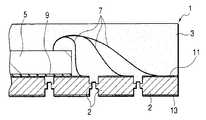
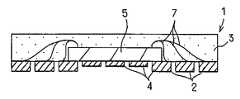
(1) 구리판이나 구리 합금판과 같은 도전성의 평탄 기판(금속판)을 준비하는 공정과, 상기 기판의 주면의 소정 개소에 각각 반도체 소자를 절연성의 접착제로 고정하는 공정과, 상기 반도체 소자의 표면의 각 전극과 상기 반도체 소자로부터 떨어져 있는 상기 기판의 소정의 구획 부분을 도전성 와이어로 전기적으로 접속하는 공정과, 상기 기판의 주면의 대략 전역에 절연성의 수지층을 형성하여 상기 반도체 소자 및 상기 와이어를 덮는 공정과, 상기 기판을 기판의 이면측으로부터 선택적으로 제거하여 적어도 일부가 외부 전극 단자가 되는 전기적으로 독립된 구획 부분(구획 영역)을 복수개 형성하는 공정과, 상기 수지층을 선택적으로 제거하여, 상기 반도체 소자와 상기 반도체 소자의 주위에 위치하는 복수의 구획 부분을 포함하는 영역마다 개편화(fragment)하는 공정에 의해 논-리드형 수지 밀봉형 반도체 장치를 제조한다.(1) a step of preparing a conductive flat substrate (metal plate) such as a copper plate or a copper alloy plate, a step of fixing the semiconductor element at a predetermined position on the main surface of the substrate with an insulating adhesive, and the surface of the semiconductor element Electrically connecting each of the electrodes and a predetermined partition portion of the substrate away from the semiconductor element with a conductive wire, and forming an insulating resin layer over the entire main surface of the substrate to cover the semiconductor element and the wire. Forming a plurality of electrically independent partition portions (compartment regions) in which the substrate is selectively removed from the back surface side of the substrate, and at least a portion thereof becomes an external electrode terminal; and selectively removing the resin layer to form the semiconductor Individualized into regions each including an element and a plurality of partition portions positioned around the semiconductor element A non-lead resin-sealed semiconductor device is manufactured by a process of forming a fragment.
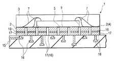
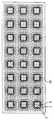
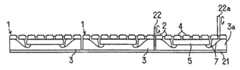
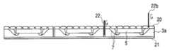
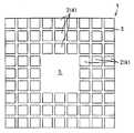
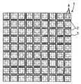
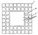
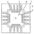
예를 들면, 기판을 바둑판의 눈과 같이 구획 부분(구획 영역)을 상정하고, 복수의 구획 부분에 의한 직사각형 영역을 단위 기판 부분(단위 기판 영역)으로 한다. 이 단위 기판 부분은 기판에 종횡으로 배치되는 것으로 한다. 그리고, 예를 들면 각 단위 기판 부분의 중앙에 반도체 소자를 고정함과 함께, 이 반도체 소자의 전극과 반도체 소자로부터 떨어져 있는 소정의 구획 부분을 와이어로 접속한다. 와이어가 접속되는 구획 부분은 반도체 소자의 외측에 2열 이상 있도록 해둔다. 이어서, 반도체 소자나 와이어를 덮는 수지층을 트랜스퍼 몰드에 의한 편면 몰드에 의해 균일한 두께로 형성한다. 이어서, 수지층의 표면 전역에 지지 부재로서의 테이프를 접착한다. 이어서, 기판을 종횡으로 절단하여 각 구획 부분을 전기적으로 분리시킨다. 분리된 구획 부분의 대부분은 논-리드형 반도체 장치의 실장용 외부 전극 단자로 된다. 이어서, 단위 기판 영역을 서로 독립시키기 위해 수지층을 종횡으로 절단한다. 다음에, 테이프를 박리함으로써 복수의 논-리드형 반도체 장치를 제조한다. 상기 기판 및 수지층의 선택적 제거(분리)는, 예를 들면 다이싱 블레이드에 의한 격자줄무늬 형상의 절단으로 실시한다.For example, suppose a board | substrate part (compartment area) like the eye of a board | substrate, and let rectangular area | region by a some partition part be a unit board | substrate part (unit board | substrate area | region). This unit board | substrate part shall be arrange | positioned longitudinally and horizontally to a board | substrate. For example, while fixing a semiconductor element in the center of each unit board | substrate part, the electrode of this semiconductor element and the predetermined division part separated from a semiconductor element are connected by wire. The partition part to which a wire is connected is made so that two or more rows may be in the outer side of a semiconductor element. Next, the resin layer which covers a semiconductor element and a wire is formed in uniform thickness with the single side mold by a transfer mold. Next, the tape as a support member is stuck to the whole surface of a resin layer. The substrate is then cut longitudinally and horizontally to electrically separate each compartment portion. Most of the separated compartments are external electrode terminals for mounting non-lead semiconductor devices. Next, the resin layer is cut longitudinally and horizontally to separate the unit substrate regions from each other. Next, a plurality of non-lead semiconductor devices are manufactured by peeling the tape. Selective removal (separation) of the said board | substrate and a resin layer is performed by cutting | disconnection of the grid | lattice form shape by a dicing blade, for example.
또한, 반도체 소자를 고정하기 전에, 반도체 소자에 의해 매워지는 반도체 소자 아래에 위치하는 구획 부분과 반도체 소자의 외측에 위치하고 또한 와이어가 접속되는 구획 부분을 도전성 와이어로 접속해둔다. 그리고, 반도체 소자를 고정할 때에, 반도체 소자를 기판에 접착하는 접착제 내에 상기 와이어를 눌러 찌부러뜨림으로써 반도체 소자를 고정한다.In addition, before fixing the semiconductor element, the partition portion located under the semiconductor element filled by the semiconductor element and the partition portion located outside the semiconductor element and to which the wire is connected are connected by conductive wires. And when fixing a semiconductor element, a semiconductor element is fixed by pressing and crushing the said wire in the adhesive agent which adhere | attaches a semiconductor element to a board | substrate.
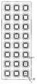
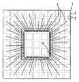
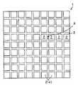
(2) 상기 (1)의 구성에 있어서, 평탄한 도전성 기판의 일면에 에칭에 의해 종횡으로 복수의 홈을 형성하여 바둑판의 눈 형상으로 홈을 둘러싼 구획 부분(구획 영역)을 형성함과 함께, 복수의 구획 부분을 포함하는 직사각형 영역을 논-리드형 반도체 장치를 형성하기 위한 단위 기판 부분(단위 기판 영역)으로 한다. 이 단위 기판 부분은 기판에 종횡으로 정렬 형성(매트릭스 형상 배치)되게 된다.(2) In the configuration of (1), a plurality of grooves are formed on one surface of the flat conductive substrate by etching to form a partition portion (compartment region) surrounding the grooves in the shape of a checkerboard, and a plurality of grooves. The rectangular region including the partition portion of is referred to as a unit substrate portion (unit substrate region) for forming a non-lead semiconductor device. This unit substrate portion is formed to be aligned vertically and horizontally (matrix shape arrangement) on the substrate.
이러한 기판을 사용하는 논-리드형 반도체 장치의 제조 방법은 이하와 같다. 홈이 존재하는 면 또는 홈이 존재하지 않은 면의 각 단위 기판 부분에 반도체 소자를 고정한다. 예를 들면, 단위 기판 부분의 중앙에 반도체 소자를 고정한다. 반도체 소자의 외측에는 복수 열(2열 이상)의 구획 부분이 위치하도록 기판은 형성되어 있다. 이어서, 반도체 소자의 전극과 반도체 소자의 외측에 위치하는 소정의 구획 부분 또는 소정의 구획 부분의 이면을 와이어로 접속한다. 이어서, 반도체 소자 및 와이어를 덮도록 트랜스퍼 몰드에 의한 편면 몰드로 균일한 두께의 수지층을 형성한다. 이어서, 수지층의 표면 전역에 테이프를 접착한다. 그 후, 다이싱 블레이드를 홈의 연재 방향을 따라 상대적으로 이동시키면서 홈 바닥을 절단하고, 기판의 분리, 즉 구획 영역의 분리를 행한다. 이어서, 단위 기판 부분을 서로 독립시키기 위해 수지층을 종횡으로 절단한다. 독립된 단위 기판 부분은 테이프로 지지되어 있다. 이어서, 테이프를 박리함으로써 복수의 논-리드형 반도체 장치를 제조한다.The manufacturing method of the non-lead semiconductor device using such a board | substrate is as follows. The semiconductor element is fixed to each unit substrate portion on the surface where the groove is present or the surface where the groove is not present. For example, the semiconductor element is fixed to the center of the unit substrate portion. The board | substrate is formed in the outer side of a semiconductor element so that the division part of several rows (two or more rows) may be located. Next, the electrode of a semiconductor element and the predetermined partition part located in the outer side of a semiconductor element, or the back surface of the predetermined partition part are connected with a wire. Subsequently, the resin layer of uniform thickness is formed by the single side mold by a transfer mold so that a semiconductor element and a wire may be covered. Next, a tape is stuck to the whole surface of a resin layer. Thereafter, the bottom of the groove is cut while the dicing blade is relatively moved along the extending direction of the groove, and the substrate is separated, that is, the partition region is separated. Next, the resin layer is cut vertically and horizontally to separate the unit substrate portions from each other. Independent unit substrate portions are supported by tape. Next, a plurality of non-lead semiconductor devices are manufactured by peeling the tape.
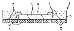
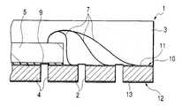
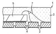
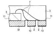
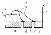
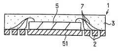
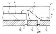
반도체 소자의 주연 부분을 지지하는 구획 부분의 두께에 비교하여 반도체 소자의 중앙에 가까운 영역의 구획 부분을 얇게하거나, 혹은 없애서, 반도체 장치에서 반도체 소자의 하방 부분의 실장면과 실장 기판 사이에 소정의 간극을 발생시 킨다(스탠드 오프 구조).In the semiconductor device, a predetermined portion between the mounting surface and the mounting substrate of the lower portion of the semiconductor element in the semiconductor device is reduced or eliminated by thinning or eliminating the partition portion in the region near the center of the semiconductor element as compared with the thickness of the partition portion supporting the peripheral portion of the semiconductor element. Create a gap (stand-off structure).
또한, 홈이 존재하는 면에 반도체 소자를 고정하는 경우, 구획 부분의 홈 바닥의 제거에 의한 분리를, 기판을 일정 두께 연마나 에칭으로 제거하도록 해도 된다. 또, 홈이 존재하는 면에 반도체 소자를 고정하는 경우, 반도체 소자가 고정되는 영역의 홈을 충전물로 매립한 후, 상기 반도체 소자를 상기 접착제를 이용하여 상기 기판에 고정하고, 상기 반도체 소자와 상기 기판 사이에 공극을 발생시키지 않게 한다. 또한, 상기 기판을 종횡으로 분단하는 교차 개소에 관통 구멍을 형성해둔다.In addition, when fixing a semiconductor element to the surface in which the groove | channel exists, you may make it remove | eliminate the board | substrate by fixed thickness grinding | polishing or etching by removal of the groove bottom of a partition part. In the case where the semiconductor element is fixed to the surface where the groove is present, after filling the groove of the region where the semiconductor element is fixed with a filler, the semiconductor element is fixed to the substrate using the adhesive, and the semiconductor element and the No voids are created between the substrates. In addition, a through hole is formed at an intersection where the substrate is divided longitudinally and horizontally.
(3) 상기 (2)의 구성에 있어서, 평탄한 도전성 기판의 표리면에 에칭에 의해 서로 중첩되도록 대면하는 종횡으로 연재되는 복수의 홈을 형성하여 바둑판의 눈 형상으로 홈을 둘러싼 구획 부분을 형성함과 함께, 복수의 구획 부분을 포함하는 직사각형 영역을 논-리드형 반도체 장치를 형성하기 위한 단위 기판 부분(단위 기판 영역)으로 한다. 이 단위 기판 부분은 기판에 종횡으로 정렬 형성되게 된다. 이러한 기판을 사용하는 논-리드형 반도체 장치의 제조 방법은, 상기 (2)의 경우와 다르고, 항상 홈이 존재하는 면에 반도체 소자를 고정하게 된다.(3) In the configuration of (2), a plurality of vertically extending grooves are formed on the front and rear surfaces of the flat conductive substrate so as to overlap each other by etching to form a partition portion surrounding the grooves in the shape of an eye of a checkerboard. In addition, a rectangular region including a plurality of partition portions is used as a unit substrate portion (unit substrate region) for forming a non-lead semiconductor device. This unit substrate portion is formed to be aligned vertically and horizontally with the substrate. The manufacturing method of the non-lead semiconductor device using such a board | substrate differs from the case of said (2), and always fixes a semiconductor element to the surface in which the groove | channel exists.
(4) 상기 (2) 및 (3)의 구성에 있어서, 기판에서의 단위 기판 부분의 패턴이 다르다. 단위 기판 부분은 반도체 소자를 고정하는 탭과, 이 탭의 각 변으로부터 평행하게 돌출하는 복수의 리드에 의해 구성되고, 리드는 인접하는 다른 단위 기판 부분의 리드에 이어지거나 혹은 기판 프레임에 이어지도록 된다. 단위 기판 부분은 기판에 종횡으로 정렬 배치 형성(매트릭스 형상 배치)되어 있다. 반도체 장치 의 제조에서, 탭은 반도체 소자보다도 큰 형태 혹은 작은 형태(작은 탭)가 취해진다.(4) In the structure of said (2) and (3), the pattern of the unit substrate part in a board | substrate differs. The unit substrate portion is composed of a tab for fixing a semiconductor element and a plurality of leads protruding in parallel from each side of the tab, and the lead is connected to a lead of another adjacent unit substrate portion or to a substrate frame. . The unit board | substrate part is arrange | positioned arrangement | positioning (matrix-shaped arrangement) longitudinally and horizontally in a board | substrate. In the manufacture of a semiconductor device, a tab is taken in a form larger or smaller than a semiconductor element (small tab).
단위 기판 부분이 탭과 리드로 구성되는 구성에서는, 이하의 공정에 의해 논-리드형 반도체 장치를 제조한다.In the structure in which a unit substrate part consists of a tab and a lead, a non-lead semiconductor device is manufactured with the following process.
즉, 도전성 기판을 패터닝하여 반도체 소자를 고정하는 직사각형의 탭과, 이 탭의 소정의 변으로부터 서로 평행하게 연재하여 인접하는 상기 탭으로부터 연재하는 리드 또는 기판 프레임으로 연결되고 또한 리드의 도중에 와이어 접속 영역을 2 개소 이상 갖는 복수의 리드로 이루어지는 단위 기판 부분을 복수개 형성하는 공정과,That is, the wire connection area | region connected to the rectangular tab which patterns a conductive substrate and fixes a semiconductor element, and the lead or board frame which extends in parallel from each other from the said predetermined | prescribed side of this tab, and extends from the adjacent said tab, and is in the middle of a lead. Forming a plurality of unit substrate portions composed of a plurality of leads having two or more positions, and
상기 기판의 주면측의 각 탭 상에 반도체 소자를 접착제를 개재하여 각각 고정하는 공정과,Fixing a semiconductor element on each tab of the main surface side of the substrate via an adhesive agent, respectively;
상기 반도체 소자의 표면의 각 전극과, 상기 리드의 소정의 상기 와이어 접속 영역을 도전성 와이어로 전기적으로 접속하는 공정과,Electrically connecting each electrode on the surface of the semiconductor element and the predetermined wire connection region of the lead with a conductive wire;
상기 기판의 주면측의 대략 전역에 절연성 수지층을 형성하여 상기 반도체 소자 및 상기 와이어를 덮는 공정과,Forming an insulating resin layer on substantially the entire area of the main surface side of the substrate to cover the semiconductor element and the wire;
상기 수지층의 표면 전역에 한장의 테이프를 접착하는 공정과,Bonding a single tape to the entire surface of the resin layer;
상기 리드를 리드 폭 전체 길이에 걸쳐 선택적으로 제거하여 상기 탭, 상기 기판 프레임, 상기 인접하는 단위 기판 영역의 리드 및 인접하는 와이어 접속 영역과 전기적으로 독립시켜 외부 전극 단자를 형성하는 공정과,Selectively removing the lead over the entire length of the lead width to electrically separate the tab, the substrate frame, the lead of the adjacent unit substrate region, and the adjacent wire connection region to form an external electrode terminal;
상기 수지층을 선택적으로 제거하여 상기 단위 기판 부분을 포함하는 단위 기판 영역마다 개편화함과 함께, 테이프를 박리하는 공정에 의해 논-리드형 반도체 장치를 제조한다.A non-lead semiconductor device is produced by a step of selectively removing the resin layer to separate the unit substrate region including the unit substrate portion and peeling the tape.
상기 리드의 선택적 제거 부분은 상기 기판의 종횡을 따르는 각 직선 상에 위치하도록 형성하고 다이싱에 의해 제거한다. 리드의 선택적 제거 시에, 상기 반도체 소자의 표면을 제거하지 않도록 한다. 상기 리드의 선택적 제거는 리드의 길이 방향을 따라서 복수 개소 행해지며, 외부 전극 단자가 반도체 장치의 가장자리를 따라 2열 이상으로 되도록 형성한다. 상기 수지층은 트랜스퍼 몰드에 의한 편면 몰드에 의해 형성하지만, 기판이 몰드 다이의 재치면에 밀착하도록 탭면을 진공 흡인하여 몰드 다이의 재치면에 밀착시키면서 트랜스퍼 몰드를 행한다.The selective removal portion of the lid is formed to be located on each straight line along the longitudinal and transverse sides of the substrate and removed by dicing. In the selective removal of the lead, the surface of the semiconductor element is not removed. Selective removal of the lead is performed in a plurality of places along the length of the lead, and is formed such that the external electrode terminals are arranged in two or more rows along the edge of the semiconductor device. The resin layer is formed by a single-sided mold made by a transfer mold, but the transfer mold is carried out while the tab surface is vacuum sucked so that the substrate is in close contact with the mounting surface of the mold die, and the adhesive surface is in close contact with the mounting surface of the mold die.
상기 (1)의 수단에 따르면, (a) 논-리드형 반도체 장치의 변을 따라 2열 이상 외부 전극 단자를 배치하는 구조로 되기 때문에, 외부 전극 단자를 많게 할 수 있다.According to the said (1) means, since (a) two or more external electrode terminals are arrange | positioned along the side of a non-lead semiconductor device, an external electrode terminal can be increased.
(b) 논-리드형 반도체 장치의 변을 따라 2열 이상 외부 전극 단자를 배치하는 구조로 되기 때문에, 반도체 장치의 소형화를 달성할 수 있다.(b) Since the external electrode terminals are arranged in two or more rows along the sides of the non-lead semiconductor device, miniaturization of the semiconductor device can be achieved.
(c) 외부 전극 단자는 금속판을 다이싱 블레이드에 의해 종횡으로 절단함으로써 형성되기 때문에, 외부 전극 단자의 형상이나 치수 정밀도를 고정밀도로 형성할 수 있다.(c) Since the external electrode terminal is formed by cutting the metal plate vertically and horizontally with the dicing blade, the shape and dimensional accuracy of the external electrode terminal can be formed with high accuracy.
(d) 외부 전극 단자는 금속판을 다이싱 블레이드에 의해 종횡으로 절단함으로써 형성되기 때문에, 외부 전극 단자의 주연부에는 절단에 의한 긴 돌기(가공 돌기)는 발생하여 어렵게 되어 전극 평탄도가 향상된다. 이 결과, 땜납 등을 이용하 여 실장 기판에 논-리드형 반도체 장치를 실장한 경우, 상기 돌기에 의한 외부 전극 단자의 실장 기판의 랜드(배선)와의 접속 불량이 일어나기 어려워서, 실장 강도의 향상이나 실장의 신뢰성이 향상된다.(d) Since the external electrode terminal is formed by cutting the metal plate vertically and horizontally by the dicing blade, long protrusions (machining protrusions) due to cutting occur on the periphery of the external electrode terminal, making it difficult, thereby improving electrode flatness. As a result, in the case where the non-lead semiconductor device is mounted on the mounting substrate using solder or the like, poor connection with lands (wiring) of the mounting board of the external electrode terminal due to the projections is unlikely to occur, thereby improving the mounting strength or mounting. The reliability of the is improved.
(e) 반도체 소자에 의해 매워지는 영역의 구획 부분과, 반도체 소자 외측의 와이어가 접속되는 구획 부분을 와이어로 접속한 구조에서는, 반도체 소자 아래의 영역에도 외부 전극 단자를 배치할 수 있게 되어, 실장 기판에서의 배선 패턴 형성의 여유도가 향상될뿐만 아니라, 배선 패턴의 변경에 의해 실장 기판의 소형화도 달성할 수 있다.(e) In the structure in which the partition portion of the region filled by the semiconductor element and the partition portion to which the wire outside the semiconductor element is connected by a wire, the external electrode terminal can be arranged in the region under the semiconductor element, and thus the mounting Not only can the margin of wiring pattern formation on the substrate be improved, but the miniaturization of the mounting substrate can be achieved by changing the wiring pattern.
(f) 한장의 금속판의 절단으로 용이하게 구획 부분(외부 전극 단자)을 형성할 수 있어, 반도체 장치의 제조 비용의 저감을 달성할 수 있다.(f) A partition part (external electrode terminal) can be formed easily by cutting | disconnecting a piece of metal plate, and the reduction of the manufacturing cost of a semiconductor device can be achieved.
상기 (2)의 수단에 따르면, (a) 논-리드형 반도체 장치의 변을 따라 2열 이상 외부 전극 단자를 배치하는 구조로 되기 때문에, 외부 전극 단자를 많게 할 수 있다.According to said means (2), since (a) two or more external electrode terminals are arrange | positioned along the side of a non-lead semiconductor device, an external electrode terminal can be increased.
(b) 논-리드형 반도체 장치의 변을 따라 2열 이상 외부 전극 단자를 배치하는 구조로 되기 때문에, 반도체 장치의 소형화를 달성할 수 있다.(b) Since the external electrode terminals are arranged in two or more rows along the sides of the non-lead semiconductor device, miniaturization of the semiconductor device can be achieved.
(c) 외부 전극 단자는 금속판을 다이싱 블레이드에 의해 종횡으로 절단함으로써 형성되기 때문에, 외부 전극 단자의 형상이나 치수 정밀도를 고정밀도로 형성할 수 있다.(c) Since the external electrode terminal is formed by cutting the metal plate vertically and horizontally with the dicing blade, the shape and dimensional accuracy of the external electrode terminal can be formed with high accuracy.
(d) 외부 전극 단자는 금속판을 다이싱 블레이드에 의해 종횡으로 절단함으로써 형성되기 때문에, 외부 전극 단자의 주연부에는 절단에 의한 긴 돌기(가공 돌 기)는 발생하기 어렵게 되어 전극 평탄도가 향상된다. 이 결과, 땜납 등을 이용하여 실장 기판에 논-리드형 반도체 장치를 실장한 경우, 상기 돌기에 의한 외부 전극 단자의 실장 기판의 랜드(배선)와의 접속 불량이 일어나기 어려워, 실장 강도의 향상이나 실장의 신뢰성이 향상된다.(d) Since the external electrode terminal is formed by cutting the metal plate vertically and horizontally by the dicing blade, long projections (machining projections) due to cutting are less likely to occur at the periphery of the external electrode terminals, thereby improving electrode flatness. As a result, in the case where the non-lead semiconductor device is mounted on the mounting substrate using solder or the like, poor connection with lands (wiring) of the mounting board of the external electrode terminal due to the projections is unlikely to occur, thereby improving the mounting strength or mounting. The reliability of the is improved.
(e) 한장의 금속판을 종횡으로 다이싱 블레이드로 다이싱하는 것만으로 복수의 반도체 장치의 외부 전극 단자를 형성할 수 있기 때문에, 반도체 장치의 제조 비용의 저감을 달성할 수 있다.(e) Since the external electrode terminals of the plurality of semiconductor devices can be formed only by dicing one sheet of metal plate with the dicing blade in the vertical and horizontal directions, the manufacturing cost of the semiconductor device can be reduced.
(f) 기판에 홈을 형성하고, 수지층 형성 후에 홈 바닥을 제거함으로써 전기적으로 분리된 구획 영역을 형성할 수 있어, 구획 부분의 분리 시간이 보다 단축되어 반도체 장치의 제조 시간의 단축을 도모할 수 있다. 또한, 절단 시간의 단축에 의해, 다이싱 블레이드의 마모도 적어져서 블레이드의 수명도 길어진다. 이들에 의해, 반도체 장치의 제조 비용의 저감을 달성할 수 있다.(f) By forming a groove in the substrate and removing the groove bottom after the resin layer is formed, an electrically separated partition region can be formed, so that the separation time of the partition portion can be shortened and the manufacturing time of the semiconductor device can be shortened. Can be. In addition, by shortening the cutting time, the wear of the dicing blade is reduced, and the life of the blade is also long. By these, reduction of the manufacturing cost of a semiconductor device can be achieved.
(g) 홈은 에칭으로 형성할 수 있기 때문에, 홈의 가장자리에 가공 돌기가 발생하지 않는다. 따라서, 홈이 존재하지 않는 면에 반도체 소자를 고정하는 제조 방법의 경우에는, 구획 부분에 의해 형성되는 외부 전극 단자의 전극 평탄도가 양호하게 되어, 반도체 장치의 실장의 신뢰성이 높아진다.(g) Since the grooves can be formed by etching, no processing projections occur at the edges of the grooves. Therefore, in the case of the manufacturing method of fixing a semiconductor element to the surface where a groove does not exist, the electrode flatness of the external electrode terminal formed by the partition part becomes favorable, and the reliability of the mounting of a semiconductor device becomes high.
(h) 스탠드 오프 구조로 함으로써, 실장 시에, 가령 실장 기판 상에 이물질이 존재하고 있어도 지장을 주지는 않는다.(h) By setting it as a standoff structure, even if a foreign material exists on a mounting board | substrate at the time of mounting, it does not interfere.
(i) 홈이 존재하는 면에 반도체 소자를 고정하는 경우, 구획 부분의 홈 바닥의 제거에 의한 분리를, 기판을 일정 두께 연마나 에칭으로 제거하도록 해도 된다. 이 경우, 외부 전극 단자의 전극 평탄도를 양호하게 할 수 있다.(i) In the case where the semiconductor element is fixed to the surface where the groove is present, the substrate may be removed by a constant thickness grinding or etching by removal of the groove bottom of the partition portion. In this case, the electrode flatness of the external electrode terminal can be improved.
(j) 기판을 종횡으로 분단하는 교차 개소에 관통 구멍을 형성해 둠으로써, 다이싱 블레이드에 의한 절단 시간을 짧게 할 수 있음과 함께, 블레이드의 장기 수명화를 도모할 수 있다.(j) By forming a through hole in the intersection where the substrate is divided longitudinally and horizontally, the cutting time by the dicing blade can be shortened and the life of the blade can be extended.
(k) 홈이 존재하는 면에 반도체 소자를 고정하는 경우, 반도체 소자가 고정되는 영역의 홈을 충전물로 매립함으로써 반도체 소자와 기판 사이에 공극이 발생하지 않게 되어, 반도체 소자와 기판과의 고정면에 수분이 저장되지 않기 때문에, 반도체 장치의 땜납 리플로우에 의한 실장 시에, 상기 수분의 팽창에 기인하는 실장 불량이 발생하기 어려워진다.(k) In the case where the semiconductor element is fixed to the surface where the groove is present, the gap between the semiconductor element and the substrate is not generated by filling the groove of the region where the semiconductor element is fixed with the filling material, and the fixing surface of the semiconductor element and the substrate is prevented. Since moisture is not stored in the package, mounting failure due to expansion of the moisture is less likely to occur at the time of mounting by solder reflow of the semiconductor device.
상기 (3)의 수단에 따르면, 상기 (2)의 구성에 의한 효과를 가짐과 함께, (a) 기판의 표리면에 대면하여 홈을 형성하고, 기판의 구획 영역의 분리 시에는 다이싱 블레이드를 홈의 연재 방향을 따라 상대적으로 이동시키면서 표리의 홈의 홈 바닥을 절단하는 것뿐이기 때문에, 구획 부분의 분리 시간이 보다 단축되어 반도체 장치의 제조 시간의 단축을 도모할 수 있다. 또한, 절단 시간의 단축에 의해, 다이싱 블레이드의 마모도 적어져서 블레이드의 수명도 길어진다. 이에 따라, 반도체 장치의 제조 비용의 저감을 달성할 수 있다.According to the said (3) means, while having the effect by the structure of said (2), (a) groove | channel is formed facing the front and back of a board | substrate, and a dicing blade is carried out at the time of the division | dividing of the partition area of a board | substrate. Since only the groove bottom of the grooves in the front and back is cut while being relatively moved along the extending direction of the grooves, the separation time of the partition portion can be shortened and the manufacturing time of the semiconductor device can be shortened. In addition, by shortening the cutting time, the wear of the dicing blade is reduced, and the life of the blade is also long. Thereby, the manufacturing cost of a semiconductor device can be reduced.
상기 (4)의 수단에 따르면, (a) 논-리드형 반도체 장치의 변을 따라 2열 이상 외부 전극 단자를 배치하는 구조가 되기 때문에, 외부 전극 단자를 많게 할 수 있다.According to said means (4), since (a) the structure which arrange | positions two or more external electrode terminals along the side of a non-lead semiconductor device, an external electrode terminal can be made large.
(b) 논-리드형 반도체 장치의 변을 따라 2열 이상 외부 전극 단자를 배치하 는 구조가 되기 때문에, 반도체 장치의 소형화를 달성할 수 있다.(b) Since the external electrode terminals are arranged in two or more rows along the sides of the non-lead semiconductor device, the semiconductor device can be miniaturized.
(c) 외부 전극 단자는 금속판(리드)을 다이싱 블레이드에 의해 여러개소로 절단함으로써 형성되기 때문에, 외부 전극 단자의 형상이나 치수 정밀도를 고정밀도로 형성할 수 있다.(c) Since the external electrode terminal is formed by cutting the metal plate (lead) into several places by the dicing blade, the shape and dimensional accuracy of the external electrode terminal can be formed with high accuracy.
(d) 외부 전극 단자는 금속판(리드)을 다이싱 블레이드에 의해 여러개소로 절단함으로써 형성되기 때문에, 외부 전극 단자의 주연부에는 절단에 의한 긴 돌기(가공 돌기)는 발생하기 어려워 전극 평탄도가 향상된다. 이 결과, 땜납 등을 이용하여 실장 기판에 논-리드형 반도체 장치를 실장한 경우, 상기 돌기에 의한 외부 전극 단자의 실장 기판의 랜드(배선)와의 접속 불량이 일어나기 어려워, 실장 강도의 향상이나 실장의 신뢰성이 향상된다.(d) Since the external electrode terminal is formed by cutting the metal plate (lead) into several places by the dicing blade, long protrusions (machining protrusions) due to cutting are hardly generated at the periphery of the external electrode terminal, thereby improving electrode flatness. do. As a result, in the case where the non-lead semiconductor device is mounted on the mounting substrate using solder or the like, poor connection with lands (wiring) of the mounting board of the external electrode terminal due to the projections is unlikely to occur, thereby improving the mounting strength or mounting. The reliability of the is improved.
(e) 한장의 금속판을 종횡으로 다이싱 블레이드로 다이싱하는 것만으로 복수의 반도체 장치의 외부 전극 단자를 형성할 수 있기 때문에, 반도체 장치의 제조 비용의 저감을 달성할 수 있다.(e) Since the external electrode terminals of the plurality of semiconductor devices can be formed only by dicing one sheet of metal plate with the dicing blade in the vertical and horizontal directions, the manufacturing cost of the semiconductor device can be reduced.
(f) 외부 전극 단자는 다이싱 블레이드로 리드를 그 폭 방향으로 절단함으로써 형성할 수 있으므로, 절단 시간의 단축을 도모할 수 있음과 함께, 절단 시간이 짧기 때문에 다이싱 블레이드의 마모도 적어져서 블레이드의 수명도 길어진다. 이에 따라, 반도체 장치의 제조 비용의 저감을 달성할 수 있다.(f) Since the external electrode terminal can be formed by cutting the lead with the dicing blade in the width direction thereof, the cutting time can be shortened, and the cutting time is short, so that the wear of the dicing blade is reduced so that the blade It also extends its lifespan. Thereby, the manufacturing cost of a semiconductor device can be reduced.
(g) 트랜스퍼 몰드에 의한 수지층의 형성 시에, 기판이 몰드 다이의 재치면에 진공 흡인에 의해 밀착하기 때문에, 리드면도 상기 재치면에 밀착하므로, 탭의 이면 및 리드의 이면에 수지가 돌아서 유입되지 않게 된다. 이 결과, 외부 전극 단자의 실장면의 수지에 의한 오염을 방지할 수 있어, 실장의 신뢰성이 높은 논-리드형 반도체 장치를 제조할 수 있다.(g) Since the substrate is in close contact with the mounting surface of the mold die by vacuum suction at the time of formation of the resin layer by the transfer mold, the lead surface is also in close contact with the mounting surface, so that the resin is turned on the back surface of the tab and the back surface of the lid. It does not flow in. As a result, contamination by resin of the mounting surface of an external electrode terminal can be prevented, and the non-lead semiconductor device with high mounting reliability can be manufactured.
본원에 있어서 개시되는 발명 중 대표적인 것에 의해 얻어지는 효과를 간단히 설명하면 하기와 같다. 본 발명은 여기에 기재하는 모든 효과를 달성하는 구성에 한정하는 것은 아니고, 여기에 기재하는 효과의 일부를 달성하는 구성도 본 발명의 구성으로서 포함하는 것이다.When the effect obtained by the typical thing of the invention disclosed in this application is demonstrated briefly, it is as follows. This invention is not limited to the structure which achieves all the effects described here, and also includes the structure which achieves some of the effects described here as a structure of this invention.
(1) 소형의 논-리드형 반도체 장치를 제공할 수 있다.(1) A small non-lead semiconductor device can be provided.
(2) 외부 전극 단자수를 많게 할 수 있는 논-리드형 반도체 장치를 제공할 수 있다.(2) A non-lead semiconductor device capable of increasing the number of external electrode terminals can be provided.
(3) 반도체 장치의 변을 따라 2열 이상 외부 전극 단자를 배치할 수 있는 논-리드형 반도체 장치의 제조 방법을 제공할 수 있다.(3) The manufacturing method of the non-lead semiconductor device which can arrange | position two or more external electrode terminals along the side of a semiconductor device can be provided.
(4) 외부 전극 단자의 형상이나 치수 정밀도를 고정밀도로 형성할 수 있는 논-리드형 반도체 장치의 제조 방법을 제공할 수 있다.(4) The manufacturing method of the non-lead semiconductor device which can form the shape and dimensional precision of an external electrode terminal with high precision can be provided.
(5) 실장의 신뢰성이 높은 논-리드형 반도체 장치를 제공할 수 있다.(5) A non-lead semiconductor device having high mounting reliability can be provided.
이하, 도면을 참조하여 본 발명의 실시 형태를 상세히 설명한다. 또, 발명의 실시 형태를 설명하기 위한 모든 도면에 있어서, 동일 기능을 갖는 것은 동일 부호를 붙여서 그 반복된 설명은 생략한다.EMBODIMENT OF THE INVENTION Hereinafter, embodiment of this invention is described in detail with reference to drawings. In addition, in all the figures for demonstrating embodiment of this invention, the thing with the same function attaches | subjects the same code | symbol, and the repeated description is abbreviate | omitted.
(실시 형태 1)(Embodiment 1)
도 1 내지 도 13은 본 발명의 일 실시 형태(실시 형태 1)의 논-리드형 수지 밀봉형의 반도체 장치의 제조 방법에 관한 도면이다. 본 실시 형태 1에서는, 도 1 내지 도 4에 도시한 바와 같이, 사각형의 수지 밀봉체(33)의 이면에 도전체(금속)로 이루어지는 외부 전극 단자(2)가 노출되는 논-리드형 반도체 장치(1)의 제조 방법에 본 발명을 적용한 예에 대하여 설명한다.1 to 13 are diagrams illustrating a method for manufacturing a non-lead resin-sealed semiconductor device of one embodiment (Embodiment 1) of the present invention. In the first embodiment, as shown in FIGS. 1 to 4, a non-lead semiconductor device in which an
본 실시 형태 1에서는, 도 1 및 도 2에 도시한 바와 같이, 소정의 두께의 직사각형으로 이루어지는 수지 밀봉체(3)의 이면(실장면측)에 바둑판의 눈 형상으로 전기적으로 독립된 구획 부분(구획 영역: 4)을 갖는 구조로 되어 있다. 본 실시 형태 1에서는, 사각형이 되는 수지 밀봉체(3)의 각 변을 따라 배열하는 2열의 구획 부분(4)을 외부 전극 단자(2)로서 사용하는 반도체 장치에 대하여 설명한다.In this
구획 부분(구획 영역: 4)은, 예를 들면 종횡이 각각 0.5㎜가 되는 사각형이다. 또한, 구획 영역(4)과 구획 영역(4) 사이의 간극은, 예를 들면 약 0.15㎜이다. 외부 전극 단자 피치를 0.5㎜로 한 경우에는 구획 영역(4)은 종횡의 치수가 각각 0.35㎜가 된다. 수지 밀봉체(3) 내에는 반도체 소자(반도체 칩: 5)가 위치함과 함께, 이 반도체 소자(5)의 전극(6)(도 3 참조)과, 소정의 구획 부분(4)의 수지 밀봉체(3)로 덮어지는 면측은 도전성 와이어(7)로 전기적으로 접속되어 있다. 와이어(7)도 수지 밀봉체(3)로 덮어져 있다.The partition portion (compartment region: 4) is, for example, a rectangle having a vertical and horizontal width of 0.5 mm. In addition, the clearance between the
반도체 소자(5)는 복수의 구획 부분(4)에 접착제(9)로 고정되어 있다. 접착제(9)는 도전성이나 절연성을 갖는 것이어도 된다. 본 예에서는 도전성의 접착제, 예를 들면 은(Ag) 페이스트가 사용되고 있다. 따라서, 예를 들면 반도체 칩의 구 획 부분(4)에 접촉하는 기판 부분이 전기적으로 사용되지 않은 층인 경우에는, 반도체 소자(5)에 도전성의 접착제(9)를 개재하여 접속되는 각 구획 부분(4)은 외부 전극 단자로서는 사용되지 않는다. 그러나, 이 경우도 실장용 단자로서는 사용 가능하다. 또한, 이 경우, 후술하는 다른 각 실시 형태와 같이, 반도체 소자(5)의 외측에 위치하는 와이어(7)가 접속된 구획 부분(4)과, 반도체 소자(5)에 덮어지는 아래에 위치하는 일부의 구획 부분(4)을 와이어나 구획 부분(4)을 형성하는 재질 부분에서 접속 상태로 함으로써, 반도체 소자(5) 아래에 위치하는 구획 부분(4)도 외부 전극 단자(2)로서 사용할 수 있다.The
또한, 반도체 칩의 구획 부분(4)에 접촉하는 기판 부분이 접지 전위로서 사용되는 경우에는, 반도체 소자(5)에 접착제(9)를 개재하여 접속된 구획 부분(4)은 외부 전극 단자(2)로서의 접지 전극으로서 사용할 수 있다.In addition, when the board | substrate part which contacts the
접착제(9)로서 절연성인 것을 사용하면, 반도체 소자(5)에 접착제(9)를 개재하여 접속되는 각 구획 부분(4)은 각각 전기적으로 독립된 것으로 된다. 또, 외부 전극 단자(2)로서 사용되지 않은 구획 부분(4)도 반도체 장치(1)의 실장 시 땜납 등의 접합재를 이용하여 배선 기판 등에 고정하는 구조로 함으로써, 실장 강도를 높일 수 있다. 또한, 방열성의 향상도 가능해진다. 이 구조에 있어서도, 상술한 바와 같이 반도체 소자(5)의 외측에 위치하는 와이어(7)가 접속된 구획 부분(4)과, 반도체 소자(5)에 덮어지는 아래에 위치하는 일부 구획 부분(4)을 와이어나 구획 부분(4)을 형성하는 재질 부분에서 접속 상태로 함으로써, 반도체 소자(5) 아래에 위치하는 구획 부분(4)도 외부 전극 단자(2)로서 사용할 수 있다.If an insulating thing is used as the
구획 부분(4)의 와이어(7)가 접속되는 면(내면: 10)에는 도 5에 도시한 바와 같이 도금막(11)이 형성되어 있다. 이 도금막(11)은, 와이어(7)와의 접착성을 양호하게 하기 위해서 형성되는 것이다. 예를 들면, 와이어(7)는, 예를 들면 Au선이 사용되고, 도금막(11)은, 예를 들면 Ag 도금막, Au 도금막 또는 Pd 도금막으로 된다.As shown in FIG. 5, the
또한, 구획 부분(4)의 이면(실장면: 12)에는 실장 시에 사용하는 외장 도금막(13)이 형성되어 있다. 이 외장 도금막(13)은 반도체 장치(1)를 모듈 기판 등의 배선 기판에 실장할 때 사용하는 접합재와의 접합성(누설 특성)을 양호하게 하기 위해서 형성되는 것이다. 접합재로서 PbSn 땜납을 사용하는 경우에는, 외장 도금막(13)은 PbSn 땜납 도금막이 바람직하고, 본 실시 형태 1에서는 PbSn 땜납 도금막이 사용되고 있다.Moreover, the
본 실시 형태 1에서는, 반도체 소자(5)의 외측에 위치하는 구획 부분(4)은 직사각형의 수지 밀봉체(3)의 각 변을 따라 2열로 되어 있다. 또한, 이 2열의 구획 부분(4), 즉 외부 전극 단자(2)에서는 도 2 및 도 3에 도시한 바와 같이 와이어(7)가 접속되지 않은 외부 전극 단자도 존재하고 있다.In the first embodiment, the
도 6은 본 실시 형태 1의 반도체 장치(1)를 전자 기기에 내장한 상태, 즉 전자 기기의 마더 보드나 모듈 기판 등의 배선 기판(15)에 실장한 상태를 나타내는 단면도이다. 다층 배선 구조로 이루어지는 배선 기판(15)의 주면에는, 배선(16)의 일부에 의해 반도체 장치(1)의 각 외부 전극 단자(2)에 대응하는 랜드(17)가 형성되어 있다. 그리고, 이들 랜드(17)에 땜납(PbSn 땜납: 18)을 통해 반도체 장치(1) 의 외부 전극 단자(2)가 전기적으로 접속되어 있다.FIG. 6 is a cross-sectional view showing a state in which the
이어서, 이러한 반도체 장치의 제조 방법에 대하여 설명한다. 즉, 반도체 장치는 금속판으로 이루어지는 기판의 일면에 소정의 간격을 두고 반도체 소자를 고정한 후, 반도체 소자의 각 전극과 반도체 소자 외측의 소정의 기판 영역을 도전성 와이어로 접속하고, 이어서 기판의 일면을 트랜스퍼 몰드에 의한 편면 몰드에 의해 일정 두께의 수지층을 형성하여 반도체 소자나 와이어를 덮은 후, 기판을 격자줄무늬 형상으로 종횡으로 절단하여 바둑판의 눈 형상으로 구획 부분(구획 영역)을 형성하고, 또한 수지층을 종횡으로 절단하여 개편화함으로써 제조된다. 그리고, 와이어 접속 부분은 어느 하나의 구획 부분에 접속되도록 한다. 또한, 개편화는 하나의 반도체 소자와, 이 반도체 소자의 주위에 위치하는 복수의 구획 부분을 포함하는 직사각형 영역마다의 분단으로 된다. 또한, 상기 수지층을 절단함으로써 반도체 장치의 수지 밀봉체가 형성되게 된다.Next, the manufacturing method of such a semiconductor device is demonstrated. That is, in the semiconductor device, the semiconductor device is fixed to one surface of a substrate made of a metal plate at a predetermined interval, and then, each electrode of the semiconductor device and a predetermined substrate region outside the semiconductor device are connected with conductive wires, and then one surface of the substrate is transferred. After forming a resin layer having a predetermined thickness by covering a semiconductor element or a wire by a single-sided mold by a mold, the substrate is cut longitudinally and horizontally into a lattice pattern to form a partition portion (compartment region) in the shape of an eye of a checker board. It is produced by cutting the strata vertically and laterally into individual pieces. The wire connecting portion is connected to any one of the partition portions. In addition, individualization becomes division | segmentation for every rectangular area | region containing one semiconductor element and the some partition part located around this semiconductor element. Moreover, the resin sealing body of a semiconductor device is formed by cut | disconnecting the said resin layer.
이어서, 도 7의 공정 단면도를 참조하면서 반도체 장치의 제조에 대하여 보다 구체적으로 설명한다. 본 공정 단면도에서는, 도면의 명료함을 위하여 해칭을 넣지 않은 도면을 이용하여 설명한다. 또, 이하의 각 실시 형태에서도 마찬가지로 해칭을 넣지 않은 도면을 이용하여 설명하는 경우도 있다.Next, the manufacturing of the semiconductor device will be described in more detail with reference to the cross-sectional view of FIG. 7. In this process sectional drawing, it demonstrates using drawing which is not hatched for clarity of drawing. Moreover, also in each of the following embodiments, it may be demonstrated using drawing which has not attached hatching similarly.
논-리드형 반도체 장치의 제조에서는, 최초로 도 7의 (a)에 도시한 바와 같이, 한장의 도전성 기판(20)을 준비한다. 이 기판(20)은 반도체 장치의 제조에서 통상 사용되는 구리 합금판, 구리판, 철-니켈 합금판 등의 금속판으로 이루어져 있다. 본 실시 형태 1에서는 평탄한 구리판을 사용한다. 또한, 이 기판(20)은, 도 8에 도시한 바와 같이, 한번에 복수의 반도체 장치를 제조할 수 있는 크기의 직사각형의 평판(장방형 판)이 되고, 예를 들면 3행 8열로 24개의 반도체 장치를 제조할 수 있는 것으로 되어 있다. 또한, 기판(20)의 일면, 즉 반도체 소자를 고정하는 주면에는 반도체 소자의 접합성이나 와이어의 접속성을 향상시키기 위해서, 도 7에서는 도시하지 않았지만 Ag으로 이루어지는 도금막(11)(도 5 참조)이 형성되어 있다. 기판(20)의 두께는, 예를 들면 0.125 ∼ 0.2㎜의 두께로 되어 있다.In the manufacture of the non-lead semiconductor device, as shown in FIG. 7A, a single
이어서, 도 7의 (b) 및 도 8에 도시한 바와 같이, 도시하지 않은 상용의 칩 본딩 장치를 이용하여 기판(20)의 주면에 반도체 소자(5)를 고정한다. 반도체 소자(5)는, 도 5에 도시한 바와 같이, Ag 페이스트로 이루어지는 접착제(9)로 고정한다. 이 때, 후속 공정의 다이싱 블레이드에 의한 기판(20)의 절단 시에, 반도체 소자(5)의 이면(고정면)을 절단하지 않도록 하기 위해서, 접착제(9)의 두께를, 예를 들면 30 ∼ 100㎛ 정도로 두껍게 하고, 다이싱 블레이드의 선단이 접착제(9)의 중간층에서 그치도록 한다. 이 칩 본딩에 있어서, 반도체 소자(5)는 기판(20)의 주면에 종횡으로 소정의 간격을 두고 정렬 배치(매트릭스 형상으로 배치) 고정된다. 각 반도체 소자(5) 사이에는 소정 간격의 영역이 넓어지고, 이 영역이 각 반도체 장치의 외주연으로 된다. 따라서, 기판(20)은 어떤 패터닝도 되어 있지 않지만, 상기 각 반도체 소자의 외주연으로 둘러싸인 직사각형의 영역 부분이 논-리드형 반도체 장치를 하나 형성하기 위한 단위 기판 부분(단위 기판 영역)으로 된다.Subsequently, as shown in FIGS. 7B and 8, the
이어서, 도 7의 (c) 및 도 8에 도시한 바와 같이, 반도체 소자(5) 표면의 전극(6)(도 3 참조)과, 반도체 소자(5) 주위로 넓어지는 직사각형 프레임 영역의 소 정의 구획 부분으로 되는 영역(4)을 도전성 와이어(7)로 접속한다. 와이어(7)는, 예를 들면 금선을 이용하고, 도시하지 않은 와이어 본딩 장치를 이용하여 행한다.Subsequently, as illustrated in FIGS. 7C and 8, the definition of the electrode 6 (see FIG. 3) on the surface of the
이어서, 도 7의 (d)에 도시한 바와 같이, 반도체 소자(5) 및 와이어(7)를 덮도록, 예를 들면 도시하지 않은 트랜스퍼 몰드 장치를 이용하여, 기판(20)의 주면 상에 절연성 수지에 의한 수지층(3a)을 형성한다. 수지층(3a)은 균일한 두께로 형성되고, 반도체 소자(5)나 와이어(7)는 간극없이 수지로 덮어지게 된다. 이 수지층(3a)의 두께는 반도체 소자(5)나 와이어(7)를 덮고, 반도체 장치의 내습성을 저하시키지 않는 것을 조건으로 하여, 반도체 장치의 박형화를 위해 얇을수록 좋다. 수지층(3a)을 형성하는 절연성 수지로서는, 예를 들면 에폭시 수지가 사용된다. 수지층(3a)은 트랜스퍼 몰드 이외의 수지 충전 방법으로 형성해도 된다. 즉, 다중 노즐을 갖는 디스펜서에 의한 도포 등으로 형성해도 된다.Subsequently, as illustrated in FIG. 7D, the insulating surface is insulated on the main surface of the
이어서, 도 7의 (e)에 도시한 바와 같이, 기판(20)의 이면에 외장 도금막(13)을 형성한다. 도 7의 (e)에서는 부호만 나타낸다. 외장 도금막(13)에 대해서는 도 5에 도시하고 있다. 또한, 예를 들면 외장 도금막(13)은 PbSn 땜납으로 형성되고, 예를 들면 전계 도금법에 의해 형성된다. 외장 도금막(13)의 두께는 5 ∼ 20㎛ 정도로 형성된다.Subsequently, as shown in FIG. 7E, the
이어서, 도 7의 (f)에 도시한 바와 같이, 수지층(3a)의 표면 전역에 지지 부재로서의 테이프(21)를 접착한다. 그 후, 기판(20)을 상면이 되도록 하여 다이싱 블레이드(22)로 기판(20)을 종횡으로 절단하고, 사각형(직사각형)으로 이루어지는 구획 부분(4)을 형성한다. 다이싱 블레이드(22)에 의한 절단 부분은, 도 4에 도시 한 바와 같이, 격자줄무늬로 되고, 그 사이에는 바둑판의 눈 형상으로 구획 부분(4)이 형성되게 된다. 다이싱 블레이드(22)는, 예를 들면 두께 150㎛의 것을 이용하는 결과, 1변이 0.5㎜인 구획 부분(4)이 바둑판의 눈 형상으로 0.65㎜ 피치로 형성된다. 이 다이싱에 있어서는 기판(20)을 확실하게 절단하기 위해서 다이싱 블레이드의 선단은 기판(20)을 통과하는 깊이까지 다이싱되지만, 반도체 소자(5)의 이면을 절삭하지 않게 한다. 이 때문에, 다이싱 홈 바닥은 반도체 소자(5)를 기판(20)에 고정하는 접착제(9)의 도중 깊이에 위치하도록 한다. 수지층(3a) 내측의 표층 부분에 다이싱 홈이 형성되어도 특별히 지장은 없다.Subsequently, as shown in FIG. 7F, the
또한, 단위 기판 영역과 단위 기판 영역의 경계는, 상기 다이싱 블레이드(22)로 절단되지만, 수지층(3a)도 동시에 절단된다. 수지층(3a)의 절단에 의해 개편화가 도모되고, 테이프(21)에 접착한 상태이어도 반도체 장치(1)가 복수개 제조된다. 반도체 소자(5)나 와이어(7)를 덮는 수지층(3a)은 이 절단에 의해 수지 밀봉체(3)로 된다.In addition, although the boundary of a unit board | substrate area | region and a unit board | substrate area | region is cut | disconnected with the said
또한, 수지층(3a)은 절단할 경우에는 테이프(21)를 완전하게 절단하지 않도록 한다. 이것은 절단이 XY 방향의 2 방향으로 행해지기 때문에, 한 방향의 절단 후에도 각부는 테이프(21)에 유지되어 있는 것이 바람직하다.In the case of cutting the
또한, 다이싱 블레이드(22)는 한장의 블레이드라도 되며, 또한 복수매의 블레이드를 갖고, 동시에 평행하게 복수개의 절단을 행하는 다이싱 블레이드라도 상관없다.The
또한, 상기 실시 형태에서는 구획 부분(4)의 형성 시 및 개편화 시에, 수지 층(3a) 표면 전역에 지지 부재로서 테이프(21)를 접착하여 다이싱 블레이드로 절단하는 예를 설명하였지만, 반드시 이에 한정되지는 않고, 테이프(21)를 대신하여 고정용 지그로 수지층(3a)을 지지할 수도 있다.Moreover, although the said embodiment demonstrated the example which adhere | attaches the
이어서, 도 7의 (g)에 도시한 바와 같이, 테이프(21)를 수지 밀봉체(3)로부터 박리 제거시킴으로써 논-리드형 반도체 장치(1)가 다수개 제조된다. 본 실시 형태 1의 반도체 장치(1)는, 외부 전극 단자(2)가 반도체 장치(1)의 가장자리(변)를 따라 각각 2열이 되는 구조로 되어 있다.Subsequently, as shown in FIG. 7G, a plurality of
본 실시 형태 1에 따르면 이하의 효과를 갖는다.According to the first embodiment, the following effects are obtained.
(1) 논-리드형 반도체 장치의 주연부(변)를 따라 외부 전극 단자(2)를 2열로 배치하는 구조로 되기 때문에, 외부 전극 단자(2)를 많게 할 수 있다.(1) Since the
(2) 외부 전극 단자를 많이 필요로 하는 논-리드형 반도체 장치에서는, 수지 밀봉체의 1변을 따라 1열로 외부 전극 단자를 배열하기 때문에, 수지 밀봉체의 1변의 길이를 길게 해야만 하고, 수지 밀봉체가 커져서 반도체 장치가 대형화되지만, 본 실시 형태 1의 경우에는, 반도체 장치의 각 변을 따라 2열로 외부 전극 단자(2)를 배치하는 구성으로 되기 때문에, 수지 밀봉체(33)를 작게 할 수 있어 반도체 장치(1)의 소형화를 달성할 수 있다.(2) In the non-lead semiconductor device which requires a lot of external electrode terminals, since the external electrode terminals are arranged in one row along one side of the resin encapsulation member, the length of one side of the resin encapsulation member must be lengthened, and the resin Although the sealing body becomes large and a semiconductor device becomes large, in this
(3) 상기 (1) 및 (2)에 의해, 작은 수지 밀봉체라도 외부 전극 단자(2)의 수를 많게 할 수 있어, 다단자화를 달성할 수 있다. 이것은 다기능 반도체 장치로서는 바람직하다.(3) By said (1) and (2), even if it is a small resin sealing body, the number of
(4) 외부 전극 단자(2)는 금속판을 다이싱 블레이드에 의해 종횡으로 절단함 으로써 형성되기 때문에, 외부 전극 단자(2)의 형상이나 치수 정밀도를 고정밀도로 형성할 수 있다.(4) Since the
(5) 외부 전극 단자(2)는 금속판을 다이싱 블레이드에 의해 종횡으로 절단함으로써 형성되기 때문에, 외부 전극 단자(2)의 주연부에는 절단에 의한 긴 돌기(가공 돌기)는 발생하기 어려워 전극 평탄도가 향상된다. 이 결과, 땜납 등을 이용하여 마더 보드, 모듈 기판, 실장 기판 등의 배선 기판(15)에 논-리드형 반도체 장치(1)를 실장한 경우, 상기 돌기에 의한 외부 전극 단자(2)의 실장 기판의 랜드(배선: 17)와의 접속 불량이 일어나기 어려워, 실장 강도의 향상이나 실장의 신뢰성이 향상된다.(5) Since the
(6) 한장의 금속판의 절단으로 용이하게 구획 부분(외부 전극 단자)을 형성할 수 있기 때문에, 반도체 장치의 제조 비용의 저감을 달성할 수 있다.(6) Since the partition portion (external electrode terminal) can be easily formed by cutting one piece of metal plate, it is possible to reduce the manufacturing cost of the semiconductor device.
(7) 상기 (1) ∼ (6)에 따르면, 실장의 신뢰성이 높고, 소형이고 외부 전극 단자수가 많은 논-리드형 반도체 장치를 염가로 제조할 수 있다.(7) According to the above (1) to (6), the non-lead semiconductor device having high mounting reliability, small size, and large number of external electrode terminals can be manufactured at low cost.
이어서, 본 실시 형태 1의 변형예에 대하여 설명한다. 도 9 내지 도 11은 본 실시 형태 1의 반도체 장치의 제조 방법에 의해 제조된 다른 논-리드형 반도체 장치에 관한 도면이다. 이들 도면에는 외부 전극 단자(2)가 3열 배치된 3열 단자 구조의 논-리드형 반도체 장치가 도시되어 있다. 즉, 이 반도체 장치(1)에서는, 반도체 소자(5)로부터 떨어져 있는 3열의 구획 부분(4)에 와이어(7)가 접속되어 있다. 와이어 상호 간의 접촉을 회피하기 위해서, 일부의 구획 부분(4)에는 와이어를 접속하지 않는다. 와이어(7)가 접속된 각각 3열의 구획 부분(4)이 외부 전극 단자(2)로서 사용된다. 그러나, 실장 강도를 증대시키기 위해, 반도체 소자(5)의 아래 영역에 위치하는 각 구획 부분(4)을 실장에 사용하는 경우도 있다.Next, the modification of this
도 12는 본 실시 형태 1의 반도체 장치의 제조 방법의 변형예에 의한 외부 전극 단자의 형상을 나타내는 도면이다. 도 12의 (a)는 구획 부분(4)의 평면도이고, 도 12의 (b)는 단면도이다. 이것은 기판(20)을 다이싱을 대신하여 에칭으로 형성한 것이다. 즉, 기판(20)을 구획 부분으로 형성하기 위해서는, 포토레지스트막을 선택적으로 노광한 후 현상하여 소정의 에칭용 마스크를 형성하고, 소정의 에칭액으로 기판(20)을 에칭함으로써, 도 12의 (a), 도 12의 (b)에 도시한 구획 부분(4)을 형성할 수 있다.12 is a diagram showing the shape of an external electrode terminal according to a modification of the method of manufacturing the semiconductor device of First Embodiment. FIG. 12A is a plan view of the
에칭으로 구획 부분을 형성하는 경우, 에칭용 마스크의 패턴에 의해 자유로운 형상의 구획 부분을 형성할 수 있다. 따라서, 반도체 소자 고정 영역에 대략 대응하도록 한 큰 구획 부분을 형성하는 것도 가능해져, 단일 구획 부분에 반도체 소자를 고정할 수 있다. 이 경우, 반도체 소자(5)가 발생하는 열을 반도체 소자의 하방으로 균일하게 분산시키면서 방열할 수 있는 효과가 있다.When forming a partition part by etching, the partition part of a free shape can be formed by the pattern of an etching mask. Therefore, it is also possible to form a large partition portion that substantially corresponds to the semiconductor element fixing region, and the semiconductor element can be fixed to a single partition portion. In this case, there is an effect that the heat generated by the
또한, 기판(20)의 절단은, 다른 방법, 예를 들면 레이저 빔 조사에 의한 용융에 의해서도 절단할 수 있다. 이러한 절단 기술은 수지층(3a)의 절단(개편화)에도 마찬가지로 적용할 수 있다. 즉, 다이싱이나 레이저 빔 조사에 의해서도 수지층(3a)의 절단은 가능하다.In addition, the cutting of the board |
본 실시 형태 1에서는 단위 기판 부분에 1개의 반도체 소자를 내장하는 구조로 하였지만, 단위 기판 부분에 복수의 반도체 소자를 고정하고, 각 반도체 소자의 전극과 주위의 구획 부분을 와이어로 접속하고, 복수의 반도체 소자와 복수의 구획 부분을 포함하는 단위 기판 영역마다 개편화하면, 보다 고기능화, 고집적화된 논-리드형 반도체 장치를 제조할 수 있다.In the first embodiment, a structure in which one semiconductor element is incorporated in the unit substrate portion is fixed, but a plurality of semiconductor elements are fixed to the unit substrate portion, the electrodes of each semiconductor element and the peripheral partition portions are connected by wires, The individualized unit substrate area including the semiconductor element and the plurality of partition parts can be manufactured to produce a highly functionalized and highly integrated non-lead semiconductor device.
또한, 상기 기판(20)의 주면에서, 상기 반도체 소자(5)를 고정하는 영역으로부터 떨어져 있는 상기 외부 전극 단자로 되는 영역과, 상기 반도체 소자(5)가 고정되는 소정의 구획 부분(4)을 도전성 와이어(7)로 전기적으로 접속한 후, 상기 와이어(7)의 일부를 샌드위치하여 절연성 접착제(9)로 상기 반도체 소자(5)를 기판(20)에 고정하여 상기 반도체 소자(5) 아래에도 외부 전극 단자(2)를 형성하도록 하면, 반도체 소자 아래에도 외부 전극 단자(2)를 배치할 수 있게 되어, 실장 기판의 배선 패턴 등의 설계의 자유도도 증가한다. 또한, 상기 와이어가 접속되는 반도체 소자(5) 아래의 구획 부분과, 반도체 소자(5) 아래의 다른 구획 부분(4)을 도전성 와이어(7)로 접속함으로써, 중앙측의 영역에서도 외부 전극 단자(2)로서 구획 부분(4)을 더 사용할 수 있게 된다.Further, on the main surface of the
또한, 기판(20)을 종횡으로 분단하는 교차 개소에 관통 구멍을 형성해두면, 다이싱 시에 절삭 시간이 짧아지게 되어, 구획 부분(외부 전극 단자)의 형성 시간이 단축된다. 또한, 다이싱 블레이드에 의한 절단 교차 부분의 가공 돌기의 발생도 더욱 발생하기 어려워진다.In addition, if the through-hole is formed in the intersection where the board |
또한, 구획 부분(4)이 밀봉용 수지(수지 밀봉체)로 강고하게 접착되도록 기판(20)의 주면에 접착 강도 촉진 가공을 실시하는 것이 바람직하다. 그 중 하나로서는, 예를 들면 도 13에 도시한 바와 같이, 상기 도금막(11)을 구획 부분(4)의 중 앙 부분만으로 하고, 그 주위를 거친 면(25)으로 해둔다(조면화). 또한, 본 실시 형태 1에서는 도시하지 않았지만, 홈이나 오목부 등을 형성하여 수지 밀봉체(33)와의 접착 면적을 증대화시킨다. 이러한 방법을 채용함으로써, 반도체 장치(1)의 외부 전극 단자(2)의 실장의 신뢰성이 높아진다.Moreover, it is preferable to perform an adhesive strength promotion process on the main surface of the board |
또한, 트랜스퍼 몰드 장치를 이용하여 기판(20) 상의 반도체 소자(5) 및 와이어(7)를 모두 수지로 몰드하는 예를 나타내었지만, 기판(20) 상의 각 반도체 소자(5)를 개개로 몰드할 수도 있다. 이 경우, 기판(20)을 절단하는 것만으로, 반도체 장치(1)로 개편화할 수 있다.In addition, although the
또한, 실시 형태 1에서는 단위 기판 부분마다 개편화를 행한 예를 설명하였지만, 서로 관련되는 반도체 소자를 단위 기판 각각에 고정하고, 이들 복수의 단위 기판으로 하나의 반도체 장치를 구성하도록 절단할 수도 있다. 이 경우, 칩 세트를 1 패키지화할 수 있다.In addition, in Example 1, although the example which individualized the unit board | substrate part was demonstrated, the semiconductor element which mutually correlates is fixed to each unit board | substrate, and can also be cut | disconnected so that one semiconductor device may be comprised with these some unit board | substrate. In this case, one chip set can be packaged.
또, 실시 형태에서는 기판으로서 매트릭스 타입의 기판을 사용하였지만 개편 타입의 기판을 사용해도 된다.In the embodiment, a matrix type substrate is used as the substrate, but a separate type substrate may be used.
(실시 형태 2)(Embodiment 2)
도 14 및 도 15는 본 발명의 다른 실시 형태(실시 형태 2)인 논-리드형 반도체 장치의 제조 방법에 관한 도면으로, 도 14는 반도체 장치의 제조 방법을 나타내는 각 공정의 단면도, 도 15는 반도체 소자가 고정되고 또한 와이어가 부착된 기판의 평면도이다.14 and 15 show a method for manufacturing a non-lead semiconductor device according to another embodiment (Embodiment 2) of the present invention. FIG. 14 is a cross-sectional view of each step showing a method for manufacturing a semiconductor device. It is a top view of the board | substrate with which the semiconductor element was fixed and to which the wire was attached.
본 실시 형태 2에서는, 실시 형태 1에 있어서, 기판(20)을 절단하는 선을 따 라 홈(25)을 형성해 두는 것이다. 홈(25)은 다이싱 블레이드나, 에칭에 의해서도 형성할 수 있지만, 본 실시 형태 1에서는 에칭에 의해 형성하는 것이다. 홈(25)의 형성에 대해서는, 도시하지 않았지만, 기판(20)의 일면 전역에 포토레지스트막을 형성한 후, 소정의 패턴으로 노광하고나서, 포토레지스트막을 현상하여 격자줄무늬 형상의 홈을 형성하고, 이어서 에칭에 의해 기판(20)의 일면에 격자줄무늬 형상의 홈(25)을 형성한다. 본 실시 형태 2에서는, 실시 형태 1과 마찬가지로 기판(20)으로서, 예를 들면 두께 0.125 ∼ 0.2㎜의 구리판을 이용한다. 그리고, 홈(25)의 홈 바닥의 두께를, 예를 들면 50㎛ 정도로 해둔다.In
이러한 방법에 따르면, 다이싱 블레이드(22)에 의한 절단 깊이가 홈(25)의 바닥만큼 되어, 절삭량이 저감되기 때문에 외부 전극 단자화 및 개편화의 시간을 단축할 수 있다.According to this method, since the cutting depth by the
또한, 절삭량의 저감으로부터 다이싱 블레이드(22)의 마모도 적게 되어, 다이싱 블레이드(22)의 장기 수명화를 달성할 수 있다.In addition, wear of the
본 실시 형태 2는 홈(25)을 기판(20)의 이면에 형성하여 논-리드형 반도체 장치(1)를 제조하는 예이다. 반도체 장치의 제조 방법에 대하여 도 14의 공정 단면도를 참조하여 설명한다. 도 14의 (a)에 도시한 바와 같이, 실시 형태 1과 마찬가지로 한장의 도전성의 기판(20)을 준비한다. 그 후, 이 기판(20)의 이면에 상술한 바와 같이 에칭에 의해 종횡으로 홈(25)을 형성한다. 상기 격자줄무늬의 홈(25)에 의해, 도 15에 도시한 바와 같이, 매트릭스 형상으로 구획 부분(4)이 형성된다. 구획 부분(4)의 치수는 실시 형태 1과 마찬가지로 종횡의 각 변은 0.5㎜ 이다. 도 15는 홈이 존재하지 않는 면, 즉 기판(20)의 주면에 반도체 소자(5)를 고정하고, 와이어(7)의 접속이 종료된 기판(20)의 평면도이다. 도 15에는 홈(25) 및 구획 부분(4)이 파선으로 도시되어 있다. 또한, 홈(25)을 형성하기 전 또는 후의 단계에서, 반도체 소자(5)나 와이어(7)의 고정(접속)을 양호하게 하기 위한 도금막(11)을 형성한다(도시하지 않음).In the second embodiment, the
이어서, 홈이 존재하지 않는 면, 즉 기판(20)의 주면에 상기 실시 형태 1과 마찬가지로 반도체 소자(5)를 고정함과 함께, 도 14의 (c)에 도시한 바와 같이 반도체 소자(5)의 전극과, 반도체 소자(5)로부터 떨어져 있는 구획 부분(4)의 이면이 되는 기판 주면측을 도전성 와이어(7)로 접속한다(도 15 참조).Subsequently, the
이어서, 도 14의 (d)에 도시한 바와 같이, 반도체 소자(5) 및 와이어(7)를 덮도록, 트랜스퍼 몰드에 의해 기판(20)의 주면 상에 절연성 수지에 의한 수지층(3a)을 형성한다. 수지층(3a)은 균일한 두께로 형성된다. 또한, 반도체 소자(5)나 와이어(7)는 간극없이 수지로 덮어진다.Subsequently, as shown in FIG. 14D, the
이어서, 도 14의 (e)에 도시한 바와 같이, 실시 형태 1과 마찬가지로, 기판(20)의 이면(구획 부분(4)의 표면)에 도시하지 않은 외장 도금막(13)을 형성한다.Subsequently, as shown in FIG. 14E, the exterior plating film 13 (not shown) is formed on the back surface (the surface of the partition portion 4) of the
이어서, 도 14의 (f)에 도시한 바와 같이, 수지층(3a)의 표면 전역에 지지 부재로서의 테이프(21)를 접착한 후, 기판(20)을 상면이 되도록 하여 다이싱 블레이드(22)로 기판(20)을 종횡으로 절단한다. 다이싱 블레이드(22)는 상기 홈(25)의 연재 방향을 따라 상대적으로 이동하면서, 홈(25)의 홈 바닥을 절단 제거한다. 이 경우에도 반도체 소자(5)의 이면을 다이싱 블레이드로 절단하지 않도록 한다.Subsequently, as shown in FIG. 14F, after the
또한, 단위 기판 부분 사이에는 다이싱 블레이드(22)에 의해 기판(20)과, 이 기판(20)에 접착되는 수지층(3a)을 절단하고 개편화를 실시한다. 기판(20)의 절단에 의해 구획 부분(4)은 전기적으로 독립된 구획 부분(4)이 된다. 또한, 수지층(3a)의 절단에 의해 수지 밀봉체(3)가 형성된다.Moreover, between the unit board | substrates parts, the board |
이어서, 도 14의 (g)에 도시한 바와 같이, 테이프(21)를 수지 밀봉체(3)로부터 박리 제거시킴으로써 논-리드형 반도체 장치(1)가 복수개 제조된다.Subsequently, as illustrated in FIG. 14G, a plurality of
본 실시 형태 2에서는, 동일 피치의 격자줄무늬 형상으로 홈(25)을 형성한 예에 대하여 설명하였지만 이것에 한정되지는 않는다. 즉, 홈은 구획 부분을 정방형으로 하는 경우에는 같은 피치로 형성되지만, 구획 부분을 장방형으로 하는 경우에는, 세로, 가로의 홈 피치는 서로 다르다. 또한, 부분적으로 치수가 다르도록 한 구획 부분을 형성해도 된다. 또한, 기판의 절단 분리를 레이저 빔 조사에 의한 분단이나 에칭에 의한 분단으로 행하는 경우에는, 구획 부분의 형상은 인접하는 구획 부분 사이라도 형상이나 치수를 바꾸는 것도 가능하다.In the second embodiment, an example in which the
본 실시 형태 2에 따르면 이하의 효과를 갖는다.According to the second embodiment, the following effects are obtained.
(1) 논-리드형 반도체 장치의 주연부(변)를 따라 외부 전극 단자(2)를 2열로 배치하는 구조로 되기 때문에, 외부 전극 단자(2)를 많게 할 수 있다.(1) Since the
(2) 외부 전극 단자를 많이 필요로 하는 논-리드형 반도체 장치에서는, 수지 밀봉체의 1변을 따라 1열로 외부 전극 단자를 배열하기 때문에, 수지 밀봉체의 1변의 길이를 길게 해야만 하므로, 수지 밀봉체가 커지게 되어 반도체 장치가 대형화 되지만, 본 실시 형태 1의 경우에는 반도체 장치의 각 변을 따라 2열로 외부 전극 단자(2)를 배치하는 구성이 되기 때문에, 수지 밀봉체(3)를 작게할 수 있어 반도체 장치(1)의 소형화를 달성할 수 있다.(2) In the non-lead semiconductor device which requires a large number of external electrode terminals, since the external electrode terminals are arranged in one row along one side of the resin seal, the length of one side of the resin seal must be lengthened. Although the sealing body becomes large and the semiconductor device becomes large, in the first embodiment, since the
(3) 상기 (1) 및 (2)에 의해, 작은 수지 밀봉체라도 외부 전극 단자(2)의 수를 많게 할 수 있어 다단자화를 달성할 수 있다. 이것은 다기능 반도체 장치로서는 바람직하다.(3) By said (1) and (2), even if it is a small resin sealing body, the number of the
(4) 외부 전극 단자(2)는 금속판을 다이싱 블레이드에 의해 종횡으로 절단함으로써 형성되기 때문에, 외부 전극 단자(2)의 형상이나 치수 정밀도를 고정밀도로 형성할 수 있다.(4) Since the
(5) 외부 전극 단자(2)는 금속판을 다이싱 블레이드에 의해 종횡으로 절단함으로써 형성되기 때문에, 외부 전극 단자(2)의 주연부에는 절단에 의한 긴 돌기(가공 돌기)는 발생하기 어려워 전극 평탄도가 향상된다. 이 결과, 땜납 등을 이용하여 마더 보드, 모듈 기판, 실장 기판 등의 배선 기판(15)에 논-리드형 반도체 장치(1)를 실장한 경우, 상기 돌기에 의한 외부 전극 단자(2)의 실장 기판의 랜드(배선: 17)와의 접속 불량이 일어나기 어려워 실장 강도의 향상이나 실장의 신뢰성이 향상된다.(5) Since the
(6) 한장의 금속판의 절단으로 용이하게 구획 부분(외부 전극 단자)을 형성할 수 있기 때문에, 반도체 장치의 제조 비용의 저감을 달성할 수 있다.(6) Since the partition portion (external electrode terminal) can be easily formed by cutting one piece of metal plate, it is possible to reduce the manufacturing cost of the semiconductor device.
(7) 기판(20)의 절단에 있어서, 다이싱 블레이드(22)에 의한 절단 깊이가 홈(25)의 홈 바닥만큼 되어, 절삭량이 저감되기 때문에 외부 전극 단자화 및 개편 화의 시간을 단축할 수 있다.(7) In the cutting of the
(8) 상기 (7)에 의해, 절삭량의 저감으로부터 다이싱 블레이드(22)의 마모도 적어 다이싱 블레이드(22)의 장기 수명화를 달성할 수 있으며, 반도체 장치(1)의 제조 비용의 저감도 달성할 수 있다.(8) According to the above (7), wear of the
(9) 상기 (1) ∼ (8)에 따르면, 실장의 신뢰성이 높고 소형이고 외부 전극 단자수가 많은 논-리드형 반도체 장치를 염가로 제조할 수 있다.(9) According to the above (1) to (8), it is possible to manufacture a non-lead semiconductor device having high mounting reliability, small size, and a large number of external electrode terminals at low cost.
본 실시 형태 2에서도, 실시 형태 1과 마찬가지로 여러가지의 변형 구성이 채용 가능하며, 그 경우 상기 실시 형태 1의 경우와 마찬가지의 효과를 갖는다.Also in the second embodiment, similarly to the first embodiment, various modified configurations can be employed, in which case the same effects as in the first embodiment are obtained.
(실시 형태 3)(Embodiment 3)
도 16은 본 발명의 다른 실시 형태(실시 형태 3)인 논-리드형 반도체 장치의 제조 방법을 나타내는 각 공정의 단면도이다. 본 실시 형태 3에서는, 반도체 장치(1)의 제조에 이용하는 기판(20)은 실시 형태 2와는 반대로 반도체 소자를 고정하는 면측에 격자줄무늬 형상으로 홈(25)을 형성한 구조로 되어 있다. 환언하면, 실시 형태 2에서 사용한 홈(25)을 갖는 기판(20)을 뒤집어 사용하는 것이다.It is sectional drawing of each process which shows the manufacturing method of the non-lead semiconductor device which is another embodiment (Embodiment 3) of this invention. In the third embodiment, the
본 실시 형태 3의 논-리드형 반도체 장치의 제조 방법에 대하여 도 16의 공정 단면도를 참조하여 설명한다. 도 16의 (a)에 도시한 바와 같이, 격자줄무늬 형상의 홈(25)이 상면(표면)이 되도록 한 후, 홈(25)이 존재하는 면에 상기 실시 형태 1 및 실시 형태 2와 마찬가지로 반도체 소자(5)를 고정한다.The manufacturing method of the non-lead semiconductor device of the third embodiment will be described with reference to the process sectional view of FIG. 16. As shown in Fig. 16A, after the
이어서, 도 16의 (c)에 도시한 바와 같이 반도체 소자(5)의 전극과, 반도체 소자(5)로부터 떨어져 있는 구획 부분(4)의 이면이 되는 기판 주면측을 도전성 와 이어(7)로 접속한다.Subsequently, as shown in FIG. 16C, an electrode of the
이어서, 도 16의 (d)에 도시한 바와 같이, 반도체 소자(5) 및 와이어(7)를 덮도록, 트랜스퍼 몰드에 의해 기판(20)의 주면 상에 절연성 수지에 의한 수지층(3a)을 형성한다. 수지층(3a)은 균일한 두께로 형성된다. 또한, 반도체 소자(5)나 와이어(7)는 간극없이 수지로 덮어진다.Subsequently, as shown in FIG. 16D, the
이어서, 도 16의 (e)에 도시한 바와 같이, 실시 형태 1과 마찬가지로, 기판(20)의 이면(구획 부분(4)의 표면)에 도시하지 않은 외장 도금막(13)을 형성한다.Next, as shown in FIG. 16E, the
이어서, 도 16의 (f)에 도시한 바와 같이, 수지층(3a)의 표면 전역에 지지 부재로서의 테이프(21)를 접착한 후, 기판(20)을 상면이 되도록 하여 다이싱 블레이드(22)로 기판(20)을 종횡으로 절단한다. 다이싱 블레이드(22)는 상기 홈(25)의 연재 방향을 따라 상대적으로 이동하면서, 홈(25)의 홈 바닥을 절단 제거한다. 이 경우도 반도체 소자(5)의 이면을 다이싱 블레이드로 절단하지 않도록 한다.Subsequently, as shown in FIG. 16F, the
또한, 단위 기판 영역 사이에는 다이싱 블레이드(22)에 의해 기판(20)과, 이 기판(20)에 접착되는 수지층(3a)을 절단하고 개편화를 실시한다. 기판(20)의 절단에 의해 구획 부분(4)은 전기적으로 독립된 구획 부분(4)이 된다. 또한, 수지층(3a)의 절단에 의해 수지 밀봉체(3)가 형성된다.Moreover, between the unit board | substrates area | region, the board |
이어서, 도 16의 (g)에 도시한 바와 같이, 테이프(21)를 수지 밀봉체(3)로부터 박리 제거시킴으로써 논-리드형 반도체 장치(1)가 복수개 제조된다.Subsequently, as illustrated in FIG. 16G, a plurality of
본 실시 형태 3은 실시 형태 2와 마찬가지의 효과를 갖는다. 또한, 본 실시 형태 3에서도, 실시 형태 1과 마찬가지로 여러가지의 변형 구성이 채용 가능하고, 그 경우 상기 실시 형태 1의 경우와 마찬가지 효과를 갖는다.The third embodiment has the same effect as the second embodiment. In addition, in the third embodiment, similarly to the first embodiment, various modified configurations can be adopted, in which case the same effects as in the first embodiment are obtained.
도 17 내지 도 19는 실시 형태 3의 변형예 1에 의한 반도체 장치의 제조에 관한 도면으로, 도 17은 반도체 장치의 제조에서의 다이싱 상태를 나타내는 단면도, 도 18은 제조된 반도체 장치의 저면도, 도 19는 반도체 장치의 일부 확대 단면도이다.17 to 19 are views related to the manufacture of a semiconductor device according to Modification Example 1 of the third embodiment, FIG. 17 is a sectional view showing a dicing state in the manufacture of a semiconductor device, and FIG. 18 is a bottom view of the manufactured semiconductor device. 19 is a partially enlarged cross-sectional view of a semiconductor device.
본 변형예 1에서는, 기판(20)의 홈(25)의 홈 바닥을 절단하는 다이싱 블레이드(22)에 있어서, 도 17에 도시한 바와 같이, 단위 기판 영역과 단위 기판 영역을 분리하는 다이싱은, 실시 형태 2와 마찬가지로 홈(25)의 폭과 동일한 두께의 다이싱 블레이드(22)로 절단하고, 구획 부분(4)(외부 전극 단자: 2)을 형성하기 위한 다이싱은 홈(25)의 홈 폭보다도 넓은(두꺼운) 다이싱 블레이드(22a)로 절단한다.In this modified example 1, in the
이 변형예 1의 경우, 도 18 및 도 19에 도시한 바와 같이, 외부 전극 단자(2)의 실장면에서의 간격이 넓어지고, 그 결과, 실장 시의 접합재인 PbSn 땜납에 의한 외부 전극 단자(2) 사이의 쇼트 불량이 일어나기 어려워진다.In the case of this modified example 1, as shown in FIG. 18 and FIG. 19, the space | interval in the mounting surface of the
도 20 및 도 21은 실시 형태 3의 변형예 2에 의한 반도체 장치의 제조에 관한 도면으로, 도 20은 제조된 반도체 장치의 단면도, 도 21은 반도체 장치의 일부 확대 단면도이다. 본 변형예 2는, 변형예 1과 반대로 구획 부분(4)(외부 전극 단자: 2)을 절단하는 다이싱 블레이드는 홈(25)의 홈 폭보다도 좁은(얇은) 다이싱 블레이드로 절단한다.20 and 21 are views of the manufacturing of the semiconductor device according to the second modification of the third embodiment, in which FIG. 20 is a sectional view of the manufactured semiconductor device, and FIG. 21 is a partially enlarged sectional view of the semiconductor device. In the second modified example, the dicing blade for cutting the partition 4 (external electrode terminal 2) is cut into a dicing blade that is narrower than the groove width of the groove 25 (as opposed to the first modified example).
본 변형예 2에서는, 절삭량의 저감으로부터 다이싱 블레이드의 장기 수명화 를 달성할 수 있다.In the second modified example, the life of the dicing blade can be extended by reducing the cutting amount.
도 22 및 도 23은 실시 형태 3의 변형예 3에 의한 반도체 장치의 제조에 관한 도면으로, 도 22는 반도체 장치의 제조에서 연마에 의해 외부 전극 단자를 형성하는 상태를 나타내는 모식적 단면도, 도 23은 기판 표면을 연마하는 상태를 나타내는 모식적 평면도이다. 본 변형예 3에서는, 도 23에 도시한 바와 같이, 회전하는 그라인더(30)를 기판(20)의 일단측으로부터 타단측을 향하여 접촉 이동시켜, 홈(25)의 홈 바닥 부분을 연삭에 의해 제거하는 것이다. 또, 설명의 편의상, 도 22에서는 회전축(30a)에 의해 지지되는 그라인더(30)를 작게 도시하고 있다.22 and 23 are views showing the manufacture of a semiconductor device according to Modification Example 3 of the third embodiment, and FIG. 22 is a schematic cross-sectional view showing a state in which an external electrode terminal is formed by polishing in the manufacture of a semiconductor device; Is a schematic plan view showing a state of polishing a substrate surface. In the third modification, as shown in FIG. 23, the rotating
이 연마에 앞서, 본 변형예 3에서는 트랜스퍼 몰드에 의한 수지층(3a)을 형성한 후에, 테이프(21)는 접착하지 않는다. 또한, 개편화는 다이싱, 레이저 빔 조사에 의해 행한다.Prior to this polishing, in the third modification, after the
본 변형예 3에서는 단자의 개편화가 단시간으로 행할 수 있다는 효과가 있다.In the third modification, there is an effect that the terminal can be separated into a short time.
도 24는 실시 형태 3의 변형예 4의 반도체 장치의 제조에서의 외부 전극 단자의 형상을 나타내는 도면이다. 본 변형예 4에서는 구획 부분(4)의 수지층(3a)에 대면하는 면에 홈(31)을 형성한 것이다. 이 홈(31) 내에는 수지 밀봉체(3)를 구성하는 절연성의 수지가 유입되기 때문에, 구획 부분(4)(외부 전극 단자: 2)과의 접착 강도가 향상되어, 반도체 장치(1)로부터 구획 부분(4)(외부 전극 단자: 2)이 탈락되기 어려워, 제품의 신뢰성이 높아진다.24 is a diagram illustrating the shape of an external electrode terminal in the manufacture of a semiconductor device of Modification Example 4 of the third embodiment; In this
도 25는 실시 형태 3의 변형예 5의 반도체 장치의 제조에서의 외부 전극 단 자의 형상을 나타내는 도면이다. 본 변형예 5에서는, 구획 부분(4)의 수지층(3a)에 대면하는 면에 오목부(32)를 복수개 형성한 것이다. 이 오목부(32)에는 수지 밀봉체(3)를 구성하는 절연성 수지가 유입되기 때문에, 구획 부분(4)(외부 전극 단자: 2)과의 접착 강도가 향상되어, 반도체 장치(1)로부터 구획 부분(4)(외부 전극 단자: 2)이 탈락되기 어려워 제품의 신뢰성이 높아진다.25 is a diagram showing the shape of an external electrode terminal in the manufacture of a semiconductor device of Modification Example 5 of the third embodiment; In the fifth modification, a plurality of
(실시 형태 4)(Embodiment 4)
도 26은 본 발명의 다른 실시 형태(실시 형태 4)인 논-리드형 반도체 장치의 제조 방법을 나타내는 각 공정의 단면도이다. 본 실시 형태 4는 실시 형태 2나 실시 형태 3과 같이, 기판(20)의 일면에 홈(25)을 형성하는 구조가 아니라, 기판(20)의 양면에 각각이 대면하도록 홈(25)을 형성한 예이다. 기판(20)의 양면에 홈(25)을 형성하고, 그 홈 바닥은 기계적 강도를 필요로 하기 때문에 소정의 두께로 된다. 예를 들면, 홈(25)의 바닥의 두께는 50㎛로 되어 있다.It is sectional drawing of each process which shows the manufacturing method of the non-lead semiconductor device which is another embodiment (Embodiment 4) of this invention. In the fourth embodiment, like the second embodiment and the third embodiment, not the structure in which the
본 실시 형태 4의 논-리드형 반도체 장치의 제조 방법에 대하여 도 26의 공정 단면도를 참조하여 설명한다. 도 26의 (a)에 도시한 바와 같이, 양면에 각각이 대응하고 또한 격자줄무늬 형상으로 홈(25)이 형성된 기판(20)의 일면에, 상기 실시 형태 3과 마찬가지로 반도체 소자(5)를 고정한다(도 26의 (b) 참조).A method of manufacturing the non-lead semiconductor device according to the fourth embodiment will be described with reference to the process sectional view of FIG. 26. As shown in Fig. 26A, the
이어서, 도 26의 (c)에 도시한 바와 같이 반도체 소자(5)의 전극과, 반도체 소자(5)로부터 떨어져 있는 구획 부분(4)의 이면이 되는 기판 주면측을 도전성 와이어(7)로 접속한다.Subsequently, as shown in FIG. 26C, the electrode of the
이어서, 도 26의 (d)에 도시한 바와 같이, 반도체 소자(5) 및 와이어(7)를 덮도록, 트랜스퍼 몰드에 의해 기판(20)의 주면 상에 절연성의 수지에 의한 수지층(3a)을 형성한다. 수지층(3a)은 균일한 두께로 형성된다. 또한, 반도체 소자(5)나 와이어(7)는 간극없이 수지로 덮어진다.Next, as shown in FIG. 26D, the
이어서, 도 26의 (e)에 도시한 바와 같이, 실시 형태 1과 마찬가지로, 기판(20)의 이면(구획 부분(4)의 표면)에 도시하지 않은 외장 도금막(13)을 형성한다.Next, as shown in FIG. 26E, the exterior plating film 13 (not shown) is formed on the back surface (the surface of the partition portion 4) of the
이어서, 도 26의 (f)에 도시한 바와 같이, 수지층(3a)의 표면 전역에 지지 부재로서의 테이프(21)를 접착한 후, 기판(20)을 상면이 되도록 하여 다이싱 블레이드(22)로 기판(20)을 종횡으로 절단한다. 다이싱 블레이드(22)는 상기 홈(25)의 연재 방향을 따라 상대적으로 이동하면서, 홈(25)의 홈 바닥을 절단 제거한다. 이 경우에도 반도체 소자(5)의 이면을 다이싱 블레이드로 절단하지 않도록 한다.Subsequently, as shown in FIG. 26 (f), after the
또한, 단위 기판 영역 사이에는, 다이싱 블레이드(22)에 의해 기판(20)과, 이 기판(20)에 접착되는 수지층(3a)을 절단하고 개편화를 실시한다. 기판(20)의 절단에 의해 구획 부분(4)은 전기적으로 독립된 구획 부분(4)이 된다. 또한, 수지층(3a)의 절단에 의해 수지 밀봉체(3)가 형성된다.Moreover, between the unit board | substrates area | region, the board |
이어서, 도 26의 (g)에 도시한 바와 같이, 테이프(21)를 수지 밀봉체(3)로부터 박리 제거시킴으로써 논-리드형 반도체 장치(1)가 복수개 제조된다.Next, as shown in FIG. 26G, a plurality of
본 실시 형태 4는 실시 형태 2 및 실시 형태 3에 의한 효과 중 일부의 효과를 갖는다. 또한, 본 실시 형태 4에서도, 실시 형태 1과 마찬가지로 여러가지의 변형 구성이 채용 가능하며, 그 경우 상기 실시 형태 1의 경우와 마찬가지 효과를 갖는다.This
본 실시 형태 4에서는 구획 부분(4)(외부 전극 단자: 2)의 실장면에서의 윤곽 부분은 최소한 홈(25)으로 정해져 있기 때문에, 정확한 형상의 구획 부분(4)(외부 전극 단자: 2)을 형성할 수 있다는 점이 특장이다.In this
도 27 내지 도 29는 본 실시 형태 4의 변형예 1에 따른 반도체 장치의 제조에 관한 도면으로, 도 27은 다이싱 상태를 나타내는 단면도, 도 28은 제조된 반도체 장치의 단면도, 도 29는 반도체 장치의 일부 확대 단면도이다.27 to 29 are views related to the manufacture of a semiconductor device according to Modification Example 1 of the fourth embodiment, FIG. 27 is a sectional view showing a dicing state, FIG. 28 is a sectional view of a manufactured semiconductor device, and FIG. 29 is a semiconductor device. Some enlarged cross-sectional views.
본 실시 형태 4는 기판(20) 홈(25)의 홈 바닥을 절단하는 다이싱 블레이드(22)에 있어서, 도 27에 도시한 바와 같이, 단위 기판 영역과 단위 기판 영역을 분리하는 다이싱은 실시 형태 2와 마찬가지로 홈(25)의 폭과 동일한 두께 혹은 거의 동일한 두께의 다이싱 블레이드(22)로 절단하고, 구획 부분(4)(외부 전극 단자: 2)을 형성하기 위한 다이싱은 홈(25)의 홈 폭보다도 좁은(얇은) 다이싱 블레이드(22b)로 절단한다.In the fourth embodiment, in the
본 변형예 4에서는, 실장면에서의 인접하는 외부 전극 단자(2)(구획 부분: 4)의 간격이 홈 바닥 부분보다도 넓기 때문에, PbSn 땜납에 의한 논-리드형 반도체 장치의 실장 시에, 인접하는 구획 부분(4)(외부 전극 단자: 2)이 PbSn 땜납으로 전기적으로 접촉하는 것도 없어지게 되어 실장의 신뢰성도 높아진다.In this modified example 4, since the space | interval of the adjacent external electrode terminal 2 (compartment part 4) in a mounting surface is wider than a groove bottom part, it adjoins at the time of mounting a non-lead semiconductor device by PbSn solder. The partition portion 4 (external electrode terminal 2) to be electrically contacted with PbSn solder also disappears, thereby increasing the reliability of the mounting.
또한, 본 실시 형태 4의 변형예 1에서는, 외부 전극 단자(2)는 반도체 장치(1)의 각 변을 따라 3열로 형성되어 있다. 따라서, 반도체 장치(1)의 소형화나 다단자화를 한층 더 달성할 수 있다.In the first modification of the fourth embodiment, the
도 30은 실시 형태 4의 변형예 2에 의한 반도체 장치의 제조 방법의 일부 공정의 단면도이다. 실시 형태 4의 변형예 2에서는, 도 30의 (a) ∼ 도 30의 (d)에 도시한 바와 같이, 기판(20)의 준비(a), 반도체 소자 장착면측의 홈(25)의 충전재(33)에 의한 매립(b), 반도체 소자의 고정(c), 와이어 본딩(d)만을 도시한다. 홈(25)을 매립하는 충전재(33)로서는, 예를 들면 절연성의 에폭시 수지를 스크린 인쇄법으로 매립한다. 충전재(33)의 표면은, 반도체 소자의 고정에 지장을 주지 않게 기판(20)의 표면과 대략 일치시킨다.30 is a cross-sectional view of a portion of the process for manufacturing the semiconductor device of Modification Example 2 of the fourth embodiment. In the second modification of the fourth embodiment, as shown in FIGS. 30A to 30D, the preparation of the substrate 20 (a) and the filling material of the
반도체 소자(5)가 고정되는 면의 홈(25)을 충전재(33)로 매립함으로써, 다이싱 등에 의한 외부 전극 단자(2)(구획 부분: 4)의 형성 시에도 반드시 반도체 소자(5)의 이면이 차폐되기 때문에, 홈(25)으로의 수분의 침입을 방지할 수 있어 반도체 장치의 신뢰성을 높일 수 있다.By filling the
(실시 형태 5)(Embodiment 5)
도 31은 본 발명의 다른 실시 형태(실시 형태 5)에 따른 반도체 장치의 제조 방법에 의해 제조된 논-리드형 반도체 장치의 단면도, 도 32는 반도체 장치의 저면도이다. 본 실시 형태 5는 반도체 장치(1)의 각 변을 따라 배열되는 3열의 외부 전극 단자(2) 내측의 구획 부분(4)을 배제하여 반도체 소자(5)의 이면과, 실장 시의 배선 기판의 표면 사이에 소정의 공극이 생긴 구조, 소위 스탠드 오프 구조로 되어 있다. 이것은 기판(20)의 상태에서 단위 기판 부분의 중앙 부분에 스탠드 오프로 되는 직사각형의 구멍을 형성해둔 후, 칩 본딩, 와이어 본딩, 트랜스퍼 몰드, 다이싱 및 개편화를 실시함으로써 도 31의 구조의 반도체 장치(1)를 제조할 수 있 다. 도 32는 반도체 장치(1)의 저면도로, 중앙 부분에는 구획 부분(4)(외부 전극 단자: 2)은 존재하지 않는다.31 is a cross-sectional view of a non-lead semiconductor device manufactured by a method for manufacturing a semiconductor device according to another embodiment (Embodiment 5) of the present invention, and FIG. 32 is a bottom view of the semiconductor device. The fifth embodiment removes the
이러한 스탠드 오프 구조로 함으로써, 실장 시에, 가령 실장 기판 상에 이물질이 존재하고 있어도 반도체 소자(5) 아래에는 공간이 있기 때문에, 이물질에 의한 지장은 생기기 어려워진다.In this standoff structure, even when foreign matter is present, for example, on the mounting substrate at the time of mounting, there is a space under the
(실시 형태 6)(Embodiment 6)
도 33은 본 발명의 다른 실시 형태(실시 형태 6)에 따른 반도체 장치의 제조 방법에 의해 제조된 논-리드형 반도체 장치의 단면도, 도 34는 반도체 장치의 저면도이다. 본 실시 형태 6은 실시 형태 5와 마찬가지로 스탠드 오프 구조로 하는 것이다. 이 실시 형태에서는 기판(20)의 상태에서 스탠드 오프를 필요로 하는 기판 영역면측을 하프 에칭하여 얇게 한 것이다. 이 구조에서도 실시 형태 5와 마찬가지로 실장 시에, 이물질이 이 하프 에칭된 구획 부분(4)에 대면하는 경우에는 이물질에 의한 지장이 일어나기 어려워진다.33 is a cross-sectional view of a non-lead semiconductor device manufactured by a method of manufacturing a semiconductor device according to another embodiment (Embodiment 6) of the present invention, and FIG. 34 is a bottom view of the semiconductor device. The sixth embodiment has a standoff structure similarly to the fifth embodiment. In this embodiment, the substrate region surface side that requires standoff is half-etched and thinned in the state of the
(실시 형태 7)(Embodiment 7)
도 35 내지 도 38은 본 발명의 다른 실시 형태(실시 형태 7)에 따른 논-리드형 반도체 장치의 제조 방법에 관한 도면으로, 도 35는 제조된 논-리드형 반도체 장치의 단면도, 도 36은 반도체 장치의 평면 배치를 나타내는 투시도, 도 37은 반도체 장치의 저면도, 도 38은 반도체 장치의 일부 확대 단면도이다.35 to 38 are views showing a method for manufacturing a non-lead semiconductor device according to another embodiment (Embodiment 7) of the present invention, FIG. 35 is a cross-sectional view of the manufactured non-lead semiconductor device, and FIG. 36 is FIG. 37 is a bottom view of the semiconductor device, and FIG. 38 is a partially enlarged cross-sectional view of the semiconductor device.
본 실시 형태 7에 따른 반도체 장치의 제조 방법에서는, 홈 바닥의 제거는 몇개마다 홈(25)의 홈 바닥을 제거하여 외부 전극 단자(2)를 형성하는 것이다. 본 예에서는 1개마다 홈(25)의 홈 바닥을 절단하여 제거한 것이다. 이러한 방법을 채용함으로써 외부 전극 단자(2)의 크기나 피치를 자유롭게 선택할 수 있다는 이점이 있다.In the manufacturing method of the semiconductor device according to the seventh embodiment, the groove bottom is removed every several times to form the
(실시 형태 8)(Embodiment 8)
도 39 내지 도 41은 본 발명의 다른 실시 형태(실시 형태 8)에 따른 논-리드형 반도체 장치의 제조 방법에 관한 도면으로, 도 39는 제조된 논-리드형 반도체 장치의 단면도, 도 40은 반도체 장치의 평면 배치를 나타내는 투시도, 도 41은 반도체 장치의 저면도이다.39 to 41 show a method for manufacturing a non-lead semiconductor device according to another embodiment (Eighth Embodiment) of the present invention, FIG. 39 is a cross-sectional view of the manufactured non-lead semiconductor device, and FIG. Perspective view showing a planar arrangement of the semiconductor device, and FIG. 41 is a bottom view of the semiconductor device.
본 실시 형태 8은 반도체 장치(1)의 각 변을 따라 최외주의 열을 포함하는 서로 인접한 3열의 구획 부분(4)을 외부 전극 단자(2)로 한 예이지만, 외측으로부터 내측을 향하는 4열째의 소정의 구획 부분(4)을 외부 전극 단자(2)로서 사용하는 예이다. 즉, 이들로 도시한 바와 같이 A의 부분이 3열째의 소정의 구획 부분(4)과 4열째의 소정의 구획 부분(4)을 전기적으로 접속하고 있다. 이것은, 예를 들면 실시 형태 3에서 이용하는 기판(20)에서 A의 부분은 에칭하지 않고 인접하는 구획 부분(4)의 부분을 연결한 구조로 해 둠으로써 제조할 수 있다. 도면에서는 반도체 소자(5) 아래 중 하나의 구획 부분(4)과 반도체 소자(5) 외측의 하나의 구획 부분(4)을 전기적으로 접속하였지만, 반도체 소자(5) 아래의 구획 부분(4)을 또한 전기적으로 접속할 수도 있고, 또한 반도체 소자(5) 외측의 다른 구획 부분(4)도 반도체 소자(5) 아래의 구획 부분(4)과 전기적으로 접속하는 것도 가능하다.The eighth embodiment is an example in which three adjacent
본 실시 형태 8에 따르면, 반도체 소자(5) 바로 아래의 구획 부분(4)도 외부 전극 단자(2)로서 사용할 수 있다. 이 결과, 실장에 사용하는 배선 기판에서의 배선 레이아웃 설계의 자유도가 증가한다.According to the eighth embodiment, the
(실시 형태 9)(Embodiment 9)
도 42 및 도 44는 본 발명의 다른 실시 형태(실시 형태 9)에 따른 논-리드형 반도체 장치의 제조 방법에 관한 도면으로, 도 42는 반도체 장치의 제조 방법에서 이용하는 기판의 모식적 평면도, 도 43은 도 42의 A-A선을 따라 취한 단면도, 도 44는 도 42의 B-B선을 따라 취한 단면도이다.42 and 44 are views showing a method for manufacturing a non-lead semiconductor device according to another embodiment (ninth embodiment) of the present invention, and FIG. 42 is a schematic plan view of a substrate used in the method for manufacturing a semiconductor device. 43 is a cross sectional view taken along the line AA of FIG. 42, and FIG. 44 is a cross sectional view taken along the line BB of FIG.
본 실시 형태 9에 있어서는, 기판(20) 형성 시에, 홈(25)이 종횡으로 교차하는 기판 개소에 관통 구멍(40)을 형성해 둔 것이다. 이와 같이 홈(25)이 교차하는 기판 개소에 관통 구멍(40)을 형성해 둠으로써 다이싱 부분이 적어지기 때문에, 절삭 시간을 짧게 할 수 있어, 구획 부분(외부 전극 단자) 형성 시간의 단축도 가능하게 된다. 또한, 다이싱 블레이드에 의한 절단 교차 부분의 가공 돌기의 발생도 한층 더 일어나기 어려워진다.In the ninth embodiment, at the time of forming the
도 43 및 도 44에 있어서 인접하는 구획 부분(4)을 연결하는 연결 부분(41)도 해칭을 넣어 나타내고 있다. 도 42에서는 연결 부분(41)에 해칭이 넣어져 있다.In FIG. 43 and FIG. 44, the connecting
(실시 형태 10)(Embodiment 10)
도 45 내지 도 48은 본 발명의 다른 실시 형태(실시 형태 10)에 따른 논-리드형 반도체 장치의 제조 방법에 관한 도면으로, 도 45는 제조된 논-리드형 반도체 장치의 단면도, 도 46은 반도체 장치의 평면 배치를 나타내는 투시도, 도 47은 반 도체 장치의 저면도, 도 48은 반도체 장치의 제조 방법을 나타내는 일부 공정의 단면도이다.45 to 48 illustrate a method of manufacturing a non-lead semiconductor device according to another embodiment (Embodiment 10) of the present invention, FIG. 45 is a cross-sectional view of the manufactured non-lead semiconductor device, and FIG. Fig. 47 is a bottom view of the semiconductor device, and Fig. 48 is a sectional view of some steps showing a method for manufacturing a semiconductor device.
본 실시 형태 10에서는, 반도체 소자(5)가 고정되는 구획 부분(4)을 일체화하여 반도체 소자(5)를 충분히 고정할 수 있는 크기의 칩 고정 구획 부분(42)으로 하여, 반도체 소자(5)를 지지하는 부분의 기계적 강도를 향상시킴과 함께, 반도체 소자(5)로부터 발생하는 열을 효과적으로 전달하여 열방산성을 향상시키는 것이다.In the tenth embodiment, the
본 예는, 예를 들면 실시 형태 4에서 이용하는 기판(20)에 있어서, 구획 부분(4)을 다이싱 후에도 연결시켜 두고자 하는 부분 사이를 에칭하지 않고 인접하는 구획 부분(4)의 부분을 연결한 구조(칩 고정 구획 부분: 42)로 해둠으로써 제조할 수 있다.In this example, for example, in the
즉, 도 48은 본 실시 형태 10에 따른 반도체 장치의 제조 방법의 일부 공정의 단면도이다. 도 48의 (a) ∼ 도 48의 (c)에 도시한 바와 같이, 기판(20)의 준비(a), 반도체 소자의 고정(b), 와이어 본딩(c)만을 도시한다. 도 48의 (a)에 도시한 바와 같이, 구획 부분(4)을 다이싱 후에도 연결시켜 두고자 하는 부분 사이를 에칭하지 않고 인접하는 구획 부분(4)의 부분을 연결한 구조(칩 고정 구획 부분: 42)로 하고 있다.That is, FIG. 48 is sectional drawing of a partial process of the manufacturing method of the semiconductor device which concerns on 10th embodiment. As shown in FIGS. 48A to 48C, only the preparation (a) of the
(실시 형태 11)(Embodiment 11)
도 49 내지 도 51은 본 발명의 다른 실시 형태(실시 형태 11)에 따른 반도체 장치의 제조 방법에 관한 도면으로, 도 49는 반도체 장치의 단면도, 도 50은 반도체 장치의 평면 배치를 나타내는 투시도, 도 51은 반도체 장치의 제조 방법을 나타 내는 일부 공정의 단면도이다.49 to 51 show a method of manufacturing a semiconductor device according to another embodiment (Embodiment 11) of the present invention, FIG. 49 is a sectional view of the semiconductor device, and FIG. 50 is a perspective view showing a planar arrangement of the semiconductor device. 51 is a cross-sectional view of some of the steps illustrating a method of manufacturing a semiconductor device.
본 실시 형태 11은 실시 형태 8과 마찬가지로 반도체 소자(5)의 바로 아래의 구획 부분(4)에도 외부 전극 단자(2)로서 사용하는 기술 사상이다. 도 51의 (a) ∼ 도 51의 (d)에 도시한 바와 같이, 기판(20)의 준비(a), 구획 부분(4) 사이를 전기적으로 접속하기 위한 와이어 본딩(b), 반도체 소자의 고정(c), 와이어 본딩(d)만을 도시한다.This eleventh embodiment is a technical idea used as the
본 실시 형태 11에서는, 도 51의 (a)에 도시한 바와 같이, 양면에 홈(25)을 갖는 기판(20)을 준비한 후, 기판(20)의 반도체 소자(5)를 고정하는 면(주면)에 있어서, 도 51의 (b)에 도시한 바와 같이, 반도체 소자(5)를 고정하는 영역으로부터 떨어져 있는 외부 전극 단자(2)가 되는 영역과, 반도체 소자(5)가 고정되는 소정의 구획 부분(4)을 도전성 와이어(43)로 전기적으로 접속한다.In the eleventh embodiment, as shown in FIG. 51A, after preparing the
이어서, 상기 와이어(43)의 일부를 샌드위치하여 절연성 접착제(9)(도 49 참조)로 상기 반도체 소자(5)를 기판(20)에 고정한다. 이 상태에서는 와이어(43)는 보이지 않기 때문에, 도 49 및 도 50에 도시한다. 본 실시 형태 11에서는, 도 50에 도시한 바와 같이, 반도체 소자(5)로부터 떨어져 있는 구획 부분(4)끼리도 와이어(43)로 전기적으로 접속하여 각각 외부 전극 단자(2)로서 사용할 수 있게 되어 있다.Subsequently, a portion of the
이어서, 도 51의 (d)에 도시한 바와 같이, 와이어 본딩을 행하고, 그 다음에는 실시 형태 4와 마찬가지로 순차 가공을 실시하여 도 49 및 도 50에서 도시하는 반도체 장치(1)를 제조한다.Subsequently, as shown in FIG. 51D, wire bonding is performed, and then, similarly to the fourth embodiment, sequentially processing is performed to manufacture the
본 실시 형태 11에서도, 실시 형태 8과 마찬가지로 반도체 소자(5) 아래에도 외부 전극 단자(2)를 형성할 수 있다. 그 결과, 실장 기판의 배선 패턴 등의 설계의 자유도는 증가한다.Also in the eleventh embodiment, the
(실시 형태 12)(Embodiment 12)
도 52는 본 발명의 다른 실시 형태(실시 형태 12)에 따른 반도체 장치의 제조 방법에 의해 제조된 논-리드형 반도체 장치의 단면도, 도 53은 반도체 장치의 제조 방법을 나타내는 일부 공정의 단면도이다. 도 53의 (a) ∼ 도 53의 (c)에서는 기판(20)의 준비(a), 반도체 소자의 고정(b), 와이어 본딩(c)만을 도시한다.52 is a cross-sectional view of a non-lead semiconductor device manufactured by a semiconductor device manufacturing method according to another embodiment (Embodiment 12) of the present invention, and FIG. 53 is a cross-sectional view of a part of a process showing the semiconductor device manufacturing method. 53A to 53C, only the preparation (a) of the
본 실시 형태 12는 양면에 홈(25)이 형성된 기판(20)에 있어서, 도 53의 (a)에 도시한 바와 같이, 반도체 소자(5)를 고정하기 전에 반도체 소자(5)를 고정하는 영역의 홈(25)을 충전재(44)로 매립하고, 그 후, 도 53의 (b)에 도시한 바와 같이, 소정개소에 각각 반도체 소자(5)를 고정하고, 이어서 도 53의 (c)에 도시한 바와 같이 반도체 소자(5)의 전극과 구획 부분(4)을 와이어(7)로 접속한다. 그 후에는 실시 형태 11의 제조 방법에 따라 순차적으로 가공을 행하여, 도 52에 도시한 바와 같은 반도체 장치(1)를 제조한다.In the twelfth embodiment, in the
본 실시 형태 12에 따르면, 반도체 소자(5)가 고정되는 영역에 위치하는 홈(25) 부분을 충전재(44)로 매립함으로써, 다이싱 등에 의한 외부 전극 단자(2)(구획 부분: 4)의 형성 시에도 반드시 반도체 소자(5)의 이면이 차폐되기 때문에, 홈(25)으로의 수분의 침입을 방지할 수 있어, 반도체 장치의 신뢰성을 높일 수 있다. 또, 영역의 홈(25)이 매립재로서, 충전재(44)와 접착제(9)를 병용해도 된 다.According to the twelfth embodiment, the portion of the
(실시 형태 13)(Embodiment 13)
도 54는 본 발명의 다른 실시 형태(실시 형태 13)에 따른 반도체 장치의 제조 방법에 의해 제조된 논-리드형 반도체 장치의 평면 배치를 나타내는 투시도이다.54 is a perspective view showing a planar arrangement of a non-lead semiconductor device manufactured by a method of manufacturing a semiconductor device according to another embodiment (Embodiment 13) of the present invention.
본 실시 형태 13은 직교하여 종횡으로 형성되는 홈(25)에 반도체 소자(5)의 변이 교차하도록 하여 기판(20)에 반도체 소자(5)를 고정하여 제조한 반도체 장치(1)이다. 이와 같이 함으로써, 외부 전극 단자(2)로서 사용할 수 있는 구획 부분(4)을 보다 더 얻을 수 있다.In the thirteenth embodiment, the
(실시 형태 14)(Embodiment 14)
도 55는 본 발명의 다른 실시 형태(실시 형태 14)에 따른 반도체 장치의 제조 방법을 나타내는 각 공정의 단면도이다. 본 실시 형태 14는 수지층(3a)을 트랜스퍼 몰드법 이외의 방법으로 형성하는 예로, 예를 들면 디스펜서로 형성하는 예이다.55 is a cross-sectional view of each step illustrating the method of manufacturing a semiconductor device according to another embodiment (Embodiment 14) of the present invention. Embodiment 14 is an example in which the
기판(20)은 특별히 한정되지 않지만, 양면에 홈(25)을 갖는 기판(20)을 사용하여 반도체 장치를 제조하는 예에 대하여 설명한다. 도 55의 (a)에 도시한 바와 같이, 양면에 각각이 대응하고 또한 격자줄무늬 형상으로 홈(25)이 형성된 기판(20)을 준비한 후, 기판(20)의 일면에, 상기 실시 형태 4와 마찬가지로 반도체 소자(5)를 고정한다(도 55의 (b) 참조).Although the board |
이어서, 도 55의 (c)에 도시한 바와 같이 반도체 소자(5)의 전극과, 반도체 소자(5)로부터 떨어져 있는 소정의 구획 부분(4)을 도전성 와이어(7)로 접속한다.Next, as shown in FIG. 55C, the electrode of the
이어서, 도 55의 (d)에 도시한 바와 같이, 디스펜서의 노즐(45)로부터 에폭시 수지 등의 절연성 수지액(46)을 기판(20) 위로부터 소정량 유입시켜서, 반도체 소자(5) 및 와이어(7)를 덮어씌운다. 수지로 확실하게 반도체 소자(5) 및 와이어(7)를 덮고, 또한 기판(20)의 끝에서부터 유출되지 않게 할 수단을 준비할 필요가 있다. 즉, 수지의 점도를 선택함과 함께, 도시하지 않았지만, 예를 들면 기판(20)으로부터 수지가 외측으로 유출되지 않도록, 기판(20) 주면에 소정 높이의 스퍼터를 배치하여 댐으로 한다. 도면에서는 1개의 노즐(45)밖에 도시하지 않았지만, 실제로는 다수의 노즐을 갖는 디스펜서에 의해 수지 공급을 행한다.Next, as shown in FIG. 55 (d), a predetermined amount of insulating
이어서, 절연성 수지액(46)을 소정의 조건으로 베이크하여, 도 55의 (e)에 도시한 바와 같이, 반도체 소자(5) 및 와이어(7)를 덮는 수지층(3a)을 형성한다. 수지층(3a)은 반도체 소자(5)나 와이어(7)가 존재하기 때문에, 표면에는 요철이 있지만, 반도체 소자(5)나 와이어(7)는 간극없이 수지로 덮어진다. 표면에 요철을 만들지 않기 위해서, 디스펜서로 절연성 수지액(46)을 공급한 후, 스키지(squeezer) 등의 도구를 이용하여 평면에 가공해도 된다. 또한, 절연성 수지액(46)으로서 UV 경화 수지(자외선 경화형 수지)를 사용해도 된다.Subsequently, the insulating
이어서, 도 55의 (e)에 도시한 바와 같이, 기판(20)의 이면에 도시하지 않은 외장 도금막(13)(도면에서는 부호만 기재)을 형성한다.Next, as shown in FIG. 55E, an exterior plating film 13 (only reference numerals are shown in the drawing) is formed on the back surface of the
이어서, 도 55의 (f)에 도시한 바와 같이, 수지층(3a)에 지지 부재로서의 테이프(21)를 접착한 후에, 기판(20)을 상면이 되도록 하여 2 종류의 다이싱 블레이 드로 기판(20)을 종횡으로 절단한다. 즉, 홈(25)보다도 폭이 좁은(얇은) 다이싱 블레이드(22b)에서는 홈(25)의 홈 바닥을 절단하여 독립된 구획 부분(4)을 형성하고, 홈(25)의 홈 폭과 대략 동일한 두께의 다이싱 블레이드(22)로 단위 기판 영역 사이를 절단한다(개편화). 이 단위 기판 영역 사이의 절단도 홈(25)의 부분으로 된다. 또한, 수지층(3a)의 절단에 의해 수지 밀봉체(3)가 형성된다.Subsequently, as shown in FIG. 55 (f), after adhering the
이어서, 도 55의 (g)에 도시한 바와 같이, 테이프(21)를 수지 밀봉체(3)로부터 박리 제거시킴으로써 논-리드형 반도체 장치(1)가 복수개 제조된다.Next, as illustrated in FIG. 55G, a plurality of
본 실시 형태 14는 실시 형태 3에 따른 효과 중 일부 효과를 갖는다. 수지 공급은 디스펜서 이외의 것이어도 된다.This Embodiment 14 has some of the effects according to the third embodiment. The resin supply may be other than a dispenser.
(실시 형태 15)(Embodiment 15)
도 56 내지 도 63은 본 발명의 다른 실시 형태(실시 형태 15)에 따른 반도체 장치의 제조 방법에 관한 도면이다. 본 실시 형태 15는 기판의 일면에 반도체 소자를 고정함과 함께, 반도체 소자의 전극과 기판의 소정 개소를 도전성 와이어로 접속하고, 반도체 소자 등을 피복하도록 편면 몰드를 행하고, 그 후에 기판을 절단하여 외부 전극 단자를 형성함과 함께, 불필요한 기판을 제거하는 점에서는 상기 각 실시 형태와 마찬가지이다.56 to 63 are diagrams illustrating a method for manufacturing a semiconductor device according to another embodiment (Embodiment 15) of the present invention. In the fifteenth embodiment, the semiconductor element is fixed to one surface of the substrate, the electrode of the semiconductor element and a predetermined portion of the substrate are connected with conductive wires, and a single side mold is formed to cover the semiconductor element or the like. It is the same as that of each said embodiment in the point which forms an external electrode terminal and removes an unnecessary board | substrate.
그러나, 본 실시 형태 15에서는 반도체 장치를 제조할 때 사용하는 기판은 반도체 소자를 고정하는 직사각형의 탭과, 이 탭의 소정의 변으로부터 서로 평행하게 연재되어 인접하는 상기 탭으로부터 연재되는 리드 또는 기판 프레임에 연결되는 복수의 리드와로 단위 기판 부분을 구성하는 점에서 다르다. 또한, 상기 리드 는 그 도중에 와이어 접속 영역을 2 개소 이상 갖는 구성으로 되어 있다.However, in the fifteenth embodiment, the substrate used for manufacturing the semiconductor device is a rectangular tab for fixing the semiconductor element, and a lead or substrate frame extending from the adjacent tabs extending in parallel with each other from a predetermined side of the tab. It differs in the point which comprises a unit board part with the several lead connected to. Moreover, the said lead has the structure which has two or more wire connection areas in the middle.
이어서, 반도체 장치의 제조 방법에 대하여 도 60을 참조하여 설명한다. 도 60의 (a)에 도시한 바와 같이, 기판(20)을 준비한다. 기판(20)은 도 61에 도시한 바와 같은 패턴으로 되어 있다. 이 기판(20)의 재질, 두께 등은 상기 각 실시 형태와 대략 마찬가지이다. 또한, 패턴은 기판(20)을 선택적으로 에칭 또는 펀칭 가공함으로써 제조되어 있다.Next, the manufacturing method of a semiconductor device is demonstrated with reference to FIG. As shown in FIG. 60A, the
기판(20)은 직사각형(장방형)의 기판 프레임(50)과, 이 기판 프레임(50) 내에 종횡으로 정렬 배치되는 단위 기판 부분으로 구성되어 있다. 단위 기판 부분을 포함하는 직사각형의 영역을 단위 기판 영역이라고 한다. 단위 기판 부분은 반도체 소자(5)를 고정하는 직사각형의 탭(51)과, 이 탭(51)의 소정의 변으로부터 서로 평행하게 연재되어 인접하는 상기 탭(51)으로부터 연재되는 리드(52) 또는 기판 프레임(50)에 연결되는 복수의 리드(52)로 이루어져 있다. 따라서, 어느 하나의 리드(52)도 기판 프레임(50)에 평행하게 되어 있다. 또한, 기판(20)의 주면 중 적어도 반도체 소자나 와이어가 접속되는 부분에는 도금막(11)이 형성되어 있다(도 59 참조).The board |
도 61에 도시한 기판(20)은, 특별히 한정되지 않았지만, 3행 7열로 합계 21개의 단위 기판 부분이 정렬 배치되고, 한장의 기판(20)으로부터 21개의 반도체 장치(1)를 제조할 수 있게 되어 있다. 또, 도 61은 이미 반도체 소자(5)가 고정되며, 반도체 소자(5)의 전극(6)과 리드(52)의 소정의 개소(와이어 본딩 개소)가 와이어(7)로 접속되어 있는 것을 나타내고 있다.Although the board |
이어서, 도 60의 (b) 및 도 61에 도시한 바와 같이, 기판(20)의 일면(주면)의 각 탭(51) 상에 접착제(9)를 개재하여 반도체 소자(5)를 고정한다(도 59 참조). 접착제(9)는 절연성 접착제나 도전성 접착제라도 된다. 본 실시 형태 1에서는 탭(51)은 반도체 소자(5)보다도 큰 예로 설명한다.Subsequently, as shown in FIG. 60 (b) and FIG. 61, the
이어서, 도 60의 (c) 및 도 61에 도시한 바와 같이 반도체 소자(5)의 전극과, 리드(52)의 소정의 와이어 본딩 개소를 도전성 와이어(7)로 접속한다(도 56 및 도 57 참조). 본 실시 형태 1에서는, 와이어를 고정하는 영역은 리드(52)의 길이 방향을 따라 2 개소로 형성되어 있다. 그 2 개소를 알 수 있도록 도 61에는 파선을 넣는다.Subsequently, as shown in FIGS. 60C and 61, the electrode of the
이어서, 도 60의 (d)에 도시한 바와 같이, 트랜스퍼 몰드에 의해 반도체 소자(5) 및 와이어(7)를 절연성 수지(수지층: 3a)로 덮어 밀봉을 행한다. 이 트랜스퍼 몰드 시에, 진공 흡인용 노즐(53)로 기판(20)의 탭(51) 부분을 몰드 금형의 하부 다이 면에 밀착시킨다. 이 상태를 도 63에 도시한다. 또, 도 60의 (d)에서는, 노즐(53)은 모식적으로 기재되어 있다.Subsequently, as shown in FIG.60 (d), the
도 63에 도시한 바와 같이, 몰드 금형(54)의 하부 다이(55)과 상부 다이(56) 사이에 기판(20)은 다이 클램핑된다. 기판(20)의 기판 프레임(50) 내측의 영역은 상부 다이(56)의 분할면으로 형성된 직사각형 오목부로 이루어지는 캐비티(57) 내에 위치하고, 각 반도체 소자(5)나 와이어(7)는 캐비티(57) 내에 위치한다. 트랜스퍼 몰드에서는 도시하지 않은 게이트로부터 수지가 압입되고, 캐비티(57) 내부가 수지로 충만되는 것이지만, 이 때 각 탭(51)의 하면, 즉 탭(51)의 하부 다이(55)에 접촉하는 면에 수지가 유입될 우려가 있다. 그래서, 도 62에 모식적으로 도시한 바와 같이 하부 다이(55)에 형성된 노즐(53)을 이용하여 탭(51)을 화살표로 도시한 바와 같이 진공 흡인하여, 각 탭(51)을 하부 다이(55)의 평탄한 분할면에 밀착시켜서 수지의 침입을 방지한다.As shown in FIG. 63, the
이에 따라, 탭(51) 및 리드(52)의 하면에 수지가 부착하지 않은 상태에서 기판(20)의 주면측에는 캐비티(57)의 형상으로 규정된 일정 두께의 수지층(3a)이 형성된다(도 60의 (d) 참조).Thereby, the
이어서, 도 60의 (e)에 도시한 바와 같이, 기판(20)의 이면에 도시하지 않은 외장 도금막(13)(도면에서는 부호만 기재, 도 59 참조)을 형성한다.Subsequently, as shown in FIG. 60 (e), an exterior plating film 13 (not shown only in the drawings, see FIG. 59) is formed on the back surface of the
이어서, 도 60의 (f)에 도시한 바와 같이, 수지층(3a)에 지지 부재로서의 테이프(21)를 접착한 후에, 기판(20)을 상면이 되도록 하여 다이싱 블레이드로 기판(20)을 종횡으로 절단한다.Subsequently, as shown in FIG. 60 (f), after adhering the
다이싱 블레이드(22)에 의한 절단은, 리드(52)에 직교하는 방향으로 가로 질러 행해진다. 또한, 리드(52)가 탭(51)에 붙어 있는 부분, 2 개소의 와이어 본딩 개소의 경계 부분, 단위 기판 부분(단위 기판 영역)과 단위 기판 부분(단위 기판 영역)의 경계 부분, 단위 기판 부분(단위 기판 영역)과 기판 프레임(50)과의 경계에서 절단이 행해진다.Cutting by the
또한, 단위 기판 부분(단위 기판 영역)과 단위 기판 부분(단위 기판 영역)의 경계의 절단 및 단위 기판 부분(단위 기판 영역)과 기판 프레임(50)과의 경계에서의 절단에서는, 동시에 수지층(3a)도 절단된다. 수지층(3a)의 절단에 의해 반도체 장치(1)가 제조되고, 반도체 소자(5)나 와이어(7)를 덮는 수지층(3a)은 수지 밀봉체(3)가 된다. 수지층(3a)의 절단에서는 테이프(21)를 완전하게 절단하지 않도록 한다. 그 이유는 절단이 XY 방향의 2 방향의 절단이기 때문에, 한 방향의 절단 후에도 각 부는 테이프(21)에 유지되어 있는 것이 바람직하기 때문이다.In addition, in the cutting | disconnection of the boundary of a unit board | substrate part (unit board | substrate area | region) and a unit board | substrate part (unit board | substrate area | region), and the boundary of the unit board | substrate part (unit board | substrate area | region) and the board |
이어서, 도 60의 (g)에 도시한 바와 같이, 테이프(21)를 수지 밀봉체(3)로부터 박리 제거시킴으로써 논-리드형 반도체 장치(1)가 복수개 제조된다. 도 56 내지 도 59는, 이와 같이 하여 제조된 반도체 장치(1)에 관한 도면이다. 도 56은 제조된 논-리드형 반도체 장치의 단면도, 도 57은 반도체 장치의 수지 밀봉을 제외하여 수지 밀봉의 외형 윤곽선을 표시한 상태의 평면도, 도 58은 반도체 장치의 저면도, 도 59는 반도체 장치의 일부 확대 단면도이다.Subsequently, as illustrated in FIG. 60G, a plurality of
반도체 장치(1)는, 그 실장면측은 도 58에 도시한 바와 같이, 중앙에 사각의 탭(51)이 위치하고, 상기 탭(51)의 각 변을 따라 2열로 외부 전극 단자(2)가 정렬 배치되는 구조로 된다.In the
본 실시 형태 15에 의한 반도체 장치(1)는 그 실장에 있어서 배선 기판에 외부 전극 단자(2)만을 고정하도록 해도 되며, 또한 외부 전극 단자(2) 및 탭(51)을 고정하도록 해도 된다.In the
본 실시 형태 15는 논-리드형 반도체 장치(1)를 제조하는 점에서 상기 각 실시 형태에서 갖는 효과의 일부를 마찬가지로 갖고 있다.The fifteenth embodiment similarly has some of the effects of each of the above embodiments in terms of manufacturing the
또한, 본 실시 형태 15에서는 외부 전극 단자(2)에 형성되는 리드(52)는 양단이 지지되는 구조가 되어, 캔틸레버 구조로 되지 않기 때문에, 몰드 시에, 부상 되는 경우도 없다. 따라서 외부 전극 단자(2)의 실장면에 수지가 부착되는 경우도 없다.In addition, in the fifteenth embodiment, the
또한, 본 실시 형태 15에서는, 리드(52)는 와이어 본딩 개소를 2 개소로 하였지만, 또한 복수 개소로 해도 된다. 즉, 다이싱 블레이드에 의한 추가의 복수 분할이 가능하면 1개의 리드(52)로부터 다수의 외부 전극 단자(2)를 추가로 형성할 수 있다.In the fifteenth embodiment, the
(실시 형태 16)(Embodiment 16)
도 64 내지 도 69는 본 발명의 다른 실시 형태(실시 형태 16)에 따라 반도체 장치의 제조 방법에 관한 도면이다. 본 실시 형태 16에서는, 실시 형태 15의 단위 기판 부분은 탭(51)과 리드(52)로 구성되어 있기 때문에, 직사각형의 단위 기판 영역의 4 코너는 유효하게 이용되고 있지 못하였다. 그래서, 4 코너도 유효하게 이용하는 것이 본 실시 형태이다.64 to 69 are diagrams illustrating a method for manufacturing a semiconductor device according to another embodiment (Embodiment 16) of the present invention. In the sixteenth embodiment, since the unit substrate portion of the fifteenth embodiment is composed of the
본 실시 형태 16에서는, 도 68에 도시한 기판(20)을 사용한다. 단위 기판 영역을 명료하게 하기 위하여, 도 69에 부분적으로 확대도를 나타내고 있다. 도 68 및 도 69는 칩 본딩 및 와이어 본딩이 종료된 상태의 평면도이다.In the sixteenth embodiment, the
본 실시 형태 16에서는, 기판(20)을 패터닝할 때, 단위 기판 영역의 4 코너의 영역에 기판 프레임(50)이나 리드(52)에 직접 또는 보조편(60)을 통해 양단이 연결되고 또한 그 길이 방향에 복수의 와이어 접속 영역을 갖는 코너 리드(61)를 복수개 형성한 패턴으로 한다. 그리고, 코너 리드(61)의 와이어 접속 영역에도 반도체 소자의 전극에 접속되는 와이어(7)를 접속하고, 리드의 선택적 제거 시에, 코 너 리드(61)의 각 와이어 접속 영역 사이의 분단, 상기 보조편(60)의 제거를 행하는 것이다. 도 68에는 지시 개소가 불명료하므로, 기판(20) 및 기판 프레임(50)을 제외한 부호는 생략한다.In the sixteenth embodiment, when the
도 68에 도시한 기판(20)을 이용하여 실시 형태 15와 마찬가지의 공정으로 반도체 장치(1)를 제조한다. 리드(52)를 절단할 때, 다이싱 블레이드를 그대로 직선적으로 진행시킴으로써 코너 리드(61)의 절단을 행하여 외부 전극 단자(2)를 형성할 수 있음과 함께, 보조편(60)은 다이싱 블레이드의 폭보다도 좁은 폭이 되고, 또한 다이싱 블레이드의 진행 방향을 따르기 때문에, 다이싱 블레이드에 의해 절단 제거된다.The
이 결과, 도 64 내지 도 67에 도시한 바와 같은 반도체 장치(1)가 제조된다. 도 64는 반도체 장치의 단면도, 도 65는 반도체 장치의 평면 배치를 나타내는 투시도, 도 66은 반도체 장치의 저면도, 도 67은 반도체 장치의 일부 확대 단면도이다. 도 65 및 도 66에 도시한 바와 같이, 단위 기판 영역의 4 코너에도 외부 전극 단자(2)가 형성되게 된다.As a result, the
본 실시 형태 16에서는, 외부 전극 단자(2)에 형성되는 리드(52) 및 코너 리드(61)는 양단이 지지되는 구조로 되어, 캔틸레버 구조로 되지 않기 때문에, 몰드 시에 부상되는 경우도 없다. 따라서, 외부 전극 단자(2)의 실장면에 수지가 부착되는 경우도 없다.In the sixteenth embodiment, the
본 실시 형태 16은 논-리드형 반도체 장치(1)를 제조하는 점에서, 상기 각 실시 형태에서 갖는 효과의 일부를 마찬가지로 갖고 있다.In the sixteenth embodiment, the
(실시 형태 17)(Embodiment 17)
도 70 내지 도 72는 본 발명의 다른 실시 형태(실시 형태 17)에 따른 반도체 장치의 제조 방법에 관한 도면으로, 도 70은 반도체 장치의 단면도, 도 71은 반도체 장치의 평면 배치를 나타내는 투시도, 도 72는 반도체 장치의 저면도이다.70 to 72 are views related to a method of manufacturing a semiconductor device according to another embodiment (Embodiment 17) of the present invention, FIG. 70 is a sectional view of the semiconductor device, and FIG. 71 is a perspective view showing a planar arrangement of the semiconductor device. 72 is a bottom view of the semiconductor device.
본 실시 형태 17은, 도 71에 도시한 바와 같이, 반도체 소자(5)에 대하여 탭(51)이 작은 소 탭 구조의 반도체 장치의 제조에 적용한 예이다. 소 탭 구조는 반도체 소자(5)의 대소에 대하여 적용성이 높아서 기판(20)으로서는 범용성이 있다.As shown in FIG. 71, this
(실시 형태 18)(Embodiment 18)
도 73 내지 도 75는 본 발명의 다른 실시 형태(실시 형태 18)에 따른 반도체 장치의 제조 방법에 관한 도면으로, 도 73은 제조된 논-리드형 반도체 장치의 단면도, 도 74는 반도체 장치의 평면 배치를 나타내는 투시도, 도 75는 반도체 장치의 저면도이다.73 to 75 show a method for manufacturing a semiconductor device according to another embodiment (Embodiment 18) of the present invention, FIG. 73 is a cross-sectional view of a manufactured non-lead semiconductor device, and FIG. 74 is a plane view of the semiconductor device. 75 is a bottom view of a semiconductor device.
본 실시 형태 18은 실시 형태 17과 마찬가지로 소 탭 구조의 반도체 장치의 제조에 적용한 예이다. 본 실시 형태 18에서는 외부 전극 단자(2)는 수지 밀봉체(3)의 각 변을 따라 3열로 외부 전극 단자(2)가 배열되는 구조로 되어 있다.This
본 실시 형태 18에서는 외부 전극 단자(2)를 더욱 더 많게 할 수 있다.In the eighteenth embodiment, more
(실시 형태 19)(Embodiment 19)
도 76 내지 도 78은 본 발명의 다른 실시 형태(실시 형태 19)에 따른 반도체 장치의 제조 방법에 관한 도면으로, 도 76은 제조된 논-리드형 반도체 장치의 단면 도, 도 77은 작은 반도체 장치의 평면 배치를 나타내는 투시도, 도 78은 반도체 장치의 저면도이다.76 to 78 show a method for manufacturing a semiconductor device according to another embodiment (Embodiment 19) of the present invention, FIG. 76 is a sectional view of a manufactured non-lead semiconductor device, and FIG. 77 is a small semiconductor device. Fig. 78 is a bottom view of the semiconductor device, showing a planar layout of the semiconductor device.
본 실시 형태 19는, 반도체 소자(5)가 고정되지 않은 탭면(이면)을 소정 두께로 에칭하여 주위의 리드(52)보다도 얇게 형성하고, 트랜스퍼 몰드에 의한 수지층(3a)의 형성 시에 반도체 소자(5)가 고정되지 않은 탭면(이면)측에도 수지층(3b)을 형성시킨 예이다.In the nineteenth embodiment, the tab surface (rear surface) on which the
본 실시 형태 19의 반도체 장치(1)는, 실장 시에, 탭(51)과 배선 기판 사이에 수지층(3b)이 개재되기 때문에, 탭(51)을 전기적으로 절연할 수 있다.In the
(실시 형태 20)(Embodiment 20)
도 79 내지 도 82는 본 발명의 다른 실시 형태(실시 형태 20)에 따른 반도체 장치의 제조 방법에 관한 도면으로, 도 79는 반도체 장치의 모식적 단면도, 도 80은 반도체 장치의 평면 배치를 나타내는 투시도, 도 81은 반도체 장치의 저면도, 도 82는 반도체 장치의 일부 확대 단면도이다.79 to 82 are views relating to a method of manufacturing a semiconductor device according to another embodiment (Embodiment 20) of the present invention, FIG. 79 is a schematic sectional view of a semiconductor device, and FIG. 80 is a perspective view showing a planar arrangement of the semiconductor device. 81 is a bottom view of the semiconductor device, and FIG. 82 is a partially enlarged cross-sectional view of the semiconductor device.
본 실시 형태 20은 실시 형태 3의 변형예 3에 있어서, 기판(20)의 하면을 연마하여 구획 부분(4)을 형성하는 방법에서 채용할 수 있는 예이다. 즉, 이 경우, 기판(20)의 패터닝 시에, 반도체 소자(5)가 고정되는 영역에는 홈(25)을 형성하지 않은 것이다. 이와 같이 함으로써, 반도체 소자(5)의 접착 면적이 커지게 되어, 접착 강도가 높아질뿐만 아니라, 반도체 소자(5)로부터 발생하는 열을 큰 면적의 구획 부분(4)을 통해 외부로 신속하게 방열시킬 수 있는 효과가 있다.The 20th embodiment is an example that can be employed in the method of forming the
또, 기판(20)의 하면을 연마하는 대신에 에칭으로 제거하여 구획 부분(4)을 형성해도 된다.Instead of polishing the lower surface of the
(실시 형태 21)(Embodiment 21)
도 83은 본 발명의 다른 실시 형태(실시 형태 21)에 따른 반도체 장치의 제조 방법에 의해 제조된 반도체 장치의 모식적 단면도이다.83 is a schematic sectional view of a semiconductor device manufactured by a method of manufacturing a semiconductor device according to another embodiment (Embodiment 21) of the present invention.
본 실시 형태 21은 실시 형태 15의 예에 있어서, 탭(51)을 한층 높게 하고, 트랜스퍼 몰드 시에 탭(51)의 이면에 수지층(3b)이 형성되도록 한 예이다. 본 실시 형태 21에서는 리드(52)를 4개소로 절단하여 1개의 리드(52)로부터 3개의 외부 전극 단자(2)를 형성하고 있다.In the example of the fifteenth embodiment, the twenty-first embodiment is an example in which the
본 실시 형태 21의 반도체 장치(1)도, 실장 시에, 탭(51)과 배선 기판 사이에 수지층(3b)이 개재되기 때문에 탭(51)을 전기적으로 절연할 수 있다.Also in the
(실시 형태 22)(Embodiment 22)
도 84 내지 도 97은 본 발명의 다른 실시 형태(실시 형태 22)에 따른 논-리드형 반도체 장치에 관한 도면이다. 본 실시 형태 22는 실시 형태 10과 마찬가지로 반도체 소자(5)보다도 약간 큰 칩 고정 구획 부분(42)을 구비하고, 또한 홈(25)이 칩 고정면측에 형성되는 기판(20)을 이용하는 예이다.84 to 97 show a non-lead semiconductor device according to another embodiment (Embodiment 22) of the present invention. This
또한, 본 실시 형태 22의 반도체 장치(1)는 수지 밀봉체(3)를 형성하는 수지층의 표면보다도 외부 전극 단자(2)의 표면이 돌출된 구조(스탠드 오프 구조)로 되어 있다.Moreover, the
또한, 단일 구획 부분(구획 영역: 4)으로 형성되는 칩 고정 구획 부분(42)의 1변에는 방향 식별부로서 노치(26)가 형성되어 있다. 칩 고정 구획 부분(42)은 수 지 밀봉체(3)의 저면, 즉 실장되는 면(실장면)에 노출되기 때문에, 노치(26)를 눈으로 확인할 수 있어, 사각 형상의 반도체 장치(1)의 방향성을 식별할 수 있다. 또, 칩 고정 구획 부분(42)의 모서리 부분을 모따기함으로써도, 마찬가지로 식별 효과를 얻을 수 있다.Moreover, the
이하, 도면을 참조하면서 본 실시 형태 22의 반도체 장치(1) 및 그 제조 방법에 대하여 설명한다. 도 84 내지 도 87은 반도체 장치의 구조에 관한 도면이고, 도 88 내지 도 94는 논-리드형 반도체 장치의 제조 방법에 관한 도면이다.EMBODIMENT OF THE INVENTION Hereinafter, the
도 84에 도시한 바와 같이, 수지 밀봉체(3)의 하면에는 칩 고정 구획 부분(42)의 하면이 노출됨과 함께, 도 86에 도시한 바와 같이, 사각 형상으로 되는 칩 고정 구획 부분(42)의 주위에는 3열에 걸쳐서 외부 전극 단자(2)가 배열되는 구조로 되어 있다.As shown in FIG. 84, while the lower surface of the chip | tip fixing | fixed
칩 고정 구획 부분(42)의 1변에는 노치(26)가 형성되어 있다. 칩 고정 구획 부분(42)은 외부 전극 단자(2)를 형성하는 구획 부분(구획 영역: 4)이 부분적으로 홈(25)을 형성하지 않고 형성된 면적의 큰 구획 부분(구획 영역: 4)이다. 반도체 소자(5)가 접착제(9)(도 87 참조)를 개재하여 고정되는 칩 고정 구획 부분(42)은 반도체 소자(5)보다도 약간 크게 되어 있다. 반도체 소자(5) 표면의 전극과 외부 전극 단자(2)는 수지 밀봉체(3) 내에서 도전성 와이어(7)에 의해 전기적으로 접속되어 있다(도 85, 도 87 참조).The
또한, 이것이 본 발명의 특징 중 하나이지만, 도 87 및 도 84에 도시한 바와 같이, 수지 밀봉체(3)의 하면(실장면)으로부터 외부 전극 단자(2) 및 칩 고정 구획 부분(42)이 약간 돌출되어 있다. 이 돌출은 반도체 장치의 제조에서의 홈(25)의 홈 바닥을 제거하는 에칭 후의 외부 전극 단자(2)나 칩 고정 구획 부분(42)의 표면에 형성하는 도금막(27)에 의해 발생되고, 그 돌출 길이 z는, 예를 들면 수 10 ∼ 수 100㎛가 된다. 이 외부 전극 단자(2)의 돌출(스탠드 오프 구조)에 의해 반도체 장치(1)의 실장 기판으로의 탑재 시에 외부 전극 단자(2)가 확실하게 실장 기판의 배선(랜드)에 접속되게 된다.Moreover, although this is one of the characteristics of this invention, as shown in FIG. 87 and FIG. 84, the
이러한 실시 형태 22의 반도체 장치(1)는 도 88의 (a) ∼ 도 88의 (g)에 도시한 바와 같은 각 공정을 거쳐서 제조된다. 또한, 본 실시 형태 22의 반도체 장치(1)의 제조에서는, 도 89에 도시한 바와 같은 기판(20)이 사용된다. 기판(20)은 장방형으로 되고, 그 긴 변을 따라 가이드 구멍(35a, 35b, 35c, 35d, 35e)이 형성되어 있다. 이들 가이드 구멍(35a, 35b, 35c, 35d, 35e)은 기판(20)의 조립 라인 상에서의 이송이나 위치 결정의 가이드 구멍으로서 사용된다. 기판(20)에는 짧은 변을 따라 2열, 긴 변을 따라 12행의 단위 기판 부분(37)이 배치되어 있다. 각 단위 기판 부분(37)이 최종적으로는 각각 반도체 장치(1)가 된다. 단위 기판 부분(37)이 배치되는 장방형 영역의 외측에는 폭이 e, f가 되는 홈(25a)이 형성되어 있다. 이 홈(25a)의 외측은 틀부(38)가 된다.The
도 90은 단위 기판 부분(37)을 나타내는 모식적 확대 평면도이고, 도 91은 단위 기판 부분(37)을 나타내는 확대 단면도이다. 도 90에 도시한 바와 같이, 칩 고정 구획 부분(42)이 되는 사각 형상의 구획 부분(4)의 1변에는 노치(26)가 형성되어 있다. 또한, 칩 고정 구획 부분(42)의 주위에는 3열에 걸쳐서 외부 전극 단 자(2)로 되는 구획 부분(4)이 배열되어 있다. 각 구획 부분(4)의 사이에는 홈(25)으로 되어 있다.FIG. 90 is a schematic enlarged plan view showing the
반도체 장치의 제조 방법에서는, 도 88의 (a)에 도시한 바와 같이, 칩 본딩을 행하고, 칩 고정 구획 부분(42)이 되는 구획 부분(4)에 반도체 소자(5)를 고정한다.In the method of manufacturing a semiconductor device, as shown in FIG. 88 (a), chip bonding is performed to fix the
이어서, 도 88의 (a)에 도시한 바와 같이, 와이어 본딩을 행하여, 외부 전극 단자(2)가 되는 구획 부분(4)과 반도체 소자(5)의 전극을 도전성 와이어(7)로 접속한다.Subsequently, as shown in FIG. 88A, wire bonding is performed to connect the
이어서, 도 88의 (c)에 도시한 바와 같이, 트랜스퍼 몰드에 의한 편면 몰드를 행하여, 반도체 소자(5)나 와이어(7)를 절연성의 수지 밀봉체(3)로 덮는다. 도 92 및 도 93의 (a)는 편면 몰드된 기판(20)을 나타내는 일부 단면도이다. 이들의 도면에 도시한 바와 같이, 수지 밀봉체(3)의 외주연은 틀부(38)에까지 연재되지 않고, 홈(25a)의 도중까지로 된다. 이것은 후술하는 에칭에 의해 틀부(38)가 떨어지도록 하기 위해서이다.Subsequently, as shown in FIG. 88 (c), one-side mold by a transfer mold is performed to cover the
이어서, 도 88의 (d)에 도시한 바와 같이, 에칭액(28)에 기판(20)을 담구어서 홈(25)의 홈 바닥을 제거하여 구획 부분(4)을 외부 전극 단자(2) 및 칩 고정 구획 부분(42)에 형성한다. 도 93의 (b)는 에칭 후의 수지 밀봉체(3) 등을 나타내는 일부 확대 단면도이다. 에칭에 의해 홈(25, 25a)의 바닥에까지 충전된 수지 밀봉체(3)의 바닥(하면)은 노출된다. 기판(20)은 판형상을 유지할 수 없게 되어, 틀부(38), 외부 전극 단자(2) 및 칩 고정 구획 부분(42)은 에칭에 의해 각각 분리된 상태가 된다. 틀부(38)에 강한 힘을 가하면, 간단히 틀부(38)는 수지 밀봉체(3)로부터 떨어지는 상태로 된다. 또, 기판(20)을 연마하여 구획 부분(4)을 분리하는 방법에서도 틀부(38)는 수지 밀봉체(3)로부터 떼어낼 수 있는 상태가 된다.Subsequently, as shown in FIG. 88D, the
이어서, 도 88의 (e)에 도시한 바와 같이, 도금 처리를 행하여 수지 밀봉체(3)의 저면에 노출되는 외부 전극 단자(2) 및 칩 고정 구획 부분(42)의 표면에 도금막(27)을 형성한다. 도금은, 예를 들면 PbSn의 도금을 행하고, 도금막(27)의 두께를 수 10 ∼ 수 100㎛ 정도 형성한다. 도금된 외부 전극 단자(2) 및 칩 고정 구획 부분(42)의 저면은, 에칭에 의해 노출된 수지 밀봉체(3)의 하면보다도 돌출된다(스탠드 오프 구조).Subsequently, as shown in FIG. 88E, the
도 93의 (c)는 도금 처리 후의 수지 밀봉체(3) 등을 나타내는 일부 확대 단면도이다. 도금 처리 후, 틀부(38)에 힘을 가하여 수지 밀봉체(3)로부터 틀부(38)를 떼어낸다. 도 94는 틀부가 제거된 수지 밀봉체(3) 등을 나타내는 일부 단면도이다.FIG. 93C is a partially enlarged cross-sectional view illustrating the
이어서, 도 88의 (f)에 도시한 바와 같이, 절단 처리를 행하여, 칩 고정 구획 부분(42)이나 외부 전극 단자(2)가 존재하는 면에 대하여 이면이 되는 수지 밀봉체(3)의 면에 테이프(21)를 접착하여 수지 밀봉체(3)를 다이싱 블레이드(22)로 종횡으로 절단하여 단위 기판 부분의 개편화를 도모한다. 도 93의 (c) 및 도 94에 있어서 나타내는 일점쇄선 부분이 수지 밀봉체(3)를 절단하는 부분이다. 이들의 도면에서 알 수 있듯이, 절단 부분에는 금속은 존재하지 않고, 수지 밀봉체(3)를 구성하는 수지층 부분만이다. 이에 따라, 절단에 사용하는 다이싱 블레이드의 수 명이 길어진다.Subsequently, as shown in FIG. 88 (f), a cutting process is performed to form a back surface of the
이어서, 도 88의 (g)에 도시한 바와 같이, 분리된 각 수지 밀봉체(3)로부터 테이프(21)를 떼어내서 복수의 반도체 장치(1)를 제조한다.Subsequently, as shown in FIG. 88G, the
본 실시 형태 22에서는, 도 88의 (a)의 칩 본딩에서는, 칩 고정 구획 부분(42)이 되는 구획 부분(4)의 칩 고정면이 평탄하기 때문에 홈이 있고, 그 홈에 반도체 소자(5)를 고정하기 위한 접착제가 유입되는 경우가 없기 때문에, 접착제의 사용량이 감소하여, 반도체 장치의 제조 비용의 저감을 달성할 수 있다. 또한, 평탄하기 때문에 칩 본딩의 안정화도 도모할 수 있다.In the twenty-second embodiment, in the chip bonding shown in FIG. 88A, the chip fixing surface of the
또한, 도 88의 (b)의 와이어 본딩에서는 기판(20)의 이면(하면)이 평탄하기 때문에, 반도체 소자(5)가 고정되는 칩 고정 구획 부분(42)이 되는 구획 부분(4)이나 외부 전극 단자(2)가 되는 구획 부분(4)을 진공 흡착 패드(29)로 진공 흡착 유지할 수 있게 되어, 와이어 본딩의 품질이 안정된다. 즉, 진공 흡착에 의한 기판의 고정에 의해 초음파 와이어 본딩을 확실하게 할 수 있게 된다.In addition, in the wire bonding of FIG. 88 (b), since the back surface (lower surface) of the
본 실시 형태의 반도체 장치(1)는 수지 밀봉체(3)의 실장면에 칩 고정 구획 부분(42)이 노출되기 때문에, 반도체 소자(5)에서 발생한 열을 칩 고정 구획 부분(42)을 이용하여 외부로 빠르게 방산할 수 있는 특장이 있어, 반도체 장치(1)의 안정적인 동작이 가능하게 된다.In the
또한, 홈(25)의 홈 바닥을 제거하여 구획 부분(4)을 외부 전극 단자(2)나 칩 고정 구획 부분(42)에 형성하는 경우, 연마나 에칭에 의해 기판(20)의 이면을 일정한 두께로 제거하는 방법을 채용할 수 있다. 도면의 예에서는, 에칭에 의해 구획 부분(4)의 분리를 도모하고 있다(도 88의 (d)). 또한, 도 88의 (e)의 도금 처리(예를 들면, PbSn 등에 의한 외장 도금)는 도금 막 두께의 제어가 용이한 인쇄 도금 방법이 적합하다. 이 도금 방법에 의해 스탠드 오프 높이의 제어가 정확해진다. 또, 상기 에칭에 있어서, 칩 고정 구획 부분이나 외부 전극 단자가 되는 부분의 기판(20)의 이면에 에칭용 마스크를 형성함으로써, 에칭에 의해서도 스탠드 오프 구조로 할 수 있다.In addition, when the groove bottom of the
도 95 내지 도 97은 본 실시 형태 22의 변형예에 따른 논-리드형 반도체 장치에 관한 도면이다. 도 95는 논-리드형 반도체 장치의 모식적 단면도, 도 96은 외부 전극 단자 등의 평면 배치를 나타내는 투시도, 도 97은 반도체 장치의 저면도이다. 본 변형예는 반도체 소자(5)보다도 칩 고정 구획 부분(42)이 작아지는 예이다. 이 구조에 따르면, 반도체 장치의 제조에 이용하는 기판은 사이즈가 다른 반도체 소자의 제조에 대해서도 사용할 수 있어 기판의 범용성이 높아진다.95 to 97 are views related to the non-lead semiconductor device according to the modification of the twenty-second embodiment. 95 is a schematic sectional view of a non-lead semiconductor device, FIG. 96 is a perspective view showing a planar arrangement of external electrode terminals, and the like, and FIG. 97 is a bottom view of the semiconductor device. This modification is an example in which the
(실시 형태 23)(Embodiment 23)
도 98은 본 발명의 다른 실시 형태(실시 형태 23)에 따른 논-리드형 반도체 장치의 제조 방법을 나타내는 각 공정의 단면도, 도 99는 논-리드형 반도체 장치의 일부를 나타내는 확대 단면도이다.98 is a cross sectional view showing each step showing a method for manufacturing a non-lead semiconductor device according to another embodiment (Embodiment 23) of the present invention, and FIG. 99 is an enlarged cross sectional view showing a part of a non-lead semiconductor device.
본 실시 형태 23은 실시 형태 22에 있어서, 표리면에 대응하여 홈(25) 및 홈(25a)(도시하지 않음)을 갖는 기판(20)을 이용하여 반도체 장치(1)를 제조하는 예를 나타내는 것이다. 제조 공정으로서의 도 98의 (a) ∼ 도 98의 (g)는 도 88의 (a) ∼ 도 88의 (g)와 동일하다. 이와 같이 일면에만 홈을 갖는 것이 아니어도 본 발명의 반도체 장치의 제조는 가능하다.This twenty-third embodiment shows an example of manufacturing the
(실시 형태 24)(Embodiment 24)
도 100 내지 도 105는 본 발명의 다른 실시 형태(실시 형태 24)에 따른 논-리드형 반도체 장치에 관한 도면이다. 도 100 내지 도 103은 논-리드형 반도체 장치의 구조에 관한 도면으로, 도 100은 반도체 장치(1)의 단면도, 도 101은 반도체 장치(1)의 투시 평면도, 도 102는 반도체 장치(1)의 저면도, 도 103은 일부 확대 단면도이다.100 to 105 show a non-lead semiconductor device according to another embodiment (Embodiment 24) of the present invention. 100 to 103 are views of the structure of the non-lead semiconductor device, FIG. 100 is a sectional view of the
도 104의 (a) ∼ 도 104의 (g)는 반도체 장치의 제조 방법을 나타내는 공정 단면도, 도 105의 (a), 도 105의 (b)는 반도체 장치의 제조에 이용하는 기판(20)의 단위 기판 부분(37)을 나타내는 모식도이고, 도 105의 (a)는 투시 평면도이고, 도 105의 (b)는 단면도이다.104A to 104G are cross-sectional views illustrating a method of manufacturing a semiconductor device, and FIGS. 105A and 105B are units of a
본 실시 형태 24는, 도 105에 도시한 바와 같이, 기판(20)에서의 단위 기판 부분(37)에서, 칩 고정 구획 부분(42)의 이면(실장면)에 있어서 가장자리를 제외하여 오목부(71)로 한 예이다. 도 104의 (a) ∼ 도 104의 (g)에 나타내는 본 예에 따른 반도체 장치의 제조는, 구획 부분(4)을 분리하는 수단이 에칭을 대신하는 그라인더(30)[도 104의 (d) 참조]에 의한 연마로 바뀌는 것 이외에는, 도 88의 (a) ∼ 도 88의 (g)에 도시한 실시 형태 22와 동일하다.In the
도 105의 (a), 도 105의 (b)에 도시한 바와 같이, 칩 고정 구획 부분(42)의 이면에 오목부(71)를 형성함으로써, 연마 면적이 대폭 적어져, 그라인더(30)의 장기 수명화를 도모할 수 있을 뿐만 아니라, 연마 시간의 단축이 도모되어, 제조 비 용의 저감을 달성할 수 있다.As shown in FIGS. 105A and 105B, by forming the
또한, 제품이 된 시점에서는 칩 고정 구획 부분(42)에 이물질이 부착해도 가장자리로부터 떨어져서 오목부(71)에 부착된 경우에는, 작은 이물질인 경우, 실장 기판 사이에서 장해물로서 작용하지 않게 되어, 반도체 장치(1)의 실장이 확실해지는 특장이 있다.In addition, even when foreign matter adheres to the
또한, 구획 부분(4)의 분리화를 에칭으로 행하는 경우에는, 본 실시 형태의 경우, 칩 고정 구획 부분(42)의 이면에 오목부(71)가 존재하기 때문에, 오목부(71)의 크기를 선택함으로써 에칭에 의한 기판 부분의 용해량을 제어할 수 있다. 오목부(71)의 가장자리의 에칭만으로도 되어, 칩 고정 구획 부분(42)의 이면의 가장자리의 평탄성을 확보할 수 있다.In addition, in the case of performing the separation of the
(실시 형태 25)(Embodiment 25)
도 106 내지 도 110은 본 발명의 다른 실시 형태(실시 형태 25)에 따른 논-리드형 반도체 장치에 관한 도면이다. 도 106 내지 도 109는 논-리드형 반도체 장치의 구조에 관한 도면으로, 도 106은 반도체 장치의 모식적 단면도, 도 107은 외부 전극 단자 등의 평면 배치를 나타내는 투시도, 도 108은 반도체 장치의 저면도, 도 109는 반도체 장치의 일부 확대 단면도이다. 또한, 도 110은 본 실시 형태 25에 따른 논-리드형 반도체 장치의 실장 상태에서의 실장 기판의 배선과 논-리드형 반도체 장치의 외부 전극 단자와의 상관을 나타내는 설명도이다.106 to 110 are views showing a non-lead semiconductor device according to another embodiment (Twenty-fifth embodiment) of the present invention. 106 to 109 are views showing the structure of a non-lead semiconductor device, FIG. 106 is a schematic cross-sectional view of a semiconductor device, FIG. 107 is a perspective view showing a planar arrangement of external electrode terminals, etc., and FIG. 108 is a bottom surface of the semiconductor device. 109 is a partially enlarged cross-sectional view of a semiconductor device. 110 is explanatory drawing which shows the correlation of the wiring of a mounting board in the mounting state of the non-lead semiconductor device which concerns on this
본 실시 형태 25는 실시 형태 22에서, 도 107 및 도 108에 도시한 바와 같이, 외부 전극 단자(2)를 원형으로 한 것이다. 이에 따라, 경사 방향에 위치하는 외부 전극 단자(2)의 가장자리 간의 간격 u는, 직사각형의 경우와 비교하여 넓어진다. 그 결과, 도 110에 도시한 바와 같이, 반도체 장치(1)를 실장하는 실장 기판(배선 기판: 15)에 있어서, 외부 전극 단자(2)를 탑재하기 위한 랜드(17) 사이에도 배선(16)을 배치할 수 있어, 실장 기판(15)의 배선의 레이아웃 여유가 커지므로, 배선 설계가 용이해진다. 또, 도 110에서의 참조 부호 72는 관통 구멍으로서, 배선 기판(15)에 있어서 상하의 배선을 접속하는 도체가 충전되는 부분이다. 이와 같이, 외부 전극 단자(2)를 원형으로 함으로써, 경사 방향에 인접하는 외부 전극 단자(2)끼리의 피치가 넓어지기 때문에, 배선(16)이나 관통 구멍(72)을 외부 전극 단자(2) 사이에도 배치할 수 있다.In the twenty-fifth embodiment, as illustrated in FIGS. 107 and 108, the
외부 전극 단자(2)의 형상은 반드시 원형에 한정되지는 않고, 경사 방향에 인접하는 외부 전극 단자끼리의 피치를 넓힐 수 있는 형상이면 어떠한 형상이라도 상관없다.The shape of the
실시 형태 22 내지 실시 형태 25에 기재된 논-리드형 반도체 장치에서는, 각 외부 전극 단자(2)의 측면 중 적어도 일부를 수지 밀봉체(3)에 의해 유지하고 있고, 또한 외부 전극 단자(2)를 분리하는 공정을, 다이싱에 비교하여 외부 전극 단자(2)에 대한 손상이 작은 에칭에 의해 행함으로써, 외부 전극 단자(2)의 수지 밀봉체(3)로부터의 탈락을 방지할 수 있다.In the non-lead semiconductor devices according to the twenty-second to twenty-fifth embodiments, at least a part of the side surfaces of each
또한 특히, 도 87에 도시한 바와 같이 외부 전극 단자(2)가 그 상면의 폭 A에 비교하여 폭이 좁은 부분(폭 B의 부분)을 갖고 있고, 또한 상기 폭 B의 부분을 수지 밀봉체(3)로 유지함으로써, 외부 전극 단자(2)의 수지 밀봉체(3)로부터의 탈 락을 확실하게 방지할 수 있다.In particular, as illustrated in FIG. 87, the
이와 같이 폭이 좁은 부분을 갖는 외부 전극 단자(2)는 기판(20)에 홈(25)을 형성할 때, 기판(20) 상면에서의 에칭 속도가 폭 B의 부분에서 에칭 속도에 비교하여 늦어지도록 제어함으로써 형성할 수 있다. 그리고, 이러한 에칭 속도의 제어에는 웨트 에칭법을 이용하는 것이 유효하다.As described above, when the
즉, 에칭 마스크를 기판 상면 위에 배치한 상태에서 에칭액에 기판(20)을 침지함으로써 에칭을 행하는 웨트 에칭법을 채용함으로써, 기판 상면 근방에서의 에칭액의 리프레시 속도를, 폭 B 부분의 근방에서의 에칭액의 리프레시 속도보다도 느리게 할 수가 있고, 이 에칭액의 리프레시 속도의 차에 따라 생기는 에칭 속도의 차를 이용함으로써, 도 87에 기재된 바와 같은 전극 형상을 용이하게 형성하는 것이 가능해진다.That is, by adopting the wet etching method of performing etching by immersing the
이상 본 발명자에 의해 이루어진 발명을 실시 형태에 기초하여 구체적으로 설명하였지만, 본 발명은 상기 실시 형태에 한정되는 것은 아니고, 그 요지를 일탈하지 않는 범위에서 여러가지 변경 가능한 것은 물론이다.As mentioned above, although the invention made by this inventor was demonstrated concretely based on embodiment, this invention is not limited to the said embodiment, Of course, a various change is possible in the range which does not deviate from the summary.
상기 실시 형태에서는, QFN형의 반도체 장치의 제조에 본 발명을 적용한 예에 대하여 설명하였지만, 예를 들면 SON형 반도체 장치의 제조에 대해서도 본 발명을 마찬가지로 적용할 수 있어 마찬가지의 효과를 가질 수 있다.In the above embodiment, an example in which the present invention is applied to the production of a QFN type semiconductor device has been described. However, the present invention can be similarly applied to the production of a SON type semiconductor device, for example.
도 1은 본 발명의 일 실시 형태(실시 형태 1)에 따른 논-리드형 수지 밀봉형 반도체 장치의 모식적 단면도.BRIEF DESCRIPTION OF THE DRAWINGS It is typical sectional drawing of the non-lead resin sealing semiconductor device which concerns on one Embodiment (Embodiment 1) of this invention.
도 2는 상기 반도체 장치의 수지 밀봉체의 일부를 제거하고 또한 제거부에 밀봉용 수지를 얇게 잔류시킨 상태의 평면도.Fig. 2 is a plan view of a state in which a part of the resin encapsulation member of the semiconductor device is removed and the sealing resin is left thin in the removal unit.
도 3은 상기 반도체 장치의 평면 배치를 나타내는 투시도.3 is a perspective view showing a planar arrangement of the semiconductor device.
도 4는 상기 반도체 장치의 저면도.4 is a bottom view of the semiconductor device.
도 5는 상기 반도체 장치의 일부 확대 단면도.5 is a partially enlarged cross-sectional view of the semiconductor device.
도 6은 상기 논-리드형 반도체 장치의 실장 상태를 나타내는 단면도.6 is a cross-sectional view illustrating a mounting state of the non-lead semiconductor device.
도 7은 상기 논-리드형 반도체 장치의 제조 방법을 나타내는 각 공정의 단면도.Fig. 7 is a sectional view of each step showing a method for manufacturing the non-lead semiconductor device.
도 8은 상기 논-리드형 반도체 장치의 제조에서 기판에 반도체 소자가 고정되고 또한 와이어가 부착된 상태를 나타내는 평면도.Fig. 8 is a plan view showing a state in which a semiconductor element is fixed to a substrate and a wire is attached in the manufacture of the non-lead semiconductor device.
도 9는 본 실시 형태 1에 따른 반도체 장치의 제조 방법에 의해 제조된 3열 단자에 의한 논-리드형 반도체 장치의 모식적 단면도.9 is a schematic cross-sectional view of a non-lead semiconductor device with three rows of terminals manufactured by the method for manufacturing a semiconductor device according to the first embodiment.
도 10은 상기 3열 단자 구조의 반도체 장치의 평면 배치를 나타내는 투시도.Fig. 10 is a perspective view showing the planar arrangement of the semiconductor device of the three-row terminal structure.
도 11은 상기 3열 단자 구조의 반도체 장치의 일부 확대 단면도.Fig. 11 is a partially enlarged cross-sectional view of a semiconductor device having the three-row terminal structure.
도 12는 본 실시 형태 1에 따른 반도체 장치의 제조 방법의 변형예에 의한 외부 전극 단자의 형상을 나타내는 도면.12 is a diagram showing a shape of an external electrode terminal according to a modification of the method of manufacturing a semiconductor device according to the first embodiment.
도 13은 본 실시 형태 1에 따른 반도체 장치의 제조 방법의 다른 변형예에 의한 외부 전극 단자의 형상을 나타내는 도면.Fig. 13 is a diagram showing the shape of an external electrode terminal according to another modification of the method of manufacturing the semiconductor device according to the first embodiment.
도 14는 본 발명의 다른 실시 형태(실시 형태 2)에 따른 논-리드형 반도체 장치의 제조 방법을 나타내는 각 공정의 단면도.Fig. 14 is a cross-sectional view of each step showing a method for manufacturing a non-lead semiconductor device according to another embodiment (Embodiment 2) of the present invention.
도 15는 본 실시 형태 2에 따른 반도체 장치의 제조에서 기판에 반도체 소자가 고정되고 또한 와이어가 부착된 상태를 나타내는 평면도.Fig. 15 is a plan view showing a state in which a semiconductor element is fixed to a substrate and a wire is attached in the manufacture of a semiconductor device according to the second embodiment.
도 16은 본 발명의 다른 실시 형태(실시 형태 3)에 따른 논-리드형 반도체 장치의 제조 방법을 나타내는 각 공정의 단면도.Fig. 16 is a sectional view of each step showing a method for manufacturing a non-lead semiconductor device according to another embodiment (Embodiment 3) of the present invention.
도 17은 본 실시 형태 3에 따른 변형예 1에 의한 논-리드형 반도체 장치의 제조에서의 다이싱 상태를 나타내는 단면도.17 is a cross-sectional view illustrating a dicing state in the manufacture of a non-lead semiconductor device according to Modification Example 1 according to the third embodiment.
도 18은 본 실시 형태 3에 따른 변형예 1에 의해 제조된 반도체 장치의 저면도.18 is a bottom view of a semiconductor device manufactured by Modification Example 1 of the third embodiment.
도 19는 본 실시 형태 3에 따른 변형예 1에 의해 제조된 반도체 장치의 일부 확대 단면도.19 is a partially enlarged cross-sectional view of a semiconductor device manufactured by Modification Example 1 according to the third embodiment.
도 20은 본 실시 형태 3에 따른 변형예 2에 의해 제조된 반도체 장치의 단면도.20 is a sectional view of a semiconductor device manufactured by Modification Example 2, according to the third embodiment.
도 21은 본 실시 형태 3에 따른 변형예 2에 의해 제조된 반도체 장치의 일부 확대 단면도.21 is a partially enlarged cross-sectional view of a semiconductor device manufactured by Modification Example 2 according to the third embodiment.
도 22는 본 실시 형태 3에 따른 변형예 3에 의한 반도체 장치의 제조에서 연마에 의해 외부 전극 단자를 형성하는 상태를 나타내는 모식적 단면도.Fig. 22 is a schematic sectional view showing a state in which external electrode terminals are formed by polishing in the manufacture of a semiconductor device according to a third modification of the third embodiment.
도 23은 본 실시 형태 3에 따른 변형예 3에서의 기판 표면을 연마하는 상태 를 나타내는 모식적 평면도.Fig. 23 is a schematic plan view showing a state in which the substrate surface is polished in
도 24는 본 실시 형태 3에 따른 변형예 4에서의 외부 전극 단자의 형상을 나타내는 도면.24 is a diagram illustrating the shape of an external electrode terminal in a
도 25는 본 실시 형태 3에 따른 변형예 5에서의 외부 전극 단자의 형상을 나타내는 도면.FIG. 25 is a diagram showing the shape of an external electrode terminal in a
도 26은 본 발명의 다른 실시 형태(실시 형태 4)에 따른 논-리드형 반도체 장치의 제조 방법을 나타내는 각 공정의 단면도.Fig. 26 is a sectional view of each step showing a method for manufacturing a non-lead semiconductor device according to another embodiment (Embodiment 4) of the present invention.
도 27은 본 실시 형태 4에 따른 변형예 1에 의한 반도체 장치의 제조에서의 다이싱 상태를 나타내는 단면도.27 is a cross-sectional view illustrating a dicing state in the manufacture of a semiconductor device according to Modification Example 1 according to the fourth embodiment.
도 28은 본 실시 형태 4에 따른 변형예 1에 의해 제조된 반도체 장치의 단면도.Fig. 28 is a sectional view of a semiconductor device manufactured by Modification Example 1, according to the fourth embodiment.
도 29는 본 실시 형태 4에 따른 변형예 1에 의해 제조된 반도체 장치의 일부 확대 단면도.29 is a partially enlarged cross-sectional view of a semiconductor device manufactured by Modification Example 1 according to the fourth embodiment.
도 30은 본 실시 형태 4에 따른 변형예 2에 의한 반도체 장치의 제조 방법의 일부 공정의 단면도.Fig. 30 is a sectional view of a part of steps of the manufacturing method of the semiconductor device according to the second modification of the fourth embodiment.
도 31은 본 발명의 다른 실시 형태(실시 형태 5)에 따른 반도체 장치의 제조 방법에 의해 제조된 논-리드형 반도체 장치의 단면도.31 is a cross-sectional view of a non-lead semiconductor device manufactured by a method for manufacturing a semiconductor device in accordance with another embodiment (Embodiment 5) of the present invention.
도 32는 본 실시 형태 5에 따른 반도체 장치의 저면도.32 is a bottom view of the semiconductor device according to the fifth embodiment.
도 33은 본 발명의 다른 실시 형태(실시 형태 6)에 따른 반도체 장치의 제조 방법에 의해 제조된 논-리드형 반도체 장치의 단면도.33 is a cross-sectional view of a non-lead semiconductor device manufactured by a method for manufacturing a semiconductor device according to another embodiment (Embodiment 6) of the present invention.
도 34는 본 실시 형태 6에 따른 반도체 장치의 저면도.34 is a bottom view of the semiconductor device according to the sixth embodiment.
도 35는 본 발명의 다른 실시 형태(실시 형태 7)에 따른 반도체 장치의 제조 방법에 의해 제조된 논-리드형 반도체 장치의 단면도.35 is a cross-sectional view of a non-lead semiconductor device manufactured by a method for manufacturing a semiconductor device according to another embodiment (Embodiment 7) of the present invention.
도 36은 본 실시 형태 7에 따른 반도체 장치의 평면 배치를 나타내는 투시도.36 is a perspective view showing a planar arrangement of the semiconductor device according to the seventh embodiment.
도 37은 본 실시 형태 7에 따른 반도체 장치의 저면도.37 is a bottom view of the semiconductor device according to the seventh embodiment.
도 38은 본 실시 형태 7에 따른 반도체 장치의 일부 확대 단면도.38 is a partially enlarged cross-sectional view of a semiconductor device according to the seventh embodiment.
도 39는 본 발명의 다른 실시 형태(실시 형태 8)에 따른 반도체 장치의 제조 방법에 의해 제조된 논-리드형 반도체 장치의 단면도.39 is a cross-sectional view of a non-lead semiconductor device manufactured by a method for manufacturing a semiconductor device according to another embodiment (Eighth Embodiment) of the present invention.
도 40은 본 실시 형태 8에 따른 반도체 장치의 평면 배치를 나타내는 투시도.40 is a perspective view showing a planar arrangement of the semiconductor device according to the eighth embodiment.
도 41은 본 실시 형태 8에 따른 반도체 장치의 저면도.41 is a bottom view of a semiconductor device according to the eighth embodiment.
도 42는 본 발명의 다른 실시 형태(실시 형태 9)에 따른 반도체 장치의 제조 방법에서 이용하는 기판의 모식적 평면도.42 is a schematic plan view of a substrate used in a method of manufacturing a semiconductor device according to another embodiment (ninth embodiment) of the present invention.
도 43은 도 42의 A-A선을 따라 취한 단면도.FIG. 43 is a cross-sectional view taken along the line A-A of FIG. 42;
도 44는 도 42의 B-B선을 따라 취한 단면도.FIG. 44 is a sectional view taken along the line B-B in FIG. 42;
도 45는 본 발명의 다른 실시 형태(실시 형태 10)에 따른 반도체 장치의 제조 방법에 의해 제조된 논-리드형 반도체 장치의 단면도.45 is a cross-sectional view of a non-lead semiconductor device manufactured by a method for manufacturing a semiconductor device according to another embodiment (Embodiment 10) of the present invention.
도 46은 본 실시 형태 10에 따른 반도체 장치의 평면 배치를 나타내는 투시도.46 is a perspective view showing a planar arrangement of the semiconductor device according to the tenth embodiment.
도 47은 본 실시 형태 10에 따른 반도체 장치의 저면도.47 is a bottom view of a semiconductor device according to the tenth embodiment;
도 48은 본 실시 형태 10에 따른 반도체 장치의 제조 방법을 나타내는 일부 공정의 단면도.48 is a cross-sectional view of a portion of a step in a method of manufacturing the semiconductor device according to the tenth embodiment.
도 49는 본 발명의 다른 실시 형태(실시 형태 11)에 따른 반도체 장치의 제조 방법에 의해 제조된 논-리드형 반도체 장치의 단면도.Fig. 49 is a sectional view of a non-lead semiconductor device manufactured by a method of manufacturing a semiconductor device in accordance with another embodiment (eleventh embodiment) of the present invention.
도 50은 본 실시 형태 11에 따른 반도체 장치의 평면 배치를 나타내는 투시도.50 is a perspective view showing a planar arrangement of the semiconductor device according to the eleventh embodiment.
도 51은 본 실시 형태 11에 따른 반도체 장치의 제조 방법을 나타내는 일부 공정의 단면도.51 is a cross-sectional view of a portion of a step in manufacturing method of the semiconductor device according to the eleventh embodiment.
도 52는 본 발명의 다른 실시 형태(실시 형태 12)에 따른 반도체 장치의 제조 방법에 의해 제조된 논-리드형 반도체 장치의 단면도.52 is a cross-sectional view of a non-lead semiconductor device manufactured by a method of manufacturing a semiconductor device in accordance with another embodiment (Twelfth Embodiment) of the present invention.
도 53은 본 실시 형태 12에 따른 반도체 장치의 제조 방법을 나타내는 일부 공정의 단면도.53 is a cross-sectional view of a portion of a step in the manufacturing method of the semiconductor device according to the twelfth embodiment.
도 54는 본 발명의 다른 실시 형태(실시 형태 13)에 따른 반도체 장치의 제조 방법에 의해 제조된 논-리드형 반도체 장치의 평면 배치를 나타내는 투시도.54 is a perspective view showing a planar arrangement of a non-lead semiconductor device manufactured by a method of manufacturing a semiconductor device according to another embodiment (Embodiment 13) of the present invention.
도 55는 본 발명의 다른 실시 형태(실시 형태 14)에 따른 반도체 장치의 제조 방법을 나타내는 각 공정의 단면도.Fig. 55 is a sectional view of each step showing the manufacturing method of the semiconductor device according to another embodiment (Embodiment 14) of the present invention.
도 56은 본 발명의 다른 실시 형태(실시 형태 15)에 따른 반도체 장치의 제조 방법에 의해 제조된 논-리드형 반도체 장치의 단면도.56 is a cross-sectional view of a non-lead semiconductor device manufactured by a method for manufacturing a semiconductor device in accordance with another embodiment (Embodiment 15) of the present invention.
도 57은 본 실시 형태 15에 따른 반도체 장치의 수지 밀봉체를 제외하여 수 지 밀봉체의 외형 윤곽선을 표시한 상태의 평면도.57 is a plan view of a state in which the outline of the resin seal is displayed except for the resin seal of the semiconductor device of
도 58은 본 실시 형태 15에 따른 반도체 장치의 저면도.58 is a bottom view of a semiconductor device according to the 15th embodiment;
도 59는 본 실시 형태 15에 따른 반도체 장치의 일부 확대 단면도.59 is a partially enlarged cross-sectional view of a semiconductor device according to the 15th embodiment.
도 60은 본 실시 형태 15에 따른 반도체 장치의 제조 방법을 나타내는 각 공정의 단면도.60 is a cross-sectional view of each step illustrating the method of manufacturing the semiconductor device according to the 15th embodiment.
도 61은 본 실시 형태 15에 따른 반도체 장치의 제조 방법에서 이용하는 리드 프레임과, 고정된 반도체 칩 등을 나타내는 모식적 평면도.61 is a schematic plan view of a lead frame used in the method of manufacturing a semiconductor device of
도 62는 본 실시 형태 15에 따른 반도체 장치의 제조 방법에서의 트랜스퍼 몰드 시의 리드 프레임을 진공 흡인하는 진공 패드의 배치 상태를 나타내는 모식도.FIG. 62 is a schematic diagram showing an arrangement state of vacuum pads for vacuum sucking a lead frame in a transfer mold in the method of manufacturing a semiconductor device of
도 63은 본 실시 형태 15에 따른 반도체 장치의 제조 방법에서의 트랜스퍼 몰드 시의 리드 프레임의 진공 흡인 상태를 나타내는 모식적 단면도.63 is a schematic sectional view showing a vacuum suction state of a lead frame during transfer mold in the method of manufacturing a semiconductor device according to the 15th embodiment;
도 64는 본 발명의 다른 실시 형태(실시 형태 16)에 따른 반도체 장치의 제조 방법에 의해 제조된 논-리드형 반도체 장치의 단면도.64 is a cross-sectional view of a non-lead semiconductor device manufactured by a method for manufacturing a semiconductor device according to another embodiment (Embodiment 16) of the present invention.
도 65는 본 실시 형태 16에 따른 반도체 장치의 평면 배치를 나타내는 투시도.65 is a perspective view showing a planar arrangement of the semiconductor device according to the sixteenth embodiment.
도 66은 본 실시 형태 16에 따른 반도체 장치의 저면도.66 is a bottom view of the semiconductor device according to the sixteenth embodiment;
도 67은 본 실시 형태 16에 따른 반도체 장치의 일부 확대 단면도.67 is a partially enlarged sectional view of a semiconductor device according to the sixteenth embodiment;
도 68은 본 실시 형태 16에 따른 반도체 장치의 제조 방법에서 이용하는 리드 프레임과, 고정된 반도체 칩 등을 나타내는 모식적 평면도.68 is a schematic plan view of a lead frame, a fixed semiconductor chip and the like used in the method of manufacturing a semiconductor device according to the sixteenth embodiment.
도 69는 본 실시 형태 16에서 이용하는 리드 프레임의 일부를 나타내는 확대 평면도.69 is an enlarged plan view of a part of a lead frame used in a sixteenth embodiment;
도 70은 본 발명의 다른 실시 형태(실시 형태 17)에 따른 반도체 장치의 제조 방법에 의해 제조된 논-리드형 반도체 장치의 단면도.70 is a cross-sectional view of a non-lead semiconductor device manufactured by a semiconductor device manufacturing method according to another embodiment (Embodiment 17) of the present invention.
도 71은 본 실시 형태 17에 따른 반도체 장치의 평면 배치를 나타내는 투시도.71 is a perspective view showing the planar arrangement of the semiconductor device of the seventeenth embodiment;
도 72는 본 실시 형태 16에 따른 반도체 장치의 저면도.72 is a bottom view of the semiconductor device according to the sixteenth embodiment;
도 73은 본 발명의 다른 실시 형태(실시 형태 18)에 따른 반도체 장치의 제조 방법에 의해 제조된 논-리드형 반도체 장치의 단면도.73 is a sectional view of a non-lead semiconductor device manufactured by a method of manufacturing a semiconductor device according to another embodiment (Embodiment 18) of the present invention.
도 74는 본 실시 형태 18에 따른 반도체 장치의 평면 배치를 나타내는 투시도.74 is a perspective view showing a planar arrangement of the semiconductor device according to the eighteenth embodiment.
도 75는 본 실시 형태 18에 따른 반도체 장치의 저면도.75 is a bottom view of a semiconductor device according to the eighteenth embodiment;
도 76은 본 발명의 다른 실시 형태(실시 형태 19)에 따른 반도체 장치의 제조 방법에 의해 제조된 논-리드형 반도체 장치의 단면도.76 is a cross-sectional view of a non-lead semiconductor device manufactured by a method of manufacturing a semiconductor device in accordance with another embodiment (Embodiment 19) of the present invention.
도 77은 본 실시 형태 19에 따른 반도체 장치의 평면 배치를 나타내는 투시도.77 is a perspective view showing the planar arrangement of the semiconductor device according to the nineteenth embodiment;
도 78은 본 실시 형태 19에 따른 반도체 장치의 저면도.78 is a bottom view of the semiconductor device according to the nineteenth embodiment;
도 79는 본 발명의 다른 실시 형태(실시 형태 20)에 따른 논-리드형 반도체 장치의 모식적 단면도.79 is a schematic sectional view of a non-lead semiconductor device according to another embodiment (Embodiment 20) of the present invention.
도 80은 본 실시 형태 20에 따른 반도체 장치의 평면 배치를 나타내는 투시 도.80 is a perspective view showing a planar layout of the semiconductor device according to the 20th embodiment.
도 81은 본 실시 형태 20에 따른 반도체 장치의 저면도.81 is a bottom view of a semiconductor device of
도 82는 본 실시 형태 20에 따른 반도체 장치의 일부 확대 단면도.82 is a partially enlarged sectional view of a semiconductor device according to the twentieth embodiment;
도 83은 본 발명의 다른 실시 형태(실시 형태 21)에 따른 논-리드형 반도체 장치의 모식적 단면도.83 is a schematic sectional view of a non-lead semiconductor device according to another embodiment (Embodiment 21) of the present invention.
도 84는 본 발명의 다른 실시 형태(실시 형태 22)에 따른 논-리드형 반도체 장치의 모식적 단면도.84 is a schematic sectional view of a non-lead semiconductor device according to another embodiment (Embodiment 22) of the present invention.
도 85는 본 실시 형태 22에 따른 논-리드형 반도체 장치의 외부 전극 단자 등의 평면 배치를 나타내는 투시도.85 is a perspective view showing a planar arrangement of external electrode terminals and the like of the non-lead semiconductor device according to the twenty-second embodiment;
도 86은 본 실시 형태 22에 따른 논-리드형 반도체 장치의 저면도.86 is a bottom view of a non-lead semiconductor device according to the twenty-second embodiment;
도 87은 본 실시 형태 22에 따른 논-리드형 반도체 장치의 일부 확대 단면도.87 is an enlarged cross sectional view of a portion of a non-lead semiconductor device according to the twenty-second embodiment;
도 88은 본 실시 형태 22에 따른 논-리드형 반도체 장치의 제조 방법을 나타내는 각 공정의 단면도.88 is a sectional view of each step showing the manufacturing method of the non-lead semiconductor device according to the 22nd embodiment.
도 89는 본 실시 형태 22에 따른 논-리드형 반도체 장치의 제조에서 이용하는 기판의 모식적 평면도.89 is a schematic plan view of a substrate used in the manufacture of the non-lead semiconductor device according to the 22nd embodiment.
도 90은 본 실시 형태 22에 따른 반도체 장치의 제조에 이용하는 기판의 단위 기판 영역을 나타내는 모식적 확대 평면도.90 is a schematic enlarged plan view showing a unit substrate region of a substrate used for manufacturing a semiconductor device according to the 22nd embodiment.
도 91은 본 실시 형태 22에 따른 반도체 장치의 제조에 이용하는 기판의 단위 기판 영역을 나타내는 확대 단면도.91 is an enlarged cross sectional view showing a unit substrate region of a substrate used for manufacturing a semiconductor device according to the twenty-second embodiment;
도 92는 본 실시 형태 22에 따른 반도체 장치의 제조에서의 편면 몰드된 기판을 나타내는 일부의 단면도.FIG. 92 is a cross-sectional view of a portion showing a single-side molded substrate in the manufacture of a semiconductor device according to the twenty-second embodiment; FIG.
도 93은 상기 편면 몰드된 기판 및 기판 이면이 에칭된 기판 등을 나타내는 각 제조 공정에서의 일부 확대 단면도.Fig. 93 is an enlarged partial sectional view of each of the manufacturing steps showing the single-side molded substrate, the substrate on which the substrate back surface is etched, and the like.
도 94는 상기 기판 이면이 에칭되어 틀부가 제거된 수지 밀봉체 등을 나타내는 일부의 단면도.Fig. 94 is a sectional view of a part showing a resin encapsulation member or the like in which the back surface of the substrate is etched to remove a mold part;
도 95는 본 실시 형태 22의 변형예에 따른 논-리드형 반도체 장치의 모식적 단면도.95 is a schematic sectional view of a non-lead semiconductor device according to a modification of the twenty-second embodiment;
도 96은 상기 변형예에 따른 반도체 장치의 외부 전극 단자 등의 평면 배치를 나타내는 투시도.96 is a perspective view showing a planar arrangement of external electrode terminals and the like of the semiconductor device according to the modification.
도 97은 상기 변형예에 따른 반도체 장치의 저면도.97 is a bottom view of a semiconductor device according to the modification.
도 98은 본 발명의 다른 실시 형태(실시 형태 23)에 따른 논-리드형 반도체 장치의 제조 방법을 나타내는 각 공정의 단면도.98 is a cross-sectional view of each step illustrating a method of manufacturing a non-lead semiconductor device according to another embodiment (Embodiment 23) of the present invention.
도 99는 본 실시 형태 23에 따른 논-리드형 반도체 장치의 일부를 나타내는 확대 단면도.99 is an enlarged cross sectional view showing a portion of a non-lead semiconductor device according to the twenty-third embodiment;
도 100은 본 발명의 다른 실시 형태(실시 형태 24)에 따른 논-리드형 반도체 장치의 모식적 단면도.100 is a schematic cross-sectional view of a non-lead semiconductor device according to another embodiment (Embodiment 24) of the present invention.
도 101은 본 실시 형태 24에 따른 논-리드형 반도체 장치의 외부 전극 단자 등의 평면 배치를 나타내는 투시도.Fig. 101 is a perspective view showing a planar arrangement of external electrode terminals and the like of the non-lead semiconductor device according to the 24th embodiment.
도 102는 본 실시 형태 24에 따른 논-리드형 반도체 장치의 저면도.102 is a bottom view of a non-lead semiconductor device according to the 24th embodiment.
도 103은 본 실시 형태 24에 따른 논-리드형 반도체 장치의 일부 확대 단면도.103 is a partially enlarged cross-sectional view of a non-lead semiconductor device according to the 24th embodiment.
도 104는 본 실시 형태 24에 따른 논-리드형 반도체 장치의 제조 방법을 나타내는 각 공정의 단면도.104 is a sectional view of each step showing the manufacturing method of the non-lead semiconductor device according to the 24th embodiment.
도 105는 본 실시 형태 24에 따른 논-리드형 반도체 장치의 제조에서 이용하는 기판에서의 단위 기판 영역을 나타내는 모식적 확대도.105 is a schematic enlarged view showing the unit substrate region in the substrate used in the manufacture of the non-lead semiconductor device according to the 24th embodiment.
도 106은 본 발명의 다른 실시 형태(실시 형태 25)에 따른 논-리드형 반도체 장치를 나타내는 모식적 단면도.106 is a schematic cross-sectional view showing a non-lead semiconductor device according to another embodiment (25th embodiment) of the present invention.
도 107은 본 실시 형태 25에 따른 논-리드형 반도체 장치의 외부 전극 단자 등의 평면 배치를 나타내는 투시도.107 is a perspective view showing a planar arrangement of external electrode terminals and the like of the non-lead semiconductor device according to the 25th embodiment;
도 108은 본 실시 형태 25에 따른 논-리드형 반도체 장치의 저면도.108 is a bottom view of a non-lead semiconductor device according to the 25th embodiment;
도 109는 본 실시 형태 25에 따른 논-리드형 반도체 장치의 일부 확대 단면도.109 is an enlarged partial sectional view of a non-lead semiconductor device according to the 25th embodiment;
도 110은 본 실시 형태 25에 따른 논-리드형 반도체 장치의 실장 상태에서의 실장 기판의 배선과 논-리드형 반도체 장치의 외부 전극 단자와의 상관을 나타내는 설명 투시도.110 is an explanatory perspective view showing a correlation between wirings of a mounting substrate and external electrode terminals of a non-lead semiconductor device in a mounted state of the non-lead semiconductor device according to the 25th embodiment;
<도면의 주요 부분에 대한 부호의 설명><Explanation of symbols for the main parts of the drawings>
1 : 반도체 장치1: semiconductor device
2 : 외부 전극 단자2: external electrode terminal
3 : 수지 밀봉체3: resin sealing body
3a, 3b : 수지층3a, 3b: resin layer
4 : 구획 부분(구획 영역)4: compartment part (compartment area)
5 : 반도체 소자5: semiconductor device
6 : 전극6: electrode
7, 43 : 와이어7, 43: wire
9 : 접착제9: glue
10 : 내면10: inside
11, 27 : 도금막11, 27: plating film
12 : 실장면12: mounting surface
13 : 외장 도금막13: exterior plating film
15 : 배선 기판15: wiring board
16 : 배선16: wiring
17 : 랜드17: land
18 : 땜납18 solder
20 : 기판20: substrate
21 : 테이프21: tape
22, 22a, 22b, 22c : 다이싱 블레이드22, 22a, 22b, 22c: Dicing Blade
25, 25a, 31 : 홈25, 25a, 31: home
26 : 노치26: notch
28 : 에칭액28: etching solution
29 : 진공 흡착 패드29: vacuum adsorption pad
30 : 그라인더30: grinder
30a : 회전축30a: axis of rotation
32, 71 : 오목부32, 71: recess
33, 44 : 충전재33, 44: filling material
35a, 35b, 35c : 가이드 구멍35a, 35b, 35c: guide hole
37 : 단위 기판 부분37: unit board portion
38 : 틀부38: frame part
40, 72 : 관통 구멍40, 72: through hole
41 : 연결 부분41: connection part
42 : 연결부42: connection
45 : 노즐45: nozzle
46 : 절연성 수지액46: insulating resin liquid
50 : 기판 프레임50: substrate frame
51 : 탭51: tab
52 : 리드52: lead
53 : 노즐53: nozzle
54 : 몰드 금형54: Mold Mold
55 : 하부 다이55: lower die
56 : 상부 다이56: upper die
57 : 캐비티57: cavity
60 : 보조편60: auxiliary flight
61 : 코너 리드61: corner lead
Claims (1)
Translated fromKoreanApplications Claiming Priority (4)
| Application Number | Priority Date | Filing Date | Title |
|---|---|---|---|
| JP2001142164 | 2001-05-11 | ||
| JPJP-P-2001-00142164 | 2001-05-11 | ||
| JPJP-P-2002-00004435 | 2002-01-11 | ||
| JP2002004435AJP4034073B2 (en) | 2001-05-11 | 2002-01-11 | Manufacturing method of semiconductor device |
Related Parent Applications (1)
| Application Number | Title | Priority Date | Filing Date |
|---|---|---|---|
| KR1020020011892ADivisionKR20020086219A (en) | 2001-05-11 | 2002-03-06 | Manufacturing method of semiconductor device |
Publications (2)
| Publication Number | Publication Date |
|---|---|
| KR20080065960A KR20080065960A (en) | 2008-07-15 |
| KR100868608B1true KR100868608B1 (en) | 2008-11-13 |
Family
ID=26615000
Family Applications (2)
| Application Number | Title | Priority Date | Filing Date |
|---|---|---|---|
| KR1020020011892ACeasedKR20020086219A (en) | 2001-05-11 | 2002-03-06 | Manufacturing method of semiconductor device |
| KR1020080059219AExpired - Fee RelatedKR100868608B1 (en) | 2001-05-11 | 2008-06-23 | Manufacturing method of semiconductor device |
Family Applications Before (1)
| Application Number | Title | Priority Date | Filing Date |
|---|---|---|---|
| KR1020020011892ACeasedKR20020086219A (en) | 2001-05-11 | 2002-03-06 | Manufacturing method of semiconductor device |
Country Status (4)
| Country | Link |
|---|---|
| US (3) | US20020168796A1 (en) |
| JP (1) | JP4034073B2 (en) |
| KR (2) | KR20020086219A (en) |
| TW (1) | TW544883B (en) |
Cited By (1)
| Publication number | Priority date | Publication date | Assignee | Title |
|---|---|---|---|---|
| KR101794820B1 (en) | 2012-11-28 | 2017-11-07 | 현대자동차주식회사 | Transmission mounting bracket for vehicle |
Families Citing this family (116)
| Publication number | Priority date | Publication date | Assignee | Title |
|---|---|---|---|---|
| US7250352B2 (en)* | 2002-04-24 | 2007-07-31 | Sanyo Electric Co., Ltd. | Methods for manufacturing a hybrid integrated circuit device |
| KR100701378B1 (en)* | 2002-12-30 | 2007-03-28 | 동부일렉트로닉스 주식회사 | Semiconductor device packaging method |
| US7405468B2 (en)* | 2003-04-11 | 2008-07-29 | Dai Nippon Printing Co., Ltd. | Plastic package and method of fabricating the same |
| KR20060079754A (en)* | 2003-06-25 | 2006-07-06 | 어드밴스드 인터커넥트 테크놀로지스 리미티드 | Lead frame with routed chip pads for semiconductor packages |
| US7049683B1 (en) | 2003-07-19 | 2006-05-23 | Ns Electronics Bangkok (1993) Ltd. | Semiconductor package including organo-metallic coating formed on surface of leadframe roughened using chemical etchant to prevent separation between leadframe and molding compound |
| JP2005129900A (en)* | 2003-09-30 | 2005-05-19 | Sanyo Electric Co Ltd | Circuit device and manufacturing method thereof |
| US7259460B1 (en) | 2004-06-18 | 2007-08-21 | National Semiconductor Corporation | Wire bonding on thinned portions of a lead-frame configured for use in a micro-array integrated circuit package |
| US7064419B1 (en) | 2004-06-18 | 2006-06-20 | National Semiconductor Corporation | Die attach region for use in a micro-array integrated circuit package |
| US7087986B1 (en)* | 2004-06-18 | 2006-08-08 | National Semiconductor Corporation | Solder pad configuration for use in a micro-array integrated circuit package |
| TWI288885B (en)* | 2004-06-24 | 2007-10-21 | Checkpoint Systems Inc | Die attach area cut-on-fly method and apparatus |
| US20060170081A1 (en)* | 2005-02-03 | 2006-08-03 | Gerber Mark A | Method and apparatus for packaging an electronic chip |
| KR100819799B1 (en)* | 2005-02-22 | 2008-04-07 | 삼성테크윈 주식회사 | Manufacturing method of multi-lead semiconductor package |
| WO2006105733A1 (en)* | 2005-04-07 | 2006-10-12 | Jiangsu Changjiang Electronics Technology Co., Ltd. | Package structure with flat bumps for electronic device and method of manufacture the same |
| CN100370589C (en)* | 2005-04-07 | 2008-02-20 | 江苏长电科技股份有限公司 | Ultra-thin and footless packaging technology for new integrated circuits or discrete components |
| WO2007005263A2 (en)* | 2005-06-30 | 2007-01-11 | Fairchild Semiconductor Corporation | Semiconductor die package and method for making the same |
| US7504716B2 (en)* | 2005-10-26 | 2009-03-17 | Texas Instruments Incorporated | Structure and method of molded QFN device suitable for miniaturization, multiple rows and stacking |
| DE112006003664B4 (en)* | 2006-02-01 | 2011-09-08 | Infineon Technologies Ag | Making a QFN package for an integrated circuit and QFN package made using it, and using a leadframe |
| JP4770514B2 (en)* | 2006-02-27 | 2011-09-14 | 株式会社デンソー | Electronic equipment |
| EP1997137B1 (en)* | 2006-03-14 | 2014-05-07 | Institut Für Mikroelektronik Stuttgart | Method for producing an integrated circuit |
| US8487451B2 (en)* | 2006-04-28 | 2013-07-16 | Utac Thai Limited | Lead frame land grid array with routing connector trace under unit |
| US8461694B1 (en) | 2006-04-28 | 2013-06-11 | Utac Thai Limited | Lead frame ball grid array with traces under die having interlocking features |
| US8310060B1 (en) | 2006-04-28 | 2012-11-13 | Utac Thai Limited | Lead frame land grid array |
| US8492906B2 (en)* | 2006-04-28 | 2013-07-23 | Utac Thai Limited | Lead frame ball grid array with traces under die |
| US8460970B1 (en) | 2006-04-28 | 2013-06-11 | Utac Thai Limited | Lead frame ball grid array with traces under die having interlocking features |
| JP4799385B2 (en)* | 2006-05-11 | 2011-10-26 | パナソニック株式会社 | Manufacturing method of resin-encapsulated semiconductor device and wiring board therefor |
| JP4671932B2 (en)* | 2006-08-22 | 2011-04-20 | 株式会社ユニバーサルエンターテインメント | Banknote handling equipment |
| JP4533875B2 (en)* | 2006-09-12 | 2010-09-01 | 株式会社三井ハイテック | Semiconductor device, lead frame product used in the semiconductor device, and method for manufacturing the semiconductor device |
| DE102006044690B4 (en)* | 2006-09-22 | 2010-07-29 | Infineon Technologies Ag | Electronic component and method for manufacturing |
| US8125077B2 (en)* | 2006-09-26 | 2012-02-28 | Utac Thai Limited | Package with heat transfer |
| US8013437B1 (en) | 2006-09-26 | 2011-09-06 | Utac Thai Limited | Package with heat transfer |
| JP2008098529A (en)* | 2006-10-13 | 2008-04-24 | Toshiba Corp | Semiconductor device and manufacturing method thereof |
| US9082607B1 (en) | 2006-12-14 | 2015-07-14 | Utac Thai Limited | Molded leadframe substrate semiconductor package |
| US9761435B1 (en) | 2006-12-14 | 2017-09-12 | Utac Thai Limited | Flip chip cavity package |
| US7608482B1 (en)* | 2006-12-21 | 2009-10-27 | National Semiconductor Corporation | Integrated circuit package with molded insulation |
| JP4270282B2 (en)* | 2007-01-23 | 2009-05-27 | セイコーエプソン株式会社 | Manufacturing method of semiconductor device |
| US8217281B2 (en)* | 2007-04-10 | 2012-07-10 | Nxp B.V. | Package, method of manufacturing a package and frame |
| US7951688B2 (en)* | 2007-10-01 | 2011-05-31 | Fairchild Semiconductor Corporation | Method and structure for dividing a substrate into individual devices |
| US20090115026A1 (en)* | 2007-11-05 | 2009-05-07 | Texas Instruments Incorporated | Semiconductor device having through-silicon vias for high current,high frequency, and heat dissipation |
| US7790512B1 (en) | 2007-11-06 | 2010-09-07 | Utac Thai Limited | Molded leadframe substrate semiconductor package |
| KR100984132B1 (en)* | 2007-11-12 | 2010-09-28 | 삼성에스디아이 주식회사 | Semiconductor package and mounting method thereof |
| US7948066B2 (en)* | 2007-12-26 | 2011-05-24 | Stats Chippac Ltd. | Integrated circuit package system with lead locking structure |
| KR101006907B1 (en)* | 2008-02-20 | 2011-01-13 | 앰코 테크놀로지 코리아 주식회사 | Semiconductor Package Manufacturing Method |
| US8115285B2 (en) | 2008-03-14 | 2012-02-14 | Advanced Semiconductor Engineering, Inc. | Advanced quad flat no lead chip package having a protective layer to enhance surface mounting and manufacturing methods thereof |
| US8063470B1 (en)* | 2008-05-22 | 2011-11-22 | Utac Thai Limited | Method and apparatus for no lead semiconductor package |
| US8076180B2 (en) | 2008-07-07 | 2011-12-13 | Infineon Technologies Ag | Repairable semiconductor device and method |
| US20100015340A1 (en)* | 2008-07-17 | 2010-01-21 | Zenergy Power Inc. | COMPOSITIONS AND METHODS FOR THE MANUFACTURE OF RARE EARTH METAL-Ba2Cu3O7-delta THIN FILMS |
| CN101651126A (en)* | 2008-08-12 | 2010-02-17 | 三星电子株式会社 | Chip packing part and manufacturing method thereof |
| US8174099B2 (en)* | 2008-08-13 | 2012-05-08 | Atmel Corporation | Leadless package with internally extended package leads |
| US20100044850A1 (en)* | 2008-08-21 | 2010-02-25 | Advanced Semiconductor Engineering, Inc. | Advanced quad flat non-leaded package structure and manufacturing method thereof |
| JP5217800B2 (en) | 2008-09-03 | 2013-06-19 | 日亜化学工業株式会社 | Light emitting device, resin package, resin molded body, and manufacturing method thereof |
| US9947605B2 (en)* | 2008-09-04 | 2018-04-17 | UTAC Headquarters Pte. Ltd. | Flip chip cavity package |
| US7935571B2 (en)* | 2008-11-25 | 2011-05-03 | Freescale Semiconductor, Inc. | Through substrate vias for back-side interconnections on very thin semiconductor wafers |
| JP5131206B2 (en)* | 2009-01-13 | 2013-01-30 | セイコーエプソン株式会社 | Semiconductor device |
| US10199311B2 (en) | 2009-01-29 | 2019-02-05 | Semiconductor Components Industries, Llc | Leadless semiconductor packages, leadframes therefor, and methods of making |
| US10163766B2 (en) | 2016-11-21 | 2018-12-25 | Semiconductor Components Industries, Llc | Methods of forming leadless semiconductor packages with plated leadframes and wettable flanks |
| US9899349B2 (en) | 2009-01-29 | 2018-02-20 | Semiconductor Components Industries, Llc | Semiconductor packages and related methods |
| US8288207B2 (en)* | 2009-02-13 | 2012-10-16 | Infineon Technologies Ag | Method of manufacturing semiconductor devices |
| US7858443B2 (en)* | 2009-03-09 | 2010-12-28 | Utac Hong Kong Limited | Leadless integrated circuit package having standoff contacts and die attach pad |
| US8569877B2 (en) | 2009-03-12 | 2013-10-29 | Utac Thai Limited | Metallic solderability preservation coating on metal part of semiconductor package to prevent oxide |
| US8124447B2 (en) | 2009-04-10 | 2012-02-28 | Advanced Semiconductor Engineering, Inc. | Manufacturing method of advanced quad flat non-leaded package |
| US8133759B2 (en)* | 2009-04-28 | 2012-03-13 | Macronix International Co., Ltd. | Leadframe |
| US7993981B2 (en)* | 2009-06-11 | 2011-08-09 | Lsi Corporation | Electronic device package and method of manufacture |
| US8866296B2 (en) | 2009-06-24 | 2014-10-21 | Aoi Electronics Co., Ltd. | Semiconductor device comprising thin-film terminal with deformed portion |
| US9449900B2 (en) | 2009-07-23 | 2016-09-20 | UTAC Headquarters Pte. Ltd. | Leadframe feature to minimize flip-chip semiconductor die collapse during flip-chip reflow |
| US8709870B2 (en) | 2009-08-06 | 2014-04-29 | Maxim Integrated Products, Inc. | Method of forming solderable side-surface terminals of quad no-lead frame (QFN) integrated circuit packages |
| JP5554543B2 (en)* | 2009-11-06 | 2014-07-23 | 株式会社三井ハイテック | Intermediate products for lead frames and semiconductor devices |
| US8368189B2 (en)* | 2009-12-04 | 2013-02-05 | Utac Thai Limited | Auxiliary leadframe member for stabilizing the bond wire process |
| US9355940B1 (en) | 2009-12-04 | 2016-05-31 | Utac Thai Limited | Auxiliary leadframe member for stabilizing the bond wire process |
| TWI469289B (en) | 2009-12-31 | 2015-01-11 | 矽品精密工業股份有限公司 | Semiconductor package structure and fabrication method thereof |
| JP5512292B2 (en) | 2010-01-08 | 2014-06-04 | ルネサスエレクトロニクス株式会社 | Manufacturing method of semiconductor device |
| US8575732B2 (en) | 2010-03-11 | 2013-11-05 | Utac Thai Limited | Leadframe based multi terminal IC package |
| US8138595B2 (en)* | 2010-03-26 | 2012-03-20 | Stats Chippac Ltd. | Integrated circuit packaging system with an intermediate pad and method of manufacture thereof |
| US8203201B2 (en)* | 2010-03-26 | 2012-06-19 | Stats Chippac Ltd. | Integrated circuit packaging system with leads and method of manufacture thereof |
| US8871571B2 (en) | 2010-04-02 | 2014-10-28 | Utac Thai Limited | Apparatus for and methods of attaching heat slugs to package tops |
| US20110248392A1 (en)* | 2010-04-12 | 2011-10-13 | Texas Instruments Incorporated | Ball-Grid Array Device Having Chip Assembled on Half-Etched metal Leadframe |
| JP5659234B2 (en)* | 2010-09-10 | 2015-01-28 | 株式会社メイコー | Component built-in board |
| US8936971B2 (en)* | 2010-09-16 | 2015-01-20 | Stats Chippac Ltd. | Integrated circuit packaging system with die paddles and method of manufacture thereof |
| TW201241970A (en)* | 2011-04-08 | 2012-10-16 | Advanced Semiconductor Eng | Semiconductor package with recesses in the edged leadas |
| CN102789994B (en)* | 2011-05-18 | 2016-08-10 | 飞思卡尔半导体公司 | The wettable semiconductor device in side |
| CN102956574A (en)* | 2011-08-25 | 2013-03-06 | 力成科技股份有限公司 | Small substrate memory card packaging structure |
| US8841173B2 (en)* | 2011-10-20 | 2014-09-23 | Stats Chippac Ltd. | Integrated circuit packaging system with leadframe lead array routing and method of manufacture thereof |
| JP2013093534A (en)* | 2011-10-26 | 2013-05-16 | Jjtech Co Ltd | Semiconductor device and manufacturing method of the same, and system |
| US9449905B2 (en) | 2012-05-10 | 2016-09-20 | Utac Thai Limited | Plated terminals with routing interconnections semiconductor device |
| US9029198B2 (en) | 2012-05-10 | 2015-05-12 | Utac Thai Limited | Methods of manufacturing semiconductor devices including terminals with internal routing interconnections |
| US9006034B1 (en) | 2012-06-11 | 2015-04-14 | Utac Thai Limited | Post-mold for semiconductor package having exposed traces |
| US8877564B2 (en) | 2012-06-29 | 2014-11-04 | Intersil Americas LLC | Solder flow impeding feature on a lead frame |
| US8710636B1 (en)* | 2013-02-04 | 2014-04-29 | Freescale Semiconductor, Inc. | Lead frame array package with flip chip die attach |
| US9554453B2 (en)* | 2013-02-26 | 2017-01-24 | Mediatek Inc. | Printed circuit board structure with heat dissipation function |
| JP6173024B2 (en)* | 2013-05-09 | 2017-08-02 | 株式会社ディスコ | Laminated wafer processing method and adhesive sheet |
| US10242953B1 (en) | 2015-05-27 | 2019-03-26 | Utac Headquarters PTE. Ltd | Semiconductor package with plated metal shielding and a method thereof |
| US20160071788A1 (en)* | 2014-03-17 | 2016-03-10 | Texas Instruments Incorporated | Packaged semiconductor devices having solderable lead surfaces exposed by grooves in package compound |
| US9219019B2 (en)* | 2014-03-17 | 2015-12-22 | Texas Instruments Incorporated | Packaged semiconductor devices having solderable lead surfaces exposed by grooves in package compound |
| TW201539674A (en) | 2014-04-10 | 2015-10-16 | Chipmos Technologies Inc | Quad flat no-lead package and manufacturing method thereof |
| TWI550784B (en)* | 2014-04-18 | 2016-09-21 | 南茂科技股份有限公司 | Flat no-lead package and manufacturing method thereof |
| US10242934B1 (en) | 2014-05-07 | 2019-03-26 | Utac Headquarters Pte Ltd. | Semiconductor package with full plating on contact side surfaces and methods thereof |
| JP6617955B2 (en)* | 2014-09-16 | 2019-12-11 | 大日本印刷株式会社 | Lead frame and manufacturing method thereof, and semiconductor device and manufacturing method thereof |
| CN105720036A (en)* | 2014-12-03 | 2016-06-29 | 恒劲科技股份有限公司 | Packaging structure and its manufacturing method |
| KR101537537B1 (en)* | 2014-12-05 | 2015-07-17 | 룩씨스 주식회사 | Method for manufacturing digital device penels basing of glass or sapphire |
| CN105895611B (en) | 2014-12-17 | 2019-07-12 | 恩智浦美国有限公司 | With wettable side without lead quad flat semiconductor packages |
| KR101718321B1 (en)* | 2014-12-23 | 2017-03-21 | 인텔 코포레이션 | Integrated package design with wire leads for package-on-package product |
| US9570381B2 (en) | 2015-04-02 | 2017-02-14 | Advanced Semiconductor Engineering, Inc. | Semiconductor packages and related manufacturing methods |
| US9373569B1 (en)* | 2015-09-01 | 2016-06-21 | Texas Instruments Incorporation | Flat no-lead packages with electroplated edges |
| US9917038B1 (en) | 2015-11-10 | 2018-03-13 | Utac Headquarters Pte Ltd | Semiconductor package with multiple molding routing layers and a method of manufacturing the same |
| US10276477B1 (en) | 2016-05-20 | 2019-04-30 | UTAC Headquarters Pte. Ltd. | Semiconductor package with multiple stacked leadframes and a method of manufacturing the same |
| JP6770853B2 (en)* | 2016-08-31 | 2020-10-21 | 新光電気工業株式会社 | Lead frames and electronic component equipment and their manufacturing methods |
| US9847283B1 (en) | 2016-11-06 | 2017-12-19 | Nexperia B.V. | Semiconductor device with wettable corner leads |
| JP6961337B2 (en)* | 2016-11-25 | 2021-11-05 | ルネサスエレクトロニクス株式会社 | Semiconductor device |
| EP3624180A4 (en)* | 2017-05-09 | 2020-04-01 | Mitsubishi Electric Corporation | SEMICONDUCTOR COMPONENT AND METHOD FOR THE PRODUCTION THEREOF |
| JP6924411B2 (en)* | 2017-08-28 | 2021-08-25 | 大日本印刷株式会社 | Manufacturing method of lead frame and semiconductor device |
| CN108090267B (en)* | 2017-12-11 | 2022-02-11 | 广州全界通讯科技有限公司 | PCB layout structure |
| JP7304145B2 (en)* | 2018-11-07 | 2023-07-06 | 新光電気工業株式会社 | Lead frame, semiconductor device, and lead frame manufacturing method |
| JP7384918B2 (en) | 2019-03-08 | 2023-11-21 | シリコニックス インコーポレイテッド | Semiconductor package with sidewall plating layer |
| CN113614893A (en) | 2019-03-08 | 2021-11-05 | 硅尼克斯公司 | Semiconductor package with side wall coating |
| CN113035722A (en) | 2019-12-24 | 2021-06-25 | 维谢综合半导体有限责任公司 | Packaging process for plating with selective molding |
| CN113035721A (en) | 2019-12-24 | 2021-06-25 | 维谢综合半导体有限责任公司 | Packaging process for plating conductive film on side wall |
| US11729915B1 (en)* | 2022-03-22 | 2023-08-15 | Tactotek Oy | Method for manufacturing a number of electrical nodes, electrical node module, electrical node, and multilayer structure |
Citations (4)
| Publication number | Priority date | Publication date | Assignee | Title |
|---|---|---|---|---|
| US5587392A (en) | 1994-05-27 | 1996-12-24 | Mochida Pharmaceutical Co., Ltd. | Azolyl methyl phenyl derivatives having aromatase inhibitory activity |
| US5656550A (en) | 1994-08-24 | 1997-08-12 | Fujitsu Limited | Method of producing a semicondutor device having a lead portion with outer connecting terminal |
| US5828128A (en) | 1995-08-01 | 1998-10-27 | Fujitsu, Ltd. | Semiconductor device having a bump which is inspected from outside and a circuit board used with such a semiconductor device |
| US6001671A (en) | 1996-04-18 | 1999-12-14 | Tessera, Inc. | Methods for manufacturing a semiconductor package having a sacrificial layer |
Family Cites Families (14)
| Publication number | Priority date | Publication date | Assignee | Title |
|---|---|---|---|---|
| KR0179404B1 (en)* | 1993-02-02 | 1999-05-15 | 모리시타 요이찌 | Ceramic substrate and its manufacturing method |
| KR100244580B1 (en)* | 1997-06-24 | 2000-02-15 | 윤종용 | Method for manufacturing circuit board having matal bump and semiconductor chip package |
| US6498099B1 (en)* | 1998-06-10 | 2002-12-24 | Asat Ltd. | Leadless plastic chip carrier with etch back pad singulation |
| US6667541B1 (en)* | 1998-10-21 | 2003-12-23 | Matsushita Electric Industrial Co., Ltd. | Terminal land frame and method for manufacturing the same |
| JP3965813B2 (en) | 1999-01-26 | 2007-08-29 | 松下電器産業株式会社 | Manufacturing method of terminal land frame |
| JP3913397B2 (en) | 1999-03-30 | 2007-05-09 | 三洋電機株式会社 | Manufacturing method of semiconductor device |
| JP2001185651A (en)* | 1999-12-27 | 2001-07-06 | Matsushita Electronics Industry Corp | Semiconductor device and manufacturing method therefor |
| US6261864B1 (en)* | 2000-01-28 | 2001-07-17 | Advanced Semiconductor Engineering, Inc. | Low-pin-count chip package and manufacturing method thereof |
| US6548328B1 (en)* | 2000-01-31 | 2003-04-15 | Sanyo Electric Co., Ltd. | Circuit device and manufacturing method of circuit device |
| US6238952B1 (en)* | 2000-02-29 | 2001-05-29 | Advanced Semiconductor Engineering, Inc. | Low-pin-count chip package and manufacturing method thereof |
| EP1143509A3 (en)* | 2000-03-08 | 2004-04-07 | Sanyo Electric Co., Ltd. | Method of manufacturing the circuit device and circuit device |
| JP3759572B2 (en)* | 2000-03-28 | 2006-03-29 | 三洋電機株式会社 | Semiconductor device |
| TW511401B (en)* | 2000-09-04 | 2002-11-21 | Sanyo Electric Co | Method for manufacturing circuit device |
| US6812552B2 (en)* | 2002-04-29 | 2004-11-02 | Advanced Interconnect Technologies Limited | Partially patterned lead frames and methods of making and using the same in semiconductor packaging |
- 2002
- 2002-01-11JPJP2002004435Apatent/JP4034073B2/ennot_activeExpired - Fee Related
- 2002-02-22TWTW091103201Apatent/TW544883B/ennot_activeIP Right Cessation
- 2002-03-06KRKR1020020011892Apatent/KR20020086219A/ennot_activeCeased
- 2002-03-06USUS10/091,302patent/US20020168796A1/ennot_activeAbandoned
- 2004
- 2004-08-02USUS10/902,785patent/US7407834B2/ennot_activeExpired - Lifetime
- 2008
- 2008-06-23KRKR1020080059219Apatent/KR100868608B1/ennot_activeExpired - Fee Related
- 2008-06-24USUS12/213,779patent/US7459347B2/ennot_activeExpired - Lifetime
Patent Citations (4)
| Publication number | Priority date | Publication date | Assignee | Title |
|---|---|---|---|---|
| US5587392A (en) | 1994-05-27 | 1996-12-24 | Mochida Pharmaceutical Co., Ltd. | Azolyl methyl phenyl derivatives having aromatase inhibitory activity |
| US5656550A (en) | 1994-08-24 | 1997-08-12 | Fujitsu Limited | Method of producing a semicondutor device having a lead portion with outer connecting terminal |
| US5828128A (en) | 1995-08-01 | 1998-10-27 | Fujitsu, Ltd. | Semiconductor device having a bump which is inspected from outside and a circuit board used with such a semiconductor device |
| US6001671A (en) | 1996-04-18 | 1999-12-14 | Tessera, Inc. | Methods for manufacturing a semiconductor package having a sacrificial layer |
Cited By (1)
| Publication number | Priority date | Publication date | Assignee | Title |
|---|---|---|---|---|
| KR101794820B1 (en) | 2012-11-28 | 2017-11-07 | 현대자동차주식회사 | Transmission mounting bracket for vehicle |
Also Published As
| Publication number | Publication date |
|---|---|
| US20080268578A1 (en) | 2008-10-30 |
| TW544883B (en) | 2003-08-01 |
| KR20080065960A (en) | 2008-07-15 |
| US20050003586A1 (en) | 2005-01-06 |
| US20020168796A1 (en) | 2002-11-14 |
| JP4034073B2 (en) | 2008-01-16 |
| US7459347B2 (en) | 2008-12-02 |
| KR20020086219A (en) | 2002-11-18 |
| US7407834B2 (en) | 2008-08-05 |
| JP2003031730A (en) | 2003-01-31 |
Similar Documents
| Publication | Publication Date | Title |
|---|---|---|
| KR100868608B1 (en) | Manufacturing method of semiconductor device | |
| JP4159431B2 (en) | Manufacturing method of semiconductor device | |
| KR100831818B1 (en) | Semiconductor package | |
| EP0932198B1 (en) | Process for manufacturing semiconductor package and circuit board assembly | |
| JP2000150765A (en) | Semiconductor integrated circuit plastic package, ultra- compact lead frame for manufacture thereof, and its manufacture | |
| KR20030051222A (en) | Semiconductor device and method of manufacturing the same | |
| KR20040026130A (en) | Lead frame and method of manufacturing the same | |
| KR20040030283A (en) | Lead frame and method of manufacturing the same | |
| KR20060041909A (en) | Semiconductor device and manufacturing method | |
| JP3569025B2 (en) | Semiconductor device and electronic device using the same | |
| KR20040100997A (en) | Semiconductor device and manufacturing method thereof | |
| KR100594827B1 (en) | Production of semiconductor device | |
| JP4503632B2 (en) | Manufacturing method of semiconductor device | |
| JPH0837253A (en) | Semiconductor device, manufacturing method thereof, and mounting method | |
| JP4497304B2 (en) | Semiconductor device and manufacturing method thereof | |
| JP2002184927A (en) | Method of manufacturing semiconductor device | |
| KR20020093250A (en) | ELP type leadframe and ELP using the same | |
| JP7486065B1 (en) | Lead frame and manufacturing method thereof | |
| JP2005191258A (en) | Method of manufacturing semiconductor device | |
| JP3938525B2 (en) | Manufacturing method of semiconductor device | |
| JP2008108967A (en) | Lead frame and method for manufacturing semiconductor package using it | |
| KR20010068592A (en) | Wafer level package and method of fabricating the same | |
| JP2004071900A (en) | Circuit device | |
| JP2004095936A (en) | Manufacturing method of circuit device | |
| HK1048890B (en) | Semiconductor device and package, and method of manufacture therefor |
Legal Events
| Date | Code | Title | Description |
|---|---|---|---|
| A107 | Divisional application of patent | ||
| A201 | Request for examination | ||
| PA0107 | Divisional application | St.27 status event code:A-0-1-A10-A16-div-PA0107 St.27 status event code:A-0-1-A10-A18-div-PA0107 | |
| PA0201 | Request for examination | St.27 status event code:A-1-2-D10-D11-exm-PA0201 | |
| PG1501 | Laying open of application | St.27 status event code:A-1-1-Q10-Q12-nap-PG1501 | |
| E701 | Decision to grant or registration of patent right | ||
| PE0701 | Decision of registration | St.27 status event code:A-1-2-D10-D22-exm-PE0701 | |
| GRNT | Written decision to grant | ||
| PR0701 | Registration of establishment | St.27 status event code:A-2-4-F10-F11-exm-PR0701 | |
| PR1002 | Payment of registration fee | Fee payment year number:1 St.27 status event code:A-2-2-U10-U11-oth-PR1002 | |
| PG1601 | Publication of registration | St.27 status event code:A-4-4-Q10-Q13-nap-PG1601 | |
| R17-X000 | Change to representative recorded | St.27 status event code:A-5-5-R10-R17-oth-X000 | |
| PR1001 | Payment of annual fee | Fee payment year number:4 St.27 status event code:A-4-4-U10-U11-oth-PR1001 | |
| FPAY | Annual fee payment | Payment date:20121023 Year of fee payment:5 | |
| PR1001 | Payment of annual fee | Fee payment year number:5 St.27 status event code:A-4-4-U10-U11-oth-PR1001 | |
| FPAY | Annual fee payment | Payment date:20131022 Year of fee payment:6 | |
| PR1001 | Payment of annual fee | Fee payment year number:6 St.27 status event code:A-4-4-U10-U11-oth-PR1001 | |
| FPAY | Annual fee payment | Payment date:20141021 Year of fee payment:7 | |
| PR1001 | Payment of annual fee | Fee payment year number:7 St.27 status event code:A-4-4-U10-U11-oth-PR1001 | |
| FPAY | Annual fee payment | Payment date:20151016 Year of fee payment:8 | |
| PR1001 | Payment of annual fee | Fee payment year number:8 St.27 status event code:A-4-4-U10-U11-oth-PR1001 | |
| FPAY | Annual fee payment | Payment date:20161019 Year of fee payment:9 | |
| PR1001 | Payment of annual fee | Fee payment year number:9 St.27 status event code:A-4-4-U10-U11-oth-PR1001 | |
| PN2301 | Change of applicant | St.27 status event code:A-5-5-R10-R11-asn-PN2301 | |
| PN2301 | Change of applicant | St.27 status event code:A-5-5-R10-R14-asn-PN2301 | |
| PN2301 | Change of applicant | St.27 status event code:A-5-5-R10-R14-asn-PN2301 | |
| FPAY | Annual fee payment | Payment date:20171018 Year of fee payment:10 | |
| PR1001 | Payment of annual fee | Fee payment year number:10 St.27 status event code:A-4-4-U10-U11-oth-PR1001 | |
| LAPS | Lapse due to unpaid annual fee | ||
| PC1903 | Unpaid annual fee | Not in force date:20181107 Payment event data comment text:Termination Category : DEFAULT_OF_REGISTRATION_FEE St.27 status event code:A-4-4-U10-U13-oth-PC1903 | |
| PC1903 | Unpaid annual fee | Ip right cessation event data comment text:Termination Category : DEFAULT_OF_REGISTRATION_FEE Not in force date:20181107 St.27 status event code:N-4-6-H10-H13-oth-PC1903 |