KR100868530B1 - Nitride Semiconductors Based Light Emitting Devices - Google Patents
Nitride Semiconductors Based Light Emitting DevicesDownload PDFInfo
- Publication number
- KR100868530B1 KR100868530B1KR1020070046618AKR20070046618AKR100868530B1KR 100868530 B1KR100868530 B1KR 100868530B1KR 1020070046618 AKR1020070046618 AKR 1020070046618AKR 20070046618 AKR20070046618 AKR 20070046618AKR 100868530 B1KR100868530 B1KR 100868530B1
- Authority
- KR
- South Korea
- Prior art keywords
- layer
- light emitting
- grown
- doped
- diffusion layer
- Prior art date
- Legal status (The legal status is an assumption and is not a legal conclusion. Google has not performed a legal analysis and makes no representation as to the accuracy of the status listed.)
- Active
Links
- 239000004065semiconductorSubstances0.000titleclaimsabstractdescription67
- 150000004767nitridesChemical class0.000titleclaimsabstractdescription57
- 238000009792diffusion processMethods0.000claimsabstractdescription95
- 239000000758substrateSubstances0.000claimsabstractdescription15
- JOYRKODLDBILNP-UHFFFAOYSA-NEthyl urethaneChemical compoundCCOC(N)=OJOYRKODLDBILNP-UHFFFAOYSA-N0.000claimsabstractdescription9
- 239000000463materialSubstances0.000claimsdescription40
- 238000000034methodMethods0.000claimsdescription21
- 229910052751metalInorganic materials0.000claimsdescription17
- 239000002184metalSubstances0.000claimsdescription17
- 229910052738indiumInorganic materials0.000claimsdescription14
- FYYHWMGAXLPEAU-UHFFFAOYSA-NMagnesiumChemical group[Mg]FYYHWMGAXLPEAU-UHFFFAOYSA-N0.000claimsdescription13
- XUIMIQQOPSSXEZ-UHFFFAOYSA-NSiliconChemical group[Si]XUIMIQQOPSSXEZ-UHFFFAOYSA-N0.000claimsdescription13
- APFVFJFRJDLVQX-UHFFFAOYSA-Nindium atomChemical compound[In]APFVFJFRJDLVQX-UHFFFAOYSA-N0.000claimsdescription13
- 229910052782aluminiumInorganic materials0.000claimsdescription6
- XAGFODPZIPBFFR-UHFFFAOYSA-NaluminiumChemical compound[Al]XAGFODPZIPBFFR-UHFFFAOYSA-N0.000claimsdescription5
- 229910052749magnesiumInorganic materials0.000claimsdescription4
- 229910052710siliconInorganic materials0.000claimsdescription3
- 239000010703siliconSubstances0.000claims1
- 230000010287polarizationEffects0.000abstractdescription13
- 239000003574free electronSubstances0.000abstractdescription9
- 239000007789gasSubstances0.000abstractdescription9
- 230000002269spontaneous effectEffects0.000abstractdescription7
- 239000004047hole gasSubstances0.000description7
- 230000000694effectsEffects0.000description5
- 150000002739metalsChemical class0.000description4
- 239000012535impuritySubstances0.000description3
- 239000000370acceptorSubstances0.000description2
- 239000000470constituentSubstances0.000description2
- 239000011777magnesiumSubstances0.000description2
- 230000007704transitionEffects0.000description2
- JMASRVWKEDWRBT-UHFFFAOYSA-NGallium nitrideChemical compound[Ga]#NJMASRVWKEDWRBT-UHFFFAOYSA-N0.000description1
- 230000001419dependent effectEffects0.000description1
- 238000005530etchingMethods0.000description1
- 229910052733galliumInorganic materials0.000description1
- CPLXHLVBOLITMK-UHFFFAOYSA-Nmagnesium oxideInorganic materials[Mg]=OCPLXHLVBOLITMK-UHFFFAOYSA-N0.000description1
- 239000000395magnesium oxideSubstances0.000description1
- AXZKOIWUVFPNLO-UHFFFAOYSA-Nmagnesium;oxygen(2-)Chemical compound[O-2].[Mg+2]AXZKOIWUVFPNLO-UHFFFAOYSA-N0.000description1
- 230000003287optical effectEffects0.000description1
- 230000006798recombinationEffects0.000description1
- 238000005215recombinationMethods0.000description1
- 229910052594sapphireInorganic materials0.000description1
- 239000010980sapphireSubstances0.000description1
- HBMJWWWQQXIZIP-UHFFFAOYSA-Nsilicon carbideChemical compound[Si+]#[C-]HBMJWWWQQXIZIP-UHFFFAOYSA-N0.000description1
- 229910010271silicon carbideInorganic materials0.000description1
- 229910052984zinc sulfideInorganic materials0.000description1
Images


Classifications
- H—ELECTRICITY
- H10—SEMICONDUCTOR DEVICES; ELECTRIC SOLID-STATE DEVICES NOT OTHERWISE PROVIDED FOR
- H10H—INORGANIC LIGHT-EMITTING SEMICONDUCTOR DEVICES HAVING POTENTIAL BARRIERS
- H10H20/00—Individual inorganic light-emitting semiconductor devices having potential barriers, e.g. light-emitting diodes [LED]
- H10H20/80—Constructional details
- H10H20/81—Bodies
- H10H20/811—Bodies having quantum effect structures or superlattices, e.g. tunnel junctions
- H10H20/812—Bodies having quantum effect structures or superlattices, e.g. tunnel junctions within the light-emitting regions, e.g. having quantum confinement structures
- H—ELECTRICITY
- H10—SEMICONDUCTOR DEVICES; ELECTRIC SOLID-STATE DEVICES NOT OTHERWISE PROVIDED FOR
- H10H—INORGANIC LIGHT-EMITTING SEMICONDUCTOR DEVICES HAVING POTENTIAL BARRIERS
- H10H20/00—Individual inorganic light-emitting semiconductor devices having potential barriers, e.g. light-emitting diodes [LED]
- H10H20/80—Constructional details
- H10H20/81—Bodies
- H10H20/817—Bodies characterised by the crystal structures or orientations, e.g. polycrystalline, amorphous or porous
- H10H20/818—Bodies characterised by the crystal structures or orientations, e.g. polycrystalline, amorphous or porous within the light-emitting regions
- H—ELECTRICITY
- H10—SEMICONDUCTOR DEVICES; ELECTRIC SOLID-STATE DEVICES NOT OTHERWISE PROVIDED FOR
- H10H—INORGANIC LIGHT-EMITTING SEMICONDUCTOR DEVICES HAVING POTENTIAL BARRIERS
- H10H20/00—Individual inorganic light-emitting semiconductor devices having potential barriers, e.g. light-emitting diodes [LED]
- H10H20/80—Constructional details
- H10H20/81—Bodies
- H10H20/822—Materials of the light-emitting regions
- H10H20/824—Materials of the light-emitting regions comprising only Group III-V materials, e.g. GaP
- H10H20/825—Materials of the light-emitting regions comprising only Group III-V materials, e.g. GaP containing nitrogen, e.g. GaN
Landscapes
- Led Devices (AREA)
Abstract
Translated fromKoreanDescription
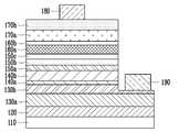
Translated fromKorean도 1a는 본 발명의 제 1 실시예에 따른 질화물 반도체 기반의 발광 소자 구조를 나타낸 단면도이다.1A is a cross-sectional view illustrating a structure of a nitride semiconductor based light emitting device according to a first embodiment of the present invention.
도 1b는 도 1a에서 p-형 금속의 위치를 달리한 질화물 반도체 기반의 발광 소자 구조를 나타낸 단면도이다.1B is a cross-sectional view illustrating a structure of a nitride semiconductor based light emitting device having different positions of p-type metals in FIG. 1A.
도 1c는 도 1a에서 p-형 금속의 위치를 달리한 질화물 반도체 기반의 발광 소자 구조를 나타낸 단면도이다.FIG. 1C is a cross-sectional view illustrating a structure of a nitride semiconductor based light emitting device having different positions of p-type metals in FIG. 1A.
도 1d는 도 1a에서 p-형 금속의 위치를 달리한 질화물 반도체 기반의 발광 소자 구조를 나타낸 단면도이다.FIG. 1D is a cross-sectional view illustrating a structure of a nitride semiconductor based light emitting device having different positions of p-type metals in FIG. 1A.
도 1e는 도 1a에서 p-형 금속의 위치를 달리한 질화물 반도체 기반의 발광 소자 구조를 나타낸 단면도이다.1E is a cross-sectional view illustrating a structure of a nitride semiconductor based light emitting device having different positions of p-type metals in FIG. 1A.
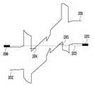
도 2a는 도 1a 내지 도 1e의 실시예의 질화물 반도체 기반의 발광소자에 대해 외부전압이 인가되지 않을 경우 전도띠 (conduction band) 및 원자가띠 (valence band) 구조를 개략적으로 나타낸 도면이다.FIG. 2A is a view schematically illustrating a conduction band and a valence band structure when an external voltage is not applied to the nitride semiconductor-based light emitting devices of the embodiments of FIGS. 1A to 1E.
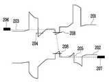
도 2b는 도 1a 내지 도 1e의 실시예의 질화물 반도체 기반의 발광소자에 대 해 발광 동작을 위해 순방향(forward)으로 외부 전압이 인가되는 경우 전도띠 (conduction band) 및 원자가띠 (valence band) 구조를 개략적으로 나타낸 도면이다.FIG. 2B illustrates a conduction band and a valence band structure when an external voltage is applied in a forward direction for the light emission operation of the nitride semiconductor based light emitting device of the embodiment of FIGS. 1A to 1E. It is a schematic drawing.
<도면의 주요 부분에 대한 부호의 설명><Explanation of symbols for the main parts of the drawings>
110 : 기판120 : 도핑되지 않은 GaN 완충 (buffer) 층110
130a : 제 1 p-형 컨택 층130b : 제 2 p-형 컨택 층130a: first p-
140a : 제 1 정공확산층140b : 제 2 정공확산층140a: first
150a : 제 1 양자우물벽층150b : 양자우물층150a: first
150c : 제 2 양자우물벽층160a : 제 2 전자확산층150c: second quantum
160b : 제 1 전자확산층170a : 제 2 n-형 컨택층160b: first
170b : 제 1 n-형 컨택층180 : n-형 금속전극170b: first n-type contact layer 180: n-type metal electrode
190 : p-형 금속전극190: p-type metal electrode
201 : 발광소자의 전도띠 끝단 (conduction-band edge)201: conduction-band edge of light emitting device
202 : 발광소자의 원자가띠 끝단 (valence-band edge)202: valence-band edge of the light emitting device
203 : 발광 동작시 페르미 에너지 준위 (Fermi energy level)203: Fermi energy level during light emission
204 : 제 1 전자확산층(160b)에 형성되는 준 2차원 전자기체의 버금띠 (subband) 에너지 준위204: Subband energy level of the quasi two-dimensional electromagnetic body formed in the first
205 : 제 1 정공확산층(140a)에 형성되는 준 2차원 정공기체의 버금띠 에너지 준위205: metal band energy level of the quasi two-dimensional hole gas formed in the first
206 : n-형 금속전극의 페르미 에너지 준위206: Fermi energy level of n-type metal electrode
207 : p-형 금속전극의 페르미 에너지 준위207: Fermi energy level of p-type metal electrode
208 : 양자우물층 (150b)에 속박된 전자의 버금띠 에너지 준위208: energy level of the electron bound in the
209 : 양자우물층 (150b)에 속박된 전공의 버금띠 에너지 준위209: Major energy level of the major bound in the
본 발명은 질화물 반도체 발광 소자에 관한 것이고, 보다 상세하게는 기판 위에 통상적으로 Ga-face로 성장된 우르짜이트 격자 구조에서 발생하는 자발 분극 및 삐에조 전기적 분극 현상으로 인한 이종접합 계면에 형성되는 준 2차원 자유전자 및 자유정공 기체를 효과적으로 이용할 수 있는 구조를 갖는 질화물 반도체 발광 소자에 관한 것이다.The present invention relates to a nitride semiconductor light emitting device, and more particularly, formed at a heterojunction interface due to spontaneous polarization and piezoelectric polarization occurring in a urethane lattice structure typically grown with Ga-face on a substrate. The present invention relates to a nitride semiconductor light emitting device having a structure capable of effectively using quasi two-dimensional free electrons and free hole gas.
질화물 반도체 (Al,In,Ga)N는 조성비에 따라 약 0.7 eV로부터 약 6.2 eV 에 이르는 넓은 에너지 영역의 밴드갭을 가지므로, 이 물질들로 구성된 이종접합구조는 가시광선 영역과 자외선 영역에서 발광하는 발광소자에 많이 응용되고 있다.Nitride semiconductors (Al, In, Ga) N have a wide bandgap of energy range from about 0.7 eV to about 6.2 eV, depending on the composition ratio, so that the heterojunction structure composed of these materials emits light in the visible and ultraviolet regions. It is widely applied to light emitting devices.
이 분야의 종래 기술은 대개 기판 위에 순차적으로 도너(donor)가 도핑된 n-형 반도체, 의도적으로 불순물로 도핑되지 않은 i-형 활성층 및 어셉터(acceptor)가 도핑된 p-형 반도체 구조가 성장된 n-i-p 구조를 이용하여 왔다.The prior art in this field usually grows n-type semiconductors sequentially donor-doped, i-type active layers not intentionally doped with impurities, and p-type semiconductor structures doped with acceptors on the substrate. Nip structure has been used.
반도체 기반의 발광소자가 높은 발광효율을 가지기 위해서는 여러 가지 중요한 요구들이 있지만, 우선적으로 n-전극으로부터 투입되는 전자와 p-전극으로부터 투입된 정공이 각기 n-형 반도체와 p-형 반도체 안에서 균일하게 확산되어 이들 두 층 사이에 형성된 활성층에서 광 전이를 통해 재결합하는 것이 필수적이다.Although semiconductor-based light emitting devices have a number of important requirements for high luminous efficiency, electrons injected from the n-electrode and holes injected from the p-electrode are uniformly diffused in the n-type semiconductor and the p-type semiconductor, respectively. And recombination via light transition in the active layer formed between these two layers is essential.
대부분의 질화물 반도체의 정공은 전자보다 이동도(mobility)가 낮기 때문에, 질화물 반도체 기반의 발광소자의 발광 특성을 향상시키기 위해서는 p-형 질화물 반도체 안에서 정공의 확산도를 높이는 것이 중요한 요구 사항들 중 하나이다. p-형 질화물 반도체의 정공의 확산도는 정공의 농도, 정공의 유효질량, 정공의 산란 센터로 작용하는 불순물의 농도 등 여러 요인들에 의존한다.Since the holes of most nitride semiconductors have lower mobility than electrons, it is one of the important requirements to increase the diffusion of holes in the p-type nitride semiconductor in order to improve light emission characteristics of the nitride semiconductor-based light emitting device. The hole diffusivity of the p-type nitride semiconductor depends on several factors, including the concentration of the hole, the effective mass of the hole, and the concentration of the impurity acting as the hole scattering center.
p-형 질화물 반도체 안에서 정공의 확산도를 높이기 위한 종래 기술은 주로 p-형 반도체의 정공의 농도를 높이는 방법이다. GaN 반도체의 경우 통상적으로 마그네슘 원자를 도핑하여 열처리하면 마그네슘 불순물이 어셉터(acceptor)로 전환되면서 자유 정공을 만들게 되어 GaN는 p-형이 된다. 이런 방법으로 통상적으로 얻을 수 있는 정공의 농도는 GaN의 경우 현재 세계최고 수준은 5 x 1017 cm-3 정도이다.The prior art for increasing the hole diffusion in the p-type nitride semiconductor is mainly a method for increasing the concentration of holes in the p-type semiconductor. In the case of GaN semiconductors, when magnesium oxide is doped and heat treated, magnesium impurities are converted into an acceptor to form free holes, and GaN becomes p-type. The hole concentration normally obtainable in this way is 5 x 1017 cm-3 for GaN.
반면 n-형 GaN 반도체는 도너(donor) 역할을 하는 실리콘 원자를 도핑하여 제작할 수 있으며 이런 방법을 통해 얻을 수 있는 자유 전자의 농도 수준은 1 x 1018cm-3 정도이다. 그러므로 n-형 GaN 반도체의 전자와 정공의 전하 농도를 비교할 때, 현재의 수준보다 발광 효율이 높은 질화물 반도체 발광소자를 구현하기 위해서는 정공의 농도를 더욱 높이거나, 정공의 이동도를 높이는 새로운 구조 개발이 요구된다.N-type GaN semiconductors, on the other hand, can be fabricated by doping silicon atoms that act as donors, and the concentration of free electrons obtained by this method is about 1 x 1018 cm-3 . Therefore, when comparing the electron and hole charge concentrations of n-type GaN semiconductors, in order to realize a nitride semiconductor light emitting device having higher luminous efficiency than the current level, a new structure for increasing the hole concentration or hole mobility is developed. Is required.
이에 본 발명자들은 발광 효율이 높은 질화물 반도체 발광 소자를 개발하기 위한 연구를 수행하면서, 기판 위에 통상적으로 Ga-face로 성장된 우르짜이트 격자 구조를 갖는 질화물 반도체 발광 소자에 있어서, 발생되는 자발분극 및 삐에로 전기적 분극 현상으로 인해 이종접합 계면에 형성되는 준 2차원 자유전자 및 자유정공 기체가 p-형 반도체 위에 n-형 반도체를 성장시키는 발광 소자 구조인 경우에 전류 확산에 효과적으로 이용될 수 있음을 발견하고 본 발명을 완성하였다. Therefore, the inventors of the present invention, while conducting research to develop a nitride semiconductor light emitting device with high luminous efficiency, spontaneous polarization and It has been found that quasi-dimensional free electrons and free hole gases formed at heterojunction interfaces due to the piercing electric polarization can be effectively used for current diffusion in the case of light emitting device structures in which n-type semiconductors are grown on p-type semiconductors. This invention was completed.
따라서, 본 발명에 따른 기술적 과제는 발광의 균일도를 개선하여 소자의 전체 발광면에서의 발광 효율을 높일 수 있도록 기판 위에 통상적으로 Ga-face로 성장된 우르짜이트 격자 구조에서 발생하는 자발 분극 및 삐에조 전기적 분극 현상으로 인해 이종접합 계면에 형성되는 준 2차원 자유전자 및 자유정공 기체를 효과적으로 이용할 수 있는 발광 구조를 갖는 질화물 반도체 발광 소자를 제공하는 것이다.Therefore, the technical problem according to the present invention is to improve the uniformity of the light emission to increase the light emission efficiency in the entire light emitting surface of the device spontaneous polarization and beep occurring in the urethane lattice structure typically grown with Ga-face on the substrate The present invention provides a nitride semiconductor light emitting device having a light emitting structure capable of effectively utilizing quasi-two-dimensional free electrons and free hole gases formed at a heterojunction interface due to an eczoelectric polarization phenomenon.
상기 기술적 과제를 해결하기 위해, 본 발명은 Ga-face로 성장된 우르짜이트 격자 구조를 갖는 질화물 반도체 발광 소자에 있어서,In order to solve the above technical problem, the present invention is a nitride semiconductor light emitting device having a Urgite lattice structure grown by Ga-face,
기판;Board;
상기 기판 상에 성장되는 완충층;A buffer layer grown on the substrate;
상기 완충층 위에 성장되는 1 p-형 컨택층;A 1 p-type contact layer grown on the buffer layer;
상기 제 1 p-형 컨택층 상에 성장되는 제 2 p-형 컨택층;A second p-type contact layer grown on the first p-type contact layer;
상기 제 2 p-형 컨택층 상에 성장되는 제 1 정공확산층:A first hole diffusion layer grown on the second p-type contact layer:
상기 제 1 정공확산층 상에 성장되는 제 2 정공확산층;A second hole diffusion layer grown on the first hole diffusion layer;
상기 제 2 정공확산층 상에 성장되는 발광활성 영역;A light emitting active region grown on the second hole diffusion layer;
상기 발광활성 영역 상에 성장되는 제 2 전자확산층;A second electron diffusion layer grown on the light emitting active region;
상기 제 2 전자확산층 상에 성장되는 제 1 전자확산층;A first electron diffusion layer grown on the second electron diffusion layer;
상기 제 1 전자 확산층 상에 성장되는 제 2 n-형 컨택층; 및A second n-type contact layer grown on the first electron diffusion layer; And
상기 제 2 n-형 컨택층 상에 성장되는 제 1 n-형 컨택층;을 포함하는 Ga-face로 성장된 우르짜이트 격자구조를 갖는 질화물 반도체 발광 소자를 제공하는 것이다.It is to provide a nitride semiconductor light emitting device having a wurtzite structure grown with a Ga-face including a first n-type contact layer grown on the second n-type contact layer.
본 발명에 따른 질화물 반도체 발광 소자에서, 상기 제 2 p-형 컨택층은 마그네슘 원자를 1 x 10¹⁸ ㎝-3 이상의 농도로 도핑한 AlxGa1-xN(0.1≤ x ≤0.5)의 조성을 갖는 물질로 성장된 것이고, 상기 제 1 정공확산층은 의도적으로 p-도핑되거나 도핑되지 않은 InyGa1-yN((0≤ y ≤0.05)의 조성을 갖는 물질로 성장되며, 의도적으로 p- 도핑되는 경우 마그네슘 원자를 1 x 10¹⁸ ㎝-3 이하의 농도로 도핑한 것이 바람직하다.In the nitride semiconductor light emitting device according to the present invention, the second p-type contact layer has a composition of Alx Ga1-x N (0.1 ≦ x ≦ 0.5) doped with magnesium atoms in a concentration of 1 × 1018 cm−3 or more. The first hole diffusion layer is grown to a material having a composition of Iny Ga1-y N ((0 ≦ y ≦ 0.05) intentionally p-doped or undoped, and intentionally p-doped. If desired, doping with magnesium atoms at a concentration of 1 × 1018 cm-3 or less is preferred.
또한, 본 발명에 따른 질화물 반도체 발광 소자에서, 상기 제 1 전자확산층은 의도적으로 n-도핑되거나 도핑되지 않은 InyGa1-yN(y는 제 2 정공확산층의 인듐 조성비와 성장기술 오차 범위 내에 있음)의 조성을 갖는 물질로 성장되며, 의도적으로 n-도핑되는 경우 실리콘 원자를 1 x 10¹⁸ ㎝-3 이하의 농도로 도핑한 것이고, 상기 제 2 n-형 컨택층은 실리콘 원자를 1 x 10¹⁸ ㎝-3 이상의 농도로 도핑한 AlxGa1-xN(x는 제 2 p-형 컨택층의 알루미늄 조성비와 성장기술 오차범위 내에 있음)의 조성을 갖는 물질로 성장된 것이 바람직하다.In addition, in the nitride semiconductor light emitting device according to the present invention, the first electron diffusion layer is intentionally n-doped or undoped Iny Ga1-y N (y is within the indium composition ratio and growth technology error range of the second hole diffusion layer And n-doped silicon atoms at a concentration of 1 x 1018 cm-3 or less, wherein the second n-type contact layer is a silicon atom of 1 x 10 It is preferably grown to a material having a composition of Alx Ga1-x N (x is in the aluminum composition ratio of the second p-type contact layer and the growth technology error range) doped at a concentration of18 cm-3 or more.
이하, 본 발명을 도면을 참조하여 상세히 설명한다.Hereinafter, the present invention will be described in detail with reference to the drawings.
도 1a는 Ga-face로 성장된 우르짜이트 격자구조를 갖는 질화물 반도체를 이용하는 본 발명의 일실시예에 따른 질화물 반도체 발광 소자의 단면도를 개략적으로 나타낸 것이다.FIG. 1A schematically illustrates a cross-sectional view of a nitride semiconductor light emitting device according to an embodiment of the present invention using a nitride semiconductor having a urethane grating structure grown with Ga-face.
도 1a을 참조하면, 본 발명의 질화물 반도체 발광 소자는 기판(110), 완충층(120), 제 1 p-형 컨택층(130a), 제 2 p-형 컨택층(130b), 제 1 정공확산층(140a), 제 2 정공확산층(140b), 제 1 양자우물벽층(150a), 양자우물층(150b), 제 2 양자우물벽층(150c), 제 2 전자확산층(160a), 제 1 전자확산층(160b), 제 2 n-형 컨택층(170a) 및 제 1 n-형 컨택층(170b)이 순차적으로 형성되며, n-형 컨택층 위에 n-형 금속전극(180)이 접촉되고, p-형 금속전극(190)은 제 2 정공확산층(140b)에 접촉시킨 구조이다.Referring to FIG. 1A, the nitride semiconductor light emitting device of the present invention includes a
상기 도 1a를 참조하여, 각 층에 대해 상세히 설명한다.Referring to FIG. 1A, each layer will be described in detail.
상기 기판(110)으로는 통상적으로 사용되는 사파이어, 실리콘카바이트 또는 GaN 기판이 사용될 수 있다.As the
상기 기판(110) 상에 도핑되지 않은 GaN 완충층(120)을 성장시킬 수 있다. GaN 완충층(120)은 0.5㎛ 내지 3㎛의 두께로 성장되는 것이 바람직하며, GaN 완충층이 격자 상수가 다른 기판을 사용할 경우 성장 온도가 낮은 저온성장 완충층과 성장온도가 상대적으로 높은 고온성장 완충층 접합구조로 구성될 수 있다.The undoped
상기 GaN 완충층(120) 위에 제 1 p-형 컨택층(130a)을 성장시킨다.The first p-
상기 제 1 p-형 컨택층(130a)은 마그네슘 원자를 1 x 1018 cm-3 이상의 농도, 바람직하게는 1 x 1018 cm-3내지 1 x 1019 cm-3의 농도로 도핑한 GaN를 이용하여 0.5 ㎛ 내지 3 ㎛의 두께로 성장하는 것이 바람직하다.The first p-
상기 제 1 p-형 컨택층(130a) 위에 제 2 p-형 컨택층(130b)을 성장시킨다.The second p-
상기 제 2 p-형 컨택층(130b)은 마그네슘 원자를 1 x 1018 cm-3 이상의 농도, 바람직하게는 1 x 1018 cm-3 내지 1 x 1019 cm-3로 도핑한 AlxGa1-xN(0.1≤ x ≤0.5)의 조성을 갖는 물질을 사용하여 5 nm 내지 50 nm의 두께로 성장되는 것이 바람직하다.The second p-
상기 제 2 p-형 컨택층(130b) 위에 제 1 정공확산층(140a)을 성장시킨다.The first
상기 제 1 정공확산층(140a)은 의도적으로 p-도핑되거나 도핑되지 않은 InyGa1-yN((0≤ y ≤0.05)의 조성을 갖는 물질을 이용하여 0.1 nm 내지 20 nm의 두께 로 성장하는 것이 바람직하다. 또한, 상기 제 1 정공확산층(140a)을 의도적으로 p-도핑하는 경우, 도핑은 마그네슘을 1 x 1018 cm-3 이하의 농도로 도핑하는 것이 바람직하다.The first
이어서, 제 1 정공확산층(140a) 위에 제 2 정공확산층(140b)을 성장시킨다.Subsequently, the second
상기 제 2 정공확산층(140b)은 마그네슘 원자를 1 x 1017 cm-3 내지 1 x 1018 cm-3의 농도로 도핑한 InzGa1-zN(0≤z≤0.05)의 조성을 갖는 물질을 이용하여 5 nm 내지 100 nm의 두께로 성장되는 것이 바람직하다.The second
상기 제 2 정공확산층(140b) 위에 발광활성 영역(150)이 성장한다. 상기 발광활성 영역(150)은 제 1 양자우물벽층(150a), 양자우물층(150b) 및 제 2 양자우물벽층(150c)으로 구분되어 성장되는 것이 바람직하다.The light emitting active region 150 is grown on the second
즉, 제 2 정공확산층(140b) 위에 제 1 양자우물벽층(150a)을 성장시킨다.That is, the first quantum
상기 제 1 양자우물벽층(150a)는 5 nm 내지 20 nm의 두께로 성장하며, 제 2 정공확산층(140b)와 같은 InzGa1-zN의 조성을 갖는 물질을 사용하되 의도적으로 도핑하지 않거나 또는 마그네슘 원자를 1 x 1017 cm-3 이하의 농도로 p-도핑하는 것이 바람직하다.The first quantum
상기 제 1 양자우물벽층(150a) 위에 양자우물층(150b)을 성장시킨다.A
상기 양자우물층(150)은 0.5 nm 내지 10 nm의 두께로 성장되며, 의도적으로 도핑하지 않은 InxGa1-xN으로 구성하되 InxGa1-xN의 밴드갭이 상기 제 1 양자우물벽층(150a) 보다 작으며, 이에 따라 인듐조성비 x의 범위는 0.05≤x≤1.0에서 한정된다.The quantum well layer 150 is grown to a thickness of 0.5 nm to 10 nm, and consists of Inx Ga1-x N which is not intentionally doped, but the band gap of Inx Ga1-x N is the first quantum well. It is smaller than the
상기 양자우물층(150b) 위에 상기 제 2 양자우물벽층(150c)을 성장시킨다.The second quantum
상기 제 2 양자우물벽층(150c)는 제 1 양자우물벽층(150a)과 같은 인듐 조성비를 갖는 InzGa1-zN 물질 및 같은 두께로 성장한다. 상기 제 2 양자우물벽층은 의도적으로 도핑하지 않거나 또는 실리콘 원자를 1 x 1017 cm-3 이하의 농도로 n-도핑한다.The second quantum
한편, 제 1 양자우물벽층(150a), 양자우물층(150b) 및 제 2 양자우물벽층(150c)으로 구성되는 단일양자우물이 1개 내지 10개의 범위 내에서 복수로 구성되는 발광활성 영역을 가질 수도 있다.On the other hand, a single quantum well composed of the first quantum
상기 제 2 양자우물벽층(150c) 위에 제 2 전자확산층(160a)을 성장시킨다.The second
상기 제 2 전자확산층(160a)은 실리콘 원자를 1 x 1017 cm-3내지 1 x 1018 cm-3 의 농도로 도핑한 InzGa1-zN의 조성을 가진 물질을 사용하여 5nm 내지 100 nm의 두께로 성장되는 것이 바람직하다. 아울러, 상기 제 2 전자확산층(160a)의 구성물질의 인듐 조성비 z는 상기 제 2 정공확산층(140b)의 인듐의 조성비와 수치적으로 성장기술 오차 범위 내에서 동일하다.The second
상기 제 2 전자확산층(160a) 위에 제 1 전자확산층(160b)을 성장시킨다.The first
상기 제 1 전자확산층(160b)는 의도적으로 n-도핑되거나 또는 도핑되지 않은 InyGa1-yN의 조성을 갖는 물질을 이용하여 0.1 nm 내지 20 nm의 두께로 성장되는 것이 바람직하며, 인듐의 조성비 y는 상기 제 1 정공확산층(140a)의 인듐 조성비와 수치적으로 성장기술 오차 범위 내에서 동일하다. 상기 제 1 전자확산층을 의도적으로 n-도핑할 경우, 도핑은 실리콘 원자를 이용하여 1 x 1018 cm-3 이하의 농도로 한다.The first
상기 제 1 전자확산층(160b) 위에 제 2 n-형 컨택층(170a)을 성장시킨다.The second n-
상기 제 2 n-형 컨택층(170a)는 실리콘 원자를 1 x 1018 cm-3 이상의 농도, 바람직하게는 1 x 1018 cm-3 내지 1 x 1019 cm-3의 농도로 도핑한 Alx Ga1-xN의 조성을 갖는 물질을 이용하여 5㎚ 내지 50㎚의 두께로 성장되는 것이 바람직하다. 이 구성 물질의 알루미늄의 조성비 x는 상기 제 2 p-형 컨택층(130b)의 알루미늄 조성비와 수치적으로 성장기술 오차 범위 내에서 동일하다.The second n-
상기 제 2 n-형 컨택층(170a) 위에 제 1 n-형 컨택층(170b)을 성장시킨다.The first n-
상기 제 2 n-형 컨택층(170b)은 실리콘 원자를 1 x 1018 cm-3 이상의 농도, 바람직하게는 1 x 1018 cm-3 내지 1 x 1019 cm-3의 농도로 도핑한 GaN를 이용하여 10 nm 내지 1 ㎛의 두께로 성장되는 것이 바람직하다.The second n-
한편, 상기 각 층들의 성장 방법은 이 분야에 일반적인 방법으로 성장될 수 있으며, 특별히 제한되지 않는다.On the other hand, the growth method of each layer may be grown in a general manner in this field, it is not particularly limited.
상기와 같은 구조의 본 발명에 따른 발광 소자는 n-형 전극(180) 및 p-형 전극(190)을 포함하며, n-형 전극(180)은 상기 제 1 n-형 컨택층(170b) 위에 접촉하며, p-형 전극(190)은 제 2 정공확산층(140a), 제 1 정공확산층(140b), 제 2 p-형 컨택층(130b) 및 제 1 p-형 컨택층(130a) 중 임의의 층을 p-전극 접촉면으로 이용할 수 있다. 또한, p-형 전극은 기판 및 GaN 완층층을 제거하여 제 1 p-형 컨택층 하부에 접촉할 수 있다. 한편, p-형 전극 접촉을 위해 성장된 구조를 통상적인 식각 방법을 통해 식각한다.The light emitting device according to the present invention having the above structure includes an n-
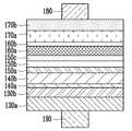
도 1b의 구조는 도 1a의 구조에서 p-형 전극(190)의 접촉면으로 제 1 정공확산층(140a)을 이용한 경우이고, 도 1c의 구조는 도 1a의 구조에서 p-형 전극(190)의 접촉면으로 제 2 p-형 컨택층(130b)을 이용한 경우이고, 도 1d의 구조는 도 1a의 구조에서 p-형 전극(190)의 접촉면으로 제 1 p-형 컨택층(130a)을 이용한 경우이다.The structure of FIG. 1B is a case in which the first
한편, 도 1e에서 제시한 구조는 도 1a의 구조에서, 기판(110)과 GaN 완충층(120)을 제거한 후, 상기 p-형 전극(190)이 제 1 p-형 컨택층(130a) 하부에 접촉한 경우를 나타낸 것이다.Meanwhile, in the structure shown in FIG. 1E, after removing the
본 발명에 따른 도 1a 내지 1e의 구조를 갖는 질화물 반도체 발광소자의 외부전압이 인가되지 않을 경우의 전도띠(conduction band) 및 원자가띠(valence band)의 구조 및 외부전압이 인가되었을 경우의 전도띠 및 원자가띠의 구조를 각각 하기 도 2a 및 도 2b에 나타내었다.Structures of the conduction band and valence band when the external voltage of the nitride semiconductor light emitting device having the structure of FIGS. 1A to 1E according to the present invention is not applied, and the conduction band when the external voltage is applied And the valence bands are shown in FIGS. 2A and 2B, respectively.
도 2a를 참조하면, 번호(201) 및 (202)로 지칭되는 것은 각각 본 발명에 따른 발광 소자의 전도띠 끝단과, 원자가띠 끝단을 나타내며, 번호(203)이 발광동작시 페르미 준위를 나타낸다. 상기 페르미 준위(203)은 제 1 p-형 컨택층의 원자가띠 끝단(202) 근방과 제 1 n-형 컨택층의 전도띠 끝단(201)을 통과해야 하는 경계조건이며, 이에 따라 밴드 모양이 결정된다. 한편, 번호(206)과 (207)로 지칭되는 것은 각각 n-형 금속전극의 페르미 에너지 준위 및 p-형 금속전극의 페르미 에너지 준위이다. 그런데, 통상적으로 사용되는 Ga-face로 성장된 우르짜이트 격자 구조를 갖는 질화물 반도체 물질을 사용하는 경우, 제 2 p-형 컨택층(130b)으로 사용되는 AlxGa1-xN의 조성을 갖는 물질 위에 InyGa1-yN의 조성을 갖는 물질이 성장하게 되면, 이들 두 물질 간의 삐에조 전기적 분극과 자발 분극의 차이로 인하여 이들 물질의 접합 계면 근방에 정공을 속박하는 버금띠(205)를 갖는 삼각 모양의 1차원 양자우물구조를 성장 축 방향으로 형성시킬 수 있고, 이 양자우물의 버금띠(205)에 속박된 정공은 성장축과 수직한 평면에서 자유롭게 움직이는 준 2차원 자유 정공 기체가 되고, 이 기체는 상대적으로 작은 산란의 효과로 인해 벌크 구조 안의 정공보다 그 이동도가 비약적으로 향상된다. 따라서, 제2 p-형 컨택층(130b) 위에 성장된 InyGa1-yN층은 정공이 평면상에서 확산하는 것으로 도모하므로 제 1 정공확산층(140a)이 된다.2A,
한편, 통상적으로 사용되는 Ga-face로 성장된 우르짜이트 격자 구조를 갖는 질화물 반도체 물질을 사용하는 경우, InyGa1-yN의 조성을 갖는 물질 위에, AlxGa1-xN 의 조성을 갖는 물질이 성장하게 되면, 이들 두 물질 간의 삐에조 전기적 분극과 자발 분극의 차이로 인하여 이들 물질의 접합 계면 근방에 전자를 속박하는 버금띠(204)를 갖는 삼각 모양의 1차원 양자우물구조가 성장 축 방향으로 형성되고, 이 양자우물의 버금띠(204)에 속박된 전자는 성장축과 수직한 평면에서 자유롭게 움직이는 준 2차원 자유 전자 기체가 되고, 이 기체는 상대적으로 작은 산란의 효과로 인해 벌크 구조안의 전자보다 그 이동도가 비약적으로 향상된다. 따라서, 제 2 n-형 컨택층(170a)과 접하고, 먼저 이 층보다 앞서 성장된 InyGa1-yN층은 전자가 평면 상에서 확산하는 것을 도모하므로 제 1 전자확산층(160b)이 된다.On the other hand, in the case of using a nitride semiconductor material having a urethane lattice structure grown with a Ga-face that is commonly used, the composition having Alx Ga1-x N on the material having a composition of Iny Ga1-y N As the material grows, a triangular one-dimensional quantum well structure with a
도 2b를 참조하면, 본 발명의 도 1a 내지 도 1e의 실시예에 따른 질화물 반도체 발광 소자에 대해 발광동작을 위해 순방향으로 외부전압을 인가했을 때 전도띠 및 원자가띠 구조를 나타낸 것이다. 본 발명의 도 1a 내지 도 1e의 실시예에 제시된 구조는 순방향으로 외부 전압이 인가되는 경우, 제 1 양자우물벽층, 양자우물층 및 제 2 양자우물벽층으로 구성되는 발광활성 영역에서 페르미 에너지 준위의 변화가 크게 나타나는 반면, 그외 다른 영역들, 즉 제 1 p-형 컨택층, 제 2 p-형 컨택층, 준 2차원 자유 정공 기체가 속박된 제 1 정공확산층, p-형의 제 2 정공확산층, n-형의 제 2 전자확산층, 준2차원 자유 전자 기체가 속박된 제 1 전자 확산층, 제 2 n-형 컨택층 및 제 1 n-형 컨택층안에서는 페르미 에너지 준위의 변화가 크지 않음을 확인할 수 있다. 이는 제 1 정공확산층과 제 1 전자확산층에 속박된 준 2차원 전하들의 밀도가 발광 동작을 위해 인가된 외부 전압에 대해 거의 의존하 지 않음을 보여주고 있다.Referring to FIG. 2B, the conductive band and valence band structures of the nitride semiconductor light emitting device according to the exemplary embodiment of FIGS. 1A to 1E are applied when an external voltage is applied in a forward direction to emit light. The structure shown in the embodiments of FIGS. 1A to 1E of the present invention is based on the Fermi energy level in the light emitting active region composed of the first quantum well wall layer, the quantum well layer and the second quantum well wall layer when an external voltage is applied in the forward direction. While the change is large, the other regions, namely the first p-type contact layer, the second p-type contact layer, the first hole diffusion layer in which the quasi-two-dimensional free hole gas is bound, and the second hole diffusion layer in the p-type , the fermi energy level does not change significantly in the n-type second electron diffusion layer, the first electron diffusion layer in which the quasi-two-dimensional free electron gas is bound, the second n-type contact layer, and the first n-type contact layer. Can be. This shows that the density of quasi-two-dimensional charges bound to the first hole diffusion layer and the first electron diffusion layer is hardly dependent on the external voltage applied for the light emission operation.
본 발명에 따른 발광 소자의 발광 동작을 설명하면, p-형 전극으로부터 투입된 정공이 제 1 정공확산층에서 성장축과 수직한 평면상에서 높은 이동성을 가지고 확산된 후, 제 2 정공확산층을 통과한 후, 발광활성 영역으로 유입되고, n-형 전극으로부터 나온 전자는 제 1 전자확산층에서 성장축과 수직한 평면상에서 높은 이동성을 가지고 확산된 후, 제 2 전자확산층을 통과한 후 발광활성 영역으로 유입되어, 발광활성 영역에서 광학적으로 재결합되어 발광하게 된다. 따라서, 본 발명의 발광 소자 구조는 발광면에서 발광의 균일도를 개선하여 소자의 전체 발광면에서 발광 효율을 개선한다.Referring to the light emitting operation of the light emitting device according to the present invention, holes injected from the p-type electrode are diffused with high mobility in the plane perpendicular to the growth axis in the first hole diffusion layer, and then pass through the second hole diffusion layer, and then emit light. The electrons introduced into the active region and diffused from the n-type electrode are diffused with high mobility in the plane perpendicular to the growth axis in the first electron diffusion layer, and then pass through the second electron diffusion layer and then enter the light emitting active region, It is optically recombined in the region to emit light. Therefore, the light emitting device structure of the present invention improves the uniformity of light emission in the light emitting surface, thereby improving the light emission efficiency in the entire light emitting surface of the device.
한편, N-face를 가지며 성장되는 질화물 반도체 구조를 이용할 경우, 본 발명에서 도 1a 내지 도 1e의 실시예와 반대순서로 성장된 구조, 즉, n-형 컨택층들이 먼저 성장하고, 그 후 순차적으로 발광활성 층들과 p-형 컨택층들이 성장한 구조를 이용함으로써 본 발명의 효과와 비슷한 결과를 얻을 수 있다.On the other hand, in the case of using a nitride semiconductor structure having an N-face, the structure grown in the reverse order to the embodiment of Figs. 1A to 1E in the present invention, that is, the n-type contact layers grow first, and then sequentially By using the structure in which the light emitting active layers and the p-type contact layers are grown, a result similar to the effect of the present invention can be obtained.
반면, Ga-face를 가지며 성장되는 질화물 반도체 구조에서, 본 발명에서 도 a 내지 도 1e의 실시예와 반대순서로 성장된 구조를 이용하는 경우, 이종접합구조상에서 분극 특성이 본 발명의 구조에서의 분극 특성과 다르기 때문에 본 발명의 효과와 같은 효과를 얻을 수 없다.On the other hand, in the nitride semiconductor structure grown with Ga-face, when the structure grown in the reverse order to the embodiment of FIGS. A to 1e is used in the present invention, the polarization characteristics on the heterojunction structure are polarized in the structure of the present invention. Since it is different from the characteristic, the effect similar to the effect of this invention cannot be acquired.
본 발명에 따른 질화물 반도체 발광소자 구조는 기판 위에 통상적으로 Ga-face로 성장된 우르짜이트 격자 구조에서 발생하는 자발 분극 및 삐에조 전기적 분 극 현상으로 인해 이종접합 계면에 형성되는 준 2차원 자유전자 및 자유정공 기체를 효과적으로 이용하는 발광 구조로서, 전극을 통해 주입된 전자와 정공이 각각의 확산층에서 높은 이동성을 가지고 성장축 방향과 수직한 평면상에서 높은 이동성을 가지고 확산하게 함으로써, 발광 소자의 발광면에서 발광의 균일도를 개선하고, 그 결과 소자의 전체 발광면에서 발광 효율을 높인다.The nitride semiconductor light emitting device structure according to the present invention is a quasi two-dimensional free form formed at a heterojunction interface due to spontaneous polarization and piezoelectric polarization phenomenon occurring in a urethane lattice structure grown with Ga-face on a substrate. A light emitting structure that effectively utilizes electrons and free hole gas, wherein electrons and holes injected through the electrode diffuse in each diffusion layer with high mobility in a plane perpendicular to the direction of growth axis, so that the light emitting surface of the light emitting device The uniformity of the light emission is improved, and as a result, the light emission efficiency is increased in the entire light emitting surface of the device.
본 발명에 따른 질화물 반도체 발광소자 구조는 준 2차원의 자유정공기체와 자유전자기체가 형성되는 제 1 정공확산층과 제 1 전자확산층이 발광활성 영역에 인접하므로, 발광동작을 위해 순방향으로 외부전압을 인가할 때, 제 2 정공확산층과 제 2 전자확산층를 통하여 발광활성 영역으로 용이하게 전하를 공급하여 발광의 효율을 높인다.In the structure of the nitride semiconductor light emitting device according to the present invention, since the first hole diffusion layer and the first electron diffusion layer in which the quasi-two-dimensional free hole gas and the free electron gas are formed are adjacent to the light emitting active region, an external voltage is applied in the forward direction for light emission operation. When applied, charge is easily supplied to the light emitting active region through the second hole diffusion layer and the second electron diffusion layer to increase the efficiency of light emission.
본 발명에 따른 질화물 반도체 발광소자는 준 2차원 자유 정공 기체가 상시 있는 제 1 정공확산층과 준 2차원 자유 전자 기체가 상시 있는 제 1 전자확산층이 발광활성영역에 인접한 곳에 있으므로 발광에 참여하지 못한 전자들이 제 1 정공 확산층을 넘어가서 소멸되는 비광학적으로 전이를 감소시킴으로써 발광의 효율을 높인다.In the nitride semiconductor light emitting device according to the present invention, since the first hole diffusion layer with the quasi two-dimensional free hole gas and the first electron diffusion layer with the quasi two-dimensional free electron gas are adjacent to the light emitting active region, By reducing the non-optical transition that disappears beyond the first hole diffusion layer, the efficiency of light emission is increased.
Claims (18)
Translated fromKoreanPriority Applications (2)
| Application Number | Priority Date | Filing Date | Title |
|---|---|---|---|
| US12/446,513US7964882B2 (en) | 2006-12-04 | 2007-10-02 | Nitride semiconductor-based light emitting devices |
| PCT/KR2007/004818WO2008069422A1 (en) | 2006-12-04 | 2007-10-02 | Nitride semiconductor-based light emitting devices |
Applications Claiming Priority (2)
| Application Number | Priority Date | Filing Date | Title |
|---|---|---|---|
| KR1020060121354 | 2006-12-04 | ||
| KR20060121354 | 2006-12-04 |
Publications (2)
| Publication Number | Publication Date |
|---|---|
| KR20080050942A KR20080050942A (en) | 2008-06-10 |
| KR100868530B1true KR100868530B1 (en) | 2008-11-13 |
Family
ID=39806094
Family Applications (1)
| Application Number | Title | Priority Date | Filing Date |
|---|---|---|---|
| KR1020070046618AActiveKR100868530B1 (en) | 2006-12-04 | 2007-05-14 | Nitride Semiconductors Based Light Emitting Devices |
Country Status (2)
| Country | Link |
|---|---|
| US (1) | US7964882B2 (en) |
| KR (1) | KR100868530B1 (en) |
Cited By (1)
| Publication number | Priority date | Publication date | Assignee | Title |
|---|---|---|---|---|
| WO2013147552A1 (en)* | 2012-03-29 | 2013-10-03 | Seoul Opto Device Co., Ltd. | Near uv light emitting device |
Families Citing this family (16)
| Publication number | Priority date | Publication date | Assignee | Title |
|---|---|---|---|---|
| DE102009054564A1 (en)* | 2009-12-11 | 2011-06-16 | Osram Opto Semiconductors Gmbh | A laser diode array and method of making a laser diode array |
| KR101051327B1 (en)* | 2010-06-09 | 2011-07-22 | 우리엘에스티 주식회사 | Group III nitride semiconductor light emitting device |
| KR101119943B1 (en)* | 2010-07-08 | 2012-03-27 | 한국과학기술연구원 | P-type semiconductor device comprising type-2 quantum well and fabrication method thereof |
| US8785904B2 (en)* | 2011-04-20 | 2014-07-22 | Invenlux Corporation | Light-emitting device with low forward voltage and method for fabricating the same |
| US8884268B2 (en)* | 2012-07-16 | 2014-11-11 | Taiwan Semiconductor Manufacturing Co., Ltd. | Diffusion barrier layer for group III nitride on silicon substrate |
| KR102075644B1 (en) | 2013-06-14 | 2020-02-10 | 엘지이노텍 주식회사 | Light emitting device, and lighting system |
| KR20140146887A (en) | 2013-06-18 | 2014-12-29 | 엘지이노텍 주식회사 | Light emitting device |
| TWI577046B (en)* | 2014-12-23 | 2017-04-01 | 錼創科技股份有限公司 | Semiconductor light emitting element and manufacturing method thereof |
| CN105914273B (en)* | 2016-05-09 | 2018-07-31 | 华灿光电(苏州)有限公司 | A kind of reddish yellow light-emitting diode epitaxial wafer and preparation method thereof |
| JP7005890B2 (en)* | 2016-10-14 | 2022-01-24 | 株式会社リコー | Semiconductor light emitting elements, lighting devices, headlights, moving objects, illumination devices, video devices, projection type video devices and projectors. |
| WO2019073413A1 (en)* | 2017-10-11 | 2019-04-18 | King Abdullah University Of Science And Technology | Semiconductor devices having heterojunctions of a boron gallium nitride ternary alloy layer and a second iii‑nitride ternary alloy layer |
| CN109346583B (en)* | 2018-08-31 | 2021-04-27 | 华灿光电(浙江)有限公司 | A kind of light-emitting diode epitaxial wafer and preparation method thereof |
| WO2022027630A1 (en)* | 2020-08-07 | 2022-02-10 | 京东方科技集团股份有限公司 | Display substrate and display device |
| CN113764554B (en)* | 2021-07-19 | 2023-08-15 | 西安电子科技大学芜湖研究院 | Light-emitting diode based on Si nanowire high-concentration p-type layer and its preparation method |
| CN114447170B (en)* | 2021-12-21 | 2023-09-19 | 华灿光电(苏州)有限公司 | LED epitaxial wafer for improving light emitting uniformity and preparation method thereof |
| CN116995169B (en)* | 2023-09-26 | 2024-04-09 | 江西兆驰半导体有限公司 | LED epitaxial wafer, preparation method thereof and LED |
Citations (2)
| Publication number | Priority date | Publication date | Assignee | Title |
|---|---|---|---|---|
| JP2005276899A (en) | 2004-03-23 | 2005-10-06 | Shin Etsu Handotai Co Ltd | Light-emitting element |
| KR20060095689A (en)* | 2005-02-28 | 2006-09-01 | 삼성전기주식회사 | Nitride semiconductor light emitting device |
Family Cites Families (9)
| Publication number | Priority date | Publication date | Assignee | Title |
|---|---|---|---|---|
| JP2809691B2 (en) | 1989-04-28 | 1998-10-15 | 株式会社東芝 | Semiconductor laser |
| US5578839A (en) | 1992-11-20 | 1996-11-26 | Nichia Chemical Industries, Ltd. | Light-emitting gallium nitride-based compound semiconductor device |
| US5959307A (en) | 1995-11-06 | 1999-09-28 | Nichia Chemical Industries Ltd. | Nitride semiconductor device |
| JP2001291895A (en) | 2000-04-06 | 2001-10-19 | Sharp Corp | Semiconductor light emitting device |
| KR20040049744A (en) | 2002-12-07 | 2004-06-12 | 한국전자통신연구원 | Heterostructure field-effect transistor |
| JP4393306B2 (en)* | 2003-10-30 | 2010-01-06 | シャープ株式会社 | Semiconductor light emitting element, method for manufacturing the same, and semiconductor device |
| JP4178410B2 (en) | 2003-11-26 | 2008-11-12 | サンケン電気株式会社 | Semiconductor light emitting device |
| US7357367B1 (en)* | 2004-04-26 | 2008-04-15 | Honeywell International, Inc. | Embedded high temperature valve |
| KR100631746B1 (en) | 2004-07-16 | 2006-10-09 | 라이프앤드엘이디 주식회사 | Manufacturing method of high brightness light emitting diode using nitride semiconductor |
- 2007
- 2007-05-14KRKR1020070046618Apatent/KR100868530B1/enactiveActive
- 2007-10-02USUS12/446,513patent/US7964882B2/ennot_activeExpired - Fee Related
Patent Citations (2)
| Publication number | Priority date | Publication date | Assignee | Title |
|---|---|---|---|---|
| JP2005276899A (en) | 2004-03-23 | 2005-10-06 | Shin Etsu Handotai Co Ltd | Light-emitting element |
| KR20060095689A (en)* | 2005-02-28 | 2006-09-01 | 삼성전기주식회사 | Nitride semiconductor light emitting device |
Cited By (1)
| Publication number | Priority date | Publication date | Assignee | Title |
|---|---|---|---|---|
| WO2013147552A1 (en)* | 2012-03-29 | 2013-10-03 | Seoul Opto Device Co., Ltd. | Near uv light emitting device |
Also Published As
| Publication number | Publication date |
|---|---|
| US20100187494A1 (en) | 2010-07-29 |
| KR20080050942A (en) | 2008-06-10 |
| US7964882B2 (en) | 2011-06-21 |
Similar Documents
| Publication | Publication Date | Title |
|---|---|---|
| KR100868530B1 (en) | Nitride Semiconductors Based Light Emitting Devices | |
| US9190567B2 (en) | Nitride semiconductor light emitting device and fabrication method thereof | |
| US6881602B2 (en) | Gallium nitride-based semiconductor light emitting device and method | |
| US8471240B2 (en) | Semiconductor layer structure with superlattice | |
| US8937325B2 (en) | Semiconductor device, wafer, method for manufacturing semiconductor device, and method for manufacturing wafer | |
| CN100583577C (en) | Nitride Semiconductor Vertical Cavity Surface Emitting Laser | |
| US20180076354A1 (en) | Ultraviolet light emitting diodes with tunnel junction | |
| US8389305B2 (en) | Techniques of forming ohmic contacts on GaN light emitting diodes | |
| KR100649496B1 (en) | Nitride semiconductor light emitting device and manufacturing method | |
| Chang et al. | Nitride-based LEDs with textured side walls | |
| EP3776671B1 (en) | Nitride based light-emitting device | |
| KR102416148B1 (en) | Micro-led including optimized passivation layer and fabricating method thereof | |
| US11658257B2 (en) | Light source assembly, optical sensor assembly, and method of manufacturing a cell of the same | |
| US9269868B2 (en) | Semiconductor light emitting element and method for manufacturing semiconductor light emitting element | |
| US11978824B2 (en) | Buried contact layer for UV emitting device | |
| Li et al. | Circular p-GaN/p-AlGaN Rods With Metal/Thin Dielectric-Type p-Contact to Increase the Wall-Plug Efficiency for 258-nm AlGaN-Based Deep Ultraviolet Light Emitting Diodes | |
| KR101056754B1 (en) | Group III nitride semiconductor light emitting device | |
| KR20140102422A (en) | Nitride-based semiconductor light emitting device | |
| KR101134063B1 (en) | Iii-nitride semiconductor light emitting device | |
| US10593839B2 (en) | Solid-state light source with small area contact | |
| KR101393914B1 (en) | Semiconductor light-emitting device and manufacturing method thereof | |
| US20140353578A1 (en) | Light-emitting device | |
| US20250228040A1 (en) | Ultrahigh efficiency excitonic device | |
| WO2008069422A1 (en) | Nitride semiconductor-based light emitting devices | |
| WO2025149575A1 (en) | Light emitting device with at least one sacrificial quantum well |
Legal Events
| Date | Code | Title | Description |
|---|---|---|---|
| A201 | Request for examination | ||
| PA0109 | Patent application | Patent event code:PA01091R01D Comment text:Patent Application Patent event date:20070514 | |
| PA0201 | Request for examination | ||
| E902 | Notification of reason for refusal | ||
| PE0902 | Notice of grounds for rejection | Comment text:Notification of reason for refusal Patent event date:20080428 Patent event code:PE09021S01D | |
| PG1501 | Laying open of application | ||
| E701 | Decision to grant or registration of patent right | ||
| PE0701 | Decision of registration | Patent event code:PE07011S01D Comment text:Decision to Grant Registration Patent event date:20081031 | |
| GRNT | Written decision to grant | ||
| PR0701 | Registration of establishment | Comment text:Registration of Establishment Patent event date:20081106 Patent event code:PR07011E01D | |
| PR1002 | Payment of registration fee | Payment date:20081107 End annual number:3 Start annual number:1 | |
| PG1601 | Publication of registration | ||
| FPAY | Annual fee payment | Payment date:20111028 Year of fee payment:4 | |
| PR1001 | Payment of annual fee | Payment date:20111028 Start annual number:4 End annual number:4 | |
| FPAY | Annual fee payment | Payment date:20120919 Year of fee payment:19 | |
| PR1001 | Payment of annual fee | Payment date:20120919 Start annual number:5 End annual number:19 |