KR100859313B1 - Method and apparatus for stable plasma processing - Google Patents
Method and apparatus for stable plasma processingDownload PDFInfo
- Publication number
- KR100859313B1 KR100859313B1KR1020050056803AKR20050056803AKR100859313B1KR 100859313 B1KR100859313 B1KR 100859313B1KR 1020050056803 AKR1020050056803 AKR 1020050056803AKR 20050056803 AKR20050056803 AKR 20050056803AKR 100859313 B1KR100859313 B1KR 100859313B1
- Authority
- KR
- South Korea
- Prior art keywords
- plasma
- substrate
- ballast
- pedestal
- chamber
- Prior art date
- Legal status (The legal status is an assumption and is not a legal conclusion. Google has not performed a legal analysis and makes no representation as to the accuracy of the status listed.)
- Expired - Fee Related
Links
Images


Classifications
- C—CHEMISTRY; METALLURGY
- C23—COATING METALLIC MATERIAL; COATING MATERIAL WITH METALLIC MATERIAL; CHEMICAL SURFACE TREATMENT; DIFFUSION TREATMENT OF METALLIC MATERIAL; COATING BY VACUUM EVAPORATION, BY SPUTTERING, BY ION IMPLANTATION OR BY CHEMICAL VAPOUR DEPOSITION, IN GENERAL; INHIBITING CORROSION OF METALLIC MATERIAL OR INCRUSTATION IN GENERAL
- C23F—NON-MECHANICAL REMOVAL OF METALLIC MATERIAL FROM SURFACE; INHIBITING CORROSION OF METALLIC MATERIAL OR INCRUSTATION IN GENERAL; MULTI-STEP PROCESSES FOR SURFACE TREATMENT OF METALLIC MATERIAL INVOLVING AT LEAST ONE PROCESS PROVIDED FOR IN CLASS C23 AND AT LEAST ONE PROCESS COVERED BY SUBCLASS C21D OR C22F OR CLASS C25
- C23F4/00—Processes for removing metallic material from surfaces, not provided for in group C23F1/00 or C23F3/00
- H—ELECTRICITY
- H01—ELECTRIC ELEMENTS
- H01L—SEMICONDUCTOR DEVICES NOT COVERED BY CLASS H10
- H01L21/00—Processes or apparatus adapted for the manufacture or treatment of semiconductor or solid state devices or of parts thereof
- H01L21/02—Manufacture or treatment of semiconductor devices or of parts thereof
- H01L21/04—Manufacture or treatment of semiconductor devices or of parts thereof the devices having potential barriers, e.g. a PN junction, depletion layer or carrier concentration layer
- H01L21/18—Manufacture or treatment of semiconductor devices or of parts thereof the devices having potential barriers, e.g. a PN junction, depletion layer or carrier concentration layer the devices having semiconductor bodies comprising elements of Group IV of the Periodic Table or AIIIBV compounds with or without impurities, e.g. doping materials
- H01L21/30—Treatment of semiconductor bodies using processes or apparatus not provided for in groups H01L21/20 - H01L21/26
- H01L21/302—Treatment of semiconductor bodies using processes or apparatus not provided for in groups H01L21/20 - H01L21/26 to change their surface-physical characteristics or shape, e.g. etching, polishing, cutting
- H01L21/306—Chemical or electrical treatment, e.g. electrolytic etching
- H01L21/3065—Plasma etching; Reactive-ion etching
- C—CHEMISTRY; METALLURGY
- C23—COATING METALLIC MATERIAL; COATING MATERIAL WITH METALLIC MATERIAL; CHEMICAL SURFACE TREATMENT; DIFFUSION TREATMENT OF METALLIC MATERIAL; COATING BY VACUUM EVAPORATION, BY SPUTTERING, BY ION IMPLANTATION OR BY CHEMICAL VAPOUR DEPOSITION, IN GENERAL; INHIBITING CORROSION OF METALLIC MATERIAL OR INCRUSTATION IN GENERAL
- C23F—NON-MECHANICAL REMOVAL OF METALLIC MATERIAL FROM SURFACE; INHIBITING CORROSION OF METALLIC MATERIAL OR INCRUSTATION IN GENERAL; MULTI-STEP PROCESSES FOR SURFACE TREATMENT OF METALLIC MATERIAL INVOLVING AT LEAST ONE PROCESS PROVIDED FOR IN CLASS C23 AND AT LEAST ONE PROCESS COVERED BY SUBCLASS C21D OR C22F OR CLASS C25
- C23F1/00—Etching metallic material by chemical means
- C23F1/08—Apparatus, e.g. for photomechanical printing surfaces
- H—ELECTRICITY
- H01—ELECTRIC ELEMENTS
- H01J—ELECTRIC DISCHARGE TUBES OR DISCHARGE LAMPS
- H01J37/00—Discharge tubes with provision for introducing objects or material to be exposed to the discharge, e.g. for the purpose of examination or processing thereof
- H01J37/32—Gas-filled discharge tubes
- H01J37/32009—Arrangements for generation of plasma specially adapted for examination or treatment of objects, e.g. plasma sources
- H01J37/32082—Radio frequency generated discharge
- H01J37/321—Radio frequency generated discharge the radio frequency energy being inductively coupled to the plasma
- H—ELECTRICITY
- H01—ELECTRIC ELEMENTS
- H01J—ELECTRIC DISCHARGE TUBES OR DISCHARGE LAMPS
- H01J37/00—Discharge tubes with provision for introducing objects or material to be exposed to the discharge, e.g. for the purpose of examination or processing thereof
- H01J37/32—Gas-filled discharge tubes
- H01J37/32431—Constructional details of the reactor
- H01J37/32623—Mechanical discharge control means
- H01J37/32633—Baffles
- H—ELECTRICITY
- H01—ELECTRIC ELEMENTS
- H01L—SEMICONDUCTOR DEVICES NOT COVERED BY CLASS H10
- H01L21/00—Processes or apparatus adapted for the manufacture or treatment of semiconductor or solid state devices or of parts thereof
- H01L21/67—Apparatus specially adapted for handling semiconductor or electric solid state devices during manufacture or treatment thereof; Apparatus specially adapted for handling wafers during manufacture or treatment of semiconductor or electric solid state devices or components ; Apparatus not specifically provided for elsewhere
- H01L21/67005—Apparatus not specifically provided for elsewhere
- H01L21/67011—Apparatus for manufacture or treatment
- H01L21/67017—Apparatus for fluid treatment
- H01L21/67063—Apparatus for fluid treatment for etching
- H01L21/67069—Apparatus for fluid treatment for etching for drying etching
Landscapes
- Engineering & Computer Science (AREA)
- Chemical & Material Sciences (AREA)
- Physics & Mathematics (AREA)
- Plasma & Fusion (AREA)
- Analytical Chemistry (AREA)
- Organic Chemistry (AREA)
- Metallurgy (AREA)
- Mechanical Engineering (AREA)
- Materials Engineering (AREA)
- General Physics & Mathematics (AREA)
- Power Engineering (AREA)
- Microelectronics & Electronic Packaging (AREA)
- Computer Hardware Design (AREA)
- Manufacturing & Machinery (AREA)
- Condensed Matter Physics & Semiconductors (AREA)
- Chemical Kinetics & Catalysis (AREA)
- General Chemical & Material Sciences (AREA)
- Drying Of Semiconductors (AREA)
- Plasma Technology (AREA)
Abstract
Translated fromKorean
Description
Translated fromKorean도 1은 플라즈마 안정기를 갖는 에칭 반응기의 개략도이다.1 is a schematic diagram of an etching reactor having a plasma ballast.
도 2는 도 1의 플라즈마 안정기의 일 실시예에 대한 부분 등각도이다.FIG. 2 is a partial isometric view of one embodiment of the plasma ballast of FIG. 1.
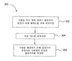
도 3은 텅스텐을 에칭하는 방법의 흐름도이다.3 is a flow chart of a method of etching tungsten.
* 도면의 주요 부분에 대한 부호의 설명 *Explanation of symbols on the main parts of the drawings
100: 반응기 102: 처리 챔버100: reactor 102: processing chamber
108: 천정부 112: 플라즈마 전력원108: ceiling 112: plasma power source
122: 기판 124: 패데스탈122: substrate 124: pedestal
178: 상부 처리 볼륨 180: 하부 처리 볼륨178: upper processing volume 180: lower processing volume
일반적으로 본 발명의 실시예들은 기판의 플라즈마 처리 방법 및 장치에 관한 것으로서, 특히, 안정된 플라즈마를 사용하여 기판을 에칭하는 방법 및 장치에 관한 것이다.In general, embodiments of the present invention relate to a method and apparatus for plasma processing a substrate, and more particularly, to a method and apparatus for etching a substrate using a stable plasma.
집적 회로는 단일 칩 상에 수 백만개의 트랜지스터, 커패시터 및 저항기를 갖는 복잡한 소자들에 포함된다. 칩 구조는 보다 빠른 회로와 보다 많은 회로 밀도를 갖도록 계속해서 요구되면서 발전하였다. 회로 밀도는 회로가 실행될 수 있는 기능의 속도와 수가 회로 구조물의 밀도에 따라 증가하기 때문에 회로 밀도가 중요하다는 것은 공지된 사실이다. 집적 회로의 속도와 회로 밀도에 영향을 주는 일부 구조 특성은 기판 상에 형성된 회로 구조물을 포함한 층을 형성하는데 사용된 재료의 저항과 두께를 포함한다.Integrated circuits are involved in complex devices with millions of transistors, capacitors and resistors on a single chip. Chip structures have evolved to continue to be required to have faster circuits and more circuit densities. It is well known that circuit density is important because the circuit density increases with the density of the circuit structure, as the speed and number of functions that the circuit can execute is increased. Some structural properties that affect the speed and circuit density of integrated circuits include the resistance and thickness of the materials used to form the layers, including circuit structures formed on the substrate.
금속 재료는 와이어라인 상호접속부, 비아, 전극 등과 같은 회로 구조물을 형성하는데 사용된다. 금속 구조물은 집적 회로의 기능성에 중요하다. 회로 구조물을 제조하는데 종종 사용되는 금속은 텅스텐이다. 텅스텐은 종래 화학 기상 증착(CVD) 방법을 사용하여 정확하게 증착될 수 있고 낮은 저항성을 갖는다. 회로 설계자는 텅스텐이 폴리실리콘의 침투에 양호한 저항성을 나타내고, 이는 기판 처리 및 소자 사용 과정 중에 텅스텐이 물리적 특성을 보유할 수 있기 때문에 텅스텐이 근사한 폴리실리콘을 사용하기에 바람직한 재료라는 것을 안다.Metallic materials are used to form circuit structures such as wireline interconnects, vias, electrodes, and the like. Metal structures are important for the functionality of integrated circuits. The metal often used to make circuit structures is tungsten. Tungsten can be deposited accurately using conventional chemical vapor deposition (CVD) methods and has low resistance. Circuit designers know that tungsten exhibits good resistance to infiltration of polysilicon, which is a preferred material for using tungsten approximated polysilicon because tungsten can retain its physical properties during substrate processing and device usage.
회로 밀도를 최대화시키기 위해, 텅스텐과 같은 것을 갖는 회로 구조물을 포함하는 층은 최소가 되어야 한다. 그러나, 이러한 얇은 층을 처리할 때, 처리 동안 층이 손상되는 것을 방지하도록 주의해야 한다. 손상된 층은 회로 구조물에 결함을 유발하고 기판 폐기율(reject)을 증가시킨다.In order to maximize circuit density, the layer containing the circuit structure having something like tungsten should be minimal. However, when treating such thin layers, care must be taken to prevent damage to the layers during the treatment. Damaged layers cause defects in circuit structures and increase substrate rejects.
얇은 층에 쉽게 손상을 줄 수 있는 처리가 에칭이다. 플루오린 화학제는 통상적으로 노출된 텅스텐 및 기타 금속을 제거하는데 사용된다. 플라즈마는 에칭 처리를 향상시키는데 사용될 수 있다. 그러나, 안정된 플라즈마를 유지시키는 것은 어렵다. 플라즈마 안정성을 높이는 한가지 방법은 챔버에 공급된 전력을 높이는 것이다. 또 다른 방법은 에칭되는 기판과 챔버 상부 간의 갭을 감소시키는 것이다. 불행히도, 전력 증가와 갭 감소는 기판의 이온 충격을 증가시키고, 이는 기판 상에 형성된 회로에 심각한 손상을 줄 수 있다.Etching is a process that can easily damage thin layers. Fluorine chemicals are commonly used to remove exposed tungsten and other metals. Plasma can be used to enhance the etching process. However, it is difficult to maintain a stable plasma. One way to increase plasma stability is to increase the power supplied to the chamber. Another method is to reduce the gap between the substrate being etched and the chamber top. Unfortunately, increased power and reduced gap increase the ion bombardment of the substrate, which can seriously damage circuits formed on the substrate.
따라서, 기판 상에 재료를 에칭하기 위한 개선된 방법 및 장치를 위한 기술이 필요하다.Accordingly, there is a need for techniques for improved methods and apparatus for etching materials on substrates.
본 발명은 일반적으로 공간적으로 변형된 플라즈마를 사용하여 기판을 에칭하기 위한 방법과 장치를 제공한다. 일 실시예에서, 본 방법은 기판 지지 패데스탈 상에 위치한 플라즈마 안정기를 갖는 처리 챔버를 제공하는 단계를 포함한다. 기판은 패데스탈 상에 위치한다. 처리 가스는 처리 챔버 안으로 유입되고 플라즈마는 처리 가스로부터 형성된다. 기판은 플라즈마 안정기에 의해 한정된 소정의 이온 밀도 대 라디칼 밀도 비를 갖는 플라즈마에 의해 에칭된다.The present invention generally provides a method and apparatus for etching a substrate using a spatially modified plasma. In one embodiment, the method includes providing a processing chamber having a plasma ballast located on a substrate support pedestal. The substrate is located on the pedestal. Process gas is introduced into the process chamber and plasma is formed from the process gas. The substrate is etched by a plasma having a predetermined ion density to radical density ratio defined by a plasma ballast.
본 발명의 또 다른 실시예에서, 장치는 공간적으로 변형된 플라즈마를 갖는 기판을 에칭하기 위해 제공된다. 본 장치는 내부에 배치된 기판 지지 패데스탈을 갖는 처리 챔버를 포함한다. RF 전력 소스는 챔버에 플라즈마를 형성하기 위해 제공된다. 플라즈마 안정기는 패데스탈 위의 챔버 내에 배치된다. 플라즈마 안정기는 플라즈마의 전하와 중성 종의 공간 분포를 제어한다. 플라즈마 안정기는 챔버로부터 전기적으로 절연된 거의 평탄한 부재를 포함할 수 있다. 상기 부재는 관통 되게 형성된 다수의 개구부를 갖는다.In another embodiment of the present invention, an apparatus is provided for etching a substrate having a spatially modified plasma. The apparatus includes a processing chamber having a substrate support pedestal disposed therein. An RF power source is provided to form a plasma in the chamber. The plasma ballast is disposed in the chamber above the pedestal. The plasma ballast controls the charge of the plasma and the spatial distribution of the neutral species. The plasma ballast may include a substantially flat member that is electrically insulated from the chamber. The member has a plurality of openings formed therethrough.
상기 언급한 본 발명의 특징이 더 상세히 이해될 수 있도록, 이미 간략히 요약한 본 발명의 상세한 설명이 실시예들을 참조로 이루어지며, 이들 실시예 중 일부는 첨부된 도면에 도시되어 있다. 그러나, 첨부된 도면은 단지 본 발명의 통상적인 실시예들만을 도시하며 본 발명의 범위를 제한하지 않으며, 동일한 효과를 발휘하는 다른 실시예들이 구현될 수 있다.BRIEF DESCRIPTION OF DRAWINGS In order that the above-mentioned features of the present invention may be understood in more detail, a detailed description of the present invention which has been briefly summarized is made with reference to the embodiments, some of which are illustrated in the accompanying drawings. However, the appended drawings show only typical embodiments of the present invention and do not limit the scope of the present invention, and other embodiments may be implemented that achieve the same effect.
본 발명은 개선된 에칭 처리의 방법과 장치를 제공한다. 상기 장치는 플라즈마 처리 챔버 내에 배치된 플라즈마 안정기를 포함한다. 플라즈마 안정기는 밀집되고 안정된 플라즈마가 (플라즈마 안정기 위의) 챔버의 상부 처리 영역에 형성되고 플라즈마가 (플라즈마 안정기와 기판 지지 패데스탈 상에 배치된 기판 사이의) 하부 처리 영역에서 제어된 특성을 갖도록 처리 동안 챔버의 전하와 중성 종의 공간 분포를 제어한다.The present invention provides a method and apparatus for improved etching treatment. The apparatus includes a plasma ballast disposed in a plasma processing chamber. The plasma ballast is treated such that a dense and stable plasma is formed in the upper processing area of the chamber (above the plasma ballast) and the plasma has controlled properties in the lower processing area (between the plasma ballast and the substrate disposed on the substrate support pedestal). While controlling the charge of the chamber and the spatial distribution of the neutral species.
도 1은 플라즈마 안정기(170)를 갖는 에칭 반응기(100)의 개략적인 도이다. 여기서 개시된 설명과 함께 사용되기에 적합할 수 있는 적절한 반응기는 예컨대 디커플드 플라즈마 소스(DSP®)Ⅰ 및 DSP®Ⅱ 반응기를 포함하며, 이들 모두는 캘리포니아, 산타 클라라의 어플라이드 머티어리얼스사로부터 이용할 수 있다. 또한 DSP®Ⅰ 및 DSP®Ⅱ 반응기는 센츄라® 집적 반도체 웨이퍼 처리 시스템의 처리 모듈로서 사용될 수 있으며, 이는 역시 어플라이드 머티어리얼스사로부터 이용할 수 있다. 여기서 개시된 반응기(100)의 특정 실시예는 예시적인 목적을 위해 제공되고 본 발 명의 범위를 제한하지 않는다.1 is a schematic diagram of an
일반적으로 반응기(100)는 도전성 몸체(벽)(104) 내의 기판 페데스탈(124)을 갖는 처리 챔버(102), 및 제어기(146)를 포함한다. 챔버(102)는 거의 평탄한 유전성 천정부(108)를 갖는다. 챔버(102)의 다른 실시예들은 다른 타입의 천정부, 예컨대 돔-형상의 천정부를 가질 수 있다. 안테나(110)는 천정부(108) 위에 배치된다. 안테나(110)는 선택적으로 제어될 수 있는 하나 이상의 유전성 코일 부재를 포함한다(두 개의 동일축 부재(110a 및 110b)가 도 1에 예시적으로 도시되어 있다). 안테나(110)는 제 1 매칭 네트워크(114)를 통해 플라즈마 전력원(112)에 결합된다. 플라즈마 전력원(112)은 통상적으로 약 50kHz 내지 약 13.56 MHz 범위의 조정가능한 주파수에서 약 3000W까지 발생시킬 수 있다.
기판 패데스탈(캐소드)(124)는 제 2 매칭 네트워크(142)를 통해 바이어싱 전력원(140)에 결합된다. 바이어싱 전력원(140)은 일반적으로 연속 또는 펄스 전력을 발생시킬 수 있는 대략 13.56 MHz의 주파수에서 대략 500W까지의 전력을 발생시키는 전력원이다. 선택적으로, 전력원(140)은 DC 또는 펄스 DC 전력원일 수 있다.The substrate pedestal (cathode) 124 is coupled to the
일 실시예에서, 기판 지지 패데스탈(124)은 정전기 척(160)을 포함한다. 정전기 척(160)은 적어도 하나의 클램핑 전극(132)을 포함하고 척 전력 공급기(166)에 의해 제어된다. 선택적인 실시예에서, 기판 패데스탈(124)은 서셉터 클램프 링, 기계적인 척 등과 같은 기판 지지 메커니즘을 포함할 수 있다.In one embodiment, the
리프트 메커니즘(138)은 기판 지지 패데스탈(124) 위로 또는 떨어져서 기판(122)을 상승 및 하강시키는데 사용된다. 일반적으로, 리프트 메커니즘(162)은 각 각의 가이드 홀(136)을 통해 이동하는 다수의 리프트 핀(130)(하나의 리프트 핀이 도시됨)을 포함한다.
동작시, 기판(122)의 온도는 기판 패데스탈(124)의 온도를 안정화시킴으로써 제어된다. 일 실시예에서, 기판 지지 패데스탈(124)은 저항성 히터(144)와 열 싱크(128)를 포함한다. 저항성 히터(144)는 일반적으로 적어도 하나의 가열 부재(134)를 포함하고 히터 전력 공급기(168)에 의해 조절된다. 가스 소스(156)로부터의 후방 가스(즉, 헬륨)은 가스 콘딧(158)을 통해 기판(122) 아래의 패데스탈 표면에 형성된 채널에 제공된다. 후방 가스는 패데스탈(124)과 기판(122) 사이의 열 전달을 촉진시키는데 사용된다. 처리 동안, 패데스탈(124)은 내장된 저항성 히터(144)에 의해 안정-상태 온도까지 가열될 수 있으며, 이는 헬륨 후방 가스와 결합하여 기판(122)의 균일한 가열을 촉진시킨다. 이러한 열 제어를 이용하여, 기판(122)은 약 0 내지 350 섭씨온도 사이에서 유지될 수 있다.In operation, the temperature of the substrate 122 is controlled by stabilizing the temperature of the
플라즈마 안정기(170)는 패데스탈(124) 상의 챔버(102) 내에 배치된다. 플라즈마 안정기(170)는 처리 동안 챔버(102)전하 및 중성 종의 공간 분포를 제어하고, 이로써 (플라즈마 안정기(170) 위의) 챔버의 상부 처리 영역에 밀집되고 안정된 플라즈마를 제공하며 플라즈마가 (플라즈마 안정기(170)와 기판 지지 패데스탈(124) 상에 배치된 기판(122) 사이의) 하부 처리 영역에서 제어된 특성을 갖게 한다.
플라즈마 안정기(170)는 챔버 벽(104)과 패데스탈(124)로부터 전기적으로 절연되고 일반적으로 거의 평탄한 플레이트(172)와 다수의 레그(176)를 포함한다. 플레이트(172)는 챔버(102) 내에서 레그(176)에 의해 패데스탈(124) 위에서 지지된다. 플레이트(172)는 플레이트(172)의 표면에서 원하는 개방 영역을 형성하는 하나 이상의 개구부(애퍼쳐)를 형성한다. 플라즈마 안정기(170)의 개방 영역은 처리 챔버(102)의 상부 처리 볼륨(178)에 형성된 플라즈마로부터 플라즈마 안정기(170)와 기판(122) 사이에 위치한 하부 처리 볼륨(180)까지 이동하는 이온의 양을 제어한다. 따라서, 플라즈마 안정기(170)의 개방 영역은 처리 챔버(102)의 플라즈마의 전하 및 중성 종의 공간 분포를 제어한다. 개방 영역이 클수록, 많은 이온이 플라즈마 안정기(170)를 통과할 수 있다. 이와 같이, 애퍼쳐(174)의 크기는 볼륨(180) 내의 이온 밀도에 영향을 미친다.The
또한 플라즈마 안정기(170)의 애퍼쳐(174), 또는 개방 영역은 RF 전력이 플라즈마로 제공되는 처리 챔버(102)의 상부 처리 볼륨(178) 내로의 확산으로부터 형성된 기판(122)의 표면 상의 에칭 부산물의 양에 영향을 준다. 애퍼쳐(174)의 크기는 상부 처리 볼륨(178)에 형성된 충분한 이온과 라디칼이 기판(122)의 표면에 도달하게 하고 에칭 부산물이 RF 전력의 플라즈마로의 제공을 현저히 불안정하게 하지 않게 하도록 선택된다.The
게다가, 개방 영역이 클수록, 플라즈마의 전하 및 중성 종의 공간 분포가 더 균일해진다. 또한 큰 개방 영역일수록 플라즈마의 안정성을 감소시킨다. 따라서, 플라즈마 안정기(170)의 개방 영역을 제어함으로써, 플라즈마의 안정성이 제어된다. 게다가, 상부 및 하부 처리 볼륨(178,180)의 전하 및 중성 종의 공간 분포가 제어되고, 이로써 에칭 균일성과 선택도를 제어한다.In addition, the larger the open area, the more uniform the spatial distribution of charge and neutral species in the plasma. The larger open area also reduces the stability of the plasma. Therefore, by controlling the open area of the
도 2는 플라즈마 안정기(170)의 특정 실시예를 도시한다. 본 실시예에서, 플라즈마 안정기(170)는 하나 이상의 애퍼쳐(174)와 다수의 레그(176)를 갖는 플레이트(172)를 포함한다. 플레이트(172)는 견고할 정도로 충분히 두꺼워야 하고 플라즈마에 형성된 이온이 재결합하는 것을 방지할 정도로 충분히 얇아야 한다. 플레이트(172)는 (알루미나와 같은) 세라믹, 석영, 양극산화된 알루미늄, 또는 처리 화학제 및 조건과 호환가능한 기타 재료들로 제조될 수 있다. 또 다른 실시예에서, 플레이트(172)는 스크린 또는 메시(mesh)를 포함할 수 있으며, 스크린 또는 메시의 개방 영역은 하나 이상의 애퍼쳐(174)에 의해 제공된 원하는 개방 영역에 대응한다. 선택적으로, 플레이트 및 스크린 또는 메시의 조합이 이용될 수도 있다.2 illustrates a particular embodiment of the
하나 이상의 애퍼쳐(174)는 원하는 개방 영역을 얻기 위해 크기, 이격 및 플레이트(172)의 표면을 가로지른 기하학적 배치가 바뀔 수 있다. 애퍼쳐(174)는 플라즈마가 플레이트(172)를 충분히 관통할 수 있을 정도로 충분히 커야하고 플레이트(172)의 표면에서 대략 2 퍼센트 내지 대략 90 퍼센트의 개방 영역을 형성하도록 배치될 수 있다. 일 실시예에서, 애퍼쳐(174)는 직경이 0.2인치(0.51cm) 보다 크다. 일 실시예에서, 하나 이상의 애퍼쳐(174)는 정사각형 그리드 패턴에 배치된 직경이 대략 1/2인치(1.25cm)인 다수의 홀을 포함한다. 홀은 다른 크기의 홀 또는 다양한 크기의 홀을 이용한 기타 기하학적 또는 임의의 패턴으로 배치될 수 있다. 또 다른 실시예에서, 하나 이상의 애퍼쳐(220)는 하나의 애퍼쳐(220)를 포함할 수 있다. 일 실시예에서, 하나의 애퍼쳐(220)는 실질적으로 패데스탈(616) 상에 배치된 기판(614)의 동일한 크기와 모양을 가질 수 있다.One or
홀의 크기, 모양 및 패턴은 하부 처리 볼륨(180)의 원하는 이온 밀도에 따라 바뀔 수 있다. 예컨대, 작은 직경의 더 많은 홀들이 볼륨(180)의 라디칼대 이온 밀도 비율을 높이는데 사용될 수 있다. 다른 경우에, 홀은 더 크거나, 다수의 던 큰 홀들이 볼륨(180) 내의 이온 밀도 대 라디칼 밀도 비율을 높이기 위해 작은 홀들과 혼합되어 사용될 수 있다. 선택적으로, 더 큰 홀들이 볼륨(180)의 이온 분포와 동일한 윤곽을 이루기 위해(contour) 플레이트(174)의 특정 영역에 위치할 수 있다. 또한, 홀은 플레이트 표면에 수직이 아닐 수 있으며, 즉 이들이 비스듬한 각을 가질 수 있다.The size, shape, and pattern of the holes may vary depending on the desired ion density of the
플라즈마 안정기(170)가 지지되는 높이는 에칭 처리를 더욱 잘 제어하기 위해 바뀔 수 있다. 플라즈마 안정기(170)가 천정부(108)에 인접하여 위치할 수록, 상부 처리 볼륨(178)은 더 작아진다. 보다 작은 상부 처리 볼륨(178)은 더욱 안정된 플라즈마를 형성한다. 일 실시예에서, 플라즈마 안정기(170)는 천정부(108)로부터 대략 1 인치(2.54cm)에 배치된다. 보다 빠른 에칭 속도는 패데스탈(124)과 기판에 더욱 인접하게 플라즈마 안정기(170)를 위치시킴으로써 얻어질 수 있다. 선택적으로, 하부의 더욱 잘 제어된 에칭 속도는 패데스탈(124)과 더욱 멀리 플라즈마 안정기(170)를 위치시킴으로써 얻어질 수 있다. 일 실시예에서, 플라즈마 안정기(170)는 패데스탈(124)로부터 대략 2 인치에 위치한다. 선택적으로, 플라즈마 안정기(170)는 임의의 영역으로 및 더 먼 다른 영역으로 천정부(108)에 더욱 인접하도록 동일한 윤곽을 이루는 모양을 가질 수 있으며, 이로써 플라즈마의 모양과 윤곽을 제어하기에 바람직한 방식으로 처리 챔버(102)의 상부 볼륨(178)을 형상화 시킨다.The height at which the
기판(122)과 관련하여 이격된 관계로 플레이트(172)를 유지시키기 위해, 플레이트(172)는 패데스탈(124) 상에 배치된 다수의 레그(176)에 의해 지지된다. 레그(176)는 일반적으로 패데스탈(124) 또는 에지 링(126)의 외부 둘레 주위에 위치하고 플레이트(172)와 동일한 재료로 제조될 수 있다. 일 실시예에서, 레그(176)는 플라즈마 안정기(170)를 위해 안정된 지지를 제공하는데 사용될 수 있다. 일반적으로, 레그(176)는 기판(122) 도는 패데스탈(124)과 관련하여 거의 평행한 방향으로 플레이트(172)를 유지시킨다. 그러나, 비스듬한 각도의 방향은 레그(176)의 길이를 변화시킴으로써 사용될 수 있다.In order to maintain the
레그(176)의 상단부는 플레이트(172)에 형성된 대응하는 홀에 가압되어 끼워질 수 있다. 선택적으로, 레그(176)의 상단부는 플레이트(172) 또는 브래킷에 스레디드되어 플레이트(172)의 하부에 고정될 수 있다. 처리 조건과 모순되지 않는 기타 종래의 고정 방법이 레그(176)를 플레이트(172)에 고정하는데 사용될 수 있다.The upper end of the
레그(176)는 패데스탈(124) 또는 에지 링(126)에 놓여질 수 있다. 선택적으로, 레그(176)는 패데스탈(124) 또는 에지 링(126)에 형성된 수용 홀(도시 안됨) 안으로 연장할 수 있다. 또한 나사, 볼트, 접합 등과 같은 기타 고정 방법이 플라즈마 안정기(170)를 패데스탈(124) 또는 에지 링(126)에 고정하기 위해 고려된다. 에지 링(126)에 고정될 때, 플라즈마 안정기(170)는 사용, 유지, 교체 등이 용이하게-교체가능한 처리 키트의 일부일 수 있다. 플라즈마 안정기(170)는 처리 챔버 내에서 용이하게 개장되도록(retrofit) 고려될 수 있다.
선택적으로, 플레이트(172)는 - 플레이트(172)가 접지 경로와 절연되는 한 - 처리 챔버(102)의 벽(104) 또는 기타 구조물에 부착된 브래킷(도시 안됨)을 사용하는 것과 같은 기타 수단에 의해 패데스탈(124) 위에서 지지될 수 있다.Optionally,
도 1을 참조하면, 하나 이상의 처리 가스가 가스 판넬(120)로부터 처리 챔버(102)에 제공된다. 통상적으로 처리 가스는 기판 패데스탈(124) 위에 위치한 하나 이상의 주입구(116)(즉, 개구부, 분사기 등)을 통해 공급된다. 도 1에 도시된 실시예에서, 처리 가스는 환형 가스 채널(118)을 사용하여 주입구(116)에 제공된다. 가스 채널(118)은 벽(104)에 결합된 (도시된 바와 같은) 가스 링에 또는 벽(104)에 형성될 수 있다. 에칭 처리 동안, 처리 가스는 플라즈마 소스(112)로부터 안테나(110)로 전력을 공급함으로써 플라즈마로 점화된다.Referring to FIG. 1, one or more process gases are provided from the
챔버(102)의 압력은 스로틀 밸브(162)와 진공 펌프(164)를 사용하여 제어된다. 벽(104)의 온도는 벽(104)을 통해 연장하는 액체-함유 콘딧(도시 안됨)을 사용하여 제어될 수 있다. 통상적으로, 챔버 벽(104)은 금속(즉, 알루미늄, 스테인레스 강 등)으로 제조되며 전기적 접지(106)에 결합된다. 또한 처리 챔버(102)는 처리 제어, 내부 진단, 종료점 검출 등을 위해 종래 시스템을 포함한다. 이러한 시스템은 지원 시스템(154)으로서 집합적으로 도시되어 있다.The pressure in
제어기(146)는 중앙 처리 유닛(CPU)(644), 메모리(148), CPU(150)를 위한 지원 회로(152)를 포함하며 처리 챔버(102)의 부품 및 에칭 처리의 제어를 용이하게 하며, 이는 이하에서 더 상세히 설명한다. 제어기(146)는 다양한 챔버 및 하위-프 로세서를 제어하기 위해 산업 설비에 사용될 수 있는 범용 컴퓨터 프로세서의 형태중 하나일 수 있다. CPU(150)의 메모리 또는 컴퓨터-판독가능 매체(642)는 랜덤 액세스 메모리(RAM), 리드 온리 메모리(ROM), 플로피 디스크, 하드 디스크 또는 기타 부분적인 또는 원격의 디지털 기억장치의 형태와 같이 용이하게 이용가능한 하나 이상의 메모리일 수 있다. 지원 회로(152)는 종래 방식으로 프로세서를 지원하기 위해 CPU(150)에 결합된다. 이들 회로는 캐시, 전력 공급기, 클럭 회로, 입/출력 회로 및 하위 시스템 등을 포함한다. 본 발명의 방법은 일반적으로 소프트웨어 루틴과 같이 메모리(148)에 저장된다. 선택적으로, 이러한 소프트웨어 루틴은 CPU(150)에 의해 제어되는 하드웨어로부터 원격으로 위치한 제 2 CPU(도시 안됨)에 의해 저장 및/또는 실행될 수 있다.
기판 상에 배치된 텅스텐 층을 에칭하기 위해 플라즈마 안정기(170)를 사용하는 예시적인 방법(300)이 도 3의 흐름도에 도시되어 있으며 도 1을 참조로 설명된다. 방법(300)은 기판(122)이 플라즈마 안정기(170) 바로 아래의 지지 패데스탈(124) 상의 처리 챔버(102)에 위치하는 단계(302)에서 시작한다. 기판(122)은 기판 상에 위치한 적어도 부분적으로 노출된 텅스텐 층을 갖는 반도체 기판이다. 대략 0 내지 200W의 바이어스 전력은 처리 동안 패데스탈(124) 상의 적절한 위치에서 기판(124)의 지지를 돕기 위해 바이어스 전력원(140)에 의해 공급될 수 있다. 일 실시예에서, 대략 50W의 바이어스 전력이 공급된다. 비록 텅스텐이 본 발명의 플라즈마 안정기(170)를 사용하여 유리하게 에칭될 수 있는 재료중 일 예로서 설명되었지만, 다른 재료들, 특히 금속이 안정기(170)와 이에 의해 생성된 플라즈마를 이 용하여 유리하게 에칭될 수 있다.An
단계(304)에서, 처리 가스는 처리 챔버(102) 안으로 유입된다. 처리 가스는 설퍼 헥사플루오라이드(SF6)일 수 있으며 나이트로겐(N2)을 포함할 수 있다. SF6는 분당 약 20 내지 300 표준 입방 센티미터(sccm)의 속도로 제공될 수 있다. 일 실시예에서, SF6는 약 48 sccm의 속도로 제공된다. N2는 약 0 내지 약 30 sccm의 속도로 제공될 수 있다. 일 실시예에서, N2는 약 12 sccm의 속도로 제공된다. 에칭을 위한 기타 적절한 가스는 클로린(Cl2), 나이트로겐 트리플루오라이드(NF3), 카본 테트라플로오라이드(CF4), 하이드로겐 클로라이드(HCl) 등을 포함한다. 이들 처리 가스는 SF6와 같이 유사한 범위에서 제공될 수 있으며 가스 혼합물의 일부이거나 N2와 같은 기타 처리 가스와 함께 유입될 수 있다. 처리 챔버(102) 내부의 압력은 약 3 내지 약 50 mTorr의 범위에 있도록 제어된다. 일 실시예에서, 처리 챔버(102) 내부의 압력은 약 10 mTorr가 되도록 제어된다.In
단계(306)에서, 플라즈마는 플라즈마 전력원(112)으로부터 안테나(110)까지 RF 전력을 공급함으로써 챔버(102)에 형성된다. 통상적으로 전력은 약 100 내지 약 1200W의 범위에서 제공된다. 일 실시예에서, 약 600W의 전력 레벨에서의 RF 전력은 약 13.56 MHz의 주파수로 안테나(110)에 제공된다.In
플라즈마가 단계(306) 동안 형성될 때, 플라즈마 안정기(170)는 상부 처리 볼륨(178) 내에서 밀집되고 안정된 플라즈마를 제공한다. 따라서, 기판(122)을 낮은 압력과 전력 조건에서 에칭되게 하는 것이 가능하다. 특히, 플라즈마 안정기(170)를 포함하지 않는 에칭 챔버의 블랭킷 텅스텐 기판 상에서 얻어진 플라즈마 안정 측정값은 약 0 내지 약 60 mTorr의 압력 범위에서 약 1500W의 RF 전력 및 그 이상이 안정된 플라즈마를 유지시키는데 필요한 것으로 밝혀졌다. 약 10 내지 30 mTorr 범위의 압력에서, 현저히 높은 전력은 플라즈마를 안정화시키는데 필요하고, 일부 경우에 플라즈마는 3000W를 초과한 전력 레벨에서조차도 단정될 수 없다. 유사한 세트의 플라즈마 안정 측정값이 플라즈마 안정기(170)가 설치된 동일한 챔버에서 얻어진다. 플라즈마 안정기(170)를 사용하여, 플라즈마는 약 500W 의 RF 전력에서 약 0 내지 약 60 mTorr의 압력 범위에서 안정한 것으로 밝혀졌다. 따라서, 플라즈마 안정기(170)의 사용은 처리 윈도우를 넓게하며, 이전에는 달성할 수 없었던 압력과 전력 레벨에서 에칭 처리를 가능하게 한다. 더욱이, 상부 및 하부 처리 볼륨(178,180)의 전하 및 중성 종의 공간 분포 제어와 함께 더욱 안정한 플라즈마가 에칭 균일성과 선택도를 개선시킨다.When plasma is formed during
기타 플라즈마 처리 사용에 있어서, 기판 처리에 의해 생성된 부산물은 처리 결과에 유해한 영향을 줄 수 있다. 예컨대, 클로린 및 옥시겐 플라즈마를 사용하여 크롬을 에칭할 때, 기판에 의해 생성된 크롬-옥시-클로라이드 에칭 부산물은 플라즈마에 의해 해리될 수 있고, 이때 에칭 처리를 방해한다. 이러한 사용에서, 플라즈마 안정기의 사용은 에칭 부산물이 RF 전력이 제공되는 영역으로 이동하는 것을 방지하고 이로써 크롬 에칭 처리의 균일성과 선택도를 향상시킨다.In other plasma treatment applications, the by-products generated by the substrate treatment can adversely affect the treatment results. For example, when etching chromium using chlorine and oxygen plasmas, the chromium-oxy-chloride etch byproducts produced by the substrate can be dissociated by the plasma, which interferes with the etching process. In such use, the use of a plasma ballast prevents the etch by-products from moving to the region where RF power is provided, thereby improving the uniformity and selectivity of the chrome etch process.
CVD, PVD, 게이트 나이트라이드화, 및 플라즈마 임플란트와 같은 기타 플라 즈마 처리 사용의 안정성과 균일성의 유사한 개선 효과가 상기 설명한 것과 같은 플라즈마 안정기 구조물을 사용함으로써 얻어질 수 있다.Similar improvements in stability and uniformity of the use of other plasma treatments such as CVD, PVD, gate nitrideization, and plasma implants can be obtained by using plasma ballast structures such as those described above.
본 발명의 실시예들에 대해서 설명이 이루어졌지만, 본 발명의 다른 추가의 실시예들은 본 발명의 범위를 벗어나지 않고 구현될 수 있으며, 본 발명의 범위는 하기 청구항들에 의해 결정된다.Having described the embodiments of the present invention, other additional embodiments of the present invention can be implemented without departing from the scope of the present invention, the scope of the present invention being determined by the following claims.
본 발명의 실시에 의해 공간적으로 변형된 플라즈마를 이용하여 기판을 에칭하게 되며, 이로써 플라즈마 처리가 안정되고 균일한 효과를 갖는다.The substrate is etched using a plasma that is spatially deformed by the practice of the present invention, whereby the plasma treatment has a stable and uniform effect.
Claims (31)
Translated fromKoreanApplications Claiming Priority (2)
| Application Number | Priority Date | Filing Date | Title |
|---|---|---|---|
| US10/880,754 | 2004-06-30 | ||
| US10/880,754US8349128B2 (en) | 2004-06-30 | 2004-06-30 | Method and apparatus for stable plasma processing |
Publications (2)
| Publication Number | Publication Date |
|---|---|
| KR20060048674A KR20060048674A (en) | 2006-05-18 |
| KR100859313B1true KR100859313B1 (en) | 2008-09-19 |
Family
ID=35512822
Family Applications (1)
| Application Number | Title | Priority Date | Filing Date |
|---|---|---|---|
| KR1020050056803AExpired - Fee RelatedKR100859313B1 (en) | 2004-06-30 | 2005-06-29 | Method and apparatus for stable plasma processing |
Country Status (4)
| Country | Link |
|---|---|
| US (3) | US8349128B2 (en) |
| KR (1) | KR100859313B1 (en) |
| CN (2) | CN1716530B (en) |
| TW (1) | TWI290963B (en) |
Families Citing this family (187)
| Publication number | Priority date | Publication date | Assignee | Title |
|---|---|---|---|---|
| KR101276694B1 (en) | 2003-02-14 | 2013-06-19 | 어플라이드 머티어리얼스, 인코포레이티드 | Cleaning of native oxide with hydrogen-containing radicals |
| US8349128B2 (en)* | 2004-06-30 | 2013-01-08 | Applied Materials, Inc. | Method and apparatus for stable plasma processing |
| US20060000802A1 (en)* | 2004-06-30 | 2006-01-05 | Ajay Kumar | Method and apparatus for photomask plasma etching |
| KR100699680B1 (en)* | 2005-12-28 | 2007-03-23 | 동부일렉트로닉스 주식회사 | Semiconductor device manufacturing apparatus and semiconductor device manufacturing method using the same |
| US7244313B1 (en)* | 2006-03-24 | 2007-07-17 | Applied Materials, Inc. | Plasma etch and photoresist strip process with intervening chamber de-fluorination and wafer de-fluorination steps |
| GB0616131D0 (en)* | 2006-08-14 | 2006-09-20 | Oxford Instr Plasma Technology | Surface processing apparatus |
| US7943005B2 (en) | 2006-10-30 | 2011-05-17 | Applied Materials, Inc. | Method and apparatus for photomask plasma etching |
| US7909961B2 (en)* | 2006-10-30 | 2011-03-22 | Applied Materials, Inc. | Method and apparatus for photomask plasma etching |
| US9165587B2 (en) | 2007-12-06 | 2015-10-20 | Intevac, Inc. | System and method for dual-sided sputter etch of substrates |
| US8329055B2 (en)* | 2008-10-02 | 2012-12-11 | Varian Semiconductor Equipment Associates, Inc. | Plasma uniformity control using biased array |
| US8834732B2 (en)* | 2008-10-02 | 2014-09-16 | Varian Semiconductor Equipment Associates, Inc. | Plasma uniformity control using biased array |
| KR101069384B1 (en)* | 2008-11-14 | 2011-09-30 | 세메스 주식회사 | Plasma antenna and plasma processing apparatus comprising the same |
| US20100270262A1 (en)* | 2009-04-22 | 2010-10-28 | Applied Materials, Inc. | Etching low-k dielectric or removing resist with a filtered ionized gas |
| US9324576B2 (en) | 2010-05-27 | 2016-04-26 | Applied Materials, Inc. | Selective etch for silicon films |
| US20110315319A1 (en)* | 2010-06-25 | 2011-12-29 | Applied Materials, Inc. | Pre-clean chamber with reduced ion current |
| WO2011163455A2 (en)* | 2010-06-25 | 2011-12-29 | Applied Materials, Inc. | Pre-clean chamber with reduced ion current |
| US9793126B2 (en) | 2010-08-04 | 2017-10-17 | Lam Research Corporation | Ion to neutral control for wafer processing with dual plasma source reactor |
| KR101992702B1 (en)* | 2010-10-28 | 2019-06-25 | 어플라이드 머티어리얼스, 인코포레이티드 | High purity aluminum coating hard anodization |
| US10283321B2 (en) | 2011-01-18 | 2019-05-07 | Applied Materials, Inc. | Semiconductor processing system and methods using capacitively coupled plasma |
| JP5685094B2 (en)* | 2011-01-25 | 2015-03-18 | 東京エレクトロン株式会社 | Plasma processing apparatus and plasma processing method |
| US9070760B2 (en)* | 2011-03-14 | 2015-06-30 | Plasma-Therm Llc | Method and apparatus for plasma dicing a semi-conductor wafer |
| US8999856B2 (en) | 2011-03-14 | 2015-04-07 | Applied Materials, Inc. | Methods for etch of sin films |
| US8802545B2 (en)* | 2011-03-14 | 2014-08-12 | Plasma-Therm Llc | Method and apparatus for plasma dicing a semi-conductor wafer |
| US9064815B2 (en)* | 2011-03-14 | 2015-06-23 | Applied Materials, Inc. | Methods for etch of metal and metal-oxide films |
| US10170277B2 (en) | 2011-05-31 | 2019-01-01 | Applied Materials, Inc. | Apparatus and methods for dry etch with edge, side and back protection |
| CN103650118B (en) | 2011-05-31 | 2016-08-24 | 应用材料公司 | Dynamic Ion Radical Sieve and Ion Radical Aperture in an Inductively Coupled Plasma (ICP) Reactor |
| US8771536B2 (en) | 2011-08-01 | 2014-07-08 | Applied Materials, Inc. | Dry-etch for silicon-and-carbon-containing films |
| US9039911B2 (en) | 2012-08-27 | 2015-05-26 | Lam Research Corporation | Plasma-enhanced etching in an augmented plasma processing system |
| US8927390B2 (en) | 2011-09-26 | 2015-01-06 | Applied Materials, Inc. | Intrench profile |
| US8808563B2 (en) | 2011-10-07 | 2014-08-19 | Applied Materials, Inc. | Selective etch of silicon by way of metastable hydrogen termination |
| WO2013070436A1 (en) | 2011-11-08 | 2013-05-16 | Applied Materials, Inc. | Methods of reducing substrate dislocation during gapfill processing |
| US9267739B2 (en) | 2012-07-18 | 2016-02-23 | Applied Materials, Inc. | Pedestal with multi-zone temperature control and multiple purge capabilities |
| CN102798149B (en)* | 2012-07-26 | 2014-07-30 | 中国人民解放军装备学院 | Plasma concave-cavity flame stabilizer for engine |
| US9373517B2 (en) | 2012-08-02 | 2016-06-21 | Applied Materials, Inc. | Semiconductor processing with DC assisted RF power for improved control |
| US9034770B2 (en) | 2012-09-17 | 2015-05-19 | Applied Materials, Inc. | Differential silicon oxide etch |
| US9023734B2 (en) | 2012-09-18 | 2015-05-05 | Applied Materials, Inc. | Radical-component oxide etch |
| US9390937B2 (en) | 2012-09-20 | 2016-07-12 | Applied Materials, Inc. | Silicon-carbon-nitride selective etch |
| US9132436B2 (en) | 2012-09-21 | 2015-09-15 | Applied Materials, Inc. | Chemical control features in wafer process equipment |
| US9048190B2 (en)* | 2012-10-09 | 2015-06-02 | Applied Materials, Inc. | Methods and apparatus for processing substrates using an ion shield |
| US8765574B2 (en) | 2012-11-09 | 2014-07-01 | Applied Materials, Inc. | Dry etch process |
| US8969212B2 (en) | 2012-11-20 | 2015-03-03 | Applied Materials, Inc. | Dry-etch selectivity |
| US9064816B2 (en)* | 2012-11-30 | 2015-06-23 | Applied Materials, Inc. | Dry-etch for selective oxidation removal |
| US8980763B2 (en) | 2012-11-30 | 2015-03-17 | Applied Materials, Inc. | Dry-etch for selective tungsten removal |
| US9111877B2 (en) | 2012-12-18 | 2015-08-18 | Applied Materials, Inc. | Non-local plasma oxide etch |
| US8921234B2 (en) | 2012-12-21 | 2014-12-30 | Applied Materials, Inc. | Selective titanium nitride etching |
| US10256079B2 (en) | 2013-02-08 | 2019-04-09 | Applied Materials, Inc. | Semiconductor processing systems having multiple plasma configurations |
| US9362130B2 (en) | 2013-03-01 | 2016-06-07 | Applied Materials, Inc. | Enhanced etching processes using remote plasma sources |
| US9040422B2 (en) | 2013-03-05 | 2015-05-26 | Applied Materials, Inc. | Selective titanium nitride removal |
| US8801952B1 (en) | 2013-03-07 | 2014-08-12 | Applied Materials, Inc. | Conformal oxide dry etch |
| US10170282B2 (en) | 2013-03-08 | 2019-01-01 | Applied Materials, Inc. | Insulated semiconductor faceplate designs |
| US20140271097A1 (en) | 2013-03-15 | 2014-09-18 | Applied Materials, Inc. | Processing systems and methods for halide scavenging |
| US9230819B2 (en) | 2013-04-05 | 2016-01-05 | Lam Research Corporation | Internal plasma grid applications for semiconductor fabrication in context of ion-ion plasma processing |
| US9245761B2 (en)* | 2013-04-05 | 2016-01-26 | Lam Research Corporation | Internal plasma grid for semiconductor fabrication |
| US8895449B1 (en) | 2013-05-16 | 2014-11-25 | Applied Materials, Inc. | Delicate dry clean |
| US9114438B2 (en) | 2013-05-21 | 2015-08-25 | Applied Materials, Inc. | Copper residue chamber clean |
| US9017526B2 (en) | 2013-07-08 | 2015-04-28 | Lam Research Corporation | Ion beam etching system |
| US9147581B2 (en) | 2013-07-11 | 2015-09-29 | Lam Research Corporation | Dual chamber plasma etcher with ion accelerator |
| US9493879B2 (en) | 2013-07-12 | 2016-11-15 | Applied Materials, Inc. | Selective sputtering for pattern transfer |
| CN104347339B (en)* | 2013-08-09 | 2017-04-05 | 中微半导体设备(上海)有限公司 | For the heater of RF window in inductively coupled plasma chamber |
| US9773648B2 (en) | 2013-08-30 | 2017-09-26 | Applied Materials, Inc. | Dual discharge modes operation for remote plasma |
| US8956980B1 (en) | 2013-09-16 | 2015-02-17 | Applied Materials, Inc. | Selective etch of silicon nitride |
| US8951429B1 (en) | 2013-10-29 | 2015-02-10 | Applied Materials, Inc. | Tungsten oxide processing |
| US9576809B2 (en) | 2013-11-04 | 2017-02-21 | Applied Materials, Inc. | Etch suppression with germanium |
| US9236265B2 (en) | 2013-11-04 | 2016-01-12 | Applied Materials, Inc. | Silicon germanium processing |
| US9520303B2 (en) | 2013-11-12 | 2016-12-13 | Applied Materials, Inc. | Aluminum selective etch |
| US9245762B2 (en) | 2013-12-02 | 2016-01-26 | Applied Materials, Inc. | Procedure for etch rate consistency |
| US9117855B2 (en) | 2013-12-04 | 2015-08-25 | Applied Materials, Inc. | Polarity control for remote plasma |
| US9263278B2 (en) | 2013-12-17 | 2016-02-16 | Applied Materials, Inc. | Dopant etch selectivity control |
| US9287095B2 (en) | 2013-12-17 | 2016-03-15 | Applied Materials, Inc. | Semiconductor system assemblies and methods of operation |
| US9190293B2 (en) | 2013-12-18 | 2015-11-17 | Applied Materials, Inc. | Even tungsten etch for high aspect ratio trenches |
| US9287134B2 (en) | 2014-01-17 | 2016-03-15 | Applied Materials, Inc. | Titanium oxide etch |
| US9396989B2 (en) | 2014-01-27 | 2016-07-19 | Applied Materials, Inc. | Air gaps between copper lines |
| US9293568B2 (en) | 2014-01-27 | 2016-03-22 | Applied Materials, Inc. | Method of fin patterning |
| US9385028B2 (en) | 2014-02-03 | 2016-07-05 | Applied Materials, Inc. | Air gap process |
| US9499898B2 (en) | 2014-03-03 | 2016-11-22 | Applied Materials, Inc. | Layered thin film heater and method of fabrication |
| US9299575B2 (en) | 2014-03-17 | 2016-03-29 | Applied Materials, Inc. | Gas-phase tungsten etch |
| US9299537B2 (en) | 2014-03-20 | 2016-03-29 | Applied Materials, Inc. | Radial waveguide systems and methods for post-match control of microwaves |
| US9299538B2 (en) | 2014-03-20 | 2016-03-29 | Applied Materials, Inc. | Radial waveguide systems and methods for post-match control of microwaves |
| US9136273B1 (en) | 2014-03-21 | 2015-09-15 | Applied Materials, Inc. | Flash gate air gap |
| US9903020B2 (en) | 2014-03-31 | 2018-02-27 | Applied Materials, Inc. | Generation of compact alumina passivation layers on aluminum plasma equipment components |
| US9269590B2 (en) | 2014-04-07 | 2016-02-23 | Applied Materials, Inc. | Spacer formation |
| US9309598B2 (en) | 2014-05-28 | 2016-04-12 | Applied Materials, Inc. | Oxide and metal removal |
| US9847289B2 (en) | 2014-05-30 | 2017-12-19 | Applied Materials, Inc. | Protective via cap for improved interconnect performance |
| US9406523B2 (en) | 2014-06-19 | 2016-08-02 | Applied Materials, Inc. | Highly selective doped oxide removal method |
| US9378969B2 (en) | 2014-06-19 | 2016-06-28 | Applied Materials, Inc. | Low temperature gas-phase carbon removal |
| US9425058B2 (en) | 2014-07-24 | 2016-08-23 | Applied Materials, Inc. | Simplified litho-etch-litho-etch process |
| US9159606B1 (en) | 2014-07-31 | 2015-10-13 | Applied Materials, Inc. | Metal air gap |
| US9378978B2 (en) | 2014-07-31 | 2016-06-28 | Applied Materials, Inc. | Integrated oxide recess and floating gate fin trimming |
| US9496167B2 (en) | 2014-07-31 | 2016-11-15 | Applied Materials, Inc. | Integrated bit-line airgap formation and gate stack post clean |
| US9165786B1 (en) | 2014-08-05 | 2015-10-20 | Applied Materials, Inc. | Integrated oxide and nitride recess for better channel contact in 3D architectures |
| US9659753B2 (en) | 2014-08-07 | 2017-05-23 | Applied Materials, Inc. | Grooved insulator to reduce leakage current |
| US9553102B2 (en) | 2014-08-19 | 2017-01-24 | Applied Materials, Inc. | Tungsten separation |
| US9355856B2 (en) | 2014-09-12 | 2016-05-31 | Applied Materials, Inc. | V trench dry etch |
| US9355862B2 (en) | 2014-09-24 | 2016-05-31 | Applied Materials, Inc. | Fluorine-based hardmask removal |
| US9368364B2 (en) | 2014-09-24 | 2016-06-14 | Applied Materials, Inc. | Silicon etch process with tunable selectivity to SiO2 and other materials |
| US9613822B2 (en) | 2014-09-25 | 2017-04-04 | Applied Materials, Inc. | Oxide etch selectivity enhancement |
| US9355922B2 (en) | 2014-10-14 | 2016-05-31 | Applied Materials, Inc. | Systems and methods for internal surface conditioning in plasma processing equipment |
| US9966240B2 (en) | 2014-10-14 | 2018-05-08 | Applied Materials, Inc. | Systems and methods for internal surface conditioning assessment in plasma processing equipment |
| US11637002B2 (en) | 2014-11-26 | 2023-04-25 | Applied Materials, Inc. | Methods and systems to enhance process uniformity |
| US9299583B1 (en) | 2014-12-05 | 2016-03-29 | Applied Materials, Inc. | Aluminum oxide selective etch |
| US10573496B2 (en) | 2014-12-09 | 2020-02-25 | Applied Materials, Inc. | Direct outlet toroidal plasma source |
| US10224210B2 (en) | 2014-12-09 | 2019-03-05 | Applied Materials, Inc. | Plasma processing system with direct outlet toroidal plasma source |
| US20160177442A1 (en)* | 2014-12-18 | 2016-06-23 | Ervin Beloni | Gas shield for vapor deposition |
| US9502258B2 (en) | 2014-12-23 | 2016-11-22 | Applied Materials, Inc. | Anisotropic gap etch |
| US9343272B1 (en) | 2015-01-08 | 2016-05-17 | Applied Materials, Inc. | Self-aligned process |
| US11257693B2 (en) | 2015-01-09 | 2022-02-22 | Applied Materials, Inc. | Methods and systems to improve pedestal temperature control |
| US9373522B1 (en) | 2015-01-22 | 2016-06-21 | Applied Mateials, Inc. | Titanium nitride removal |
| US9449846B2 (en) | 2015-01-28 | 2016-09-20 | Applied Materials, Inc. | Vertical gate separation |
| US20160225652A1 (en) | 2015-02-03 | 2016-08-04 | Applied Materials, Inc. | Low temperature chuck for plasma processing systems |
| US9728437B2 (en) | 2015-02-03 | 2017-08-08 | Applied Materials, Inc. | High temperature chuck for plasma processing systems |
| US9881805B2 (en) | 2015-03-02 | 2018-01-30 | Applied Materials, Inc. | Silicon selective removal |
| US9691645B2 (en) | 2015-08-06 | 2017-06-27 | Applied Materials, Inc. | Bolted wafer chuck thermal management systems and methods for wafer processing systems |
| US9741593B2 (en) | 2015-08-06 | 2017-08-22 | Applied Materials, Inc. | Thermal management systems and methods for wafer processing systems |
| US9349605B1 (en) | 2015-08-07 | 2016-05-24 | Applied Materials, Inc. | Oxide etch selectivity systems and methods |
| US10504700B2 (en) | 2015-08-27 | 2019-12-10 | Applied Materials, Inc. | Plasma etching systems and methods with secondary plasma injection |
| US20170178758A1 (en)* | 2015-12-18 | 2017-06-22 | Applied Materials, Inc. | Uniform wafer temperature achievement in unsymmetric chamber environment |
| US10504754B2 (en) | 2016-05-19 | 2019-12-10 | Applied Materials, Inc. | Systems and methods for improved semiconductor etching and component protection |
| US10522371B2 (en) | 2016-05-19 | 2019-12-31 | Applied Materials, Inc. | Systems and methods for improved semiconductor etching and component protection |
| US9960049B2 (en) | 2016-05-23 | 2018-05-01 | Applied Materials, Inc. | Two-step fluorine radical etch of hafnium oxide |
| US9865484B1 (en) | 2016-06-29 | 2018-01-09 | Applied Materials, Inc. | Selective etch using material modification and RF pulsing |
| US10062575B2 (en) | 2016-09-09 | 2018-08-28 | Applied Materials, Inc. | Poly directional etch by oxidation |
| US10629473B2 (en) | 2016-09-09 | 2020-04-21 | Applied Materials, Inc. | Footing removal for nitride spacer |
| US10141161B2 (en)* | 2016-09-12 | 2018-11-27 | Varian Semiconductor Equipment Associates, Inc. | Angle control for radicals and reactive neutral ion beams |
| JP6847610B2 (en)* | 2016-09-14 | 2021-03-24 | 株式会社Screenホールディングス | Heat treatment equipment |
| US10062585B2 (en) | 2016-10-04 | 2018-08-28 | Applied Materials, Inc. | Oxygen compatible plasma source |
| US10546729B2 (en) | 2016-10-04 | 2020-01-28 | Applied Materials, Inc. | Dual-channel showerhead with improved profile |
| US9934942B1 (en) | 2016-10-04 | 2018-04-03 | Applied Materials, Inc. | Chamber with flow-through source |
| US9721789B1 (en) | 2016-10-04 | 2017-08-01 | Applied Materials, Inc. | Saving ion-damaged spacers |
| US10062579B2 (en) | 2016-10-07 | 2018-08-28 | Applied Materials, Inc. | Selective SiN lateral recess |
| US9947549B1 (en) | 2016-10-10 | 2018-04-17 | Applied Materials, Inc. | Cobalt-containing material removal |
| TWI721216B (en) | 2016-10-13 | 2021-03-11 | 美商應用材料股份有限公司 | A chamber component for use in a plasma processing apparatus, an apparatus comprising the same, and a method for fabricating the same |
| US10163696B2 (en) | 2016-11-11 | 2018-12-25 | Applied Materials, Inc. | Selective cobalt removal for bottom up gapfill |
| US9768034B1 (en) | 2016-11-11 | 2017-09-19 | Applied Materials, Inc. | Removal methods for high aspect ratio structures |
| US10242908B2 (en) | 2016-11-14 | 2019-03-26 | Applied Materials, Inc. | Airgap formation with damage-free copper |
| US10026621B2 (en) | 2016-11-14 | 2018-07-17 | Applied Materials, Inc. | SiN spacer profile patterning |
| US10566206B2 (en) | 2016-12-27 | 2020-02-18 | Applied Materials, Inc. | Systems and methods for anisotropic material breakthrough |
| US10403507B2 (en) | 2017-02-03 | 2019-09-03 | Applied Materials, Inc. | Shaped etch profile with oxidation |
| US10431429B2 (en) | 2017-02-03 | 2019-10-01 | Applied Materials, Inc. | Systems and methods for radial and azimuthal control of plasma uniformity |
| US10043684B1 (en) | 2017-02-06 | 2018-08-07 | Applied Materials, Inc. | Self-limiting atomic thermal etching systems and methods |
| US10319739B2 (en) | 2017-02-08 | 2019-06-11 | Applied Materials, Inc. | Accommodating imperfectly aligned memory holes |
| US10840068B2 (en)* | 2017-02-15 | 2020-11-17 | Yield Engineering Systems, Inc. | Plasma spreading apparatus and method of spreading plasma in process ovens |
| US10943834B2 (en) | 2017-03-13 | 2021-03-09 | Applied Materials, Inc. | Replacement contact process |
| CN117174641A (en) | 2017-04-07 | 2023-12-05 | 应用材料公司 | Plasma density control at substrate edge |
| US10319649B2 (en) | 2017-04-11 | 2019-06-11 | Applied Materials, Inc. | Optical emission spectroscopy (OES) for remote plasma monitoring |
| US11276590B2 (en) | 2017-05-17 | 2022-03-15 | Applied Materials, Inc. | Multi-zone semiconductor substrate supports |
| US11276559B2 (en) | 2017-05-17 | 2022-03-15 | Applied Materials, Inc. | Semiconductor processing chamber for multiple precursor flow |
| JP7176860B6 (en) | 2017-05-17 | 2022-12-16 | アプライド マテリアルズ インコーポレイテッド | Semiconductor processing chamber to improve precursor flow |
| US10049891B1 (en) | 2017-05-31 | 2018-08-14 | Applied Materials, Inc. | Selective in situ cobalt residue removal |
| US10497579B2 (en) | 2017-05-31 | 2019-12-03 | Applied Materials, Inc. | Water-free etching methods |
| US10920320B2 (en) | 2017-06-16 | 2021-02-16 | Applied Materials, Inc. | Plasma health determination in semiconductor substrate processing reactors |
| US10541246B2 (en) | 2017-06-26 | 2020-01-21 | Applied Materials, Inc. | 3D flash memory cells which discourage cross-cell electrical tunneling |
| US10727080B2 (en) | 2017-07-07 | 2020-07-28 | Applied Materials, Inc. | Tantalum-containing material removal |
| US10541184B2 (en) | 2017-07-11 | 2020-01-21 | Applied Materials, Inc. | Optical emission spectroscopic techniques for monitoring etching |
| US10354889B2 (en) | 2017-07-17 | 2019-07-16 | Applied Materials, Inc. | Non-halogen etching of silicon-containing materials |
| US10170336B1 (en) | 2017-08-04 | 2019-01-01 | Applied Materials, Inc. | Methods for anisotropic control of selective silicon removal |
| US10043674B1 (en) | 2017-08-04 | 2018-08-07 | Applied Materials, Inc. | Germanium etching systems and methods |
| US10297458B2 (en) | 2017-08-07 | 2019-05-21 | Applied Materials, Inc. | Process window widening using coated parts in plasma etch processes |
| US10283324B1 (en) | 2017-10-24 | 2019-05-07 | Applied Materials, Inc. | Oxygen treatment for nitride etching |
| US10128086B1 (en) | 2017-10-24 | 2018-11-13 | Applied Materials, Inc. | Silicon pretreatment for nitride removal |
| US10256112B1 (en) | 2017-12-08 | 2019-04-09 | Applied Materials, Inc. | Selective tungsten removal |
| US10903054B2 (en) | 2017-12-19 | 2021-01-26 | Applied Materials, Inc. | Multi-zone gas distribution systems and methods |
| US11328909B2 (en) | 2017-12-22 | 2022-05-10 | Applied Materials, Inc. | Chamber conditioning and removal processes |
| US10854426B2 (en) | 2018-01-08 | 2020-12-01 | Applied Materials, Inc. | Metal recess for semiconductor structures |
| US10679870B2 (en) | 2018-02-15 | 2020-06-09 | Applied Materials, Inc. | Semiconductor processing chamber multistage mixing apparatus |
| US10964512B2 (en) | 2018-02-15 | 2021-03-30 | Applied Materials, Inc. | Semiconductor processing chamber multistage mixing apparatus and methods |
| TWI766433B (en) | 2018-02-28 | 2022-06-01 | 美商應用材料股份有限公司 | Systems and methods to form airgaps |
| US10593560B2 (en) | 2018-03-01 | 2020-03-17 | Applied Materials, Inc. | Magnetic induction plasma source for semiconductor processes and equipment |
| US10319600B1 (en) | 2018-03-12 | 2019-06-11 | Applied Materials, Inc. | Thermal silicon etch |
| US10497573B2 (en) | 2018-03-13 | 2019-12-03 | Applied Materials, Inc. | Selective atomic layer etching of semiconductor materials |
| US10573527B2 (en) | 2018-04-06 | 2020-02-25 | Applied Materials, Inc. | Gas-phase selective etching systems and methods |
| US10490406B2 (en) | 2018-04-10 | 2019-11-26 | Appled Materials, Inc. | Systems and methods for material breakthrough |
| US10699879B2 (en) | 2018-04-17 | 2020-06-30 | Applied Materials, Inc. | Two piece electrode assembly with gap for plasma control |
| US10886137B2 (en) | 2018-04-30 | 2021-01-05 | Applied Materials, Inc. | Selective nitride removal |
| US10755941B2 (en) | 2018-07-06 | 2020-08-25 | Applied Materials, Inc. | Self-limiting selective etching systems and methods |
| US10872778B2 (en) | 2018-07-06 | 2020-12-22 | Applied Materials, Inc. | Systems and methods utilizing solid-phase etchants |
| US10672642B2 (en) | 2018-07-24 | 2020-06-02 | Applied Materials, Inc. | Systems and methods for pedestal configuration |
| US11049755B2 (en) | 2018-09-14 | 2021-06-29 | Applied Materials, Inc. | Semiconductor substrate supports with embedded RF shield |
| US10892198B2 (en) | 2018-09-14 | 2021-01-12 | Applied Materials, Inc. | Systems and methods for improved performance in semiconductor processing |
| US11062887B2 (en) | 2018-09-17 | 2021-07-13 | Applied Materials, Inc. | High temperature RF heater pedestals |
| US11417534B2 (en) | 2018-09-21 | 2022-08-16 | Applied Materials, Inc. | Selective material removal |
| US11682560B2 (en) | 2018-10-11 | 2023-06-20 | Applied Materials, Inc. | Systems and methods for hafnium-containing film removal |
| US11121002B2 (en) | 2018-10-24 | 2021-09-14 | Applied Materials, Inc. | Systems and methods for etching metals and metal derivatives |
| US11437242B2 (en) | 2018-11-27 | 2022-09-06 | Applied Materials, Inc. | Selective removal of silicon-containing materials |
| US11721527B2 (en) | 2019-01-07 | 2023-08-08 | Applied Materials, Inc. | Processing chamber mixing systems |
| US10920319B2 (en) | 2019-01-11 | 2021-02-16 | Applied Materials, Inc. | Ceramic showerheads with conductive electrodes |
| WO2023076078A1 (en)* | 2021-10-29 | 2023-05-04 | Lam Research Corporation | Phased array antennas and methods for controlling uniformity in processing a substrate |
| CN117672843A (en)* | 2022-08-31 | 2024-03-08 | 江苏鲁汶仪器股份有限公司 | Wafer etching method |
Citations (1)
| Publication number | Priority date | Publication date | Assignee | Title |
|---|---|---|---|---|
| KR20060045765A (en)* | 2004-06-30 | 2006-05-17 | 어플라이드 머티어리얼스, 인코포레이티드 | Photomask Plasma Etching Method and Apparatus |
Family Cites Families (104)
| Publication number | Priority date | Publication date | Assignee | Title |
|---|---|---|---|---|
| US4496420A (en)* | 1984-04-06 | 1985-01-29 | Bmc Industries, Inc. | Process for plasma desmear etching of printed circuit boards and apparatus used therein |
| US4600464A (en)* | 1985-05-01 | 1986-07-15 | International Business Machines Corporation | Plasma etching reactor with reduced plasma potential |
| JPS62299031A (en) | 1986-06-18 | 1987-12-26 | Nec Corp | Electrode structure of parallel plate etching system |
| JPH02184029A (en) | 1989-01-11 | 1990-07-18 | Fujitsu Ltd | dry etching equipment |
| JPH07101685B2 (en)* | 1989-01-26 | 1995-11-01 | 富士通株式会社 | Microwave plasma processing equipment |
| US5075256A (en)* | 1989-08-25 | 1991-12-24 | Applied Materials, Inc. | Process for removing deposits from backside and end edge of semiconductor wafer while preventing removal of materials from front surface of wafer |
| JP2888258B2 (en) | 1990-11-30 | 1999-05-10 | 東京エレクトロン株式会社 | Substrate processing apparatus and substrate processing method |
| JPH04240725A (en) | 1991-01-24 | 1992-08-28 | Sumitomo Electric Ind Ltd | Etching method |
| JPH05326452A (en) | 1991-06-10 | 1993-12-10 | Kawasaki Steel Corp | Equipment and method for plasma treatment |
| KR100276093B1 (en)* | 1992-10-19 | 2000-12-15 | 히가시 데쓰로 | Plasma etching system |
| SG44770A1 (en) | 1993-02-24 | 1997-12-19 | Givaudan Roure Int | Cyclic compounds |
| US5662770A (en)* | 1993-04-16 | 1997-09-02 | Micron Technology, Inc. | Method and apparatus for improving etch uniformity in remote source plasma reactors with powered wafer chucks |
| JP3257741B2 (en)* | 1994-03-03 | 2002-02-18 | 東京エレクトロン株式会社 | Plasma etching apparatus and method |
| US5900103A (en) | 1994-04-20 | 1999-05-04 | Tokyo Electron Limited | Plasma treatment method and apparatus |
| US5643394A (en) | 1994-09-16 | 1997-07-01 | Applied Materials, Inc. | Gas injection slit nozzle for a plasma process reactor |
| JPH08148473A (en) | 1994-11-15 | 1996-06-07 | Toshiba Corp | Plasma processing device |
| US5811022A (en)* | 1994-11-15 | 1998-09-22 | Mattson Technology, Inc. | Inductive plasma reactor |
| US5605637A (en)* | 1994-12-15 | 1997-02-25 | Applied Materials Inc. | Adjustable dc bias control in a plasma reactor |
| US5688358A (en)* | 1995-03-08 | 1997-11-18 | Applied Materials, Inc. | R.F. plasma reactor with larger-than-wafer pedestal conductor |
| US5673922A (en)* | 1995-03-13 | 1997-10-07 | Applied Materials, Inc. | Apparatus for centering substrates on support members |
| KR100197649B1 (en) | 1995-09-29 | 1999-06-15 | 김영환 | Thin film depositing apparatus |
| US5614026A (en)* | 1996-03-29 | 1997-03-25 | Lam Research Corporation | Showerhead for uniform distribution of process gas |
| US5904571A (en)* | 1996-06-28 | 1999-05-18 | Lam Research Corp. | Methods and apparatus for reducing charging during plasma processing |
| US6048435A (en)* | 1996-07-03 | 2000-04-11 | Tegal Corporation | Plasma etch reactor and method for emerging films |
| DE69726308T2 (en)* | 1996-09-30 | 2004-08-26 | Lam Research Corp., Fremont | PLANT FOR REDUCING THE POLYMER - DEPOSITION ON A SUBSTRATE |
| JPH10270430A (en)* | 1997-03-27 | 1998-10-09 | Mitsubishi Electric Corp | Plasma processing equipment |
| US6071372A (en)* | 1997-06-05 | 2000-06-06 | Applied Materials, Inc. | RF plasma etch reactor with internal inductive coil antenna and electrically conductive chamber walls |
| JPH1167727A (en) | 1997-08-19 | 1999-03-09 | Hitachi Ltd | Plasma processing apparatus and method |
| US5972781A (en)* | 1997-09-30 | 1999-10-26 | Siemens Aktiengesellschaft | Method for producing semiconductor chips |
| WO1999019526A2 (en)* | 1997-10-15 | 1999-04-22 | Tokyo Electron Limited | Apparatus and method for adjusting density distribution of a plasma |
| US6077404A (en)* | 1998-02-17 | 2000-06-20 | Applied Material, Inc. | Reflow chamber and process |
| US6129808A (en)* | 1998-03-31 | 2000-10-10 | Lam Research Corporation | Low contamination high density plasma etch chambers and methods for making the same |
| US6203657B1 (en)* | 1998-03-31 | 2001-03-20 | Lam Research Corporation | Inductively coupled plasma downstream strip module |
| US6335293B1 (en)* | 1998-07-13 | 2002-01-01 | Mattson Technology, Inc. | Systems and methods for two-sided etch of a semiconductor substrate |
| US6261406B1 (en)* | 1999-01-11 | 2001-07-17 | Lsi Logic Corporation | Confinement device for use in dry etching of substrate surface and method of dry etching a wafer surface |
| US6251217B1 (en) | 1999-01-27 | 2001-06-26 | Applied Materials, Inc. | Reticle adapter for a reactive ion etch system |
| US20020033233A1 (en)* | 1999-06-08 | 2002-03-21 | Stephen E. Savas | Icp reactor having a conically-shaped plasma-generating section |
| US6375748B1 (en)* | 1999-09-01 | 2002-04-23 | Applied Materials, Inc. | Method and apparatus for preventing edge deposition |
| US6287643B1 (en)* | 1999-09-30 | 2001-09-11 | Novellus Systems, Inc. | Apparatus and method for injecting and modifying gas concentration of a meta-stable or atomic species in a downstream plasma reactor |
| US6364949B1 (en)* | 1999-10-19 | 2002-04-02 | Applied Materials, Inc. | 300 mm CVD chamber design for metal-organic thin film deposition |
| KR20010039233A (en) | 1999-10-29 | 2001-05-15 | 윤종용 | Apparatus for etching wafer in semiconductor sputtering system |
| US6589352B1 (en)* | 1999-12-10 | 2003-07-08 | Applied Materials, Inc. | Self aligning non contact shadow ring process kit |
| US6553332B2 (en)* | 1999-12-22 | 2003-04-22 | Texas Instruments Incorporated | Method for evaluating process chambers used for semiconductor manufacturing |
| US6676800B1 (en)* | 2000-03-15 | 2004-01-13 | Applied Materials, Inc. | Particle contamination cleaning from substrates using plasmas, reactive gases, and mechanical agitation |
| AU2001247685A1 (en)* | 2000-03-30 | 2001-10-15 | Tokyo Electron Limited | Method of and apparatus for tunable gas injection in a plasma processing system |
| US6514378B1 (en)* | 2000-03-31 | 2003-02-04 | Lam Research Corporation | Method for improving uniformity and reducing etch rate variation of etching polysilicon |
| US6635117B1 (en)* | 2000-04-26 | 2003-10-21 | Axcelis Technologies, Inc. | Actively-cooled distribution plate for reducing reactive gas temperature in a plasma processing system |
| US6559026B1 (en) | 2000-05-25 | 2003-05-06 | Applied Materials, Inc | Trench fill with HDP-CVD process including coupled high power density plasma deposition |
| US20040011468A1 (en)* | 2000-05-30 | 2004-01-22 | Jun Hirose | Gas introduction system for temperature adjustment of object to be processed |
| JP4371543B2 (en)* | 2000-06-29 | 2009-11-25 | 日本電気株式会社 | Remote plasma CVD apparatus and film forming method |
| US20020185226A1 (en)* | 2000-08-10 | 2002-12-12 | Lea Leslie Michael | Plasma processing apparatus |
| TW518690B (en)* | 2000-09-14 | 2003-01-21 | Tokyo Electron Ltd | Plasma processing apparatus and its electrode plate, its electrode supporting body and its shield ring |
| AU2002211730A1 (en)* | 2000-10-16 | 2002-04-29 | Tokyo Electron Limited | Plasma reactor with reduced reaction chamber |
| JP4366856B2 (en)* | 2000-10-23 | 2009-11-18 | 東京エレクトロン株式会社 | Plasma processing equipment |
| JP4877884B2 (en)* | 2001-01-25 | 2012-02-15 | 東京エレクトロン株式会社 | Plasma processing equipment |
| US20020121501A1 (en)* | 2001-03-05 | 2002-09-05 | Choquette Scott F. | Reduction of sodium contamination in a semiconductor device |
| US20020142612A1 (en)* | 2001-03-30 | 2002-10-03 | Han-Ming Wu | Shielding plate in plasma for uniformity improvement |
| US6761796B2 (en)* | 2001-04-06 | 2004-07-13 | Axcelis Technologies, Inc. | Method and apparatus for micro-jet enabled, low-energy ion generation transport in plasma processing |
| US6974523B2 (en)* | 2001-05-16 | 2005-12-13 | Lam Research Corporation | Hollow anode plasma reactor and method |
| US6652711B2 (en)* | 2001-06-06 | 2003-11-25 | Tokyo Electron Limited | Inductively-coupled plasma processing system |
| KR20020095324A (en)* | 2001-06-14 | 2002-12-26 | 삼성전자 주식회사 | semiconductor device fabricating equipment using radio frequency energy |
| KR100422446B1 (en)* | 2001-07-12 | 2004-03-12 | 삼성전자주식회사 | Exhaust ring of dry etch device |
| US6868800B2 (en)* | 2001-09-28 | 2005-03-22 | Tokyo Electron Limited | Branching RF antennas and plasma processing apparatus |
| WO2003036704A1 (en) | 2001-10-22 | 2003-05-01 | Unaxis Usa, Inc. | Method and apparatus for the etching of photomask substrates using pulsed plasma |
| KR20030041495A (en)* | 2001-11-20 | 2003-05-27 | 주식회사 하이닉스반도체 | Semiconductor device and method for fabricating the same |
| AU2002366943A1 (en)* | 2001-12-20 | 2003-07-09 | Tokyo Electron Limited | Method and apparatus comprising a magnetic filter for plasma processing a workpiece |
| US20030194510A1 (en)* | 2002-04-16 | 2003-10-16 | Applied Materials, Inc. | Methods used in fabricating gates in integrated circuit device structures |
| WO2003089990A2 (en)* | 2002-04-19 | 2003-10-30 | Applied Materials, Inc. | Process for etching photomasks |
| US7013834B2 (en) | 2002-04-19 | 2006-03-21 | Nordson Corporation | Plasma treatment system |
| US7086347B2 (en)* | 2002-05-06 | 2006-08-08 | Lam Research Corporation | Apparatus and methods for minimizing arcing in a plasma processing chamber |
| JP2003338491A (en)* | 2002-05-21 | 2003-11-28 | Mitsubishi Electric Corp | Plasma processing apparatus and semiconductor device manufacturing method |
| US20040031565A1 (en)* | 2002-08-13 | 2004-02-19 | Taiwan Semiconductor Manufacturing Co., Ltd. | Gas distribution plate for processing chamber |
| KR100465877B1 (en)* | 2002-08-23 | 2005-01-13 | 삼성전자주식회사 | Etching apparatus of semiconductor |
| US7459098B2 (en)* | 2002-08-28 | 2008-12-02 | Kyocera Corporation | Dry etching apparatus, dry etching method, and plate and tray used therein |
| US7252738B2 (en)* | 2002-09-20 | 2007-08-07 | Lam Research Corporation | Apparatus for reducing polymer deposition on a substrate and substrate support |
| US6837966B2 (en)* | 2002-09-30 | 2005-01-04 | Tokyo Electron Limeted | Method and apparatus for an improved baffle plate in a plasma processing system |
| US20030047536A1 (en)* | 2002-10-02 | 2003-03-13 | Johnson Wayne L. | Method and apparatus for distributing gas within high density plasma process chamber to ensure uniform plasma |
| US20040069227A1 (en)* | 2002-10-09 | 2004-04-15 | Applied Materials, Inc. | Processing chamber configured for uniform gas flow |
| CN2587251Y (en)* | 2002-11-07 | 2003-11-26 | 来福太(厦门)塑胶制品有限公司 | Foldable chair |
| JP2004165298A (en) | 2002-11-11 | 2004-06-10 | Canon Sales Co Inc | Plasma processor and plasma processing method |
| JP4479222B2 (en)* | 2002-11-22 | 2010-06-09 | 沖電気工業株式会社 | Method for surface treatment of compound semiconductor layer and method for manufacturing semiconductor device |
| US7582186B2 (en)* | 2002-12-20 | 2009-09-01 | Tokyo Electron Limited | Method and apparatus for an improved focus ring in a plasma processing system |
| JP2004214336A (en)* | 2002-12-27 | 2004-07-29 | Tokyo Electron Ltd | Plasma etching method and plasma etching apparatus |
| US6806949B2 (en)* | 2002-12-31 | 2004-10-19 | Tokyo Electron Limited | Monitoring material buildup on system components by optical emission |
| US6805779B2 (en)* | 2003-03-21 | 2004-10-19 | Zond, Inc. | Plasma generation using multi-step ionization |
| WO2004095529A2 (en)* | 2003-03-21 | 2004-11-04 | Tokyo Electron Limited | Method and apparatus for reducing substrate backside deposition during processing |
| JP2006524914A (en)* | 2003-03-31 | 2006-11-02 | 東京エレクトロン株式会社 | Plasma processing system and method |
| US6806651B1 (en)* | 2003-04-22 | 2004-10-19 | Zond, Inc. | High-density plasma source |
| JP2004349419A (en)* | 2003-05-21 | 2004-12-09 | Tokyo Electron Ltd | Method and device for judging cause of abnormality in plasma processor |
| US7241345B2 (en)* | 2003-06-16 | 2007-07-10 | Applied Materials, Inc. | Cylinder for thermal processing chamber |
| US20040261718A1 (en) | 2003-06-26 | 2004-12-30 | Kim Nam Hun | Plasma source coil for generating plasma and plasma chamber using the same |
| US20050011447A1 (en)* | 2003-07-14 | 2005-01-20 | Tokyo Electron Limited | Method and apparatus for delivering process gas to a process chamber |
| US20050066902A1 (en)* | 2003-09-26 | 2005-03-31 | Tokyo Electron Limited | Method and apparatus for plasma processing |
| US7581511B2 (en)* | 2003-10-10 | 2009-09-01 | Micron Technology, Inc. | Apparatus and methods for manufacturing microfeatures on workpieces using plasma vapor processes |
| JP4179614B2 (en)* | 2003-10-16 | 2008-11-12 | ソフトバンクモバイル株式会社 | External device for mobile communication terminal, mobile communication terminal, and external display system for mobile communication terminal |
| US7244336B2 (en)* | 2003-12-17 | 2007-07-17 | Lam Research Corporation | Temperature controlled hot edge ring assembly for reducing plasma reactor etch rate drift |
| US7449220B2 (en)* | 2004-04-30 | 2008-11-11 | Oc Oerlikon Blazers Ag | Method for manufacturing a plate-shaped workpiece |
| US20050241767A1 (en)* | 2004-04-30 | 2005-11-03 | Ferris David S | Multi-piece baffle plate assembly for a plasma processing system |
| US8349128B2 (en) | 2004-06-30 | 2013-01-08 | Applied Materials, Inc. | Method and apparatus for stable plasma processing |
| US7829243B2 (en) | 2005-01-27 | 2010-11-09 | Applied Materials, Inc. | Method for plasma etching a chromium layer suitable for photomask fabrication |
| KR200413170Y1 (en) | 2006-01-13 | 2006-04-07 | 삼성에버랜드 주식회사 | Door shoe shielding structure of clean room elevator |
| US7943005B2 (en)* | 2006-10-30 | 2011-05-17 | Applied Materials, Inc. | Method and apparatus for photomask plasma etching |
| US7964818B2 (en)* | 2006-10-30 | 2011-06-21 | Applied Materials, Inc. | Method and apparatus for photomask etching |
| US7909961B2 (en)* | 2006-10-30 | 2011-03-22 | Applied Materials, Inc. | Method and apparatus for photomask plasma etching |
- 2004
- 2004-06-30USUS10/880,754patent/US8349128B2/enactiveActive
- 2005
- 2005-06-20TWTW094120494Apatent/TWI290963B/ennot_activeIP Right Cessation
- 2005-06-29CNCN2005100798351Apatent/CN1716530B/ennot_activeExpired - Fee Related
- 2005-06-29CNCN2011101891550Apatent/CN102280341A/enactivePending
- 2005-06-29KRKR1020050056803Apatent/KR100859313B1/ennot_activeExpired - Fee Related
- 2013
- 2013-01-04USUS13/734,532patent/US8801896B2/ennot_activeExpired - Lifetime
- 2014
- 2014-08-08USUS14/455,409patent/US20140345803A1/ennot_activeAbandoned
Patent Citations (1)
| Publication number | Priority date | Publication date | Assignee | Title |
|---|---|---|---|---|
| KR20060045765A (en)* | 2004-06-30 | 2006-05-17 | 어플라이드 머티어리얼스, 인코포레이티드 | Photomask Plasma Etching Method and Apparatus |
Also Published As
| Publication number | Publication date |
|---|---|
| TWI290963B (en) | 2007-12-11 |
| US8349128B2 (en) | 2013-01-08 |
| US20060000805A1 (en) | 2006-01-05 |
| TW200600609A (en) | 2006-01-01 |
| CN1716530A (en) | 2006-01-04 |
| US8801896B2 (en) | 2014-08-12 |
| KR20060048674A (en) | 2006-05-18 |
| US20140345803A1 (en) | 2014-11-27 |
| US20130118687A1 (en) | 2013-05-16 |
| CN102280341A (en) | 2011-12-14 |
| CN1716530B (en) | 2011-08-17 |
Similar Documents
| Publication | Publication Date | Title |
|---|---|---|
| KR100859313B1 (en) | Method and apparatus for stable plasma processing | |
| KR102626802B1 (en) | Etching method | |
| JP5421527B2 (en) | Photomask plasma etching method and apparatus | |
| JP5248839B2 (en) | Photomask plasma etching method and apparatus | |
| KR102356211B1 (en) | Etching method | |
| KR101937727B1 (en) | Etching method | |
| TWI502619B (en) | Electrode for plasma processing apparatus, plasma processing apparatus, and method for generating plasma using plasma processing apparatus | |
| KR20170074784A (en) | Etching method | |
| KR20150024277A (en) | Semiconductor device manufacturing method | |
| KR20160041764A (en) | Workpiece processing method | |
| KR102348077B1 (en) | Plasma processing method | |
| TW202004896A (en) | Workpiece processing method | |
| KR20200101993A (en) | Process kit for substrate support | |
| US20070256638A1 (en) | Electrode plate for use in plasma processing and plasma processing system | |
| KR20190011600A (en) | Plasma processing apparatus and method, and method of manufacturing semiconductor device using the same | |
| KR20130093080A (en) | Pre-clean chamber with reduced ion current | |
| US12293902B2 (en) | Process kit for a substrate support | |
| TW202312221A (en) | Hybrid plasma source array | |
| KR102164398B1 (en) | Method for etching copper layer | |
| KR20190052633A (en) | Etching method | |
| KR20190079565A (en) | Etching method | |
| TWI822918B (en) | Plasma processing method and plasma processing apparatus | |
| KR101810966B1 (en) | Method of etching organic film |
Legal Events
| Date | Code | Title | Description |
|---|---|---|---|
| PA0109 | Patent application | St.27 status event code:A-0-1-A10-A12-nap-PA0109 | |
| PG1501 | Laying open of application | St.27 status event code:A-1-1-Q10-Q12-nap-PG1501 | |
| A201 | Request for examination | ||
| P11-X000 | Amendment of application requested | St.27 status event code:A-2-2-P10-P11-nap-X000 | |
| P13-X000 | Application amended | St.27 status event code:A-2-2-P10-P13-nap-X000 | |
| PA0201 | Request for examination | St.27 status event code:A-1-2-D10-D11-exm-PA0201 | |
| E902 | Notification of reason for refusal | ||
| PE0902 | Notice of grounds for rejection | St.27 status event code:A-1-2-D10-D21-exm-PE0902 | |
| T11-X000 | Administrative time limit extension requested | St.27 status event code:U-3-3-T10-T11-oth-X000 | |
| E13-X000 | Pre-grant limitation requested | St.27 status event code:A-2-3-E10-E13-lim-X000 | |
| P11-X000 | Amendment of application requested | St.27 status event code:A-2-2-P10-P11-nap-X000 | |
| P13-X000 | Application amended | St.27 status event code:A-2-2-P10-P13-nap-X000 | |
| E701 | Decision to grant or registration of patent right | ||
| PE0701 | Decision of registration | St.27 status event code:A-1-2-D10-D22-exm-PE0701 | |
| GRNT | Written decision to grant | ||
| PR0701 | Registration of establishment | St.27 status event code:A-2-4-F10-F11-exm-PR0701 | |
| PR1002 | Payment of registration fee | St.27 status event code:A-2-2-U10-U11-oth-PR1002 Fee payment year number:1 | |
| PG1601 | Publication of registration | St.27 status event code:A-4-4-Q10-Q13-nap-PG1601 | |
| PN2301 | Change of applicant | St.27 status event code:A-5-5-R10-R13-asn-PN2301 St.27 status event code:A-5-5-R10-R11-asn-PN2301 | |
| PR1001 | Payment of annual fee | St.27 status event code:A-4-4-U10-U11-oth-PR1001 Fee payment year number:4 | |
| FPAY | Annual fee payment | Payment date:20120830 Year of fee payment:5 | |
| PR1001 | Payment of annual fee | St.27 status event code:A-4-4-U10-U11-oth-PR1001 Fee payment year number:5 | |
| FPAY | Annual fee payment | Payment date:20130830 Year of fee payment:6 | |
| PR1001 | Payment of annual fee | St.27 status event code:A-4-4-U10-U11-oth-PR1001 Fee payment year number:6 | |
| FPAY | Annual fee payment | Payment date:20140828 Year of fee payment:7 | |
| PR1001 | Payment of annual fee | St.27 status event code:A-4-4-U10-U11-oth-PR1001 Fee payment year number:7 | |
| PR1001 | Payment of annual fee | St.27 status event code:A-4-4-U10-U11-oth-PR1001 Fee payment year number:8 | |
| FPAY | Annual fee payment | Payment date:20160629 Year of fee payment:9 | |
| PR1001 | Payment of annual fee | St.27 status event code:A-4-4-U10-U11-oth-PR1001 Fee payment year number:9 | |
| PR1001 | Payment of annual fee | St.27 status event code:A-4-4-U10-U11-oth-PR1001 Fee payment year number:10 | |
| FPAY | Annual fee payment | Payment date:20180903 Year of fee payment:11 | |
| PR1001 | Payment of annual fee | St.27 status event code:A-4-4-U10-U11-oth-PR1001 Fee payment year number:11 | |
| PR1001 | Payment of annual fee | St.27 status event code:A-4-4-U10-U11-oth-PR1001 Fee payment year number:12 | |
| PR1001 | Payment of annual fee | St.27 status event code:A-4-4-U10-U11-oth-PR1001 Fee payment year number:13 | |
| PR1001 | Payment of annual fee | St.27 status event code:A-4-4-U10-U11-oth-PR1001 Fee payment year number:14 | |
| PC1903 | Unpaid annual fee | St.27 status event code:A-4-4-U10-U13-oth-PC1903 Not in force date:20220913 Payment event data comment text:Termination Category : DEFAULT_OF_REGISTRATION_FEE | |
| PC1903 | Unpaid annual fee | St.27 status event code:N-4-6-H10-H13-oth-PC1903 Ip right cessation event data comment text:Termination Category : DEFAULT_OF_REGISTRATION_FEE Not in force date:20220913 |