KR100858823B1 - Organic light emitting display - Google Patents
Organic light emitting displayDownload PDFInfo
- Publication number
- KR100858823B1 KR100858823B1KR1020070052925AKR20070052925AKR100858823B1KR 100858823 B1KR100858823 B1KR 100858823B1KR 1020070052925 AKR1020070052925 AKR 1020070052925AKR 20070052925 AKR20070052925 AKR 20070052925AKR 100858823 B1KR100858823 B1KR 100858823B1
- Authority
- KR
- South Korea
- Prior art keywords
- electrode
- light emitting
- organic light
- oxide
- metal
- Prior art date
- Legal status (The legal status is an assumption and is not a legal conclusion. Google has not performed a legal analysis and makes no representation as to the accuracy of the status listed.)
- Active
Links
- 239000000758substrateSubstances0.000claimsabstractdescription24
- 239000002184metalSubstances0.000claimsdescription42
- 229910052751metalInorganic materials0.000claimsdescription41
- PJXISJQVUVHSOJ-UHFFFAOYSA-Nindium(iii) oxideChemical group[O-2].[O-2].[O-2].[In+3].[In+3]PJXISJQVUVHSOJ-UHFFFAOYSA-N0.000claimsdescription30
- 229910003437indium oxideInorganic materials0.000claimsdescription29
- 229910044991metal oxideInorganic materials0.000claimsdescription27
- 150000004706metal oxidesChemical class0.000claimsdescription27
- 238000007789sealingMethods0.000claimsdescription10
- 238000000034methodMethods0.000claimsdescription8
- 239000011575calciumSubstances0.000claimsdescription7
- 239000011777magnesiumSubstances0.000claimsdescription7
- 239000000049pigmentSubstances0.000claimsdescription7
- 229910004298SiO 2Inorganic materials0.000claimsdescription6
- VYPSYNLAJGMNEJ-UHFFFAOYSA-NSilicium dioxideChemical compoundO=[Si]=OVYPSYNLAJGMNEJ-UHFFFAOYSA-N0.000claimsdescription6
- -1acrylChemical group0.000claimsdescription6
- QVQLCTNNEUAWMS-UHFFFAOYSA-Nbarium oxideChemical compound[Ba]=OQVQLCTNNEUAWMS-UHFFFAOYSA-N0.000claimsdescription6
- MRELNEQAGSRDBK-UHFFFAOYSA-Nlanthanum(3+);oxygen(2-)Chemical compound[O-2].[O-2].[O-2].[La+3].[La+3]MRELNEQAGSRDBK-UHFFFAOYSA-N0.000claimsdescription6
- IATRAKWUXMZMIY-UHFFFAOYSA-Nstrontium oxideChemical compound[O-2].[Sr+2]IATRAKWUXMZMIY-UHFFFAOYSA-N0.000claimsdescription6
- 229910018072Al 2 O 3Inorganic materials0.000claimsdescription4
- 239000004642PolyimideSubstances0.000claimsdescription4
- 229910010413TiO 2Inorganic materials0.000claimsdescription4
- RTAQQCXQSZGOHL-UHFFFAOYSA-NTitaniumChemical compound[Ti]RTAQQCXQSZGOHL-UHFFFAOYSA-N0.000claimsdescription4
- 229910052791calciumInorganic materials0.000claimsdescription4
- 229910052749magnesiumInorganic materials0.000claimsdescription4
- 229920001721polyimidePolymers0.000claimsdescription4
- 239000010936titaniumSubstances0.000claimsdescription4
- 229910052719titaniumInorganic materials0.000claimsdescription4
- NIXOWILDQLNWCW-UHFFFAOYSA-MAcrylateChemical compound[O-]C(=O)C=CNIXOWILDQLNWCW-UHFFFAOYSA-M0.000claimsdescription3
- OYPRJOBELJOOCE-UHFFFAOYSA-NCalciumChemical compound[Ca]OYPRJOBELJOOCE-UHFFFAOYSA-N0.000claimsdescription3
- FYYHWMGAXLPEAU-UHFFFAOYSA-NMagnesiumChemical compound[Mg]FYYHWMGAXLPEAU-UHFFFAOYSA-N0.000claimsdescription3
- 229910052772SamariumInorganic materials0.000claimsdescription3
- 229910052769YtterbiumInorganic materials0.000claimsdescription3
- 229910052788bariumInorganic materials0.000claimsdescription3
- DSAJWYNOEDNPEQ-UHFFFAOYSA-Nbarium atomChemical compound[Ba]DSAJWYNOEDNPEQ-UHFFFAOYSA-N0.000claimsdescription3
- 229910052792caesiumInorganic materials0.000claimsdescription3
- TVFDJXOCXUVLDH-UHFFFAOYSA-Ncaesium atomChemical compound[Cs]TVFDJXOCXUVLDH-UHFFFAOYSA-N0.000claimsdescription3
- KOPBYBDAPCDYFK-UHFFFAOYSA-Ncaesium oxideChemical compound[O-2].[Cs+].[Cs+]KOPBYBDAPCDYFK-UHFFFAOYSA-N0.000claimsdescription3
- 229910001942caesium oxideInorganic materials0.000claimsdescription3
- BRPQOXSCLDDYGP-UHFFFAOYSA-Ncalcium oxideChemical compound[O-2].[Ca+2]BRPQOXSCLDDYGP-UHFFFAOYSA-N0.000claimsdescription3
- ODINCKMPIJJUCX-UHFFFAOYSA-Ncalcium oxideInorganic materials[Ca]=OODINCKMPIJJUCX-UHFFFAOYSA-N0.000claimsdescription3
- 239000000292calcium oxideSubstances0.000claimsdescription3
- 239000006229carbon blackSubstances0.000claimsdescription3
- 229910052746lanthanumInorganic materials0.000claimsdescription3
- FZLIPJUXYLNCLC-UHFFFAOYSA-Nlanthanum atomChemical compound[La]FZLIPJUXYLNCLC-UHFFFAOYSA-N0.000claimsdescription3
- SIWVEOZUMHYXCS-UHFFFAOYSA-Noxo(oxoyttriooxy)yttriumChemical compoundO=[Y]O[Y]=OSIWVEOZUMHYXCS-UHFFFAOYSA-N0.000claimsdescription3
- KZUNJOHGWZRPMI-UHFFFAOYSA-Nsamarium atomChemical compound[Sm]KZUNJOHGWZRPMI-UHFFFAOYSA-N0.000claimsdescription3
- 239000000377silicon dioxideSubstances0.000claimsdescription3
- 229910052712strontiumInorganic materials0.000claimsdescription3
- CIOAGBVUUVVLOB-UHFFFAOYSA-Nstrontium atomChemical compound[Sr]CIOAGBVUUVVLOB-UHFFFAOYSA-N0.000claimsdescription3
- NAWDYIZEMPQZHO-UHFFFAOYSA-NytterbiumChemical compound[Yb]NAWDYIZEMPQZHO-UHFFFAOYSA-N0.000claimsdescription3
- 229910052727yttriumInorganic materials0.000claimsdescription3
- VWQVUPCCIRVNHF-UHFFFAOYSA-Nyttrium atomChemical compound[Y]VWQVUPCCIRVNHF-UHFFFAOYSA-N0.000claimsdescription3
- 230000003667anti-reflective effectEffects0.000claims1
- 239000000463materialSubstances0.000abstractdescription7
- 239000011248coating agentSubstances0.000abstractdescription2
- 238000000576coating methodMethods0.000abstractdescription2
- 230000002265preventionEffects0.000abstract1
- 239000010410layerSubstances0.000description70
- 239000010408filmSubstances0.000description17
- QVGXLLKOCUKJST-UHFFFAOYSA-Natomic oxygenChemical compound[O]QVGXLLKOCUKJST-UHFFFAOYSA-N0.000description13
- 239000001301oxygenSubstances0.000description13
- 229910052760oxygenInorganic materials0.000description13
- 229920000642polymerPolymers0.000description13
- XKRFYHLGVUSROY-UHFFFAOYSA-NArgonChemical compound[Ar]XKRFYHLGVUSROY-UHFFFAOYSA-N0.000description12
- 239000012298atmosphereSubstances0.000description12
- 238000002207thermal evaporationMethods0.000description9
- 229910052738indiumInorganic materials0.000description8
- APFVFJFRJDLVQX-UHFFFAOYSA-Nindium atomChemical compound[In]APFVFJFRJDLVQX-UHFFFAOYSA-N0.000description8
- 239000011368organic materialSubstances0.000description8
- 238000000151depositionMethods0.000description7
- 229910045601alloyInorganic materials0.000description6
- 239000000956alloySubstances0.000description6
- 229910052786argonInorganic materials0.000description6
- 239000011159matrix materialSubstances0.000description6
- 238000002161passivationMethods0.000description6
- PXHVJJICTQNCMI-UHFFFAOYSA-NNickelChemical compound[Ni]PXHVJJICTQNCMI-UHFFFAOYSA-N0.000description5
- 229910052782aluminiumInorganic materials0.000description4
- 150000002739metalsChemical class0.000description4
- 229910052750molybdenumInorganic materials0.000description4
- 229910052759nickelInorganic materials0.000description4
- 229920003023plasticPolymers0.000description4
- 239000004697PolyetherimideSubstances0.000description3
- 239000012300argon atmosphereSubstances0.000description3
- 230000008021depositionEffects0.000description3
- 230000000694effectsEffects0.000description3
- 238000001704evaporationMethods0.000description3
- 229910052737goldInorganic materials0.000description3
- 230000005525hole transportEffects0.000description3
- 229910052763palladiumInorganic materials0.000description3
- 239000004033plasticSubstances0.000description3
- 229910052697platinumInorganic materials0.000description3
- 229920000058polyacrylatePolymers0.000description3
- 229920001601polyetherimidePolymers0.000description3
- 239000010409thin filmSubstances0.000description3
- 239000012780transparent materialSubstances0.000description3
- XEEYBQQBJWHFJM-UHFFFAOYSA-NIronChemical compound[Fe]XEEYBQQBJWHFJM-UHFFFAOYSA-N0.000description2
- 229910052779NeodymiumInorganic materials0.000description2
- URLKBWYHVLBVBO-UHFFFAOYSA-NPara-XyleneChemical groupCC1=CC=C(C)C=C1URLKBWYHVLBVBO-UHFFFAOYSA-N0.000description2
- 239000004734Polyphenylene sulfideSubstances0.000description2
- 229910004205SiNXInorganic materials0.000description2
- YTPLMLYBLZKORZ-UHFFFAOYSA-NThiopheneChemical compoundC=1C=CSC=1YTPLMLYBLZKORZ-UHFFFAOYSA-N0.000description2
- NIXOWILDQLNWCW-UHFFFAOYSA-Nacrylic acid groupChemical groupC(C=C)(=O)ONIXOWILDQLNWCW-UHFFFAOYSA-N0.000description2
- 229910052804chromiumInorganic materials0.000description2
- 239000011651chromiumSubstances0.000description2
- 238000005137deposition processMethods0.000description2
- 239000011888foilSubstances0.000description2
- 239000011521glassSubstances0.000description2
- 238000002347injectionMethods0.000description2
- 239000007924injectionSubstances0.000description2
- 238000007641inkjet printingMethods0.000description2
- 229910010272inorganic materialInorganic materials0.000description2
- 239000011147inorganic materialSubstances0.000description2
- 239000011229interlayerSubstances0.000description2
- 229910052741iridiumInorganic materials0.000description2
- 239000000203mixtureSubstances0.000description2
- 229920003207poly(ethylene-2,6-naphthalate)Polymers0.000description2
- 229920000767polyanilinePolymers0.000description2
- 239000011112polyethylene naphthalateSubstances0.000description2
- 229920000139polyethylene terephthalatePolymers0.000description2
- 239000005020polyethylene terephthalateSubstances0.000description2
- 229920002098polyfluorenePolymers0.000description2
- 229920000069polyphenylene sulfidePolymers0.000description2
- 239000004065semiconductorSubstances0.000description2
- 229910052709silverInorganic materials0.000description2
- 238000004528spin coatingMethods0.000description2
- YOZHUJDVYMRYDM-UHFFFAOYSA-N4-(4-anilinophenyl)-3-naphthalen-1-yl-n-phenylanilineChemical compoundC=1C=C(C=2C(=CC(NC=3C=CC=CC=3)=CC=2)C=2C3=CC=CC=C3C=CC=2)C=CC=1NC1=CC=CC=C1YOZHUJDVYMRYDM-UHFFFAOYSA-N0.000description1
- MBPCKEZNJVJYTC-UHFFFAOYSA-N4-[4-(n-phenylanilino)phenyl]anilineChemical compoundC1=CC(N)=CC=C1C1=CC=C(N(C=2C=CC=CC=2)C=2C=CC=CC=2)C=C1MBPCKEZNJVJYTC-UHFFFAOYSA-N0.000description1
- OKTJSMMVPCPJKN-UHFFFAOYSA-NCarbonChemical compound[C]OKTJSMMVPCPJKN-UHFFFAOYSA-N0.000description1
- 229920008347Cellulose acetate propionatePolymers0.000description1
- 229920002284Cellulose triacetatePolymers0.000description1
- VYZAMTAEIAYCRO-UHFFFAOYSA-NChromiumChemical compound[Cr]VYZAMTAEIAYCRO-UHFFFAOYSA-N0.000description1
- IMROMDMJAWUWLK-UHFFFAOYSA-NEthenolChemical compoundOC=CIMROMDMJAWUWLK-UHFFFAOYSA-N0.000description1
- YCKRFDGAMUMZLT-UHFFFAOYSA-NFluorine atomChemical compound[F]YCKRFDGAMUMZLT-UHFFFAOYSA-N0.000description1
- 229910001374InvarInorganic materials0.000description1
- ZOKXTWBITQBERF-UHFFFAOYSA-NMolybdenumChemical compound[Mo]ZOKXTWBITQBERF-UHFFFAOYSA-N0.000description1
- 229910000583Nd alloyInorganic materials0.000description1
- 235000014676Phragmites communisNutrition0.000description1
- 229920001609Poly(3,4-ethylenedioxythiophene)Polymers0.000description1
- 229920002873PolyethyleniminePolymers0.000description1
- 229910001080W alloyInorganic materials0.000description1
- NNLVGZFZQQXQNW-ADJNRHBOSA-N[(2r,3r,4s,5r,6s)-4,5-diacetyloxy-3-[(2s,3r,4s,5r,6r)-3,4,5-triacetyloxy-6-(acetyloxymethyl)oxan-2-yl]oxy-6-[(2r,3r,4s,5r,6s)-4,5,6-triacetyloxy-2-(acetyloxymethyl)oxan-3-yl]oxyoxan-2-yl]methyl acetateChemical compoundO([C@@H]1O[C@@H]([C@H]([C@H](OC(C)=O)[C@H]1OC(C)=O)O[C@H]1[C@@H]([C@@H](OC(C)=O)[C@H](OC(C)=O)[C@@H](COC(C)=O)O1)OC(C)=O)COC(=O)C)[C@@H]1[C@@H](COC(C)=O)O[C@@H](OC(C)=O)[C@H](OC(C)=O)[C@H]1OC(C)=ONNLVGZFZQQXQNW-ADJNRHBOSA-N0.000description1
- 150000001408amidesChemical class0.000description1
- 229910021417amorphous siliconInorganic materials0.000description1
- 150000008378aryl ethersChemical class0.000description1
- 229910052799carbonInorganic materials0.000description1
- 229920002301cellulose acetatePolymers0.000description1
- 239000002131composite materialSubstances0.000description1
- 150000001875compoundsChemical class0.000description1
- 238000007796conventional methodMethods0.000description1
- 229910052802copperInorganic materials0.000description1
- 239000010949copperSubstances0.000description1
- 230000007423decreaseEffects0.000description1
- 230000002542deteriorative effectEffects0.000description1
- 239000011737fluorineSubstances0.000description1
- 229910052731fluorineInorganic materials0.000description1
- RBTKNAXYKSUFRK-UHFFFAOYSA-Nheliogen blueChemical compound[Cu].[N-]1C2=C(C=CC=C3)C3=C1N=C([N-]1)C3=CC=CC=C3C1=NC([N-]1)=C(C=CC=C3)C3=C1N=C([N-]1)C3=CC=CC=C3C1=N2RBTKNAXYKSUFRK-UHFFFAOYSA-N0.000description1
- 150000003949imidesChemical class0.000description1
- 239000012535impuritySubstances0.000description1
- 239000011261inert gasSubstances0.000description1
- 239000012212insulatorSubstances0.000description1
- 229910052742ironInorganic materials0.000description1
- 229910000833kovarInorganic materials0.000description1
- 229910052744lithiumInorganic materials0.000description1
- WPBNNNQJVZRUHP-UHFFFAOYSA-Lmanganese(2+);methyl n-[[2-(methoxycarbonylcarbamothioylamino)phenyl]carbamothioyl]carbamate;n-[2-(sulfidocarbothioylamino)ethyl]carbamodithioateChemical compound[Mn+2].[S-]C(=S)NCCNC([S-])=S.COC(=O)NC(=S)NC1=CC=CC=C1NC(=S)NC(=O)OCWPBNNNQJVZRUHP-UHFFFAOYSA-L0.000description1
- 238000012986modificationMethods0.000description1
- 230000004048modificationEffects0.000description1
- 239000011733molybdenumSubstances0.000description1
- IBHBKWKFFTZAHE-UHFFFAOYSA-Nn-[4-[4-(n-naphthalen-1-ylanilino)phenyl]phenyl]-n-phenylnaphthalen-1-amineChemical compoundC1=CC=CC=C1N(C=1C2=CC=CC=C2C=CC=1)C1=CC=C(C=2C=CC(=CC=2)N(C=2C=CC=CC=2)C=2C3=CC=CC=C3C=CC=2)C=C1IBHBKWKFFTZAHE-UHFFFAOYSA-N0.000description1
- 150000004767nitridesChemical class0.000description1
- 239000012044organic layerSubstances0.000description1
- 229910052762osmiumInorganic materials0.000description1
- 230000003647oxidationEffects0.000description1
- 238000007254oxidation reactionMethods0.000description1
- 230000035515penetrationEffects0.000description1
- ISWSIDIOOBJBQZ-UHFFFAOYSA-Nphenol groupChemical groupC1(=CC=CC=C1)OISWSIDIOOBJBQZ-UHFFFAOYSA-N0.000description1
- 238000000206photolithographyMethods0.000description1
- 229920003229poly(methyl methacrylate)Polymers0.000description1
- 239000004417polycarbonateSubstances0.000description1
- 229920000515polycarbonatePolymers0.000description1
- 229910021420polycrystalline siliconInorganic materials0.000description1
- 239000004926polymethyl methacrylateSubstances0.000description1
- 229920005591polysiliconPolymers0.000description1
- 238000012545processingMethods0.000description1
- 229910052703rhodiumInorganic materials0.000description1
- 229910052707rutheniumInorganic materials0.000description1
- 229910052814silicon oxideInorganic materials0.000description1
- 229910001220stainless steelInorganic materials0.000description1
- 239000010935stainless steelSubstances0.000description1
- 229930192474thiopheneNatural products0.000description1
- 238000012546transferMethods0.000description1
- TVIVIEFSHFOWTE-UHFFFAOYSA-Ktri(quinolin-8-yloxy)alumaneChemical compound[Al+3].C1=CN=C2C([O-])=CC=CC2=C1.C1=CN=C2C([O-])=CC=CC2=C1.C1=CN=C2C([O-])=CC=CC2=C1TVIVIEFSHFOWTE-UHFFFAOYSA-K0.000description1
- ILJSQTXMGCGYMG-UHFFFAOYSA-Ntriacetic acidChemical compoundCC(=O)CC(=O)CC(O)=OILJSQTXMGCGYMG-UHFFFAOYSA-N0.000description1
Images

Classifications
- H—ELECTRICITY
- H05—ELECTRIC TECHNIQUES NOT OTHERWISE PROVIDED FOR
- H05B—ELECTRIC HEATING; ELECTRIC LIGHT SOURCES NOT OTHERWISE PROVIDED FOR; CIRCUIT ARRANGEMENTS FOR ELECTRIC LIGHT SOURCES, IN GENERAL
- H05B33/00—Electroluminescent light sources
- H05B33/12—Light sources with substantially two-dimensional radiating surfaces
- H05B33/22—Light sources with substantially two-dimensional radiating surfaces characterised by the chemical or physical composition or the arrangement of auxiliary dielectric or reflective layers
- H—ELECTRICITY
- H10—SEMICONDUCTOR DEVICES; ELECTRIC SOLID-STATE DEVICES NOT OTHERWISE PROVIDED FOR
- H10K—ORGANIC ELECTRIC SOLID-STATE DEVICES
- H10K59/00—Integrated devices, or assemblies of multiple devices, comprising at least one organic light-emitting element covered by group H10K50/00
- H10K59/10—OLED displays
- H10K59/12—Active-matrix OLED [AMOLED] displays
- H10K59/122—Pixel-defining structures or layers, e.g. banks
- H—ELECTRICITY
- H05—ELECTRIC TECHNIQUES NOT OTHERWISE PROVIDED FOR
- H05B—ELECTRIC HEATING; ELECTRIC LIGHT SOURCES NOT OTHERWISE PROVIDED FOR; CIRCUIT ARRANGEMENTS FOR ELECTRIC LIGHT SOURCES, IN GENERAL
- H05B33/00—Electroluminescent light sources
- H05B33/12—Light sources with substantially two-dimensional radiating surfaces
- H05B33/26—Light sources with substantially two-dimensional radiating surfaces characterised by the composition or arrangement of the conductive material used as an electrode
- H—ELECTRICITY
- H10—SEMICONDUCTOR DEVICES; ELECTRIC SOLID-STATE DEVICES NOT OTHERWISE PROVIDED FOR
- H10K—ORGANIC ELECTRIC SOLID-STATE DEVICES
- H10K50/00—Organic light-emitting devices
- H10K50/80—Constructional details
- H10K50/805—Electrodes
- H10K50/82—Cathodes
- H10K50/828—Transparent cathodes, e.g. comprising thin metal layers
- H—ELECTRICITY
- H10—SEMICONDUCTOR DEVICES; ELECTRIC SOLID-STATE DEVICES NOT OTHERWISE PROVIDED FOR
- H10K—ORGANIC ELECTRIC SOLID-STATE DEVICES
- H10K50/00—Organic light-emitting devices
- H10K50/80—Constructional details
- H10K50/86—Arrangements for improving contrast, e.g. preventing reflection of ambient light
- H10K50/865—Arrangements for improving contrast, e.g. preventing reflection of ambient light comprising light absorbing layers, e.g. light-blocking layers
- H—ELECTRICITY
- H10—SEMICONDUCTOR DEVICES; ELECTRIC SOLID-STATE DEVICES NOT OTHERWISE PROVIDED FOR
- H10K—ORGANIC ELECTRIC SOLID-STATE DEVICES
- H10K59/00—Integrated devices, or assemblies of multiple devices, comprising at least one organic light-emitting element covered by group H10K50/00
- H10K59/80—Constructional details
- H10K59/8791—Arrangements for improving contrast, e.g. preventing reflection of ambient light
- H10K59/8792—Arrangements for improving contrast, e.g. preventing reflection of ambient light comprising light absorbing layers, e.g. black layers
- H—ELECTRICITY
- H10—SEMICONDUCTOR DEVICES; ELECTRIC SOLID-STATE DEVICES NOT OTHERWISE PROVIDED FOR
- H10K—ORGANIC ELECTRIC SOLID-STATE DEVICES
- H10K2102/00—Constructional details relating to the organic devices covered by this subclass
- H10K2102/301—Details of OLEDs
- H10K2102/302—Details of OLEDs of OLED structures
- H10K2102/3023—Direction of light emission
- H10K2102/3026—Top emission
- H—ELECTRICITY
- H10—SEMICONDUCTOR DEVICES; ELECTRIC SOLID-STATE DEVICES NOT OTHERWISE PROVIDED FOR
- H10K—ORGANIC ELECTRIC SOLID-STATE DEVICES
- H10K50/00—Organic light-emitting devices
- H10K50/80—Constructional details
- H10K50/86—Arrangements for improving contrast, e.g. preventing reflection of ambient light
- H—ELECTRICITY
- H10—SEMICONDUCTOR DEVICES; ELECTRIC SOLID-STATE DEVICES NOT OTHERWISE PROVIDED FOR
- H10K—ORGANIC ELECTRIC SOLID-STATE DEVICES
- H10K59/00—Integrated devices, or assemblies of multiple devices, comprising at least one organic light-emitting element covered by group H10K50/00
- H10K59/80—Constructional details
- H10K59/805—Electrodes
- H10K59/8052—Cathodes
- H10K59/80524—Transparent cathodes, e.g. comprising thin metal layers
- H—ELECTRICITY
- H10—SEMICONDUCTOR DEVICES; ELECTRIC SOLID-STATE DEVICES NOT OTHERWISE PROVIDED FOR
- H10K—ORGANIC ELECTRIC SOLID-STATE DEVICES
- H10K59/00—Integrated devices, or assemblies of multiple devices, comprising at least one organic light-emitting element covered by group H10K50/00
- H10K59/80—Constructional details
- H10K59/8791—Arrangements for improving contrast, e.g. preventing reflection of ambient light
Landscapes
- Physics & Mathematics (AREA)
- Optics & Photonics (AREA)
- Engineering & Computer Science (AREA)
- Microelectronics & Electronic Packaging (AREA)
- Electroluminescent Light Sources (AREA)
- Devices For Indicating Variable Information By Combining Individual Elements (AREA)
Abstract
Description
Translated fromKorean도 1은 본 발명의 일 실시예에 관한 유기 발광 표시 장치를 도시한 개략적인 단면도이다.1 is a schematic cross-sectional view of an organic light emitting diode display according to an exemplary embodiment of the present invention.
도 2는 본 발명의 다른 실시예에 관한 유기 발광 표시 장치를 도시한 개략적인 단면도이다.2 is a schematic cross-sectional view of an organic light emitting diode display according to another exemplary embodiment of the present invention.
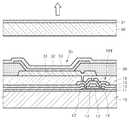
<도면의 주요부분에 대한 부호의 간단한 설명><Brief description of symbols for the main parts of the drawings>
10: 기판 11: 버퍼층10: substrate 11: buffer layer
12: 활성층 13: 게이트 절연막12: active layer 13: gate insulating film
14: 게이트 전극 15: 층간 절연막14
16: 소스 전극17: 드레인 전극16: source electrode 17: drain electrode
18: 패시베이션막30: 유기 발광 소자18: passivation film 30: organic light emitting element
31: 제1 전극32: 유기 발광층31: first electrode 32: organic light emitting layer
33: 제2 전극36: 화소 정의막33: second electrode 36: pixel defining layer
50: 밀봉 부재51: 반사 방지층50: sealing member 51: antireflection layer
본 발명은 유기 발광 표시 장치에 관한 것으로 더 상세하게는 콘트라스트를 향상하는 유기 발광 표시 장치에 관한 것이다. The present invention relates to an organic light emitting display, and more particularly, to an organic light emitting display that improves contrast.
근래에 디스플레이 장치는 휴대가 가능한 박형의 평판 표시 장치로 대체되는 추세이다. 평판 디스플레이 장치 중에서도 유기 또는 무기 발광 표시장치는 자발광형 디스플레이 장치로서 시야각이 넓고 콘트라스트가 우수할 뿐 만 아니라 응답속도가 빠르다는 장점을 가지고 있어서 차세대 디스플레이 장치로 주목 받고 있다. 또한 발광층의 형성 물질이 유기물로 구성되는 유기 발광 표시 장치는 무기 발광 표시 장치에 비해 휘도, 구동 전압 및 응답속도 특성이 우수하고 다색화가 가능하다는 장점을 가지고 있다.Recently, display devices have been replaced by portable thin flat display devices. Among the flat panel display devices, organic or inorganic light emitting display devices are attracting attention as next-generation display devices because they have self-emissive display devices that have a wide viewing angle, excellent contrast, and fast response speed. In addition, an organic light emitting display device in which a light emitting layer is formed of an organic material has advantages in that luminance, driving voltage, and response speed are excellent and multicoloring is possible, compared to an inorganic light emitting display device.
한편 평판 표시 장치는 휴대가 가능하고 야외에서 사용가능 하도록 경량이면서 박형으로 제조한다. 이때 야외에서 화상을 볼 때 햇빛이 반사돼 콘트라스트 및 시인성이 저하되는 문제가 있다. 특히 유기 발광 표시 장치에서는 금속 반사막에서 이러한 반사가 심하여 더 큰 문제가 된다.Meanwhile, the flat panel display device is manufactured to be lightweight and thin so as to be portable and to be used outdoors. In this case, when the image is viewed outdoors, sunlight is reflected, thereby deteriorating contrast and visibility. In particular, in the organic light emitting diode display, the reflection is severe in the metal reflective film, which is a more serious problem.
본 발명은 외광의 반사를 방지하여 콘트라스트가 향상된 유기 발광 표시 장치를 제공할 수 있다.The present invention can provide an organic light emitting display device having improved contrast by preventing reflection of external light.
본 발명은 기판, 상기 기판 상에 형성되고 제1 전극, 투과형 제2 전극 및 상기 제1 전극과 상기 제2 전극 사이에 유기 발광층을 구비하는 유기 발광 소자 및 상기 제1 전극 상에 배치되고 상기 제1 전극이 노출되도록 개구부를 구비하며 흑색 으로 형성되는 화소 정의막을 포함하고, 상기 유기 발광층 및 상기 제2 전극은 상기 개구부로 노출된 제1 전극 상에 차례대로 형성되며, 상기 제2 전극은 인듐옥사이드에 금속 또는 금속산화물이 도핑된 유기 발광 표시 장치를 개시한다.The present invention provides a substrate, an organic light-emitting device formed on the substrate, the organic light emitting device having a first electrode, a second transparent electrode, and an organic light emitting layer between the first electrode and the second electrode, and disposed on the first electrode. And a pixel defining layer having an opening to expose the first electrode and formed in black, wherein the organic emission layer and the second electrode are sequentially formed on the first electrode exposed through the opening, and the second electrode is indium oxide. An organic light emitting diode display doped with a metal or a metal oxide is disclosed.
본 발명에 있어서 상기 화소 정의막은 절연막에 흑색 안료를 혼합하여 형성될 수 있다.In the present invention, the pixel defining layer may be formed by mixing a black pigment on the insulating layer.
본 발명에 있어서 상기 절연막은 폴리 이미드, 아크릴, 아크릴레이트 및 실리카로 이루어지는 군으로부터 선택된 어느 하나를 포함할 수 있다.In the present invention, the insulating film may include any one selected from the group consisting of polyimide, acrylic, acrylate and silica.
본 발명에 있어서 상기 흑색 안료는 카본 블랙 또는 티탄 블랙을 포함할 수 있다.In the present invention, the black pigment may include carbon black or titanium black.
본 발명에 있어서 상기 금속 또는 상기 금속산화물의 일함수의 절대값은 인듐옥사이드의 일함수의 절대값보다 작을 수 있다.In the present invention, the absolute value of the work function of the metal or the metal oxide may be smaller than the absolute value of the work function of the indium oxide.
본 발명에 있어서 상기 금속은 이테르븀(Yb), 칼슘(Ca), 마그네슘(Mg), 사마륨(Sm), 세슘(Cs), 바륨(Ba), 스트론튬(Sr), 이트륨(Y) 및 란탄(La)으로 이루어진 그룹으로부터 선택된 어느 하나를 포함할 수 있다.In the present invention, the metal is ytterbium (Yb), calcium (Ca), magnesium (Mg), samarium (Sm), cesium (Cs), barium (Ba), strontium (Sr), yttrium (Y) and lanthanum (La). It may include any one selected from the group consisting of
본 발명에 있어서 상기 금속산화물은 스트론튬옥사이드, 칼슘옥사이드, 세슘옥사이드, 바륨옥사이드, 이트륨옥사이드 및 란탄옥사이드로 이루어진 그룹으로부터 선택된 어느 하나를 포함할 수 있다.In the present invention, the metal oxide may include any one selected from the group consisting of strontium oxide, calcium oxide, cesium oxide, barium oxide, yttrium oxide and lanthanum oxide.
본 발명에 있어서 상기 밀봉 부재의 양면 중 외부를 향하는 일면의 상부에 형성되는 반사 방지층을 더 포함할 수 있다.In the present invention, it may further include an anti-reflection layer formed on the upper side of one surface of the both sides of the sealing member facing outward.
본 발명에 있어서 상기 반사 방지층은 SiO2, MgF, Al2O3 TiO2, ZrO2, ZnS, ITO, CeF3, Ta2O5 및 Nb2O5 로 이루어진 군으로부터 선택된 어느 하나를 포함할 수 있다.In the present invention, the anti-reflection layer may include any one selected from the group consisting of SiO 2, MgF, Al 2 O 3 TiO 2, ZrO 2, ZnS, ITO, CeF 3, Ta 2 O 5, and Nb 2 O 5.
본 발명에 있어서 상기 제1 전극은 애노오드 전극, 상기 제2 전극은 캐소오드 전극일 수 있다.In the present invention, the first electrode may be an anode electrode, and the second electrode may be a cathode electrode.
이하 첨부된 도면들에 도시된 본 발명에 관한 실시예를 참조하여 본 발명의 구성 및 작용을 상세히 설명한다. Hereinafter, with reference to the embodiments of the present invention shown in the accompanying drawings will be described in detail the configuration and operation of the present invention.
도 1은 본 발명의 일 실시예에 관한 유기 발광 표시 장치를 도시한 개략적인 단면도이다. 유기 발광 표시 장치는 능동 구동형(active matrix type: AM)과 수동 구동형(passive matrix: PM)으로 크게 구별된다. 도 1은 본 발명의 일 실시예에 관한 유기 발광 표시 장치로 능동 구동형(active matrix type: AM)을 도시하고 있으나 본 발명은 이에 한정되지 않고 수동 구동형(passive matrix type: PM)에도 적용할 수 있다.1 is a schematic cross-sectional view of an organic light emitting diode display according to an exemplary embodiment of the present invention. The organic light emitting diode display is largely classified into an active matrix type (AM) and a passive matrix type (PM). 1 illustrates an active matrix type (AM) as an organic light emitting diode display according to an exemplary embodiment of the present invention, but the present invention is not limited thereto and may be applied to a passive matrix type (PM). Can be.
PM형은 양극과 음극이 컬럼(column)과 로우(row)로 배열되어 음극에는 로우 구동 회로로부터 스캐닝 신호가 공급되고 이때, 복수의 로우중 하나의 로우만이 선택된다. 또한 컬럼 구동회로에는 각 화소로 데이터 신호가 입력된다. 한편, AM형은 박막 트랜지스터(thin film transistor:TFT)를 이용해 각 화소 당 입력되는 신호를 제어하는 것으로 방대한 양의 신호를 처리하기에 적합하여 동영상을 구현하기 위한 디스플레이 장치로 각광 받고 있다.In the PM type, the anode and the cathode are arranged in columns and rows so that the cathode is supplied with a scanning signal from a row driving circuit, and only one row of the plurality of rows is selected. In addition, a data signal is input to each pixel in the column driving circuit. On the other hand, the AM type controls a signal input for each pixel by using a thin film transistor (TFT), which is suitable for processing a large amount of signals, and has been in the spotlight as a display device for implementing a video.
도 1에서 볼 수 있는 바와 같이, 본 발명의 일 실시예에 관한 유기 발광 표시 장치는 기판(10), 유기 발광 소자(30) 및 화소 정의막(36)을 포함한다.As shown in FIG. 1, an organic light emitting diode display according to an exemplary embodiment includes a
기판(10)은 SiO2를 주성분으로 하는 투명한 유리 재질로 이루어질 수 있다. 기판(10)은 반드시 이에 한정되는 것은 아니며 투명한 플라스틱 재로 형성할 수도 있다. 플라스틱 기판은 절연성 유기물로 형성할 수 있는데 폴리에테르술폰(PES, polyethersulphone), 폴리아크릴레이트(PAR, polyacrylate), 폴리에테르 이미드(PEI, polyetherimide), 폴리에틸렌 나프탈레이트(PEN, polyethyelenen napthalate), 폴리에틸렌 테레프탈레이드(PET, polyethyeleneterepthalate), 폴리페닐렌 설파이드(polyphenylene sulfide: PPS), 폴리아릴레이트(polyallylate), 폴리이미드(polyimide), 폴리카보네이트(PC), 셀룰로오스 트리 아세테이트(TAC), 셀룰로오스 아세테이트 프로피오네이트(cellulose acetate propinonate: CAP)로 이루어진 그룹으로부터 선택되는 유기물로 이루어질 수 있다.The
화상이 기판(10)방향으로 구현되는 배면 발광형인 경우에 기판(10)은 투명한 재질로 형성해야 한다. 그러나 도 1에 도시된 것과 같이 화상이 기판(10)의 반대 방향으로 구현되는 전면 발광형인 경우에 기판(10)은 반드시 투명한 재질로 형성할 필요는 없다. 이 경우 금속으로 기판(10)을 형성할 수 있다. 금속 기판(10)은 탄소, 철, 크롬, 망간, 니켈, 티타늄, 몰리브덴, 스테인레스 스틸(SUS), Invar 합금, ZInconel 합금 및 Kovar 합금으로 이루어진 군으로부터 선택된 하나 이상을 포함할 수 있으나, 이에 한정되는 것은 아니다. 금속 기판(10)은 금속 포일일 수 있다.When the image is a bottom emission type implemented in the direction of the
기판(10)을 금속 포일이나 플라스틱 등 유연한 소재로 형성하면 유기 발광 표시 장치를 휴대하기도 용이하고 곡면의 벽에도 용이하게 설치할 수 있는 장점이 있다.If the
기판(10)의 상면에는 기판(10)의 평활성과 불순 원소의 침투를 차단하기 위하여 버퍼층(11)을 형성할 수 있다. 버퍼층(11)은 SiO2 및/또는 SiNx 등으로 형성할 수 있다.The
기판(10)의 상면에 박막 트랜지스터(TFT)가 형성되어 있다. 이 박막 트랜지스터(TFT)는 각 화소별로 적어도 하나씩 형성되는 데, 유기 발광 소자(30)에 전기적으로 연결된다.The thin film transistor TFT is formed on the upper surface of the
구체적으로 버퍼층(11)상에 소정 패턴의 활성층(12)이 형성된다. 활성층(12)은 아모퍼스 실리콘 또는 폴리 실리콘과 같은 무기 반도체나 유기 반도체로 형성될 수 있고 소스 영역, 드레인 영역 및 채널 영역을 포함한다.Specifically, the
활성층(12)의 상부에는 게이트 절연막(13)이 형성된다. 게이트 절연막(13)은 금속 산화물 또는 금속 질화물과 같은 무기물로 이루어지거나 절연성 고분자와 같은 유기물로 형성될 수 있다.The
게이트 절연막(13)상부의 소정 영역에는 게이트 전극(14)이 형성된다. 게이트 전극(14)은 TFT 온/오프 신호를 인가하는 게이트 라인(미도시)과 연결되어 있다. 게이트 전극(14)은 Au, Ag, Cu, Ni, Pt, Pd, Al, Mo, 또는 Al:Nd, Mo:W 합금 등과 같은 금속 또는 금속의 합금으로 이루어질 수 있으나, 이에 한정되는 것은 아니다.The
게이트 전극(14)의 상부로는 층간 절연막(15)이 형성되고, 컨택홀을 통해 소 스 전극(16) 및 드레인 전극(17)이 각각 활성층(12)의 소스 및 드레인 영역에 접하도록 형성된다. 소스 전극(16)및 드레인 전극(17)을 이루는 물질은 Au, Pd, Pt, Ni, Rh, Ru, Ir, Os 외에도, Al, Mo, Al:Nd 합금, MoW 합금 등과 같은 2 종 이상의 금속으로 이루어진 합금을 사용할 수 있으며 이에 한정되지는 않는다.An
이렇게 형성된 TFT는 패시베이션막(18)으로 덮여 보호된다. 패시베이션막(18)은 무기 절연막 및/또는 유기 절연막을 사용할 수 있는데 무기 절연막으로는 SiO2, SiNx, SiON, Al2O3, TiO2, Ta2O5, HfO2, ZrO2, BST, PZT 등이 포함될 수 있고, 유기 절연막으로는 일반 범용고분자(PMMA, PS), phenol그룹을 갖는 고분자 유도체, 아크릴계 고분자, 이미드계 고분자, 아릴에테르계 고분자, 아마이드계 고분자, 불소계고분자, p-자일렌계 고분자, 비닐알콜계 고분자 및 이들의 블렌드 등이 포함되도록 할 수 있다. 패시베이션막(18)은 무기 절연막과 유기 절연막의 복합 적층체로도 형성될 수 있다.The TFT thus formed is covered with the
패시베이션막(18) 상부에는 유기 발광 소자의 애노우드 전극이 되는 제1 전극(31)이 형성되고, 이를 덮도록 절연물로 화소 정의막(36)(pixel define layer)이 형성된다. 제1 전극(31)은 반사 전극 또는 투과형 전극일 수 있다. 반사 전극인 경우에 Ag, Mg, Al, Pt, Pd, Au, Ni, Nd, Ir, Cr, Li, Ca 및 이들의 화합물 등으로 형성될 수 있다. 그리고 그 위에 일함수가 높은 ITO, IZO, ZnO, 또는 In2O3 등을 형성하여 이루어질 수 있다.A
화소 정의막(36)은 절연층으로서 흑도가 높은 색상을 갖도록 형성할 수 있 다. 화소 정의막(36)이 백색을 갖는 경우에 전면 발광형 유기 발광 표시 장치는 외광의 반사가 커질 수 있고 결과적으로 콘트라스트가 감소한다. 또한 화소 정의막(36)이 반사형인 경우에도 그러하다.The
본 발명은 화소 정의막(46)이 흑도가 높은 색상을 가지도록 형성되어 유기 발광 표시 장치의 전면으로 입사되는 외광의 반사를 최소화할 수 있다. 외광의 반사를 감소하여 결과적으로 콘트라스트가 향상한다. 화소 정의막(36)은 절연막에 흑색 안료를 혼합하여 형성한다. 화소 정의막(36)을 형성하는 절연막은 폴리 이미드, 아크릴, 아크릴레이트 또는 실리카를 포함한다. 절연막에 혼합할 흑색 안료는 카본 블랙 및 티탄 블랙일 수 있다. 절연막에 혼합할 흑색 안료의 비를 조절하여 화소 정의막(36)의 흑도를 조절할 수 있다.According to the present invention, the pixel defining layer 46 is formed to have a high black color, thereby minimizing reflection of external light incident on the front surface of the OLED display. The reflection of external light is reduced and consequently the contrast is improved. The
화소 정의막(36)에 소정의 개구를 형성한 후, 이 개구로 한정된 영역 내에 유기 발광 소자(30)의 유기 발광층(32)을 형성한다. 그리고, 전체 화소들을 모두 덮도록 유기 발광 소자(30)의 캐소오드 전극이 되는 투과형 제2 전극(33)이 형성된다.After the predetermined opening is formed in the
유기 발광 소자는 전류의 흐름에 따라 빛을 발광하여 화상을 표시하는 것으로 TFT의 드레인 전극(17)에 콘택홀을 통하여 전기적으로 연결된 제1 전극(31), 유기 발광층(32) 및 제2 전극(33)을 포함한다.The organic light emitting diode emits light in accordance with the flow of current to display an image. The organic light emitting diode is a
제1 전극(31)은 포토 리소그래피법에 의해 소정의 패턴으로 형성할 수 있다. 제1 전극(31)의 패턴은 수동 구동형(passive matrix type: PM)의 경우에는 서로 소정 간격 떨어진 스트라이프 상의 라인들로 형성될 수 있고, 능동 구동형(active matrix type: AM)의 경우에는 화소에 대응하는 형태로 형성될 수 있다. 제1 전극(31)의 상부로 제2 전극(33)이 배치되는데 외부단자(미도시)에 연결하여 캐소오드(cathode)전극으로 작용할 수 있다. 제2 전극(33)은 수동 구동형의 경우에는 제1 전극(31)의 패턴에 직교하는 스트라이프 형상일 수 있고 능동 구동형의 경우에는 화상이 구현되는 액티브 영역 전체에 걸쳐 형성될 수 있다.The
도 1에 도시한 것과 같이 제2 전극(33)의 방향으로 화상을 구현하는 전면 발광형(top emission type)일 경우, 제2 전극(33)은 투과형 전극으로 구비될 수 있다. 화소 정의막(36)상에 제2 전극(33)이 형성되므로 입사되는 외광은 화소 정의막(36)보다 제2 전극(33)에 먼저 도달한다. 제2 전극(33)이 금속으로 형성되는 경우에는 외광이 화소 정의막(36)에 도달하기 전에 제2 전극(33)에 도달하여 반사되는 반사되는 외광의 양이 많아진다. 결과적으로 흑색으로 형성되는 화소 정의막(36)의 반사 방지 효과가 미약할 수 있다. 그러므로 제2 전극(33)은 투과형 전극으로 형성한다. 외광이 투과형 제2 전극(33)을 통과한 후에 화소 정의막(36)에 도달할 때 흑색으로 형성되는 화소 정의막(36)으로 인해 외광의 반사가 감소한다.As shown in FIG. 1, when the top emission type implements an image in the direction of the
제2 전극(33)이 투과형 전극이기 위하여 제2 전극(33)은 인듐옥사이드로 형성한다. 그러나 인듐옥사이드만으로 제2 전극(33)을 형성할 경우에 일함수가 높아 발광 효율이 감소할 수 있다. 일함수를 낮추기 위하여 투과형 제2 전극(33)은 인듐옥사이드에 금속 또는 금속산화물을 도핑하여 형성한다. 이 때 금속 또는 금속산화물의 일함수의 절대값은 인듐옥사이드의 일함수의 절대값보다 작다.In order for the
사용할 수 있는 금속은 이테르븀(Yb), 칼슘(Ca), 마그네슘(Mg), 사마륨(Sm), 세슘(Cs), 바륨(Ba), 스트론튬(Sr), 이트륨(Y) 및 란탄(La)으로 이루어진 그룹으로부터 선택된 하나 이상인 것으로 할 수 있다.Metals that can be used are ytterbium (Yb), calcium (Ca), magnesium (Mg), samarium (Sm), cesium (Cs), barium (Ba), strontium (Sr), yttrium (Y), and lanthanum (La). It may be one or more selected from the group consisting of.
또한 사용될 수 있는 금속산화물은 스트론튬옥사이드, 칼슘옥사이드, 세슘옥사이드, 바륨옥사이드, 이트륨옥사이드 및 란탄옥사이드로 이루어진 그룹으로부터 선택된 하나 이상인 것으로 할 수 있다.In addition, the metal oxide that can be used may be at least one selected from the group consisting of strontium oxide, calcium oxide, cesium oxide, barium oxide, yttrium oxide and lanthanum oxide.
제2 전극(33)은 열증착을 이용하여 형성할 수 있다. 열증착 시에 증착 온도가 지나치게 높으면 유기 발광 소자(30)가 손상될 수 있다. 그러므로 본 발명의 제2 전극(33)은 증착을 수행하는 챔버 내에 플라즈마를 형성시킨 상태에서 금속 또는 금속산화물과 인듐옥사이드를 열증착하여 형성할 수 있다. 챔버내에서 플라즈마를 형성시킨 상태에서 제2 전극(33)을 형성하면 증착 공정을 진행하는 온도를 낮출 수 있다.The
제2 전극(33)을 형성하는 방법은 다양하게 변형될 수 있다. 예컨대 금속과 인듐을 소스로 하여 산소 분위기에서 열증착할 수도 있다. 이 경우 열증착과정에서 산소 분위기로 인하여 인듐이 인듐옥사이드가 되고 금속이 금속산화물이 되어 결과적으로 인듐옥사이드에 금속산화물이 도핑된 투과형 제2 전극(33)이 형성될 수 있다. 또는 금속과 인듐옥사이드를 소스로 하여 아르곤 분위기에서 열증착할 수도 있다. 이 경우 아르곤은 불활성기체이므로 증착되는 물질의 조성에 영향을 주지 않는 바, 인듐옥사이드에 금속이 도핑된 투과형 제2 전극(33)이 형성될 수 있다. 물론 금속산화물과 인듐옥사이드를 소스로 하여 아르곤 분위기에서 열증착함으로써 인듐옥사이드에 금속산화물이 도핑된 투과형 제2 전극(33)이 형성될 수도 있다. 또한, 금속산화물과 인듐을 소스로 하여 산소 분위기에서 열증착함으로써, 증착과정에서 인듐이 산화되어 인듐옥사이드에 금속산화물이 도핑된 투과형 제2 전극(33)이 형성될 수도 있다. 그리고 금속산화물과 인듐옥사이드를 소스로 하여 산소 분위기에서 열증착하여 인듐옥사이드에 금속산화물이 도핑된 투과형 제2 전극(33)이 형성될 수도 있다. 물론 금속과 인듐을 소스로 하여 산소와 아르곤이 혼합된 분위기에서 열증착하거나, 금속과 인듐옥사이드를 소스로 하여 산소와 아르곤이 혼합된 분위기에서 열증착함으로써 투과형 제2 전극(33)을 형성할 수도 있다.The method of forming the
한편 제2 전극(33)은 인듐옥사이드에 금속 및 금속산화물이 도핑되도록 형성할 수도 있다. 예컨대 금속 및 금속산화물과 인듐옥사이드를 소스로 하여 아르곤 분위기에서 열증착함으로써, 인듐옥사이드에 금속 및 금속산화물이 도핑된 투과형 제2 전극(33)을 형성할 수 있다. 물론 금속과 인듐을 소스로 하여 산소 분위기에서 열증착함으로써, 인듐이 산화되어 인듐옥사이드가 되어 증착되고, 금속의 일부는 산화되어 금속산화물이 되어 증착되며, 금속의 일부는 산화되지 않고 금속으로 증착되어, 결과적으로 인듐옥사이드에 금속 및 금속산화물이 도핑된 투과형 제2 전극을 형성할 수도 있다. 금속과 인듐이 아니라 금속과 인듐옥사이드를 소스로 하여 산소 분위기에서 열증착함으로써, 금속의 일부는 산화되어 금속산화물이 되어 증착되고 금속의 일부는 산화되지 않고 금속으로 증착되어, 인듐옥사이드에 금속 및 금속산화물이 도핑된 투과형 제2 전극(33)을 형성할 수도 있다. 또한 증착 분위기를 산소로 한정하지 않고 금속과 인듐을 소스로 하여 산소와 아르곤이 혼합된 분위기에서 열증착하거나, 금속과 인듐옥사이드를 소스로 하여 산소와 아르곤이 혼합된 분위기에서 열증착하거나, 금속 및 금속산화물과 인듐옥사이드를 소스로 하여 산소와 아르곤이 혼합된 분위기에서 열증착함으로써 인듐옥사이드에 금속 및 금속산화물이 도핑된 투과형 제2 전극(33)을 형성할 수도 있다.Meanwhile, the
화소 정의막(36)상에 배치되는 제2 전극(43)이 투명하므로 외광이 입사되면 투명한 제2 전극(43)을 투과한 후 흑색의 화소 정의막(36)에 입사된 후 흡수되므로 외광의 반사가 방지된다. 결과적으로 콘트라스트가 증대된다.Since the second electrode 43 disposed on the
제1 전극(31)과 제2 전극(33)의 사이에 개재된 유기 발광층(32)은 제1 전극(31)과 제2 전극(33)의 전기적 구동에 의해 발광한다. 유기 발광층(32)은 저분자 또는 고분자 유기물을 사용할 수 있다. 유기 발광층(32)이 저분자 유기물로 형성되는 경우 유기 발광층(32)을 중심으로 제1 전극(31)의 방향으로 홀 수송층 및 홀 주입층 등이 적층되고, 제2 전극(33) 방향으로 전자 수송층 및 전자 주입층 등이 적층된다. 이외에도 필요에 따라 다양한 층들이 적층될 수 있다. 사용 가능한 유기 재료도 구리 프탈로시아닌(CuPc: copper phthalocyanine), N,N-디(나프탈렌-1-일)-N,N'-디페닐-벤지딘 (N,N'-Di(naphthalene-1-yl)-N,N'-diphenyl-benzidine: NPB) , 트리스-8-하이드록시퀴놀린 알루미늄(tris-8-hydroxyquinoline aluminum)(Alq3) 등을 비롯해 다양하게 적용 가능하다.The organic
한편, 고분자 유기물로 형성된 고분자 유기층의 경우에는 유기 발광층(32)을 중심으로 제1 전극(31)의 방향으로 홀 수송층(Hole Transport Layer: HTL)만이 포함될 수 있다. 상기 고분자 홀 수송층은 폴리에틸렌 디히드록시티오펜 (PEDOT: poly-(2,4)-ethylene-dihydroxy thiophene)이나, 폴리아닐린(PANI: polyaniline) 등을 사용하여 잉크젯 프린팅이나 스핀 코팅의 방법에 의해 제1 전극(31) 상부에 형성되며, 고분자 유기 발광층(32)은 PPV, Soluble PPV's, Cyano-PPV, 폴리플루오렌(Polyfluorene) 등을 사용할 수 있으며 잉크젯 프린팅이나 스핀 코팅 또는 레이저를 이용한 열전사방식 등의 통상의 방법으로 컬러 패턴을 형성할 수 있다.Meanwhile, in the case of the polymer organic layer formed of the polymer organic material, only the hole transport layer (HTL) may be included in the direction of the
유기 발광 소자(30) 상에 유기 발광 소자(30)를 봉지하는 밀봉 부재(50)가 형성된다. 밀봉 부재(50)는 외부의 수분이나 산소 등으로부터 유기 발광 소자(30)를 보호하기 위해 형성한다. 도 1에 도시한 것과 같은 전면 발광형 구조에서는 밀봉 부재(50)는 투명한 재질로 이루어진다. 이를 위해 글라스 기판, 플라스틱 기판 또는 유기물과 무기물의 복수의 중첩된 구조일 수도 있다.The sealing
본 발명의 일 실시예에 의한 유기 발광 표시 장치는 흑색의 화소 정의막(36)을 포함하여 외광의 반사를 감소한다. 또한 화소 정의막(36)상에 형성되는 제2 전극(33)은 투과형이므로 외광의 반사를 감소하는 효과가 줄어들지 않는다.The organic light emitting diode display according to the exemplary embodiment includes a black
도 2 는 본 발명의 다른 실시예에 관한 유기 발광 표시를 도시한 개략적인 단면도이다. 이하에서는 본 발명의 일 실시예와 상이한 점을 중심으로 설명한다. 동일한 참조 부호는 동일한 부재를 나타낸다.2 is a schematic cross-sectional view illustrating an organic light emitting display according to another embodiment of the present invention. Hereinafter will be described focusing on the points different from the embodiment of the present invention. Like reference numerals denote like elements.
도 2를 참조하면 유기 발광 표시 장치는 기판(10), 유기 발광 소자(30), 화소 정의막(36), 밀봉 부재(50) 및 반사 방지층(51)을 포함한다. 반사 방지층(51)은 밀봉 부재(50)의 양면 중 외부를 향하는 일면의 상부에 형성된다. 반사 방지층(51)은 SiO2, MgF, Al2O3 TiO2, ZrO2, ZnS, ITO, CeF3, Ta2O5 및 Nb2O5 로 이루어진 군으로부터 선택된 어느 하나를 포함할 수 있도록 형성할 수 있다. 반사 방지층(51) 은 외부에서 입사되는 외광을 표면에서 산란시키는 방법등을 이용하여 외광의 반사를 억제한다. 또한 반사 방지층(51)은 그 내부에 하드코팅물질을 첨가하여 유기 발광 표시 장치가 외력에 의한 스크래치 등 손상이 생기는 것을 방지할 수 있다.Referring to FIG. 2, the organic light emitting diode display includes a
반사 방지층(51)으로 인해 밀봉 부재(50)상에서 외광의 반사를 방지할 수 있고 그 결과 콘트라스트 향상 효과를 증대할 수 있다.Due to the
본 발명에 관한 유기 발광 표시 장치는 입사되는 외광의 반사를 방지하여 콘트라스트를 향상할 수 있다.The organic light emitting diode display according to the present invention may improve contrast by preventing reflection of incident external light.
도면에 도시된 실시예를 참고로 설명되었으나 이는 예시적인 것에 불과하며, 본 기술 분야의 통상의 지식을 가진 자라면 이로부터 다양한 변형 및 균등한 다른 실시예가 가능하다는 점을 이해할 것이다. 따라서, 본 발명의 진정한 기술적 보호 범위는 첨부된 특허청구범위의 기술적 사상에 의하여 정해져야 할 것이다.Although described with reference to the embodiment shown in the drawings it is merely exemplary, those skilled in the art will understand that various modifications and equivalent other embodiments are possible from this. Therefore, the true technical protection scope of the present invention will be defined by the technical spirit of the appended claims.
Claims (10)
Translated fromKoreanPriority Applications (2)
| Application Number | Priority Date | Filing Date | Title |
|---|---|---|---|
| KR1020070052925AKR100858823B1 (en) | 2007-05-30 | 2007-05-30 | Organic light emitting display |
| US12/038,725US8110981B2 (en) | 2007-05-30 | 2008-02-27 | Organic light-emitting display apparatus |
Applications Claiming Priority (1)
| Application Number | Priority Date | Filing Date | Title |
|---|---|---|---|
| KR1020070052925AKR100858823B1 (en) | 2007-05-30 | 2007-05-30 | Organic light emitting display |
Publications (1)
| Publication Number | Publication Date |
|---|---|
| KR100858823B1true KR100858823B1 (en) | 2008-09-17 |
Family
ID=40023203
Family Applications (1)
| Application Number | Title | Priority Date | Filing Date |
|---|---|---|---|
| KR1020070052925AActiveKR100858823B1 (en) | 2007-05-30 | 2007-05-30 | Organic light emitting display |
Country Status (2)
| Country | Link |
|---|---|
| US (1) | US8110981B2 (en) |
| KR (1) | KR100858823B1 (en) |
Cited By (6)
| Publication number | Priority date | Publication date | Assignee | Title |
|---|---|---|---|---|
| KR101125569B1 (en) | 2010-02-22 | 2012-03-22 | 삼성모바일디스플레이주식회사 | Organic light emitting diode display and method for manufacturing the same |
| KR20120095197A (en)* | 2011-02-18 | 2012-08-28 | 삼성디스플레이 주식회사 | Organic light emitting display and method of manufacturing the same |
| US8723166B2 (en) | 2010-09-06 | 2014-05-13 | Samsung Display Co., Ltd. | Organic light-emitting display apparatus and method of manufacturing the same |
| US9728591B2 (en) | 2015-02-09 | 2017-08-08 | Samsung Display Co., Ltd. | Organic light emitting diode display having an insulating and a light blocking materials covering an inner circumferential surface of a transmissive hole |
| US9923042B2 (en) | 2014-06-13 | 2018-03-20 | Samsung Display Co., Ltd. | Organic light-emitting diode (OLED) display |
| US10559782B2 (en) | 2014-09-05 | 2020-02-11 | Samsung Display Co., Ltd. | Method of manufacturing organic light emitting display apparatus |
Families Citing this family (3)
| Publication number | Priority date | Publication date | Assignee | Title |
|---|---|---|---|---|
| KR102794829B1 (en)* | 2016-08-18 | 2025-04-11 | 삼성디스플레이 주식회사 | Display device and manufacturing method thereof |
| CN106098742A (en)* | 2016-08-18 | 2016-11-09 | 信利(惠州)智能显示有限公司 | Organic light-emitting display device and manufacture method |
| CN110335963A (en)* | 2019-06-21 | 2019-10-15 | 深圳市华星光电技术有限公司 | An electroluminescent display device |
Citations (3)
| Publication number | Priority date | Publication date | Assignee | Title |
|---|---|---|---|---|
| KR20030003745A (en)* | 2000-05-23 | 2003-01-10 | 인터내셔널 비지네스 머신즈 코포레이션 | Optical device with chip level precision alignment |
| JP2003249370A (en) | 2002-02-20 | 2003-09-05 | Samsung Electronics Co Ltd | Active matrix organic light emitting display and method of manufacturing the same |
| KR20050087284A (en)* | 2004-02-26 | 2005-08-31 | 삼성에스디아이 주식회사 | Electro-luminescent display device |
Family Cites Families (7)
| Publication number | Priority date | Publication date | Assignee | Title |
|---|---|---|---|---|
| TW439387B (en)* | 1998-12-01 | 2001-06-07 | Sanyo Electric Co | Display device |
| TW468283B (en)* | 1999-10-12 | 2001-12-11 | Semiconductor Energy Lab | EL display device and a method of manufacturing the same |
| TW594395B (en)* | 2000-09-29 | 2004-06-21 | Nippon Zeon Co | Photoresist composition for insulating film, insulating film for organic electroluminescent element, and process for producing the same |
| JP2003234186A (en)* | 2001-12-06 | 2003-08-22 | Sony Corp | Display device and method of manufacturing the same |
| TWI298003B (en)* | 2002-10-23 | 2008-06-11 | Toppoly Optoelectronics Corp | Top emission light emitting display with reflection layer |
| KR100551783B1 (en) | 2003-01-20 | 2006-02-13 | 엘지전자 주식회사 | DCF directory and file inspection method for TV's electronic frame board and memory card compatibility |
| KR101223718B1 (en)* | 2005-06-18 | 2013-01-18 | 삼성디스플레이 주식회사 | Method for patterning nano conductive film |
- 2007
- 2007-05-30KRKR1020070052925Apatent/KR100858823B1/enactiveActive
- 2008
- 2008-02-27USUS12/038,725patent/US8110981B2/enactiveActive
Patent Citations (3)
| Publication number | Priority date | Publication date | Assignee | Title |
|---|---|---|---|---|
| KR20030003745A (en)* | 2000-05-23 | 2003-01-10 | 인터내셔널 비지네스 머신즈 코포레이션 | Optical device with chip level precision alignment |
| JP2003249370A (en) | 2002-02-20 | 2003-09-05 | Samsung Electronics Co Ltd | Active matrix organic light emitting display and method of manufacturing the same |
| KR20050087284A (en)* | 2004-02-26 | 2005-08-31 | 삼성에스디아이 주식회사 | Electro-luminescent display device |
Cited By (7)
| Publication number | Priority date | Publication date | Assignee | Title |
|---|---|---|---|---|
| KR101125569B1 (en) | 2010-02-22 | 2012-03-22 | 삼성모바일디스플레이주식회사 | Organic light emitting diode display and method for manufacturing the same |
| US8723166B2 (en) | 2010-09-06 | 2014-05-13 | Samsung Display Co., Ltd. | Organic light-emitting display apparatus and method of manufacturing the same |
| KR20120095197A (en)* | 2011-02-18 | 2012-08-28 | 삼성디스플레이 주식회사 | Organic light emitting display and method of manufacturing the same |
| KR101972463B1 (en)* | 2011-02-18 | 2019-08-19 | 삼성디스플레이 주식회사 | Organic light emitting display and method of manufacturing the same |
| US9923042B2 (en) | 2014-06-13 | 2018-03-20 | Samsung Display Co., Ltd. | Organic light-emitting diode (OLED) display |
| US10559782B2 (en) | 2014-09-05 | 2020-02-11 | Samsung Display Co., Ltd. | Method of manufacturing organic light emitting display apparatus |
| US9728591B2 (en) | 2015-02-09 | 2017-08-08 | Samsung Display Co., Ltd. | Organic light emitting diode display having an insulating and a light blocking materials covering an inner circumferential surface of a transmissive hole |
Also Published As
| Publication number | Publication date |
|---|---|
| US20080297032A1 (en) | 2008-12-04 |
| US8110981B2 (en) | 2012-02-07 |
Similar Documents
| Publication | Publication Date | Title |
|---|---|---|
| KR101058113B1 (en) | Thin film transistor and organic light emitting display | |
| KR100858823B1 (en) | Organic light emitting display | |
| US8461591B2 (en) | Organic light emitting display apparatus and method of manufacturing the same | |
| US8106583B2 (en) | Organic light emitting display apparatus | |
| US8941133B2 (en) | Organic light-emitting display apparatus and method of manufacturing the same | |
| EP1930968A2 (en) | Organic light emitting display apparatus | |
| KR100958642B1 (en) | Organic light emitting display and manufacturing method thereof | |
| US20100033078A1 (en) | Organic light emitting display device | |
| KR20100007266A (en) | Organic light emitting display apparatus and method of manufacturing thereof | |
| US7898175B2 (en) | Organic light emitting display apparatus with an enhanced viewing angle | |
| US8227845B2 (en) | Organic light emitting display | |
| KR100932935B1 (en) | Organic light emitting device and organic light emitting display device including the same | |
| KR100846599B1 (en) | OLED display and manufacturing method thereof | |
| US8888547B2 (en) | Organic light-emitting display apparatus and method of manufacturing the same | |
| KR20080014328A (en) | OLED display and manufacturing method thereof | |
| KR101753773B1 (en) | Organic light emitting display apparatus and method of manufacturing thereof | |
| KR100795815B1 (en) | Organic light emitting display | |
| KR100863907B1 (en) | Organic light emitting display | |
| KR100787465B1 (en) | Organic light emitting display | |
| KR100927584B1 (en) | OLED display and manufacturing method thereof | |
| KR20160047450A (en) | Organic light emitting display apparatus and method of manufacturing thereof | |
| KR100964233B1 (en) | Flat panel display |
Legal Events
| Date | Code | Title | Description |
|---|---|---|---|
| A201 | Request for examination | ||
| PA0109 | Patent application | Patent event code:PA01091R01D Comment text:Patent Application Patent event date:20070530 | |
| PA0201 | Request for examination | ||
| E902 | Notification of reason for refusal | ||
| PE0902 | Notice of grounds for rejection | Comment text:Notification of reason for refusal Patent event date:20080428 Patent event code:PE09021S01D | |
| E701 | Decision to grant or registration of patent right | ||
| PE0701 | Decision of registration | Patent event code:PE07011S01D Comment text:Decision to Grant Registration Patent event date:20080828 | |
| GRNT | Written decision to grant | ||
| PR0701 | Registration of establishment | Comment text:Registration of Establishment Patent event date:20080910 Patent event code:PR07011E01D | |
| PR1002 | Payment of registration fee | Payment date:20080911 End annual number:3 Start annual number:1 | |
| PG1601 | Publication of registration | ||
| PR1001 | Payment of annual fee | Payment date:20110829 Start annual number:4 End annual number:4 | |
| FPAY | Annual fee payment | Payment date:20120831 Year of fee payment:5 | |
| PR1001 | Payment of annual fee | Payment date:20120831 Start annual number:5 End annual number:5 | |
| FPAY | Annual fee payment | Payment date:20130830 Year of fee payment:6 | |
| PR1001 | Payment of annual fee | Payment date:20130830 Start annual number:6 End annual number:6 | |
| FPAY | Annual fee payment | Payment date:20140901 Year of fee payment:7 | |
| PR1001 | Payment of annual fee | Payment date:20140901 Start annual number:7 End annual number:7 | |
| FPAY | Annual fee payment | Payment date:20180829 Year of fee payment:11 | |
| PR1001 | Payment of annual fee | Payment date:20180829 Start annual number:11 End annual number:11 | |
| FPAY | Annual fee payment | Payment date:20190822 Year of fee payment:12 | |
| PR1001 | Payment of annual fee | Payment date:20190822 Start annual number:12 End annual number:12 | |
| PR1001 | Payment of annual fee | Payment date:20200901 Start annual number:13 End annual number:13 | |
| PR1001 | Payment of annual fee | Payment date:20210825 Start annual number:14 End annual number:14 | |
| PR1001 | Payment of annual fee | Payment date:20240822 Start annual number:17 End annual number:17 |